

TOKO TK75003DIMG Datasheet
TK75003
75003
PWM CONTROLLER
FEATURES
■ Power Factor Correction/Line Harmonics
Reduction to Meet IEC1000-3-2 Requirements
■ Optimized for Off-Line Operation
■ Maximum Duty Ratio 88% (typ.)
■ Frequency Reduction for Improved Overcurrent
Protection
■ Low Standby Current for Current-Fed Start-Up
■ Current-Mode or Voltage-Mode Control
■ Internal User-Adjustable Slope Compensation
■ Functionally Integrated & Simplified 5-Pin Design
DESCRIPTION
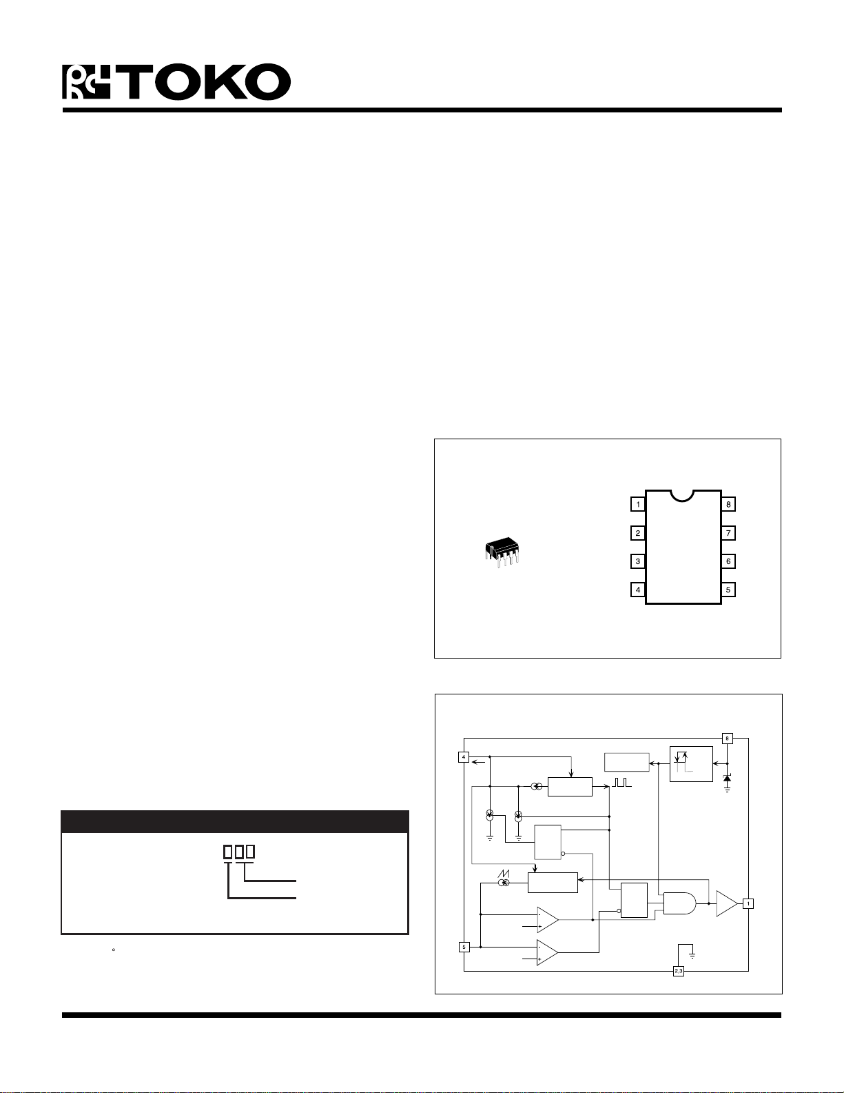
The TK75003 is a simple primary side controller optimized
for off-line switching power supplies including power factor
correctors. It is suitable for both voltage-mode and currentmode control and has advanced features not available in
controllers with a higher pin count. The key to full
functionality in a 5-pin design is that the current signal and
the error signal are added together and fed into the
feedback pin. A sawtooth current flowing out of the feedback
pin provides a slope compensation ramp (in current-mode
applications) or a PWM ramp (in voltage-mode
applications), in proportion to the resistance terminating
that pin. If the sum of the current sense signal, error signal
and ramp signal exceeds the Overcurrent Detector
threshold indicating that the Current Control Detector has
lost control of the switch current, the charging current of
the timing capacitor will be reduced to about 25% for the
remainder of the clock period. The reduced charging
current causes no more than a one-third reduction in
switching frequency, effectively preventing short-circuit
current runaway.
ORDERING INFORMATION
TK75003D
Tape/Reel Code
Temperature Code
TEMP. CODE (OPTIONAL)
I: -40 to +85 C
TAPE/REEL CODE
MG: Magazine
APPLICATIONS
■ Power Factor Correction Converters
■ Off-Line Power Supplies
■ Industrial Power Supplies
■ Telecom Power Supplies
■ Off-Line Battery Chargers
TK75003
DRV
GND NC
GND
T
Note: Pins 2 and 3 must be externally
connected for proper operation.
BLOCK DIAGRAM
I
CT
C
T
FB
I
FR
146 µA
1.35 V
0.98 V
I
CHG
205 µA
I
DS
2 mA
Q
SLOPE
COMPENSATION
OSCILLATOR
R
FREQUENCY
REDUCTION
LATCH
S
OVERCURRENT
DETECTOR
CURRENT
CONTROL
DETECTOR
BANDGAP
REFERENCE
f
CLK
PWM LATCH
S
R
10.5 V
Q
GND
UVLO
14.5 V
V
CC
NC
FBC
V
CC
17.5 V
DRV
January 1999 TOKO, Inc. Page 1

TK75003
ABSOLUTE MAXIMUM RATINGS
Supply Voltage (Low Impedance Source)................ 16 V
Supply Voltage (ICC < 30 mA) ...................... Self Limiting
Power Dissipation (Note 1) ................................ 825 mW
Output Energy (Capacitive Load).............................. 5 µJ
CT and FB Pins ........................................................ 16 V
TK75003 ELECTRICAL CHARACTERISTICS
Test Conditions: VCC = 13 V, CCC = 4.7 µF, CT = 800 pF, C
Typical numbers apply at TA = 25 °C, unless otherwise specified.
LOBMYSRETEMARAPSNOITIDNOCTSETNIMPYTXAMSTINU
Junction Temperature ...........................................150 °C
Storage Temperature Range ................... -55 to +150 °C
Operating Temperature Range ...................-20 to +80 °C
Extended Temperature Range................... -40 to +85 °C
Lead Soldering Temperature (10 s) ......................235 °C
= 1000 pF, TA = Tj = Full Operating Temperature Range.
DRV
I
I
V
V
V
V
)TRATS(CC
)NO(CC
)NO(CC
)FFO(CC
TSYH
)PMALC(CC
siseretsyHOLVU 8.20.4V
C(NOITCESROTALLICSO
f
VRD
V
)KP(TC
V
)LV(TC
I
)SID(TC
C
)XAM(T
egatloVkaeP 5.22.39.3V
egatloVyellaV 1.1V
tnerruCylppuSpu-tratSVotecruoStnerruC
tnerruCylppuSgnitarepO 5.410.91Am
NOegatloVOLVUVCC)3etoN(,drawpUspeewS5.215.410.61V
FFOegatloVOLVUV
egatloVpmalClanretnII
)NIP
T
niPVRDtaycneuqerF
CC
T
AT=j
T
AT=j
CC
C°52=09001011zHk
tnerruCegrahcsiD 0.18.10.3Am
ecnaticapaCgnimiTmumixaM 7.4Fn
niP5.00.1Am
CC
drawnwoDspeewS0.95.010.21V
)3etoN(,Am52=0.615.710.91V
)C°08ot02-(egnaRlluF=08511zHk
)NIPBF(SNOITCESNOITCUDERYCNEUQERFDNAKCABDEEF,ROTCETEDTNERRUC
T
V
DCC
V
DCO
t
DP,CO,BF
t
DP,CC,BF
i
)KP(CS
tnerruC
rotceteDlortnoCtnerruC
egatloVecnerefeR
rotceteDtnerrucrevO
egatloVecnerefeR
kaePnoitasnepmoCepolS
AT=j
T
AT=j
T
AT=j
T
AT=j
niPVRDotyaleDnoitagoporPV
BF
niPVRDotyaleDnoitagoporPVBF)4etoN(,V02.1ot0morfspetS08081sn
V=
V
TC
C°52=059.0089.0010.1V
)C°08ot02-(egnaRlluF=529.0530.1V
C°52=023.1053.1083.1V
)C°08ot02-(egnaRlluF=503.1593.1V
V2ot0morfspetS06031sn
)KP(TC
T,
AT=j
)2etoN(,C°52=542-002-551-Aµ
i
)LV(CS
i
)LV-KP(CS
tnerruC
yellaV
yellaVnoitasnepmoCepolS
otkaePnoitasnepmoCepolS
V=
V
TC
V=
V
TC
)LV(TC
)LV(TC
T,
AT=j
T,
AT=j
)2etoN(,C°52=56-04-51-Aµ
)2etoN(,C°52=002-061-021-Aµ
Page 2 January 1999 TOKO, Inc.
TK75003 ELECTRICAL CHARACTERISTICS (CONT.)
Test Conditions: VCC = 13 V, CCC = 4.7 µF, CT = 800 pF, C
Typical numbers apply at TA = 25 °C, unless otherwise specified.
LOBMYSRETEMARAPSNOITIDNOCTSETNIMPYTXAMSTINU
= 1000 pF, TA = Tj = Full Operating Temperature Range.
DRV
)GNIMITNOITCETORPTNERRUCREVO(RECUDERYCNEUQERF
TK75003
f
f/
)RF(VRD
VRD
oitaR
noitcudeRycneuqerF
V
BF
V6.1,V2.1=020304%
)NIPVRD(NOITCESTUPTUO
D
t
t
V
V
Note 1: Power dissipation is 825 mW when mounted. Derate at 6.6 mW/°C for operation above 25 °C.
Note 2: For temperature dependence refer to "Slope Compensation Peak Current vs. Temperature" graph.
Note 3: The UVLO "on" voltage is guaranteed always to be below the internal clamp voltage.
Note 4: Guaranteed by design; not 100% tested.
)XAM(VRD
)ESIR(VRD
)LLAF(VRD
)HGIH(VRD
)WOL(VRD
emiTesiRV,daolFp0001
emiTllaFV,daolFp0001
oitaRytuDmimixaM588819%
CC
CC
I
HGIHegatloVtuptuO
WOLegatloVtuptuO
VRD
I
VRD
I
VRD
I
VRD
I
VRD
Am04-=1.010.11V
Am001-=0.018.01V
Am04=1.052.0V
Am001=2.005.0V
,Am5=VCCV9=0.105.1V
V51=5257sn
V51=5257sn
January 1999 TOKO, Inc. Page 3

TK75003
TEST CIRCUIT
(mA)
CC
I
0.6
0.4
20
16
12
SUPPLY CURRENT
VS.
SUPPLY VOLTAGE
DEVICE ON
STANDBY
OSCILLOSCOPE
1000 pF
C
800 pF
DRV
GND
GND
T
OSCILLOSCOPE
T
V
CC
NC
NC
FBC
1 µF
20 k
C
CC
4.7 µF
TYPICAL PERFORMANCE CHARACTERISTICS
FREQUENCY AT DRV PIN
TIMING CAPACITANCE
6
10
5
10
TA = 85 °C
4
10
FREQUENCY (Hz)
TA = -40 °C
VS.
CURRENT CONTROL REFERENCE
1.00
0.98
(V)
0.96
CCD
V
0.94
0.92
VS.
TEMPERATURE
0.0
0 4 8 12 16 18
VCC (V)
SLOPE COMPENSATION PEAK
CURRENT
VS.
TEMPERATURE
10
10 100 1000 10000
CT (pF)
INPUT CURRENT
VS.
FREQUENCY AT DRV
60
0.90
-40 0 40 80 120
TEMPERATURE (°C)
FREQUENCY REDUCTION RATIO
TEMPERATURE
50
3
-100
50
-140
(µA)
-180
SC(PK)
i
-220
-260
-40 0 40 80 120
TEMPERATURE (°C)
40
(mA)
CC
I
30
C
DRV
= 1 nF
C
DRV
20
C
10
0 400 800 1200 1600
FREQUENCY (kHz)
= 500 pF
= 0 nF
DRV
48
46
FREQ. REDUCTION RATIO (%)
44
-40 0 40 80 120
TEMPERATURE (°C)
Page 4 January 1999 TOKO, Inc.
VS.

TYPICAL PERFORMANCE CHARACTERISTICS (CONT.)
SLOPE COMPENSATION RAMP
RFB = 3 K to GND
600
CT = 800 pF
450
(mV)
300
FB
V
150
0
0 5 10 15 20
TIME (µs)
i
SC(PK)
i
SC(PK - VL)
i
SC(VL)
TK75003
January 1999 TOKO, Inc. Page 5
 Loading...