

Page 1
20W Hi-Fi AUDIOPOWER AMPLIFIER
DESCRIPTION
The TDA2040 is a monolithicintegrated circuit in
Pentawatt package,intendedforuse asan audio
class ABamplifier.Typicallyit provides22W output
power (d = 0.5%) at V
provides high output current and has very low
harmonic and cross-over distortion. Further the
deviceincorporatesapatentedshortcircuitprotection system comprising an arrangement for automaticallylimitingthedissipatedpowersoastokeep
the working point of the output transistors within
their safe operating area. A thermal shut-down
system is also included.
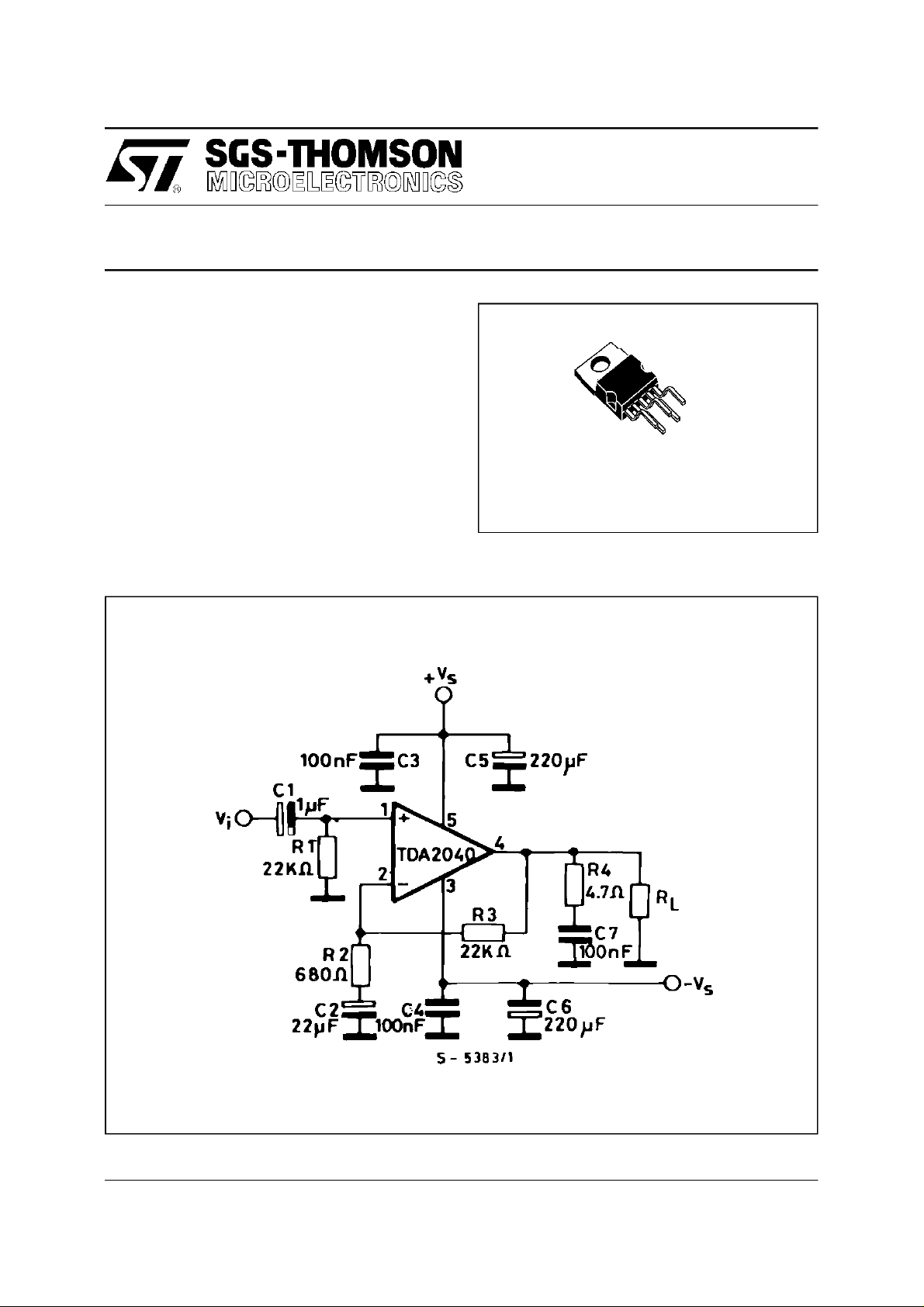
TEST CIRCUIT
= 32V/4Ω . The TDA2040
s
TDA2040
PENTAWATT
ORDERING NUMBER : TDA2040V
December 1995
1/13
Page 2
TDA2040
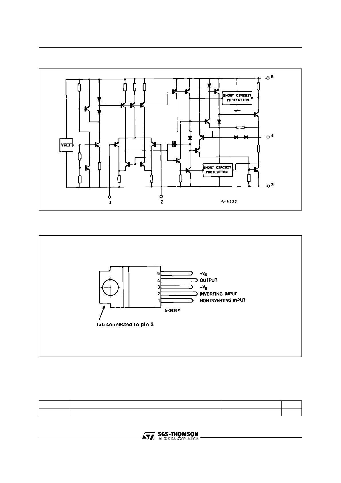
SCHEMATICDIAGRAM
PIN CONNECTION
THERMALDATA
Symbol Parameter Value Unit
R
th j-case
Thermal Resistance Junction-case Max. 3 °C/W
2/13
Page 3
TDA2040
ABSOLUTEMAXIMUM RATINGS
Symbol Parameter Value Unit
V
s
V
V
I
o
P
tot
T
stg,Tj
ELECTRICALCHARACTERISTICS
(refer to the testcircuit, V
Symbol Parameter Test Conditions Min. Typ. Max. Unit
V
s
I
d
I
b
V
os
I
os
P
o
BW Power Bandwidth P
G
v
G
v
d Total Harmonic Distortion P
e
N
i
N
R
i
SVR Supply Voltage Rejection R
η Efficiency f = 1kHz
T
j
Supply Voltage ± 20 V
Input Voltage V
i
DifferentialInput Voltage ± 15 V
i
s
Output Peak Current (internally limited) 4 A
Power Dissipation at T
=75°C25W
case
Storage and Junction Temperature – 40 to + 150 °C
= ± 16V, T
S
=25oC unlessotherwise specified)
amb
Supply Voltage ± 2.5 ± 20 V
Quiescent Drain Current Vs= ± 4.5V
= ± 20V 4530100mAmA
V
s
Input Bias Current Vs= ± 20V 0.3 1 µA
Input Offset Voltage Vs= ± 20V ± 2 ± 20 mV
Input Offset Current ± 200 nA
Output Power d = 0.5%, T
f = 1kHz R
f = 15kHz R
= 1W, RL=4Ω 100 kHz
o
case
=60°C
=4Ω
L
=8Ω
R
L
=4Ω
L
201522
12
18
Open Loop Voltage Gain f = 1kHz 80 dB
Closed Loop Voltage Gain f = 1kHz 29.5 30 30.5 dB
= 0.1to 10W, RL=4Ω
o
f = 40 to 15000Hz
f = 1kHz
Input Noise Voltage B = Curve A
B = 22Hz to 22kHz
Input Noise Current B = Curve A
B = 22Hz to 22kHz
0.08
0.03
2
310
50
80 200
Input Resistance (pin 1) 0.5 5 MΩ
=4Ω,Rg= 22kΩ,Gv= 30dB
L
f = 100Hz, V
P
= 12W RL=8Ω
o
= 22W RL=4Ω
P
o
ripple
= 0.5V
RMS
40 50 dB
66
63
Thermal Shut-down JunctionTemperature 145 °C
W
%
µV
µV
pA
%
3/13
Page 4
TDA2040
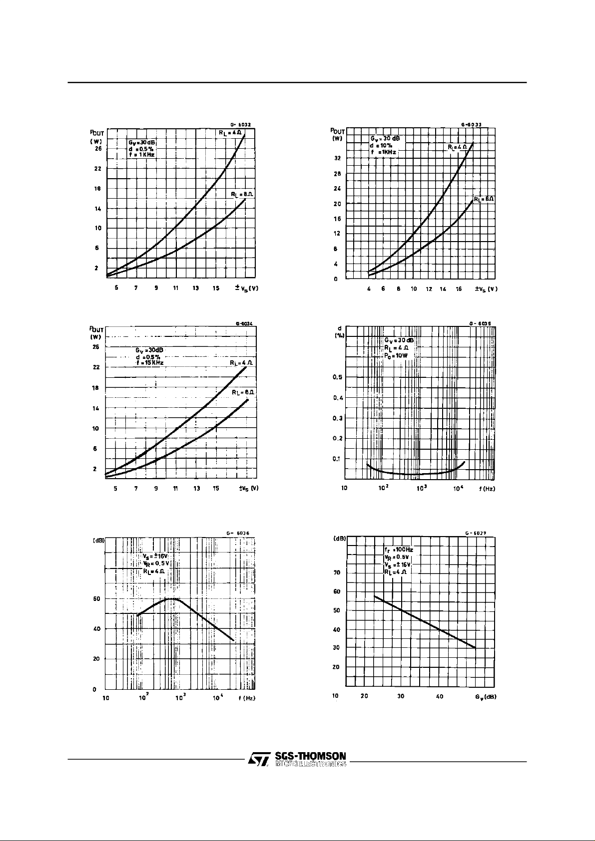
Figure1 : OutputPower versus Supply Voltage Figure 2 : OutputPower versus Supply Voltage
Figure3 : OutputPower versus Supply Voltage Figure 4 : Distortion versus Frequency
Figure5 : Supply Voltage Rejectionversus
Frequency
4/13
Figure6 : SupplyVoltage Rejectionversus
VoltageGain
Page 5

TDA2040
Figure7 : QuiescentDrain Current versus
Supply Voltage
Figure9 : PowerDissipation versusOutput
Power
Figure8 : OpenLoop Gain versus Frequency
5/13
Page 6

TDA2040
Figure10 : Amplifier with Split Power Supply
Figure11: P.C.Boardand Components Layoutfor the Circuit of Figure 10 (1:1 scale)
6/13
Page 7

Figure12 : Amplifier with Split Power Supply (see Note)
Note : In this case of highly inductive loadsprotection diodes may be necessary.
Figure13 : P.C.Board and Components Layout for the Circuit of Figure 12 (1:1 scale)
TDA2040
7/13
Page 8

TDA2040
Figure14 : 30W Bridge Amplifierwith Split Power Supply
Figure15 : P.C.Board and Components Layout for the Circuit of Figure 14 (1:1 scale)
8/13
Page 9

Figure16 : TwoWayHi-Fi System with Active Crossover
TDA2040
Figure 17 : P.C. Boardand ComponentsLayout for the Circuit of Figure 16 (1:1 scale)
9/13
Page 10

TDA2040
Figure18 : FrequencyResponse Figure19 : PowerDistribution versus Frequency
MULTIWAY SPEAKERSYSTEMS AND ACTIVE
BOXES
Multiway loudspeaker systems provide the best
possible acoustic performance since each loudspeaker is specially designed and optimized to
handle a limited range of frequencies.Commonly,
these loudspeakersystems dividetheaudio spectruminto two, three or four bands.
TomaintainaflatfrequencyresponseovertheHi-Fi
audio range the bands covered by each loudspeakermust overlap slightly. Imbalancebetween
the loudspeakers produces unacceptable results
therefore it is important to ensure that each unit
generates the correct amount of acoustic energy
for its segment of the audio spectrum. In this respect it is also important to know the energy distribution of the music spectrum determine the cutoff
frequenciesofthecrossoverfilters (seeFigure19).
As an example, a 100W three-way system with
crossover frequencies of 400Hz and 3kHz would
require50W for the woofer, 35Wfor the midrange
unitand 15W for the tweeter.
Both active and passive filters can be used for
crossoversbut today activefilters costsignificantly
less than a good passivefilter using air-cored inductorsandnon-electrolyticcapacitors.Inaddition,
active filters do not suffer from the typicaldefects
of passive filters :
- powerloss
- increased impedance seen by the loudspeaker
(lowerdamping)
- difficulty of precise design due to variable loudspeakerimpedance
Obviously,active crossovers can only be used if a
poweramplifierisprovidedfor eachdriveunit.This
makes it particularly interesting and economically
soundto use monolithic power amplifiers. In some
applications, complex filters are not really necessary and simple RC low-pass and high-pass networks(6dB/octave) can be recommended.
The results obtained are excellent because this is
the best type of audio filter and the only one free
from phase and transientdistortion.
The rather poor out of band attenuation of single
RC filters means that the loudspeakermust operate linearlywell beyondthe crossoverfrequencyto
avoid distortion.
A more effective solution, named ”Active Power
Filter” by SGS is shownin Figure20.
Figure20 : Active PowerFilter
The proposed circuit can realize combined power
amplifiers and 12dB/octave or 18dB/octave highpass or low-pass filters.
In practice, at the input pins of the amplifier two
equal and in-phase voltages are available, as requiredfor the activefilter operation.
10/13
Page 11

TDA2040
Theimpedanceat thepin (-)isoftheorderof 100Ω,
PRATICALCONSIDERATION
while that of the pin (+) is very high, which is also
what was wanted.
C1 = C2 = C3 R1 R2 R3
22 nF 8.2 kΩ 5.6 kΩ 33 kΩ
The component values calculated for fc= 900Hz
using a Bessel 3rd order Sallenand Key structure
PrintedCircuit Board
The layout shown in Figure11 should be adopted
by the designers. If different layouts are used, the
groundpoints of input 1 and input 2 must be well
decoupledfrom the gorund return of the outputin
whicha high current flows.
are :
In theblock diagram ofFigure21isrepresentedan
activeloudspeakersystemcompletely realizedusing power integrated circuit, rather than the traditional discrete transistors on hybrids, very high
AssemblySuggestion
No electrical isolationis neededbetweenthe pack-
age and the heatsink with single supply voltage
configuration.
quality is obtained by driving the audio spectrum
into three bands using active crossovers
(TDA2320A) and a separate amplifier and loudspeakersfor each band.
A modern subwoofer/midrange/tweetersolution is
used.
ApplicationSuggestions
The recommended values of the components are
those shown on application circuit of Fig. 10. Dif-
ferentvaluescan be used. The followingtable can
help the designer.
Figure21 : High Power Active LoudspeakerSystem usingTDA2030Aand TDA2040
Comp.
C3, C4 0.1µF Supply voltage bypass Danger of oscillation
C5, C6 220µF Supply voltage bypass Danger of oscillation
(*) The value of closed loop gain must be higher than 24dB
Recom.
Value
R1 22kΩ Non inverting input biasing Increase of input impedance Decrease of input impedance
R2 680Ω Closed loop gain setting Decrease of gain (*) Increase of gain
R3 22kΩ Closedloop gain setting Increase of gain Decrease of gain (*)
R4 4.7Ω Frequency stability Danger of oscillation at high
C1 1µF InputDC decoupling Increase of low frequencies cut-off
C2 22µF Inverting DC decoupling Increase of low frequencies cut-off
C7 0.1µF Frequency stability Danger of oscillation
Purpose
frequencies with inductive loads
Larger than
Recommended Value
Smaller than
Recommended Value
11/13
Page 12

TDA2040
PENTAWATT PACKAGE MECHANICAL DATA
DIM.
MIN. TYP. MAX. MIN. TYP. MAX.
mm inch
A 4.8 0.189
C 1.37 0.054
D 2.4 2.8 0.094 0.110
D1 1.2 1.35 0.047 0.053
E 0.35 0.55 0.014 0.022
F 0.8 1.05 0.031 0.041
F1 1 1.4 0.039 0.055
G 3.4 0.126 0.134 0.142
G1 6.8 0.260 0.268 0.276
H2 10.4 0.409
H3 10.05 10.4 0.396 0.409
L 17.85 0.703
L1 15.75 0.620
L2 21.4 0.843
L3 22.5 0.886
L5 2.6 3 0.102 0.118
L6 15.1 15.8 0.594 0.622
L7 6 6.6 0.236 0.260
M 4.5 0.177
M1 4 0.157
Dia 3.65 3.85 0.144 0.152
A
H3
L
L1
C
D1
L5
Dia.
L7
L6
L2
L3
D
F1
H2
E
MM1
G1
G
F
12/13
Page 13

TDA2040
Information furnished is believedto be accurate andreliable. However, SGS-THOMSON Microelectronics assumes no responsibility for the
consequences of use of such information nor for any infringementof patents or other rights of third parties which may result from its use. No
licenseis granted by implication or otherwiseunder any patent or patent rights of SGS-THOMSONMicroelectronics. Specifications mentioned in this publication are subject to change without notice.This publication supersedes and replaces all information previously supplied.
SGS-THOMSON Microelectronics products are not authorized for use as critical components in life support devices or systems without express written approval of SGS-THOMSON Microelectronics.
1996 SGS-THOMSONMicroelectronics All Rights Reserved
Australia - Brazil - Canada - France - Germany - Hong Kong - Italy - Japan - Korea - Malaysia - Malta - Morocco -The Netherlands -
Singapore - Spain - Sweden - Switzerland - Taiwan - Thaliand - United Kingdom - U.S.A.
SGS-THOMSON Microelectronics GROUP OF COMPANIES
13/13
 Loading...