

Page 1
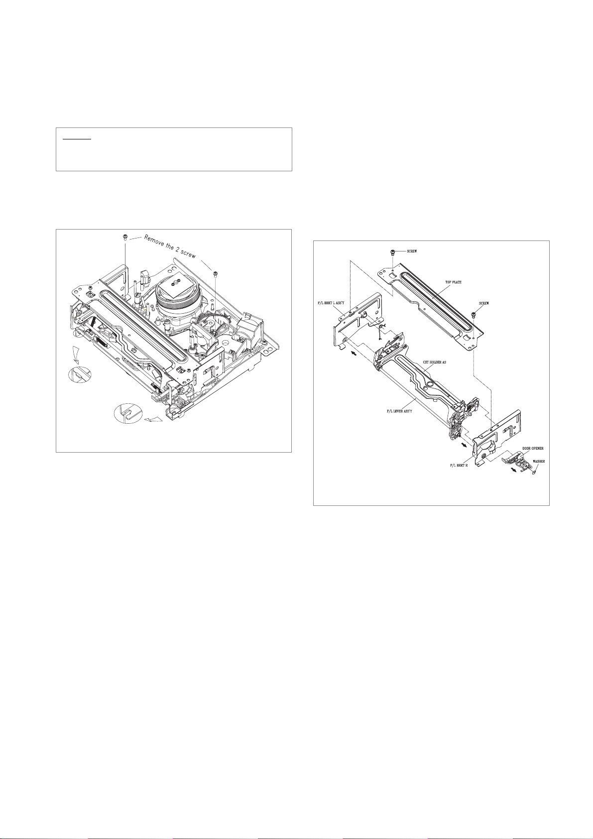
3.1 Removal of the FRONT LOADING Ass’y
(Fig. 3.1)
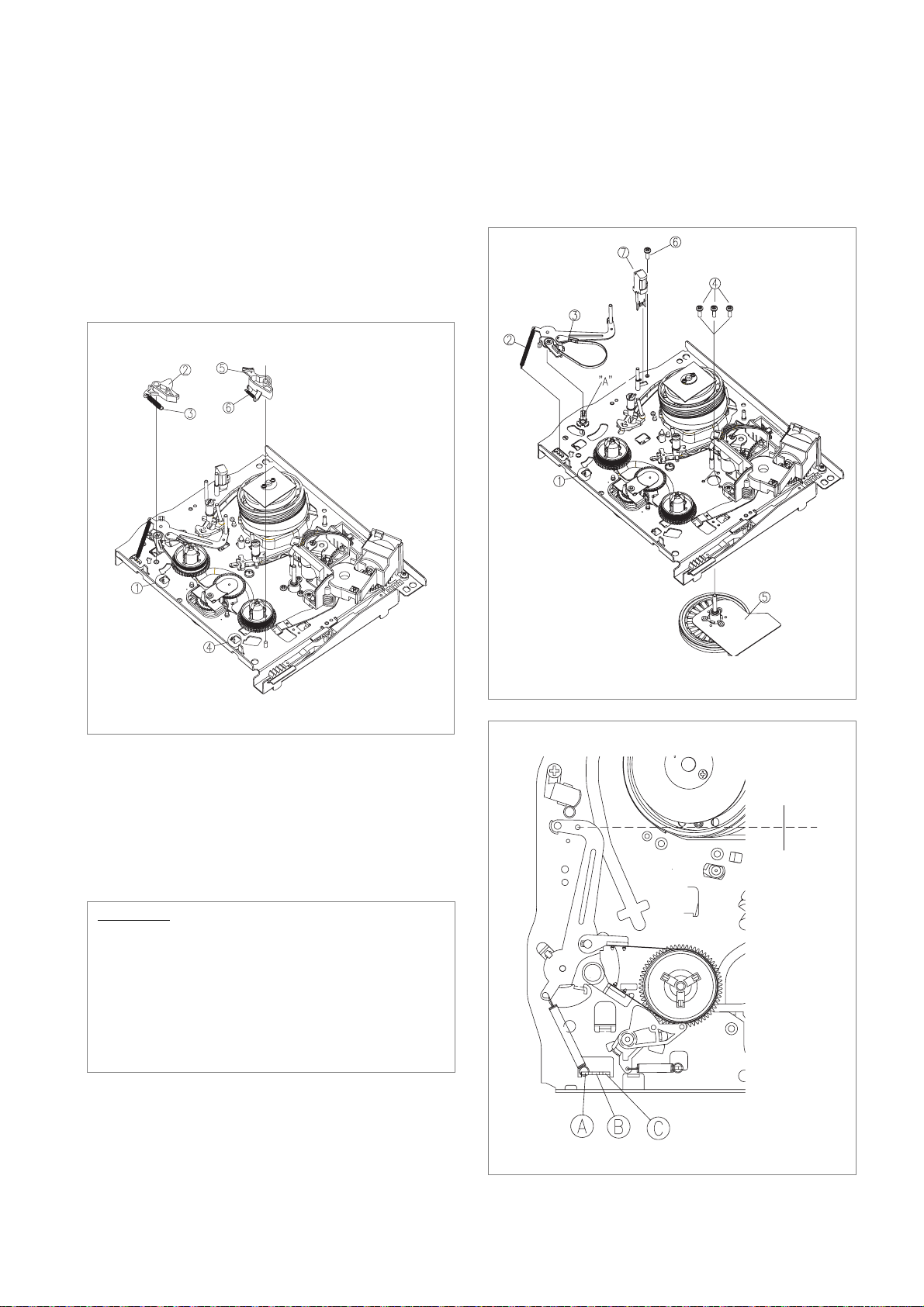
a. Unscrew the 2 screw holding the F/L.
b. Separate the F/L ASS`Y from the MAIN BASE settling
down point by lifting the rear part of F/L(Screw hole).
3.2 Disassembly of FRONT LOADING Ass’y
(FIg. 3.2~3.5)
a. Remove the one WASHER for holding the door opener
and separtate F/L Assembly by moving the DOOR
OPENER in the direction of arrow.
b. Remove the 2 screw holding the TOP PLATE and sepa-
rate the CASSETT HOLDER ASS`Y by moving the
FL BRKT L and FL BRKT R in the direction of arrow
(Fig. 3.2)
3. DISASSEMBLY AND REPLACEMENT
NOTE:
REMOVE THE FRONT LOADING ASS`Y IN EJECT
MODE
Fig. 3.1 Diassembly of the FRONT LOADING ASS`Y
Fig. 3.2 Diassembly of the FRONT LOADING ASS`Y
Page 2
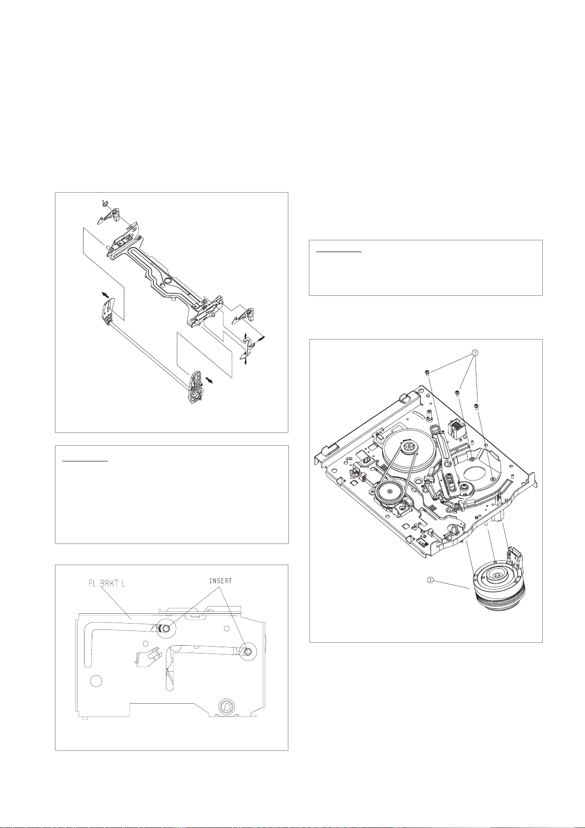
c. Separate the LOADING LEVER ASS`Y by pressing
the connection point from the CASSETTE HOLDER
ASS`Y.(Fig. 3.3)
d. Remove the SAFETY SPRING connecting the SAFETY
LEVER and CASSETTE HOLDER PLATE.(Fig. 3.3)
e. Remove the RELEASE SPRING connecting the
RELEASE LEVER and SAFETY LEVER.(Fig3.3)
3. 3 Disassembly of DRUM Ass’y (Fig. 3.5)
a. Turn over the DECK MECHANISM and holding the
DRUM TOTAL ASS`Y @ with hands , remove the 3
screw holding the drum total assembly with main base.
b. Separatet the DRUM TOTAL ASS`Y from the deck pay-
ing attention there is no damage on the surface of VIDEO
HEAD and DRUM.
c. Assembly step is the reverse way of diassembly.
DISASSEMBLY AND REPLACEMENT (CONTINUED)
CAUTION:
Assemble the FRONT LOADING ASS`Y in the reverse
step of diassembly. Confirm that two bosses on the left
side of the CASSETTE HOLDER ASS`Y are inserted in
the groove on the left side of the top plate. Insert two
bosses on the right side of the CASSETTE HOLDER
ASS`Y into the groove of the F/L BRACKET R.(Fig. 3.4)
FIg. 3.3 Disassembly of the CASSETTE HOLDER Ass’y
FIg. 3.4 Assembly of the FL Ass’y
CAUTION:
• After the assembly of the DRUM TOTAL ASS`Y,
check out if DECK mecahnism operate smoothly and
adjustment of tape transmission section is OK.
FIg. 3.5 Diassembly of DRUM ASS`Y
Page 3
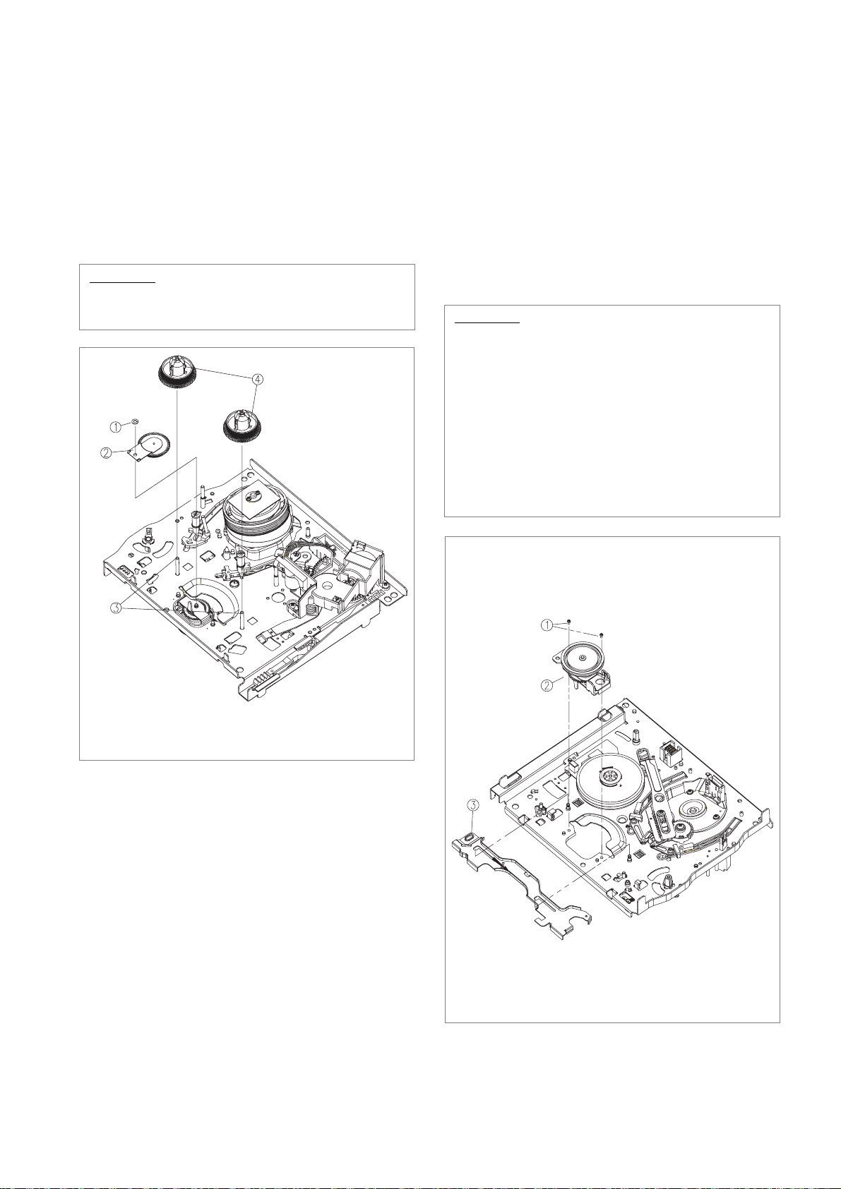
3. 4. Disassembly of LOADING RACK, LOADING
ASS’Y, S/T SLANT POLE ASS’Y (Fig. 3.6, 3.7)
a. Turn out the DECK MECHANISM and remove the
LOADING RACK @ after unscrewing the SCREW .
b. Disintegrate the R LOADING AS # and L LOADING
AS $ .
c. Disintegrate the S SLANT POLE AS % and T SLANT
POLE AS ^ by moving those part in arrow dircetion.
3. 5. Disassembly of the A/C HEAD ASS’Y (Fig. 3.8)
a. Remove the CONNECTOR @ from the AC HEAD
ASS`Y, Watch out that there is no damage in the HEAD
connecting PIN.
b. Separate the AC HEAD ASS`Y ! after unscrewing the-
screw #
DISASSEMBLY AND REPLACEMENT (CONTINUED)
CAUTION:
• Take care GUIDE ROLLER of S/T SLANT POLE AS
and SLANT POLE not to be stained with grease during
assembly.
• Refer to Fig. 3.7 in assembly.
FIg. 3.6 Disassembly of the LOADING RACK, LOADING
ASS’Y and the SLANT POLE ASS’Y
FIg. 3.7 Assembly of the L/R LOADING AS and the
LOADING RACK
CAUTION:
• After the assembly, adjust the tape transmissionsection by refering to the chapter 5.
• After the adjustment of the tape transmission section,
paint the 3 adjustment screw with locking paint.
FIg. 3.8 Disassembly of the AC HEAD ASS’Y
Page 4
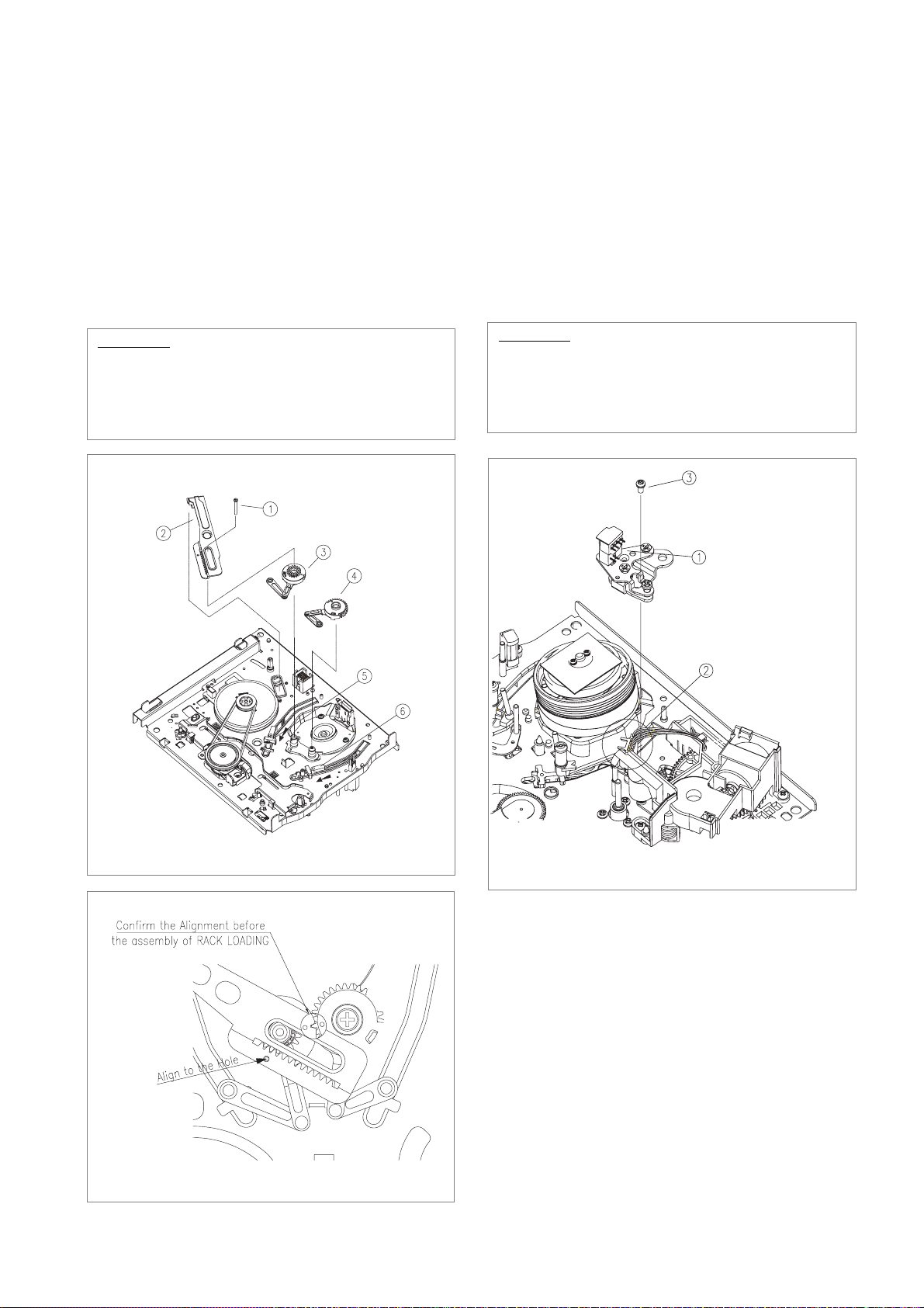
3. 6. Disassembly of the LC BRKT ASS’Y, PINCH
LEVER TOTAL ASS’Y (Fig. 3.9)
a. Separate the LC BRKT Ass’y @ after removing the 3
screws !.
b. Separate the LC BRKT Ass’y @ from the DECK
MECHANISM.
c. Disintegrate the PINCH LEVER TOTAL Ass’y #.
3. 7. Disassembly of the CAM GEAR, RELAY
LEVER, FL RACK (Fig. 3.9)
a. Separate the CAM GEAR % from the MAINBASE.
b. Separate the RELAY LEVER ^ from the MAINBASE.
c. Separate the FL RACK & from MAINBASE by moving
to the arrow direction.
DISASSEMBLY AND REPLACEMENT (CONTINUED)
CAUTION:
• After the assembly of the PINCH LEVER TOTAL
Ass’y, adjust the tape transmission section by refering to
the chapter 5.
• There should be no pollution on the surface of
PINCH ROLLER $ with grease or other foreign
material.
• Make sure if the end of the PINCH SPRINGPINCH
“A” is located at the end of trajectory of CAM GEAR
“B” in assembly (Refer to Fig. 4.3)
CAUTION:
• When reassembling, refer to Fig. 3.10, Fig. 3.11 and
chapter 4.
FIg. 3.9 Disassembly of the LC BRACKET ASS’Y from
the PINCH LEVER TOTAL ASS’Y
FIg. 3.10 Assembly of the CAM GEAR, RELAY LEVER
FIg. 3.11 Assembly of the CAM GEAR, FL RACK
Page 5
3. 8 Disassembly of the S/T BRAKE ASS’Y(Fig. 3.12)
a. Unhook the S BRAKE SPRING # from the MAIN-
BASE HOOK !.
b. Remove the S BRAKE Ass’y @ from the mainbase.
c. Remove the T BRAKE SPRING ^ from the MAIN-
BASE HOOK $.
d. Remove the T BRAKE Ass’y %.
3. 9 Disassembly of the TENSION BAND ASS’Y
(Fig. 3.13)
a. Unhook the TENSION SPRING @ from the MAIN-
BASE HOOK !.
b. Unhook the MAINBASE HOOK “A” and remove the
TENSION BAND Ass’y # from the mainbase.
3. 10 Disassembly of the Capstan Motor (Fig. 3.13)
a. Separate the CAPSTAN MOTOR % after the removal of
3 screws $ holding the capstan motor.
3.11 Disassembly of the FE HEAD (Fig. 3.13)
a. Remove the screw ^ and separate the FE HEAD & from
the MAINBASE.
DISASSEMBLY AND REPLACEMENT (CONTINUED)
CAUTION:
• After the assembly of TENSION BAND Ass’y on the
mainbase, adjust the TENSION POLE location as
shown in Fig. 3.14.
• Avoid getting Grease, Oil or Foreign substance on the
FELT of the BAND BRAKE.
• Take care not to deform the MAINBASE HOOK “A”
when separating the TENSION BAND Ass’y #.
FIg. 3.12 Disassembly of the S/T BRAKE ASS’Y
FIg. 3.13 Disassembly of the TENSION BAND ASS’Y,
CAPSTAN MOTOR and the FE HEAD
FIg. 3.14 Adjustment of the TENSION POLE POSITION
Page 6
3.12 Disassembly of the REEL T ABLE, IDLER
PLA TE T OTAL ASS’Y (Fig. 3.15)
a. Remove the POLY WASHER ! and separate the
IDLER PLATE TOTAL Ass’y @ from the mainbase.
b. Remove the REEL TABLE $ from the REEL TABLE
POST # of the MAINBASE.
3.13 Disassembly of the REEL BRKT TOTAL
ASS’Y, CONNECT PLATE (Fig. 3.16)
a. Turn over the DECK MECHANISM and remove 2
screws !.
b. Remove the REEL BRKT TOTAL Ass’y @ from the
MAINBASE.
c. Separate the CONNECT PLATE # from the MAIN-
BASE by pushing to the direction of the arrow.
DISASSEMBLY AND REPLACEMENT (CONTINUED)
CAUTION:
• Take care not to deform the IDLER PLATE TOTAL
Ass’y @ when assembling and disassembling.
CAUTION:
• In diassembly of the REEL BRKT TOTAL ASS`Y,
take care REEL BELT and REEL FELT not to be
stained with GREASE, OIL, or foreign substance.
• diassembly of the IDLER ASS`Y should be precede
the diassembly of the REEL BRKT TOTAL ASSY.
• Check the operation of the REEL BRKT TOTAL
ASSY before assembly.
• Check the operation of FF/REW, PLAY, CUE, and
REVIEW work well and existence of noise during
the mode operation..
FIg. 3.15 Disassembly of the REEL TABLE and the IDLER
PLATE TOTAL ASS’Y
FIg. 3.16 Disassembly of the REEL BRKT TOTAL ASS’Y
and the CONNECT PLATE
Page 7
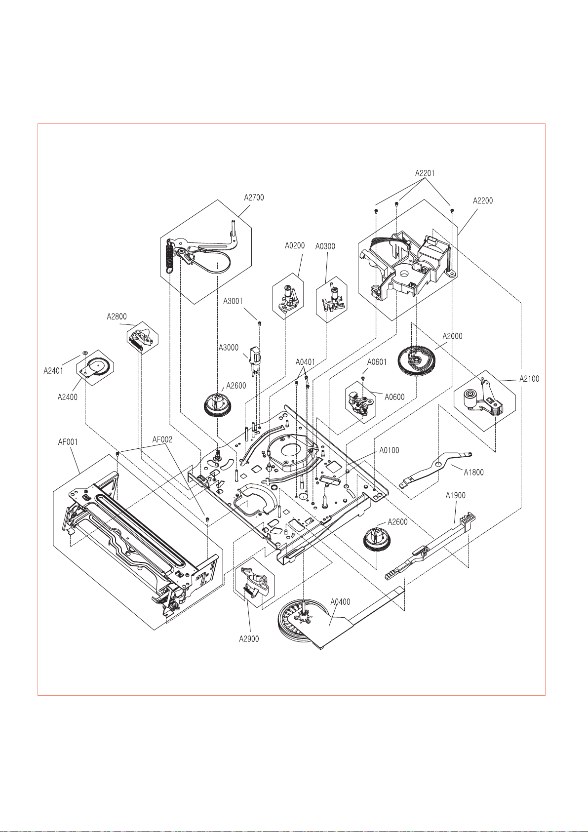
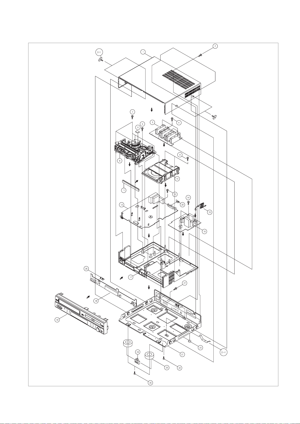
6.1 Exploded view of DECK Ass’y ( Top View)
6. EXPLODED VIEW
Page 8
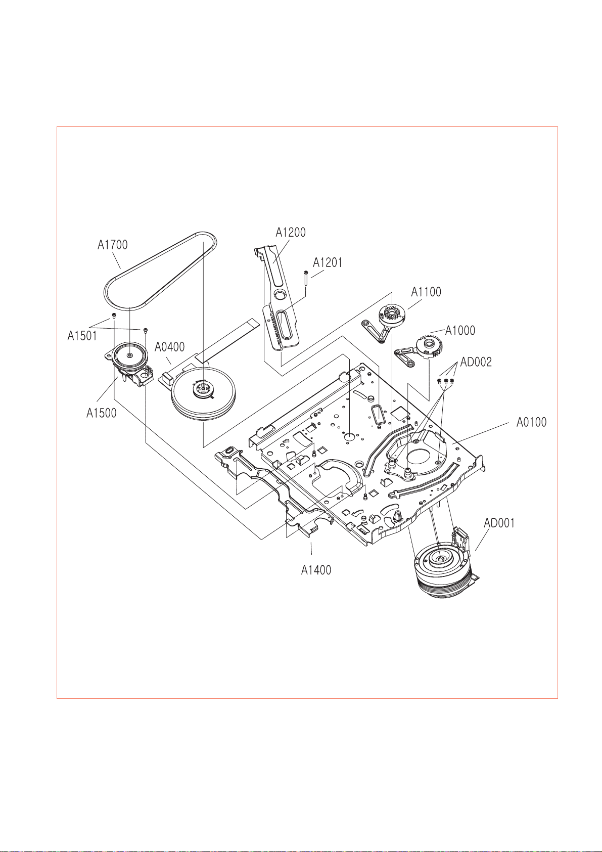
6. 2 Exploded view of DECK Ass’y ( Bottom View)
EXPLODED VIEW (CONTINUED)
Page 9
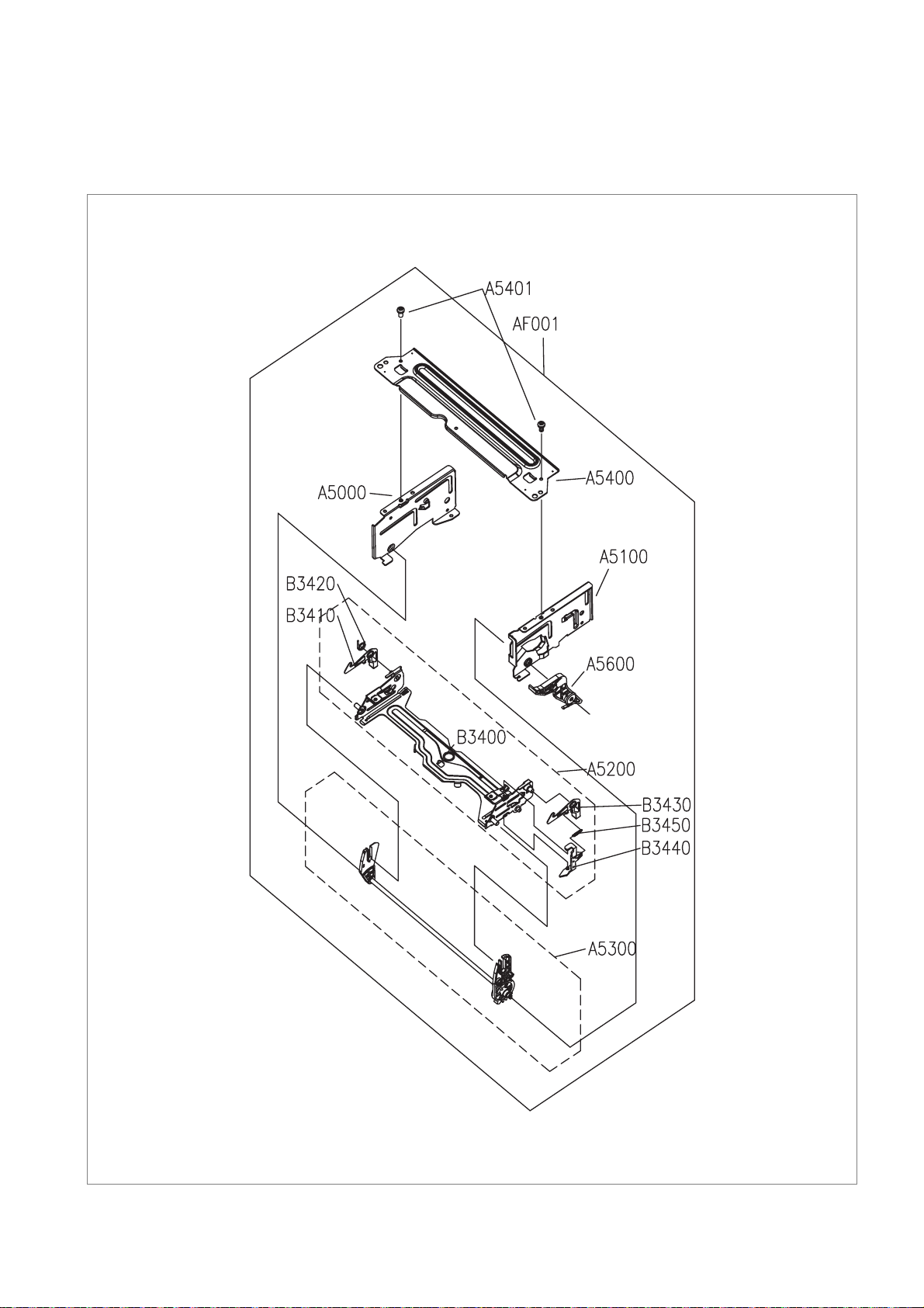
6.3 Exploded view of FL Ass’y
EXPLODED VIEW (CONTINUED)
Page 10
D0040
D0040
D0020
D0050
D0010
D0060
D0070
Page 11
Page 12
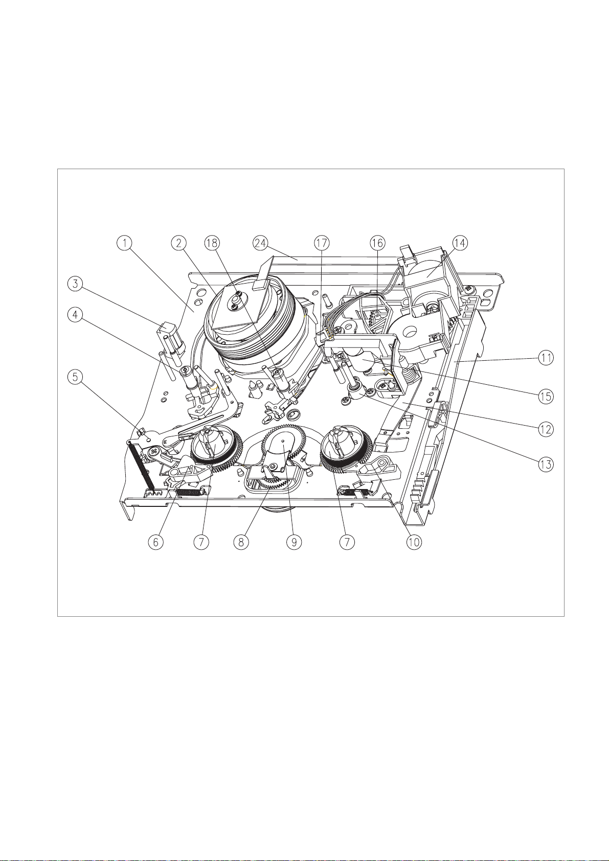
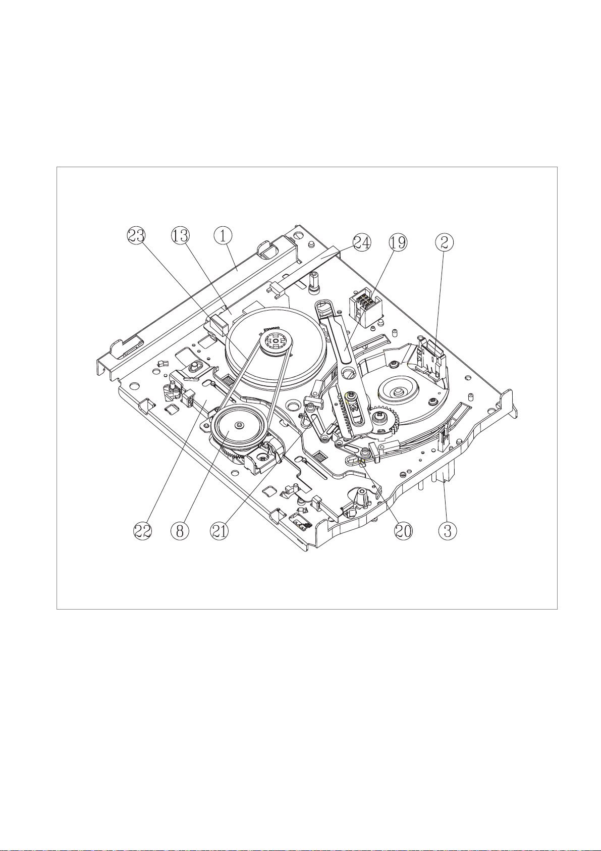
2.1. Assembly diagram
2.1.1. DECK Assembly diagram
A. Upper View
2. ASSEMBLY DIAGRAM AND A/S
1MAIN BASE ASS’Y
2 DRUM ASS’Y
3 FE HEAD
4 S SLANT POLE ASS’Y
5 TENSION BAND ASS’Y
6 S BRAKE ASS’Y
7 REEL TABLE
8 REEL BRKT TOTAL ASS’Y
9 IDLER PLATE TOTAL ASS’Y
10 T BRAKE ASS’Y
11 FL RACK
12 RELAY LEVER
13 CAPSTAN MOTOR
14 LC BRKT ASS’Y
15 PINCH LEVER TOTAL ASS’Y
16 CAM GEAR
17 AC HEAD ASS’Y
18 T SLANT POLE ASS’Y
19 LOADING RACK
20 L LOADING ASS’Y
21 R LOADING ASS’Y
22 CONNECT PLATE
23 REEL BELT
24 CABLE FFC
Page 13
ASSEMBLY DIAGRAM AND A/S(CONTINUED)
B. Lower V iew
1MAIN BASE ASS’Y
2 DRUM ASS’Y
3 FE HEAD
4 S SLANT POLE ASS’Y
5 TENSION BAND ASS’Y
6 S BRAKE ASS’Y
7 REEL TABLE
8 REEL BRKT TOTAL ASS’Y
9 IDLER PLATE TOTAL ASS’Y
10 T BRAKE ASS’Y
11 FL RACK
12 RELAY LEVER
13 CAPSTAN MOTOR
14 LC BRKT ASS’Y
15 PINCH LEVER TOTAL ASS’Y
16 CAM GEAR
17 AC HEAD ASS’Y
18 T SLANT POLE ASS’Y
19 LOADING RACK
20 L LOADING ASS’Y
21 R LOADING ASS’Y
22 CONNECT PLATE
23 REEL BELT
24 CABLE FFC
Page 14
ASSEMBLY DIAGRAM AND A/S(CONTINUED)
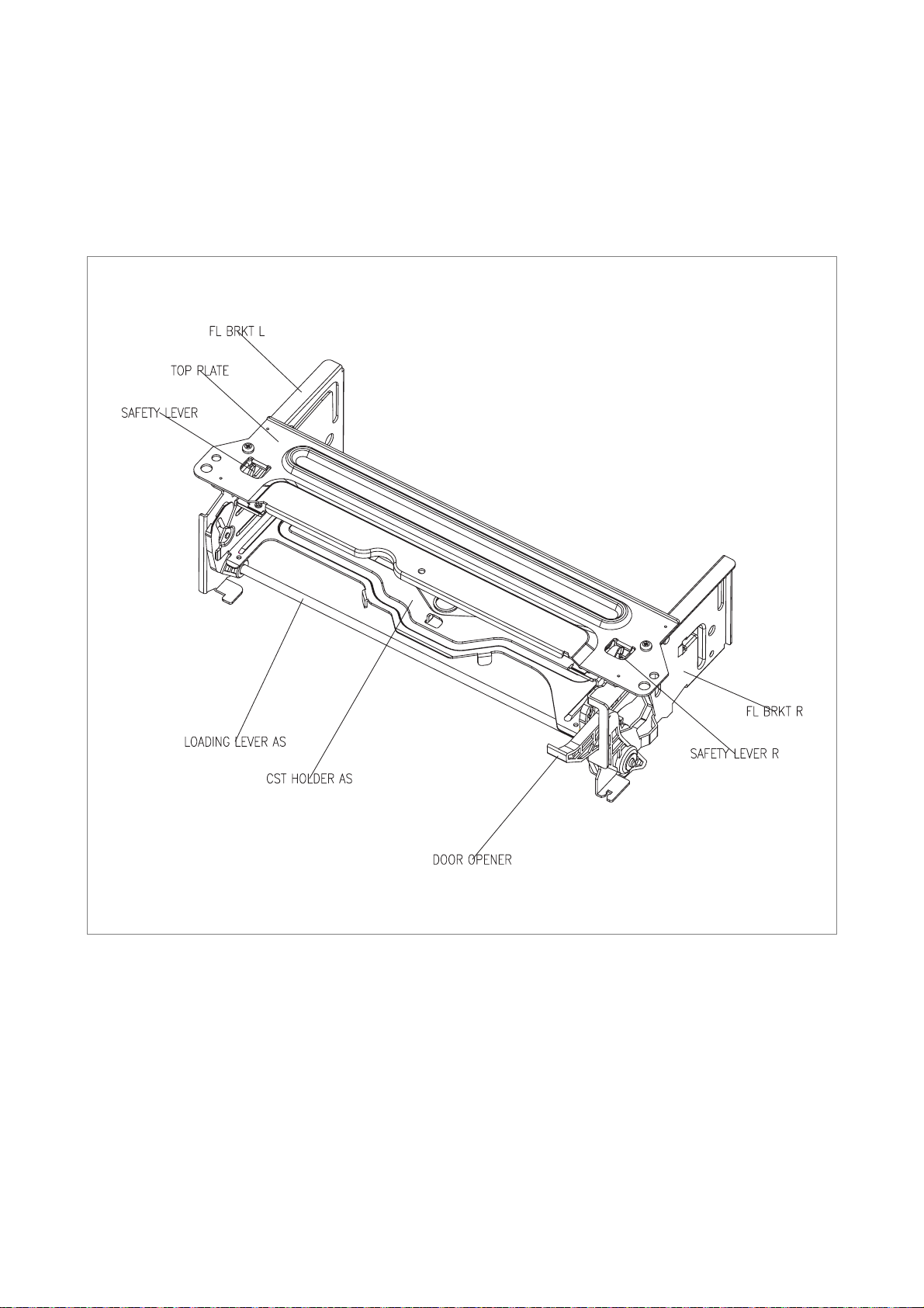
2.1.2. FRONT LOADING Assembly diagram
1 FL BRKT L
2 TOP PLATE
3 SAFETY LEVER
4 LOADING LEVER AS4
5 CST HOLDER AS
6 DOOR OPENER
7 SAFETY LEVER R
8 FL BRKT R
Fig.2
Page 15
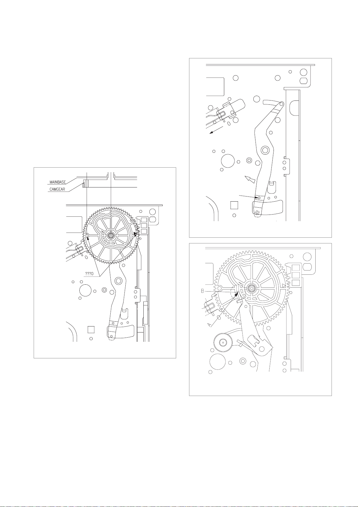
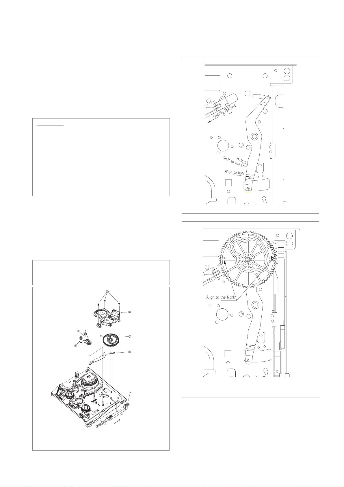
4. 1 Mechanical Adjustment (Fig. 4.1~4.4)
In case of diassembly and reassembly for fixing the mecanical
problem, check the following check point.
a. Make sure that the DATUM HOLE of the CAM GEAR is
aligned wth the DATUM HOLE in the MAINBASE in
the EJECT mode as shown in Fig. 4-1.
b. Make sure that the ending part “A” of the RELAY
LEVER assembled on the CONNECT PLATE is aligned
with the reference hole “B” of the MAINBASE as shown
in Fig. 4.2.
c. The end point “A” of PINCH SPRING PIN of the
LEVER TOTAL ASS`Y should be located within the
trajectory “B” of the CAM GEAR. (Fig. 4.3)
4. MECHANICAL ADJUSTMENT
FIg. 4.1 Assembly reference between the FL RACK and the
CAM GEAR
TURN TO THE END
ALIGN
FIg. 4.2 Assembly reference between the RELAY LEVER
and the CAM GEAR
FIg. 4.3 Assembly reference of the PINCH LEVER TOTAL
ASS’Ywith the CAM GEAR
Page 16
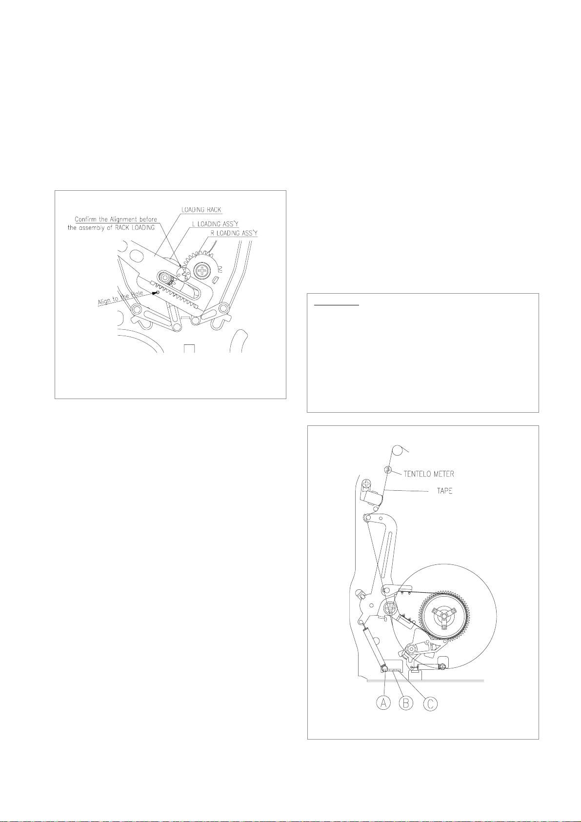
d. Make sure that the triangular mark “A” of the L LOAD-
ING Ass’y is aligned with the mark “b” of the R LOADING Ass’y. (Fig. 4.4)
e. Reference hole “C” of the LOADING RACK should be
aligned with the reference hole of the R LOADING Ass’y
to make the teeth of the LOADING RACK is aligned as
shown in Fig. 4.4.
4. 2 Adjustment and measurement of the BACK
TENSION (Fig. 4.5, 4.6)
a. Check that the location of the TENSION POLE is in the
right position. if not, adjust that by refering to the “4.4
Adjustment of the TENSION POLE position”.
b. Play back the T-120 TAPE in S-MAX for 20
seconds.(Generally tape transporting section is settled
down in 20 seconds)
c. Measure the BACK TENSION by using the TENTELO
METER (Refer Fig 4.5) The result should be within the
range of 20g ~ 30g.
d. If the BACK TENSION is out of the range, change the
position of the TENSION SPRING of repeat the
process of “4.4 Adjustment of the TENSION POLE
position”.(Fig. 4.6)
MECHANICAL ADJUSTMENT (CONTINUED)
FIg. 4.4 Assembly reference between the LOADING RACK
and the LOADING LEVER ASS’Y
CAUTION:
• If the measurement result greater than the upper limit,
change the hook point of the spring to position “A”
• Confirm that all of the three probes of TENTELO
METER are in contect with the tape.
• During measuring, don`t touch any other parts of the
MECHANISM(i.e. MAINBASE). It is recommended that this measurment be repeated at least three
times for an accurate reading.
FIg. 4.5 Measurement of the BACK TENSION
Page 17
4. 3 Mechanical Mode (Operate without a cassette
tape)
a. Remove the FRONT LOADING MECHANISM from the
DECK MECHANISM
b. Cap the IR LED and pull the FL RACK. This has the same
effect with cassette loading to the deck.
c. If the S,T POLE BASE is loaded, PLAY MODE starts
automatically. If you want other function, press the corresponding button.
d. Turn off the power when the Mechanism is in the desired
position.
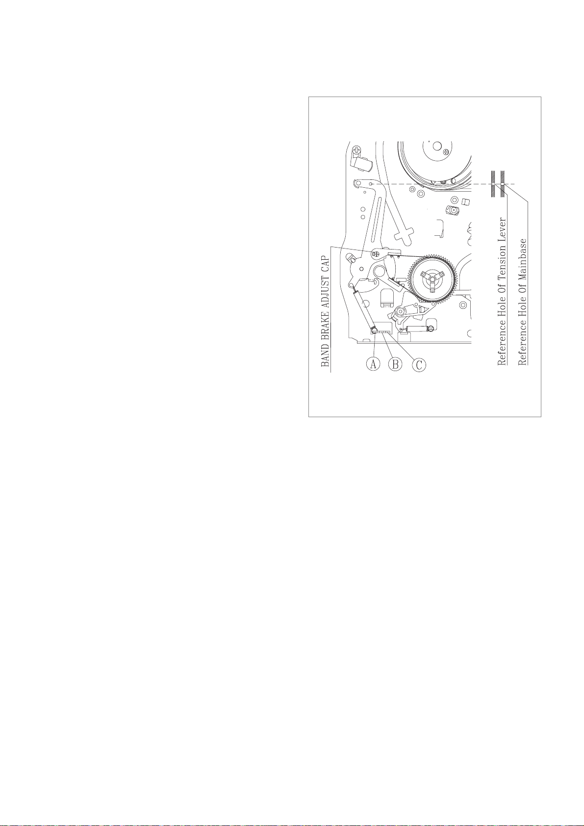
4. 4 Adjustment of the position of the TENSION
POLE (Fig. 4.6)
a. Place the MECHANICAL MODE in the PLAY MODE.
Refer to the above section “4.3 MECHANICAL MODE”
b. Confirm that the TENSION LEVER is aligned with the
datum hole of the MAINBASE.
c. If the requirement “b” is not satisfied. turn the BAND
BRAKE ADJUST CAP clockwise or counterclockwise
until the two datum holes aligns with each other.
MECHANICAL ADJUSTMENT (CONTINUED)
FIg. 4.6 Adjustment of the TENSION POLE POSITION
Page 18
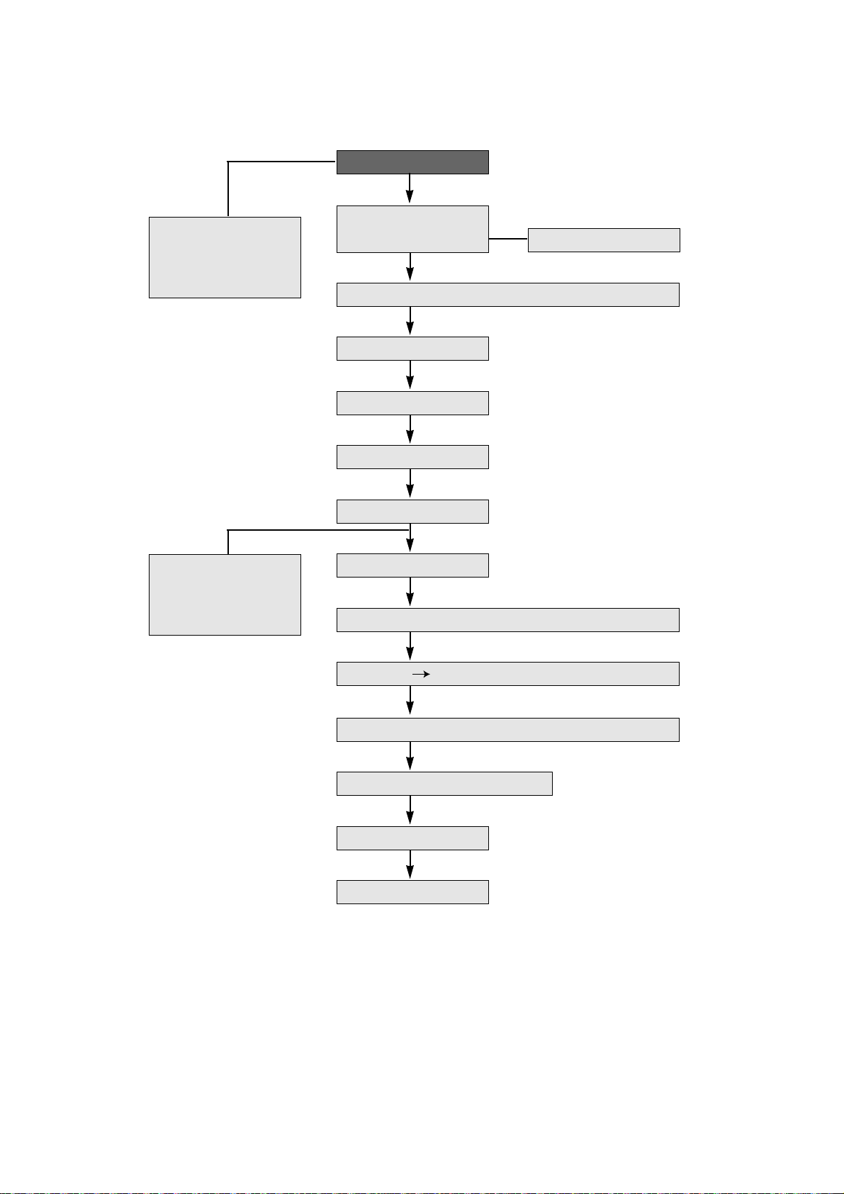
5. ADJUSTMENT OF THE TAPE TRANSPORT SECTION.
Generally, tape transporting section has been precisely adjusted in the factory and does not require the ordinary readjustment.
But there is the case that tape noise or impact on the deck mechanism, tape transporting section readjustment is required. In
adjustment of the tape transmission section consut the following flow chart.
If any components shown in Fig. 5.1, tape transport section are changed. To readjust the tape transporting section.
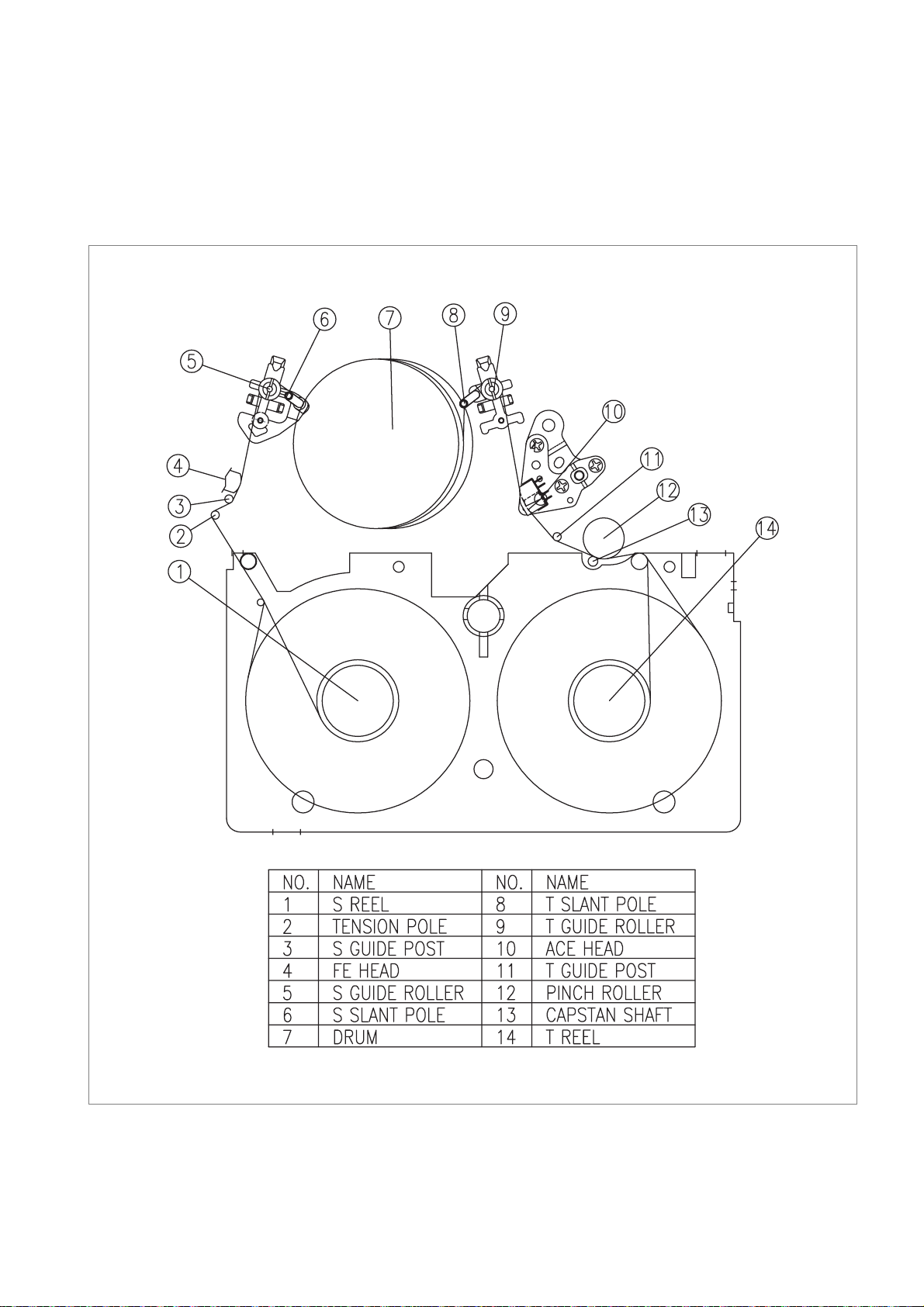
FIg.5.1 A schematic diagram of the tape transport ing section.
Page 19
S/T GUIDE ROLLER HEIGHT
ADJUSTMENT
•DRUM TOTAL AS
•A/C HEAD AS
•PINCH LEVER TOTAL
AS
S/T GUIDE ROLLER FLUNGE
A/C HEAD AS ADJUSTMENT (TILT ADJUSTMENT)
CLEANING
AUDIO AZIMUTH ADJUSTMENT
A/C HEAD ADJUSTMENT
X-POSITION ADJUSTMENT
PLAYBACK PHASE ADJUSTMENT
LINEARITY ADJUSTMENT
DRUM ENTRANCE/EXIT ENVELOPE FINE TUNING
REVIEW PLAY CHANGING OPERATION CHECK
AUDIO AZIMUTH ADJUSTMENT
AUDIO OUTPUT CHECK (A/C HEAD HEIGHT& TILT ADJUSTMENT)
X-POSITION ADJUSTMENT
TRACKING
•S SLANT PLOE AS
•T SLANT POLE AS
•TENSION BAND AS
Table.1 Adjustment Flow Diagram of the Tape Transporting System
Page 20
A. Adjustment of the S/T GUIDE ROLLER
A. Adjustment of the S/T GUIDE ROLLER
a. Check the Playing back with a T-120 TAPE.
b. Make sure that excessive tape wrinkle does not occure
ateatch S, T GUIDE ROLLER.
c. If tape wrinkle is observed at the S/T GUIDE ROLLER,
turn the guide roller screw until there is not tape wrinkle.
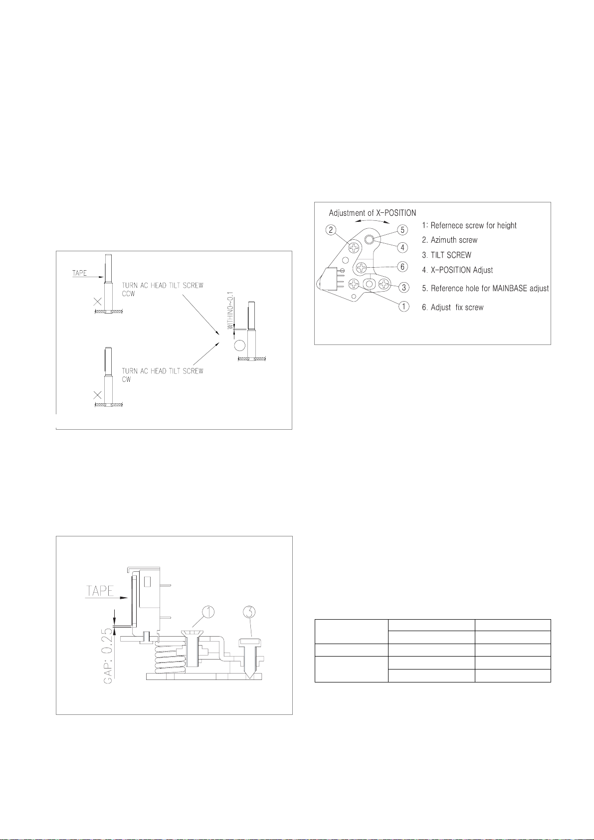
B.Adjustment of the AC HEAD ASS’Y(TILT)
a. Play back a T-120 TAPE and check the running status of
lower side of GUIDE POST.
b. If there is any problem, Turn the AC HEAD TILT
SCREW until the running status improved. (Fig. 5.2)
C.Adjustment of the AC HEAD Height(Fig. 5.3)
a. Play back a T-120 TAPE..
b. Make sure that the gap between the lower end of TAPE
and the AC head is 0.25m.
c. If the measurement of the gap is different from the refer-
ence value 0.25mm, turn the screw ! , # until the
desired gap is obtained.
D.Adjustment of the AUDIO AZIMUTH(Fig. 5.4)
a. Play back the ALIGNMENT TAPE
(DN2 : SP, NTSC,7KHz)
b. Check the AUDIO output with a AUDIO LEVEL
METER.
c. Turn the AC HEAD AZIMUTH SCREW @ until the
maximum AUDIO output(-9dBm ~ -3dBm)is obtained.
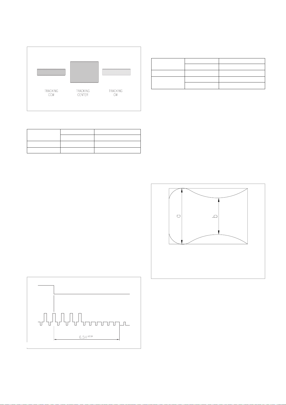
E.Adjustment of the X-POSITION(Fig. 5.4 5.5)
a. Connect the PATH ADJ. FIXTURE to the PT01 on the
MAIN CIRCUIT BOARD.
b. Play back the ALIGNMENT TAPE (DN2 : SP MONO-
SCOPE).
c. Connect the S/W pin and ENVE pin of the PATH ADJ.
FIXTURE with the SCOPE PROBE.
d. Insert the adjustment bar in the AC HEAD ADJUST hole
$ and adjust the X-POSITION of the AC HEAD
ASS`Y until the ENVE is maximum when the VR is on
the CENTER.
• There is the possibility that an another TRACKING CENTER can be occur when the AC HEAD ASS`Y turned
completely in the counterclockwise direction, Hence adjust
the X-position with AC HEAD ASS’Y adhering closely
to the right side until the maximum ENVE is obtained.
e. The adjustment of the X-POSITION finished, check
if the AUDIO LEVEL is degraded, then readjustment
of the AUDIO AZIMUTH is required.
ADJUSTMENT OF THE TAPE TRANSPORT SECTION. (CONTINUED)
FIg.5.2 Adjustment of the AC HEAD ASS’Y
FIg.5.3 Adjustment of AC HEAD Height
FIg.5.4 Adjustment of AUDIO AZIMUTH, X-POSITION
S/W PULSE TEST PIN PATH ADJ. FIXTURE
ENVELOPE TEST PIN PATH ADJ.FIXTURE
Measurement Equipment OSILLOSCOPE
VR CONTROL PATH ADJ.FIXTURE
AC HEAD ADJUST HOLE ADJUSTMENT BAR
Test Point
Adjustment
Page 21
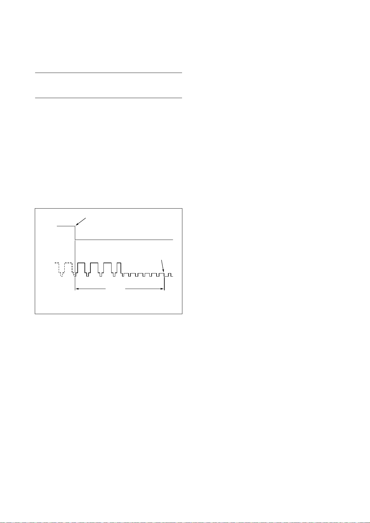
F. PLAYBACK PHASE ADJUSTMENT(Fig. 5.6)
PHASE GENERATOR(PG) SHIFTER determine the
VIDEO HEAD SWITCHING POINT when the TAPE is
played back. If an adjustment of the PHASE GENERATOR(PG) SHIFTER is not done precisely, There can be a
HEAD SWITCHING NOISE or a VERTICAL JITTER
problem, vibration of the picture on the screen, not good
quality of picture in special play back.
a. Connect the PT01 on the MAIN CIRCUIT BOARD with
a PATH ADJ. FIXTURE.
b.
Play back an ALIGNMENT TAPE(DN-2 : MON-SCOPE signal)
c. Connect the S/W PULSE TEST PIN on the PATH ADJ.
FIXTURE with a CHANNEL-1 SCOPE PROBE.
d. Connect the VIDEO OUT on the MAIN CIRCUIT
BOARD with a CHANNEL-2 SCOPE PROBE (1V/div).
e. Control the PG VOLUME until the time interval
between the SWITCHING PULSE and the V-SYNC
SIGNAL is within the 6.5H±0.5H as shown in Fig. 5.6.
G.Adjustment of the LINEARITY(Fig. 5.7)
a. Connect the PT01 on the MAIN CIRCUIT BOARD with
a PATH ADJ. FIXTURE.
b. Play back an ALIGNMENT TAPE(DN-2 : MONO-
SCOPE Signal).
c. Connect the FIXTURE S/W PULSE TEST PIN on the
PATH ADJ. CHANNEL-1 SCOPE PROBE.
d. Connect the VIDEO OUT on the MAIN CIRCUIT
BOARD with a CHANNEL-2 SCOPE PROBE (1V/div).
e. Adjust the VR CONTROL on the ADJ. FIXTURE until
the ENVELOPE signal is maximum while play back the
ALIGNMENET TAPE.
f. Adjust the S/T GUIDE ROLLER until the envelope signal
waveforms of the entrance and exit sides are as shown in
Fig. 5-7.
ADJUSTMENT OF THE TAPE TRANSPORT SECTION. (CONTINUED)
FIg.5.5 Adjustment of the X-POSITION
S/W PULSE TEST PIN PATH ADJ. FIXTURE
ENVELOPE TEST PIN PATH ADJ.FIXTURE
Measurement Equipment OSILLOSCOPE
VR CONTROL PATH ADJ.FIXTURE
S/T GUIDE ROLLER TAPE TRANSPORT SECTION
Test Point
Adjustment
a: Max Output of Envelope
b: Min Output of Envelope
FIg.5.7 Adjustment of Linearity
Fig.5.6 Playback Phase Adjustment
S/W PULSE TEST PINMAIN CIRCUT BOARD
ENVELOPE TEST PINMAIN CIRCUT BOARD
Measurement Equipment OSILLOSCOPE
VR 595(PG SHIFTER)MAIN CIRCUT BOARD
Test Point
Adjustment
Page 22
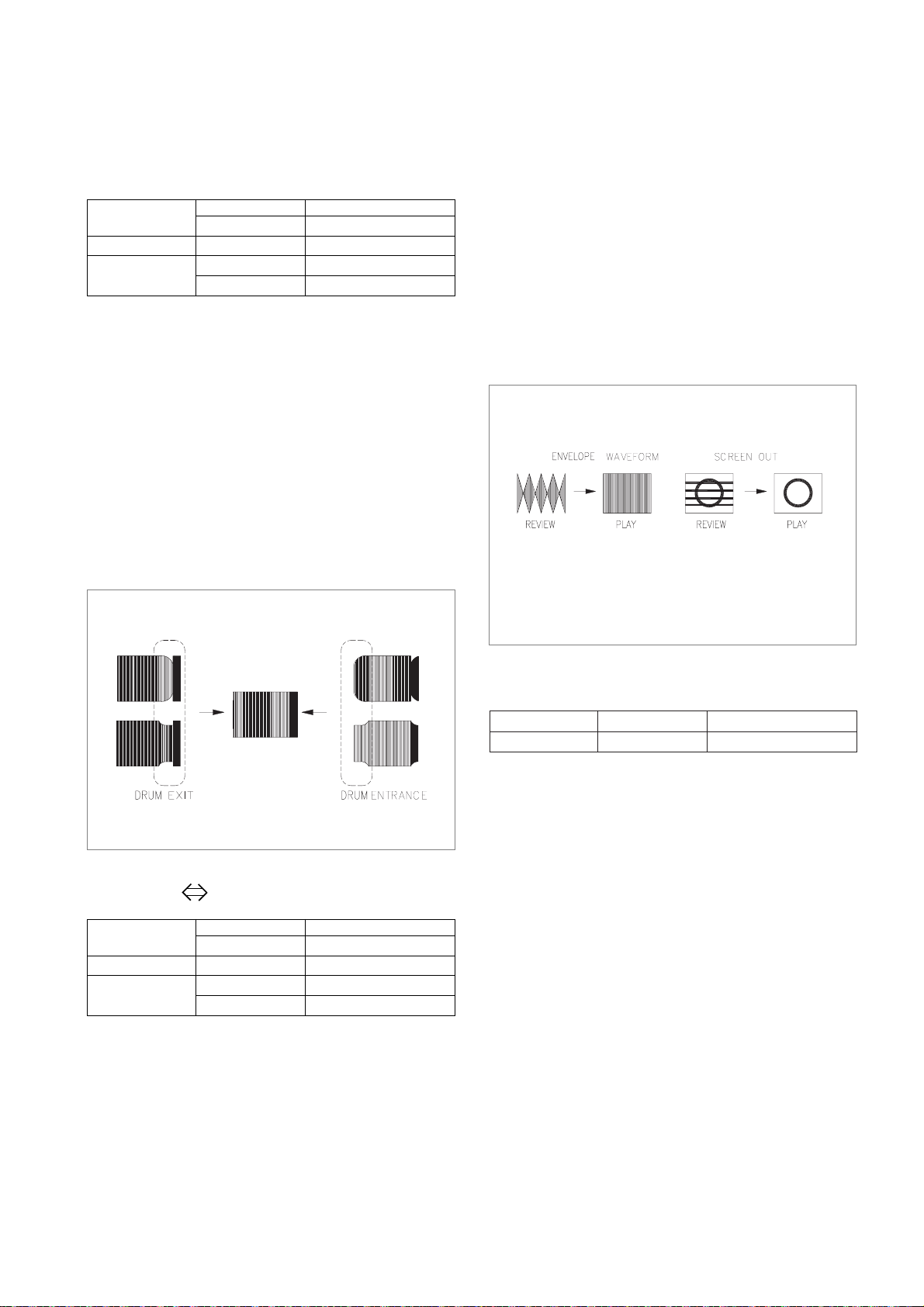
H. Adjustment of the wave form of DRUM Entrance
/ Exit (Fig. 5.8)
a. Connect the PT01 on the MAIN CIRCUIT BOARD with
a PATH ADJ.FIXTURE.
b. Play back an ALIGNMENT TAPE(DN-2 : MONO-
SCOPE signal)
c. Connect the S/W PULSE TEST PIN on the PATH ADJ.
FIXTURE with a CHANNEL-1 SCOPE PROBE.
d. Connect the VIDEO OUT on the MAIN CIRCUIT
BOARD with a CHANNEL-2 SCOPE PROBE(1V/div).
e. Turn the VR CONTROL on the PATH ADJ.FIXTURE
clockwise or counterclockwise until the signal shape of
ENVELOPE has the constant thickness.(Fig.5.8)
f. Adjust the S/T GUIDE ROLLER if the thickness of the
ENVELOPE signal is not uniform.
I. REVIEW PLAY(Fig. 5.9)
a. Connect the PT01 on the MAIN CIRCUIT BOARD with
a PATH ADJ.FIXTURE.
b. Play back an ALIGNMENT TAPE(DN-2 : MONO-
SCOPE signal)
c. Connect the S/W PULSE TEST PIN on the PATH ADJ.
FIXTURE with a CHANNEL-1 SCOPE PROBE.
d. Connect the VIDEO OUT on the MAIN CIRCUIT-
BOARD with a CHANNEL-2 SCOPE PROBE (1V/div).
e. Make the VR CONTROL on the PATH ADJ. FIXTURE
to the center to maximize the ENVELOPE signal.
f. Play back the REVIEW mode about 15 second and alter
the mode to PLAY MODE.
g. Check whether the ENVELOPE waveform restore to its
original form within 3 second when the REVIEW mode is
changed to PLAY mode.
h. If the requirement of “g” is not satisfied, Check the run-
ning status of tape on the lower part of T GUIDE POST
and adjust the S/T GUIDE ROLLER precisely
.
J.Checking AUDIO output waveform (Adjustment
of AC HEAD TILT & Height)
a. Connect the AUDIO output jack with an AUDIO LEVEL
METER.
b. Playback an Alignment Tape (DN-1:Color Bar 1KHz
Signal)
c. Check if the AUDIO output signal level is over -9~-
3dBm.
d. If the requirement of “c” is not satisfied, readjust the AC
HEAD TILT and the HEIGHT until the AUDIO output is
maximized. (Fig. 5.2, 5.3)
ADJUSTMENT OF THE TAPE TRANSPORT SECTION. (CONTINUED)
S/W PULSE TEST PIN PATH ADJ. FIXTURE
ENVELOPE TEST PIN PATH ADJ.FIXTURE
Measurement Equipment OSILLOSCOPE
VR CONTROL PATH ADJ.FIXTURE
S/T GUIDE ROLLER TAPE TRANSPORT SECTION
Test Point
Adjustment
FIg.5.8 Fine adjustment of the ENVELOPE at the DRUM
ENTRANCE/EXIT
S/W PULSE TEST PIN PATH ADJ. FIXTURE
ENVELOPE TEST PIN PATH ADJ.FIXTURE
Measurement Equipment OSILLOSCOPE
VR CONTROL PATH ADJ.FIXTURE
S/T GUIDE ROLLER TAPE TRANSPORT SECTION
Test Point
Adjustment
FIg.5.9 Waveform change when the modealtered
(REVIEW ↔PLAY)
AUDIO OUTPUT AUDIO OUTPUT JACK
AUDIO LEVEL METER
Test Point
Measurement Equipment
Page 23

K.Adjustment of the AUDIO AZIMUTH
a. Connect the AUDIO output JACK with an AUDIO
LEVEL METER.
b. Play back the ALIGNMENT TAPE(DN-2:MONO-
SCOPE 7KHz Signal).
c. Check if the AUDIO output signal level is over : -9 ~-
3dBm.
d. If the requirement of “c” is not satisfied, readjust the
AZIMUTH SCREW of the AC HEAD until the AUDIO
output is maximum.(Fig. 5.4)
e. Repeat the process of “Adjustment of the wave form of
DRUM Entrance/Exit”
L.X-POSITION
a. Connect the PT01 on the MAIN CIRCUIT BOARD with
a PATH ADJ. FIXTURE.
b. Play back an ALIGNMENT TAPE(DN-2 : MONO-
SCOPE Signal).
c. Connect the S/W PULSE TEST PIN on the PATH ADJ.
FIXTURE with a CHANNEL-1 SCOPE PROBE.
d. Connect the VIDEO OUT on the MAIN CIRCUIT
BOARD with a CHANNEL-2 SCOPE PROBE (1V/div).
e. Check if the ENVELOPE is maximum when the VR
CONTROL on the PATH ADJ. FIXTURE is in CENTER
f. If the requirement “e” is not satisfied, readjust the X-POSI-
TION by referring to subitem “E”(Adjustment of the XPOSITION).
g. Repeat the process of subitem “F”(PLAYBACK PHASE
ADJUSTMENT).
ADJUSTMENT OF THE TAPE TRANSPORT SECTION. (CONTINUED)
AUDIO OUTPUT AUDIO OUTPUT JACK
AUDIO LEVEL METER
Test Point
Measurement Equipment
S/W PULSE TEST PIN PATH ADJ. FIXTURE
ENVELOPE TEST PIN PATH ADJ.FIXTURE
Measurement Equipment OSILLOSCOPE
VR CONTROL PATH ADJ.FIXTURE
S/T GUIDE ROLLER
TAPE TRANSMISSION T SECTION
Test Point
Adjustment
Page 24
ELECTRICAL ADJUSTMENT
Fig. 1 Main board test point/control location guide(component)
RTD300
Page 25
ELECTRICAL ADJUSTMENT
PG (Pulse Generator) Shifter Adjustment (Fig. 3)
Test Points: PT01 PIN # Main
Video Out Jack Rear Panel
Adjust: REC SWITCH Main
The Pulse Generator (PG) Shifter determines the video head
switching point during playback. Misadjustment of the PG
Shifter may cause head switching noise in the picture and/or vertical jitter.
1. Load the instrument with an alignment tape and play back
the color bar signal or monoscope signal.
2. Connect Path Fixture to PT01.
3. Connect channel-1 scope probe (1V/div.: 50µ sec/div.) to
PT01 PIN #. Trigger the scope on channel-1.
4. Connect channel-2 scope probe (1V/div.) to the Video Out
Jack.
5. Set the scope to (-) slope and press the REC SW, the alignment is performed automatically. Confirm that the trailing
edge of the SW 30Hz pulse is placed 6.5H±0.5H (horizontal)
lines before the start of vertical sync pulse.
SWITCHING
SW30Hz
PULSE
VIDEO
OUTPUT
V. SYNC
6.5H–0.5
Fig. 3 - Automatic PG Shifter Adjustment
Page 26
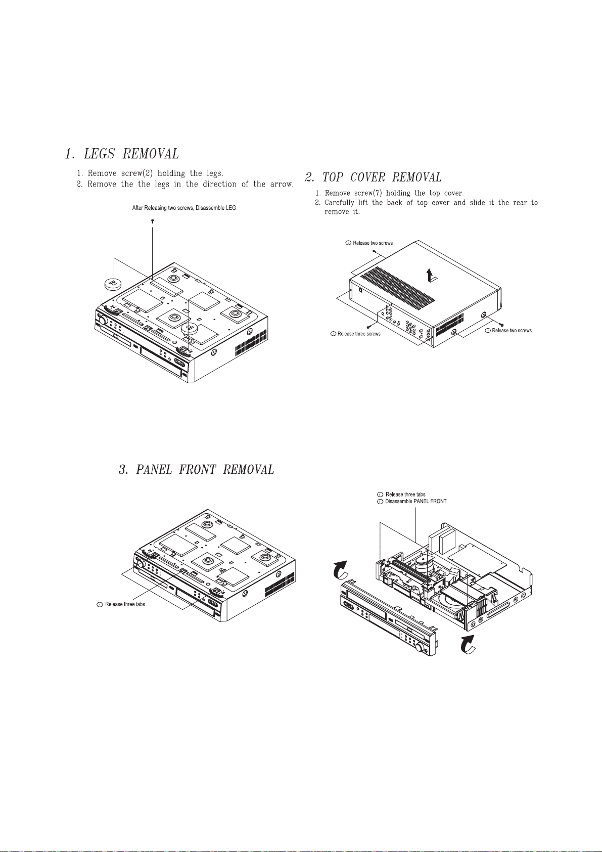
Fig. 1 - Legs Removal
Fig. 2 Top Cover Removal
INSTRUMENT DISASSEMBLY
Perform all disassembly procedures in the order presented. When reassembling, use the reverse procedure. Make sure that all
leads/wiring are routed correctly when reassembling.
PRT_CSYS_DEFyyDEFAULT
zz
xx
Fig. 3 . Panel Front Removal
Page 27
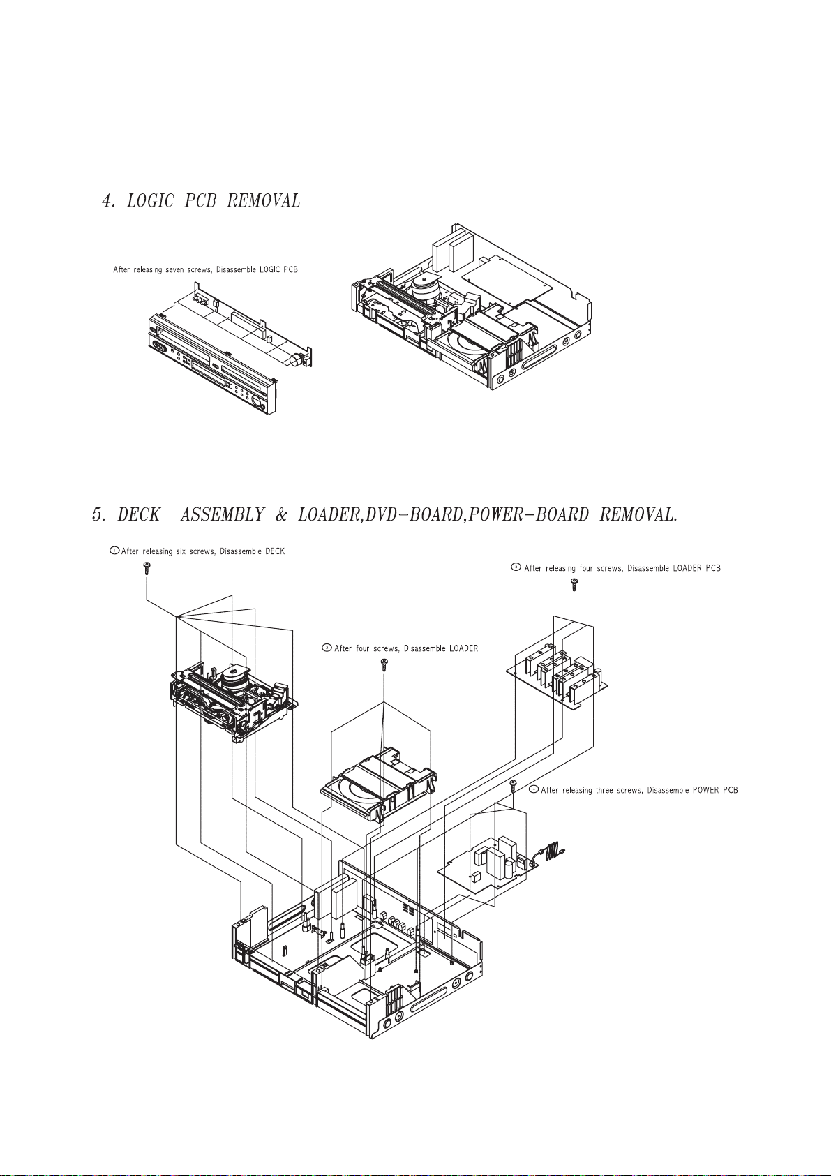
INSTRUMENT DISASSEMBLY (Continued)
Fig. 5 . DECK & LOADER,POWER BOARD Removal
Fig. 4 . LOGIC PCB Removal
Page 28
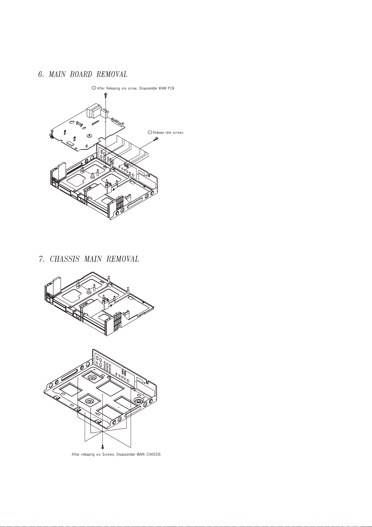
INSTRUMENT DISASSEMBLY (Continued)
Fig. 6. Main Board Removal
Fig. 7. Chassis Main Removal
Page 29
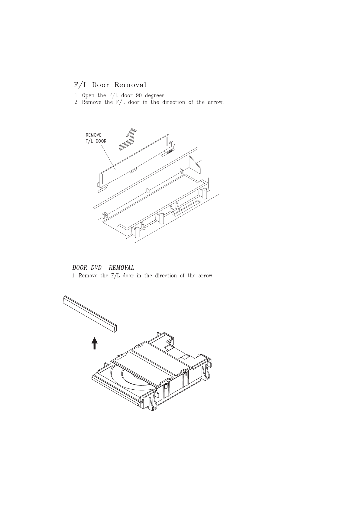
INSTRUMENT DISASSEMBLY (Continued)
Page 30

ABBREVIATIONS
A A or AUD : Audio
A.E. : Audio Erase
AC : Alternating current
ACC : Automatic Color Control
ACS : Auto Clock Set
AFC : Automatic Frequency Control
AFT : Automatic Fine Tuning
AGC : Automatic Gain Control
ALC : Automatic Level Control
AM : Amplitude Modulation
AMP : Amplifier
ANT : Antenna
APC : Automatic phase control
ASS'Y or AS : Assembly
AUTO : Automatic
AV or A/V : Audio/Video
B B : Base, Burst
BAL : Balance
BGP : Burst Gate Pulse
BPF : Bandpass Filter
BW or B/W : Black and White
C C : Capacitor, Chroma, Collector
C Rotary : Color Rotary
C-Sync : Composite Synchronization
CA : Commercial Advance
CAP : Capstan
CAR : Carrier
CATV : Cable Television
CBC : Cable Box Control
CCD : Charge Coupled Devices
CFG : Capstan Frequency Generator
CH : Channel
CHAR : Character
CHROMA : Chrominance
CLK : Clock
CNR : Color Noise Reduction
COMB : Comb Filter
COMP : Comparator, Composite, Compensation
CONV : Converter
CST : Cassette
CTL : Control
CUR : Current
CV : Composite Video
D D : Drum, Digital, Diode, Drain
DC : Direct Current
DD : DC-DC Convert
DEEM or DEEMPH
: Deemphasis
DEMOD : Demodulator
DET : Dectector
DEV : Deviation
DFG : Drum Frequency Generator
DOC : Dropout Compensator
DS : Drain and Source
DSSC : Digital Satellite Set Control
dB : Decibel
E EDS : Extended Data System
ENVE : Envelope
E/V : Envelope/Vertical Sync
G GEN : Generator
GND : Ground
H H : High, Horizontal
HA or HEAD AMP
: Head Amplifier (PreAmp)
HD : Horizontal Drive, Head
HOR : Horizontal
HZ : Hertz
I I/O : Input/Output
IC : Intergrated Circuit
IF : Intermediate Frequency
INS : Insertion
IR : Infrar Red
K KIL : Killer
L L : Low, Left, Coil
LIM : Limit
LM : Loading Motor
LP : Long Play
LPF : Low Pass Filter
M MA : Movie Advance
MAX : Maximum
MIN : Minimum
MIX : Mixer, Mixing
MMV : Monostable Multivibrator
MOD : Modulation, Modulator
MPX : Multiplex
M/T or MTR : Motor
N NC : None Connection
NC or NOICAN : Noise Canceller
NL : None linear
NR : Noise Reduction
O OSC : Oscillator, Oscillation
OSD : On Screen Display
OSP : On Screen Program
OTR : One Touch Record
P P-P : Peak-to-Peak
PB : Playback
PC : Photo Coupler
PCB : Printed Circuit Board
PG : Phase Generator
Page 31

PIC : Picture
PIF : Picture Intermediate Frequency
PLL : Phase Locked Loop
PS : Phase Shift
PWM : Pulse Width Modulator
PWR : Power
Q Q : Transistor
QV : Quasi Vertical
R R : Resistor, Right
REC : Recording
REF : Reference
REG : Regulated, Regulator
REMOCON : Remote Control (Unit)
REV : Reverse
REW : Rewind
RF : Radio Frequency
ROT : Rotary
S SEP : Separation
SHARP : Sharpness
SI or S IN : Serial Input
SO or S OUT : Serial Output
SP : Standard Play
STB : Strobe
SVC : Service
SW or S/W : Switch or Switching Pulse
SYNC : Synchronization
SYSCON : System Control
T TJ : Test Jump
TP : Test Pin
TR : Transistor
TRANS : Transformer
TRK : Tracking
TU : Tuner
U UHF : Ultra High Frequency
V V : Volt, Vertical
V-SYNC : Vertical Synchronization
VCA : Voltage Controlled Adjustor
VCO : Voltage Controlled Oscillator
VCR : Video Cassette Recorder
VD : Vertical Drive
VERT : Vertical
VGC : Voltage Gain Control
VHF : Very High Frequency
VR : Variable Resistor or Volume
W W : Watt
W/D : White and Dark
WF : Wave Form
WHT : White
X X-TAL : Crystal
Y Y FM : Luminance FM Signal
Y Y/C : Luminance/Chrominance
Page 32

SPECIFICATIONS
Cleaning and Lubrication
A. Cleaning the Tape Transport System
The following parts should be cleaned after every 500 hours
of use.
• TENSION POLE
• S-GUIDE POST
• FE HEAD
• S GUIDE ROLLER
• S-SLANT POLE
• VIDEO HEAD/DRUM
• T-SLANT POLE
• T-GUIDE ROLLER
• AC HEAD/AE HEAD
• T-GUIDE POST
• CAPSTAN SHAFT
• PINCH ROLLER
Note: After cleaning with alcohol, allow the parts to dry thor-
oughly before using a cassette tape.
B. Cleaning the Drive System
The following parts should be cleaned after every 500 hours
of use.
• REEL TABLE
• T MAIN BRAKE
• S MAIN BRAKE
• T MAIN BRAKE
• CAPSTAN FLYWHEEL/PULLEY
• REEL PULLEY
C. Lubrication points
The following parts should be cleaned and lubricated after
every 500 hours of use. Apply one (1) or two (2) drops of oil.
Refer to the "Replacement Parts List" for the stock number of
the recommended oil.
• S REEL TABLE POST
• T REEL TABLE POST
• IDLER PULLEY
Power Input:120 Volts AC 60Hzaudio Input:-8.8dBm
Power Consumption :95Watts Audio output (common
Operating Temperature :5 degree C to 35 degree C use of DVD and VCR) : Audio output terminal (2 kinds):
(41 degree F to 95 degree F) -8.8dBm(VCR), 2.0Vrms(DVD)
Storage Temperature : -30 degree C to 65 degree C Audio output (DVD only) : Analogue Audio output(2CH):2.0Vrms
(-22 degree F to 149 degree F)
Installation condition :Horizontal / Relative humidity Audio Input Impedance : More than 47k ohm
under 80% Audio Output Impedance : Less than 1.5k ohm
Weight : 6.45 kg (NET) VHF output : 3 or 4 CH
Playable tape : Very high dense tapes with VHS marks
Dimensions : 430mm Wide X 91mm High Playable disc : DVD,VIDEO-CD,CD(12mm)
X 355.5mm Deep CD(8mm),MP3,CD-R,CD-RW
Tape Speed : SP: 33.35mm/sec.
Recording System SLP : 11.12mm/sec.
4-head Hi Fi : Four video record/playback Maximum Recording Time: T-60: 3 hours/SLP mode
heads T120: 6 hours/SLP mode
Rotary helical scan/luma: FM Fast Forward/Rewind Time: <130sec (T-120 tape)
recording/chroma: converted Tuning System : Auto Program/Cable
subcarrier phase shifted recording Compatible/Frequency
Two audio record/playback Synthesis (FS)
heads Clock display : 12 hrs AM/PM
Rotary helical scan, 2 channels Time Recording : 8 programs a year
FM recording Persistence in power
Received channels :VHF: 2-13 CH / UHF: 14-69 CH failure : 1 min
/ Cable: 1-125 Video S/N (VCR) : Over 45dB(Standard recording)
Video Signal : EIA standard; NTSC color Resolution (VCR) : Over 220 lines (Standard recording)
Antenna : 75 ohm input impedance Resolution (DVD) : Over 500 lines (DVD Disc PLAY)
Video Signal Level : 1Vp-p (140 IRE standard) Audio (VCR) : Over 68dB(Hi-Fi),over 40dB(Mono)
Video output (common use of DVD and VCR): Audio (DVD) : 100dB
VIDEO output terminal, Audio dynamic range : 70dB
1Vp-p (140 IRE standard)
Video output (DVD only):S-VIDEO output
(75 ohm In load Y: 1Vp-p, C:0.286Vp-p)
COMPONENT Progressive output
(75 ohm In load Y:1Vp-p, Pb:0.7Vp-p Pr:0.7Vp-p)
Note : Specifications are subject to change without notice.
CLEANING AND LUBRICATION
Page 33

FIXTURE ITEMDESCRIPTION
Path Adj FixtureUse for X-position adjust/Tape path alignment
Special Driver Use for X-position adjust/Tape path alignment
THE SERVICE FIXTURE
Path Adj Fixture Special Driver
AC Millivolt Meter
Sensitivity: 1.0mVAC–400VAC
Dual-Trace Triggered Oscilloscope–with Lo
–Cap (X10)
and Direct Probes.
Response: DC–20MHz
Sensitivity: 5mV/div.
Max. Sweep Rate: 0.1µsec./div.
Frequency Counter–7 digits
Sensitivity: 25mV-5V
Range: 50Hz–100MHz
DVM
Range: 0.1VDC–1000VD
Accuracy: 0.5%
NTSC Video Signal Generator–Must provide 1V p-p negative
sync video across a 75 ohm load and produce standard NTSC
75% saturated color bars with a 100% white window.
DC Power Supply
Range: 0-50V, 2A well filtered.
Temperature Controlled Soldering Station–Grounded tip
(Tip temperature: 500°F-600°F).
Note: 500 °F Maximum for leadless components.
AC Variac–Continuously variable.
TEST EQUIPMENT REQUIREMENTS
Page 34

1. Preparation for replacement
a. Soldering Iron
Use a pencil-type soldering iron that uses less than 30
watts.
b. Solder
Eutectic solder (Tin 63%, Lead 37%) is recommended.
c. Soldering time
Do not apply heat more than 4 seconds.
d. Preheating
Leadless capacitor must be preheated before installation.
(130°C~150°C, for about two minutes).
2. Removing the leadless component (Resistors, Capacitors)
Grasp the leadless component body with tweezers and alternately apply heat to both electrodes. When the solder on both
electrodes is melted, remove leadless component with a twisting motion.
LEADLESS (CHIP) COMPONENT REMOVAL INSTRUCTION
Note:
a. Leadless component must not be reused after removal.
b. Excessive mechanical stress and rubbing of the compo-
nent electrode must be avoided.
Note:
a. Do not attempt to lift the component off the board until
the component is completely disconnected from the
board by a twisting action.
b. Take care not to break the copper foil on printed board.
• The following procedures are recommended for the replacement of the leadless components used in this unit.
Chip
Tweezers
Soldering lron
PA TH FIXTURE CONNECTION/TEST POINT IDENTIFICATION
Refer to the adjustment of the tape transporting system.
Connect to PT01
!pin-^pin of the
MAIN CIRCUIT BOARD.
CTL pulse test point
GND
S/W pulse test point
ENVE pulse test point
!
^
Page 35

3. Installing the Leadless (chip) Component
a. Presolder the contact points of the circuit board.
b. Press the part downward with tweezers and solder both
electrodes as shown below.
4.Removing of Flat ICs (Recommended procedure)
a. For removing solder chips from IC's pins, use a solder
remover or a wiry solder absorber.
b. Heat the IC's tips evenly by moving the chip IC replacing
tool around them, and detach the IC's leads with a tool in
the way of using a lever.
c. Do not reuse ICs removed once (Discard them)
Note:
Do not glue the replacement leadless component to the
circuit board.
Soldering lron
Presolder
Tweezers
Soldering lron
Chip IC replacing tool
Solder
Page 36

LEADLESS (CHIP) COMPONENT IDENTIFICATION
1. Check the followings before S.M.D Troubleshooting
• Cracked or Chipped Component Body
• Cracked or Separated Solder Joints
• Peeling end Terminations or Fractured Leads
2. S. M. D (Surface Mounted Devices) Identification
a. Chip Resistor Identification
* Standard Chip Resistor Code
b. Chip Capacitor Identification
There is no identification of chip capacitor
REMARK Leadless (CHIP) Components are identified on
schematic by means of "(C)" adjacent to symbol
numbers.
• Rejection of Solder from Copper Pads or Component
• Foreign Matter on Copper Pads
• Solder Bridges
= 12x10
3
(1000) = 12000Ω
= 12KΩ
= 47x10° (1) = 47Ω
XXX
123
470
MULTIPLIER (0-9)
2nd SIG. DIGIT (0-9)
1st SIG. DIGIT (1-9)
Examples
Page 37

1.1 Characteristic of T6-DECK MECHANISM
1) T6-MECHA follows the VHS and the NTSC standard.
2) T6-MECHA uses 3 MOTORS (DRUM MOTOR, CAPSTAN MOTOR, L/C MOTOR).
3) T6-MECHA uses L/C Motor to drive FRONT LOADING.
4) T6-MECHA uses 4-BIT MODE signal to recognize each MODE.
This 4-BIT MODE signal is generated from the cam switch driven by the L/C MOTOR.
5) T6-MECHA has 7MODES (EJECT/INITIAL/REV/IDLE/PLAY,STOP,SLOW/BRAKE/FF&REW) operation.
6) T6-MECHA deduce the MODE changing time by adopting the full loading system which maintains the
tape winding the drum circumference.
7) T6-MECHA can be separated from the main pcb, and be assembled with B-B type connector . This B-B type
connectioning means that CAPSTAN MOTOR, LC MOTOR, AC HEAD, FE HEAD, DRUM are connected
directly without using connector cable.
1. DESCRIPTION OF THE MECHANISM
Page 38

1.2 WIRE DIAGRAM
1.2.1 WIRE DIAGRAM
1.2.2 CONNECTOR PIN ARRANGEMENT
Page 39

RTD300
Symbol Stock Description Circuit Model TypeCode Drawing Notes
1 265596 TOP COVER CABINET ASSEMBLY RTD300 97P0482110
10 265687 DVD MECHANISM W/ SERV/MPEG PCB DVD ASSEMBLY RTD300 97QD020200
11 265602 DVD DOOR CABINET ASSEMBLY RTD300 97PB253300
16 265692 CIRCUIT, SMPS POWER SUPPLY ASSEMBLY RTD300 S 97PD203300
19 265630 FRONT BEZEL CABINET ASSEMBLY RTD300 97PP328210
21 265595 BOTTOM COVER CABINET ASSEMBLY RTD300 97P0482204
A0041 N/S/P SCREW TAPTITE TT2 BIN 3X8 BK CABINET ASSEMBLY RTD300 7173300812
A0042 N/S/P SCREW TAPTITE TT2 FLT 3X8 BSNI CABINET ASSEMBLY RTD300 7175300865
A0051 265598 FOOT CUSHION CABINET ASSEMBLY RTD300 97P4220200
A0052 DISCON_STK SCREW CABINET ASSEMBLY RTD300 7174300811
A0053 DISCON_STK SCREW CABINET ASSEMBLY RTD300 7174300811
A006 N/S/P EARTH BOTTOM SUS 304CSP T0.2 CABINET ASSEMBLY RTD300 97P0991200
A006A N/S/P PLATE EARTH COAXIAL SUS 304 CSP T0.15 CABINET ASSEMBLY RTD300 97P0992300
A006B DISCON_STK SCREW CABINET ASSEMBLY RTD300 7174300811
A0100 N/S/P MAIN BASE AS T4.5-MECHA VCR ASSEMBLY RTD300 97SA332200
A0101 DISCON_STK SCREW 2.6X7 VCR ASSEMBLY RTD300 97S3102000
A013 265631 OVERLAY FOR A/V JACKS CABINET ASSEMBLY RTD300 97P0993000
A0200 248349 LEVER, S GUIDE ASY VCR ASSEMBLY RTD300 97SA316500
A0300 248350 LEVER, T GUIDE ASY VCR ASSEMBLY RTD300 97SA316600
A0400 265629 CAPSTAN MOTOR VCR ASSEMBLY RTD300 97S8104200
A040A N/S/P CUSHION TOP EVA 20X14 CABINET ASSEMBLY RTD300 97P4219500
A040B N/S/P CUSHION TOP PLATE EVA(SOFT) T=1 175*8 CABINET ASSEMBLY RTD300 97P4219700
A0600 248353 HEAD, AC ASY VCR ASSEMBLY RTD300 97SA320500
A0601 N/S/P SCREW MACHINE BIN 3X5 MFZN VCR ASSEMBLY RTD300 7003300511
A080 N/S/P CLAMP WIRE A NYLON 66 CABINET ASSEMBLY RTD300 47P1503600
A1000 248354 ARM, LOADING ASY (L) VCR ASSEMBLY RTD300 97SA316800
A1100 248355 ARM, LOADING ASY (R) VCR ASSEMBLY RTD300 97SA316900
A1200 257436 BRACKET RACK LOADING VCR ASSEMBLY RTD300 97S2709510
A1201 248357 SCREW VCR ASSEMBLY RTD300 7008301911
A1400 253266 BRACKET DECK ASY VCR ASSEMBLY RTD300 97S0904310
A1500 253267 REEL ASY VCR ASSEMBLY RTD300 97SA319410
A1501 N/S/P SCREW TAPPTITE TT3 BIN 3X5 MFZN VCR ASSEMBLY RTD300 7273300511
A1700 235630 BELT, REEL VCR ASSEMBLY RTD300 97S5500400
A1800 248360 LEVER, RELAY VCR ASSEMBLY RTD300 97S2623200
A1900 248361 RACK, FL VCR ASSEMBLY RTD300 97S2709600
A2000 248362 GEAR, CAM VCR ASSEMBLY RTD300 97S2708200
A2100 253269 PINCH LEVER TOP VCR ASSEMBLY RTD300 97SA317150
A2200 257437 BRACKET ASY VCR ASSEMBLY RTD300 97SA318050
A2201 N/S/P SCREW TAPPTITE TT3 BIN 3X6 MFZN VCR ASSEMBLY RTD300 7273300611
A2400 253270 IDLER PLATE VCR ASSEMBLY RTD300 97SA317310
A2401 229769 WASHER VCR ASSEMBLY RTD300 97S3108200
A2600 248368 REEL VCR ASSEMBLY RTD300 97S2909400
A2700 248370 LEVER, TENSION ASY VCR ASSEMBLY RTD300 97SA317200
A2800 248375 BRAKE, S ASY VCR ASSEMBLY RTD300 97SA317400
A2900 253271 BRAKE ASY VCR ASSEMBLY RTD300 97SA317510
A3000 257438 HEAD FE VCR ASSEMBLY RTD300 97S8023700
A3001 DISCON_STK SCREW VCR ASSEMBLY RTD300 7274300811
AD001 265603 VIDEO HEAD/CYLINDER ASSEMBLY VCR ASSEMBLY RTD300 97PA296001
AD002 N/S/P SCREW MACHINE BIN 3X5 MFZN VCR ASSEMBLY RTD300 7003300511
AF001 265604 FRONT LOAD ASSEMBLY VCR ASSEMBLY RTD300 97SA261070
AF002 N/S/P SCREW TAPPTITE TT3 BIN 3X5 MFZN VCR ASSEMBLY RTD300 7273300511
AJ01A N/S/P SCREW TAPTITE TT2 BIN 3X8 BK CABINET ASSEMBLY RTD300 7173300812
AL06 265598 FOOT CUSHION FRONT PANEL ASSEMBLY RTD300 97P4220200
AN002 N/S/P GREASE DELUXE 5221G(NAM-YOUNG) VCR ASSEMBLY RTD300 2291131304
ANTENNA 265531 ANTENNA, AM INCLUDED ACCESSORIES RTD300 97P6800200
ANTENNA 265532 ANTENNA, FM INCLUDED ACCESSORIES RTD300 97P6800100
AP01A N/S/P SCREW TAPPTITE TT2 RND 3*8 MFZN CABINET ASSEMBLY RTD300 7173300811
AZ01A N/S/P SCREW TAPPTITE TT2 RND 3*8 MFZN CABINET ASSEMBLY RTD300 7173300811
AZ03A DISCON_STK SCREW, 3MMD X 10MM CABINET ASSEMBLY RTD300 7174301011
B0610 N/S/P HEAD A/C HVMXA1101A(ALPS) VCR ASSEMBLY RTD300 97SA326800
B1910 N/S/P PINCH ROLLER AS D15(DAEJIN D2.6*D7*T4.5) VCR ASSEMBLY RTD300 97SA481050
B2040 265592 CONNECTOR, 6-PIN VCR ASSEMBLY RTD300 97P885X146
B701 241930 CAP .65 TIN COATING FRONT PANEL ASSEMBLY RTD300 85801065GY
BF241 265626 BEAD, 600 OHM POWER AMP ASSEMBLY RTD300 HLB601M01B
BF242 265626 BEAD, 600 OHM POWER AMP ASSEMBLY RTD300 HLB601M01B
BF243 265626 BEAD, 600 OHM POWER AMP ASSEMBLY RTD300 HLB601M01B
BF244 265626 BEAD, 600 OHM POWER AMP ASSEMBLY RTD300 HLB601M01B
BF245 265626 BEAD, 600 OHM POWER AMP ASSEMBLY RTD300 HLB601M01B
BF246 265626 BEAD, 600 OHM POWER AMP ASSEMBLY RTD300 HLB601M01B
C101 265591 CAP LYTC 470UF 10V MAIN BOARD ASSY RTD300 CEXF1A471V
C102 253193 CAPCC .01MF 50V 10% MAIN BOARD ASSY RTD300 HCBK103KBA
C103 187815 CAPCD .1UF Z 50V MAIN BOARD ASSY RTD300 CCZF1H104Z
C104 156245 CAPCD .022UF Z 25V MAIN BOARD ASSY RTD300 CBZF1E223Z
C105 193585 CAP LYTC 47UF 16V MAIN BOARD ASSY RTD300 CEXF1C470A
C106 253193 CAPCC .01MF 50V 10% MAIN BOARD ASSY RTD300 HCBK103KBA
C107 257416 CAPCC 50V 8 PF MAIN BOARD ASSY RTD300 HCQK809DBA
C108 193585 CAP LYTC 47UF 16V MAIN BOARD ASSY RTD300 CEXF1C470A
C108A 253193 CAPCC .01MF 50V 10% MAIN BOARD ASSY RTD300 HCBK103KBA
C109 253193 CAPCC .01MF 50V 10% MAIN BOARD ASSY RTD300 HCBK103KBA
C110 265555 CAP LYTC 22UF 16V MAIN BOARD ASSY RTD300 CEXF1C220A
Page 1 of 19
Page 40

RTD300
Symbol Stock Description Circuit Model TypeCode Drawing Notes
C111 265560 CAP LYTC 22UF 50V MAIN BOARD ASSY RTD300 CEXF1H220V
C113 193588 CAP LYTC 10UF 16V MAIN BOARD ASSY RTD300 CEXF1C100A
C117 257417 CAPCC 25V Y5V 0.1MF MAIN BOARD ASSY RTD300 HCFH104ZBA
C118 193585 CAP LYTC 47UF 16V MAIN BOARD ASSY RTD300 CEXF1C470A
C120 187815 CAPCD .1UF Z 50V MAIN BOARD ASSY RTD300 CCZF1H104Z
C121 187815 CAPCD .1UF Z 50V MAIN BOARD ASSY RTD300 CCZF1H104Z
C123 265591 CAP LYTC 470UF 10V MAIN BOARD ASSY RTD300 CEXF1A471V
C132 265591 CAP LYTC 470UF 10V MAIN BOARD ASSY RTD300 CEXF1A471V
C138 265591 CAP LYTC 470UF 10V MAIN BOARD ASSY RTD300 CEXF1A471V
C142 253212 CAPCC 200PF 50V 5% MAIN BOARD ASSY RTD300 HCQK201JBA
C148 265591 CAP LYTC 470UF 10V MAIN BOARD ASSY RTD300 CEXF1A471V
C149 265591 CAP LYTC 470UF 10V MAIN BOARD ASSY RTD300 CEXF1A471V
C200 265591 CAP LYTC 470UF 10V POWER AMP ASSEMBLY RTD300 CEXF1A471V
C201 253193 CAPCC .01MF 50V 10% MAIN BOARD ASSY RTD300 HCBK103KBA
C202 265555 CAP LYTC 22UF 16V MAIN BOARD ASSY RTD300 CEXF1C220A
C203 265550 CAP CC .0027UF 50V X7R MAIN BOARD ASSY RTD300 HCBK272KBA
C204 265551 CAP CC 680PF 50V X7R MAIN BOARD ASSY RTD300 HCBK681KBA
C206 265555 CAP LYTC 22UF 16V MAIN BOARD ASSY RTD300 CEXF1C220A
C208 265555 CAP LYTC 22UF 16V MAIN BOARD ASSY RTD300 CEXF1C220A
C209 257417 CAPCC 25V Y5V 0.1MF MAIN BOARD ASSY RTD300 HCFH104ZBA
C210 193585 CAP LYTC 47UF 16V MAIN BOARD ASSY RTD300 CEXF1C470A
C210 257417 CAPCC 25V Y5V 0.1MF POWER AMP ASSEMBLY RTD300 HCFH104ZBA
C211 265563 CAP LYTC 220UF 6.3V POWER AMP ASSEMBLY RTD300 CEXE0J221S
C212 265563 CAP LYTC 220UF 6.3V POWER AMP ASSEMBLY RTD300 CEXE0J221S
C212 178842 CAP LYTC 4.7UF 50V MAIN BOARD ASSY RTD300 CEXF1H479A
C213 257417 CAPCC 25V Y5V 0.1MF POWER AMP ASSEMBLY RTD300 HCFH104ZBA
C214 257417 CAPCC 25V Y5V 0.1MF POWER AMP ASSEMBLY RTD300 HCFH104ZBA
C215 265563 CAP LYTC 220UF 6.3V POWER AMP ASSEMBLY RTD300 CEXE0J221S
C216 265543 CAP CC 470PF 50V MAIN BOARD ASSY RTD300 HCQK471JBA
C216 265563 CAP LYTC 220UF 6.3V POWER AMP ASSEMBLY RTD300 CEXE0J221S
C217 257417 CAPCC 25V Y5V 0.1MF POWER AMP ASSEMBLY RTD300 HCFH104ZBA
C217 257417 CAPCC 25V Y5V 0.1MF MAIN BOARD ASSY RTD300 HCFH104ZBA
C218 193043 CAP LYTC 47UF 25V MAIN BOARD ASSY RTD300 CEXF1E470V
C219 253199 CAP POLY.015MF 100V 5% MAIN BOARD ASSY RTD300 CMXM2A153J
C220 253200 CAPCC 390PF 50V X7R 10% MAIN BOARD ASSY RTD300 HCBK391KBA
C221 265542 CAP CC 39PF 50V POWER AMP ASSEMBLY RTD300 HCQK390JBA
C221 265555 CAP LYTC 22UF 16V MAIN BOARD ASSY RTD300 CEXF1C220A
C222 265542 CAP CC 39PF 50V POWER AMP ASSEMBLY RTD300 HCQK390JBA
C223 257417 CAPCC 25V Y5V 0.1MF POWER AMP ASSEMBLY RTD300 HCFH104ZBA
C223 178842 CAP LYTC 4.7UF 50V MAIN BOARD ASSY RTD300 CEXF1H479A
C227 257417 CAPCC 25V Y5V 0.1MF POWER AMP ASSEMBLY RTD300 HCFH104ZBA
C228 257417 CAPCC 25V Y5V 0.1MF POWER AMP ASSEMBLY RTD300 HCFH104ZBA
C231 193588 CAP LYTC 10UF 16V MAIN BOARD ASSY RTD300 CEXF1C100A
C231 257417 CAPCC 25V Y5V 0.1MF POWER AMP ASSEMBLY RTD300 HCFH104ZBA
C232 257417 CAPCC 25V Y5V 0.1MF POWER AMP ASSEMBLY RTD300 HCFH104ZBA
C232 193588 CAP LYTC 10UF 16V MAIN BOARD ASSY RTD300 CEXF1C100A
C233 193588 CAP LYTC 10UF 16V MAIN BOARD ASSY RTD300 CEXF1C100A
C234 265544 CAP CC 47PF 50V POWER AMP ASSEMBLY RTD300 HCQK470JBA
C234 193588 CAP LYTC 10UF 16V MAIN BOARD ASSY RTD300 CEXF1C100A
C235 193588 CAP LYTC 10UF 16V MAIN BOARD ASSY RTD300 CEXF1C100A
C236 193588 CAP LYTC 10UF 16V MAIN BOARD ASSY RTD300 CEXF1C100A
C237 193588 CAP LYTC 10UF 16V MAIN BOARD ASSY RTD300 CEXF1C100A
C238 193588 CAP LYTC 10UF 16V MAIN BOARD ASSY RTD300 CEXF1C100A
C239 193585 CAP LYTC 47UF 16V MAIN BOARD ASSY RTD300 CEXF1C470A
C240 257417 CAPCC 25V Y5V 0.1MF POWER AMP ASSEMBLY RTD300 HCFH104ZBA
C240 193588 CAP LYTC 10UF 16V MAIN BOARD ASSY RTD300 CEXF1C100A
C241 193588 CAP LYTC 10UF 16V MAIN BOARD ASSY RTD300 CEXF1C100A
C241 257417 CAPCC 25V Y5V 0.1MF POWER AMP ASSEMBLY RTD300 HCFH104ZBA
C242 265549 CAP CC .0012UF 50V X7R MAIN BOARD ASSY RTD300 HCBK122KBA
C242 253206 CAPCC 1000PF 50V X7R 10% POWER AMP ASSEMBLY RTD300 HCBK102KBA
C243 265549 CAP CC .0012UF 50V X7R POWER AMP ASSEMBLY RTD300 HCBK122KBA
C243 265549 CAP CC .0012UF 50V X7R MAIN BOARD ASSY RTD300 HCBK122KBA
C244 265535 CAP CC 100PF 50V POWER AMP ASSEMBLY RTD300 HCQK101JBA
C245 265535 CAP CC 100PF 50V POWER AMP ASSEMBLY RTD300 HCQK101JBA
C246 265547 CAP CC .1MF 50V X7R POWER AMP ASSEMBLY RTD300 HCBK104KBA
C247 265553 CAP LYTC 100UF 10V POWER AMP ASSEMBLY RTD300 CEXP1A101A
C248 257417 CAPCC 25V Y5V 0.1MF POWER AMP ASSEMBLY RTD300 HCFH104ZBA
C249 257417 CAPCC 25V Y5V 0.1MF POWER AMP ASSEMBLY RTD300 HCFH104ZBA
C250 257417 CAPCC 25V Y5V 0.1MF POWER AMP ASSEMBLY RTD300 HCFH104ZBA
C251 257417 CAPCC 25V Y5V 0.1MF MAIN BOARD ASSY RTD300 HCFH104ZBA
C251 257417 CAPCC 25V Y5V 0.1MF POWER AMP ASSEMBLY RTD300 HCFH104ZBA
C252 257417 CAPCC 25V Y5V 0.1MF POWER AMP ASSEMBLY RTD300 HCFH104ZBA
C252 193588 CAP LYTC 10UF 16V MAIN BOARD ASSY RTD300 CEXF1C100A
C253 178842 CAP LYTC 4.7UF 50V MAIN BOARD ASSY RTD300 CEXF1H479A
C253 257417 CAPCC 25V Y5V 0.1MF POWER AMP ASSEMBLY RTD300 HCFH104ZBA
C254 193588 CAP LYTC 10UF 16V MAIN BOARD ASSY RTD300 CEXF1C100A
C254 257417 CAPCC 25V Y5V 0.1MF POWER AMP ASSEMBLY RTD300 HCFH104ZBA
C255 257417 CAPCC 25V Y5V 0.1MF POWER AMP ASSEMBLY RTD300 HCFH104ZBA
C255 178842 CAP LYTC 4.7UF 50V MAIN BOARD ASSY RTD300 CEXF1H479A
C256 193586 CAP LYTC 1UF 50V MAIN BOARD ASSY RTD300 CEXF1H109A
Page 2 of 19
Page 41

RTD300
Symbol Stock Description Circuit Model TypeCode Drawing Notes
C256 257417 CAPCC 25V Y5V 0.1MF POWER AMP ASSEMBLY RTD300 HCFH104ZBA
C257 265556 CAP LYTC 33UF 16V MAIN BOARD ASSY RTD300 CEXF1C330A
C257 257417 CAPCC 25V Y5V 0.1MF POWER AMP ASSEMBLY RTD300 HCFH104ZBA
C258 257417 CAPCC 25V Y5V 0.1MF POWER AMP ASSEMBLY RTD300 HCFH104ZBA
C258 193588 CAP LYTC 10UF 16V MAIN BOARD ASSY RTD300 CEXF1C100A
C259 257417 CAPCC 25V Y5V 0.1MF POWER AMP ASSEMBLY RTD300 HCFH104ZBA
C259 265555 CAP LYTC 22UF 16V MAIN BOARD ASSY RTD300 CEXF1C220A
C260 265590 CAPCD .015UF K 50V MAIN BOARD ASSY RTD300 CCZB1H153K
C261 253193 CAPCC .01MF 50V 10% MAIN BOARD ASSY RTD300 HCBK103KBA
C262 253193 CAPCC .01MF 50V 10% MAIN BOARD ASSY RTD300 HCBK103KBA
C263 253193 CAPCC .01MF 50V 10% MAIN BOARD ASSY RTD300 HCBK103KBA
C264 257417 CAPCC 25V Y5V 0.1MF MAIN BOARD ASSY RTD300 HCFH104ZBA
C265 253193 CAPCC .01MF 50V 10% MAIN BOARD ASSY RTD300 HCBK103KBA
C266 188603 CAP LYTC .22MF 50V MAIN BOARD ASSY RTD300 CEXF1H228A
C267 265545 CAP CC .015UF 50V X7R MAIN BOARD ASSY RTD300 HCBK153KBA
C268 265555 CAP LYTC 22UF 16V MAIN BOARD ASSY RTD300 CEXF1C220A
C269 193588 CAP LYTC 10UF 16V MAIN BOARD ASSY RTD300 CEXF1C100A
C270 265556 CAP LYTC 33UF 16V MAIN BOARD ASSY RTD300 CEXF1C330A
C271 253193 CAPCC .01MF 50V 10% MAIN BOARD ASSY RTD300 HCBK103KBA
C272 265563 CAP LYTC 220UF 6.3V MAIN BOARD ASSY RTD300 CEXE0J221S
C273 178842 CAP LYTC 4.7UF 50V MAIN BOARD ASSY RTD300 CEXF1H479A
C274 265534 CAP .047MF Z 50V MAIN BOARD ASSY RTD300 CCZF1H473Z
C275 265558 CAP LYTC 3.3MF 50V MAIN BOARD ASSY RTD300 CEXF1H339A
C276 257417 CAPCC 25V Y5V 0.1MF MAIN BOARD ASSY RTD300 HCFH104ZBA
C277 187815 CAPCD .1UF Z 50V MAIN BOARD ASSY RTD300 CCZF1H104Z
C278 187815 CAPCD .1UF Z 50V MAIN BOARD ASSY RTD300 CCZF1H104Z
C279 193588 CAP LYTC 10UF 16V MAIN BOARD ASSY RTD300 CEXF1C100A
C280 265550 CAP CC .0027UF 50V X7R MAIN BOARD ASSY RTD300 HCBK272KBA
C281 152242 CAP LYTC 2.2MF 50V MAIN BOARD ASSY RTD300 CEXF1H229A
C282 257417 CAPCC 25V Y5V 0.1MF MAIN BOARD ASSY RTD300 HCFH104ZBA
C283 193588 CAP LYTC 10UF 16V MAIN BOARD ASSY RTD300 CEXF1C100A
C284 193588 CAP LYTC 10UF 16V MAIN BOARD ASSY RTD300 CEXF1C100A
C285 253193 CAPCC .01MF 50V 10% MAIN BOARD ASSY RTD300 HCBK103KBA
C286 193585 CAP LYTC 47UF 16V MAIN BOARD ASSY RTD300 CEXF1C470A
C288 265555 CAP LYTC 22UF 16V MAIN BOARD ASSY RTD300 CEXF1C220A
C289 193588 CAP LYTC 10UF 16V MAIN BOARD ASSY RTD300 CEXF1C100A
C290 193586 CAP LYTC 1UF 50V MAIN BOARD ASSY RTD300 CEXF1H109A
C291 253201 CAPCC 5600PF X7R 50V 10% MAIN BOARD ASSY RTD300 HCBK562KBA
C292 265546 CAP CC .022UF 50V X7R MAIN BOARD ASSY RTD300 HCBK223KBA
C293 265558 CAP LYTC 3.3MF 50V MAIN BOARD ASSY RTD300 CEXF1H339A
C294 187815 CAPCD .1UF Z 50V MAIN BOARD ASSY RTD300 CCZF1H104Z
C297 265550 CAP CC .0027UF 50V X7R MAIN BOARD ASSY RTD300 HCBK272KBA
C299 187815 CAPCD .1UF Z 50V MAIN BOARD ASSY RTD300 CCZF1H104Z
C300 265562 CAP LYTC 2200UF 50V POWER AMP ASSEMBLY RTD300 CEXF1H222C
C301 265553 CAP LYTC 100UF 10V POWER AMP ASSEMBLY RTD300 CEXP1A101A
C301 193586 CAP LYTC 1UF 50V MAIN BOARD ASSY RTD300 CEXF1H109A
C302 253200 CAPCC 390PF 50V X7R 10% MAIN BOARD ASSY RTD300 HCBK391KBA
C302 257417 CAPCC 25V Y5V 0.1MF POWER AMP ASSEMBLY RTD300 HCFH104ZBA
C303 257417 CAPCC 25V Y5V 0.1MF POWER AMP ASSEMBLY RTD300 HCFH104ZBA
C303 187815 CAPCD .1UF Z 50V MAIN BOARD ASSY RTD300 CCZF1H104Z
C304 265537 CAP CC 180PF 50V MAIN BOARD ASSY RTD300 HCQK181JBA
C304 257417 CAPCC 25V Y5V 0.1MF POWER AMP ASSEMBLY RTD300 HCFH104ZBA
C305 193586 CAP LYTC 1UF 50V MAIN BOARD ASSY RTD300 CEXF1H109A
C305 257417 CAPCC 25V Y5V 0.1MF POWER AMP ASSEMBLY RTD300 HCFH104ZBA
C306 193585 CAP LYTC 47UF 16V MAIN BOARD ASSY RTD300 CEXF1C470A
C306 265548 CAP CC .1UF K 50V POWER AMP ASSEMBLY RTD300 HCBK104KCA
C307 265548 CAP CC .1UF K 50V POWER AMP ASSEMBLY RTD300 HCBK104KCA
C307 265555 CAP LYTC 22UF 16V MAIN BOARD ASSY RTD300 CEXF1C220A
C308 265552 CAP TANT 1UF 50V POWER AMP ASSEMBLY RTD300 HCTDK109MC
C308 193588 CAP LYTC 10UF 16V MAIN BOARD ASSY RTD300 CEXF1C100A
C309 265548 CAP CC .1UF K 50V POWER AMP ASSEMBLY RTD300 HCBK104KCA
C309 193586 CAP LYTC 1UF 50V MAIN BOARD ASSY RTD300 CEXF1H109A
C310 265552 CAP TANT 1UF 50V POWER AMP ASSEMBLY RTD300 HCTDK109MC
C311 265547 CAP CC .1MF 50V X7R MAIN BOARD ASSY RTD300 HCBK104KBA
C311 265548 CAP CC .1UF K 50V POWER AMP ASSEMBLY RTD300 HCBK104KCA
C312 265559 CAP LYTC 1000UF 50V POWER AMP ASSEMBLY RTD300 CEXF1H102V
C312 193588 CAP LYTC 10UF 16V MAIN BOARD ASSY RTD300 CEXF1C100A
C313 265541 CAP CC 330PF 50V POWER AMP ASSEMBLY RTD300 HCQK331JCA
C313 193588 CAP LYTC 10UF 16V MAIN BOARD ASSY RTD300 CEXF1C100A
C314 193586 CAP LYTC 1UF 50V MAIN BOARD ASSY RTD300 CEXF1H109A
C314 230563 CAPCC .1UF Z 50V POWER AMP ASSEMBLY RTD300 HCFK104ZCA
C315 193586 CAP LYTC 1UF 50V MAIN BOARD ASSY RTD300 CEXF1H109A
C315 230563 CAPCC .1UF Z 50V POWER AMP ASSEMBLY RTD300 HCFK104ZCA
C316 193586 CAP LYTC 1UF 50V MAIN BOARD ASSY RTD300 CEXF1H109A
C316 230563 CAPCC .1UF Z 50V POWER AMP ASSEMBLY RTD300 HCFK104ZCA
C317 230563 CAPCC .1UF Z 50V POWER AMP ASSEMBLY RTD300 HCFK104ZCA
C317 186999 CAPCD .01UF M 16V MAIN BOARD ASSY RTD300 CBZP1C103M
C318 265564 CAP .47MF 63V J POWER AMP ASSEMBLY RTD300 CMXL1J474J
C318 253193 CAPCC .01MF 50V 10% MAIN BOARD ASSY RTD300 HCBK103KBA
C320 265541 CAP CC 330PF 50V POWER AMP ASSEMBLY RTD300 HCQK331JCA
Page 3 of 19
Page 42

RTD300
Symbol Stock Description Circuit Model TypeCode Drawing Notes
C321 230563 CAPCC .1UF Z 50V POWER AMP ASSEMBLY RTD300 HCFK104ZCA
C322 193585 CAP LYTC 47UF 16V MAIN BOARD ASSY RTD300 CEXF1C470A
C322 230563 CAPCC .1UF Z 50V POWER AMP ASSEMBLY RTD300 HCFK104ZCA
C323 230563 CAPCC .1UF Z 50V POWER AMP ASSEMBLY RTD300 HCFK104ZCA
C323 193586 CAP LYTC 1UF 50V MAIN BOARD ASSY RTD300 CEXF1H109A
C324 230563 CAPCC .1UF Z 50V POWER AMP ASSEMBLY RTD300 HCFK104ZCA
C324 193586 CAP LYTC 1UF 50V MAIN BOARD ASSY RTD300 CEXF1H109A
C325 156245 CAPCD .022UF Z 25V MAIN BOARD ASSY RTD300 CBZF1E223Z
C326 193586 CAP LYTC 1UF 50V MAIN BOARD ASSY RTD300 CEXF1H109A
C326 265564 CAP .47MF 63V J POWER AMP ASSEMBLY RTD300 CMXL1J474J
C327 193585 CAP LYTC 47UF 16V MAIN BOARD ASSY RTD300 CEXF1C470A
C328 253193 CAPCC .01MF 50V 10% MAIN BOARD ASSY RTD300 HCBK103KBA
C329 257417 CAPCC 25V Y5V 0.1MF MAIN BOARD ASSY RTD300 HCFH104ZBA
C330 265559 CAP LYTC 1000UF 50V POWER AMP ASSEMBLY RTD300 CEXF1H102V
C330 265534 CAP .047MF Z 50V MAIN BOARD ASSY RTD300 CCZF1H473Z
C331 265534 CAP .047MF Z 50V MAIN BOARD ASSY RTD300 CCZF1H473Z
C331 265553 CAP LYTC 100UF 10V POWER AMP ASSEMBLY RTD300 CEXP1A101A
C332 257417 CAPCC 25V Y5V 0.1MF POWER AMP ASSEMBLY RTD300 HCFH104ZBA
C332 265534 CAP .047MF Z 50V MAIN BOARD ASSY RTD300 CCZF1H473Z
C333 257417 CAPCC 25V Y5V 0.1MF POWER AMP ASSEMBLY RTD300 HCFH104ZBA
C333 253193 CAPCC .01MF 50V 10% MAIN BOARD ASSY RTD300 HCBK103KBA
C334 265552 CAP TANT 1UF 50V POWER AMP ASSEMBLY RTD300 HCTDK109MC
C334 193585 CAP LYTC 47UF 16V MAIN BOARD ASSY RTD300 CEXF1C470A
C335 265548 CAP CC .1UF K 50V POWER AMP ASSEMBLY RTD300 HCBK104KCA
C335 253193 CAPCC .01MF 50V 10% MAIN BOARD ASSY RTD300 HCBK103KBA
C336 265552 CAP TANT 1UF 50V POWER AMP ASSEMBLY RTD300 HCTDK109MC
C336 253204 CPACC 18PF 50V 5% MAIN BOARD ASSY RTD300 HCQK180JBA
C337 265548 CAP CC .1UF K 50V POWER AMP ASSEMBLY RTD300 HCBK104KCA
C337 253193 CAPCC .01MF 50V 10% MAIN BOARD ASSY RTD300 HCBK103KBA
C338 265541 CAP CC 330PF 50V POWER AMP ASSEMBLY RTD300 HCQK331JCA
C338 265557 CAP LYTC .47UF 50V MAIN BOARD ASSY RTD300 CEXF1H478A
C339 230563 CAPCC .1UF Z 50V POWER AMP ASSEMBLY RTD300 HCFK104ZCA
C339 186999 CAPCD .01UF M 16V MAIN BOARD ASSY RTD300 CBZP1C103M
C340 193585 CAP LYTC 47UF 16V MAIN BOARD ASSY RTD300 CEXF1C470A
C340 230563 CAPCC .1UF Z 50V POWER AMP ASSEMBLY RTD300 HCFK104ZCA
C341 230563 CAPCC .1UF Z 50V POWER AMP ASSEMBLY RTD300 HCFK104ZCA
C341 186999 CAPCD .01UF M 16V MAIN BOARD ASSY RTD300 CBZP1C103M
C342 230563 CAPCC .1UF Z 50V POWER AMP ASSEMBLY RTD300 HCFK104ZCA
C342 253193 CAPCC .01MF 50V 10% MAIN BOARD ASSY RTD300 HCBK103KBA
C343 253193 CAPCC .01MF 50V 10% MAIN BOARD ASSY RTD300 HCBK103KBA
C343 265564 CAP .47MF 63V J POWER AMP ASSEMBLY RTD300 CMXL1J474J
C344 265548 CAP CC .1UF K 50V POWER AMP ASSEMBLY RTD300 HCBK104KCA
C345 265548 CAP CC .1UF K 50V POWER AMP ASSEMBLY RTD300 HCBK104KCA
C346 265541 CAP CC 330PF 50V POWER AMP ASSEMBLY RTD300 HCQK331JCA
C347 230563 CAPCC .1UF Z 50V POWER AMP ASSEMBLY RTD300 HCFK104ZCA
C348 230563 CAPCC .1UF Z 50V POWER AMP ASSEMBLY RTD300 HCFK104ZCA
C349 230563 CAPCC .1UF Z 50V POWER AMP ASSEMBLY RTD300 HCFK104ZCA
C350 230563 CAPCC .1UF Z 50V POWER AMP ASSEMBLY RTD300 HCFK104ZCA
C352 257417 CAPCC 25V Y5V 0.1MF POWER AMP ASSEMBLY RTD300 HCFH104ZBA
C353 257417 CAPCC 25V Y5V 0.1MF POWER AMP ASSEMBLY RTD300 HCFH104ZBA
C354 265564 CAP .47MF 63V J POWER AMP ASSEMBLY RTD300 CMXL1J474J
C360 265559 CAP LYTC 1000UF 50V POWER AMP ASSEMBLY RTD300 CEXF1H102V
C361 257417 CAPCC 25V Y5V 0.1MF POWER AMP ASSEMBLY RTD300 HCFH104ZBA
C362 265553 CAP LYTC 100UF 10V POWER AMP ASSEMBLY RTD300 CEXP1A101A
C363 257417 CAPCC 25V Y5V 0.1MF POWER AMP ASSEMBLY RTD300 HCFH104ZBA
C364 265548 CAP CC .1UF K 50V POWER AMP ASSEMBLY RTD300 HCBK104KCA
C365 265548 CAP CC .1UF K 50V POWER AMP ASSEMBLY RTD300 HCBK104KCA
C366 265552 CAP TANT 1UF 50V POWER AMP ASSEMBLY RTD300 HCTDK109MC
C367 265548 CAP CC .1UF K 50V POWER AMP ASSEMBLY RTD300 HCBK104KCA
C368 265552 CAP TANT 1UF 50V POWER AMP ASSEMBLY RTD300 HCTDK109MC
C369 265548 CAP CC .1UF K 50V POWER AMP ASSEMBLY RTD300 HCBK104KCA
C370 265541 CAP CC 330PF 50V POWER AMP ASSEMBLY RTD300 HCQK331JCA
C371 230563 CAPCC .1UF Z 50V POWER AMP ASSEMBLY RTD300 HCFK104ZCA
C372 230563 CAPCC .1UF Z 50V POWER AMP ASSEMBLY RTD300 HCFK104ZCA
C373 230563 CAPCC .1UF Z 50V POWER AMP ASSEMBLY RTD300 HCFK104ZCA
C374 230563 CAPCC .1UF Z 50V POWER AMP ASSEMBLY RTD300 HCFK104ZCA
C375 265564 CAP .47MF 63V J POWER AMP ASSEMBLY RTD300 CMXL1J474J
C376 265541 CAP CC 330PF 50V POWER AMP ASSEMBLY RTD300 HCQK331JCA
C377 230563 CAPCC .1UF Z 50V POWER AMP ASSEMBLY RTD300 HCFK104ZCA
C378 230563 CAPCC .1UF Z 50V POWER AMP ASSEMBLY RTD300 HCFK104ZCA
C379 230563 CAPCC .1UF Z 50V POWER AMP ASSEMBLY RTD300 HCFK104ZCA
C380 230563 CAPCC .1UF Z 50V POWER AMP ASSEMBLY RTD300 HCFK104ZCA
C382 257417 CAPCC 25V Y5V 0.1MF POWER AMP ASSEMBLY RTD300 HCFH104ZBA
C383 257417 CAPCC 25V Y5V 0.1MF POWER AMP ASSEMBLY RTD300 HCFH104ZBA
C384 265564 CAP .47MF 63V J POWER AMP ASSEMBLY RTD300 CMXL1J474J
C403 193585 CAP LYTC 47UF 16V MAIN BOARD ASSY RTD300 CEXF1C470A
C404 193585 CAP LYTC 47UF 16V MAIN BOARD ASSY RTD300 CEXF1C470A
C405 253193 CAPCC .01MF 50V 10% MAIN BOARD ASSY RTD300 HCBK103KBA
C406 193585 CAP LYTC 47UF 16V MAIN BOARD ASSY RTD300 CEXF1C470A
C603A 193585 CAP LYTC 47UF 16V MAIN BOARD ASSY RTD300 CEXF1C470A
Page 4 of 19
Page 43

RTD300
Symbol Stock Description Circuit Model TypeCode Drawing Notes
C604 253193 CAPCC .01MF 50V 10% MAIN BOARD ASSY RTD300 HCBK103KBA
C608 265547 CAP CC .1MF 50V X7R MAIN BOARD ASSY RTD300 HCBK104KBA
C609 265547 CAP CC .1MF 50V X7R MAIN BOARD ASSY RTD300 HCBK104KBA
C610 265535 CAP CC 100PF 50V MAIN BOARD ASSY RTD300 HCQK101JBA
C611 265535 CAP CC 100PF 50V MAIN BOARD ASSY RTD300 HCQK101JBA
C612 253197 CAPCC 470PF 50V X7R 10% MAIN BOARD ASSY RTD300 HCBK471KBA
C613 265547 CAP CC .1MF 50V X7R MAIN BOARD ASSY RTD300 HCBK104KBA
C614 265547 CAP CC .1MF 50V X7R MAIN BOARD ASSY RTD300 HCBK104KBA
C615 193585 CAP LYTC 47UF 16V MAIN BOARD ASSY RTD300 CEXF1C470A
C616 253193 CAPCC .01MF 50V 10% MAIN BOARD ASSY RTD300 HCBK103KBA
C617 253206 CAPCC 1000PF 50V X7R 10% MAIN BOARD ASSY RTD300 HCBK102KBA
C618 265546 CAP CC .022UF 50V X7R MAIN BOARD ASSY RTD300 HCBK223KBA
C619 265546 CAP CC .022UF 50V X7R MAIN BOARD ASSY RTD300 HCBK223KBA
C621 265546 CAP CC .022UF 50V X7R MAIN BOARD ASSY RTD300 HCBK223KBA
C622 265546 CAP CC .022UF 50V X7R MAIN BOARD ASSY RTD300 HCBK223KBA
C623 265563 CAP LYTC 220UF 6.3V MAIN BOARD ASSY RTD300 CEXE0J221S
C624 253193 CAPCC .01MF 50V 10% MAIN BOARD ASSY RTD300 HCBK103KBA
C625 193585 CAP LYTC 47UF 16V MAIN BOARD ASSY RTD300 CEXF1C470A
C626 257417 CAPCC 25V Y5V 0.1MF MAIN BOARD ASSY RTD300 HCFH104ZBA
C627 186999 CAPCD .01UF M 16V MAIN BOARD ASSY RTD300 CBZP1C103M
C628 253208 CAPCC 13PF 50V CH 5% MAIN BOARD ASSY RTD300 HCQK130JBA
C629A 265535 CAP CC 100PF 50V MAIN BOARD ASSY RTD300 HCQK101JBA
C630A 265535 CAP CC 100PF 50V MAIN BOARD ASSY RTD300 HCQK101JBA
C631A 265539 CAP CC 24PF 50V MAIN BOARD ASSY RTD300 HCQK240JBA
C651 253205 CAPCC 2200PF 50V X7R 10% MAIN BOARD ASSY RTD300 HCBK222KBA
C652 253206 CAPCC 1000PF 50V X7R 10% MAIN BOARD ASSY RTD300 HCBK102KBA
C653 253193 CAPCC .01MF 50V 10% MAIN BOARD ASSY RTD300 HCBK103KBA
C654 193585 CAP LYTC 47UF 16V MAIN BOARD ASSY RTD300 CEXF1C470A
C655 253206 CAPCC 1000PF 50V X7R 10% MAIN BOARD ASSY RTD300 HCBK102KBA
C656 257417 CAPCC 25V Y5V 0.1MF MAIN BOARD ASSY RTD300 HCFH104ZBA
C657 265553 CAP LYTC 100UF 10V MAIN BOARD ASSY RTD300 CEXP1A101A
C658 257417 CAPCC 25V Y5V 0.1MF MAIN BOARD ASSY RTD300 HCFH104ZBA
C659 253205 CAPCC 2200PF 50V X7R 10% MAIN BOARD ASSY RTD300 HCBK222KBA
C660 253206 CAPCC 1000PF 50V X7R 10% MAIN BOARD ASSY RTD300 HCBK102KBA
C661 257417 CAPCC 25V Y5V 0.1MF MAIN BOARD ASSY RTD300 HCFH104ZBA
C662 257417 CAPCC 25V Y5V 0.1MF MAIN BOARD ASSY RTD300 HCFH104ZBA
C663 248303 CAP LYTC 47UF 25V MAIN BOARD ASSY RTD300 CEXF1E470A
C664 257415 CAPCC 25V Y5V 0.022MF MAIN BOARD ASSY RTD300 HCFH223ZBA
C665 186999 CAPCD .01UF M 16V MAIN BOARD ASSY RTD300 CBZP1C103M
C666 248303 CAP LYTC 47UF 25V MAIN BOARD ASSY RTD300 CEXF1E470A
C667 193585 CAP LYTC 47UF 16V MAIN BOARD ASSY RTD300 CEXF1C470A
C668 265550 CAP CC .0027UF 50V X7R MAIN BOARD ASSY RTD300 HCBK272KBA
C701 265533 CAPCD 220PF K 50V FRONT PANEL ASSEMBLY RTD300 CCZB1H221K
C702 265533 CAPCD 220PF K 50V FRONT PANEL ASSEMBLY RTD300 CCZB1H221K
C703 186999 CAPCD .01UF M 16V FRONT PANEL ASSEMBLY RTD300 CBZP1C103M
C704 198559 CAPCD 1000PF K 50V FRONT PANEL ASSEMBLY RTD300 CCZB1H102K
C705 198559 CAPCD 1000PF K 50V FRONT PANEL ASSEMBLY RTD300 CCZB1H102K
C720 186999 CAPCD .01UF M 16V FRONT PANEL ASSEMBLY RTD300 CBZP1C103M
C721 193585 CAP LYTC 47UF 16V FRONT PANEL ASSEMBLY RTD300 CEXF1C470A
C722 187815 CAPCD .1UF Z 50V FRONT PANEL ASSEMBLY RTD300 CCZF1H104Z
C731 193588 CAP LYTC 10UF 16V FRONT PANEL ASSEMBLY RTD300 CEXF1C100A
C851 193043 CAP LYTC 47UF 25V MAIN BOARD ASSY RTD300 CEXF1E470V
C852 193043 CAP LYTC 47UF 25V MAIN BOARD ASSY RTD300 CEXF1E470V
C853 193043 CAP LYTC 47UF 25V MAIN BOARD ASSY RTD300 CEXF1E470V
C854 193043 CAP LYTC 47UF 25V MAIN BOARD ASSY RTD300 CEXF1E470V
C855 193043 CAP LYTC 47UF 25V MAIN BOARD ASSY RTD300 CEXF1E470V
C858 265561 CAP LYTC 47UF 50V MAIN BOARD ASSY RTD300 CEXF1H470V
CABLE 241906 CABLE, RF INCLUDED ACCESSORIES RTD300 97P880RN10
CABLE 265570 CABLE, RCA: L/R AUDIO + VIDEO INCLUDED ACCESSORIES RTD300 97P880P815
CD01 257417 CAPCC 25V Y5V 0.1MF MAIN BOARD ASSY RTD300 HCFH104ZBA
CD02 265555 CAP LYTC 22UF 16V MAIN BOARD ASSY RTD300 CEXF1C220A
CD03 265555 CAP LYTC 22UF 16V MAIN BOARD ASSY RTD300 CEXF1C220A
CD04 265538 CAP CC 220PF 50V MAIN BOARD ASSY RTD300 HCQK221JBA
CD05 253197 CAPCC 470PF 50V X7R 10% MAIN BOARD ASSY RTD300 HCBK471KBA
CD06 253197 CAPCC 470PF 50V X7R 10% MAIN BOARD ASSY RTD300 HCBK471KBA
CD07 265555 CAP LYTC 22UF 16V MAIN BOARD ASSY RTD300 CEXF1C220A
CD08 253212 CAPCC 200PF 50V 5% MAIN BOARD ASSY RTD300 HCQK201JBA
CD09 253241 CAPCC 2200PF 50V X7R 10% MAIN BOARD ASSY RTD300 HCBK182KBA
CD10 265555 CAP LYTC 22UF 16V MAIN BOARD ASSY RTD300 CEXF1C220A
CD11 265538 CAP CC 220PF 50V MAIN BOARD ASSY RTD300 HCQK221JBA
CD12 253197 CAPCC 470PF 50V X7R 10% MAIN BOARD ASSY RTD300 HCBK471KBA
CD13 253197 CAPCC 470PF 50V X7R 10% MAIN BOARD ASSY RTD300 HCBK471KBA
CD14 265555 CAP LYTC 22UF 16V MAIN BOARD ASSY RTD300 CEXF1C220A
CD15 253212 CAPCC 200PF 50V 5% MAIN BOARD ASSY RTD300 HCQK201JBA
CD16 253241 CAPCC 2200PF 50V X7R 10% MAIN BOARD ASSY RTD300 HCBK182KBA
CD17 193585 CAP LYTC 47UF 16V MAIN BOARD ASSY RTD300 CEXF1C470A
CD18 253193 CAPCC .01MF 50V 10% MAIN BOARD ASSY RTD300 HCBK103KBA
CD19 193588 CAP LYTC 10UF 16V MAIN BOARD ASSY RTD300 CEXF1C100A
CD20 253193 CAPCC .01MF 50V 10% MAIN BOARD ASSY RTD300 HCBK103KBA
CD21 265540 CAP CC 330PF 50V MAIN BOARD ASSY RTD300 HCQK331JBA
Page 5 of 19
Page 44

RTD300
Symbol Stock Description Circuit Model TypeCode Drawing Notes
CD22 257417 CAPCC 25V Y5V 0.1MF MAIN BOARD ASSY RTD300 HCFH104ZBA
CD23 193588 CAP LYTC 10UF 16V MAIN BOARD ASSY RTD300 CEXF1C100A
CD26 193585 CAP LYTC 47UF 16V MAIN BOARD ASSY RTD300 CEXF1C470A
CD27 253193 CAPCC .01MF 50V 10% MAIN BOARD ASSY RTD300 HCBK103KBA
CD28 193585 CAP LYTC 47UF 16V MAIN BOARD ASSY RTD300 CEXF1C470A
CD29 253193 CAPCC .01MF 50V 10% MAIN BOARD ASSY RTD300 HCBK103KBA
CD30 193588 CAP LYTC 10UF 16V MAIN BOARD ASSY RTD300 CEXF1C100A
CD33 265555 CAP LYTC 22UF 16V MAIN BOARD ASSY RTD300 CEXF1C220A
CD34 265536 CAP CC 10PF 50V MAIN BOARD ASSY RTD300 HCQK100JBA
CD37 265536 CAP CC 10PF 50V MAIN BOARD ASSY RTD300 HCQK100JBA
CD38 265555 CAP LYTC 22UF 16V MAIN BOARD ASSY RTD300 CEXF1C220A
CD41 265555 CAP LYTC 22UF 16V MAIN BOARD ASSY RTD300 CEXF1C220A
CD42 265536 CAP CC 10PF 50V MAIN BOARD ASSY RTD300 HCQK100JBA
CD43 253205 CAPCC 2200PF 50V X7R 10% MAIN BOARD ASSY RTD300 HCBK222KBA
CD44 193585 CAP LYTC 47UF 16V MAIN BOARD ASSY RTD300 CEXF1C470A
CD45 253193 CAPCC .01MF 50V 10% MAIN BOARD ASSY RTD300 HCBK103KBA
CD46 265555 CAP LYTC 22UF 16V MAIN BOARD ASSY RTD300 CEXF1C220A
CD47 265536 CAP CC 10PF 50V MAIN BOARD ASSY RTD300 HCQK100JBA
CD48 265555 CAP LYTC 22UF 16V MAIN BOARD ASSY RTD300 CEXF1C220A
CD49 253205 CAPCC 2200PF 50V X7R 10% MAIN BOARD ASSY RTD300 HCBK222KBA
CD50 193585 CAP LYTC 47UF 16V MAIN BOARD ASSY RTD300 CEXF1C470A
CD51 253193 CAPCC .01MF 50V 10% MAIN BOARD ASSY RTD300 HCBK103KBA
CD52 265555 CAP LYTC 22UF 16V MAIN BOARD ASSY RTD300 CEXF1C220A
CD53 193588 CAP LYTC 10UF 16V MAIN BOARD ASSY RTD300 CEXF1C100A
CD54 193585 CAP LYTC 47UF 16V MAIN BOARD ASSY RTD300 CEXF1C470A
CD55 253193 CAPCC .01MF 50V 10% MAIN BOARD ASSY RTD300 HCBK103KBA
CD56 257417 CAPCC 25V Y5V 0.1MF MAIN BOARD ASSY RTD300 HCFH104ZBA
CD69 193585 CAP LYTC 47UF 16V MAIN BOARD ASSY RTD300 CEXF1C470A
CD70 253193 CAPCC .01MF 50V 10% MAIN BOARD ASSY RTD300 HCBK103KBA
CM34 253193 CAPCC .01MF 50V 10% MAIN BOARD ASSY RTD300 HCBK103KBA
CM36 193585 CAP LYTC 47UF 16V MAIN BOARD ASSY RTD300 CEXF1C470A
CM56 193588 CAP LYTC 10UF 16V MAIN BOARD ASSY RTD300 CEXF1C100A
CM57 193588 CAP LYTC 10UF 16V MAIN BOARD ASSY RTD300 CEXF1C100A
CM58 265555 CAP LYTC 22UF 16V MAIN BOARD ASSY RTD300 CEXF1C220A
CM59 265538 CAP CC 220PF 50V MAIN BOARD ASSY RTD300 HCQK221JBA
CM60 265543 CAP CC 470PF 50V MAIN BOARD ASSY RTD300 HCQK471JBA
CM61 265540 CAP CC 330PF 50V MAIN BOARD ASSY RTD300 HCQK331JBA
CM62 195894 CAP LYTC 100UF 10V MAIN BOARD ASSY RTD300 CEXF1A101V
CM65 265555 CAP LYTC 22UF 16V MAIN BOARD ASSY RTD300 CEXF1C220A
CM66 265538 CAP CC 220PF 50V MAIN BOARD ASSY RTD300 HCQK221JBA
CM67 265543 CAP CC 470PF 50V MAIN BOARD ASSY RTD300 HCQK471JBA
CM68 265540 CAP CC 330PF 50V MAIN BOARD ASSY RTD300 HCQK331JBA
CM69 195894 CAP LYTC 100UF 10V MAIN BOARD ASSY RTD300 CEXF1A101V
CS05 253193 CAPCC .01MF 50V 10% MAIN BOARD ASSY RTD300 HCBK103KBA
CS06 253197 CAPCC 470PF 50V X7R 10% MAIN BOARD ASSY RTD300 HCBK471KBA
CS07 257417 CAPCC 25V Y5V 0.1MF MAIN BOARD ASSY RTD300 HCFH104ZBA
CS08 253193 CAPCC .01MF 50V 10% MAIN BOARD ASSY RTD300 HCBK103KBA
CS09 193585 CAP LYTC 47UF 16V MAIN BOARD ASSY RTD300 CEXF1C470A
CS10 193586 CAP LYTC 1UF 50V MAIN BOARD ASSY RTD300 CEXF1H109A
CS11 253212 CAPCC 200PF 50V 5% MAIN BOARD ASSY RTD300 HCQK201JBA
D101 241855 DIODE ZENER MAIN BOARD ASSY RTD300 DZUZ5R1BSB
D101A 265601 DIODE, ZENER: 7.5V MAIN BOARD ASSY RTD300 DZUZ7R5BSC
D102A 265601 DIODE, ZENER: 7.5V MAIN BOARD ASSY RTD300 DZUZ7R5BSC
D103 241855 DIODE ZENER MAIN BOARD ASSY RTD300 DZUZ5R1BSB
D103A 198589 DIODE MAIN BOARD ASSY RTD300 DZN4148--D104A 265601 DIODE, ZENER: 7.5V MAIN BOARD ASSY RTD300 DZUZ7R5BSC
D105 241855 DIODE ZENER MAIN BOARD ASSY RTD300 DZUZ5R1BSB
D105A 265601 DIODE, ZENER: 7.5V MAIN BOARD ASSY RTD300 DZUZ7R5BSC
D106A 198589 DIODE MAIN BOARD ASSY RTD300 DZN4148--D107 241855 DIODE ZENER MAIN BOARD ASSY RTD300 DZUZ5R1BSB
D107A 265601 DIODE, ZENER: 7.5V MAIN BOARD ASSY RTD300 DZUZ7R5BSC
D108A 265601 DIODE, ZENER: 7.5V MAIN BOARD ASSY RTD300 DZUZ7R5BSC
D109 241855 DIODE ZENER MAIN BOARD ASSY RTD300 DZUZ5R1BSB
D109A 198589 DIODE MAIN BOARD ASSY RTD300 DZN4148--D110A 241863 DIODE ZENER MAIN BOARD ASSY RTD300 DZUZ13BSBD111 241855 DIODE ZENER MAIN BOARD ASSY RTD300 DZUZ5R1BSB
D111A 198589 DIODE MAIN BOARD ASSY RTD300 DZN4148--D112 241855 DIODE ZENER MAIN BOARD ASSY RTD300 DZUZ5R1BSB
D112A 198589 DIODE MAIN BOARD ASSY RTD300 DZN4148--D113 241855 DIODE ZENER MAIN BOARD ASSY RTD300 DZUZ5R1BSB
D113A 198589 DIODE MAIN BOARD ASSY RTD300 DZN4148--D114 198589 DIODE MAIN BOARD ASSY RTD300 DZN4148--D114A 198589 DIODE MAIN BOARD ASSY RTD300 DZN4148--D223 198599 DIODE POWER AMP ASSEMBLY RTD300 DZN4004--D253 198589 DIODE MAIN BOARD ASSY RTD300 DZN4148---
D601 198599 DIODE MAIN BOARD ASSY RTD300 DZN4004--D602 198599 DIODE MAIN BOARD ASSY RTD300 DZN4004--D603 198599 DIODE MAIN BOARD ASSY RTD300 DZN4004--D604 198589 DIODE MAIN BOARD ASSY RTD300 DZN4148--D605 DISCON_STK CAP WIRE COPPER 0.6X52MM MAIN BOARD ASSY RTD300 85801060TA
Page 6 of 19
Page 45

RTD300
Symbol Stock Description Circuit Model TypeCode Drawing Notes
D606 198589 DIODE MAIN BOARD ASSY RTD300 DZN4148--D607 198589 DIODE MAIN BOARD ASSY RTD300 DZN4148--D705 198589 DIODE FRONT PANEL ASSEMBLY RTD300 DZN4148--D706 198589 DIODE FRONT PANEL ASSEMBLY RTD300 DZN4148--D707 198589 DIODE FRONT PANEL ASSEMBLY RTD300 DZN4148--D708 198589 DIODE FRONT PANEL ASSEMBLY RTD300 DZN4148--D709 198589 DIODE FRONT PANEL ASSEMBLY RTD300 DZN4148--D710 198589 DIODE FRONT PANEL ASSEMBLY RTD300 DZN4148--D711 198589 DIODE FRONT PANEL ASSEMBLY RTD300 DZN4148--D720 198589 DIODE FRONT PANEL ASSEMBLY RTD300 DZN4148--D721 198589 DIODE FRONT PANEL ASSEMBLY RTD300 DZN4148--D722 265627 DIODE, LED FRONT PANEL ASSEMBLY RTD300 DSRM5670AD723 265627 DIODE, LED FRONT PANEL ASSEMBLY RTD300 DSRM5670AD731 241855 DIODE ZENER FRONT PANEL ASSEMBLY RTD300 DZUZ5R1BSB
D732 265601 DIODE, ZENER: 7.5V FRONT PANEL ASSEMBLY RTD300 DZUZ7R5BSC
D733 265601 DIODE, ZENER: 7.5V FRONT PANEL ASSEMBLY RTD300 DZUZ7R5BSC
D734 198589 DIODE FRONT PANEL ASSEMBLY RTD300 DZN4148--D735 265601 DIODE, ZENER: 7.5V FRONT PANEL ASSEMBLY RTD300 DZUZ7R5BSC
D736 265601 DIODE, ZENER: 7.5V FRONT PANEL ASSEMBLY RTD300 DZUZ7R5BSC
D737 198589 DIODE FRONT PANEL ASSEMBLY RTD300 DZN4148--D738 265601 DIODE, ZENER: 7.5V FRONT PANEL ASSEMBLY RTD300 DZUZ7R5BSC
D739 198589 DIODE FRONT PANEL ASSEMBLY RTD300 DZN4148--D740 198589 DIODE FRONT PANEL ASSEMBLY RTD300 DZN4148--D851 198599 DIODE MAIN BOARD ASSY RTD300 DZN4004--D852 DISCON_STK CAP WIRE COPPER 0.6X52MM MAIN BOARD ASSY RTD300 85801060TA
D853 DISCON_STK CAP WIRE COPPER 0.6X52MM MAIN BOARD ASSY RTD300 85801060TA
D854 241863 DIODE ZENER MAIN BOARD ASSY RTD300 DZUZ13BSBD855 198599 DIODE MAIN BOARD ASSY RTD300 DZN4004--D856 241855 DIODE ZENER MAIN BOARD ASSY RTD300 DZUZ5R1BSB
D857 198599 DIODE MAIN BOARD ASSY RTD300 DZN4004--D858 241856 DIODE ZENER MAIN BOARD ASSY RTD300 DZUZ3R9BSA
D859 265600 DIODE, ZENER: 33V MAIN BOARD ASSY RTD300 DZUZ33BSBDVD ASSY 265687 DVD MECHANISM W/ SERV/MPEG PCB DVD ASSEMBLY RTD300 97QD020200
E001 265621 JACK, HEADPHONE FRONT PANEL ASSEMBLY RTD300 97P6316100
FOOT 265628 FOOT CABINET ASSEMBLY RTD300 97Q0804201
FOOT 253259 CLIP CABINET ASSEMBLY RTD300 97P0800602
G701 265599 DISPLAY FRONT PANEL ASSEMBLY RTD300 DHNA12SM56
G701A 265605 HOLDER FOR FRONT DISPLAY FRONT PANEL ASSEMBLY RTD300 97P2348400
G702 265686 SWITCH, ROTARY FRONT PANEL ASSEMBLY RTD300 5S10102001
H701 265619 IC, REMOTE RECEIVER ORC-356HF6 FRONT PANEL ASSEMBLY RTD300 10RC356HF6
I301A N/S/P GREASE SILICON HC-300 POWER AMP ASSEMBLY RTD300 2291130217
I301B N/S/P HEAT SINK AMP AL T1.5 POWER AMP ASSEMBLY RTD300 97P4408900
I301C DISCON_STK SCREW POWER AMP ASSEMBLY RTD300 7174300811
I330A N/S/P GREASE SILICON HC-300 POWER AMP ASSEMBLY RTD300 2291130217
I330B N/S/P HEAT SINK AMP AL T1.5 POWER AMP ASSEMBLY RTD300 97P4408900
I330C DISCON_STK SCREW POWER AMP ASSEMBLY RTD300 7174300811
I360A N/S/P GREASE SILICON HC-300 POWER AMP ASSEMBLY RTD300 2291130217
I360B N/S/P HEAT SINK AMP AL T1.5 POWER AMP ASSEMBLY RTD300 97P4408900
I360C DISCON_STK SCREW POWER AMP ASSEMBLY RTD300 7174300811
IC200 265609 IC, DDX-8000 TQFP POWER AMP ASSEMBLY RTD300 1DDX8000-Q
IC210 265613 IC, 3V REGULATOR RC1117S33T POWER AMP ASSEMBLY RTD300 1RC1117S3C
IC211 265612 IC, 2.5V REGULATOR RC1117S25C POWER AMP ASSEMBLY RTD300 1RC1117S2C
IC220 265611 IC, W78E58BP POWER AMP ASSEMBLY RTD300 1W78E58B-P
IC221 265616 IC, EEPROM CAT24WC08J POWER AMP ASSEMBLY RTD300 14CAT2408J
IC222 265618 IC, S7142 POWER AMP ASSEMBLY RTD300 1S7142---IC251 253561 IC AN3663 MAIN BOARD ASSY RTD300 1AN3663--IC252 265614 IC, HEF4052B MAIN BOARD ASSY RTD300 1HEF4052BD
IC301 265608 IC, POWER AMP: DDX2100-E POWER AMP ASSEMBLY RTD300 1DDX2100-E
IC301 265606 IC, LA71207M MAIN BOARD ASSY RTD300 1LA71207MIC330 265608 IC, POWER AMP: DDX2100-E POWER AMP ASSEMBLY RTD300 1DDX2100-E
IC360 265608 IC, POWER AMP: DDX2100-E POWER AMP ASSEMBLY RTD300 1DDX2100-E
IC401 265610 IC, HEF4053B MAIN BOARD ASSY RTD300 1HEF4053BD
IC601 265617 IC, MICRO M37762M8A-8C6GP MAIN BOARD ASSY RTD300 168KT87DTS
IC603 259394 IC EEPROM S-24C08ADP-01 VCR ASSEMBLY RTD300 14SEK24D08
IC701 265620 IC, PT6315 FRONT PANEL ASSEMBLY RTD300 1PT6315--Q
ICD01 265615 IC, CS4228A-KS MAIN BOARD ASSY RTD300 1CS4228A-B
ICD02 265607 IC, KIA4558F MAIN BOARD ASSY RTD300 1K1A4558FICD03 265607 IC, KIA4558F MAIN BOARD ASSY RTD300 1K1A4558FICD04 259400 IC CHIP AMP NJM4580M MAIN BOARD ASSY RTD300 1NJM4580MC
ICD05 265607 IC, KIA4558F MAIN BOARD ASSY RTD300 1K1A4558FICD06 265607 IC, KIA4558F MAIN BOARD ASSY RTD300 1K1A4558FJ200 265577 CONNECTOR, 6-PIN POWER AMP ASSEMBLY RTD300 97P885X194
J210 265588 CONNECTOR, 5-PIN POWER AMP ASSEMBLY RTD300 97P62A09A5
JK01A N/S/P PLATE EARTH A/V C5210(PBS) T0.2 FRONT PANEL ASSEMBLY RTD300 97P0991600
JK02A N/S/P PLATE EARTH A/V C5210(PBS) T0.2 FRONT PANEL ASSEMBLY RTD300 97P0991600
JK101 265623 JACK VCR ASSEMBLY RTD300 97P6318380
JK102 259405 JACK PIN(CO) DPAM-0011 VCR ASSEMBLY RTD300 97P6318050
JK103 265622 JACK VCR ASSEMBLY RTD300 97P6318370
JK104 259403 JACK PIN(S-VHS)DUAE-9812 VCR ASSEMBLY RTD300 97P6318010
JK200 265625 JACK POWER AMP ASSEMBLY RTD300 97P6318390
Page 7 of 19
Page 46

RTD300
Symbol Stock Description Circuit Model TypeCode Drawing Notes
JK701 265624 JACK FRONT PANEL ASSEMBLY RTD300 97P6316900
JP001 241930 CAP .65 TIN COATING MAIN BOARD ASSY RTD300 85801065GY
JP002 241930 CAP .65 TIN COATING MAIN BOARD ASSY RTD300 85801065GY
JP003 241930 CAP .65 TIN COATING MAIN BOARD ASSY RTD300 85801065GY
JP004 241930 CAP .65 TIN COATING MAIN BOARD ASSY RTD300 85801065GY
JP005 241930 CAP .65 TIN COATING MAIN BOARD ASSY RTD300 85801065GY
JP006 241930 CAP .65 TIN COATING MAIN BOARD ASSY RTD300 85801065GY
JP007 241930 CAP .65 TIN COATING MAIN BOARD ASSY RTD300 85801065GY
JP008 241930 CAP .65 TIN COATING MAIN BOARD ASSY RTD300 85801065GY
JP009 241930 CAP .65 TIN COATING MAIN BOARD ASSY RTD300 85801065GY
JP010 241930 CAP .65 TIN COATING MAIN BOARD ASSY RTD300 85801065GY
JP011 241930 CAP .65 TIN COATING MAIN BOARD ASSY RTD300 85801065GY
JP012 241930 CAP .65 TIN COATING MAIN BOARD ASSY RTD300 85801065GY
JP013 241930 CAP .65 TIN COATING MAIN BOARD ASSY RTD300 85801065GY
JP015 241930 CAP .65 TIN COATING MAIN BOARD ASSY RTD300 85801065GY
JP016 241930 CAP .65 TIN COATING MAIN BOARD ASSY RTD300 85801065GY
JP017 241930 CAP .65 TIN COATING MAIN BOARD ASSY RTD300 85801065GY
JP018 241930 CAP .65 TIN COATING MAIN BOARD ASSY RTD300 85801065GY
JP019 241930 CAP .65 TIN COATING MAIN BOARD ASSY RTD300 85801065GY
JP020 241930 CAP .65 TIN COATING MAIN BOARD ASSY RTD300 85801065GY
JP021 241930 CAP .65 TIN COATING MAIN BOARD ASSY RTD300 85801065GY
JP022 265633 RES CF 470 OHMS 1/4W MAIN BOARD ASSY RTD300 RD-4Z471JS
JP023 241930 CAP .65 TIN COATING MAIN BOARD ASSY RTD300 85801065GY
JP024 241930 CAP .65 TIN COATING MAIN BOARD ASSY RTD300 85801065GY
JP025 241930 CAP .65 TIN COATING MAIN BOARD ASSY RTD300 85801065GY
JP026 241930 CAP .65 TIN COATING MAIN BOARD ASSY RTD300 85801065GY
JP027 241930 CAP .65 TIN COATING MAIN BOARD ASSY RTD300 85801065GY
JP028 241930 CAP .65 TIN COATING MAIN BOARD ASSY RTD300 85801065GY
JP029 241930 CAP .65 TIN COATING MAIN BOARD ASSY RTD300 85801065GY
JP030 241930 CAP .65 TIN COATING MAIN BOARD ASSY RTD300 85801065GY
JP031 241930 CAP .65 TIN COATING MAIN BOARD ASSY RTD300 85801065GY
JP032 241930 CAP .65 TIN COATING MAIN BOARD ASSY RTD300 85801065GY
JP033 241930 CAP .65 TIN COATING MAIN BOARD ASSY RTD300 85801065GY
JP034 241930 CAP .65 TIN COATING MAIN BOARD ASSY RTD300 85801065GY
JP035 241930 CAP .65 TIN COATING MAIN BOARD ASSY RTD300 85801065GY
JP036 241930 CAP .65 TIN COATING MAIN BOARD ASSY RTD300 85801065GY
JP037 241930 CAP .65 TIN COATING MAIN BOARD ASSY RTD300 85801065GY
JP038 241930 CAP .65 TIN COATING MAIN BOARD ASSY RTD300 85801065GY
JP039 241930 CAP .65 TIN COATING MAIN BOARD ASSY RTD300 85801065GY
JP040 241930 CAP .65 TIN COATING MAIN BOARD ASSY RTD300 85801065GY
JP041 241930 CAP .65 TIN COATING MAIN BOARD ASSY RTD300 85801065GY
JP042 241930 CAP .65 TIN COATING MAIN BOARD ASSY RTD300 85801065GY
JP043 241930 CAP .65 TIN COATING MAIN BOARD ASSY RTD300 85801065GY
JP044 241930 CAP .65 TIN COATING MAIN BOARD ASSY RTD300 85801065GY
JP045 241930 CAP .65 TIN COATING MAIN BOARD ASSY RTD300 85801065GY
JP046 241930 CAP .65 TIN COATING MAIN BOARD ASSY RTD300 85801065GY
JP047 241930 CAP .65 TIN COATING MAIN BOARD ASSY RTD300 85801065GY
JP048 241930 CAP .65 TIN COATING MAIN BOARD ASSY RTD300 85801065GY
JP049 241930 CAP .65 TIN COATING MAIN BOARD ASSY RTD300 85801065GY
JP050 241930 CAP .65 TIN COATING MAIN BOARD ASSY RTD300 85801065GY
JP051 241930 CAP .65 TIN COATING MAIN BOARD ASSY RTD300 85801065GY
JP052 241930 CAP .65 TIN COATING MAIN BOARD ASSY RTD300 85801065GY
JP053 241930 CAP .65 TIN COATING MAIN BOARD ASSY RTD300 85801065GY
JP054 241930 CAP .65 TIN COATING MAIN BOARD ASSY RTD300 85801065GY
JP055 241930 CAP .65 TIN COATING MAIN BOARD ASSY RTD300 85801065GY
JP056 241930 CAP .65 TIN COATING MAIN BOARD ASSY RTD300 85801065GY
JP057 241930 CAP .65 TIN COATING MAIN BOARD ASSY RTD300 85801065GY
JP058 241930 CAP .65 TIN COATING MAIN BOARD ASSY RTD300 85801065GY
JP059 241930 CAP .65 TIN COATING MAIN BOARD ASSY RTD300 85801065GY
JP060 241930 CAP .65 TIN COATING MAIN BOARD ASSY RTD300 85801065GY
JP061 241930 CAP .65 TIN COATING MAIN BOARD ASSY RTD300 85801065GY
JP062 241930 CAP .65 TIN COATING MAIN BOARD ASSY RTD300 85801065GY
JP063 241930 CAP .65 TIN COATING MAIN BOARD ASSY RTD300 85801065GY
JP064 241930 CAP .65 TIN COATING MAIN BOARD ASSY RTD300 85801065GY
JP065 241930 CAP .65 TIN COATING MAIN BOARD ASSY RTD300 85801065GY
JP066 241930 CAP .65 TIN COATING MAIN BOARD ASSY RTD300 85801065GY
JP067 241930 CAP .65 TIN COATING MAIN BOARD ASSY RTD300 85801065GY
JP068 241930 CAP .65 TIN COATING MAIN BOARD ASSY RTD300 85801065GY
JP070 241930 CAP .65 TIN COATING MAIN BOARD ASSY RTD300 85801065GY
JP071 241930 CAP .65 TIN COATING MAIN BOARD ASSY RTD300 85801065GY
JP072 241930 CAP .65 TIN COATING MAIN BOARD ASSY RTD300 85801065GY
JP073 241930 CAP .65 TIN COATING MAIN BOARD ASSY RTD300 85801065GY
JP074 241930 CAP .65 TIN COATING MAIN BOARD ASSY RTD300 85801065GY
JP075 241930 CAP .65 TIN COATING MAIN BOARD ASSY RTD300 85801065GY
JP076 241930 CAP .65 TIN COATING MAIN BOARD ASSY RTD300 85801065GY
JP077 241930 CAP .65 TIN COATING MAIN BOARD ASSY RTD300 85801065GY
JP078 241930 CAP .65 TIN COATING MAIN BOARD ASSY RTD300 85801065GY
JP080 241930 CAP .65 TIN COATING MAIN BOARD ASSY RTD300 85801065GY
JP081 241930 CAP .65 TIN COATING MAIN BOARD ASSY RTD300 85801065GY
JP082 241930 CAP .65 TIN COATING MAIN BOARD ASSY RTD300 85801065GY
Page 8 of 19
Page 47

RTD300
Symbol Stock Description Circuit Model TypeCode Drawing Notes
JP083 241930 CAP .65 TIN COATING MAIN BOARD ASSY RTD300 85801065GY
JP084 241930 CAP .65 TIN COATING MAIN BOARD ASSY RTD300 85801065GY
JP085 241930 CAP .65 TIN COATING MAIN BOARD ASSY RTD300 85801065GY
JP086 241930 CAP .65 TIN COATING MAIN BOARD ASSY RTD300 85801065GY
JP087 241930 CAP .65 TIN COATING MAIN BOARD ASSY RTD300 85801065GY
JP088 241930 CAP .65 TIN COATING MAIN BOARD ASSY RTD300 85801065GY
JP090 241930 CAP .65 TIN COATING MAIN BOARD ASSY RTD300 85801065GY
JP091 241930 CAP .65 TIN COATING MAIN BOARD ASSY RTD300 85801065GY
JP092 241930 CAP .65 TIN COATING MAIN BOARD ASSY RTD300 85801065GY
JP093 241930 CAP .65 TIN COATING MAIN BOARD ASSY RTD300 85801065GY
JP094 241930 CAP .65 TIN COATING MAIN BOARD ASSY RTD300 85801065GY
JP095 241930 CAP .65 TIN COATING MAIN BOARD ASSY RTD300 85801065GY
JP096 241930 CAP .65 TIN COATING MAIN BOARD ASSY RTD300 85801065GY
JP097 241930 CAP .65 TIN COATING MAIN BOARD ASSY RTD300 85801065GY
JP098 241930 CAP .65 TIN COATING MAIN BOARD ASSY RTD300 85801065GY
JP099 241930 CAP .65 TIN COATING MAIN BOARD ASSY RTD300 85801065GY
JP101 241930 CAP .65 TIN COATING MAIN BOARD ASSY RTD300 85801065GY
JP102 241930 CAP .65 TIN COATING MAIN BOARD ASSY RTD300 85801065GY
JP103 241930 CAP .65 TIN COATING MAIN BOARD ASSY RTD300 85801065GY
JP104 241930 CAP .65 TIN COATING MAIN BOARD ASSY RTD300 85801065GY
JP105 DISCON_STK CAP WIRE COPPER 0.6X52MM MAIN BOARD ASSY RTD300 85801060TA
JP106 241930 CAP .65 TIN COATING MAIN BOARD ASSY RTD300 85801065GY
JP107 241930 CAP .65 TIN COATING MAIN BOARD ASSY RTD300 85801065GY
JP108 241930 CAP .65 TIN COATING MAIN BOARD ASSY RTD300 85801065GY
JP109 241930 CAP .65 TIN COATING MAIN BOARD ASSY RTD300 85801065GY
JP110 241930 CAP .65 TIN COATING MAIN BOARD ASSY RTD300 85801065GY
JP111 241930 CAP .65 TIN COATING MAIN BOARD ASSY RTD300 85801065GY
JP112 241930 CAP .65 TIN COATING MAIN BOARD ASSY RTD300 85801065GY
JP113 241930 CAP .65 TIN COATING MAIN BOARD ASSY RTD300 85801065GY
JP114 241930 CAP .65 TIN COATING MAIN BOARD ASSY RTD300 85801065GY
JP115 241930 CAP .65 TIN COATING MAIN BOARD ASSY RTD300 85801065GY
JP116 241930 CAP .65 TIN COATING MAIN BOARD ASSY RTD300 85801065GY
JP117 241930 CAP .65 TIN COATING MAIN BOARD ASSY RTD300 85801065GY
JP118 241930 CAP .65 TIN COATING MAIN BOARD ASSY RTD300 85801065GY
JP119 241930 CAP .65 TIN COATING MAIN BOARD ASSY RTD300 85801065GY
JP120 241930 CAP .65 TIN COATING MAIN BOARD ASSY RTD300 85801065GY
JP121 241930 CAP .65 TIN COATING MAIN BOARD ASSY RTD300 85801065GY
JP122 241930 CAP .65 TIN COATING MAIN BOARD ASSY RTD300 85801065GY
JP123 241930 CAP .65 TIN COATING MAIN BOARD ASSY RTD300 85801065GY
JP124 241930 CAP .65 TIN COATING MAIN BOARD ASSY RTD300 85801065GY
JP125 241930 CAP .65 TIN COATING MAIN BOARD ASSY RTD300 85801065GY
JP127 241930 CAP .65 TIN COATING MAIN BOARD ASSY RTD300 85801065GY
JP128 DISCON_STK CAP WIRE COPPER 0.6X52MM MAIN BOARD ASSY RTD300 85801060TA
JP129 241930 CAP .65 TIN COATING MAIN BOARD ASSY RTD300 85801065GY
JP130 241930 CAP .65 TIN COATING MAIN BOARD ASSY RTD300 85801065GY
JP131 241930 CAP .65 TIN COATING MAIN BOARD ASSY RTD300 85801065GY
JP132 241930 CAP .65 TIN COATING MAIN BOARD ASSY RTD300 85801065GY
JP133 241930 CAP .65 TIN COATING MAIN BOARD ASSY RTD300 85801065GY
JP134 241930 CAP .65 TIN COATING MAIN BOARD ASSY RTD300 85801065GY
JP135 241930 CAP .65 TIN COATING MAIN BOARD ASSY RTD300 85801065GY
JP137 241930 CAP .65 TIN COATING MAIN BOARD ASSY RTD300 85801065GY
JP138 241930 CAP .65 TIN COATING MAIN BOARD ASSY RTD300 85801065GY
JP139 241930 CAP .65 TIN COATING MAIN BOARD ASSY RTD300 85801065GY
JP140 241930 CAP .65 TIN COATING MAIN BOARD ASSY RTD300 85801065GY
JP141 241930 CAP .65 TIN COATING MAIN BOARD ASSY RTD300 85801065GY
JP142 241930 CAP .65 TIN COATING MAIN BOARD ASSY RTD300 85801065GY
JP143 241930 CAP .65 TIN COATING MAIN BOARD ASSY RTD300 85801065GY
JP144 241930 CAP .65 TIN COATING MAIN BOARD ASSY RTD300 85801065GY
JP145 241930 CAP .65 TIN COATING MAIN BOARD ASSY RTD300 85801065GY
JP146 241930 CAP .65 TIN COATING MAIN BOARD ASSY RTD300 85801065GY
JP147 241930 CAP .65 TIN COATING MAIN BOARD ASSY RTD300 85801065GY
JP148 241930 CAP .65 TIN COATING MAIN BOARD ASSY RTD300 85801065GY
JP149 241930 CAP .65 TIN COATING MAIN BOARD ASSY RTD300 85801065GY
JP151 241930 CAP .65 TIN COATING MAIN BOARD ASSY RTD300 85801065GY
JP152 241930 CAP .65 TIN COATING MAIN BOARD ASSY RTD300 85801065GY
JP153 241930 CAP .65 TIN COATING MAIN BOARD ASSY RTD300 85801065GY
JP154 241930 CAP .65 TIN COATING MAIN BOARD ASSY RTD300 85801065GY
JP155 241930 CAP .65 TIN COATING MAIN BOARD ASSY RTD300 85801065GY
JP156 241930 CAP .65 TIN COATING MAIN BOARD ASSY RTD300 85801065GY
JP157 265640 RES CF 180 OHMS 1/6W MAIN BOARD ASSY RTD300 RD-AZ181JJP158 241930 CAP .65 TIN COATING MAIN BOARD ASSY RTD300 85801065GY
JP159 241930 CAP .65 TIN COATING MAIN BOARD ASSY RTD300 85801065GY
JP160 241930 CAP .65 TIN COATING MAIN BOARD ASSY RTD300 85801065GY
JP161 241930 CAP .65 TIN COATING MAIN BOARD ASSY RTD300 85801065GY
JP162 241930 CAP .65 TIN COATING MAIN BOARD ASSY RTD300 85801065GY
JP163 241930 CAP .65 TIN COATING MAIN BOARD ASSY RTD300 85801065GY
JP164 241930 CAP .65 TIN COATING MAIN BOARD ASSY RTD300 85801065GY
JP165 241930 CAP .65 TIN COATING MAIN BOARD ASSY RTD300 85801065GY
JP166 241930 CAP .65 TIN COATING MAIN BOARD ASSY RTD300 85801065GY
JP167 241930 CAP .65 TIN COATING MAIN BOARD ASSY RTD300 85801065GY
Page 9 of 19
Page 48

RTD300
Symbol Stock Description Circuit Model TypeCode Drawing Notes
JP168 241930 CAP .65 TIN COATING MAIN BOARD ASSY RTD300 85801065GY
JP169 241930 CAP .65 TIN COATING MAIN BOARD ASSY RTD300 85801065GY
JP170 241930 CAP .65 TIN COATING MAIN BOARD ASSY RTD300 85801065GY
JP171 241930 CAP .65 TIN COATING MAIN BOARD ASSY RTD300 85801065GY
JP172 241930 CAP .65 TIN COATING MAIN BOARD ASSY RTD300 85801065GY
JP173 241930 CAP .65 TIN COATING MAIN BOARD ASSY RTD300 85801065GY
JP174 241930 CAP .65 TIN COATING MAIN BOARD ASSY RTD300 85801065GY
JP175 241930 CAP .65 TIN COATING MAIN BOARD ASSY RTD300 85801065GY
JP176 241930 CAP .65 TIN COATING MAIN BOARD ASSY RTD300 85801065GY
JP177 241930 CAP .65 TIN COATING MAIN BOARD ASSY RTD300 85801065GY
JP178 241930 CAP .65 TIN COATING MAIN BOARD ASSY RTD300 85801065GY
JP179 241930 CAP .65 TIN COATING MAIN BOARD ASSY RTD300 85801065GY
JP180 241930 CAP .65 TIN COATING MAIN BOARD ASSY RTD300 85801065GY
JP181 241930 CAP .65 TIN COATING MAIN BOARD ASSY RTD300 85801065GY
JP182 241930 CAP .65 TIN COATING MAIN BOARD ASSY RTD300 85801065GY
JP183 241930 CAP .65 TIN COATING MAIN BOARD ASSY RTD300 85801065GY
JP184 241930 CAP .65 TIN COATING MAIN BOARD ASSY RTD300 85801065GY
JP185 241930 CAP .65 TIN COATING MAIN BOARD ASSY RTD300 85801065GY
JP186 241930 CAP .65 TIN COATING MAIN BOARD ASSY RTD300 85801065GY
JP187 241930 CAP .65 TIN COATING MAIN BOARD ASSY RTD300 85801065GY
JP188 241930 CAP .65 TIN COATING MAIN BOARD ASSY RTD300 85801065GY
JP189 241930 CAP .65 TIN COATING MAIN BOARD ASSY RTD300 85801065GY
JP190 241930 CAP .65 TIN COATING MAIN BOARD ASSY RTD300 85801065GY
JP191 241930 CAP .65 TIN COATING MAIN BOARD ASSY RTD300 85801065GY
JP192 241930 CAP .65 TIN COATING MAIN BOARD ASSY RTD300 85801065GY
JP193 241930 CAP .65 TIN COATING MAIN BOARD ASSY RTD300 85801065GY
JP195 241930 CAP .65 TIN COATING MAIN BOARD ASSY RTD300 85801065GY
JP196 241930 CAP .65 TIN COATING MAIN BOARD ASSY RTD300 85801065GY
JP197 241930 CAP .65 TIN COATING MAIN BOARD ASSY RTD300 85801065GY
JP198 241930 CAP .65 TIN COATING MAIN BOARD ASSY RTD300 85801065GY
JP200 241930 CAP .65 TIN COATING MAIN BOARD ASSY RTD300 85801065GY
JP201 241930 CAP .65 TIN COATING MAIN BOARD ASSY RTD300 85801065GY
JP202 241930 CAP .65 TIN COATING MAIN BOARD ASSY RTD300 85801065GY
JP203 241930 CAP .65 TIN COATING MAIN BOARD ASSY RTD300 85801065GY
JP204 241930 CAP .65 TIN COATING MAIN BOARD ASSY RTD300 85801065GY
JP206 241930 CAP .65 TIN COATING MAIN BOARD ASSY RTD300 85801065GY
JP207 241930 CAP .65 TIN COATING MAIN BOARD ASSY RTD300 85801065GY
JP208 241930 CAP .65 TIN COATING MAIN BOARD ASSY RTD300 85801065GY
JP209 241930 CAP .65 TIN COATING MAIN BOARD ASSY RTD300 85801065GY
JP210 241930 CAP .65 TIN COATING MAIN BOARD ASSY RTD300 85801065GY
JP211 241930 CAP .65 TIN COATING MAIN BOARD ASSY RTD300 85801065GY
JP212 241930 CAP .65 TIN COATING MAIN BOARD ASSY RTD300 85801065GY
JP213 241930 CAP .65 TIN COATING MAIN BOARD ASSY RTD300 85801065GY
JP214 241930 CAP .65 TIN COATING MAIN BOARD ASSY RTD300 85801065GY
JP215 241930 CAP .65 TIN COATING MAIN BOARD ASSY RTD300 85801065GY
JP216 265633 RES CF 470 OHMS 1/4W MAIN BOARD ASSY RTD300 RD-4Z471JS
JP218 241930 CAP .65 TIN COATING MAIN BOARD ASSY RTD300 85801065GY
JP219 241930 CAP .65 TIN COATING MAIN BOARD ASSY RTD300 85801065GY
JP220 241930 CAP .65 TIN COATING MAIN BOARD ASSY RTD300 85801065GY
JP221 241930 CAP .65 TIN COATING MAIN BOARD ASSY RTD300 85801065GY
JP222 241930 CAP .65 TIN COATING MAIN BOARD ASSY RTD300 85801065GY
JP223 241930 CAP .65 TIN COATING MAIN BOARD ASSY RTD300 85801065GY
JP224 241930 CAP .65 TIN COATING MAIN BOARD ASSY RTD300 85801065GY
JP225 241930 CAP .65 TIN COATING MAIN BOARD ASSY RTD300 85801065GY
JP227 241930 CAP .65 TIN COATING MAIN BOARD ASSY RTD300 85801065GY
JP228 241930 CAP .65 TIN COATING MAIN BOARD ASSY RTD300 85801065GY
JP229 241930 CAP .65 TIN COATING MAIN BOARD ASSY RTD300 85801065GY
JP230 241930 CAP .65 TIN COATING MAIN BOARD ASSY RTD300 85801065GY
JP231 241930 CAP .65 TIN COATING MAIN BOARD ASSY RTD300 85801065GY
JP232 241930 CAP .65 TIN COATING MAIN BOARD ASSY RTD300 85801065GY
JP233 241930 CAP .65 TIN COATING MAIN BOARD ASSY RTD300 85801065GY
JP234 241930 CAP .65 TIN COATING MAIN BOARD ASSY RTD300 85801065GY
JP235 241930 CAP .65 TIN COATING MAIN BOARD ASSY RTD300 85801065GY
JP237 241930 CAP .65 TIN COATING MAIN BOARD ASSY RTD300 85801065GY
JP238 241930 CAP .65 TIN COATING MAIN BOARD ASSY RTD300 85801065GY
JP239 241930 CAP .65 TIN COATING MAIN BOARD ASSY RTD300 85801065GY
JP240 241930 CAP .65 TIN COATING MAIN BOARD ASSY RTD300 85801065GY
JP241 241930 CAP .65 TIN COATING MAIN BOARD ASSY RTD300 85801065GY
JP242 241930 CAP .65 TIN COATING MAIN BOARD ASSY RTD300 85801065GY
JP243 241930 CAP .65 TIN COATING MAIN BOARD ASSY RTD300 85801065GY
JP244 241930 CAP .65 TIN COATING MAIN BOARD ASSY RTD300 85801065GY
JP245 241930 CAP .65 TIN COATING MAIN BOARD ASSY RTD300 85801065GY
JP246 241930 CAP .65 TIN COATING MAIN BOARD ASSY RTD300 85801065GY
JP247 241930 CAP .65 TIN COATING MAIN BOARD ASSY RTD300 85801065GY
JP248 229732 COIL MAIN BOARD ASSY RTD300 5PB13857-JP249 229732 COIL MAIN BOARD ASSY RTD300 5PB13857-JP250 241930 CAP .65 TIN COATING MAIN BOARD ASSY RTD300 85801065GY
JP251 241930 CAP .65 TIN COATING MAIN BOARD ASSY RTD300 85801065GY
JP252 241930 CAP .65 TIN COATING MAIN BOARD ASSY RTD300 85801065GY
JP253 241930 CAP .65 TIN COATING MAIN BOARD ASSY RTD300 85801065GY
Page 10 of 19
Page 49

RTD300
Symbol Stock Description Circuit Model TypeCode Drawing Notes
JP254 241930 CAP .65 TIN COATING MAIN BOARD ASSY RTD300 85801065GY
JP255 241930 CAP .65 TIN COATING MAIN BOARD ASSY RTD300 85801065GY
JP256 241930 CAP .65 TIN COATING MAIN BOARD ASSY RTD300 85801065GY
JP257 241930 CAP .65 TIN COATING MAIN BOARD ASSY RTD300 85801065GY
JP258 241930 CAP .65 TIN COATING MAIN BOARD ASSY RTD300 85801065GY
JP259 241930 CAP .65 TIN COATING MAIN BOARD ASSY RTD300 85801065GY
JP260 241930 CAP .65 TIN COATING MAIN BOARD ASSY RTD300 85801065GY
JP261 241930 CAP .65 TIN COATING MAIN BOARD ASSY RTD300 85801065GY
JP262 241930 CAP .65 TIN COATING MAIN BOARD ASSY RTD300 85801065GY
JP263 241930 CAP .65 TIN COATING MAIN BOARD ASSY RTD300 85801065GY
JP264 241930 CAP .65 TIN COATING MAIN BOARD ASSY RTD300 85801065GY
JP265 241930 CAP .65 TIN COATING MAIN BOARD ASSY RTD300 85801065GY
JP266 241930 CAP .65 TIN COATING MAIN BOARD ASSY RTD300 85801065GY
JP267 241930 CAP .65 TIN COATING MAIN BOARD ASSY RTD300 85801065GY
JP268 241930 CAP .65 TIN COATING MAIN BOARD ASSY RTD300 85801065GY
JP269 241930 CAP .65 TIN COATING MAIN BOARD ASSY RTD300 85801065GY
JP270 241930 CAP .65 TIN COATING MAIN BOARD ASSY RTD300 85801065GY
JP271 241930 CAP .65 TIN COATING MAIN BOARD ASSY RTD300 85801065GY
JP272 241930 CAP .65 TIN COATING MAIN BOARD ASSY RTD300 85801065GY
JP273 229680 RES CF 1/6W 5% 100R MAIN BOARD ASSY RTD300 RD-AZ101JJP274 241930 CAP .65 TIN COATING MAIN BOARD ASSY RTD300 85801065GY
JP275 241930 CAP .65 TIN COATING MAIN BOARD ASSY RTD300 85801065GY
JP276 241930 CAP .65 TIN COATING MAIN BOARD ASSY RTD300 85801065GY
JP277 241930 CAP .65 TIN COATING MAIN BOARD ASSY RTD300 85801065GY
JP280 241930 CAP .65 TIN COATING MAIN BOARD ASSY RTD300 85801065GY
JP282 241930 CAP .65 TIN COATING MAIN BOARD ASSY RTD300 85801065GY
JP283 241930 CAP .65 TIN COATING MAIN BOARD ASSY RTD300 85801065GY
JP286 241930 CAP .65 TIN COATING MAIN BOARD ASSY RTD300 85801065GY
JP288 241930 CAP .65 TIN COATING MAIN BOARD ASSY RTD300 85801065GY
JP289 241930 CAP .65 TIN COATING MAIN BOARD ASSY RTD300 85801065GY
JP290 241930 CAP .65 TIN COATING MAIN BOARD ASSY RTD300 85801065GY
JP291 241930 CAP .65 TIN COATING MAIN BOARD ASSY RTD300 85801065GY
JP293 241930 CAP .65 TIN COATING MAIN BOARD ASSY RTD300 85801065GY
JP295 241930 CAP .65 TIN COATING MAIN BOARD ASSY RTD300 85801065GY
JP297 241930 CAP .65 TIN COATING MAIN BOARD ASSY RTD300 85801065GY
JP299 241930 CAP .65 TIN COATING MAIN BOARD ASSY RTD300 85801065GY
JP300 241930 CAP .65 TIN COATING MAIN BOARD ASSY RTD300 85801065GY
JP301 241930 CAP .65 TIN COATING MAIN BOARD ASSY RTD300 85801065GY
JP302 241930 CAP .65 TIN COATING MAIN BOARD ASSY RTD300 85801065GY
JP303 241930 CAP .65 TIN COATING MAIN BOARD ASSY RTD300 85801065GY
JP304 241930 CAP .65 TIN COATING MAIN BOARD ASSY RTD300 85801065GY
JP305 241930 CAP .65 TIN COATING MAIN BOARD ASSY RTD300 85801065GY
JP306 241930 CAP .65 TIN COATING MAIN BOARD ASSY RTD300 85801065GY
JP307 241930 CAP .65 TIN COATING MAIN BOARD ASSY RTD300 85801065GY
JP308 241930 CAP .65 TIN COATING MAIN BOARD ASSY RTD300 85801065GY
JP310 241930 CAP .65 TIN COATING MAIN BOARD ASSY RTD300 85801065GY
JP311 241930 CAP .65 TIN COATING MAIN BOARD ASSY RTD300 85801065GY
JP312 241930 CAP .65 TIN COATING MAIN BOARD ASSY RTD300 85801065GY
JP313 241930 CAP .65 TIN COATING MAIN BOARD ASSY RTD300 85801065GY
JP315 241930 CAP .65 TIN COATING MAIN BOARD ASSY RTD300 85801065GY
JP316 241930 CAP .65 TIN COATING MAIN BOARD ASSY RTD300 85801065GY
JP318 241930 CAP .65 TIN COATING MAIN BOARD ASSY RTD300 85801065GY
JP319 241930 CAP .65 TIN COATING MAIN BOARD ASSY RTD300 85801065GY
JP320 241930 CAP .65 TIN COATING MAIN BOARD ASSY RTD300 85801065GY
JP321 241930 CAP .65 TIN COATING MAIN BOARD ASSY RTD300 85801065GY
JP322 241930 CAP .65 TIN COATING MAIN BOARD ASSY RTD300 85801065GY
JP323 241930 CAP .65 TIN COATING MAIN BOARD ASSY RTD300 85801065GY
JP324 241930 CAP .65 TIN COATING MAIN BOARD ASSY RTD300 85801065GY
JP327 241930 CAP .65 TIN COATING MAIN BOARD ASSY RTD300 85801065GY
JP328 241930 CAP .65 TIN COATING MAIN BOARD ASSY RTD300 85801065GY
JP329 241930 CAP .65 TIN COATING MAIN BOARD ASSY RTD300 85801065GY
JP330 241930 CAP .65 TIN COATING MAIN BOARD ASSY RTD300 85801065GY
JP331 241930 CAP .65 TIN COATING MAIN BOARD ASSY RTD300 85801065GY
JP335 241930 CAP .65 TIN COATING MAIN BOARD ASSY RTD300 85801065GY
JP336 241930 CAP .65 TIN COATING MAIN BOARD ASSY RTD300 85801065GY
JP337 241930 CAP .65 TIN COATING MAIN BOARD ASSY RTD300 85801065GY
JP338 241930 CAP .65 TIN COATING MAIN BOARD ASSY RTD300 85801065GY
JP340 241930 CAP .65 TIN COATING MAIN BOARD ASSY RTD300 85801065GY
JP344 241930 CAP .65 TIN COATING MAIN BOARD ASSY RTD300 85801065GY
JP346 241930 CAP .65 TIN COATING MAIN BOARD ASSY RTD300 85801065GY
JP347 241930 CAP .65 TIN COATING MAIN BOARD ASSY RTD300 85801065GY
JP348 241930 CAP .65 TIN COATING MAIN BOARD ASSY RTD300 85801065GY
JP351 241930 CAP .65 TIN COATING MAIN BOARD ASSY RTD300 85801065GY
JP353 241930 CAP .65 TIN COATING MAIN BOARD ASSY RTD300 85801065GY
JP355 241930 CAP .65 TIN COATING MAIN BOARD ASSY RTD300 85801065GY
JP360 241930 CAP .65 TIN COATING MAIN BOARD ASSY RTD300 85801065GY
JP361 241930 CAP .65 TIN COATING MAIN BOARD ASSY RTD300 85801065GY
JP364 241930 CAP .65 TIN COATING MAIN BOARD ASSY RTD300 85801065GY
JP367 241930 CAP .65 TIN COATING MAIN BOARD ASSY RTD300 85801065GY
JP368 241930 CAP .65 TIN COATING MAIN BOARD ASSY RTD300 85801065GY
Page 11 of 19
Page 50

RTD300
Symbol Stock Description Circuit Model TypeCode Drawing Notes
JP369 241930 CAP .65 TIN COATING MAIN BOARD ASSY RTD300 85801065GY
JP370 241930 CAP .65 TIN COATING MAIN BOARD ASSY RTD300 85801065GY
JP371 241930 CAP .65 TIN COATING MAIN BOARD ASSY RTD300 85801065GY
JP372 241930 CAP .65 TIN COATING MAIN BOARD ASSY RTD300 85801065GY
JP373 241930 CAP .65 TIN COATING MAIN BOARD ASSY RTD300 85801065GY
JP374 241930 CAP .65 TIN COATING MAIN BOARD ASSY RTD300 85801065GY
JP375 241930 CAP .65 TIN COATING MAIN BOARD ASSY RTD300 85801065GY
JP376 241930 CAP .65 TIN COATING MAIN BOARD ASSY RTD300 85801065GY
JP377 241930 CAP .65 TIN COATING MAIN BOARD ASSY RTD300 85801065GY
JP378 DISCON_STK CAP WIRE COPPER 0.6X52MM MAIN BOARD ASSY RTD300 85801060TA
JP379 241930 CAP .65 TIN COATING MAIN BOARD ASSY RTD300 85801065GY
JP380 241930 CAP .65 TIN COATING MAIN BOARD ASSY RTD300 85801065GY
JP386 241930 CAP .65 TIN COATING MAIN BOARD ASSY RTD300 85801065GY
JP387 241930 CAP .65 TIN COATING MAIN BOARD ASSY RTD300 85801065GY
JP389 241930 CAP .65 TIN COATING MAIN BOARD ASSY RTD300 85801065GY
JP701 241930 CAP .65 TIN COATING FRONT PANEL ASSEMBLY RTD300 85801065GY
JP702 241930 CAP .65 TIN COATING FRONT PANEL ASSEMBLY RTD300 85801065GY
JP704 241930 CAP .65 TIN COATING FRONT PANEL ASSEMBLY RTD300 85801065GY
JP705 241930 CAP .65 TIN COATING FRONT PANEL ASSEMBLY RTD300 85801065GY
JP706 241930 CAP .65 TIN COATING FRONT PANEL ASSEMBLY RTD300 85801065GY
JP707 241930 CAP .65 TIN COATING FRONT PANEL ASSEMBLY RTD300 85801065GY
JP708 241930 CAP .65 TIN COATING FRONT PANEL ASSEMBLY RTD300 85801065GY
JP709 241930 CAP .65 TIN COATING FRONT PANEL ASSEMBLY RTD300 85801065GY
JP710 241930 CAP .65 TIN COATING FRONT PANEL ASSEMBLY RTD300 85801065GY
JP711 241930 CAP .65 TIN COATING FRONT PANEL ASSEMBLY RTD300 85801065GY
JP712 241930 CAP .65 TIN COATING FRONT PANEL ASSEMBLY RTD300 85801065GY
JP713 241930 CAP .65 TIN COATING FRONT PANEL ASSEMBLY RTD300 85801065GY
JP714 241930 CAP .65 TIN COATING FRONT PANEL ASSEMBLY RTD300 85801065GY
JP715 241930 CAP .65 TIN COATING FRONT PANEL ASSEMBLY RTD300 85801065GY
JP716 241930 CAP .65 TIN COATING FRONT PANEL ASSEMBLY RTD300 85801065GY
JP717 241930 CAP .65 TIN COATING FRONT PANEL ASSEMBLY RTD300 85801065GY
JP718 241930 CAP .65 TIN COATING FRONT PANEL ASSEMBLY RTD300 85801065GY
JP719 241930 CAP .65 TIN COATING FRONT PANEL ASSEMBLY RTD300 85801065GY
JP720 241930 CAP .65 TIN COATING FRONT PANEL ASSEMBLY RTD300 85801065GY
JP721 241930 CAP .65 TIN COATING FRONT PANEL ASSEMBLY RTD300 85801065GY
JP722 241930 CAP .65 TIN COATING FRONT PANEL ASSEMBLY RTD300 85801065GY
JP723 241930 CAP .65 TIN COATING FRONT PANEL ASSEMBLY RTD300 85801065GY
JP724 241930 CAP .65 TIN COATING FRONT PANEL ASSEMBLY RTD300 85801065GY
JP725 241930 CAP .65 TIN COATING FRONT PANEL ASSEMBLY RTD300 85801065GY
JP726 241930 CAP .65 TIN COATING FRONT PANEL ASSEMBLY RTD300 85801065GY
JP727 241930 CAP .65 TIN COATING FRONT PANEL ASSEMBLY RTD300 85801065GY
JP728 241930 CAP .65 TIN COATING FRONT PANEL ASSEMBLY RTD300 85801065GY
JP729 241930 CAP .65 TIN COATING FRONT PANEL ASSEMBLY RTD300 85801065GY
JP730 241930 CAP .65 TIN COATING FRONT PANEL ASSEMBLY RTD300 85801065GY
JP731 241930 CAP .65 TIN COATING FRONT PANEL ASSEMBLY RTD300 85801065GY
L101 265573 COIL, 15UH MAIN BOARD ASSY RTD300 5CPX150J2T
L103 265572 COIL, .68UH MAIN BOARD ASSY RTD300 5CPX688K2T
L104 241880 COIL MAIN BOARD ASSY RTD300 5CPX101J2T
L105 241880 COIL MAIN BOARD ASSY RTD300 5CPX101J2T
L106 DISCON_STK CAP WIRE COPPER 0.6X52MM MAIN BOARD ASSY RTD300 85801060TA
L107 DISCON_STK CAP WIRE COPPER 0.6X52MM MAIN BOARD ASSY RTD300 85801060TA
L108 DISCON_STK CAP WIRE COPPER 0.6X52MM MAIN BOARD ASSY RTD300 85801060TA
L109 DISCON_STK CAP WIRE COPPER 0.6X52MM MAIN BOARD ASSY RTD300 85801060TA
L110 DISCON_STK CAP WIRE COPPER 0.6X52MM MAIN BOARD ASSY RTD300 85801060TA
L111 241880 COIL MAIN BOARD ASSY RTD300 5CPX101J2T
L201 253217 COIL PEAKING 220UH(RED-BRN) MAIN BOARD ASSY RTD300 5CPX221J2T
L202 257429 COIL 82UH MAIN BOARD ASSY RTD300 5CPX820J-L231 241880 COIL MAIN BOARD ASSY RTD300 5CPX101J2T
L251 265574 COIL, 68UH MAIN BOARD ASSY RTD300 5CPX680J2T
L252 265574 COIL, 68UH MAIN BOARD ASSY RTD300 5CPX680J2T
L301 265571 COIL POWER AMP ASSEMBLY RTD300 56C181L001
L301 241880 COIL MAIN BOARD ASSY RTD300 5CPX101J2T
L302 265571 COIL POWER AMP ASSEMBLY RTD300 56C181L001
L303 265571 COIL POWER AMP ASSEMBLY RTD300 56C181L001
L304 265571 COIL POWER AMP ASSEMBLY RTD300 56C181L001
L304 241880 COIL MAIN BOARD ASSY RTD300 5CPX101J2T
L305 241880 COIL MAIN BOARD ASSY RTD300 5CPX101J2T
L306 241880 COIL MAIN BOARD ASSY RTD300 5CPX101J2T
L307 241880 COIL MAIN BOARD ASSY RTD300 5CPX101J2T
L331 265571 COIL POWER AMP ASSEMBLY RTD300 56C181L001
L332 265571 COIL POWER AMP ASSEMBLY RTD300 56C181L001
L333 265571 COIL POWER AMP ASSEMBLY RTD300 56C181L001
L334 265571 COIL POWER AMP ASSEMBLY RTD300 56C181L001
L361 265571 COIL POWER AMP ASSEMBLY RTD300 56C181L001
L362 265571 COIL POWER AMP ASSEMBLY RTD300 56C181L001
L363 265571 COIL POWER AMP ASSEMBLY RTD300 56C181L001
L364 265571 COIL POWER AMP ASSEMBLY RTD300 56C181L001
L399 DISCON_STK CAP WIRE COPPER 0.6X52MM MAIN BOARD ASSY RTD300 85801060TA
L401 241880 COIL MAIN BOARD ASSY RTD300 5CPX101J2T
L601 253218 COIL PEAKING 12UH J MAIN BOARD ASSY RTD300 5CPX120J--
Page 12 of 19
Page 51

RTD300
Symbol Stock Description Circuit Model TypeCode Drawing Notes
L701 241930 CAP .65 TIN COATING FRONT PANEL ASSEMBLY RTD300 85801065GY
L702 241930 CAP .65 TIN COATING FRONT PANEL ASSEMBLY RTD300 85801065GY
LD01 241880 COIL MAIN BOARD ASSY RTD300 5CPX101J2T
LD02 241880 COIL MAIN BOARD ASSY RTD300 5CPX101J2T
LD03 241880 COIL MAIN BOARD ASSY RTD300 5CPX101J2T
LD04 241880 COIL MAIN BOARD ASSY RTD300 5CPX101J2T
LD05 241880 COIL MAIN BOARD ASSY RTD300 5CPX101J2T
LD06 241880 COIL MAIN BOARD ASSY RTD300 5CPX101J2T
LD07 241880 COIL MAIN BOARD ASSY RTD300 5CPX101J2T
LM34 241880 COIL MAIN BOARD ASSY RTD300 5CPX101J2T
LS02 DISCON_STK CAP WIRE COPPER 0.6X52MM MAIN BOARD ASSY RTD300 85801060TA
M011 DISCON_STK SCREW, 3MMD X 10MM CABINET ASSEMBLY RTD300 7174301011
M021 DISCON_STK SCREW, 4MMD X 12MM CABINET ASSEMBLY RTD300 7173401211
M022 DISCON_STK SCREW, 3MMD X 12MM CABINET ASSEMBLY RTD300 7174301211
M1000 N/S/P DECK VCR AS(T50,F/L) DRN-B610R NON,F/L VCR ASSEMBLY RTD300 PVDKARNB66
M200A DISCON_STK SCREW, 3MMD X 12MM VCR ASSEMBLY RTD300 7174301211
P101 265594 CONNECTOR, 12-PIN VCR ASSEMBLY RTD300 97P62Y302C
P101A 265575 CONNECTOR, 12-PIN VCR ASSEMBLY RTD300 97P885X192
P102A 265566 CABLE, RIBBON 29-PIN 130MM VCR ASSEMBLY RTD300 97P88FAV13
P103 265580 CONNECTOR, 7-PIN VCR ASSEMBLY RTD300 97P62G08E7
P103A 265567 CABLE, RIBBON 7-PIN 140MM VCR ASSEMBLY RTD300 97P88FA714
P120 265583 CONNECTOR, 29-PIN VCR ASSEMBLY RTD300 97P62G08EV
P200 265580 CONNECTOR, 7-PIN POWER AMP ASSEMBLY RTD300 97P62G08E7
P201 265593 CONNECTOR, 8-PIN VCR ASSEMBLY RTD300 97P62Y1318
P201 265583 CONNECTOR, 29-PIN POWER AMP ASSEMBLY RTD300 97P62G08EV
P202 248324 CONNECTOR VCR ASSEMBLY RTD300 97P62T14B2
P301 265585 CONNECTOR, 10-PIN VCR ASSEMBLY RTD300 97P62G06DA
P301 265582 CONNECTOR, 11-PIN POWER AMP ASSEMBLY RTD300 97P62G08EB
P301A 248427 SHIELD, PREAMP CIRCUIT VCR ASSEMBLY RTD300 97P0478200
P301A 265565 CABLE, RIBBON: 11-PIN 100MM VCR ASSEMBLY RTD300 97P88FAB10
P602 265586 CONNECTOR, 21-PIN VCR ASSEMBLY RTD300 97P62G06DM
P602A 265569 CABLE, RIBBON: 21-PIN 100MM VCR ASSEMBLY RTD300 97P88F1M10
P603 265579 CONNECTOR, 12-PIN VCR ASSEMBLY RTD300 97P62J012C
P701 265589 CONNECTOR, 21-PIN FRONT PANEL ASSEMBLY RTD300 97P62M13DM
P702 265581 CONNECTOR, 9-PIN FRONT PANEL ASSEMBLY RTD300 97P62G08E9
P702A 265568 CABLE, RIBBON 9-PIN 40MM FRONT PANEL ASSEMBLY RTD300 97P88FB904
P703 265584 CONNECTOR, 9-PIN FRONT PANEL ASSEMBLY RTD300 97P62G09E9
PJ102 265578 CONNECTOR, 6-PIN VCR ASSEMBLY RTD300 97P885X193
PJ601 265576 CONNECTOR, 13-PIN VCR ASSEMBLY RTD300 97P885X195
PT01 265587 CONNECTOR VCR ASSEMBLY RTD300 97P6269000
PW01 259415 CORD POWER AC CABINET ASSEMBLY RTD300 97P69BY91A
Q102 229733 TRANSISTOR MAIN BOARD ASSY RTD300 TZTA1266YQ103 229733 TRANSISTOR MAIN BOARD ASSY RTD300 TZTA1266YQ104 229733 TRANSISTOR MAIN BOARD ASSY RTD300 TZTA1266YQ105 229733 TRANSISTOR MAIN BOARD ASSY RTD300 TZTA1266YQ106 229733 TRANSISTOR MAIN BOARD ASSY RTD300 TZTA1266YQ107 229733 TRANSISTOR MAIN BOARD ASSY RTD300 TZTA1266YQ201 265688 TRANSISTOR, KRC104M POWER AMP ASSEMBLY RTD300 TZRC104M-Q201 229733 TRANSISTOR MAIN BOARD ASSY RTD300 TZTA1266YQ202 265688 TRANSISTOR, KRC104M POWER AMP ASSEMBLY RTD300 TZRC104M-Q202 229735 TRANSISTOR MAIN BOARD ASSY RTD300 TZTC3202YQ203 229736 TRANSISTOR MAIN BOARD ASSY RTD300 TZTC3198YQ204 229736 TRANSISTOR MAIN BOARD ASSY RTD300 TZTC3198YQ205 229733 TRANSISTOR MAIN BOARD ASSY RTD300 TZTA1266YQ206 229736 TRANSISTOR MAIN BOARD ASSY RTD300 TZTC3198YQ257 229733 TRANSISTOR MAIN BOARD ASSY RTD300 TZTA1266YQ258 229736 TRANSISTOR MAIN BOARD ASSY RTD300 TZTC3198YQ259 229736 TRANSISTOR MAIN BOARD ASSY RTD300 TZTC3198YQ260 229736 TRANSISTOR MAIN BOARD ASSY RTD300 TZTC3198YQ301 245032 TRANSISTOR 2SA1037K MAIN BOARD ASSY RTD300 T2SA1037KB
Q302 245033 TRANSISTOR MAIN BOARD ASSY RTD300 T2SC2412KB
Q304 245033 TRANSISTOR MAIN BOARD ASSY RTD300 T2SC2412KB
Q305 229733 TRANSISTOR MAIN BOARD ASSY RTD300 TZTA1266YQ401 245032 TRANSISTOR 2SA1037K MAIN BOARD ASSY RTD300 T2SA1037KB
Q601 229736 TRANSISTOR MAIN BOARD ASSY RTD300 TZTC3198YQ851 230843 TRANSISTOR MAIN BOARD ASSY RTD300 TZTC3205Y
Q852 229736 TRANSISTOR MAIN BOARD ASSY RTD300 TZTC3198YQ853 230843 TRANSISTOR MAIN BOARD ASSY RTD300 TZTC3205Y
Q854 230843 TRANSISTOR MAIN BOARD ASSY RTD300 TZTC3205Y
QD03 229736 TRANSISTOR MAIN BOARD ASSY RTD300 TZTC3198YQD06 245032 TRANSISTOR 2SA1037K MAIN BOARD ASSY RTD300 T2SA1037KB
QM01 265689 TRANSISTOR, KTD1302 MAIN BOARD ASSY RTD300 TZTD1302-QM02 265689 TRANSISTOR, KTD1302 MAIN BOARD ASSY RTD300 TZTD1302-QM03 229736 TRANSISTOR MAIN BOARD ASSY RTD300 TZTC3198YQM04 229733 TRANSISTOR MAIN BOARD ASSY RTD300 TZTA1266YR101 253394 RES CHIP 1/16W 24K 5% MAIN BOARD ASSY RTD300 HRFS243JBA
R102 253225 RES CHIP 1/16W 75R 5% MAIN BOARD ASSY RTD300 HRFS750JBA
R103 265632 RES CF 1K 1/4W MAIN BOARD ASSY RTD300 RD-4Z102JS
R104 265641 RES CF 1/6W 5% 1K MAIN BOARD ASSY RTD300 RD-AZ102JR106 265633 RES CF 470 OHMS 1/4W MAIN BOARD ASSY RTD300 RD-4Z471JS
Page 13 of 19
Page 52

RTD300
Symbol Stock Description Circuit Model TypeCode Drawing Notes
R107 265633 RES CF 470 OHMS 1/4W MAIN BOARD ASSY RTD300 RD-4Z471JS
R108 253224 RES CHIP 1/16W 100R 5% MAIN BOARD ASSY RTD300 HRFS101JBA
R109 253225 RES CHIP 1/16W 75R 5% MAIN BOARD ASSY RTD300 HRFS750JBA
R110 253225 RES CHIP 1/16W 75R 5% MAIN BOARD ASSY RTD300 HRFS750JBA
R111 265641 RES CF 1/6W 5% 1K MAIN BOARD ASSY RTD300 RD-AZ102JR112 265641 RES CF 1/6W 5% 1K MAIN BOARD ASSY RTD300 RD-AZ102JR114 253225 RES CHIP 1/16W 75R 5% MAIN BOARD ASSY RTD300 HRFS750JBA
R115 265634 RES CF 75 OHMS 1/4W MAIN BOARD ASSY RTD300 RD-4Z750JS
R118 253225 RES CHIP 1/16W 75R 5% MAIN BOARD ASSY RTD300 HRFS750JBA
R119 265634 RES CF 75 OHMS 1/4W MAIN BOARD ASSY RTD300 RD-4Z750JS
R121 253225 RES CHIP 1/16W 75R 5% MAIN BOARD ASSY RTD300 HRFS750JBA
R122 265634 RES CF 75 OHMS 1/4W MAIN BOARD ASSY RTD300 RD-4Z750JS
R123 265677 RES CMF 750 OHMS 1/16W MAIN BOARD ASSY RTD300 HRFS751JBA
R1240 265680 RES CMF 47 OHMS 1/16W POWER AMP ASSEMBLY RTD300 HRFS470JBA
R1241 265680 RES CMF 47 OHMS 1/16W POWER AMP ASSEMBLY RTD300 HRFS470JBA
R1244 265680 RES CMF 47 OHMS 1/16W POWER AMP ASSEMBLY RTD300 HRFS470JBA
R1245 265680 RES CMF 47 OHMS 1/16W POWER AMP ASSEMBLY RTD300 HRFS470JBA
R125 265657 RES CF 1/6W 5% 75 OHMS MAIN BOARD ASSY RTD300 RD-AZ750JR126 265634 RES CF 75 OHMS 1/4W MAIN BOARD ASSY RTD300 RD-4Z750JS
R127 265634 RES CF 75 OHMS 1/4W MAIN BOARD ASSY RTD300 RD-4Z750JS
R128 253225 RES CHIP 1/16W 75R 5% MAIN BOARD ASSY RTD300 HRFS750JBA
R130 265679 RES CMF 4.3K 1/16W MAIN BOARD ASSY RTD300 HRFS432JBA
R131 265677 RES CMF 750 OHMS 1/16W MAIN BOARD ASSY RTD300 HRFS751JBA
R158 253226 RES CHIP 1/16W 30K 5% MAIN BOARD ASSY RTD300 HRFS303JBA
R201 253227 RES CHIP 1/16 9.1K 5% MAIN BOARD ASSY RTD300 HRFS912JBA
R202 253227 RES CHIP 1/16 9.1K 5% MAIN BOARD ASSY RTD300 HRFS912JBA
R203 253228 RES CHIP 1/16W 330K 5% MAIN BOARD ASSY RTD300 HRFS334JBA
R204 253223 RESISTOR CHIP 1/16W 1K 5% POWER AMP ASSEMBLY RTD300 HRFS102JBA
R204 253235 RES CHIP 1/16W 180R 5% MAIN BOARD ASSY RTD300 HRFS181JBA
R205 253230 RES CHIP 1/16W 27K 5% MAIN BOARD ASSY RTD300 HRFS273JBA
R205 253223 RESISTOR CHIP 1/16W 1K 5% POWER AMP ASSEMBLY RTD300 HRFS102JBA
R206 253231 RES CHIP 1/16W 820R MAIN BOARD ASSY RTD300 HRFS821JBA
R207 253279 RES CHIP 1/16W 33K OHM 5% MAIN BOARD ASSY RTD300 HRFS333JBA
R208 265656 RES CF 1/6W 5% 6.2K MAIN BOARD ASSY RTD300 RD-AZ622JR210 253223 RESISTOR CHIP 1/16W 1K 5% POWER AMP ASSEMBLY RTD300 HRFS102JBA
R211 253223 RESISTOR CHIP 1/16W 1K 5% POWER AMP ASSEMBLY RTD300 HRFS102JBA
R212 253243 RES CHIP 1/16W 8.2K 5% MAIN BOARD ASSY RTD300 HRFS822JBA
R213 253223 RESISTOR CHIP 1/16W 1K 5% POWER AMP ASSEMBLY RTD300 HRFS102JBA
R213 265649 RES CF 1/6W 5% 4.7K MAIN BOARD ASSY RTD300 RD-AZ472JR214 253223 RESISTOR CHIP 1/16W 1K 5% POWER AMP ASSEMBLY RTD300 HRFS102JBA
R215 253223 RESISTOR CHIP 1/16W 1K 5% POWER AMP ASSEMBLY RTD300 HRFS102JBA
R216 253223 RESISTOR CHIP 1/16W 1K 5% POWER AMP ASSEMBLY RTD300 HRFS102JBA
R217 253223 RESISTOR CHIP 1/16W 1K 5% POWER AMP ASSEMBLY RTD300 HRFS102JBA
R218 253223 RESISTOR CHIP 1/16W 1K 5% POWER AMP ASSEMBLY RTD300 HRFS102JBA
R220 253255 RES CHIP 1/16W 0 OHM POWER AMP ASSEMBLY RTD300 HRFS000-BA
R220 253233 RES CHIP 1/16W 22K 5% MAIN BOARD ASSY RTD300 HRFS223JBA
R221 265664 RES CMF 1M 1/16W POWER AMP ASSEMBLY RTD300 HRFS105JBA
R221 253235 RES CHIP 1/16W 180R 5% MAIN BOARD ASSY RTD300 HRFS181JBA
R222 253234 RES CHIP 1/16W 10K 5% POWER AMP ASSEMBLY RTD300 HRFS103JBA
R222 265674 RES CMF 560 OHMS 1/16W MAIN BOARD ASSY RTD300 HRFS561JBA
R223 253223 RESISTOR CHIP 1/16W 1K 5% POWER AMP ASSEMBLY RTD300 HRFS102JBA
R223 253234 RES CHIP 1/16W 10K 5% MAIN BOARD ASSY RTD300 HRFS103JBA
R224 229680 RES CF 1/6W 5% 100R MAIN BOARD ASSY RTD300 RD-AZ101JR224 265670 RES CMF 1/6W 470 OHMS POWER AMP ASSEMBLY RTD300 HRFS471JBA
R225 253255 RES CHIP 1/16W 0 OHM POWER AMP ASSEMBLY RTD300 HRFS000-BA
R225 253233 RES CHIP 1/16W 22K 5% MAIN BOARD ASSY RTD300 HRFS223JBA
R226 253223 RESISTOR CHIP 1/16W 1K 5% POWER AMP ASSEMBLY RTD300 HRFS102JBA
R226 253234 RES CHIP 1/16W 10K 5% MAIN BOARD ASSY RTD300 HRFS103JBA
R227 184838 RES CF 1/6W 5% 10K MAIN BOARD ASSY RTD300 RD-AZ103JR227 253223 RESISTOR CHIP 1/16W 1K 5% POWER AMP ASSEMBLY RTD300 HRFS102JBA
R228 184838 RES CF 1/6W 5% 10K MAIN BOARD ASSY RTD300 RD-AZ103JR230 253245 RES CHIP 1/16W 4.7K 5% POWER AMP ASSEMBLY RTD300 HRFS472JBA
R231 265671 RES CMF 470K 1/16W MAIN BOARD ASSY RTD300 HRFS474JBA
R231 253245 RES CHIP 1/16W 4.7K 5% POWER AMP ASSEMBLY RTD300 HRFS472JBA
R232 265671 RES CMF 470K 1/16W MAIN BOARD ASSY RTD300 HRFS474JBA
R233 253245 RES CHIP 1/16W 4.7K 5% POWER AMP ASSEMBLY RTD300 HRFS472JBA
R233 265671 RES CMF 470K 1/16W MAIN BOARD ASSY RTD300 HRFS474JBA
R234 253245 RES CHIP 1/16W 4.7K 5% POWER AMP ASSEMBLY RTD300 HRFS472JBA
R234 265652 RES CF 1/6W 5% 470K MAIN BOARD ASSY RTD300 RD-AZ474JR235 253223 RESISTOR CHIP 1/16W 1K 5% MAIN BOARD ASSY RTD300 HRFS102JBA
R236 265666 RES CMF 20K 1/16W MAIN BOARD ASSY RTD300 HRFS203JBA
R237 184838 RES CF 1/6W 5% 10K MAIN BOARD ASSY RTD300 RD-AZ103JR238 265666 RES CMF 20K 1/16W MAIN BOARD ASSY RTD300 HRFS203JBA
R239 184838 RES CF 1/6W 5% 10K MAIN BOARD ASSY RTD300 RD-AZ103JR240 265680 RES CMF 47 OHMS 1/16W POWER AMP ASSEMBLY RTD300 HRFS470JBA
R240 265671 RES CMF 470K 1/16W MAIN BOARD ASSY RTD300 HRFS474JBA
R241 265680 RES CMF 47 OHMS 1/16W POWER AMP ASSEMBLY RTD300 HRFS470JBA
R241 265671 RES CMF 470K 1/16W MAIN BOARD ASSY RTD300 HRFS474JBA
R242 265680 RES CMF 47 OHMS 1/16W POWER AMP ASSEMBLY RTD300 HRFS470JBA
R242 265671 RES CMF 470K 1/16W MAIN BOARD ASSY RTD300 HRFS474JBA
Page 14 of 19
Page 53

RTD300
Symbol Stock Description Circuit Model TypeCode Drawing Notes
R243 265671 RES CMF 470K 1/16W MAIN BOARD ASSY RTD300 HRFS474JBA
R243 265680 RES CMF 47 OHMS 1/16W POWER AMP ASSEMBLY RTD300 HRFS470JBA
R244 184838 RES CF 1/6W 5% 10K MAIN BOARD ASSY RTD300 RD-AZ103JR244 265667 RES CMF 220 OHMS 1/16W POWER AMP ASSEMBLY RTD300 HRFS221JBA
R245 265680 RES CMF 47 OHMS 1/16W POWER AMP ASSEMBLY RTD300 HRFS470JBA
R245 253234 RES CHIP 1/16W 10K 5% MAIN BOARD ASSY RTD300 HRFS103JBA
R246 253224 RES CHIP 1/16W 100R 5% POWER AMP ASSEMBLY RTD300 HRFS101JBA
R247 265676 RES CMF 6.8K 1/16W POWER AMP ASSEMBLY RTD300 HRFS682JBA
R248 265676 RES CMF 6.8K 1/16W POWER AMP ASSEMBLY RTD300 HRFS682JBA
R249 253245 RES CHIP 1/16W 4.7K 5% POWER AMP ASSEMBLY RTD300 HRFS472JBA
R253 265676 RES CMF 6.8K 1/16W MAIN BOARD ASSY RTD300 HRFS682JBA
R254 265675 RES CMF 56K 1/16W MAIN BOARD ASSY RTD300 HRFS563JBA
R255 265682 RES CMF 7.5K 1/16W MAIN BOARD ASSY RTD300 HRFS752JBA
R256 265655 RES CF 1/6W 5% 56K MAIN BOARD ASSY RTD300 RD-AZ563JR257 265676 RES CMF 6.8K 1/16W MAIN BOARD ASSY RTD300 HRFS682JBA
R258 265675 RES CMF 56K 1/16W MAIN BOARD ASSY RTD300 HRFS563JBA
R259 265682 RES CMF 7.5K 1/16W MAIN BOARD ASSY RTD300 HRFS752JBA
R260 265655 RES CF 1/6W 5% 56K MAIN BOARD ASSY RTD300 RD-AZ563JR263 265644 RES CF 1/6W 5% 24K MAIN BOARD ASSY RTD300 RD-AZ243JR264 265674 RES CMF 560 OHMS 1/16W MAIN BOARD ASSY RTD300 HRFS561JBA
R265 265679 RES CMF 4.3K 1/16W MAIN BOARD ASSY RTD300 HRFS432JBA
R266 265674 RES CMF 560 OHMS 1/16W MAIN BOARD ASSY RTD300 HRFS561JBA
R268 253223 RESISTOR CHIP 1/16W 1K 5% MAIN BOARD ASSY RTD300 HRFS102JBA
R269 265668 RES CMF 3.9K 1/16W MAIN BOARD ASSY RTD300 HRFS392JBA
R270 265679 RES CMF 4.3K 1/16W MAIN BOARD ASSY RTD300 HRFS432JBA
R271 265641 RES CF 1/6W 5% 1K MAIN BOARD ASSY RTD300 RD-AZ102JR272 253234 RES CHIP 1/16W 10K 5% MAIN BOARD ASSY RTD300 HRFS103JBA
R273 265641 RES CF 1/6W 5% 1K MAIN BOARD ASSY RTD300 RD-AZ102JR274 265655 RES CF 1/6W 5% 56K MAIN BOARD ASSY RTD300 RD-AZ563JR275 265676 RES CMF 6.8K 1/16W MAIN BOARD ASSY RTD300 HRFS682JBA
R276 265655 RES CF 1/6W 5% 56K MAIN BOARD ASSY RTD300 RD-AZ563JR277 265676 RES CMF 6.8K 1/16W MAIN BOARD ASSY RTD300 HRFS682JBA
R282 265641 RES CF 1/6W 5% 1K MAIN BOARD ASSY RTD300 RD-AZ102JR283 253223 RESISTOR CHIP 1/16W 1K 5% MAIN BOARD ASSY RTD300 HRFS102JBA
R285 184838 RES CF 1/6W 5% 10K MAIN BOARD ASSY RTD300 RD-AZ103JR288 265651 RES CF 1/6W 5% 470 OHMS MAIN BOARD ASSY RTD300 RD-AZ471JR289 265651 RES CF 1/6W 5% 470 OHMS MAIN BOARD ASSY RTD300 RD-AZ471JR290 265648 RES CF 1/6W 5% 330 OHMS MAIN BOARD ASSY RTD300 RD-AZ331JR291 265648 RES CF 1/6W 5% 330 OHMS MAIN BOARD ASSY RTD300 RD-AZ331JR292 265648 RES CF 1/6W 5% 330 OHMS MAIN BOARD ASSY RTD300 RD-AZ331JR293 265648 RES CF 1/6W 5% 330 OHMS MAIN BOARD ASSY RTD300 RD-AZ331JR294 265642 RES CF 1/6W 5% 200 OHMS MAIN BOARD ASSY RTD300 RD-AZ201JR295 265665 RES CMF 200 OHMS 1/16W MAIN BOARD ASSY RTD300 HRFS201JBA
R298 253394 RES CHIP 1/16W 24K 5% POWER AMP ASSEMBLY RTD300 HRFS243JBA
R299 253248 RES CHIP 1/16W 47K 5% POWER AMP ASSEMBLY RTD300 HRFS473JBA
R300 265670 RES CMF 1/6W 470 OHMS POWER AMP ASSEMBLY RTD300 HRFS471JBA
R301 253239 RES CHIP 1/16W 36K 5% MAIN BOARD ASSY RTD300 HRFS363JBA
R302 251007 RES C 1/10W J 39R POWER AMP ASSEMBLY RTD300 HRFT390JCA
R302 253240 RES CHIP 1/16W 2K 5% MAIN BOARD ASSY RTD300 HRFS202JBA
R303 265670 RES CMF 1/6W 470 OHMS POWER AMP ASSEMBLY RTD300 HRFS471JBA
R303 253241 RES CHIP 1/16W 1.8K 5% MAIN BOARD ASSY RTD300 HRFS182JBA
R304 253234 RES CHIP 1/16W 10K 5% POWER AMP ASSEMBLY RTD300 HRFS103JBA
R305 265661 RES CMF 120K 1/16W MAIN BOARD ASSY RTD300 HRFS124JBA
R306 251007 RES C 1/10W J 39R POWER AMP ASSEMBLY RTD300 HRFT390JCA
R306 253246 RES CHIP 1/16W 100K 5% MAIN BOARD ASSY RTD300 HRFS104JBA
R307 184844 RES CF 1/6W 5% 2.2K MAIN BOARD ASSY RTD300 RD-AZ222JR307 265659 RES CMF 5.1 OHMS 1/10W POWER AMP ASSEMBLY RTD300 HRFT519JCA
R308 253241 RES CHIP 1/16W 1.8K 5% MAIN BOARD ASSY RTD300 HRFS182JBA
R308 265659 RES CMF 5.1 OHMS 1/10W POWER AMP ASSEMBLY RTD300 HRFT519JCA
R309 251007 RES C 1/10W J 39R POWER AMP ASSEMBLY RTD300 HRFT390JCA
R309 253241 RES CHIP 1/16W 1.8K 5% MAIN BOARD ASSY RTD300 HRFS182JBA
R310 251007 RES C 1/10W J 39R POWER AMP ASSEMBLY RTD300 HRFT390JCA
R310 253242 RES CHIP 1/16W 680K 5% MAIN BOARD ASSY RTD300 HRFS684JBA
R311 265660 RES CMF 1.2K 1/16W MAIN BOARD ASSY RTD300 HRFS122JBA
R311 265659 RES CMF 5.1 OHMS 1/10W POWER AMP ASSEMBLY RTD300 HRFT519JCA
R312 253241 RES CHIP 1/16W 1.8K 5% MAIN BOARD ASSY RTD300 HRFS182JBA
R312 265659 RES CMF 5.1 OHMS 1/10W POWER AMP ASSEMBLY RTD300 HRFT519JCA
R313 253243 RES CHIP 1/16W 8.2K 5% MAIN BOARD ASSY RTD300 HRFS822JBA
R314 253223 RESISTOR CHIP 1/16W 1K 5% MAIN BOARD ASSY RTD300 HRFS102JBA
R315 265641 RES CF 1/6W 5% 1K MAIN BOARD ASSY RTD300 RD-AZ102JR316 265641 RES CF 1/6W 5% 1K MAIN BOARD ASSY RTD300 RD-AZ102JR317 184838 RES CF 1/6W 5% 10K MAIN BOARD ASSY RTD300 RD-AZ103JR318 265643 RES CF 1/6W 5% 20K MAIN BOARD ASSY RTD300 RD-AZ203JR319 253234 RES CHIP 1/16W 10K 5% MAIN BOARD ASSY RTD300 HRFS103JBA
R320 265643 RES CF 1/6W 5% 20K MAIN BOARD ASSY RTD300 RD-AZ203JR322 176631 RES CF 1/6W 5% 1.3K MAIN BOARD ASSY RTD300 RD-AZ132JR324 253248 RES CHIP 1/16W 47K 5% MAIN BOARD ASSY RTD300 HRFS473JBA
R325 230893 RES CF 1/6W 5% 39K MAIN BOARD ASSY RTD300 RDAZ393J
R326 265641 RES CF 1/6W 5% 1K MAIN BOARD ASSY RTD300 RD-AZ102JR329 265649 RES CF 1/6W 5% 4.7K MAIN BOARD ASSY RTD300 RD-AZ472J-
Page 15 of 19
Page 54

RTD300
Symbol Stock Description Circuit Model TypeCode Drawing Notes
R330 184838 RES CF 1/6W 5% 10K MAIN BOARD ASSY RTD300 RD-AZ103JR330 265670 RES CMF 1/6W 470 OHMS POWER AMP ASSEMBLY RTD300 HRFS471JBA
R331 253248 RES CHIP 1/16W 47K 5% POWER AMP ASSEMBLY RTD300 HRFS473JBA
R331 253239 RES CHIP 1/16W 36K 5% MAIN BOARD ASSY RTD300 HRFS363JBA
R332 253282 RES CHIP 1/16W 1.3K OHM 5% MAIN BOARD ASSY RTD300 HRFS132JBA
R333 253223 RESISTOR CHIP 1/16W 1K 5% MAIN BOARD ASSY RTD300 HRFS102JBA
R334 265670 RES CMF 1/6W 470 OHMS POWER AMP ASSEMBLY RTD300 HRFS471JBA
R335 253234 RES CHIP 1/16W 10K 5% POWER AMP ASSEMBLY RTD300 HRFS103JBA
R335 265638 RES CF 1/6W 5% 100K MAIN BOARD ASSY RTD300 RD-AZ104JR336 251007 RES C 1/10W J 39R POWER AMP ASSEMBLY RTD300 HRFT390JCA
R336 265653 RES CF 1/6W 5% 47K MAIN BOARD ASSY RTD300 RD-AZ473JR337 251007 RES C 1/10W J 39R POWER AMP ASSEMBLY RTD300 HRFT390JCA
R337 253248 RES CHIP 1/16W 47K 5% MAIN BOARD ASSY RTD300 HRFS473JBA
R338 265659 RES CMF 5.1 OHMS 1/10W POWER AMP ASSEMBLY RTD300 HRFT519JCA
R339 265659 RES CMF 5.1 OHMS 1/10W POWER AMP ASSEMBLY RTD300 HRFT519JCA
R340 251007 RES C 1/10W J 39R POWER AMP ASSEMBLY RTD300 HRFT390JCA
R341 251007 RES C 1/10W J 39R POWER AMP ASSEMBLY RTD300 HRFT390JCA
R342 265659 RES CMF 5.1 OHMS 1/10W POWER AMP ASSEMBLY RTD300 HRFT519JCA
R343 265659 RES CMF 5.1 OHMS 1/10W POWER AMP ASSEMBLY RTD300 HRFT519JCA
R360 265670 RES CMF 1/6W 470 OHMS POWER AMP ASSEMBLY RTD300 HRFS471JBA
R362 253234 RES CHIP 1/16W 10K 5% POWER AMP ASSEMBLY RTD300 HRFS103JBA
R364 265670 RES CMF 1/6W 470 OHMS POWER AMP ASSEMBLY RTD300 HRFS471JBA
R365 253234 RES CHIP 1/16W 10K 5% POWER AMP ASSEMBLY RTD300 HRFS103JBA
R366 251007 RES C 1/10W J 39R POWER AMP ASSEMBLY RTD300 HRFT390JCA
R367 265659 RES CMF 5.1 OHMS 1/10W POWER AMP ASSEMBLY RTD300 HRFT519JCA
R368 265659 RES CMF 5.1 OHMS 1/10W POWER AMP ASSEMBLY RTD300 HRFT519JCA
R369 251007 RES C 1/10W J 39R POWER AMP ASSEMBLY RTD300 HRFT390JCA
R370 251007 RES C 1/10W J 39R POWER AMP ASSEMBLY RTD300 HRFT390JCA
R371 251007 RES C 1/10W J 39R POWER AMP ASSEMBLY RTD300 HRFT390JCA
R372 265659 RES CMF 5.1 OHMS 1/10W POWER AMP ASSEMBLY RTD300 HRFT519JCA
R373 265659 RES CMF 5.1 OHMS 1/10W POWER AMP ASSEMBLY RTD300 HRFT519JCA
R396 265658 RES CF 1/6W 5% 750 OHMS MAIN BOARD ASSY RTD300 RD-AZ751JR401 184838 RES CF 1/6W 5% 10K MAIN BOARD ASSY RTD300 RD-AZ103JR402 184838 RES CF 1/6W 5% 10K MAIN BOARD ASSY RTD300 RD-AZ103JR403 184838 RES CF 1/6W 5% 10K MAIN BOARD ASSY RTD300 RD-AZ103JR404 265643 RES CF 1/6W 5% 20K MAIN BOARD ASSY RTD300 RD-AZ203JR405 265643 RES CF 1/6W 5% 20K MAIN BOARD ASSY RTD300 RD-AZ203JR406 265643 RES CF 1/6W 5% 20K MAIN BOARD ASSY RTD300 RD-AZ203JR407 265636 RES CF 1/6W 5% 1.5K MAIN BOARD ASSY RTD300 RD-AZ152JR408 253277 RES CHIP 1/16W 2.7K OHM MAIN BOARD ASSY RTD300 HRFS272JBA
R413 253241 RES CHIP 1/16W 1.8K 5% MAIN BOARD ASSY RTD300 HRFS182JBA
R414 232048 RES CCF 1/10W 5% 1.1K MAIN BOARD ASSY RTD300 HRFT112JCA
R415 253244 RES CHIP 1/16W 1.5K 5% MAIN BOARD ASSY RTD300 HRFS152JBA
R416 265641 RES CF 1/6W 5% 1K MAIN BOARD ASSY RTD300 RD-AZ102JR418 253223 RESISTOR CHIP 1/16W 1K 5% MAIN BOARD ASSY RTD300 HRFS102JBA
R425 253223 RESISTOR CHIP 1/16W 1K 5% MAIN BOARD ASSY RTD300 HRFS102JBA
R426 253223 RESISTOR CHIP 1/16W 1K 5% MAIN BOARD ASSY RTD300 HRFS102JBA
R601 265641 RES CF 1/6W 5% 1K MAIN BOARD ASSY RTD300 RD-AZ102JR602 184838 RES CF 1/6W 5% 10K MAIN BOARD ASSY RTD300 RD-AZ103JR604 DISCON_STK CAP WIRE COPPER 0.6X52MM MAIN BOARD ASSY RTD300 85801060TA
R605 253234 RES CHIP 1/16W 10K 5% MAIN BOARD ASSY RTD300 HRFS103JBA
R606 253234 RES CHIP 1/16W 10K 5% MAIN BOARD ASSY RTD300 HRFS103JBA
R607 184838 RES CF 1/6W 5% 10K MAIN BOARD ASSY RTD300 RD-AZ103JR608 184838 RES CF 1/6W 5% 10K MAIN BOARD ASSY RTD300 RD-AZ103JR609 265660 RES CMF 1.2K 1/16W MAIN BOARD ASSY RTD300 HRFS122JBA
R610 253223 RESISTOR CHIP 1/16W 1K 5% MAIN BOARD ASSY RTD300 HRFS102JBA
R611 253223 RESISTOR CHIP 1/16W 1K 5% MAIN BOARD ASSY RTD300 HRFS102JBA
R612 265664 RES CMF 1M 1/16W MAIN BOARD ASSY RTD300 HRFS105JBA
R613 265665 RES CMF 200 OHMS 1/16W MAIN BOARD ASSY RTD300 HRFS201JBA
R614 265665 RES CMF 200 OHMS 1/16W MAIN BOARD ASSY RTD300 HRFS201JBA
R615 253230 RES CHIP 1/16W 27K 5% MAIN BOARD ASSY RTD300 HRFS273JBA
R616 265665 RES CMF 200 OHMS 1/16W MAIN BOARD ASSY RTD300 HRFS201JBA
R617 253230 RES CHIP 1/16W 27K 5% MAIN BOARD ASSY RTD300 HRFS273JBA
R618 253223 RESISTOR CHIP 1/16W 1K 5% MAIN BOARD ASSY RTD300 HRFS102JBA
R619 265641 RES CF 1/6W 5% 1K MAIN BOARD ASSY RTD300 RD-AZ102JR620 265641 RES CF 1/6W 5% 1K MAIN BOARD ASSY RTD300 RD-AZ102JR621 253252 RES CF 1/6W 240K 5% MAIN BOARD ASSY RTD300 RD-AZ244JR622 253252 RES CF 1/6W 240K 5% MAIN BOARD ASSY RTD300 RD-AZ244JR623 253252 RES CF 1/6W 240K 5% MAIN BOARD ASSY RTD300 RD-AZ244JR624 253252 RES CF 1/6W 240K 5% MAIN BOARD ASSY RTD300 RD-AZ244JR625 253246 RES CHIP 1/16W 100K 5% MAIN BOARD ASSY RTD300 HRFS104JBA
R626 265649 RES CF 1/6W 5% 4.7K MAIN BOARD ASSY RTD300 RD-AZ472JR627 265649 RES CF 1/6W 5% 4.7K MAIN BOARD ASSY RTD300 RD-AZ472JR628 265649 RES CF 1/6W 5% 4.7K MAIN BOARD ASSY RTD300 RD-AZ472JR629 253234 RES CHIP 1/16W 10K 5% MAIN BOARD ASSY RTD300 HRFS103JBA
R630 265662 RES CMF 13K 1/16W MAIN BOARD ASSY RTD300 HRFS133JBA
R631 253223 RESISTOR CHIP 1/16W 1K 5% MAIN BOARD ASSY RTD300 HRFS102JBA
R634 265641 RES CF 1/6W 5% 1K MAIN BOARD ASSY RTD300 RD-AZ102JR635 265671 RES CMF 470K 1/16W MAIN BOARD ASSY RTD300 HRFS474JBA
R637 265645 RES CF 1/6W 5% 2K MAIN BOARD ASSY RTD300 RD-AZ202J-
Page 16 of 19
Page 55

RTD300
Symbol Stock Description Circuit Model TypeCode Drawing Notes
R639 184838 RES CF 1/6W 5% 10K MAIN BOARD ASSY RTD300 RD-AZ103JR640 184838 RES CF 1/6W 5% 10K MAIN BOARD ASSY RTD300 RD-AZ103JR646 265649 RES CF 1/6W 5% 4.7K MAIN BOARD ASSY RTD300 RD-AZ472JR648 265641 RES CF 1/6W 5% 1K MAIN BOARD ASSY RTD300 RD-AZ102JR649 253224 RES CHIP 1/16W 100R 5% MAIN BOARD ASSY RTD300 HRFS101JBA
R651 253247 RES CHIP 1/16W 3.3K 5% MAIN BOARD ASSY RTD300 HRFS332JBA
R652 265678 RES CMF 130 OHMS 1/16W MAIN BOARD ASSY RTD300 HRFS131JBA
R653 265678 RES CMF 130 OHMS 1/16W MAIN BOARD ASSY RTD300 HRFS131JBA
R654 253234 RES CHIP 1/16W 10K 5% MAIN BOARD ASSY RTD300 HRFS103JBA
R655 253234 RES CHIP 1/16W 10K 5% MAIN BOARD ASSY RTD300 HRFS103JBA
R656 265641 RES CF 1/6W 5% 1K MAIN BOARD ASSY RTD300 RD-AZ102JR657 253234 RES CHIP 1/16W 10K 5% MAIN BOARD ASSY RTD300 HRFS103JBA
R658 265653 RES CF 1/6W 5% 47K MAIN BOARD ASSY RTD300 RD-AZ473JR659 265635 RES CF 1/6W 5% 1.2K MAIN BOARD ASSY RTD300 RD-AZ122JR660 265643 RES CF 1/6W 5% 20K MAIN BOARD ASSY RTD300 RD-AZ203JR661 253234 RES CHIP 1/16W 10K 5% MAIN BOARD ASSY RTD300 HRFS103JBA
R662 265641 RES CF 1/6W 5% 1K MAIN BOARD ASSY RTD300 RD-AZ102JR663 265650 RES CF 1/6W 430 OHMS 5% MAIN BOARD ASSY RTD300 RD-AZ431JR664 253249 RES MF 1/6W 10K 1% MAIN BOARD ASSY RTD300 RN-AZ103FR665 253249 RES MF 1/6W 10K 1% MAIN BOARD ASSY RTD300 RN-AZ103FR666 235735 RES CF 1/6W 5% 9.1K MAIN BOARD ASSY RTD300 RD-AZ912JR667 265653 RES CF 1/6W 5% 47K MAIN BOARD ASSY RTD300 RD-AZ473JR701 184838 RES CF 1/6W 5% 10K FRONT PANEL ASSEMBLY RTD300 RD-AZ103JR702 184838 RES CF 1/6W 5% 10K FRONT PANEL ASSEMBLY RTD300 RD-AZ103JR704 184838 RES CF 1/6W 5% 10K FRONT PANEL ASSEMBLY RTD300 RD-AZ103JR705 184838 RES CF 1/6W 5% 10K FRONT PANEL ASSEMBLY RTD300 RD-AZ103JR721 265641 RES CF 1/6W 5% 1K FRONT PANEL ASSEMBLY RTD300 RD-AZ102JR722 265642 RES CF 1/6W 5% 200 OHMS FRONT PANEL ASSEMBLY RTD300 RD-AZ201JR723 265642 RES CF 1/6W 5% 200 OHMS FRONT PANEL ASSEMBLY RTD300 RD-AZ201JR724 265649 RES CF 1/6W 5% 4.7K FRONT PANEL ASSEMBLY RTD300 RD-AZ472JR725 235569 RES CF 1/6W 5% 82K FRONT PANEL ASSEMBLY RTD300 RD-AZ823JR731 265657 RES CF 1/6W 5% 75 OHMS FRONT PANEL ASSEMBLY RTD300 RD-AZ750JR742 241930 CAP .65 TIN COATING FRONT PANEL ASSEMBLY RTD300 85801065GY
R743 241930 CAP .65 TIN COATING FRONT PANEL ASSEMBLY RTD300 85801065GY
R851 240936 RES CCF 1/4W 5% 12K MAIN BOARD ASSY RTD300 RD4Z123J
R852 240936 RES CCF 1/4W 5% 12K MAIN BOARD ASSY RTD300 RD4Z123J
R853 175363 RES CF 1/4W 5% 200R MAIN BOARD ASSY RTD300 RD-4Z201JR854 265646 RES CF 1/6W 5% 30K MAIN BOARD ASSY RTD300 RD-AZ303JR855 253277 RES CHIP 1/16W 2.7K OHM MAIN BOARD ASSY RTD300 HRFS272JBA
R858 265681 RES CMF 510 OHMS 1/16W MAIN BOARD ASSY RTD300 HRFS511JBA
RD01 265647 RES CF 1/6W 5% 33 OHMS MAIN BOARD ASSY RTD300 RD-AZ330JRD02 265647 RES CF 1/6W 5% 33 OHMS MAIN BOARD ASSY RTD300 RD-AZ330JRD03 265647 RES CF 1/6W 5% 33 OHMS MAIN BOARD ASSY RTD300 RD-AZ330JRD04 265654 RES CF 1/6W 51 OHMS MAIN BOARD ASSY RTD300 RD-AZ510JRD05 265647 RES CF 1/6W 5% 33 OHMS MAIN BOARD ASSY RTD300 RD-AZ330JRD06 265647 RES CF 1/6W 5% 33 OHMS MAIN BOARD ASSY RTD300 RD-AZ330JRD07 253246 RES CHIP 1/16W 100K 5% MAIN BOARD ASSY RTD300 HRFS104JBA
RD08 253279 RES CHIP 1/16W 33K OHM 5% MAIN BOARD ASSY RTD300 HRFS333JBA
RD09 253234 RES CHIP 1/16W 10K 5% MAIN BOARD ASSY RTD300 HRFS103JBA
RD10 253232 RES CHIP 1/16W 11K 5% MAIN BOARD ASSY RTD300 HRFS113JBA
RD11 253223 RESISTOR CHIP 1/16W 1K 5% MAIN BOARD ASSY RTD300 HRFS102JBA
RD12 265641 RES CF 1/6W 5% 1K MAIN BOARD ASSY RTD300 RD-AZ102JRD13 253233 RES CHIP 1/16W 22K 5% MAIN BOARD ASSY RTD300 HRFS223JBA
RD14 265670 RES CMF 1/6W 470 OHMS MAIN BOARD ASSY RTD300 HRFS471JBA
RD16 265669 RES CMF 3K 1/16W MAIN BOARD ASSY RTD300 HRFS302JBA
RD17 265667 RES CMF 220 OHMS 1/16W MAIN BOARD ASSY RTD300 HRFS221JBA
RD18 253246 RES CHIP 1/16W 100K 5% MAIN BOARD ASSY RTD300 HRFS104JBA
RD19 253279 RES CHIP 1/16W 33K OHM 5% MAIN BOARD ASSY RTD300 HRFS333JBA
RD20 253234 RES CHIP 1/16W 10K 5% MAIN BOARD ASSY RTD300 HRFS103JBA
RD21 253232 RES CHIP 1/16W 11K 5% MAIN BOARD ASSY RTD300 HRFS113JBA
RD22 253223 RESISTOR CHIP 1/16W 1K 5% MAIN BOARD ASSY RTD300 HRFS102JBA
RD23 265641 RES CF 1/6W 5% 1K MAIN BOARD ASSY RTD300 RD-AZ102JRD24 253233 RES CHIP 1/16W 22K 5% MAIN BOARD ASSY RTD300 HRFS223JBA
RD25 265670 RES CMF 1/6W 470 OHMS MAIN BOARD ASSY RTD300 HRFS471JBA
RD27 265669 RES CMF 3K 1/16W MAIN BOARD ASSY RTD300 HRFS302JBA
RD28 265667 RES CMF 220 OHMS 1/16W MAIN BOARD ASSY RTD300 HRFS221JBA
RD29 253246 RES CHIP 1/16W 100K 5% MAIN BOARD ASSY RTD300 HRFS104JBA
RD30 253226 RES CHIP 1/16W 30K 5% MAIN BOARD ASSY RTD300 HRFS303JBA
RD31 253240 RES CHIP 1/16W 2K 5% MAIN BOARD ASSY RTD300 HRFS202JBA
RD32 265679 RES CMF 4.3K 1/16W MAIN BOARD ASSY RTD300 HRFS432JBA
RD33 253223 RESISTOR CHIP 1/16W 1K 5% MAIN BOARD ASSY RTD300 HRFS102JBA
RD34 265677 RES CMF 750 OHMS 1/16W MAIN BOARD ASSY RTD300 HRFS751JBA
RD35 253248 RES CHIP 1/16W 47K 5% MAIN BOARD ASSY RTD300 HRFS473JBA
RD36 265670 RES CMF 1/6W 470 OHMS MAIN BOARD ASSY RTD300 HRFS471JBA
RD37 265651 RES CF 1/6W 5% 470 OHMS MAIN BOARD ASSY RTD300 RD-AZ471JRD39 253255 RES CHIP 1/16W 0 OHM MAIN BOARD ASSY RTD300 HRFS000-BA
RD40 265666 RES CMF 20K 1/16W MAIN BOARD ASSY RTD300 HRFS203JBA
RD41 253248 RES CHIP 1/16W 47K 5% MAIN BOARD ASSY RTD300 HRFS473JBA
RD42 265666 RES CMF 20K 1/16W MAIN BOARD ASSY RTD300 HRFS203JBA
RD43 253248 RES CHIP 1/16W 47K 5% MAIN BOARD ASSY RTD300 HRFS473JBA
Page 17 of 19
Page 56

RTD300
Symbol Stock Description Circuit Model TypeCode Drawing Notes
RD44 265672 RES CMF 5.1K 1/16W MAIN BOARD ASSY RTD300 HRFS512JBA
RD45 253227 RES CHIP 1/16 9.1K 5% MAIN BOARD ASSY RTD300 HRFS912JBA
RD47 265682 RES CMF 7.5K 1/16W MAIN BOARD ASSY RTD300 HRFS752JBA
RD48 265673 RES CMF 5.6K 1/16W MAIN BOARD ASSY RTD300 HRFS562JBA
RD49 265682 RES CMF 7.5K 1/16W MAIN BOARD ASSY RTD300 HRFS752JBA
RD50 265673 RES CMF 5.6K 1/16W MAIN BOARD ASSY RTD300 HRFS562JBA
RD52 184838 RES CF 1/6W 5% 10K MAIN BOARD ASSY RTD300 RD-AZ103JRD53 253234 RES CHIP 1/16W 10K 5% MAIN BOARD ASSY RTD300 HRFS103JBA
RD55 184838 RES CF 1/6W 5% 10K MAIN BOARD ASSY RTD300 RD-AZ103JRD56 253234 RES CHIP 1/16W 10K 5% MAIN BOARD ASSY RTD300 HRFS103JBA
RD58 253235 RES CHIP 1/16W 180R 5% MAIN BOARD ASSY RTD300 HRFS181JBA
RD59 253235 RES CHIP 1/16W 180R 5% MAIN BOARD ASSY RTD300 HRFS181JBA
RD63 265672 RES CMF 5.1K 1/16W MAIN BOARD ASSY RTD300 HRFS512JBA
RD64 253223 RESISTOR CHIP 1/16W 1K 5% MAIN BOARD ASSY RTD300 HRFS102JBA
RD65 253223 RESISTOR CHIP 1/16W 1K 5% MAIN BOARD ASSY RTD300 HRFS102JBA
RD66 253227 RES CHIP 1/16 9.1K 5% MAIN BOARD ASSY RTD300 HRFS912JBA
RD67 265640 RES CF 180 OHMS 1/6W MAIN BOARD ASSY RTD300 RD-AZ181JRD68 253235 RES CHIP 1/16W 180R 5% MAIN BOARD ASSY RTD300 HRFS181JBA
RD71 265670 RES CMF 1/6W 470 OHMS MAIN BOARD ASSY RTD300 HRFS471JBA
RD76 265663 RES CMF 15K 1/16W MAIN BOARD ASSY RTD300 HRFS153JBA
REMOTE 265683 REMOTE CONTROL: RTD300 INCLUDED ACCESSORIES RTD300 97P1R2KAA0
RF101 265690 TUNER, UHF/VHFCABLE VCR ASSEMBLY RTD300 S 97P7619700
RF102 265691 TUNER, AM/FM VCR ASSEMBLY RTD300 S 97P7620100
RJ001 253255 RES CHIP 1/16W 0 OHM MAIN BOARD ASSY RTD300 HRFS000-BA
RJ002 253255 RES CHIP 1/16W 0 OHM MAIN BOARD ASSY RTD300 HRFS000-BA
RJ003 253255 RES CHIP 1/16W 0 OHM MAIN BOARD ASSY RTD300 HRFS000-BA
RJ005 253255 RES CHIP 1/16W 0 OHM MAIN BOARD ASSY RTD300 HRFS000-BA
RJ006 253255 RES CHIP 1/16W 0 OHM MAIN BOARD ASSY RTD300 HRFS000-BA
RJ007 253255 RES CHIP 1/16W 0 OHM MAIN BOARD ASSY RTD300 HRFS000-BA
RJ008 253255 RES CHIP 1/16W 0 OHM MAIN BOARD ASSY RTD300 HRFS000-BA
RJ009 253255 RES CHIP 1/16W 0 OHM MAIN BOARD ASSY RTD300 HRFS000-BA
RJ010 253255 RES CHIP 1/16W 0 OHM MAIN BOARD ASSY RTD300 HRFS000-BA
RJ011 253255 RES CHIP 1/16W 0 OHM MAIN BOARD ASSY RTD300 HRFS000-BA
RJ012 253255 RES CHIP 1/16W 0 OHM MAIN BOARD ASSY RTD300 HRFS000-BA
RJ013 253255 RES CHIP 1/16W 0 OHM MAIN BOARD ASSY RTD300 HRFS000-BA
RJ014 253255 RES CHIP 1/16W 0 OHM MAIN BOARD ASSY RTD300 HRFS000-BA
RJ016 253223 RESISTOR CHIP 1/16W 1K 5% MAIN BOARD ASSY RTD300 HRFS102JBA
RJ018 253255 RES CHIP 1/16W 0 OHM MAIN BOARD ASSY RTD300 HRFS000-BA
RJ019 253255 RES CHIP 1/16W 0 OHM MAIN BOARD ASSY RTD300 HRFS000-BA
RJ020 253255 RES CHIP 1/16W 0 OHM MAIN BOARD ASSY RTD300 HRFS000-BA
RM08 253246 RES CHIP 1/16W 100K 5% MAIN BOARD ASSY RTD300 HRFS104JBA
RM09 253279 RES CHIP 1/16W 33K OHM 5% MAIN BOARD ASSY RTD300 HRFS333JBA
RM10 253246 RES CHIP 1/16W 100K 5% MAIN BOARD ASSY RTD300 HRFS104JBA
RM11 253279 RES CHIP 1/16W 33K OHM 5% MAIN BOARD ASSY RTD300 HRFS333JBA
RM43 184838 RES CF 1/6W 5% 10K MAIN BOARD ASSY RTD300 RD-AZ103JRM44 265639 RES CF 1/6W 11K MAIN BOARD ASSY RTD300 RD-AZ113JRM45 253223 RESISTOR CHIP 1/16W 1K 5% MAIN BOARD ASSY RTD300 HRFS102JBA
RM46 253223 RESISTOR CHIP 1/16W 1K 5% MAIN BOARD ASSY RTD300 HRFS102JBA
RM47 253248 RES CHIP 1/16W 47K 5% MAIN BOARD ASSY RTD300 HRFS473JBA
RM48 265637 RES CF 1/6W 5% 10 OHMS MAIN BOARD ASSY RTD300 RD-AZ100JRM49 265651 RES CF 1/6W 5% 470 OHMS MAIN BOARD ASSY RTD300 RD-AZ471JRM50 265670 RES CMF 1/6W 470 OHMS MAIN BOARD ASSY RTD300 HRFS471JBA
RM52 253234 RES CHIP 1/16W 10K 5% MAIN BOARD ASSY RTD300 HRFS103JBA
RM53 253232 RES CHIP 1/16W 11K 5% MAIN BOARD ASSY RTD300 HRFS113JBA
RM54 253223 RESISTOR CHIP 1/16W 1K 5% MAIN BOARD ASSY RTD300 HRFS102JBA
RM55 253223 RESISTOR CHIP 1/16W 1K 5% MAIN BOARD ASSY RTD300 HRFS102JBA
RM56 253248 RES CHIP 1/16W 47K 5% MAIN BOARD ASSY RTD300 HRFS473JBA
RM57 265637 RES CF 1/6W 5% 10 OHMS MAIN BOARD ASSY RTD300 RD-AZ100JRM58 253223 RESISTOR CHIP 1/16W 1K 5% MAIN BOARD ASSY RTD300 HRFS102JBA
RM59 184838 RES CF 1/6W 5% 10K MAIN BOARD ASSY RTD300 RD-AZ103JRM60 253223 RESISTOR CHIP 1/16W 1K 5% MAIN BOARD ASSY RTD300 HRFS102JBA
RS04 253223 RESISTOR CHIP 1/16W 1K 5% MAIN BOARD ASSY RTD300 HRFS102JBA
RS05 DISCON_STK CAP WIRE COPPER 0.6X52MM MAIN BOARD ASSY RTD300 85801060TA
RS06 184844 RES CF 1/6W 5% 2.2K MAIN BOARD ASSY RTD300 RD-AZ222JS603 253257 SENSOR REEL VCR ASSEMBLY RTD300 97P0S02500
S604 253257 SENSOR REEL VCR ASSEMBLY RTD300 97P0S02500
SPEAKER 265684 SPEAKER SYSTEM: RTD300 INCLUDED ACCESSORIES RTD300 48A8306700
SW601 248340 SWITCH DELETE VCR ASSEMBLY RTD300 5SD0101100
SW651 265685 MODE SWITCH VCR ASSEMBLY RTD300 5S10104200
SW701 229720 SWITCH FRONT PANEL ASSEMBLY RTD300 5S50101Z90
SW702 229720 SWITCH FRONT PANEL ASSEMBLY RTD300 5S50101Z90
SW703 229720 SWITCH FRONT PANEL ASSEMBLY RTD300 5S50101Z90
SW704 229720 SWITCH FRONT PANEL ASSEMBLY RTD300 5S50101Z90
SW705 229720 SWITCH FRONT PANEL ASSEMBLY RTD300 5S50101Z90
SW706 229720 SWITCH FRONT PANEL ASSEMBLY RTD300 5S50101Z90
SW707 229720 SWITCH FRONT PANEL ASSEMBLY RTD300 5S50101Z90
SW708 229720 SWITCH FRONT PANEL ASSEMBLY RTD300 5S50101Z90
SW709 229720 SWITCH FRONT PANEL ASSEMBLY RTD300 5S50101Z90
SW710 229720 SWITCH FRONT PANEL ASSEMBLY RTD300 5S50101Z90
SW711 229720 SWITCH FRONT PANEL ASSEMBLY RTD300 5S50101Z90
Page 18 of 19
Page 57

RTD300
Symbol Stock Description Circuit Model TypeCode Drawing Notes
SW712 229720 SWITCH FRONT PANEL ASSEMBLY RTD300 5S50101Z90
SW713 229720 SWITCH FRONT PANEL ASSEMBLY RTD300 5S50101Z90
SW714 229720 SWITCH FRONT PANEL ASSEMBLY RTD300 5S50101Z90
U001 N/S/P PCB MAIN 330X246X1.6T MAIN BOARD ASSY RTD300 97P65336MA
U001 N/S/P PCB AMP 280X220X1.6T/2 POWER AMP ASSEMBLY RTD300 97P65336AA
UL01 N/S/P PCB UNION 330X246X1.6T/3 FRONT PANEL ASSEMBLY RTD300 97P65336UA
X220 265597 CRYSTAL, 12MHZ POWER AMP ASSEMBLY RTD300 5XE12R000E
X301 238832 CRYSTAL MAIN BOARD ASSY RTD300 5XE3R579TB
Z001 N/S/P PCB MAIN AS DR-C9A21N-BS VCR ASSEMBLY RTD300 PVMPMSN669
Z0011 N/S/P MAIN CHIP MOUNT A DR-C9A21N-BS MAIN BOARD ASSY RTD300 PVMPJ1N669
Z0012 N/S/P MAIN RADIAL AUTO AS DR-C9A21N-BS MAIN BOARD ASSY RTD300 PVMPJRN669
Z0013 N/S/P MAIN AXIAL AUTO AS DR-C9A21N-BS MAIN BOARD ASSY RTD300 PVMPJAN669
Z0014 N/S/P PCB MAIN JUMP ONLY AS DR-C9A21N-BS MAIN BOARD ASSY RTD300 PVMPJVN669
Z003 N/S/P PCB LOGIC MANUAL AS DR-C9A21N-BS FRONT PANEL ASSEMBLY RTD300 PVLAMSN669
Z0031 N/S/P PCB LOGIC CHIP AS DR-C9A21N-BS FRONT PANEL ASSEMBLY RTD300 PVLAJ1N669
Z0032 N/S/P PCB LOGIC RADIAL AS DR-C9A21N-BS FRONT PANEL ASSEMBLY RTD300 PVLAJRN669
Z0033 N/S/P PCB LOGIC AXIAL AS DR-C9A21N-BS FRONT PANEL ASSEMBLY RTD300 PVLAJAN669
Z010 N/S/P PCB AMP MANUAL AS DR-C9A21N-BS POWER AMP ASSEMBLY RTD300 PVAMMSN669
Z0101 N/S/P PCB AMP CHIP AS DR-C9A21N-BS(DWE0908A) POWER AMP ASSEMBLY RTD300 PVAMJ1N669
Z0102 N/S/P PCB AMP RADIAL AS DR-C9A21N-BS POWER AMP ASSEMBLY RTD300 PVAMJRN669
Page 19 of 19
Page 58

2.2 PERIODIC MAINTENANCE AND SERVICE SCHEDULE
2.2.1) Periodic maintenance and Service
Schedule
A. In order to effectively maintain the excellent performance
and fully utilize the features of this apperatus and to
lengthen the life of mechanism and tapes, we strongly
urge you to perform the periodic maintenance and
inspection as described below.
• Following should be done after the substition of parts of
deck or correction of deck failure.
B. Cleaning of the DRUM TOTAL ASS`Y
- Slowly turnning DRUM TOTAL ASS`Y, wipe the drum
surface with clean cloth soaked in alchol. (Don’t connect
the power when turnning the UPPER DRUM)
- Don’t wipe the Head-Tip vertically with cleaning cloths.
C. Tape transporting section cleaning
- Clean the tape transporting section with clean cloth
soaked in alchol.
D. Driving section cleaning
- Clean the driving section with clean cloth soaked in
alchol.
E. Everyday inspection
- Perform the maintenance and inspection periodically
according to the number of use.
- Refer to the table 2.2.3.
2.2.2) Cleaning and Lubrication
2.2.2) Cleaning and Lubrication
A. Cleaning of Tape Transporting section and driving section
a. Cleaning of Tape Transporting section
- The following parts shoule be cleaned after every 500
hours of use.
• TENSION POLE • S SLANT POLE
• AC HEAD/AE HEAD • GUIDE POST
• VIDEOHEAD / DRUM • T GUIDE POST
• FE HEAD • T SLANT POLE
• CAPSTASN SHAFT • S GUIDE ROLLER
• T GUIDE ROLLER • PINCH ROLLER
- Because the above part contact with video tape, they
tend to be stained with dusts and foreign substances
which make the bad effect on the picture and sometimes lead to the tape damage.
- Be sure to check the remained alchol during cleaning
evaporated thoroughly before using a tape.
b. Cleaning of the driving section
• REEL TABLE
• CAPSTAN FLYWHEEL/PULLEY
• REEL PULLEY
B. Lubrication
• REEL GEAR POST : After the cleaning the parts with
alchol, lubricate them with one or twol drops of ool
• S/T REEL TABLE POST : After the cleaning the parts
with alchol, lubricate them with grease.
2.2.3) Service Sechedule for each parts
Following parts should be checked according to the recommanded intervals
: Check and replace if necessary. : Replace
Period Service (Hours)
PART Name 1000 2000 3000 4000 5000
DRUM TOTAL ASS’Y
CAPSTAN MOTOR
L/C BRKT TOTAL ASS’Y
REEL BELT
IDLER PLATE TOTAL ASS’Y
REEL TABLE
T BRAKE ASS’Y
TENSION BAND ASS’Y
PINCH ROLLER ASS’Y
AC HEAD ASS’Y
FE HEAD
REEL BRKT TOTAL ASS’Y
NOTE:
Independant of the above service shedule, Cleaning and lubrication and replacement of the belt sould be undertaken
every 2 years.
Page 59

2.3 JIGS AND TOOLS
2.1 List of Jigs and Tools
FIG.
NO ITEMS MODEL
N O
REMARKS
NTSC: SP MONOSCOPE 7KHz CHECKING OF THE
1 ALIGNMENT TAPE SP COLOR BAR 1KHz ! T APE TRANSPORTING
(EP MONOSCOPE) SECTION
2
CLEANING T APE
DHC-602V @
CHECKING OF THE T APE
(DAEWOO) TRANSPORTING SECTION
3
CASSETTE T APE TORQUE KT-300NV
#
MEASUREMENT OF THE
METER(KOKUSAI) KT-300RV REEL TORQUE
4
VHS SPINDLE
TSH-V4 $
MEASUREMENT OF
HEIGHT GAUGE REEL T ABLE HEIGHT
5
TENTELO METER
T2-H7-UM %
MEASUREMENT OF
(TENTELO) THE BACK TENSION
FAN TYPE MEASUREMENT OF THE
6 TENSION METER
<
3KG ^ PRESSING FORCE FOR
THE PINCH ROLLER
7 DENTAL MIRROR &
CHECKING OF THE T APE
TRANSPORTING SECTION
8
+
DRIVER *-1 ASSEMBLY,
DISASSEMBLY
ADJUSTMENT DR IVER *-2 AND ADJUSTMENT
Page 60

2.3.2 A SKECTCH OF JIGS AND TOOLS
!
#
%
&
@
$
^
*
ALIGNMENT TAPE
CLEANING TAPE
30
20
VHS SPINDLE
10
30
0
20
10
HEIGHT GAUGE
30
20
10
30
0
10
20
Page 61

TROUBLESHOOTING GUIDES
POWER CIRCUIT
Check IC601, IC701.
No power
POWER cord is ok?
Is 120~200V voltage
obtained at C801+?
Output voltage of 2
nd
parts is abnormal?
Check
rectifier diode of 2
nd
parts ;
D901,D903,D904,D905,D906,
D907,D908,D909,R921.
Switching
pulse of Q801 drain, Q701
drain is normal?
OK
Exchange POWER CORD
Check D801, TH801,
F801,LX801, LX802.
Exchange rectifier diode of
2
nd
parts ;
D901,D903,D904,D905,D906,
D907,D908,D909,R921.
Check IC801, Q801, IC701, Q701.
NO
YES
YES
YES
YES
YES
NO
NO
NO
NO
◆ Caution: When checking the primary circuit, be sure to use an isolation transformer.
Page 62

SYSTEM CIRCUIT
No VFD display.
Is 5V obtained at IC701 pin#13?
Is -24V obtained at IC701
pin#30?
Oscillation at IC701 pin #8?
Is -24V, +20V obtained
at F-, F+?
Specific GRID/SEG doesn’t
function.
Check D721.
Check POWER circuit at -24V.
Check IC701.
Check IC 701 pin #31~42.
Check IC 701 pin #14~29.
NO
YES
YES
YES
YES
NO
NO
NO
NO
GRID output at PORT of
IC701?
YES
SEG output at PORT of IC701?
Check POWER circuit at F-, F+.
Exchange IC601.
YES
A. VFD DISPLAY
NO
TROUBLESHOOTING GUIDES (Continued)
Page 63

TROUBLESHOOTING GUIDES (Continued)
No power compensation.
Voltage of power fail (IC601
pin#100) at micom is 0.7V over?
More than 3.2V is maintained
for 1 minutes at IC601 pin#37
during Power Cord Open.
Check R625.
NO
YES
B. No power compensation.
YES
Check RESET circuit.
NO
Exchange IC601.
Noise appears on the
playback screen.
Is noise diminished by tracking
adjustment.
Noise band is trembled up and
down?
Re-adjust PATH.
Is the height of CTL HEAD normal?
No dust?
Is there problem in CTL Input
circuit and amplifier.
YES
NO
NO
NO
Is there CTL pulse at IC601
pin#97?
Check IC601.
Noise appears on the screen
even though changing tape.
Re-adjust the height of AC
HEAD. Remove the dust.
Check C651, C652, R651~R653
IC601 pin #91, 92, 98.
NO
Re-adjust PATH.
C-1. Bad playback quality (1)
YES
YES
YES
YES
Page 64

TROUBLESHOOTING GUIDES (Continued)
Noise appears on the Full
playback screen.
Are SW pulse and HA SW
normal?
Recheck step C-1 (Bad
playback quallty (1)).
Check HEAD AMP connector
and HEAD.
YES
YES
NO
NO
ENVE Wave at PT01 pin #4?
Check VIDEO circuit.
Are there SW, HA SW pulse at
IC601 pin #16, 18?
Check PCB Pattern.
Check IC601.
C-2. Bad playback quality (2)
No broadcasting signal
received
Is the output at IC601 pin#
71(CLK), 72 (DATA) normal?
Is SIF,Video output at
TMI(RF101) pin#18,20 normal?
Check IC 601.
Check IC301.
Check IC601.
YES
YES
NO
NO
NO
Is Video Signal input at IC601
pin#50?
Is there Video output at IC601
pin#52?
Check TMI (RF101) Block.
NO
Check Video Buffer Q101
D. No broadcasting signal received
YES
YES
NO
YES
YES
YES
Page 65

TROUBLESHOOTING GUIDES (Continued)
Cassette tape isn’t
inserted.
Is 5V voltage obtained at
Loading parts IC601 pin#82?
Is 13V voltage obtained at
Capstan Motor pin#8?
Check at Power Circuit 14V.
Check (D905, D906).
Connect Capstan and Loading Motor.
Check connector and Capstan Motor.
YES
NO
NO
NO
Is 12V voltage obtained at Each
parts of Loading Motor?
Replace Loading Motor.
Check D851 (Main circuit).
E. No CASSETTE Loading
YES
YES
F. AUTO STOP in Playback mode
VCR stops automatically
in playback mode.
Check R656,C659 and P603 pin#11
Check P502 connector.
Check S603, S604 REEL Sensor.
Is D.PG/FG pulse at IC601
pin#90 normal ?
Is C. FG pulse at IC601
pin#87 normal ?
Is there REEL Pulse at IC601
pin#79, 80?
Check and replace IC601.
NO
YES
YES
YES
NO
Check C.FG(R665, C660)
and P603 pin#1.
NO
Page 66

TROUBLESHOOTING GUIDES (Continued)
G. DRUM Motor stops
H. CAPSTAN doesn’t rotate
CAPSTAN doesn’t rotate.
Is 14V voltage obtained
at P603 pin#2?
YES
NO
NO
NO
YES
YES
Is Capstan PWM fit to
IC 601 pin#77?
Is 3.2V voltage obtained
at P603 pin#5?
Is 2~3V voltage obtained
at P603 pin#9?
Check P603 Connector and
Capstan Motor.
Check 14V.
(D905, C906)
Check Capstan FG
(IC 601 87).
Check R665, R664, R663,
R666, C665.
Check R661, R667, C664.
DRUM Motor stops.
Is 13V voltage obtained at
P603 pin#8?
YES
NO
NO
NO
YES
YES
Is DRUM PWM fit to IC 601
pin#76?
Is 1.2V voltage obtained at
P603 pin#12?
Check Capstan Motor and
DRUM Motor.
Check 14V
(P601 #9).
Check DRUM PG/FG(IC 601 90).
Check R657, R658,C661,C668.
NO
Page 67

A. EE screen doesn’t appear
EE screen doesn’t appear.
Is video signal input at
IC301 pin#28, 30, 32?
Is 5V obtained at IC301
pin#23, 44, 45, 52, 68?
Is C.S, DATA, CLOCK signal
input IC301 pin#53,54,55?
Is video signal output at
IC601 pin#52?
Check IC401, LINE JACK and
IF circuit.
Check power circiut.
Check IC pin#61, 71, 72.
NO
YES
YES
YES
NO
NO
NO
Is 5V obtained at IC601
pin#53, 98, 99?
YES
Is signal input at IC401
pin#2?
YES
NO
Check PCB pattern.
Is video signal output at
IC301 pin#26?
YES
NO
Check IC301 pin#24 QV-sync.
Is signal input at IC601
pin#50?
YES
NO
Is 12V obtained at IC401
pin#16?
Is C-sync signal input at
IC601 pin#58?
YES
NO
Check IC301 pin#25 and
PCB pattern.
YES
Check RF Output.
Check Line JACK output.
Check IC 601
YES
VIDEO CIRCUIT
TROUBLESHOOTING GUIDES (Continued)
NO
Check power circuit.
Check PCB pattern and replace
IC401
YES
NO
Check power circuit.
Page 68

TROUBLESHOOTING GUIDES (Continued)
B. Playback picture doesn’t appear
YES
YES
Is Y signal output at IC301
pin#35?
Is Y signal input at IC301
pin#39?
Check and Replace IC301.
Playback picture doesn’t
appear.
Is C.S, DATA, CLOCK signal
input IC301 pin#53,54,55?
NO
NO
YES
Check EE mode
and OSD circuit
Check IC pin#61, 71, 72.
Is 5V obtained at IC301 pin#91?
Is 5V obtained at IC301
pin#23,44,45,68?
Check power circuit.
Clean or Replace HEAD.
Check power circuit.
YES
NO
Does X301(3.58MHz) oscillate?
Check Pattern.
NO
NO
YES
NO
YES
YES
YES
Replace X301.
Is Video signal output at IC301
pin#26?
Replace IC301.
NO
YES
Is SW Pulse input at IC301
pin#57?
Is envelope output at IC301
pin#14?
YES
YES
Check IC601 pin#18.
NO
Replace IC301.
NO
Page 69

TROUBLESHOOTING GUIDES (Continued)
Is 5V obtained at IC301
pin#68?
NO
NO
YES
YES
Is VIDEO SW Pulse input at
IC301 pin#57?
Is REC signal input at IC301
pin#66,73?
EP MODE: Pin #73
SP MODE: Pin #66
Check video HEAD and
Connector.
Is signal input at IC301 pin#
28, 30,32?
Check POWER circuit.
Check IC601 pin#18.
No recording.
Check EE MODE.
YES
Is FM signal output at IC301
pin#14?
Replace IC301.
NO
NO
YES
C. No recording
Page 70

TROUBLESHOOTING GUIDES (Continued)
NO
Is power_on_H signal output at
PJ601 pin#11.
Change video mode.
No Logo display. Do not open
tray
Is video mode-S-Video
mode?
Is power supplied CN2?
(In DVD loader PCB)
NO
D. No OSD(On Screen Display) appears
YES
YES
Check IC 601 pin#29 and PCB
pattern.
Is video signal input IC401
pin#1?
Is video signal output at P101
pin#1,3,5,7,8,9?
NO
NO
Check POWER circuit.
YES
NO
Check DVD loader.
Check DVD video buffer (Q103,
Q104,Q105,Q106,Q107)and DVD
output jack(JK103, JK104)
Check PCB pattern.
Check IC401 and EE mode.
YES
YES
YES
Page 71

1. RCA
A. No sound in E-E mode
TROUBLESHOOTING GUIDES (Continued)
AUDIO CIRCUIT
No sound in RF E-E
mode
Check Output JACK.
A-1. TV E-E
NO
Check IC601.
Is Audio signal output at IC251
pin#53, 57?
Are CLK and DATA obtained
at IC251 pin#42,43?
NO
Is 5V obtained at IC251
pin#40?
Is there SIF signal at IC251
pin#48 in RF mode?
Check RF101.
NO
Replace IC251.
YES
YES
YES
Is 12V obtained at IC251
pin#58?
NO
YES
Check POWER circuit.
YES
YES
Is there MUTE(H) at IC251
pin#36?
YES
Page 72

TROUBLESHOOTING GUIDES (Continued)
IC 12V
obtained at
IC252 pin #16?
YES
Check Output JACK.
YES
NO
Check IC601.
No sound in LINE1 E-E
mode.
Is 12V obtained at IC251
pin#58?
NO
Is 5V obtained at IC251
pin#40?
Check POWER circuit.
YES
NO
Are CLK and DATA obtained at
IC251 pin#42,43?
Check Input LINE1
JACK
Replace IC251
YES
Is Audio signal output at IC251
pin#53, 57?
Is Audio signal at IC251
pin#10,15?
YES
Is there MUTE(H)
at IC251 pin#36?
NO
A-2. LINE1 E-E
Are there H, H
at IC252 #9,
#10?
Are there at
signal IC252
#3, #13?
NO
YES
NO
Replace IC 252
YES
YES
NO
NO
YES
YES
YES
Page 73

TROUBLESHOOTING GUIDES (Continued)
IC 12V
obtained at
IC252 pin #16?
YES
Check Output JACK.
YES
NO
Check IC601.
No sound in LINE2 E-E
mode.
Is 12V obtained at IC251
pin#58?
NO
Is 5V obtained at IC251
pin#40?
Check POWER circuit.
YES
YES
NO
Are CLK and DATA obtained at
IC251 pin#42,43?
Check Input LINE2
JACK
Replace IC251
YES
Is Audio signal output at IC251
pin#53, 57?
Is Audio signal at IC251
pin#10, #15?
YES
Is there MUTE(H)
at IC251 pin#36?
NO
A-3. LINE2 E-E
Are there H, H
at IC252 #9,
#10?
Are there at
signal IC252
#3, #13?
NO
YES
NO
Replace IC 252
YES
YES
NO
YES
YES
NO
Page 74

TROUBLESHOOTING GUIDES (Continued)
IC 12V
obtained at
IC252 pin #16?
YES
Check Output JACK.
YES
NO
Check IC601.
No sound in
LINE3(FRONT) E-E mode.
Is 12V obtained at IC251
pin#58?
NO
Is 5V obtained at IC251
pin#40?
Check POWER circuit.
YES
NO
Are CLK and DATA obtained at
IC251 pin#42,43?
Check Input LINE3
JACK
Replace IC251
YES
Is Audio signal output at IC251
pin#53, 57?
Is Audio signal at IC251
pin#10,#15?
YES
Is there MUTE(H)
at IC251 pin#36?
NO
A-4. LINE3 (FRONT) E-E
Are there H, H
at IC252 #9,
#10?
Are there at
signal IC252
#3,#13?
NO
YES
NO
Replace IC 252
YES
YES
NO
YES
YES
YES
NO
Page 75

TROUBLESHOOTING GUIDES (Continued)
A-5. DVD E-E
Is there reset at ICD01 #14?
NO
NO
YES
YES
Is 12V obtained at ICD02 #8?
Are there signal at ICD02 #1, #7?
Is 12V obtained at IC251 #58?
Check DVD Board.
Check signal flow circuit.
NO sound DVD EE mode.
Are there voltage at ICD01
#8(5V), #9(3.3V), #21(5V)?
YES
Are there clocks at ICD01 #5(BCLK),
#6(LRCLK), #10(MCLK)?
Check ICD02
NO
YES
NO
Check POWER circuit.
YES
Is 5V obtained at IC251 #40?
YES
Is audio signal at IC251,
#1,#2,#3, #4?
YES
Check output JACK.
Is audio signal output at IC251,
#53, #57?
YES
NO
Check IC601.
Are CLK and DATA obtained at
IC251 pin#42,43?
Replace IC251
YES
YES
Is there MUTE(H)
at IC251 pin#36?
NO
YES
NO
YES
NO
Page 76

TROUBLESHOOTING GUIDES (Continued)
A-6. SUBWOOFER PRE-OUT E-E
Are there clocks at ICD01 #5(BCLK),
#6(LRCLK), #10(MCLK)?
NO
NO
YES
YES
Is there reset(H) at ICD01
#14?
Is 12V obtained at ICD03 #8?
Are there signals at ICD03 #1?
Check Power circuit.
Check DVD Board.
NO sound Subwoofer pre-
out EE mode.
Is Speaker setup default or
configuration1?
YES
Are there voltages at ICD01 #8(5V),
#9(3.3V), #21(5V)?
Check signal flow circuit.
NO
YES
NO
Subwoofer output is only in the
default or configuration1.
YES
Check output JACK.
YES
Check ICD02.
NO
YES
Page 77

TROUBLESHOOTING GUIDES (Continued)
Is there playback Audio signal
at IC251 pin#53, 57?
Are CLK and DATA obtained
at IC251 pin#42, 43?
NO
Is thereMUTE(H) at IC251
pin#36?
Check IC601.
YES
Is A.SW Signal input at IC251
pin #27?
Check DRUM connector and
DRUM.
NO
Check A.SW at IC601
pin#19.
NO
Replace IC251.
YES
NO
Is 12V obtained at IC251
pin#58?
Check Output JACK.
YES
YES
YES
B. No Hi-Fi playback audio (PLAY MODE)
Is there Hi-Fi(H) at IC251
pin#28?
Check POWER circuit.
NO
Is 5V obtained at IC251
pin#40?
NO
YES
YES
Page 78

TROUBLESHOOTING GUIDES (Continued)
Are there Audio signal
at IC251 pin#9,14
#10, 15
#2,4?
Is there REC(H)
at IC251 pin#29, 30?
Check input LINE1 JACK.
Check input LINE2 JACK.
Check input LINE3(Front)
JACK.
Replace IC251
YES
NO
NO
NO
Is FM OSC signal at IC251
pin#21?
Is FM OSC signal at P301
pin#2?
Check IC601 pin#22
c. No Hi-Fi playback in record/playback mode(REC MODE)
YES
YES
Replace DRUM
NO
HEAD CLEANING.
YES
Page 79

TROUBLESHOOTING GUIDES (Continued)
D. No NORMAL AUDIO playback (PLAY MODE)
Is Playback Audio signal at
IC301 pin#10?
Replace IC251.
YES
NO
NO
Is there Playback Normal Audio
signal at IC251 pin#53,57?
Check A/C HEAD and IC301
YES
Check Output JACK.
YES
Is there normal Audio signal
at IC251 pin#53, 57?
NO
Check power circuit.
NO
Voltage at IC251 pin#58 is
12V? Voltage at IC251 pin#40
and at IC301 pin#77 is 5V?
Page 80

TROUBLESHOOTING GUIDES (Continued)
E. No NORMAL AUDIO playback in record/playback mode(Check in REC mode)
No Normal Audio playback in
record/playback mode
Are there Audio signal at
IC251 pin#9,14
#10,15
#2,4?
Is there recording signal at
IC251 pin#61?
Check Input LINE1 JACK.
Check Input LINE2 JACK.
Check input LINE3(Front)
JACK.
Check signal flow circuit.
YES
NO
NO
NO
Signal at IC251 pin#61 is
transferred to IC301 pin#76,78,80?
Collect signal at Q203 is
about 70Vp-p at 70KHz?
Check IC251.
YES
YES
Check Q202.
NO
Check P202 pin#2, 4, 8 and
A/C HEAD.
YES
REC (H) BASE voltage at
Q206 is 5V?
Check IC601 pin#22.
NO
YES
Page 81

2. HEADPHONE
TROUBLESHOOTING GUIDES (Continued)
Is there reset(H) at ICD01 #14?
NO
NO
YES
YES
Is 12V obtained at ICD03 #8?
Are there signals at ICD04
#1, #7?
Check DVD Board.
Check signal flow circuit.
NO sound in DVD or
EXTERNAL mode.
Are there voltages at ICD01 #8(5V),
#9(3.3V), #21(5V)?
YES
Are there clocks at ICD01 #5(BCLK),
#6(LRCLK), #10(MCLK)?
NO
YES
NO
Check Power circuit.
YES
Check output JACK.
Check ICD02.
NO
YES
Page 82

TROUBLESHOOTING GUIDES (Continued)
Is+3.3V obtained at IC200
VDD_3.3?
Is+2.5V obtained at IC200
VDD_2.5?
Is+3.3V obtained at the IBIAS
of IC301,IC330,IC360?
Check power circuit.
YES
NO
Is+32.5V obtained at the Vcc of
IC301,IC330,IC360?
YES
YES
Check IC220
NO
Is there ¡fiH¡flat IC200
#64(PWDN)?
Is There ‘H’ output of
IC222 #3?
NO
Is+3.3V obtained at PWRDN
of IC301IC330,IC360?
YES
No sound in the DVD MODE.
Is there ¡fiH¡flat IC220 #25?
Check Q201, Q202
Check IC301, IC330, IC360
and signal Flow circuit and
replace inferior device.
NO
Is there ‘H’ at IC220 #25?
YES
Is there ‘L’ at IC220 #26?
YES
Check Headphone and
signal flow circuit.
Check IC601 and Data
ports
Check DVD Board
Is there H¡flat IC220 #37?
YES
Are there clocks at IC200
#10(LRCLK),
YES
Replace IC200.
YES
YES
YES
Page 83

Is+5V obtained at IC220 #9,
#35, #44?
Is+3.3V obtained at IC200
VDD_3.3?
Is+2.5V obtained at the IC220
VDD_2.5?
Check power circuit.
YES
NO
Is there ‘L’ at IC220 #10?
YES
YES
Check IC601 and Data
ports.
NO
Is there normal 12MHz oscillation
signal at IC220 #20, #21?
Check X220 and replace
inferior device.
NO
Are there clocks at IC200
#10(LRCLK), #11(BCLK),
#20(MCLK) and PCM Datum at
IC200 #6(PCMO), #7(PCM1),
#8(PCM2), #9(PCM3)?
YES
The volume is not operating
Check DVD Board
YES
Check IC220 and replace inferior
device.
NO
Page 84

The protect takes place in the
VFD
Are the #4,#7,#12,#17 of IC
301, IC330,IC360 connected to
the ground?
Are the #2~3, #8~9,#10~11,#16~17 of
IC301,IC330,IC360 connected the
ground?
Is+4V obtained at
#26(TRI),#27(Fault) of
IC301,IC330,IC360?
Check IC301, IC330,IC360 and
replace inferior device
YES
NO
Is there ‘H’ at IC220 #25?
YES
YES
Check Power circuit
Is there ¡fiH¡flat IC200
#64(PWDN)?
Is there ‘H’ at IC220 #10?
NO
Are there clocks at IC200
#10(LRCLK), #11(BCLK),
#20(MCLK) and PCM Datum at
IC200 #6(PCMO), #7(PCM1),
#8(PCM2), #9(PCM3)?
YES
YES
Check DVD Board
NO
Check IC220 and replace
inferior device
Check Q201,Q202
Is there ‘H’ at IC200
#51(EAPD)?
NO
YES
YES
NO
YES
Page 85

Is +12V obtained at RF102 #3?
When tunning play are there
normal PLL control signals at
IC220 #3~#6?
When tuned, is there ‘L’ at
RF102 #1, #2?
Check power circuit.
Check RF102 and replace
inferior device.
YES
NO
NO
NO
When tuned, is there audio
signals at RF102 #4, #6?
Check IC220 and
communication withe IC601.
YES
YES
Check power circuit.
NO
Are there Voltage at ICD01
#18(5V) #9(3.3V), #21(5V)?
Check Signal flow circuit.
NO
Are there normal audio signals
at ICD01 #16~#17, #19~20?
YES
No sound in the Radio MODE.
check DVD Board.
NO
Are there clock at ICD01
#6(LRCLK), #10(MCK)?
YES
Check IC220
NO
Are CLK and DATA obtained
at ICD01 #11, #12?
YES
Check IC01 and replace
inferior device.,
NO
Is there normal PCM DATA at
ICD01 #4?
YES
Check Signal flow circuit.
YES
Page 86

YES
Check power circuit.
NO
Are there Voltage at ICD01
#18(5V) #9(3.3V), #21(5V)?
Check Signal flow circuit.
NO
Are there normal audio signals
at ICD01 #16~#17, #19~20?
YES
No sound in External(Video)
MODE.
check DVD Board.
NO
Are there clock at ICD01
#6(LRCLK), #10(MCK)?
YES
Check IC220
NO
Are CLK and DATA obtained
at ICD01 #11, #12?
YES
Check IC01 and replace
inferior device.,
NO
Is there normal PCM DATA at
ICD01 #4?
YES
Check Signal flow circuit.
YES
Page 87

1 4.2 4.2 4.2 4.2 4.2 4.2 4.2
2 4.5 4.5 4.5 4.5 4.5 4.5 4.5
3 4.5 4.5 4.5 4.5 4.5 4.5 4.5
4 4.0 4.0 4.0 4.0 4.0 4.0 4.0
50000000
6 5.1 5.1 5.1 5.1 5.1 5.1 5.1
70000000
82222222
9 4.3 4.3 4.3 4.3 0.1 4.3 0.1
10 1.2 1.2 3 1.2 2.5 1.2 2
110000000
120000000
13 0 0 0 0 0.1 0 0.1
14 5.2 5.2 5.2 5.2 5.2 5.2 5.2
15 2.6 2.6 2.6 2.6 2.8 2.6 5
16 0 0 5.1 0 3 0 2.6
17 0 0 0 0 3.3 0 0
18 2.6 2.6 2.6 2.6 2.6 2.6 2.6
19 2.6 2.6 2.6 2.6 2.6 2.6 2.6
20 5.1 5.1 5.1 5.1 5.1 5.1 5.1
210000000
220500000
230000000
245550555
255555555
260005000
27 5.1 0 0 0 5.1 0 5.1
28 1.6 1.6 1.6 1.6 1.6 1.6 0
29 5.1 5.1 5.1 5.1 5.1 5.1 5.1
300000000
310000000
320000000
330050000
34 5.1 5.1 5.1 5.1 5.1 5.1 5.1
35 1.6 1.6 1.6 1.6 1.6 1.6 1.6
36 1.6 1.6 1.6 1.6 1.6 1.6 1.6
37 5.1 5.1 5.1 5.1 5.1 5.1 5.1
38 2.2 2.2 2.2 2.2 2.2 2.2 2.2
39 1.9 1.9 1.9 1.9 1.9 1.9 1.9
400000000
410000000
425555555
43 5.1 5.1 5.1 5.1 5.1 5.1 5.1
MODE IC MI-COM (IC601)
PIN No.
STOP REC PLAY
REW/ REV/FWD REC PLAY
F.FWD SEARCH PAUSE PAUSE
1. SERV O/SYSCON/TIMER MI-COM V OLTAGE CHAR TS (RTD300)
440000000
450000000
460000000
470000000
480000000
490000000
50 1.9 1.9 1.8 1.9 1.8 1.9 1.7
51 2.8 2.8 2.8 2.8 2.8 2.8 2.8
52 1.9 1.9 1.8 1.9 1.8 1.9 1.7
53 5.2 5.2 5.2 5.2 5.2 5.2 5.2
54 2.2 2.2 2.2 2.2 2.2 2.2 2.2
55 1.5 1.6 1.6 1.6 2.5 1.6 1.6
562222222
570000000
58 0.3 0.3 0.3 0.3 0.3 0.3 0.3
590000000
600000000
610000000
620000000
630000000
645555555
65 5.1 5.1 5.1 5.1 5.1 5.1 5.1
66 4.7 4.7 4.7 4.7 4.7 4.7 4.7
67 5.1 5.1 5.1 5.1 5.1 5.1 5.1
68 4.9 4.9 4.9 4.9 4.9 4.9 4.9
69 5.1 5.1 5.1 5 5.1 5.1 5.1
705555555
71 4.6 4.6 4.6 4.6 4.6 4.6 4.6
72 4.6 4.6 4.6 4.6 4.6 4.6 4.6
735555555
74 5.1 5.1 5.1 5.1 5.1 5.1 5.1
75 0.2 0.2 0.2 0.2 0.2 0.2 0.2
76 2.7 2.7 2.7 2.7 0 2.7 2.7
77 0 2.9 2.9 2.9 2.9 0 5.1
785555555
79 vary vary vary vary vary vary vary
80 vary vary vary vary vary vary vary
810000000
82 2.7 2.7 2.7 2.7 2.7 2.7 2.7
83 5.1 5.1 5.1 5.1 5.1 5.1 5.1
84 5.1 0 0 0 5.1 0 0
850000000
860000000
MODE IC MI-COM (IC601)
PIN No.
STOP REC PLAY
REW/ REV/FWD REC PLAY
F.FWD SEARCH PAUSE PAUSE
Page 88

87 3.9 2.5 2.5 2.5 2.5 3.8 3.9
880000000
890000000
90 1.4 1.4 1.4 1.4 1.4 1.4 1.4
91 2.6 2.6 2.6 2.6 2.6 2.6 2.6
92 2.6 2.6 2.6 2.6 2.6 2.6 2.6
930000000
94 2.5 2.2 2.5 2.5 2.5 2.5 2.5
95 2.5 2.8 2.5 2.5 2.5 2.5 2.5
96 2.6 2.6 2.6 2.6 2.6 2.6 2.6
97 2.6 2.6 2.6 2.6 2.6 2.6 2.6
98 5.1 5.1 5.1 5.1 5.1 5.1 5.1
99 5.1 5.1 5.1 5.1 5.1 5.1 5.1
100 4.6 4.6 4.6 4.6 4.6 4.6 4.6
MODE IC MI-COM (IC601)
PIN No.
STOP REC PLAY
REW/ REV/FWD REC PLAY
F.FWD SEARCH PAUSE PAUSE
10000000
20000000
30000000
40000000
MODE IC EEPROM(IC603)
PIN No.
STOP REC PLAY
REW/ REV/FWD REC PLAY
F.FWD SEARCH PAUSE PAUSE
2. IC EEPROM/SYNC SRPA/RESET/TR VOLTAGE CHARTS
5 4.6 4.6 4.6 4.6 4.6 4.6 4.6
6 4.7 4.7 4.7 4.7 4.7 4.7 4.7
70000000
8 5.1 5.1 5.1 5.1 5.1 5.1 5.1
MODE IC EEPROM(IC603)
PIN No.
STOP REC PLAY
REW/ REV/FWD REC PLAY
F.FWD SEARCH PAUSE PAUSE
E 0.2 0.2 2.0 0.2 2.0 0.2 2.0
C 5.2 5.2 5.2 5.2 5.2 5.2 5.2
B 0.8 0.8 2.3 0.8 2.3 0.8 2.3
MODE TR(Q601)
PIN No.
STOP REC PLAY
REW/ REV/FWD REC PLAY
F.FWD SEARCH PAUSE PAUSE
Page 89

3. IC DRIVER/SWITCH VOLTAGE CHARTS
1 5.1 5.1 5.1 5.1 5.1 5.1 5.1
2 0 5.1 0 0 0 5.1 0
30055505
45555555
5 2.3 2.3 2.3 2.3 2.3 2.3 2.3
6 4.9 4.9 4.9 4.9 4.9 4.9 4.9
7 4.9 4.9 4.9 4.9 4.9 4.9 4.9
8 4.9 4.9 4.9 4.9 4.9 4.9 4.9
95555555
100000000
110000000
120000000
135555555
14 -26 -26 -26 -26 -26 -26 -26
15 -26 -26 -26 -26 -26 -26 -26
16 -26 -26 -26 -26 -26 -26 -26
17 -26 -26 -26 -26 -26 -26 -26
18 -26 -26 -26 -26 -26 -26 -26
19 -26 -26 -26 -26 -26 -26 -26
20 -26 -26 -26 -26 -26 -26 -26
21 -26 -26 -26 -26 -26 -26 -26
22 -26 -26 -26 -26 -26 -26 -26
MODE IC DRIVER (IC701)
PIN No.
STOP REC PLAY
REW/ REV/FWD REC PLAY
F.FWD SEARCH PAUSE PAUSE
23 -24 -24 -24 -24 -24 -24 -24
24 -24 -24 -24 -24 -24 -24 -24
25 -24 -24 -24 -24 -24 -24 -24
26 -24 -24 -24 -24 -24 -24 -24
27 -24 -24 -24 -24 -24 -24 -24
28 -24 -24 -24 -24 -24 -24 -24
29 -24 -24 -24 -24 -24 -24 -24
30 -25.7 -25.7 -25.7 -25.7 -25.7 -25.7 -25.7
31 -22 -22 -22 -22 -22 -22 -22
32 -22 -22 -22 -22 -22 -22 -22
33 -22 -22 -22 -22 -22 -22 -22
34 -22 -22 -22 -22 -22 -22 -22
35 -22 -22 -22 -22 -22 -22 -22
36 -22 -22 -22 -22 -22 -22 -22
37 -22 -22 -22 -22 -22 -22 -22
38 -22 -22 -22 -22 -22 -22 -22
39 -22 -22 -22 -22 -22 -22 -22
40 -22 -22 -22 -22 -22 -22 -22
41 -22 -22 -22 -22 -22 -22 -22
42 -22 -22 -22 -22 -22 -22 -22
43 -22 -22 -22 -22 -22 -22 -22
44 -22 -22 -22 -22 -22 -22 -22
MODE IC DRIVER (IC701)
PIN No.
STOP REC PLAY
REW/ REV/FWD REC PLAY
F.FWD SEARCH PAUSE PAUSE
Page 90

4. VIDEO(LUMA/CHROMA) AND LINEAR AUDIO VOLTAGE CHAR TS
1 2.4 2.4 2.4 2.4 2.4 2.4 2.4
2 2.4 3.0 2.4 2.4 2.4 2.4 2.4
3 2.4 2.4 2.4 2.4 2.4 2.4 2.4
4 2.4 2.4 2.4 2.4 2.4 2.4 2.4
5 2.4 2.4 2.4 2.4 2.4 2.4 2.4
6 2.4 2.4 2.4 2.4 2.4 2.4 2.4
7 0.0 1.7 0.0 0.0 0.0 0.0 0.0
8 2.4 2.3 2.4 2.4 2.4 2.4 2.4
9 2.4 2.3 2.4 2.4 2.4 2.4 2.4
10 2.4 2.3 2.4 2.4 2.4 2.4 2.4
11 0.8 4.4 0.8 0.8 0.8 0.8 0.8
12 1.0 1.0 1.0 1.0 1.0 1.0 1.1
13 0.8 0.8 0.8 0.8 0.8 0.8 0.9
14 1.7 1.7 1.7 1.7 1.6 1.7 1.8
15 1.5 1.4 1.7 1.4 1.5 1.4 1.6
16 0.0 0.0 0.0 0.0 0.0 0.0 0.1
17 4.4 4.4 4.4 4.4 4.4 4.4 4.4
18 2.4 2.4 1.4 2.4 1.4 2.4 1.5
19 0.0 0.0 0.0 0.0 0.0 0.0 0.0
20 2.4 2.5 2.2 2.5 2.7 2.5 2.3
21 1.8 1.8 1.5 1.8 1.8 1.8 1.5
22 3.0 3.0 2.9 3.0 3.0 3.0 2.9
23 5.2 5.2 5.2 5.2 5.2 5.2 5.2
24 0.0 0.0 0.0 0.0 0.5 0.0 0.2
25 0.3 0.3 3.5 0.3 4.6 0.3 0.4
26 1.9 1.9 1.9 1.9 1.9 1.9 2.0
27 1.4 1.5 1.6 1.4 1.6 1.4 1.6
28 2.4 2.4 2.4 2.4 2.4 2.4 2.3
29 2.3 2.3 2.4 2.3 2.3 2.3 2.3
30 2.4 2.4 2.4 2.4 2.4 2.4 2.4
31 4.0 4.0 4.0 4.0 4.0 4.0 4.0
32 2.4 2.4 2.4 2.4 2.4 2.4 2.4
33 3.6 2.6 2.7 2.7 2.3 3.6 2.6
34 2.9 2.9 2.9 2.9 3.0 2.9 2.8
35 3.1 2.9 3.1 3.1 3.1 3.1 3.1
36 2.7 2.7 2.7 2.7 2.6 2.7 2.7
37 2.7 2.7 2.7 2.7 2.8 2.8 2.8
38 0.0 0.0 0.0 0.0 0.0 0.0 0.0
39 1.6 1.6 1.6 1.6 1.5 1.6 1.6
40 0.0 0.0 0.0 0.0 0.0 0.0 0.0
MODE IC VIDEO/AUDIO (IC301)
PIN No.
STOP REC PLAY
REW/ REV/FWD REC PLAY
F.FWD SEARCH PAUSE PAUSE
41 0.8 0.8 0.8 0.8 0.8 0.8 0.8
42 2.4 2.4 2.4 2.4 2.4 2.4 2.4
43 4.1 4.1 4.1 4.1 0.4 0.4 4.2
44 5.2 5.2 5.2 5.2 5.2 5.2 5.2
45 5.2 5.2 5.2 5.2 5.2 5.2 5.2
46 2.4 2.4 3.4 2.4 3.4 2.5 3.5
47 3.3 3.3 3.3 3.3 3.2 3.3 3.3
48 3.3 2.8 3.3 3.3 3.2 3.3 3.4
49 4.2 4.1 4.2 4.2 4.1 4.2 4.2
50 2.9 2.8 2.9 2.9 2.9 2.9 2.9
51 2.1 2.1 2.1 2.1 2.1 2.1 2.1
52 5.2 5.2 5.2 5.2 5.2 5.2 5.2
53 4.6 4.8 4.8 4.7 4.9 4.6 4.7
54 4.6 4.8 4.8 4.6 4.8 4.6 4.7
55 0.4 0.1 0.1 0.2 0.1 3.7 0.3
56 0.0 0.0 0.0 0.0 0.0 0.0 0.0
57 0.0 2.6 2.6 2.6 2.6 2.6 3.5
58 1.8 1.8 1.8 1.8 4.3 1.8 4.3
59 0.7 0.7 2.9 0.7 2.7 0.7 2.3
60 0.0 0.0 0.0 0.0 3.1 0.0 0.1
61 3.0 2.1 2.1 3.0 2.1 3.0 2.1
62 0.0 0.0 0.0 0.0 0.0 0.0 0.0
63 4.3 4.3 4.2 4.3 4.3 4.3 4.2
64 1.7 1.7 2.1 1.7 1.3 1.8 1.7
65 0.7 0.7 2.1 0.7 2.1 0.7 1.5
66 0.7 0.7 2.1 0.7 2.1 0.7 1.5
67 0.7 0.7 2.1 0.7 2.1 0.7 1.5
68 5.1 5.1 5.1 5.1 5.1 5.2 5.1
69 1.8 1.8 0.0 1.8 0.0 1.8 0.0
70 1.9 1.9 0.0 1.9 0.0 1.9 0.0
71 0.0 0.0 0.0 0.0 0.0 0.0 0.0
72 4.4 4.3 2.1 4.3 2.1 4.3 1.5
73 4.3 4.3 2.1 4.3 2.1 4.3 1.5
74 4.4 4.3 2.1 4.3 2.1 4.3 1.5
75 0.0 0.0 0.0 0.0 0.0 0.0 0.0
76 2.4 2.4 2.3 2.4 2.4 2.4 2.4
77 5.2 5.1 5.2 5.2 5.2 5.2 5.2
78 2.4 2.4 2.4 2.4 2.4 2.4 2.4
79 0.0 0.0 0.0 0.0 0.0 0.0 0.0
80 2.4 2.4 2.4 2.4 2.4 2.4 2.4
MODE IC VIDEO/AUDIO (IC301)
PIN No.
STOP REC PLAY
REW/ REV/FWD REC PLAY
F.FWD SEARCH PAUSE PAUSE
Page 91

5. VIDEO SWITCHING IC VOLTAGE CHARTS
1 1.8 1.8 1.8 1.8 1.8 1.8 1.8
2 1.9 1.9 1.9 1.9 1.9 1.9 1.9
32 222222
4 1.9 1.9 1.9 1.9 1.9 1.9 1.9
50 000000
60 000000
70 000000
8 4.1 4.1 4.1 4.1 4.1 4.1 4.1
MODE
IC401
PIN No.
STOP REC PLAY
REW/ REV/FWD REC PLAY
F.FWD SEARCH PAUSE PAUSE
9 4.1 4.1 4.1 4.1 4.1 4.1 4.1
10 4.1 4.1 4.1 4.1 4.1 4.1 4.1
11 3.4 3.4 3.4 3.4 3.4 3.4 3.4
12 3.4 3.4 3.4 3.4 3.4 3.4 3.4
13 3.4 3.4 3.4 3.4 3.4 3.4 3.4
14 0.8 0.8 0.8 0.8 0.8 0.8 0.8
15 12.1 12.1 12.1 12.1 12.1 12.1 12.1
MODE IC DRIVER (IC701)
PIN No.
STOP REC PLAY
REW/ REV/FWD REC PLAY
F.FWD SEARCH PAUSE PAUSE
Q301
E 2.3 2.3 2.3 2.3 2.3 2.3 2.3
C0 000000
B 1.6 1.6 1.6 1.6 1.6 1.6 1.6
Q302
E 4.1 4.1 4.1 4.1 4.1 4.1 4.1
C 5.9 5.9 5.9 5.9 5.9 5.9 5.9
B 4.6 4.6 4.6 4.6 4.6 4.6 4.6
Q304
E 0 0.6 0 0 0 0 0
C3033333
B0000000
Q305
E 3.5 3.5 3.5 3.5 3.5 3.5 3.5
C0 000000
B 2.8 2.8 2.8 2.8 2.8 2.8 2.8
Q401
E 1.7 1.7 1.7 1.7 1.7 1.7 1.7
C0 000000
B 1.1 1.1 1.1 1.1 1.1 1.1 1.1
Q102
E 2.7 2.7 2.7 2.7 2.7 2.7 2.7
C0 000000
B2 222222
MODE TR
PIN No.
STOP REC PLAY
REW/ REV/FWD REC PLAY
F.FWD SEARCH PAUSE PAUSE
Q103
E 1.8 1.8 1.8 1.8 1.8 1.8 1.8
C0 000000
B 2.5 2.5 2.5 2.5 2.5 2.5 2.5
Q104
E 1.8 1.8 1.8 1.8 1.8 1.8 1.8
C0 000000
B 2.5 2.5 2.5 2.5 2.5 2.5 2.5
Q105
E 1.8 1.8 1.8 1.8 1.8 1.8 1.8
C0000000
B 2.5 2.5 2.5 2.5 2.5 2.5 2.5
Q106
E 1.8 1.8 1.8 1.8 1.8 1.8 1.8
C0 000000
B 2.5 2.5 2.5 2.5 2.5 2.5 2.5
Q107
E 1.8 1.8 1.8 1.8 1.8 1.8 1.8
C0 000000
B 2.5 2.5 2.5 2.5 2.5 2.5 2.5
MODE TR
PIN No.
STOP REC PLAY
REW/ REV/FWD REC PLAY
F.FWD SEARCH PAUSE PAUSE
Page 92

6. HIFI AUDIO IC VOLTAGE CHARTS
1 2.5 2.5 2.5 2.5 2.5 2.5 2.5
2 0000000
3 2.5 2.5 2.5 2.5 2.5 2.5 2.5
4 0000000
5 2.2 2.2 2.2 2.2 2.2 2.2 2.2
6 2.5 2.5 2.5 2.5 2.5 2.5 2.5
7 2222222
8 0.3 0.3 0.3 0.3 0.3 0.3 0.3
9 0000000
10 0000000
11 0000000
12 2222222
13 2.3 2.3 2.3 2.3 2.3 2.2 2.3
14 0000000
15 0000000
16 2.6 2.5 2.5 2.5 2.6 2.5 2.5
17 0.7 0.7 0.7 0.7 0.7 0.7 0.4
18 2.6 2.5 2.5 2.5 2.6 2.5 2.5
19 2.6 2.5 2.5 2.5 2.6 2.5 2.5
20 2.6 2.6 0 2.6 2.6 2.6 2.6
21 2.6 2.6 0 2.6 2.6 2.6 2.6
22 2.6 2.6 0.6 2.6 2.6 2.6 2.6
23 0000000
24 2.6 2.6 0.6 2.6 2.6 2.6 2.6
25 5555555
26 2.6 2.6 0 2.6 2.6 2.6 0
27 2.5 2.5 2.5 2.6 2.5 2.5 2.6
28 0.1 0.1 4.2 0.1 0.1 0.1 0.1
29 1.9 4.5 1.8 1.8 1.8 1.8 1.8
30 1.9 4.5 1.8 1.8 1.8 1.8 1.8
31 0 1.1 2 0 0 0 3.1
32 2.5 2.5 2.5 2.6 2.6 2.5 2.5
MODE
IC Hi-Fi (IC251)
PIN No.
STOP REC PLAY
REW/ REV/FWD REC PLAY
F.FWD SEARCH PAUSE PAUSE
33 2.6 2.5 2.5 2.5 2.5 2.5 2.5
34 0.7 0.7 0.7 0.7 0.7 0.7 0.4
35 2.6 2.5 2.5 2.5 2.5 2.5 2.4
36 0000005
37 1.7 1.7 1.7 1.6 1.7 1.6 1.6
38 0000000
39 0000000
40 5555555
41 0000000
42 4.8 4.8 4.8 4.8 4.8 4.8 4.8
43 4.8 4.8 4.8 4.8 4.8 4.8 4.8
44 2.3 2.3 2.3 2.3 2.3 2.3 2.3
45 0000000
46 3.6 3.5 3.5 3.5 3.6 3.5 3.5
47 1.4 1.4 1.4 1.4 1.4 1.4 1.4
48 2.1 2.1 2.2 2.2 2.1 2.1 2.1
49 3.2 3.2 3.2 3.2 3.2 3.2 3.2
50 3333333
51 5555555
52 3333333
53 6666666
54 2.4 2.4 2.4 2.4 2.4 2.4 2.4
55 0000000
56 0000000
57 6666666
58 12.4 12.4 12.4 12.4 12.4 12.4 12.4
59 6666666
60 0.1 0.1 0.1 0.1 0.1 0.1 0.1
61 2.5 2.5 2.5 2.5 2.5 2.5 2.5
62 2222222
63 2.4 2.4 2.4 2.4 2.4 2.4 2.4
64 0.4 0.4 0.4 0.4 0.4 0.4 0.4
MODE IC VIDEO/AUDIO (IC301)
PIN No.
STOP REC PLAY
REW/ REV/FWD REC PLAY
F.FWD SEARCH PAUSE PAUSE
7. AUDIO SWITCHING IC VOLTAGE CHART
1 5.8 5.8 5.8 5.8 5.8 5.8 5.8
2 5.8 5.8 5.8 5.8 5.8 5.8 5.8
3 5.8 5.8 5.8 5.8 5.8 5.8 5.8
4 5.8 5.8 5.8 5.8 5.8 5.8 5.8
5 5.8 5.8 5.8 5.8 5.8 5.8 5.8
6 0000000
7 0000000
8 0000000
MODE
SWITCH IC (IC252)
PIN No.
STOP REC PLAY
REW/ REV/FWD REC PLAY
F.FWD SEARCH PAUSE PAUSE
9 4444444
10 4444444
11 5.8 5.8 5.8 5.8 5.8 5.8 5.8
12 5.85.8 5.8 5.8 5.8 5.8 5.8 5.8
13 5.8 5.8 5.8 5.8 5.8 5.8 5.8
14 5.8 5.8 5.8 5.8 5.8 5.8 5.8
15 5.8 5.8 5.8 5.8 5.8 5.8 5.8
16 12 12 12 12 12 12 12
MODE
SWITCH IC (IC252)
PIN No.
STOP REC PLAY
REW/ REV/FWD REC PLAY
F.FWD SEARCH PAUSE PAUSE
Page 93

* This can be measured int the only default and configuration 1 mode.
8. TMI VOLTAGE CHART
9 . IC CODEC CS4228 VOLTAGE CHART
1 0000000
2 0.4 0.4 0.4 0.4 0.4 0.4 0.4
3 5555555
4 5555555
5 1.4 1.4 1.3 1.5 1.3 1.5 1.3
6 0000000
7 0000000
8 0000000
MODE
TMI (RF101)
PIN No.
STOP REC PLAY
REW/ REV/FWD REC PLAY
F.FWD SEARCH PAUSE PAUSE
9 4.7 4.8 4.8 4.8 4.8 4.7 4.8
10 4.7 4.8 4.8 4.7 4.8 4.7 4.7
11 2.2 2.1 2.2 2.2 2.2 2.2 2.2
12 2.1 2.1 2.1 2.1 2.1 2.1 2.1
13 0000000
14 31.4 314 31.4 31.4 31.4 314 31.4
15 0000000
16 1.3 1.3 1.3 1.3 1.3 1.4 1.3
MODE
TMI (RF101)
PIN No.
STOP REC PLAY
REW/ REV/FWD REC PLAY
F.FWD SEARCH PAUSE PAUSE
1(*) 0 3.3 3.3 0 0 3.3 0
2 0 3.3 3.3 0 0 3.3 0
3 0 3.3 3.3 0 0 3.3 0
4 3.3 3.3 3.3 3.3 3.3 3.3 3.3
5 3.3 3.3 3.3 3.3 3.3 3.3 3.3
6 3.3 3.3 3.3 3.3 3.3 3.3 3.3
7 0000000
8 5555555
9 3.3 3.3 3.3 3.3 3.3 3.3 3.3
10 1.6 1.6 1.6 1.6 1.6 1.6 1.6
11 3.3 3.3 3.3 3.3 3.3 3.3 3.3
12 3.3 3.3 3.3 3.3 3.3 3.3 3.3
13 0000000
14 3.3 3.3 3.3 3.3 3.3 3.3 3.3
MODE
IC CODEC (ICD01)
PIN No.
STOP REC PLAY
REW/ REV/FWD REC PLAY
F.FWD SEARCH PAUSE PAUSE
15 3.3 3.3 3.3 3.3 3.3 3.3 3.3
16 2.2 2.2 2.2 2.2 2.2 2.2 2.2
17 2.2 2.2 2.2 2.2 2.2 2.2 2.2
18 3.7 3.7 3.7 3.7 3.7 3.7 3.7
19 2.2 2.2 2.2 2.2 2.2 2.2 2.2
20 2.2 2.2 2.2 2.2 2.2 2.2 2.2
21 5.1 5.1 5.1 5.1 5.1 5.1 5.1
22 0000000
23 2.3 2.3 2.3 2.3 2.3 2.3 2.3
24 2.3 2.3 2.3 2.3 2.3 2.3 2.3
25 2.3 2.3 2.3 2.3 2.3 2.3 2.3
26 2.3 2.3 2.3 2.3 2.3 2.3 2.3
27 2.3 2.3 2.3 2.3 2.3 2.3 2.3
28(*) 2.3 2.3 2.3 2.3 2.3 2.3 2.3
MODE
IC CODEC (ICD01)
PIN No.
STOP REC PLAY
REW/ REV/FWD REC PLAY
F.FWD SEARCH PAUSE PAUSE
Page 94

10. AMP MI-COM VOLTAGE CHART(W78E58BP-42)
1. DVD MODE
2. EXTERNAL INPUT
1) VCR MODE
MODE
PINNO .
IC MI-COM(IC220)
MODE
PINNO .
IC MI-COM(IC220)
(X) (O) (X) (O)
1 5.2 5.2 23 5.2 5.2
2 0 0 24 5.2/0 ( 2)¡ 5.2/0 ( 2)¡
3 0 0 25 4 4
4 0 0 26 0 5.2
5 0 0 27 3 0
6 0 0 28 5.2 5.2
7 5.7/0 ( 1)¡ 5.7/0 ( 1)¡ 29 5.2 5.2
8 5.7/0 ( 1)¡ 5.7/0 ( 1)¡ 30 5.2 5.2
9 4.7 4.7 31 0 0
10 0 0 32 5.3 5.3
11 5.2 5.2 33 5.1 3.3
12 5.2 5.2 34 5.2 5.2
13 5.2 5.2 35 5.2 5.2
14 5.0 5.0 36 5.1 5.1
15 5.2 5.2 37 5.3 5.3
16 5.2/0 ( 2)¡ 5.2/0 ( 2)¡ 38 5.3 5.3
17 0/5.2 ( 2)¡ 0/5.2 ( 2)¡ 39 5.1 5.1
18 5.2/0 ( 2)¡ 5.2/0 ( 2)¡ 40 3.3 3.3
19 5.2/0 ( 2)¡ 5.2/0 ( 2)¡ 41 3.3 3.3
20 5.5 5.5 42 3.3 3.3
21 5.3 5.3 43 3.3 3.3
22 0 0 44 5.2 5.2
MODE
PI NNO
.
IC MI-COM(IC220)
MODE
PINNO .
IC MI-COM(IC220)
HEADPHON HEADPHON HEADPHON
HEADPHONEHEADPHONEHEADPHONE
HEADPHONE
HEADPHONE (X) E (O) E (X) E (O)
1 5.2 5.2 23 5.2 5.2
2 0 0 24 5.2/0 ( 2)¡ 5.2/0 ( 2)¡
3 0 0 25 4 4
4 0 0 26 0 5.2
5 0 0 27 3 0
6 0 0 28 5.2 5.2
7 5.7/0 ( 1)¡ 5.7/0 ( 1)¡ 29 5.2 5.2
8 5.7/0 ( 1)¡ 5.7/0 ( 1)¡ 30 5.2 5.2
9 4.7 4.7 31 0 0
10 0 0 32 5.3 5.3
11 5.2 5.2 33 5.1 5.1
12 5.2 5.2 34 5.2 5.2
13 5.2 5.2 35 5.2 5.2
14 5.0 5.0 36 5.1 5.1
15 5.2 5.2 37 5.3 5.3
16 5.2/0 ( 2)¡ 5.2/0 ( 2)¡ 38 5.3 5.3
17 0/5.2 ( 2)¡ 0/5.2 ( 2)¡ 39 5.1 5.1
18 5.2/0 ( 2)¡ 5.2/0 ( 2)¡ 40 3.3 3.3
19 5.2/0 ( 2)¡ 5.2/0 ( 2)¡ 41 3.3 3.3
20 5.5 5.5 42 3.3 3.3
21 5.3 5.3 43 3.3 3.3
22 0 0 44 5.2 5.2
Page 95

MODE
PI NNO .
IC MI-COM(IC220)
MODE
PINNO .
IC MI-COM(IC220)
AM FM AM FM
signal signal signal signal signal signal signal signal(X) (O) (X) (O) (X) (O) (X) (O)
1 5.2 5.2 5.2 5.2 23 5.2 5.2 5.2 5.2
2 0 0 0 0 24 5.2/0 ( 2)¡ 5.2/0 ( 2)¡ 5.2/0 ( 2)¡ 5.2/0 ( 2)¡
3 0 0 0 0 25 4 4 4 4
4 0 0 0 0 26 0 0 0 0
5 0 0 0 0 27 3 3 3 3
6 0 0 0 0 28 5.2 5.2 5.2 5.2
7 5.2 5.2 5.2 0 29 5.2 5.2 5.2 5.2
8 5.2 0 5.2 0 30 5.2 5.2 5.2 5.2
9 4.7 4.7 4.7 4.7 31 0 0 0 0
10 0 0 0 0 32 5.3 5.3 5.3 5.3
11 5.2 5.2 5.2 5.2 33 5.1 5.1 5.1 5.1
12 5.2 5.2 5.2 5.2 34 5.2 5.2 5.2 5.2
13 5.2 5.2 5.2 5.2 35 5.2 5.2 5.2 5.2
14 5.0 5.0 5.0 5.0 36 5.1 5.1 5.1 5.1
15 5.2 5.2 5.2 5.2 37 5.3 5.3 5.3 5.3
16 5.2/0 ( 2)¡ 5.2/0 ( 2)¡ 5.2/0 ( 2)¡ 5.2/0 ( 2)¡ 38 5.3 5.3 5.3 5.3
17 5.2/0 ( 2)¡ 5.2/0 ( 2)¡ 5.2/0 ( 2)¡ 5.2/0 ( 2)¡ 39 5.1 5.1 5.1 5.1
18 5.2/0 ( 2)¡ 5.2/0 ( 2)¡ 5.2/0 ( 2)¡ 5.2/0 ( 2)¡ 40 3.3 3.3 3.3 3.3
19 5.2/0 ( 2)¡ 5.2/0 ( 2)¡ 5.2/0 ( 2)¡ 5.2/0 ( 2)¡ 41 3.3 3.3 3.3 3.3
20 5.5 5.5 5.5 5.5 42 3.3 3.3 3.3 3.3
21 5.3 5.3 5.3 5.3 43 3.3 3.3 3.3 3.3
22 0 0 0 0 44 5.2 5.2 5.2 5.2
2) AM/FM MODE
Page 96

1 1. AMP DDX-8000 V OLTAGE CHAR T(DDX-8000)
1. SPEAKER SETUP : Default, Configuration1
1) DVD
MODE
P I NNO.
IC DDX-8000(IC200)
MODE
PINNO.
IC DDX-8000(IC200)
2CH 5.1CH 2CH 5.1CH
STOP PLAY
PLAY
PAUSE
MUTE STOP PLAY
PLAY
PAUSE
MUTE STOP PLAY
PLAY
PAUSE
MUTE STOP PLAY
PLAY
PAUSE
MUTE
1 0 0 0 0 0 0 0 0 33 0 5.1 0 5.1 0 5.1 0 5.1
2 0 0 0 0 0 0 0 0 34 0 5.1 0 5.1 0 5.1 0 5.1
3 3.3 3.3 3.3 3.3 3.3 3.3 3.3 3.3 35 3.3 3.3 3.3 3.3 3.3 3.3 3.3 3.3
4 0 0 0 0 0 0 0 0 36 0 0 0 0 0 0 0 0
5 2.5 2.5 2.5 2.5 2.5 2.5 2.5 2.5 37 2.5 2.5 2.5 2.5 2.5 2.5 2.5 2.5
6 0 3.3 0 3.3 0 3.3 0 3.3 38 0 0 0 0 0 5.1 0 5.1
7 0 3.3 0 3.3 0 3.3 0 3.3 39 0 0 0 0 0 5.1 0 5.1
8 0 0 0 0 0 3.3 0 3.3 40 0 0 0 0 0 5.1 0 5.1
9 0 3.3 0 3.3 0 3.3 0 3.3 41 0 0 0 0 0 5.1 0 5.1
10 3.35 3.35 3.35 3.35 3.35 3.35 3.35 3.35 42 0 0 0 0 0 5.1 0 5.1
11 3.35 3.35 3.35 3.35 3.35 3.35 3.35 3.35 43 0 0 0 0 0 5.1 0 5.1
12 3.3 3.3 3.3 3.3 3.3 3.3 3.3 3.3 44 3.3 3.3 3.3 3.3 3.3 3.3 3.3 3.3
13 0 0 0 0 0 0 0 0 45 0 0 0 0 0 0 0 0
14 2.5 2.5 2.5 2.5 2.5 2.5 2.5 2.5 46 2.5 2.5 2.5 2.5 2.5 2.5 2.5 2.5
15 3.3 3.3 3.3 3.3 3.3 3.3 3.3 3.3 47 0 5.1 0 5.1 0 5.1 0 5.1
16 0 0 0 0 0 0 0 0 48 0 5.1 0 5.1 0 5.1 0 5.1
17 0 0 0 0 0 0 0 0 49 0 5.1 0 5.1 0 5.1 0 5.1
18 3.3 3.3 3.3 3.3 3.3 3.3 3.3 3.3 50 0 5.1 0 5.1 0 5.1 0 5.1
19 3.3 3.3 3.3 3.3 3.3 3.3 3.3 3.3 51 3.3 3.3 3.3 3.3 3.3 3.3 3.3 3.3
20 3.2 3.2 3.2 3.2 3.2 3.2 3.2 3.2 52 3.3 3.3 3.3 3.3 3.3 3.3 3.3 3.3
21 1.2 1.2 1.2 1.2 1.2 1.2 1.2 1.2 53 0 0 0 0 0 0 0 0
22 2.5 2.5 2.5 2.5 2.5 2.5 2.5 2.5 54 2.5 2.5 2.5 2.5 2.5 2.5 2.5 2.5
23 0 0 0 0 0 0 0 0 55 0 0 0 0 0 0 0 0
24 3.3 3.3 3.3 3.3 3.3 3.3 3.3 3.3 56 0 0 0 0 0 0 0 0
25 0 0 0 0 0 0 0 0 57 0 0 0 0 0 0 0 0
26 2.5 2.5 2.5 2.5 2.5 2.5 2.5 2.5 58 0 0 0 0 0 0 0 0
27 0 0 0 0 0 0 0 0 59 3.3 3.3 3.3 3.3 3.3 3.3 3.3 3.3
28 3.3 3.3 3.3 3.3 3.3 3.3 3.3 3.3 60 0 0 0 0 0 0 0 0
29 5.1 5.1 5.1 5.1 5.1 5.1 5.1 5.1 61 2.5 2.5 2.5 2.5 2.5 2.5 2.5 2.5
30 5.1 5.1 5.1 5.1 5.1 5.1 5.1 5.1 62 0 0 0 0 0 0 0 0
31 5.1 5.1 5.1 5.1 5.1 5.1 5.1 5.1 63 0 0 0 0 0 0 0 0
32 5.1 5.1 5.1 5.1 5.1 5.1 5.1 5.1 64 3.3 3.3 3.3 3.3 3.3 3.3 3.3 3.3
Page 97

1) EXTERNAL INPUT
(1) VIDEO MODE
MODE
P I NNO.
IC DDX-8000(IC200)
MODE
PINNO.
IC DDX-8000(IC200)
2CH 5.1CH 2CH 5.1CH
STOP PLAY
PLAY
PAUSE
MUTE STOP PLAY
PLAY
PAUSE
MUTE STOP PLAY
PLAY
PAUSE
MUTE STOP PLAY
PLAY
PAUSE
MUTE
1 0 0 0 0 0 0 0 0 33 0 5.1 0 0 0 5.1 0 0
2 0 0 0 0 0 0 0 0 34 0 5.1 0 0 0 5.1 0 0
3 3.3 3.3 3.3 3.3 3.3 3.3 3.3 3.3 35 3.3 3.3 3.3 3.3 3.3 3.3 3.3 3.3
4 0 0 0 0 0 0 0 0 36 0 0 0 0 0 0 0 0
5 2.5 2.5 2.5 2.5 2.5 2.5 2.5 2.5 37 2.5 2.5 2.5 2.5 2.5 2.5 2.5 2.5
6 3.3 3.3 3.3 3.3 3.3 3.3 3.3 3.3 38 0 0 0 0 0 5.1 0 0
7 3.3 3.3 3.3 3.3 3.3 3.3 3.3 3.3 39 0 0 0 0 0 5.1 0 0
8 0 0 0 0 3.3 3.3 3.3 3.3 40 0 0 0 0 0 5.1 0 0
9 3.3 3.3 3.3 3.3 3.3 3.3 3.3 3.3 41 0 0 0 0 0 5.1 0 0
10 3.35 3.35 3.35 3.35 3.35 3.35 3.35 3.35 42 0 0 0 0 0 5.1 0 0
11 3.35 3.35 3.35 3.35 3.35 3.35 3.35 3.35 43 0 0 0 0 0 5.1 0 0
12 3.3 3.3 3.3 3.3 3.3 3.3 3.3 3.3 44 3.3 3.3 3.3 3.3 3.3 3.3 3.3 3.3
13 0 0 0 0 0 0 0 0 45 0 0 0 0 0 0 0 0
14 2.5 2.5 2.5 2.5 2.5 2.5 2.5 2.5 46 2.5 2.5 2.5 2.5 2.5 2.5 2.5 2.5
15 3.3 3.3 3.3 3.3 3.3 3.3 3.3 3.3 47 0 5.1 0 5.1 0 5.1 0 0
16 0 0 0 0 0 0 0 0 48 0 5.1 0 5.1 0 5.1 0 0
17 0 0 0 0 0 0 0 0 49 0 5.1 0 5.1 0 5.1 0 0
18 3.3 3.3 3.3 3.3 3.3 3.3 3.3 3.3 50 0 5.1 0 5.1 0 5.1 0 0
19 3.3 3.3 3.3 3.3 3.3 3.3 3.3 3.3 51 3.3 3.3 3.3 3.3 3.3 3.3 3.3 3.3
20 3.2 3.2 3.2 3.2 3.2 3.2 3.2 3.2 52 3.3 3.3 3.3 3.3 3.3 3.3 3.3 3.3
21 1.2 1.2 1.2 1.2 1.2 1.2 1.2 1.2 53 0 0 0 0 0 0 0 0
22 2.5 2.5 2.5 2.5 2.5 2.5 2.5 2.5 54 2.5 2.5 2.5 2.5 2.5 2.5 2.5 2.5
23 0 0 0 0 0 0 0 0 55 0 0 0 0 0 0 0 0
24 3.3 3.3 3.3 3.3 3.3 3.3 3.3 3.3 56 0 0 0 0 0 0 0 0
25 0 0 0 0 0 0 0 0 57 0 0 0 0 0 0 0 0
26 2.5 2.5 2.5 2.5 2.5 2.5 2.5 2.5 58 0 0 0 0 0 0 0 0
27 0 0 0 0 0 0 0 0 59 3.3 3.3 3.3 3.3 3.3 3.3 3.3 3.3
28 3.3 3.3 3.3 3.3 3.3 3.3 3.3 3.3 60 0 0 0 0 0 0 0 0
29 5.1 5.1 5.1 5.1 5.1 5.1 5.1 5.1 61 2.5 2.5 2.5 2.5 2.5 2.5 2.5 2.5
30 5.1 5.1 5.1 5.1 5.1 5.1 5.1 5.1 62 0 0 0 0 0 0 0 0
31 5.1 5.1 5.1 5.1 5.1 5.1 5.1 5.1 63 0 0 0 0 0 0 0 0
32 5.1 5.1 5.1 5.1 5.1 5.1 5.1 5.1 64 3.3 3.3 3.3 3.3 3.3 3.3 3.3 3.3
Page 98

(2) AM/FM MODE
MODE
PINNO.
IC DDX-8000(IC200)
MODE
PINNO.
IC DDX-8000(IC200)
2CH 5.1CH 2CH 5.1CH
AM FM AM FM AM FM AM FM
1 0 0 0 0 33 5.1 5.1 5.1 5.1
2 0 0 0 0 34 5.1 5.1 5.1 5.1
3 3.3 3.3 3.3 3.3 35 3.3 3.3 3.3 3.3
4 0 0 0 0 36 0 0 0 0
5 2.5 2.5 2.5 2.5 37 2.5 2.5 2.5 2.5
6 3.3 3.3 3.3 3.3 38 5.1 0 5.1 5.1
7 3.3 3.3 3.3 3.3 39 5.1 0 5.1 5.1
8 0 0 3.3 3.3 40 5.1 0 5.1 5.1
9 3.3 3.3 3.3 3.3 41 5.1 0 5.1 5.1
10 3.35 3.35 3.35 3.35 42 5.1 0 5.1 5.1
11 3.35 3.35 3.35 3.35 43 5.1 0 5.1 5.1
12 3.3 3.3 3.3 3.3 44 3.3 3.3 3.3 3.3
13 0 0 0 0 45 0 0 0 0
14 2.5 2.5 2.5 2.5 46 2.5 2.5 2.5 2.5
15 3.3 3.3 3.3 3.3 47 5.1 5.1 5.1 5.1
16 0 0 0 0 48 5.1 5.1 5.1 5.1
17 0 0 0 0 49 5.1 5.1 5.1 5.1
18 3.3 3.3 3.3 3.3 50 5.1 5.1 5.1 5.1
19 3.3 3.3 3.3 3.3 51 3.3 3.3 3.3 3.3
20 3.2 3.2 3.2 3.2 52 3.3 3.3 3.3 3.3
21 1.2 1.2 1.2 1.2 53 0 0 0 0
22 2.5 2.5 2.5 2.5 54 2.5 2.5 2.5 2.5
23 0 0 0 0 55 0 0 0 0
24 3.3 3.3 3.3 3.3 56 0 0 0 0
25 0 0 0 0 57 0 0 0 0
26 2.5 2.5 2.5 2.5 58 0 0 0 0
27 0 0 0 0 59 3.3 3.3 3.3 3.3
28 3.3 3.3 3.3 3.3 60 0 0 0 0
29 5.1 5.1 5.1 5.1 61 2.5 2.5 2.5 2.5
30 5.1 5.1 5.1 5.1 62 0 0 0 0
31 5.1 5.1 5.1 5.1 63 0 0 0 0
32 5.1 5.1 5.1 5.1 64 3.3 3.3 3.3 3.3
Page 99

2. SPEAKER SETUP : Configuration 2 , 3
1) DVD
MODE
P I NNO.
IC DDX-8000(IC200)
MODE
PINNO.
IC DDX-8000(IC200)
2CH 5.1CH 2CH 5.1CH
STOP PLAY
PLAY
PAUSE
MUTE STOP PLAY
PLAY
PAUSE
MUTE STOP PLAY
PLAY
PAUSE
MUTE STOP PLAY
PLAY
PAUSE
MUTE
1 0 0 0 0 0 0 0 0 33 0 0 0 0 0 0 0 0
2 0 0 0 0 0 0 0 0 34 0 0 0 0 0 0 0 0
3 3.3 3.3 3.3 3.3 3.3 3.3 3.3 3.3 35 3.3 3.3 3.3 3.3 3.3 3.3 3.3 3.3
4 0 0 0 0 0 0 0 0 36 0 0 0 0 0 0 0 0
5 2.5 2.5 2.5 2.5 2.5 2.5 2.5 2.5 37 2.5 2.5 2.5 2.5 2.5 2.5 2.5 2.5
6 0 3.3 0 3.3 0 3.3 0 3.3 38 0 0 0 0 0 5.1 0 5.1
7 0 0 0 0 0 3.3 0 3.3 39 0 0 0 0 0 5.1 0 5.1
8 0 0 0 0 0 3.3 0 3.3 40 0 0 0 0 0 5.1 0 5.1
9 0 3.3 0 3.3 0 3.3 0 3.3 41 0 0 0 0 0 5.1 0 5.1
10 3.35 3.35 3.35 3.35 3.35 3.35 3.35 3.35 42 0 0 0 0 0 5.1 0 5.1
11 3.35 3.35 3.35 3.35 3.35 3.35 3.35 3.35 43 0 0 0 0 0 5.1 0 5.1
12 3.3 3.3 3.3 3.3 3.3 3.3 3.3 3.3 44 3.3 3.3 3.3 3.3 3.3 3.3 3.3 3.3
13 0 0 0 0 0 0 0 0 45 0 0 0 0 0 0 0 0
14 2.5 2.5 2.5 2.5 2.5 2.5 2.5 2.5 46 2.5 2.5 2.5 2.5 2.5 2.5 2.5 2.5
15 3.3 3.3 3.3 3.3 3.3 3.3 3.3 3.3 47 0 5.1 0 5.1 0 5.1 0 5.1
16 0 0 0 0 0 0 0 0 48 0 5.1 0 5.1 0 5.1 0 5.1
17 0 0 0 0 0 0 0 0 49 0 5.1 0 5.1 0 5.1 0 5.1
18 3.3 3.3 3.3 3.3 3.3 3.3 3.3 3.3 50 0 5.1 0 5.1 0 5.1 0 5.1
19 3.3 3.3 3.3 3.3 3.3 3.3 3.3 3.3 51 3.3 3.3 3.3 3.3 3.3 3.3 3.3 3.3
20 3.2 3.2 3.2 3.2 3.2 3.2 3.2 3.2 52 3.3 3.3 3.3 3.3 3.3 3.3 3.3 3.3
21 1.2 1.2 1.2 1.2 1.2 1.2 1.2 1.2 53 0 0 0 0 0 0 0 0
22 2.5 2.5 2.5 2.5 2.5 2.5 2.5 2.5 54 2.5 2.5 2.5 2.5 2.5 2.5 2.5 2.5
23 0 0 0 0 0 0 0 0 55 0 0 0 0 0 0 0 0
24 3.3 3.3 3.3 3.3 3.3 3.3 3.3 3.3 56 0 0 0 0 0 0 0 0
25 0 0 0 0 0 0 0 0 57 0 0 0 0 0 0 0 0
26 2.5 2.5 2.5 2.5 2.5 2.5 2.5 2.5 58 0 0 0 0 0 0 0 0
27 0 0 0 0 0 0 0 0 59 3.3 3.3 3.3 3.3 3.3 3.3 3.3 3.3
28 3.3 3.3 3.3 3.3 3.3 3.3 3.3 3.3 60 0 0 0 0 0 0 0 0
29 5.1 5.1 5.1 5.1 5.1 5.1 5.1 5.1 61 2.5 2.5 2.5 2.5 2.5 2.5 2.5 2.5
30 5.1 5.1 5.1 5.1 5.1 5.1 5.1 5.1 62 0 0 0 0 0 0 0 0
31 5.1 5.1 5.1 5.1 5.1 5.1 5.1 5.1 63 0 0 0 0 0 0 0 0
32 5.1 5.1 5.1 5.1 5.1 5.1 5.1 5.1 64 3.3 3.3 3.3 3.3 3.3 3.3 3.3 3.3
Page 100

2) EXTERNAL INPUT
(1) VIDEO MODE
MODE
P I NNO.
IC DDX-8000(IC200)
MODE
PINNO.
IC DDX-8000(IC200)
2CH 5.1CH 2CH 5.1CH
STOP PLAY
PLAY
PAUSE
MUTE STOP PLAY
PLAY
PAUSE
MUTE STOP PLAY
PLAY
PAUSE
MUTE STOP PLAY
PLAY
PAUSE
MUTE
1 0 0 0 0 0 0 0 0 33 0 0 0 0 0 0 0 0
2 0 0 0 0 0 0 0 0 34 0 0 0 0 0 0 0 0
3 3.3 3.3 3.3 3.3 3.3 3.3 3.3 3.3 35 3.3 3.3 3.3 3.3 3.3 3.3 3.3 3.3
4 0 0 0 0 0 0 0 0 36 0 0 0 0 0 0 0 0
5 2.5 2.5 2.5 2.5 2.5 2.5 2.5 2.5 37 2.5 2.5 2.5 2.5 2.5 2.5 2.5 2.5
6 3.3 3.3 3.3 3.3 3.3 3.3 3.3 3.3 38 0 0 0 0 0 5.1 0 0
7 0 0 0 0 3.3 3.3 3.3 3.3 39 0 0 0 0 0 5.1 0 0
8 0 0 0 0 3.3 3.3 3.3 3.3 40 0 0 0 0 0 5.1 0 0
9 3.3 3.3 3.3 3.3 3.3 3.3 3.3 3.3 41 0 0 0 0 0 5.1 0 0
10 3.35 3.35 3.35 3.35 3.35 3.35 3.35 3.35 42 0 0 0 0 0 5.1 0 0
11 3.35 3.35 3.35 3.35 3.35 3.35 3.35 3.35 43 0 0 0 0 0 5.1 0 0
12 3.3 3.3 3.3 3.3 3.3 3.3 3.3 3.3 44 3.3 3.3 3.3 3.3 3.3 3.3 3.3 3.3
13 0 0 0 0 0 0 0 0 45 0 0 0 0 0 0 0 0
14 2.5 2.5 2.5 2.5 2.5 2.5 2.5 2.5 46 2.5 2.5 2.5 2.5 2.5 2.5 2.5 2.5
15 3.3 3.3 3.3 3.3 3.3 3.3 3.3 3.3 47 0 5.1 0 5.1 0 5.1 0 0
16 0 0 0 0 0 0 0 0 48 0 5.1 0 5.1 0 5.1 0 0
17 0 0 0 0 0 0 0 0 49 0 5.1 0 5.1 0 5.1 0 0
18 3.3 3.3 3.3 3.3 3.3 3.3 3.3 3.3 50 0 5.1 0 5.1 0 5.1 0 0
19 3.3 3.3 3.3 3.3 3.3 3.3 3.3 3.3 51 3.3 3.3 3.3 3.3 3.3 3.3 3.3 3.3
20 3.2 3.2 3.2 3.2 3.2 3.2 3.2 3.2 52 3.3 3.3 3.3 3.3 3.3 3.3 3.3 3.3
21 1.2 1.2 1.2 1.2 1.2 1.2 1.2 1.2 53 0 0 0 0 0 0 0 0
22 2.5 2.5 2.5 2.5 2.5 2.5 2.5 2.5 54 2.5 2.5 2.5 2.5 2.5 2.5 2.5 2.5
23 0 0 0 0 0 0 0 0 55 0 0 0 0 0 0 0 0
24 3.3 3.3 3.3 3.3 3.3 3.3 3.3 3.3 56 0 0 0 0 0 0 0 0
25 0 0 0 0 0 0 0 0 57 0 0 0 0 0 0 0 0
26 2.5 2.5 2.5 2.5 2.5 2.5 2.5 2.5 58 0 0 0 0 0 0 0 0
27 0 0 0 0 0 0 0 0 59 3.3 3.3 3.3 3.3 3.3 3.3 3.3 3.3
28 3.3 3.3 3.3 3.3 3.3 3.3 3.3 3.3 60 0 0 0 0 0 0 0 0
29 5.1 5.1 5.1 5.1 5.1 5.1 5.1 5.1 61 2.5 2.5 2.5 2.5 2.5 2.5 2.5 2.5
30 5.1 5.1 5.1 5.1 5.1 5.1 5.1 5.1 62 0 0 0 0 0 0 0 0
31 5.1 5.1 5.1 5.1 5.1 5.1 5.1 5.1 63 0 0 0 0 0 0 0 0
32 5.1 5.1 5.1 5.1 5.1 5.1 5.1 5.1 64 3.3 3.3 3.3 3.3 3.3 3.3 3.3 3.3
 Loading...