

Page 1

Televisión
IINNFFOORRMMAACCIIOONN TTEECCNNIICCAA
Chasis IFC130 (PLASMA - LCD)
Alimentación
Circuito de deflexión_H
Circuito de deflexión_V
Circuito RF-FI
TRC - Pantalla
Conectores - Scart
Mecánica
Panel de control
Tratamiento de datos
Tratamiento de audio
Sección :
Tratamiento de video
General
Page 2
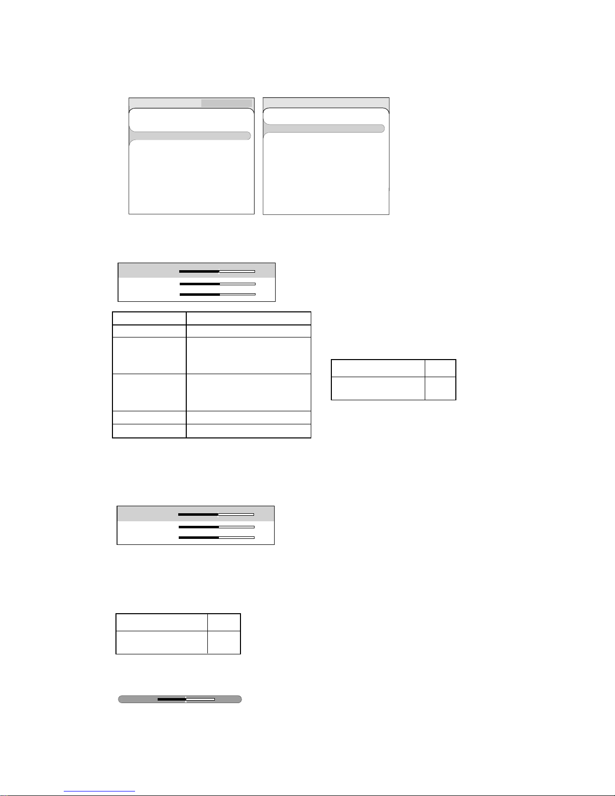
1 - ACCESING SERVICE MODE
EFC031E
1.1 TV set ON.
1.2 While keeping pressed the ”VOL-” key on the TV keyboard
press ”EXIT” on the RC until TV set switch on and enter service mode.
(Main menu).
IFC130 - EFC031E (according software version)
1.1 Switch the TV set into the Standby Mode.
1.2 While keeping pressed the ”VOL-” key on the TV keyboard press
”VOL-” on the RC until TV set switch on and enter service mode (Main menu).
2 - TEMPORARY EXIT FROM SERVICE MODE
2.1- 2.1- To temporary leave the Service Mode from the Main menu, goto the point ”Return”.
To access the everyday menus, press the ‘’Menu’’ button on the RCU.
Note :
- According to the type RCU it is possible to temporary leave the Service Mode by pressing Exit or Return key.
RETURN TO THE MAIN MENU
EFC031E
2.2 - To return to the Main menu, While keeping pressed the ”VOL-” key on the TV keyboard press
”Exit” on the RC until TV set switch on and enter service mode.
IFC130
2.2 - To return to the Main menu, press on the magenta key (”text”) on the RCU.
Note :
- A IFC130 menu not used during 3 minutes disappears. Press on the magenta key (”text”) on
the RCU to return to the Main menu.
3 - EXITING FROM SERVICE MODE
3.1- To exit the Service Mode switch off the mains supply to the TV.
All change in service mode will be saved in EEPROM automatically.
4 - EXITING FROM A SUB-MENU
4.1- To exit from a Sub-Menu (see §8) and return to the Main menu press the ”Exit key or the ”Return” key on the
RCU.
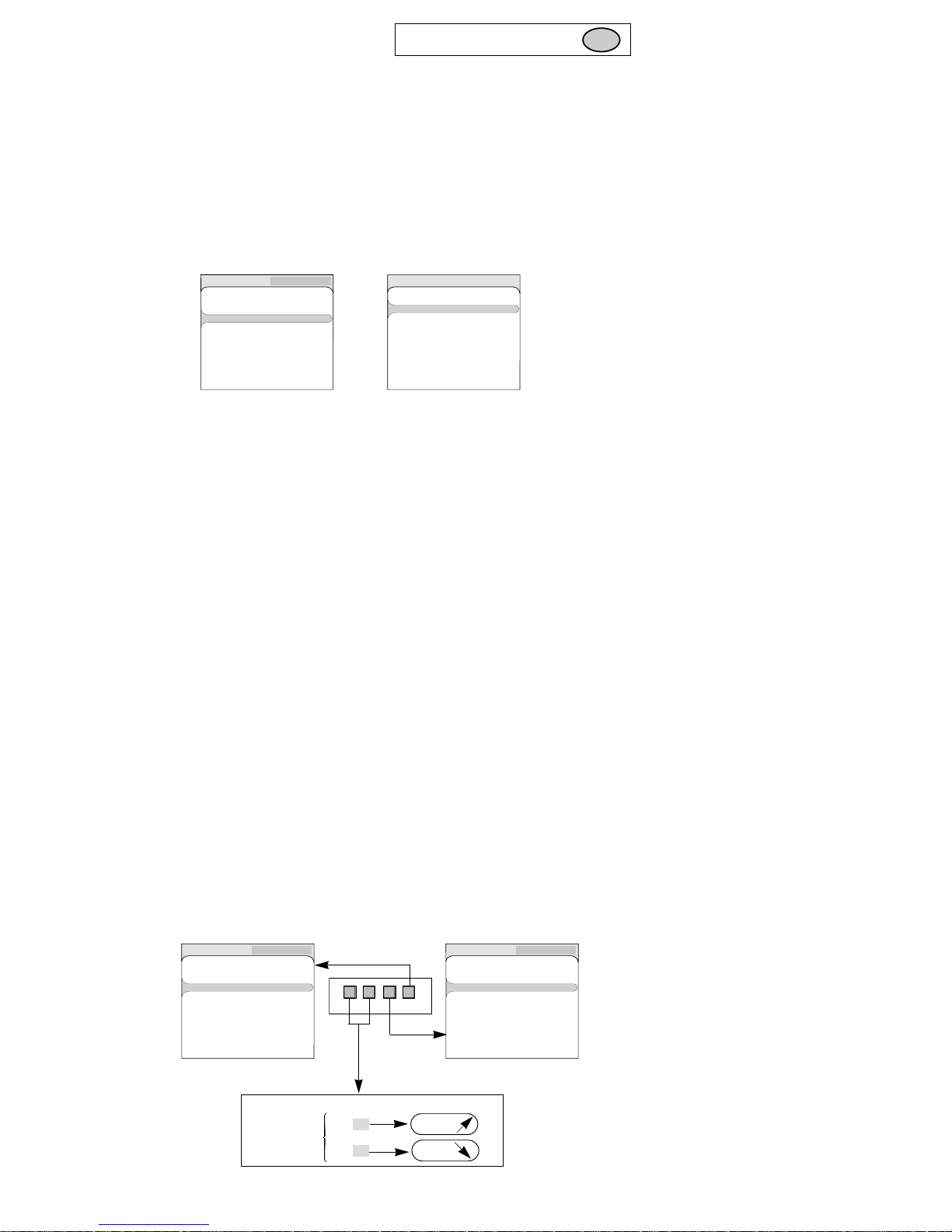
5 - NAVIGATION INSIDE THE SERVICE MODE
TV CONTROL PANEL
EFC031E - IFC130
First issue 02 / 06 1
I - SERVICE-MODE
EN
(
Factory setting
EFC031_X181-0
Return
Sound
Video
Field Service
...
...
...
...
Miscellaneous ...
EFC031E MAIN MENU
- Selec option*
- “Change value“
navigation up
Navigation down
VALUE
VALUE
Vol.
+
-
Vol.
PR
VOL
--
+
+
(
Factory setting
EFC031_X181-0
Return
Sound
Video
Field Service
...
...
...
...
Miscellaneous ...
(
Factory setting
EFC031_X181-0
Return
Sound
Video
Field Service
...
...
...
...
Miscellaneous ...
➠
➠
(
Service Menu
BL1.41
Return
Sound
Video
SAA7117AE
...
...
...
PW2300 ...
Misc ...
PW218 1st page ...
PW218 2nd page ...
IFC130 MAIN MENU
* Select option is possible with ”OK”
Page 3
REMOTE CONTROL
EFC031E - IFC130
2 First issue 02 / 06
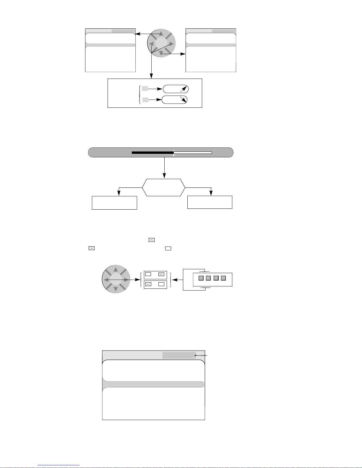
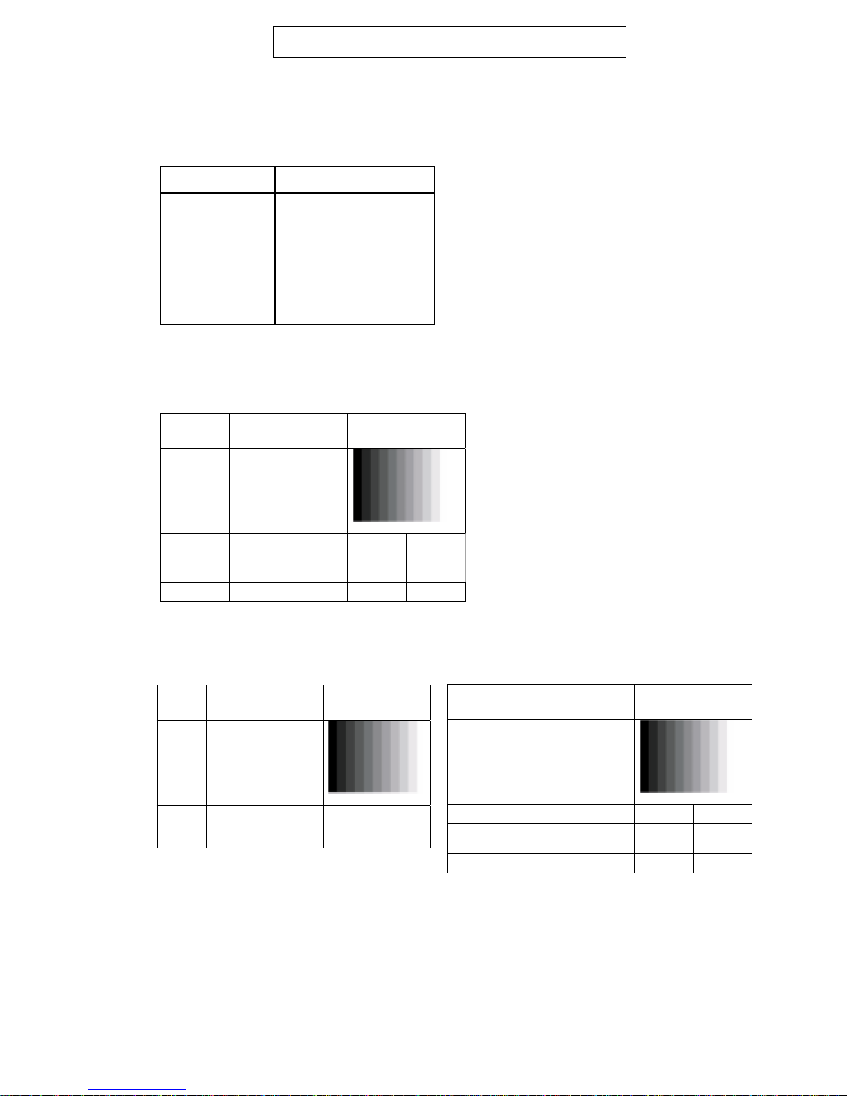
6 - DISPLAYING THE VALUE OF THE SETTING
VIDEO
7 - TOGGLE FUNCTION
To enable a function check (tick) the box.
: Implemented function : No implemented function
(Brightness -0003
Affichage
➠
+ >
NVM valeur
Affichage
➠
-
<
NVM valeur
Valeur décimale
Valeur de réglage
: NVM valeur
><
➠
➠
OK
PR
VOL
--
+
+
(
Factory setting
EFC031_X181-0
Return
Sound
Miscellaneous
Video
Field Service
...
...
...
...
...
Alignment
Alignement
Ableigh
Regolazione
Alineacion
Software version
Version Software
Software Version
Versione softaware
Versión software
- Select option*
- “Change“ value
(
Factory setting
EFC031_X181-0
Return
Sound
Video
Field Service
...
...
...
...
Miscellaneous ...
(
Factory setting
EFC031_X181-0
Return
Sound
Video
Field Service
...
...
...
...
Miscellaneous ...
➠
➠
Navigation up
Navigation down
OK
VALUE
VALUE
>
<
* Select option is possible with ”OK”
8 - LITE MENU FOR FIELD SERVICE
MAIN MENU
Page 4

EFC031E - IFC130
First issue 02 / 06 3
(
Factory setting
EFC031_X181-0
Return
Sound
Miscellaneous
Video
Field Service
...
...
...
...
...
Alignment
Alignement
Ableigh
Regolazione
Alineacion
Software version
Version Software
Software Version
Versione softaware
Versión software
SUBMENU
Page 5
EFC031E - IFC130
4 First issue 02 / 06
II - EFC031E CHASSIS - ALIGNMENT
1 VIDEO
1.1 Conditions
- The TV set should be warmed up for 60 minutes.
- The following conditions are automatically set when entering the Video submenu.
* Set these conditions in the User menu
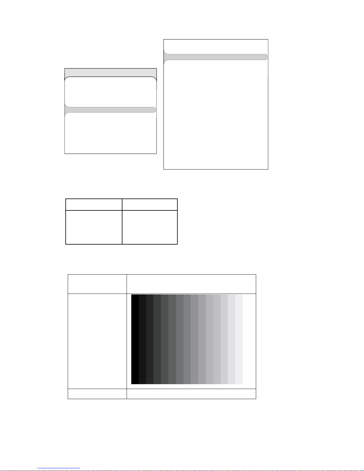
1.2 Y, Pb, Pr Component Input
Video test pattern
1.3 VGA Input
Standard Monitor Format (VESA) Standard TV Display Format
Test
Pattern
Philips test pattern 12 steps greyscale
Format 4:3 16:9 4:3 16:9
1H 576i25Hz 1080i25Hz576i25Hz 1080i25Hz
2H 576p50Hz 720p60Hz 576p50Hz 720p60Hz
Test
Pattern
Philips test pattern 12 steps greyscale
Picture
Format 4:3 16:9 4:3 16:9
1H 576i25Hz 1080i25Hz576i25Hz 1080i25Hz
2H 576p50Hz 720p60Hz 576p50Hz 720p60Hz
Test
Pattern
Philips test pattern 12 steps greyscale
Format
640x480@60Hz,
800x600@85Hz,
1280x1024@75Hz
640x480@60Hz,
800x600@85Hz,
1280x1024@75Hz
Function Alignment Value
Brightness Standard
Colour Standard
Contrast Standard (70%)
Black Extand Off...*
Tone Neutral...
Sharpness Not applicable*
Noise reduction Off...*
Couleur NTSC 50%
Mode zoom Standard
Page 6
EFC031E - IFC130
First issue 02 / 06 5
1.4
Video Calibration
EFC031E
1.4.1 MST9883 ADC Calibration
YPbPr Calibration for TV display format
- Connect Y, Pb, Pr signal to BV280 connector (”Video Components Enter”) with the following standard.
Input signal parameters:
- Exit temporary from Service Mode and select the ”Video Components Enter” (press the magenta key on the
RCU ”Text” to come back at the service mode )
- Video pattern to calibrate
- Select YPbPr and ”Calibration” in the ”Miscelaneous” Menu of Sevice Mode and press on
the RCU OK key .
The screen is flashing few minutes and stable after few seconds.
Signal Value (Vp-p)
Y: Sync to Peak white 0.7
Pr:Sync to Peak white 0.7
Pb:Sync to Peak white 0.7
Calibration Pattern
Color bar with no Gamma correction
Picture
Format 480p60Hz, 1H, 4:3
(
Factory Misc
(
Reset the values to ROM default Yes?
LUMA_TEMPORAL-NR
CHROMA_TEMPORAL-NR
Calibration ...
Debug ...
Reset the Alignment values
Yes?
TT 27Y24 Packet Enable*
Factory setting
EFC031_X181-0
Return
Sound
Video
Field Service
* According software version
...
...
...
...
Miscellaneous ...
Page 7

EFC031E - IFC130
6 First issue 02 / 06
1.4.2 RGB
RGB Calibration for Standard monitor format (VESA)
- Connect R, G, B Hsync and Vsync with following standard into VGA BV300
connector:
- Exit temporary from Service Mode and select the VGA enter (press the magenta key on the RCU ”Text” to come
back at the service mode)
- Video pattern to calibrate
- Select ”Calibration” in ”Miscelaneous” Menu of the Service Mode and press on the RCU ”OK” key.
The screen is flashing few minutes and stable after few seconds.
Note:
The others items of the ”Miscellaneous” menu are described at § 4.
Signal Value (Vp-p)
R (Red) 0.7
G (Green) 0.7
B (Blue) 0.7
Hsync. 2.4V
Vsync. 2.4V
Calibration Pattern
16 step Gray scale with no gamma
correction
Picture
Format 800x600@85Hz
Page 8
EFC031E - IFC130
First issue 02 / 06 7
2.1 Cut Off
Cutt Off alignment has to be done for the following standards :
Note: After Cut Off alignment control white point alignment. Repeat the adjustments if necessary.
R offset
G Offset
B Offset
+0007
+0024
+0016
- Insert a grey test pattern giving 15 Nits luminance level
- Measure the color co-ordinates near the screen center.
- Fix B Offset to the centre of the alignment range.
- Adjust R Offset - G Offset:
Colour Co-ordinates Value
x 0.282
y 0.293
Input Video Standard
SCART PAL / SECAM/ RGB
YPbPr SDTV (576i)
HDTV (108i 25)
HDTV (720p 60)
VGA VESA (DMT 1060)
SD Video (576i)
HD Video (1080i 25)
HDMI HDTV (720p 60)
FAV (CVBS) SD Video (576i)
(
Factory video
(Cut Off Alignment ...
Whitepoint alignment ...
Scalling Brightness Alignment ...
Scalling Color Alignment ...
Scale Tint Alignment ...
Peak White Alignment ...
Text Contrast alignment ...
Preset for Video Alignment ...
Factory setting
EFC031_X181-0
Return
Sound
Video
Field Service
...
...
...
...
Miscellaneous ...
EFC031E
2.2 Whitepoint
- Whitepoint alignment has to be done for the same standards of the Cuttoff alignment :
2.3 Scaling Brightness Alignment
- The Scalling Brightness is a factory alignment.
EFC031E: Brightness = +0003
R Gain
G Gain
B Gain
+0496
+0531
+0513
- Insert a grey test pattern with 50 IRE in one of the above mentioned standards.
- Measure the color co-ordinates near the screen center.
- Fix B Gain to the centre of the alignment range.
- Adjust R Gain - G gain to the following color co-ordinates:
Colour Co-ordinates Value
x 0.282
y 0.298
Brightness
-0003
2 - VIDEO ALIGNMENT
Page 9
EFC031E - IFC130
8 First issue 02 / 06
2.4 Scaling Colour
- Scaling Color Alignment has to be done for the following standards :
- 75% Color bar test pattern.
- Measure the Blue output and adjust Colour to equal levels as shown bellow:
2.5 Scale Tint
- No alignment for EU models.
2.6 Peak White Alignment
- Peak White test pattern (100%).Colourimeter.
- Peak White alignment has to be done for the following standards :
- Adjust Contrast to the level : 450 Nits +20% -15%.
2.7 Text Contrast.
- Selecting this item inserts a white centered pad.
- Measure the optical luminance output level (Y Nits) of the white pad.
- Adjust Text Contrast to the 60% of the PW level.
Colour
+0512
Input Video Standard
SCART PAL / SECAM/ RGB
YPbPr SDTV (576i)
HDTV (108i 25)
HDTV (720p 60)
VGA VESA (DMT 1060)
SD Video (576i)
HD Video (1080i 25)
HDMI HDTV (720p 60)
FAV (CVBS) SD Video (576i)
NTSC Tint
+0000
Contrast
+0534
Input Video Standard
SCART PAL / SECAM/ RGB
YPbPr SDTV (576i)
HDTV (108i 25)
HDTV (720p 60)
VGA VESA (DMT 1060)
SD Video (576i)
HD Video (1080i 25)
HDMI HDTV (720p 60)
FAV (CVBS) SD Video (576i)
Contrast
+0534
Text Contrast 14
Page 10
EFC031E - IFC130
First issue 02 / 06 9
3 - SOUND
- The items of the SOUND menu are not used
4 - MISCELLANEOUS
- EFC031E
4.1 Reset the values to ROM default
- Reset all the EEPROM data to FF.
Only required if the EEPROM data are corrupted.
After ”reset the values to ROM default” the alignment, calibration and channel installation is necessary.
4.2 LUMA_TEMPORAL_NR
- Temporal noise reduction setting for luminance.
Factory adjusted. It is not necessary to do adjustment on this item.
4.3 CHROMA_TEMPORAL_NR
- Temporal noise reduction setting for chrominance.
Factory adjusted. It is not necessary to do adjustment on this item.
4.4 Calibration
See § 1.4
4.5 Debug
- Bus quiet mode for main I2C Bus. Used only in development purpose.
4.6 Reset the Alignment values
- Reset all alignment values to default value. Used only if the TV need new alignment.
In that case it is necessary to start alignments by Video Calibration (ADC YPbPr).
Note:
After loading of a new software select ” Reset the alignment values” and check the TV alignment.
4.7 TT 27Y24 Packet Enable
According to software version. Factory adjust.
Improve teletext performance for some special French channels
(
Factory Misc
(
Reset the values to ROM default Yes?
LUMA_TEMPORAL-NR
CHROMA_TEMPORAL-NR
Calibration ...
Debug ...
Reset the Alignment values
Yes?
TT 27Y24 Packet Enable*
Factory setting
EFC031_X181-0
Return
Sound
Video
Field Service
* According software version
...
...
...
...
Miscellaneous ...
Page 11

EFC031E - IFC130
10 First issue 02 / 06
5 - FIELD SERVICE (Spécifique EFC031E)
5.1 Test Patterns
To check the Scaler Board:
- Press ”Left ” or ”Right ” key on RCU activate the purity test patterns in the following order:
Continous, white, black, red, green, blue, off.
5.2 Power Usage - LCD Usage
Power Usage and LCD Usage are time counters.
- ”Power Usage” indicates the Power supply number of service hours and minutes.
- ”LCD Usage” indicates the TV number of service hours and minutes.
The display is decimal.
5.3 Clear Event History
To clear all error codes stored in the NVM.
Action : Select the line and Press the right key on RCU to confirm.
5.4 Error Codes
1 - The last five Error codes are stored and displayed with a time stamp from the runtime counter.
Each each error code in this list has an error counter that counts further occurences of a particular error.
2 - If an error occurs that is already in the list the time stamp is updated and the error counter is
incremented anymore.
3 - The errors are displayed with the most recent error on top on the list. The others follow with descending
time stamps.
Displaying Error Codes with LED
1 - In addition to storing an error code it must also be displayed with TV’s standby LED.
Only the last error that occured is displayed.
2 - Decimal error codes from 11 to 18 are signaled.
3 - The error code is displayed as two separate digits separate by a suitable pause, this is repeated according
to a specific sequence.
For example Error-code 13 will be displayed thus :
1 flash and a short pause
3 flashes and a long pause
......
List of Error Codes
(Specific EFC031E):
11 ERR_EEPROM 15 ERR_TEA6415C
12 ERR_SAA7117A 16 ERR_MSP4411K
13 ERR_MST9883C 17 ERR_MAD4868
14 ERR_MASTER TUNER 18 ERR_TEA6422D
(
Factory setting
EFC031_X181-0
Return
Sound
Video
Field Service
...
...
...
...
Miscellaneous ...
Field Service
(Test patterns Off
Power Usage: 000030:29 LCD Usage: 000030:05
Clear Event History ...
Code Count Timestamp
00 000 000000:00
00 000 000000:00
00 000 000000:00
00 000 000000:00
00 000 000000:00
Page 12
EFC031E - IFC130
First issue 02 / 06 11
1 VIDEO
1.1 Conditions
- The TV set should be warmed up for 60 minutes.
- The following conditions are automatically set when entering the Video submenu.
* Set these conditions in the User menu
1.2 Y, Pb, Pr Component Input
Video test pattern
1.3 VGA I
Format Moniteur standard (VESA) Format affichage TV standard
Fonction Valeur
Lumière Standard
Couleur Standard
Contraste Standard (70%)
Noir renforcé Inactif*
Tonalité Neutre
Contour 50%
Réducteur de bruit Inactif*
Couleur NTSC 50%
Mode zoom Standard
Test
Pattern
Philips test pattern 12 steps greyscale
Format 4:3 16:9 4:3 16:9
1H 576i25Hz 1080i25Hz576i25Hz 1080i25Hz
2H 576p50Hz 720p60Hz 576p50Hz 720p60Hz
Test
Pattern
Philips test pattern 12 steps greyscale
Picture
Format 4:3 16:9 4:3 16:9
1H 576i25Hz 1080i25Hz576i25Hz 1080i25Hz
2H 576p50Hz 720p60Hz 576p50Hz 720p60Hz
Test
Pattern
Philips test pattern 12 steps greyscale
Format
640x480@60Hz,
800x600@85Hz,
1280x1024@75Hz
640x480@60Hz,
800x600@85Hz,
1280x1024@75Hz
III - IFC130 CHASSIS - ALIGNMENT
Page 13
EFC031E - IFC130
12 First issue 02 / 06
1.4
VIDEO CALIBRATION
1.4.1 YPbPr Calibration for TV display format
IFC130
- Connect Y, Pb, Pr signal to BV600 (”Video Components Enter”) with the following standard.
- Exit temporary from Service Mode and select the ”Video Components Enter” (press the magenta key on the
RCU ”Text” to come back at the service mode )
- Video pattern to calibrate
- Select ”YPbPr Calibration” in the ”PW218 1st page” Menu of the Service Mode and press the OK key on
the RCU.
The screen is flashing few minutes and stable after few seconds.
Signal Valeur (Vp-p)
Y: Sync to teak white 0.7
Pr:Sync to teak white 0.7
Pb:Sync to teak white 0.7
Calibration Pattern
Color bar with no Gamma correction
Picture
Format 720p60Hz, 2H, 16:9
(
Return
Panel Selection 009
Analog RGB Calibration
YCbCr Calibration
Factory Reset
BW Expand 000
CUEC / ICP 001
FRMEC 001
Flestone Correction 000
Film Mode 000
3:2 Film Sensitivity 000
2:2 Film sensitivity 004
Pixel Boost 000
DCS 000
DCTI 000
Peaking 001
Spatial noise Filter 000
LumaTemp.Noise Filter 064
LAI 000
Service Menu
BL1.41
Return
Sound
Video
SAA7117AE
...
...
...
PW2300 ...
Misc ...
PW218 1st page ...
PW218 2nd page ...
Page 14
EFC031E - IFC130
First issue 02 / 06 13
1.4 2 RGB
Analog RGB Calibration
- Connect R, G, B Hsync and Vsync with following standard into VGA BV300
connector:
- Exit temporary from Service Mode and select the VGA enter (press the magenta key on the RCU ”Text” to come
back at the service mode)
- Video pattern to calibrate
- Select ”Analog RGB Calibration” in the ”PW218 1st page” menu of the Service Mode and press the OK key on
the RCU.
The screen is flashing few minutes and stable after few seconds.
Note:
The others items of the ”PW218 1st page” are described at § 5.
Signal Value (Vp-p)
R (Red) 0.7
G (Green) 0.7
B (Blue) 0.7
Hsync. 2.4V
Vsync. 2.4V
Calibration Pattern
16 step Gray scale with no gamma
correction
Picture
Format 1024x768@60Hz
(
Return
Panel Selection 009
Analog RGB Calibration
YCbCr Calibration
Factory Reset
BW Expand 000
CUEC / ICP 001
FRMEC 001
Flestone Correction 000
Film Mode 000
3:2 Film Sensitivity 000
2:2 Film sensitivity 004
Pixel Boost 000
DCS 000
DCTI 000
Peaking 001
Spatial noise Filter 000
LumaTemp.Noise Filter 064
LAI 000
Service Menu
BL1.41
Return
Sound
Video
SAA7117AE
...
...
...
PW2300 ...
Misc ...
PW218 1st page ...
PW218 2nd page ...
Page 15
EFC031E- IFC130
14 First issue 02 / 06
2 - VIDEO ALIGNMENT
2.1 Cut Off
Cutt Off alignment has to be done for the following standards :
Note: After Cut Off alignment control white point alignment. Repeat the adjustments if necessary.
2.2 Whitepoint
-Whitepoint alignment has to be done for the same standards of the Cuttoff alignment :
2.3 Scaling Brightness Alignment
- Scaling Brightness Alignment est un réglage usine.
IFC130 : Brightness = +0024
- Insert a grey test pattern giving 15 Nits luminance level
- Measure the color co-ordinates near the screen center.
- Fix B Cutoff to the centre of the alignment range.
- Ajuster R Cutoff - G Cutoff:
Colour Co-ordinates Value
x 0.282
y 0.293
R Cutoff
G Cutoff
B Cutoff
-0028
-0004
-0016
Input Video Standard
SCART PAL / SECAM/ RGB
YPbPr SDTV (576i)
HDTV (108i 25)
HDTV (720p 60)
VGA VESA (DMT 1060)
SD Video (576i)
HD Video (1080i 25)
HDMI HDTV (720p 60)
FAV (CVBS) SD Video (576i)
IFC130
(
Service Video
(Cut Off Alignment ...
Whitepoint alignment ...
Scalling Brightness Alignment ...
Scalling Color Alignment ...
Scale Tint Alignment ...
Peak White Alignment ...
Text Contrast alignment ...
Preset for Video Alignment ...
Service Menu
BL1.41
Return
Sound
Video
SAA7117AE
...
...
...
PW2300 ...
Misc ...
PW218 1st page ...
PW218 2nd page ...
Coordonnées couleur Valeur
x 0.282
y 0.298
Brightness
-0003
R Gain
G Gain
B Gain
+0528
+0520
+0544
- Insert a grey test pattern with 50 IRE in one of the above mentioned standards.
- Measure the color co-ordinates near the screen center.
- Fix B Gain to the centre of the alignment range.
- Adjust R Gain - G gain to the following color co-ordinates:
Page 16
EFC031E - IFC130
First issue 02 / 06 15
2.4 Scaling Colour
- Scaling Color Alignment has to be done for the following standards :
- 75% Color bar test pattern.
- Measure the Blue output and adjust Colour to equal levels as shown bellow:
2.5 Scale Tint
-
No alignment for EU models.
2.6 Peak White Alignment
- Peak White test pattern (100%).Colourimeter.
- Peak White alignment has to be done for the following standards :
- Adjust Contrast to the level : 450 Nits +20% -15%.
3 - SOUND
- The items of the SOUND menu are not used.
4 - MISCELLANEOUS
- IFC130
Colour
+0512
NTSC Tint
+0000
Contrast
+0534
Input Video Standard
SCART PAL / SECAM/ RGB
YPbPr SDTV (576i)
HDTV (108i 25)
HDTV (720p 60)
VGA VESA (DMT 1060)
SD Video (576i)
HD Video (1080i 25)
HDMI HDTV (720p 60)
FAV (CVBS) SD Video (576i)
Input Video Standard
SCART PAL / SECAM/ RGB
YPbPr SDTV (576i)
HDTV (108i 25)
HDTV (720p 60)
VGA VESA (DMT 1060)
SD Video (576i)
HD Video (1080i 25)
HDMI HDTV (720p 60)
FAV (CVBS) SD Video (576i)
(
Misc
Return
ADC Calibration ...
Test pattern ...
Service Menu
BL1.41
Return
Sound
Video
SAA7117AE
...
...
...
PW2300 ...
Misc ...
PW218 1st page ...
PW218 2nd page ...
Page 17
EFC031E - IFC130
16 First issue 02 / 06
4.1 ADC Calibration
- Not used in this Menu.
The ADC Calibration adjustment is done in the ”PW218 1st page” (see § 1.4).
4.2 Test pattern
To check the Scaler Board:
- Press ”Left ” or ”Right ” key on RCU activate the purity test patterns in the following order:
Continous, white, black, red, green, blue, off.
5 -PW218 1st page - PW218 2nd page - PW2300 (spécific IFC130)
NOTE :
The Analog RGB Calibration and YCbCr Calibration items are described at §1.4.
Except other indication the following items , only deal with factory adjustments. Their
meaning is given for information only.
5.1 - PW218 1st page
Panel Selection
- Different panel timing selection.
Factory adjust.
If this item is modified, set it to the previous value (009) then exit from the Service Mode and enter again.
(
Return
Panel Selection 009
Analog RGB Calibration
YCbCr Calibration
Factory Reset
BW Expand 000
CUEC / ICP 001
FRMEC 001
Flestone Correction 000
Film Mode 000
3:2 Film Sensitivity 000
2:2 Film sensitivity 004
Pixel Boost 000
DCS 000
DCTI 000
Peaking 001
Spatial noise Filter 000
LumaTemp.Noise Filter 064
LAI 000
Service Menu
BL1.41
Return
Sound
Video
SAA7117AE
...
...
...
PW2300 ...
Misc ...
PW218 1st page ...
PW218 2nd page ...
!
Page 18

EFC031E - IFC130
First issue 02 / 06 17
Factory Reset
- Factory reset of EEPROM data to default value.
Used only if the alignment have somthing wrong and need to align the TV again.
Installed channel will lost. ADC calibration no change.
Note:
After loading of a new software select ” Factory reset” and check the TV alignment.
BW Expand: Black expand.
CUEC/ICP: Color Upsampling Error Correction / Inter-Chroma Processing.
FRMEC: Frame Rate Motion Error Correction.
Fleshtone Correction: Color correction.
Film Mode: Film Mode On / Off.
3:2 Film Sensitivity - 2:2 Film Sensitivity: Film Mode 3:2 (or 2:2) sensitivity setting.
Pixel/Boost : Pixel boost On / Off.
DCS: Dynamic Color Saturation.
DCTI: Digital Color Transient Improvement
Peaking: Peaking Gain setting.
Spatial Noise Filter: Spatial Noise Filtering setting.
LumaTemp Noise Filter: Luma temporal Noise filtering setting.
LAI : Low Angle Interpolation
5.2 - PW218 2nd page
Blue Cal: Blue Calibration.
BWE Enable: Black White Expansion On / Off.
BWE Mode : Black White Expansion Mode.
DYNKDEINT Enable: Dynamic Motion weighting factor for DEINTerlacer
5.3 SAA7117AE
Not used.
(
Quit
Blue Cal 000
BWE Enable 000
BWE Mode 000
DYNKDEINT Enable 001
Service Menu
BL1.41
Return
Sound
Video
SAA7117AE
...
...
...
PW2300 ...
Misc ...
PW218 1st page ...
PW218 2nd page ...
Page 19

EFC031E - IFC130
18 First issue 02 / 06
5.4 PW2300
Selected Feta: Select the PW2300 IC if there are>1.
3D Comb Filter: Validation On / Off de 3D Comb Filter.
FTC Level: Fleshtone correction Level.
FTC Angle: Fleshtone correction Angle.
DCTI Gain: Digital Color Transient Improvement Gain.
DCTI frequency: Digital Color Transient Improvement Frequency.
Luma Peaking Gain: Luma Peaking gain.
Luma Peaking L Threash: Luma Peaking Lower Threshold.
Luma Peaking U Threash: Luma Peaking Upper Threshold.
Luma Peaking L Trans: Luma Peaking Lower Transient.
Luma Peaking U Trans: Luma Peaking Upper Transient.
Luma Sharpness gain: Luma Sharpness Gain.
Luma Sharpness freq: Luma Sharpness Filter Cutoff frequency.
Black Stretch: Black Strech On / Off.
White Stretch: White Strech On / Off..
(
Selected Feta 000
3D Comb Filter 001
FTC Level 128
FTC Angle 035
DCTI Gain 007
DCTI Frequency 000
DLTI Gain 000
DLTI Frequency 000
Luma Peaking Gain 000
Luma Peaking L Threash 001
Luma Peaking U Threash 000
Luma Peaking L Trans 000
Luma Peaking U Trans 000
Luma Sharpness Gain 000
Luma Sharpness Freq 003
Black Stretch 128
White Stretch 128
Service Menu
BL1.41
Return
Sound
Video
SAA7117AE
...
...
...
PW2300 ...
Misc ...
PW218 1st page ...
PW218 2nd page ...
Page 20
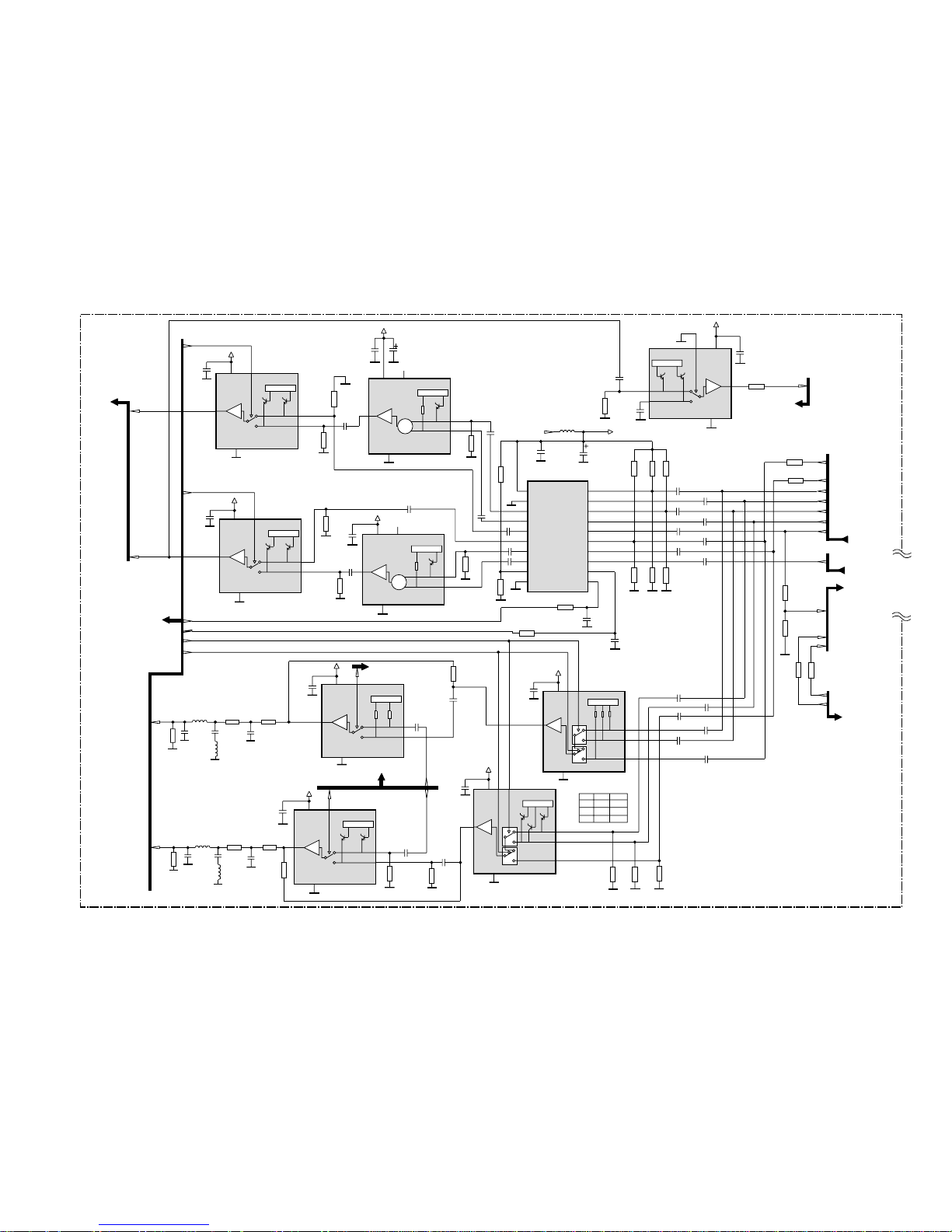
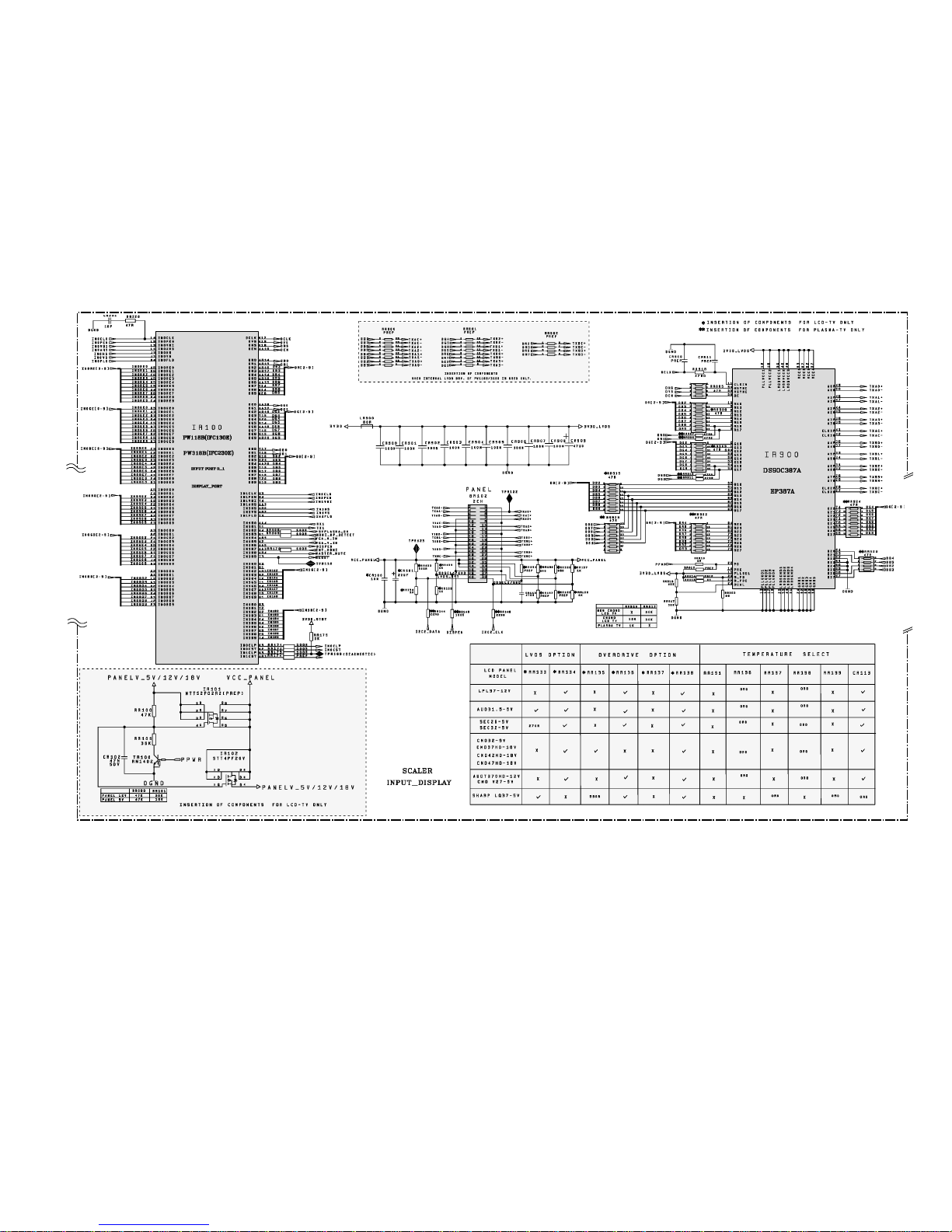
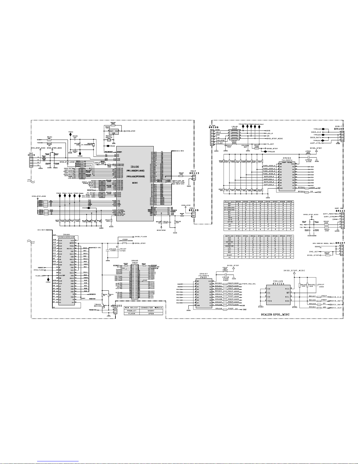
EFC031-IFC130-IFC230
First issue 12/05
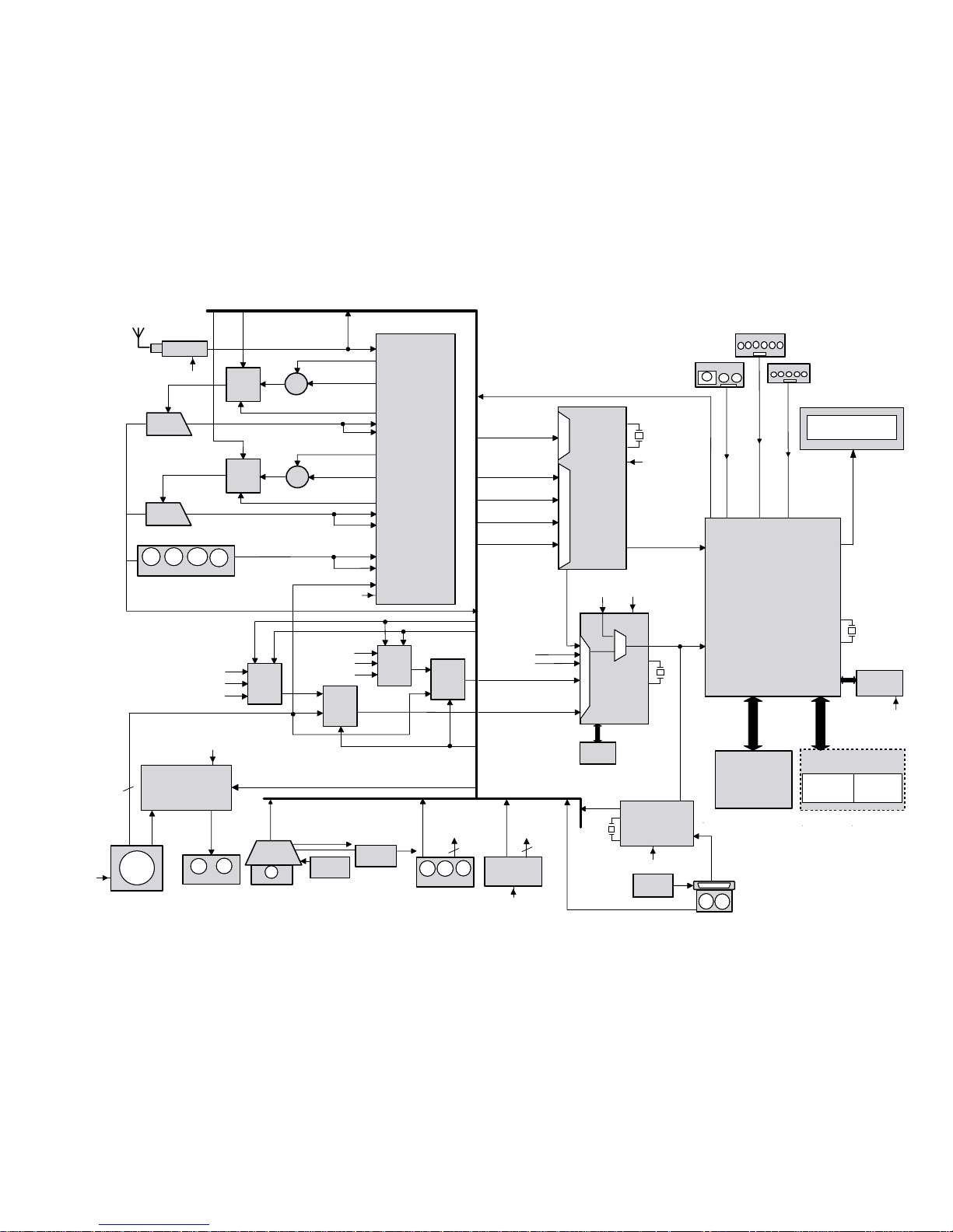
IFC130E I/O Concept
Flash Memory
32Mbit
M29W320EB70N6
CH1
32bits data
12bits address
16bits data
21bits address
5 channel
LVDS
signal
CH0
64kbit
EEPROM
14.318
MHz
Scart 1
Scart 2
MA_Tuner
+
MM 1507
MM 1511
MM 1511
Mux/ Drv
MM 1507
Mux/ Drv
+
HALF
SCART
FULL
SCART
cv
cv
TEA6415C
CHR
Y
Y
AV1_CVBS_OUT
AV1_Y_OUT
AV1_CHR_IN
CHR
AV1_CHR_OUT
AV1_CVBS/Y_IN
INTERBOARD
CONNECTION
MA_TUNER_CVBS
AV2_Y_OUT
AV2_CHR_OUT
AV2_CVBS_OUT
AV2_CVBS/Y_IN
AV2_CHR_IN
CVBS_OUT
CVBS_OUT
FAV_CVBS/Y_IN
FAV_CHR_IN
Flat Panel Display
MA_Tuner
_CVBS
'L'=YC
'H'=CVBS
'L'=YC
'H'=CVBS
19
19
TV K B
DVD KB
FRONT CINCH
CVBS SVHS
LVDS OUT
IR
0x40/
0x48H
CVBS_3D
MA_Tuner_CVBS
32.11
MHz
MUX MUX
AV1_CVBS/YC
Scart1
AV2_CVBS/YC
Scart2
FAV_CVBS/YC
FAV
RGB+FB
Scart1
24-bits RGB
H+V+Clock
16MB
SDRAM
VGA_RGB
27
MHz
MU X
MUX
DDR Frame Buffer
4Mx32bitsx4banks
MT46V16M16-6T
256Mbit
(166MHz)
MT46V16M16-6T
256Mbi
(166MHz)
C_AV_IN
YC_SEL_CTRL1
Audio Block
Diagram
VGA_TX, VGA_RX
VGA_Right_Audio
VGA_Left_Audi0
MM1117/
1117/
MM1228
MM1113/
MM1224
C Mux
C_AV1
C_AV2
AV3/FAV_CHR_IN
Y_AV1
Y_AV2
AV3/FAV_CVBS/Y_IN
VGA_RGB
RS232
DRV
VGA
2kbit
EEPROM
COMP_YPbPr1
DVD
Y_AV_IN
YC_SEL_CTRL2
DVD_Right_Audio
DVD_Left_Audio
Master_Mute
Audio_STBY
RESET_AUDIO
YC_SEL_CTRL1
YC_SEL_CTRL2
CVBSOUT_AV1_CTRL
CVBSOUT_AV2_CTRL
YC_DVD_SEL_CTRL
Video
Decoder
PW2300
Video
Decoder
SAA7117A
LCD/Plasma TV
Controller
PW118B
COMP_YPbPr2
Card Reader
Module
FE6233
MM1508
Y Mux
Y Mux
MM1506
C Mux
YC_DVD_SEL_CTRL
Comp IN
UART1
DVD_CVBS
DVD_YC
DVD_CVBS
Audio Jack
H-port 8 bits
I-port 8 bits
H+V+Clock
16-bits YCbCr
H+V+Clock
LINE_O/P_L
LINE_O/P_R
Audio Cinch Output
UART1
COMP_YPbPr2
COMP_YPbPr1
Prepared
2kbit
EEPROM
TMDS
28.322
MHz
HDMI Rx
SiI9011
LRCLK, BCLK,
PCMDATA
HDMI_Right_Audio
HDMI_Left_Audio
CVBSOUT_AV2_CTRL CVBSOUT_AV1_CTRL
0xC2H
I2 C
0x06H
I2 C
0xA0H
I2 C
I
2
CC 0x80, 82, 9AH
VGA_Right_Audio, VGA_Left_Audio
Comp_Right_Audio, Comp_Left_Audio
Comp_Right_Audio
Comp_Left_Audio
Card Reader_Right_Audio, Card Reader_Left_Audio
Card Reader_Right_Audio
Card Reader_Left_Audio
Master_Mute
AUDIO_STBY
RESET_AUDIO
RGB+FB Scart1, AV1_CVBS/YC Scart1
FAV_CVBS/YC FAV
AV2_CVBS/YC Scart2
0x06H
I2 C
0xA0H
I2 C
0x66H
I2 C
0xA0H
I2 C
I
2
C
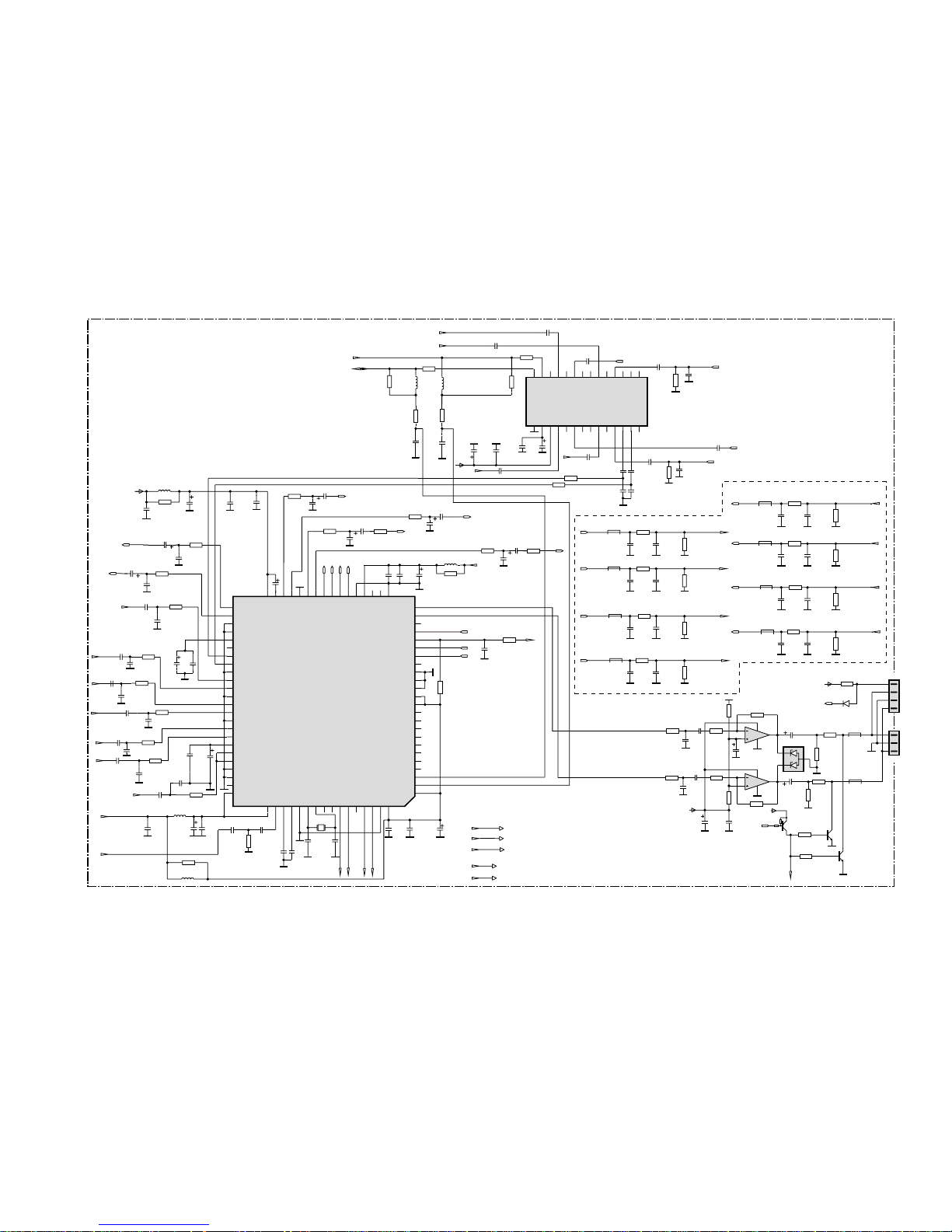
BLOCK DIAGRAM - SCHEMA SYNOPTIQUE - BLOCKSCHALTBILD - SCHEMA A BLOCCHI - ESQUEMA DE BLOQUES
Page 21
EFC031-IFC130-IFC230
First issue 12 / 05
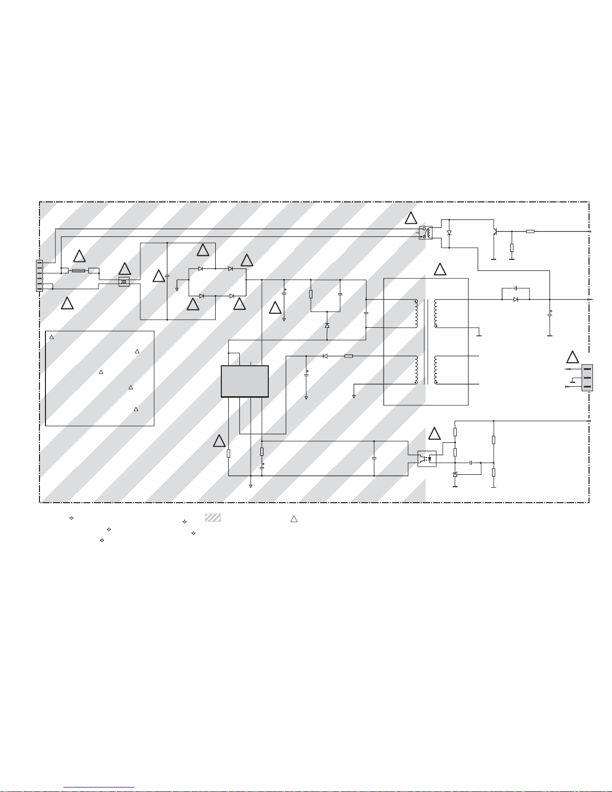
Note :
Power Supply primary circuit measurements.
- Use only ( ) connection point.
Attention :
Mesure dans la partie primaire de l'alimentation
- Utiliser la masse du bloc alimentation ( ).
Achtung :
Bei Messungen im Primärnetzteil
- Primärnetzteilmasse verwenden ( ).
Attenzione :
misure nell'alimentatore primario
- usare massa alimentazione primario ( ).
Cuidado :
Medida en el bloque de alimentacion
- Utilizar la masa del bloque de alimentacion ( ).
Part of board connected to mains supply.
Partie du châssis reliée au secteur.
Primärseite des Netzteils.
Parte dello telaio collegata alla rete.
Parte del chasis conectada a la red.
Use isolating mains transformer
Utiliser un transformateur isolateur du secteur
Einen Trenntrafo verwenden
Utilizzare un transformatore per isolarvi dalla rete
Utilizar un transformador aislador de red
!
Indicates critical safety components, and identical components should be used
for replacement. Only then can the operational safety be garanteed.
Le remplacement des éléments de sécurité (repérés avec le symbole ) par
des composants non homologués selon la Norme CEI 65 entraine la non-conformité
de l'appareil. Dans ce cas, la responsabilité dufabricant n'est plus engagée.
!
!
!
!
Wenn Sicherheitsteile (mit dem Symbol gekennzeichnet) durch nicht
normgerechte Teile ersetzt werden, erlischt die Haftung des Herstellers.
La sostituzione degli elementi di sicurezza (marcati con il segno ) con
componenenti non omologati secondo la norma CEI 65 comporta la non conformitá
dell'apparecchio. In tal caso é “esclusa la responsabilità” del costruttore.
La subtitución de elementos de seguridad (marcados con el simbolo ) por
componentes no homologados segun la norma CEI 65, provoca la no
conformidad del aparato. En ese caso, el fabricante cesa de ser responsable.
!
TL431
VAL?
FB
D
D
Vcc
OCP
GND
startup
T500mAL 250V
FP610
CP611
22U
400V
RP612
1R2/2W
DP612
FS1MI
DP613
FS1MI
CP612
1N
1KV
34
562178
STR-A6159
IP610
CP602
220N
1
4
3
2
LP600
1
2
3
4
5
6
BP600
RP611
150K
RP616
1K
FP610A
FP610B
H
DP601
1N4148W
DP614
FS1MI
DP611
FS1MI
CP617
820P
DP616
SR560
CP616
470U
1
2
4
5
10
9
8
7
SMT_STBY8
LP610
CP610
220P
5VSTBY
RP613
62R
RP601
3K3BC848B
TP601
3
2
1
BP610
DP615
FUF4005
GND
5VSTBY
RP618
2K
RP617
2K43
RP615
220R
RP614
10K
RP602
22K
1
2
3
4
IP630
TCET1103G
IP620
DP617
RGP15G
CP618
100N
CP615
680P
CP614
10U
CP613
22U
50V
GNDGND
GND
GND
H
H
PO
5VSTBY
GND
PO
GND
H
4
5
1
2
3
SP600
AC5
AC3
AC4
H
!
!
!
!
!
!
!
!
!
!
!
!
!
!
POWER SUPPLY - ALIMENTATION - NETZTEIL - ALIMENTAZIONE - ALIMENTACIÓN
SCHEMATIC DIAGRAM - SCHEMA DE PRINCIPE - SCHALTBILD - SCHEMA - ESQUEMA
Page 22
EFC031-IFC130-IFC230
First issue 12/05
9
8
10
11
13
12
14
15
16
17
18
19
20
21
7
5
1
2
3
4
6
1
2
9
8
10
11
13
12
14
15
16
17
18
19
20
21
7
5
1
2
3
4
6
1
2
NSAD500H
*
R_OUT_AV2
L_OUT_AV2
CVBS_OUT
AV1
R_OUT_AV1
R_IN_AV1
L_OUT_AV1
AUDIO-GND
BLUE-GND
L_IN_AV1
CVBS_OUT
CVBS_IN
RGB-GND
SHIELD-GND
RED-GND
SPARE
Green
DATA
GREEN-GND
Blue
SHIELD-GND
CVBS_IN
RGB-GND
RED-GND
GREEN-GND
BLUE-GND
AUDIO-GND
SBLK
Red/Chroma
FBLK
AV2
DIGITAL INTERFACE
AUDIO
L_IN_AV2
R_IN_AV2
DIGITAL INTERFACE
SYNC/CVBS-GND
SYNC/CVBS-GND
CHROMA
AUDIO
FRONT AV
SBLK
AUDIO
*
*
*
*
NOT INSERTED
VIDEO SWITCHING
POWER INTERFACE
VIDEO SWITCHING
AUDIO
DIGITAL INTERFACE
RF Module
VIDEO SWITCHING
DIGITAL INTERFACE
SYNC/CVBS-GND
SYNC/CVBS-GND
TECI
AUDIO VIDEO INPUT (AV IN)
DIGITAL INTERFACE
SCH IFC130E AV BOARD
SW_AV1_CVBS/Y_IN
I2C0/1_DA
I2C0/1_CL
I2C0/1_CLK
I2C0/1_DATA
I2C0_DATA
I2C0_CLK
I2C0_DA
I2C0_CL
DE101
12345678910
BE100
1234
8765
RE101
68R
AGND
AGND
75R
RX110
ZMM6.8
DX206
8K2 1%
RX114
1K 1%
RX122
ZMM6.8
DX103
ZMM6.8
DX105
75R
RX115
CX100
18P0
18P
CX126
CX101
18P
100R
RX212
18P
CX131
CX201
18P0
100R
RX210
100R
RX113
27R
RX100
47R
RX101
ZMM15
DX106
18P0
CX202
18P
CX130
18P
CX218
18P
CX219
18P
CX125
75R
RX211
18P
CX217
1
10
11
12
13
14
15
2
3
4
5
6
7
8
9
BH101
BX101
RX501
47R
RX213
1K 1%
CX200
18P0
DX200
ZMM15
BX200
LX105
27R
RX504
47R
RX503
27R
RX500
27R
RX112
100R
RX108
47R
LX107
120Z
DX100
ZMM6.8
100R
RX131
CX129
18P
DX101
ZMM6.8
27R
RX104
RX102
27R
RX103
47R
CX127
18P
LX106
120Z
47R
RX105
DX102
ZMM6.8
22P
CX509
LX503
120Z
1
2
3
4
5
6
7
8
9
BX500
RX505
237R
1%
JX200
0R
JX100
0R
CX128
18P
RX130
47R
CX102
18P
RX107
27R
LX506
3U3
1%
237R
RX506
22P
CX508
RX202
47R
RX201
27R
LX500
120Z
22P
CX500
LX504
3U3
1%
237R
RX502
LX502
120Z
LX501
120Z
RX208
27R
LX103
120Z
ZMM6.8
DX202
LX207
120Z
LX100
120Z
DX104
ZMM6.8
LX104
120Z
RX209
47R
LX204
120Z
LX101
120Z
LX505
3U3
22P
CX501
RX507
237R
1%
LX507
3U3
ZMM6.8
DX201
LX206
120Z
18P0
CX213
RX200
8K2 1%
LX201
120Z
AGND
SW_AV2_CHR
AGND
AV1_RED/C_IN
AGND
AGND
AGND
AGND
AGND
AGND
AGND
CVBS_AV1_OUT
SW_AV2_CVBS/Y_IN
AGND
AGND
AGND
AGND
AGND
AGND
AGND
SW_AV1_R/CHR
AV1_PIN8_IN
AGND
AV1_PIN16
CVBS_AV2_OUT1
AGND
+6V5
AM_AF
CVBS_IFM
SIF
I2C0_DATA
I2C0_CLK
AV1_BLUE
AV2_PIN8_IN
AGND
AGND
AGND
R_OUT_AV2
AGND
FCB_L_IN
AV1_GREEN
AV2_CVBS/Y_IN
AGND
AGND
AGND
AGND
AGND
FCB_R_IN
AGND
AV1_CVBS/Y_IN
L_IN_AV1
F_CHROMA_IN
AGND
FCB_CHROMA_IN_LOW
AGND
AGND
AGND
AGND
FCB_CVBS/Y_IN_LOW
AGND
AGND
AGND
AGND
AGND
FCB_CHROMA_IN
FCB_CVBS/Y_IN
AGND
AGND
SW_F_CHROMA_IN
SW_F_CVBS/Y_IN
AGND
R_OUT_AV1
R_IN_AV1
L_OUT_AV1
AGND
AGND
AGND
F_CVBS/Y_IN
AGND
AGND
GND
AGND
AGND
AGND
AGND
L_IN_AV2
GND
AGND
R_IN_AV2
AGND
AV2_C_IN
L_OUT_AV2
AGND
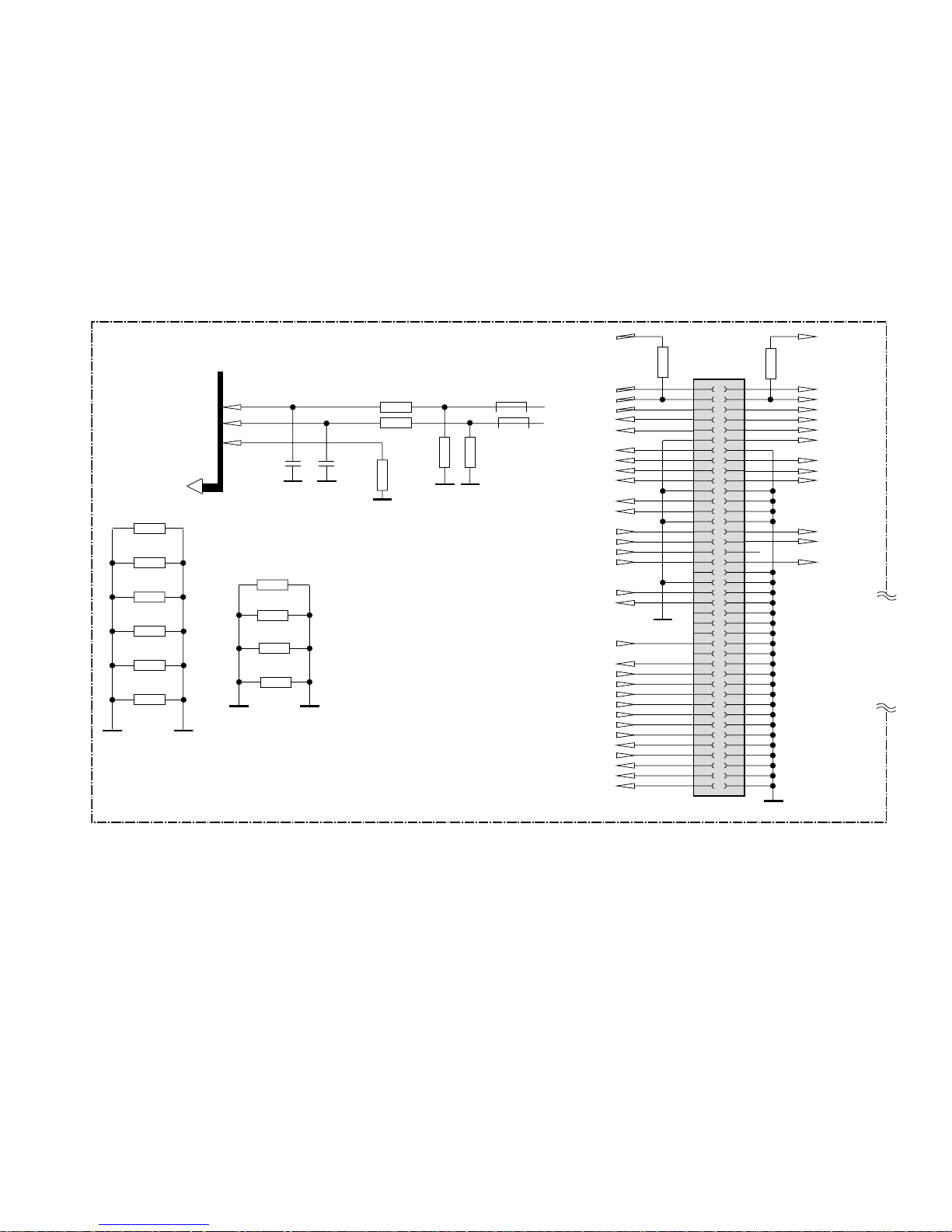
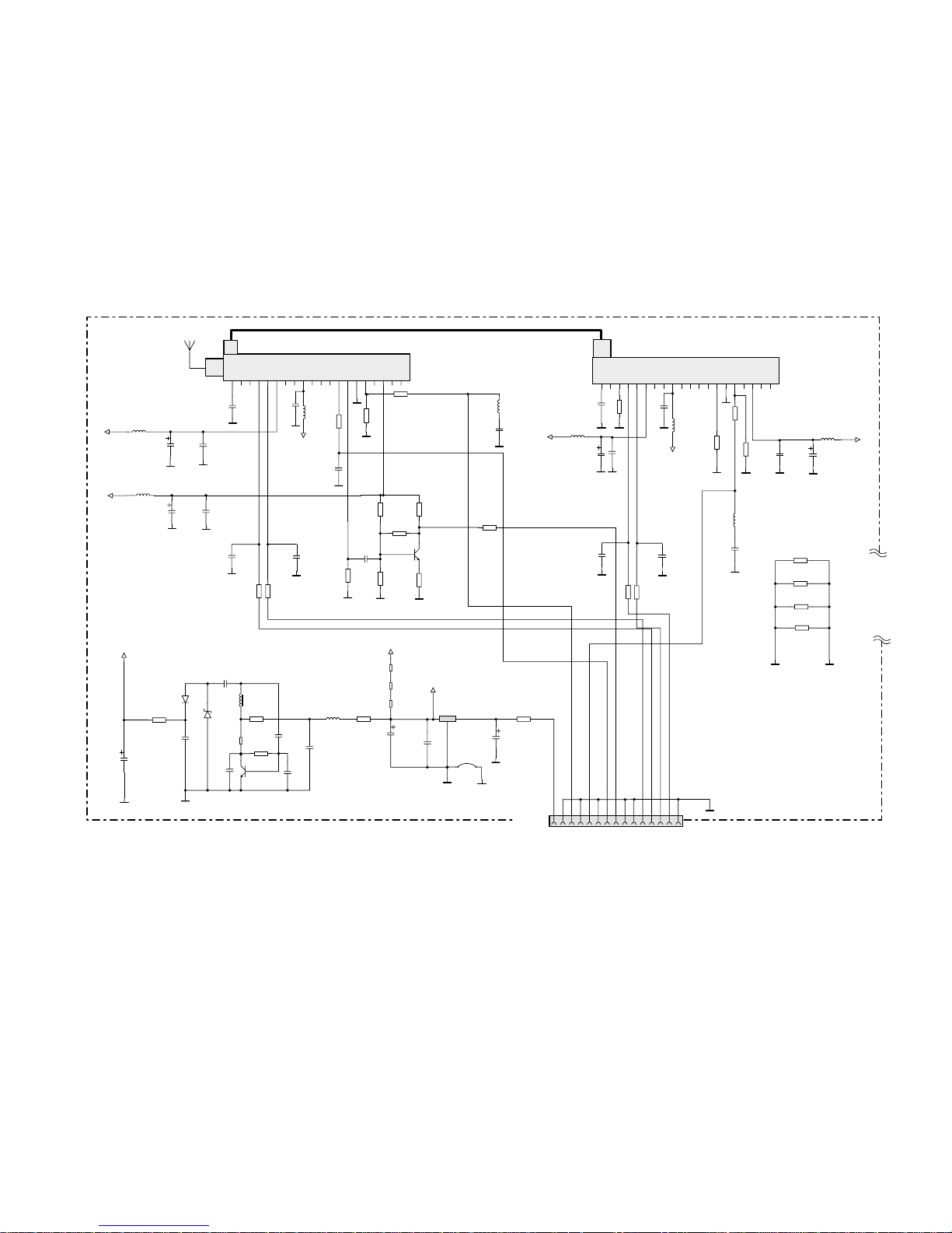
MAIN SCHEMATIC DIAGRAM - SCHEMA DE LA PLATINE PRINCIPALE - SCHALTBILD HAUPTPLATINE - SCHEMA DELLA PIASTRA PRINCIPALE- ESQUEMA DE LA PLATINA PRINCIPAL
Page 23
EFC031-IFC130-IFC230
First issue 08 / 04
8
GND
6
VCC
3
IN2
2
SW1
1
IN1
5
IN3
SW2
4
7
OUT
CLAMP
BIAS
BUF
CLAMP
CLAMP
8
GND
1
IN1
7
OUT
6
VCC
3
IN2
2
SW1
5
IN3
SW2
4
15K
15K
BUF
15K
BIAS
GND
IN1
IN2
OUT
SWVCC
MM1506
BIAS
15k 15k
DRV.
6dB
GND
IN1
IN2
OUT
SWVCC
MM1508
BIAS
CLAMPCLAMP
DRV.
6dB
MM1511
5
GND
6
YIN
4
CIN
2
OUT
1NC3
VCC
BIAS
CLAMP
15k
+
6dB
-6dB
5
GND
6
IN1
4
IN2
2
OUT
1SW3
VCC
MM1507
BIAS
CLAMPCLAMP
DRV.
MM1511
5
GND
6
YIN
4
CIN
2
OUT
1NC3
VCC
BIAS
CLAMP
15k
+
6dB
-6dB
5
GND
6
IN1
4
IN2
2
OUT
1SW3
VCC
MM1507
BIAS
CLAMPCLAMP
DRV.
5
GND
6
IN1
4
IN2
2
OUT
1SW3
VCC
MM1507
BIAS
CLAMP CLAMP
DRV.
1
IN1
3
IN2
5
IN3
6
IN4
8
IN5
10
IN6
11
IN7
20
IN8
2
DATA
4
CLOCK
9
VCC
7
PROG
19
GND2
12
GND1
OUT6
18
17
OUT5
OUT4
16
15
OUT3
OUT2
14
13
OUT1
DIGITAL INTERFACE
H
L
DIGITAL INTERFACE
H
L
DIGITAL INTERFACE
L
H
L
L
AV IN
VIDEO SWITCHING
AV IN
DIGITAL INTERFACE
H
H
L
OUTSW2SW1
LL
H
H-- IN3
IN2
IN1
AV IN
Truth Table
DIGITAL INTERFACE
DIGITAL INTERFACE
MM1113/MM1117
SCH IFC130E AV BOARD
CX600
100N
TEA6415C
IX802
AV3/F_CVBS_IN
AV3/F_CHROMA_IN
F_CVBS/Y_IN
MA_TUNER_CVBS
SW_AV1_R/CHR
SW_F_CHROMA_IN
JX800
0R
YC_SEL_CTRL1
SW_F_CVBS/Y_IN
CX814
100N
10VA
CVBS_AV2_OUT2
CX836
100N
CX827
100N
AGND
AGND
RX859
PREP
RX858
0R
JX801
0R
RX120
100K
CX826
1U
AGND
RX856
100R
I2C0/1_CLK
CX834
33P
CX835
33P
I2C0/1_DATA
AGND
CX809
1UF
AGND
RX846
100K
RX845
100K
CVBS_AV1_OUT
CX815
1U
CVBSOUT_AV2_CTRL
CVBSOUT_AV1_CTRL
CX807
1UF
CX810
1UF
CX806
1UF
CX800
1UF
CX650
1UF
CX104
1UF
CX204
1UF
CX801
1UF
CX105
1UF
CX205
1UF
CX824
100N
YC_SEL_CTRL2
CX825
100N
10VA
10VA
10VA
10VA
CX804
100N
CX802
22N
10VA
10VA
CVBS_AV2_OUT1
RX841
100K
CX812
1UF
RX847
100K
RX844
100K
AGND
AGND
AGND
RX843
100K
CX106
22N
AGND
AGND
RX811
75R
SW_AV2_CHR
AGND
AGND
AGND
F_CHROMA_IN
JX803
0R
JX802
0R
CX811
100N
CX206
22N
CX203
22N
SW_AV2_CVBS/Y_IN
AGND
10V
RX121
100K
AGND
AGND
AGND
AGND
AGND
AGND
AGND
AGND
AGND
AGND
AGND
AGND
AGND
AGND
AGND
22N
CX103
CX803
47UF
CX124
22N
CX808
100N
CX816
100N
RX116
100K
RX118
100K
CX813
100N
CX805
100N
RX650
27R
RX651
47R
RX117
100K
RX119
100K
LX800
10UH
CX820
47UF
AGND
RX849
100K
AGND
AGND
RX848
100K
AGND
RX840
100K
AGND
AGND
RX842
100K
AGND
AGND
RX857
100R
10VA
AGND
IX809
IX804
IX803
IX806
IX805
CVBS_IFM
SW_AV1_CVBS/Y_IN
5
6
4
2
13
IX810
100N
CX829
RX853
34R8
0R
JX804
100K
RX839
1UF
CX832
1UF
CX833
100K
RX838
75R
RX854
40R2
RX855
47P
CX854
LX853
10NH
CX855
270P
CX853
470P
560NH
LX852
100N
CX831
0R
JX805
5
6
4
2
13
IX811
RX850
34R8
75R
RX851
CX830
100N
CX850
470P
40R2
RX852
47P
CX851
LX851
10NH
CX852
270P
560NH
LX850
CX828
100N
YC_DVD_SEL_CTRL
AGND
D_Y
AGND
Y_AV_IN
AGND
AGND
AGND
AGND
AGND
AGND
D_CHR
YC_DVD_SEL_CTRL
AGND
C_AV_IN
AGND
AGND
AGND
AGND
AGND
10VA
10VA
MM1113
IX807
MM1117
IX808
D_CVBS
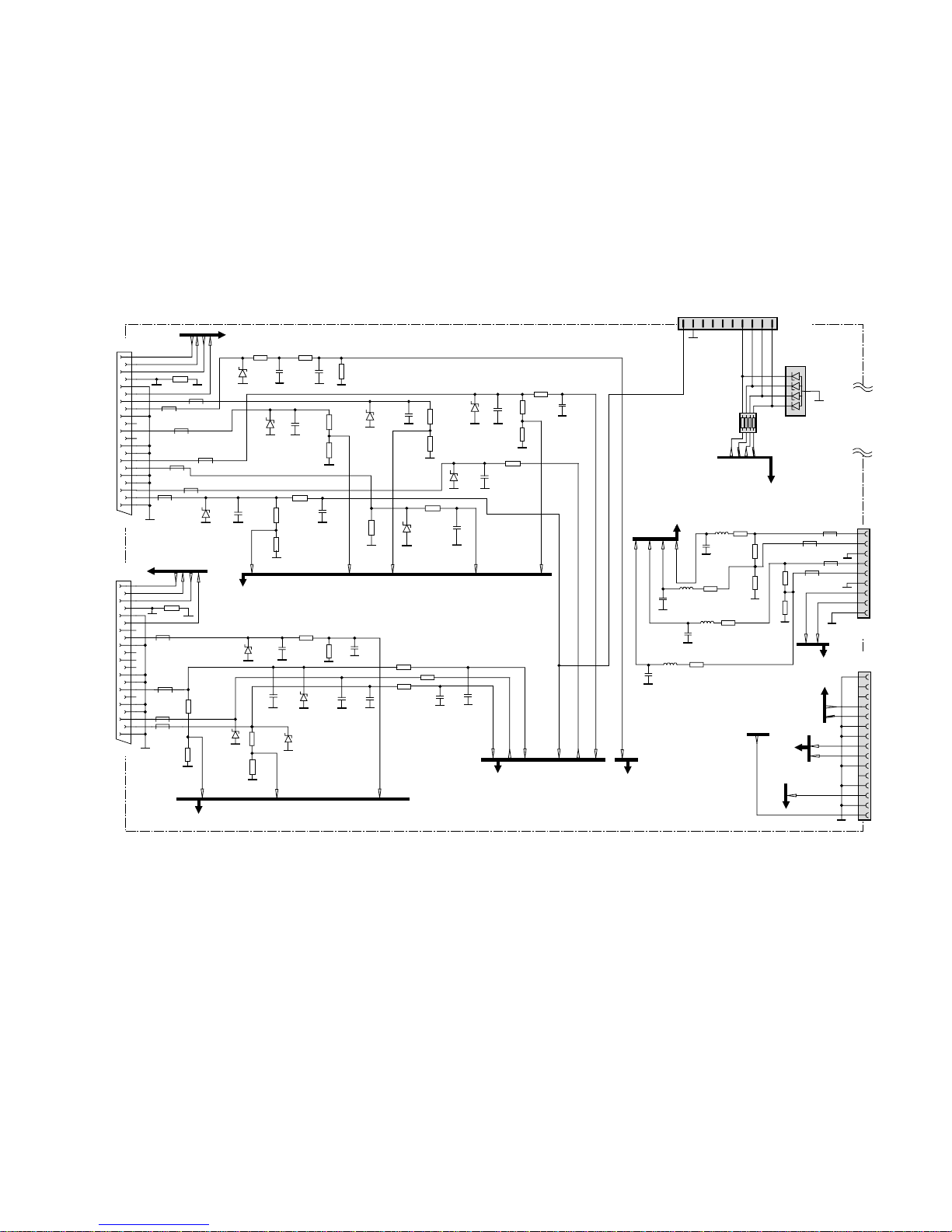
MAIN SCHEMATIC DIAGRAM - SCHEMA DE LA PLATINE PRINCIPALE - SCHALTBILD HAUPTPLATINE - SCHEMA DELLA PIASTRA PRINCIPALE- ESQUEMA DE LA PLATINA PRINCIPAL
Page 24
EFC031-IFC130-IFC230
First issue 12/05
VIDEO SWITCHING
DIGITAL INTERFACE
SCH IFC130E AV BOARD
10
11 12
13 14
15 16
17 18
19
2
20
21 22
23 24
25 26
27 28
29
3
30
31 32
33 34
35 36
37 38
39
4
40
41 42
43 44
45 46
47 48
56
78
9
1
49
51
53
55
57
59
50
52
54
56
58
60
61
63
65
67
62
64
66
68
69 70
71 72
73
75
74
76
77
79
78
80
BX100
80-WAY
CX702
0R
RX703
75R
D_CVBS
I2C0/1_CLK
I2C0_CLK
I2C0/1_DATA
I2C0_DATA
COMP_R_IN
JX001
0R
CVBSOUT_AV1_CTRL
CVBSOUT_AV2_CTRL
MASTER_MUTE
COMP_L_IN
AV1_CVBS/Y_IN
AV1_PIN8_OUT_6
AV1_PIN16
AV1_RED/C_IN
AV1_GREEN
AV1_PIN8_IN
AV1_BLUE
AV2_CVBS/Y_IN
CVBS_AV2_OUT2
AV1_PIN8_OUT_12
AV2_C_IN
DGND
MA_TUNER_CVBS
DGND
C_AV_IN
Y_AV_IN
YC_SEL_CTRL1AV3/F_CHROMA_IN
AV3/F_CVBS_IN
VGA_R_IN
VGA_L_IN
AUDIO_STBY
CR_R_IN
RESET_AUDIO
CR_L_IN
DVI_R_IN
DVI_L_IN
LINE_O/P_R
BCLK
LINE_O/P_L
LRCLK
PCMDATA0
I2C2_CLK
I2C2_DATA
0R
JX706
0R
JX702
0R
JX701
0R
JX705
0R
JX710
0R
JX713
0R
JX703
0R
JX704
I2C1_CLKI2C1_DATA
AGND
DGND
YC_SEL_CTRL2
JX003
0R
JX002
0R
0R
JX004
AGND
METAL_GND
150R
RX701
150R
RX700
47P
CX700
47P
CX701
RX704
75R
LX700
600
LX701
600
AGND
AGND
AGND
AGND AGND
D_Y
D_CHR
YC_DVD_SEL_CTRL
MAIN SCHEMATIC DIAGRAM - SCHEMA DE LA PLATINE PRINCIPALE - SCHALTBILD HAUPTPLATINE - SCHEMA DELLA PIASTRA PRINCIPALE- ESQUEMA DE LA PLATINA PRINCIPAL
Page 25
EFC031-IFC130-IFC230
First issue 12/05
GND
OUT
IN
GND
OUT
IN
OUT
IN
GND
GND
OUT
IN
+24V
+12V_UA
+24V_GND
+12V_GND
+6V5
VOLTAGE REGULATOR
1
2
3
4
5
6
7
8
9
10
11
12
13
14
BP100
+24V
+12V
SCH IFC130E AV BOARD
CP110
220N
16V
RP105
560R
16V
100UF
CP104
1
2
3
LD1117DT
ICS
IP103
JP104
0R
JP105
0R
JP106
0R
RP106
3K9
CP105
100UF
16V
3
1
2
KF80BDT
IP104
220N
16V
CP109
16V
220N
CP108
CP116
100UF
16V
220N
CP107
16V
16V
100UF
CP106
220N
CP115
16V
CP101
100UF
16V
220N
CP111
CP102
100UF
16V
2
3
1
LF50CDT
IP106
CP112
220N
16V
10U
CP118
JP002
0R
JP001
0R
0R
JP003
1
2
3
IP101
LD1117DT33
AGND
GND
+24V_GND
+24V_GND
3V3
GND
GND
+12V_GND
8V
5V
10V
+12V_OUT
AGND
+12V_GND
+12V_UA
+12V_UA
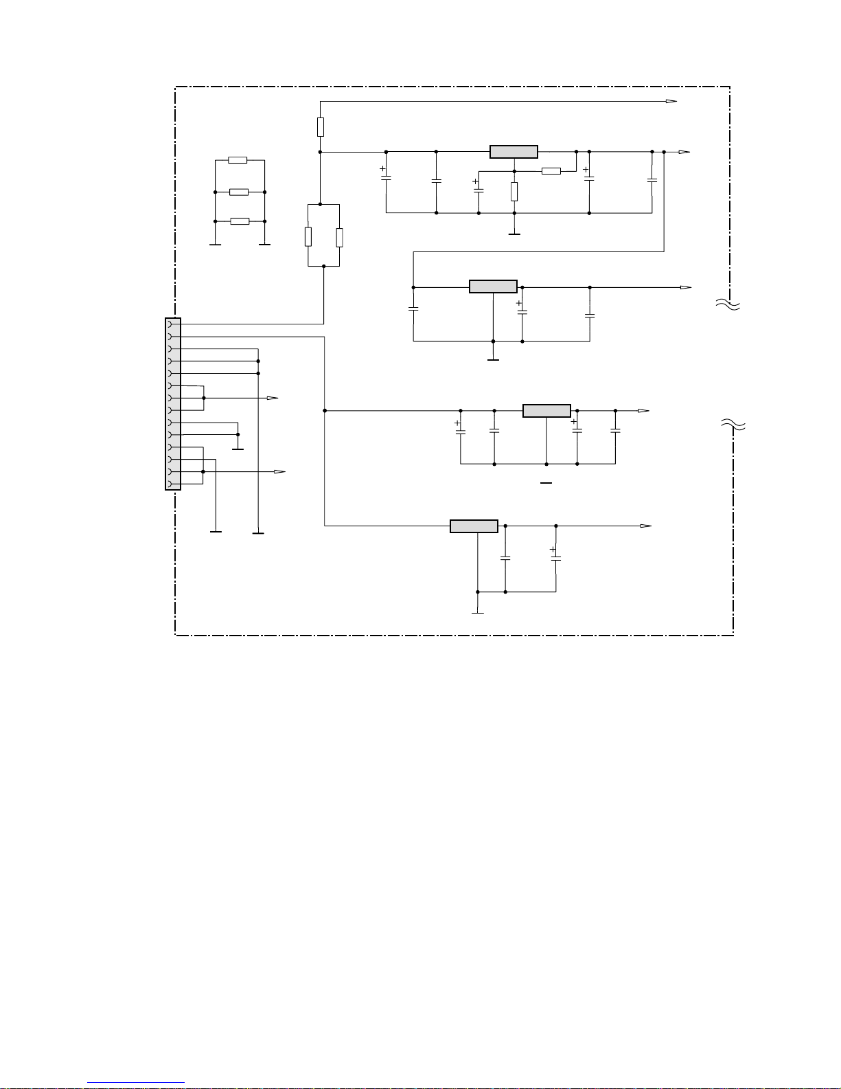
MAIN SCHEMATIC DIAGRAM - SCHEMA DE LA PLATINE PRINCIPALE
SCHALTBILD HAUPTPLATINE - SCHEMA DELLA PIASTRA PRINCIPALE
ESQUEMA DE LA PLATINA PRINCIPAL
Page 26
EFC031-IFC130-IFC230
First issue 12/05
STA515W
OUT2B2
GND2B
GNDSUB
OUT2B1
VCC2B
VCC1A
OUT1A1
OUT1A2
GND1A
IN1A
GND1B
OUT1B2
OUT1B1
VCC1B
VCC2A
OUT2A1
OUT2A2
GND2A
TH-WAR
IN1B
VL
CONFIG
PWRDN
TRI-STATE
FAULT
VDD2
IN2B
GND-CLEAN
GND-REG
IN2A
VCCSIGN1
VCCSIGN2
VSS1
VSS2
VDD1
NC
M14
M16
M3
M2
M5
M4
M17
M15
PROTECTION
&
LOGIC
REGULATORS
AUDIO AMP
SCH IFC130E AV BOARD
AUDIO_STBY1
TS203
RN1402
DS204
IN4148
DS201
IN4148
DS203
IN4148
RS201
10K
TS202
BC856B
DS213
DS212
DS211
DS210
CS205
100N
1K
RS222
47K
RS202
CS232
1MI0F
18R
RS212
2
5
1
3
4
15
17
16
14
29
13
10
11
12
7
8
9
6
28
30
23
24
25
26
27
21
32
19
20
31
36
35
34
33
22
18
IS200
GND
CS220
1UF
CS218
1UF
CS215
470N
5R6
RS210
CS212
100N
CS211
100N
CS207
100N
CS208
100N
0R
JS001
PWM_RM
PWM_RP
PWM_LP
RS220
0R
+24V_GND
+24V_GND
RS208
10R
CS216
680P
+24V_GND
RS209
10R
CS217
680P
+24V_GND
CS219
1UF
LS213
1000 OHM
1
2
3
4
5
6
BS002
LS211
1000 OHM
0R
RS257
LS210
1000 OHM
0R
RS254
0R
RS255
0R
RS256
LS212
1000 OHM
VALIED_LR
0R
RS250
LS204
22UH
LS203
22UH
LS202
22UH
LS201
22UH
CS230
470UF
CS201
470UF
AGND
0R
JS003
0R
JS002
GND
0R
JS004
+24V_GND
DS207
IN4148
CS203
100N
CS214
470N
CS213
100N
CS210
100N
CS209
100N
CS206
100N
CS204
100N
CS202
100N
CS221
1UF
5R6
RS211
18R
RS213
+24V_GND
+24V_GND
+24V_GND
+24V_GND
+24V_GND
+24V_GND
+24V_GND
+24V_GND
0R
JS005
GND
GND
DGND
GND
+24V_GND
3V3
PWM_LM
AUDIO_STBY
+24V
+24V_GND
+24V_GND
+24V_1
L/R_MUTE
+24V_GND
HP_DET
MASTER_MUTE
RS251
470R
MAIN SCHEMATIC DIAGRAM - SCHEMA DE LA PLATINE PRINCIPALE - SCHALTBILD HAUPTPLATINE - SCHEMA DELLA PIASTRA PRINCIPALE- ESQUEMA DE LA PLATINA PRINCIPAL
Page 27
EFC031-IFC130-IFC230
First issue 12/05
AGNDC
NC1
SC4_IN_L
SC4_IN_R
ASG1
SC3_IN_L
AVSS1
NC2
AVSUP2
ANA_IN1+
ANA_IN-
ANA_IN2+
STANDBYQ
D_CTR_I/O_0
XTAL_OUT
XTAL_IN
D_CTR_I/O_1
SPDIF_OUTTPVALIED_LR
AUD_CL_OUT
VALIED_B
ADR_SEL
TESTEN
AVSUP1
AVSS
SC5_IN_R
VREFTOP
SC5_IN_L
SC2_IN_L
ASG2
SC3_IN_R
I2S_WS
I2S_DA_OUT
I2S_DA_IN1
I2S_DEL_IN
I2S_DEL_OUT
I2S_DEL_CL
I2S_DEL_WS
DVSUP1
DVSUP2
DVSS1
DVSS2
DVSS3
I2S_DA_IN2
I2S_CL3
I2S_WS3
RESETQ
I2S_DA_IN3
I2S_DA_IN4
DACA_R
DACA_L
PWM_BM
PWM_BP
PWM_VDD
VREF2
PWM_VSS
PWM_RM
PWM_RP
PWM_LM
PWM_LP
SC2_OUT_R
SC2_OUT_L
VREF1
SC1_OUT_R
SC1_OUT_L
CAPL_A
AHVSUP
SC3_OUT_R
SC3_OUT_L
AHVSS1
AHVSS2
SC2_IN_R
ASG3
SC1_IN_L
SC1_IN_R
I2C_DA
I2S_CL
I2C_CL
SHUTDOWNQ
MSP46XYK
ROUT2
NCNCL5
L4
L3L2VS
GND
NC
NC
L6
LOUT2
ROUT1
LOUT1
LOUT3
ROUT3
L1 R1
R2R3R4R5R6
CAPA
ADDR
SCL
SDA
AUDIO MSP
component location close to connectors
ESDA14V2L
IA301
CA303
470U0
SCH IFC130E AV BOARD
TA003
RN2042
GND
1N0
CA003
AUDIO_STBY
GND
1
2
3
4
BA301
LRCLK
PCMDATA0
BCLK
15K0
RA001
GND
PWM_LP
PWM_LM
PWM_RP
PWM_RM
RA015
470R0
1U8H
LA004
MUTE
VALIED_LR
VALIED_B
GND
CA036
10U0
CA304
1UF
CA300
1UF
CA052
1N0
4U7
CA024
0R
RA275
CA009
220N0
0R
RA273
LA001
4U7
LA005
4U7
0R
RA274
LA010
4U7
47R0
RA002
RA012
100R0
RA011
100R0
47UF
CA262
45
46
47
48
49
50
62
63
656667
68
80
78
71
70
77
7672757374
79
69
64
61
60
58
59
53
52
51
5
6
7
8
9
10
11
12
13
14
15
16
17
18
19
20
21
22
23
24
262728252930313233343536373839
40
41
42
43
44
54
55
56
57
1
2
3
4
IA001
470R0
RA277
470R0
RA276
47UF
CA252
47UF
CA225
RA008
100R0
RA009
100R0
47UF
CA273
RA020
1K0
RA021
1K0
GND
CA021
47P0
RA019
1K0
CA025
1UF
COMP_L_IN
100N0
CA023
RA022
1K0
GND
CA022
47P0
COMP_R_IN
CA026
1UF
CA027
1UF
AV2_L_IN
CA029
47P0
CA028
1UF
AV2_R_IN
GND
CA030
47P0
1K0
RA023
AV1_L_IN
CA031
1UF
1K0
RA024
GND
47P0
CA033
CA032
1UF
AV1_R_IN
CA035
100N0
1N0
CA038
RA025
1K0
CA037
1UF
AM_AF
GND
47P0
CA002
RA018
47R0
47R0
RA016
GND
470P0
CA008
GND
180P0
CA019
CA020
180P0
1K0
RA013
1K0
RA014
CA524
1UF
CA517
1UF
GND
GND
RA320
18K0
HP_DET
5V
RA310
18K0
5V
HP_R_IN_FCB
I2C0/1_DATA
I2C0/1_CLK
AV1_R_OUT
AV1_L_OUT
47UF
CA265
AV2_L_OUT
AV2_R_OUT
AV1_L_OUT
AV1_R_OUT
DVI_L_IN
DVI_R_IN
CA518
47UF
100U0
CA048
CA305
470U0
10U0
CA302
10U0
CA306
16V
470UF
CA042
10U0
CA060
10U0
CA012
CA014
10U0
47UF
CA520
CA505
1UF
CA519
100N0
FCB_R_IN
10V
GND
GND
GND
1N0
CA011
GND
GND
CA010
100N0
GND
GND
GND
GND
12457
1011121314 15
16171819202122232526272824
638
9
IA500
TEA6422D
TA001
BC846B
TA002
BC846B
LA301
300R0
10V
3V3
GND
GND
1N0
CA507
100K0
RA505
DVD_L_IN
GND
CA016
470P0
GND
470P0
CA015
470P0
CA007
CA061
100N0
CA062
100N0
LA300
300R0
4R7
RA303
MASTER_MUTE
RESET_AUDIO
3K9
RA300
100R0
RA003
1N0
CA051
RA305
3K9
RA312
18K0
RA304
10K0
RA302
18K0
RA307
18K0
100K0
RA306
4
8
7
5
6
100R0
RA004
GND
AUDIO_STBY
47R0
RA500
47R0
RA501
FCB_L_IN
15U0
LA002
LA003
15U0
470R0
RA017
VGA_R_IN
VGA_L_IN
SIF
18M432
QA001
3P3
CA046
CA045
47P0
CA040
100P0
100N0
CA521
100N0
CA043
PG
2
3
1
8
4
IA300
TS482D
CA044
10N0
GND
CA039
100P0
RA502
100K0
CA514
1N0
GND
47P0
CA001
GND
1K0
RA026
4R7
RA309
CA049
1N0
GND
GND
GND
GND
8V
100N0
CA050
3P3
CA047
CA041
220N0
CA034
47P0
100N0
CA307
100K0
RA301
RA308
10K0
GND
GND
GND
GND
GND GND
GND
DVD_R_IN
GND
GND
GND
GND
GND
GND
GND
GND
GND
GND
L/R_MUTE
SUB_MUTE
GND
GND
GND
LA211
300
RA212
4K7
CA210
220P0
LA210
300
4K7
RA210
LA201
300
4K7
RA202
220P0
CA200
RA200
4K7
LA200
300
47K0
RA203
RA201
47K0
220P0
CA201
RA213
47K0
CA212
220P0
CA203
220P0
220P0
CA202
220P0
CA213
47K0
RA211
CA211
220P0
GND
L_IN_AV2
AV2_L_IN
AV1_R_IN
R_IN_AV2
GND
GND GND GND
GNDGND
GND GND
L_IN_AV1
R_IN_AV1
GND GND
AV1_L_IN
GND
AV2_R_IN
LA261
LA260
LA251
LA250
220R0
RA250
220R0
RA252
47K0
RA253
CA260
1N0
47K0
RA251
470P0
CA251
1N0
CA250
RA260
220R0
RA261
47K0
CA261
470P0
CA254
470P0
1N0
CA253
CA263
1N0
RA263
47K0
470P0
CA264
RA262
220R0
L_OUT_AV2
R_OUT_AV2
L_OUT_AV1
GND
GNDGNDGND
GND
GND
GND GND
GND
GND
GND
GND
R_OUT_AV1
GND
CA501
1UF
CA502
1UF
CA506
1UF
CA515
1UF
CA522
1UF
CA516
1UF
CA503
1UF
1
2
3
BA300
GND
HP_L_IN_FCB
DA301
IN4148
LINE_O/P_R
LINE_O/P_L
470P0
CA274
RA272
100R0
GND
47UF
CA271
470P0
CA272
RA271
100R0
GND
AV2_R_OUT
AV2_L_OUT
3V3
5V
8V
GND
MAIN SCHEMATIC DIAGRAM - SCHEMA DE LA PLATINE PRINCIPALE - SCHALTBILD HAUPTPLATINE - SCHEMA DELLA PIASTRA PRINCIPALE- ESQUEMA DE LA PLATINA PRINCIPAL
Page 28
EFC031-IFC130-IFC230
First issue 12/05
+33V
+5V-IF
+5V-T
AGC
AS
AUDIO
FM-I F
FM-SW
GND
NC2
SCL
SDA
SIF
VIDEO
NC3
NC4
NC5
o/p
(int)
+5V-T
FMinput
NC1
IN
OUT
+33V
+5V-IF
+5V-T
AGC
AS
AUDIO
FM-IF
FM-SW
GND
NC2
SCL
SDA
SIF
VIDEO
NC3
NC4
NC5
o/p
(int)
+5V-T
FMinput
NC 1
(MAIN-TUNER) (SLAVE-TUNER)
33Vdc Invertor
To AV Board
2T RF TUNER
SCH 2T RF MODULE IFC130/230
123456789101112131415
BH101
10U0
LH005
5VT
RH051
0R
8
123
4
9
131415
16
5
6
121011
7
171819
20
NH001FE6233
AGND
AGND
AGND
CH106
220U
10V
+6V5
JH108
0R
LH003
10U0
I2C0_DATA
I2C0_CLK
5V
RH009
2K7
3
2
1
LD1117S50C
IH100
AM_AF
RH006
6K8
RH007
180R0
JH107
5V
5VT
TH100
BC846B
CH050
120P
RH017
91R
5VT
0R
JH106
0R
JH102
DH101
BZX55B33
33V
JH104
0R
0R
JH105
0R
JH101
SIF
RH008
0R
RH103
22R
50V
CH019
1UF
RH101
150R
AGND
CH102
180P
CVBS_IFM
JH003
0R
JH002
0R
JH001
0R
33VT
AGND
AGND
AGND
AGND
AGND
AGND
AGND
AGND
AGND
AGND
AGND
AGND
16V
CH006
100UF
CH005
22N0
RH003
1K0
LH050
3U3H
33VT
RH100
10K
10UH
LH002
CH002
1N0
LH001
10U0
RH010
1K5
33P0
CH009
16V
CH007
47UF
RH102
10K
LH100
1MH
RH050
0R
CH101
10N
50V
CH100
22N
CH018
330P0
CH008
33P0
CH004
22N0
1N0
CH003
1N0
CH001
TH001
BC846B
RH011
47R0
RH005
100R0
100R0
RH004
220N
CH107
16V
DH100
BA592
CH105
6N8
CH103
4N7
16V
1UF
CH104
AGND METAL_GND
0R
JH004
AGND
AGND
AGND
LH004
10U0
CH120
220U
10V
AGND
8
123
4
9
131415
16
5
6
121011
7
171819
20
NH002FE6232
33P0
CH013
CH012
33P0
16V
100UF
CH016
22N0
CH015
RH015
2K
2
RH012
0R
1N0
CH011
91R
RH016
10U0
LH007
CH051
120P
100R0
RH014
RH013
100R0
LH006
10UH
CH010
1N0
16V
100UF
CH017
LH051
3U3H
22N0
CH014
AGND
33VT
5VT
AGND AGND
AGND
AGND
AGND
AGND
AGND
AGND
AGND
AGND
AGND
AGND
AGND
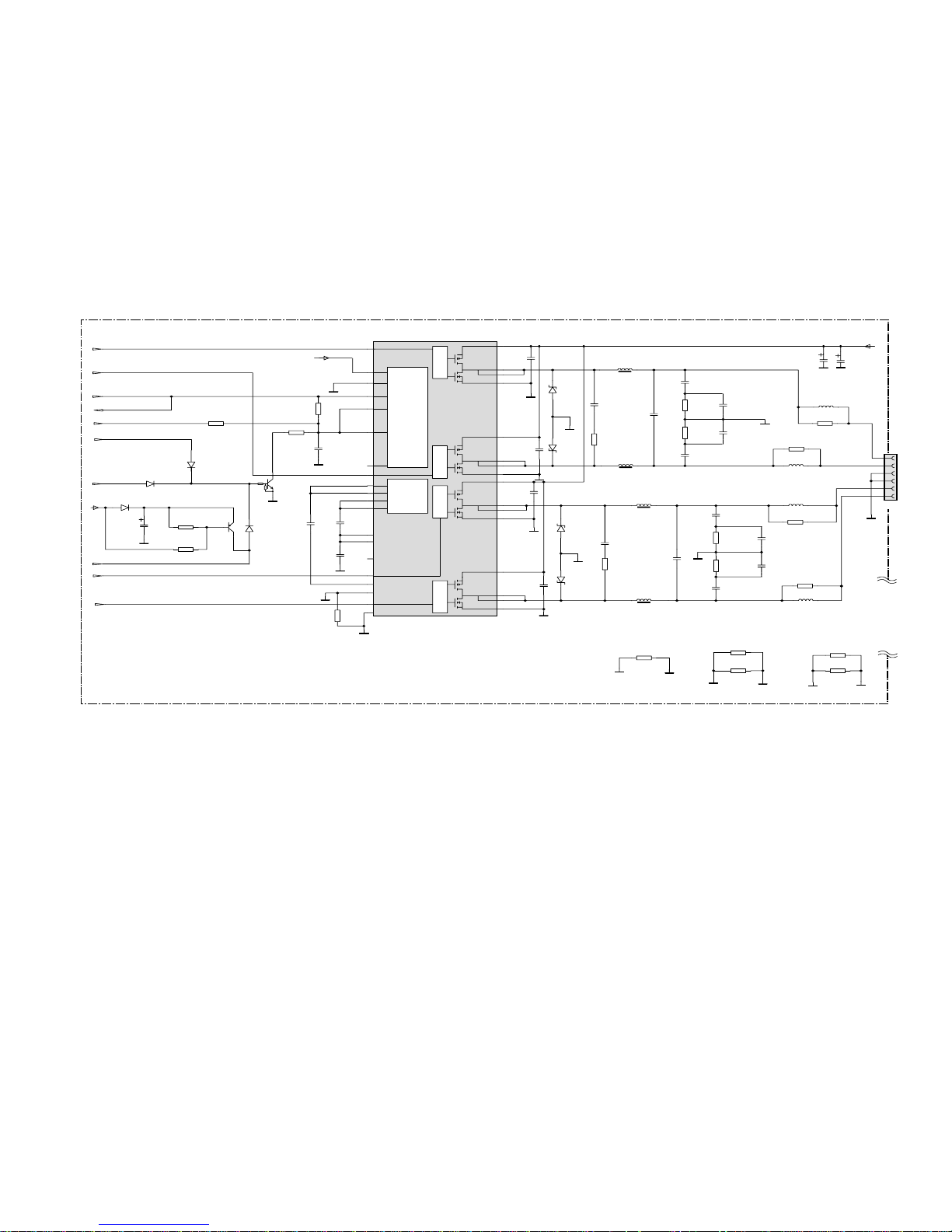
MAIN SCHEMATIC DIAGRAM - SCHEMA DE LA PLATINE PRINCIPALE - SCHALTBILD HAUPTPLATINE - SCHEMA DELLA PIASTRA PRINCIPALE- ESQUEMA DE LA PLATINA PRINCIPAL
Page 29
EFC031-IFC130-IFC230
First issue 12 / 05
SCALER SCHEMATIC DIAGRAM - SCHEMA DE LA PLATINE SCALER - SCHALTBILD SCALER - SCHEMA DELLA PIASTRA SCALER - ESQUEMA DE LA PLATINA SCALER
Page 30
EFC031-IFC130-IFC230
First issue 12 / 05
SCALER SCHEMATIC DIAGRAM - SCHEMA DE LA PLATINE SCALER - SCHALTBILD SCALER - SCHEMA DELLA PIASTRA SCALER - ESQUEMA DE LA PLATINA SCALER
Page 31

EFC031-IFC130-IFC230
First issue 12 / 05
SCALER SCHEMATIC DIAGRAM - SCHEMA DE LA PLATINE SCALER - SCHALTBILD SCALER - SCHEMA DELLA PIASTRA SCALER - ESQUEMA DE LA PLATINA SCALER
Page 32

EFC031-IFC130-IFC230
First issue 12 / 05
SCALER SCHEMATIC DIAGRAM - SCHEMA DE LA PLATINE SCALER - SCHALTBILD SCALER - SCHEMA DELLA PIASTRA SCALER - ESQUEMA DE LA PLATINA SCALER
Page 33

EFC031-IFC130-IFC230
First issue 12 / 05
SCALER SCHEMATIC DIAGRAM - SCHEMA DE LA PLATINE SCALER - SCHALTBILD SCALER - SCHEMA DELLA PIASTRA SCALER - ESQUEMA DE LA PLATINA SCALER
Page 34

EFC031-IFC130-IFC230
First issue 12 / 05
SCALER SCHEMATIC DIAGRAM - SCHEMA DE LA PLATINE SCALER - SCHALTBILD SCALER - SCHEMA DELLA PIASTRA SCALER - ESQUEMA DE LA PLATINA SCALER
Page 35

EFC031-IFC130-IFC230
First issue 12 / 05
SCALER SCHEMATIC DIAGRAM - SCHEMA DE LA PLATINE SCALER - SCHALTBILD SCALER - SCHEMA DELLA PIASTRA SCALER - ESQUEMA DE LA PLATINA SCALER
Page 36

EFC031-IFC130-IFC230
First issue 12 / 05
SCALER SCHEMATIC DIAGRAM - SCHEMA DE LA PLATINE SCALER - SCHALTBILD SCALER - SCHEMA DELLA PIASTRA SCALER - ESQUEMA DE LA PLATINA SCALER
Page 37

27LB052B5 Version 1
MODULES
SCAL SCALER (CMO270W1-5V) R=Y
21642140
AV AV IFC130E R=Y
21630830
FAV FAV IFC130E 01 R=Y
2145075A
IF RF IFC130E 01 R=Y
2146366A
KB KB/IR/LED IFC130E R=Y
21450300
POWE SMPS (POWER MAIN) R=Y
56033370
PWSB SMPS (STANDBY) R=Y
2143065A
I
DT100 ESD CM1213-02SR R=Y
56153310
FZP00 TE5-T NO396 1600MA 125V W
56073850
R=Y
FZP11 TE5-T NO19396 2.5A 125V W
21210080
R=Y
IA001 MSP4610K-QA-D6-002 FLAT
21429440
R=Y
IA300 TS482D FLAT R=Y
10938190
IA301 ESDA14V2L R=Y
10938390
IA500 TEA6422D FLAT R=Y
10938180
ID100,101 MT46V16M16P-6T FLAT R=Y
56047800
IH100,IP101 LD1117S50C FLAT R=Y
21431700
IP100,103,107, LD1117S33TR FLAT R=Y
21408040
110,121
IP101 LD1117DT33 R=Y
10938450
IP102,105 LD1086D2T18 FLAT R=Y
15704470
IP103 LD1117DT** FLAT R=Y
36002660
IP104 KF80BDT R=Y
10938410
IP104 LD1117S18TR FLAT R=Y
10838530
IP106 LF50CDT FLAT R=Y
10938460
IP106 LD1117S25TR FLAT R=Y
10796380
IP108,109 L4973D5.1 FLAT R=Y
21423050
IP610 STR-A6159 R=Y
21429400
IP620 TL431 R=Y
36032720
IP630 TCET1103G R=Y W
10547560
IR100 PW118B-10L FLAT R=Y
56262220
IR103 PST421A290N FLAT R=Y
21336420
IR105 M24C64-WMN6 FLAT R=Y
10937970
IR106 M29W320EB70N6 SOFT W
2164188A
BN1.02 FLAT R=Y
IR200 74LVX574 FLAT R=Y
56002110
IR900 DS90C387AVJD FLAT R=Y
21421160
IS200 STA515W FLAT R=Y
21428980
IT100 SII9011CTU FLAT R=Y
21426190
IT101 UPA672T-T1-A FLAT R=Y
16401240
IT105,106,107 ESD CM1213-04SO R=Y W
55983920
IT150,IV300 M24C02-WMN6TP(BLANK)
20940740
FLAT R=Y
IV200 PW2300-30L FLAT R=Y
56262240
IV201 MT48LC4M16A2TG-7EG FLAT
2127609A
R=Y
IV301 ESD PACVGA105QR R=Y W
56329710
IV302 RS232 FLAT R=Y
21380590
IV700 SAA7117A FLAT R=Y
21427270
IX802 TEA6415CD FLAT R=Y
56094390
IX803,805 MM1511XNRE FLAT R=Y
55489750
IX807 MM1224XFBE FLAT R=Y
21429890
IX808 MM11228XF FLAT R=Y
55175740
T
IR102 STT4PF20V SMD R=Y W
21393360
TA001,002, BC846B SMD R=Y
16006260
TH001,100,
TK001
TA003 RN2402 SMD R=Y
16007110
TP601 BC848B SMD R=Y
36030440
TS202 BC857B SMD R=Y
16564890
D
DE101 NSAD500H R=Y
16100970
DH100 BA592 SMD R=Y
36087890
DH101 BZX55C33 R=Y
36030740
DP101,105,106, FM220-M SMD R=Y
56008310
114,115,116,
DT152
DP102,103,107, FM201 SMD R=Y
56008320
110,111
DP108,109,616 SB560 5A/60V R=Y
36095130
DP601,DS203, LL4148 SMD R=Y
36103600
207,216,218
DP611,612,613, FS1MI 1KV 1A R=Y
56033250
614
DP615 FUF4005/MUR160 R=Y
16009580
DP617 RGP15G R=Y
36044080
DT104 MMSZ3V3T1 SMD R=Y
15580410
DT150 BZT52C5V6 SMD R=Y
15583660
DV200,201,202, MMSZ6V8T1 SMD R=Y
15580490
DX100,101,102,
103,104,105,
201,202,206
DV300 BAV70-V SMD R=Y
36011610
DV308,309,310, BAV99 R=Y
16345680
311
DV502,600,601, ZMM6,8 SMD R=Y
16030380
602
DX106,200 MMSZ15T1 SMD R=Y
15580570
GE001 1259-7VRVGW LED R=Y
21393660
TK002,TR100, RN1402 SMD R=Y
36042230
101,TS203,205,
TT120,121
F
QA001 18M432HZ R=Y
10334670
QR100 14M31818HZ SMD R=Y
25730230
QT100 28M322HZ SMD R=Y
56055930
QV200 27M0HZ SMD R=Y
56049260
QV700 32M11KHZ SMD R=Y
56025920
THOMSON
27LB052B5
Chassis IFC130
PARTS LIST
LISTE PIECES DETACHEES
ERSATZTEILLISTE
LISTA PARTI DI RICAMBIO
LISTA DE PIEZAS DE REPUESTO
TV
No copying, translation, modification on other use authorized. All rights reserved worldwide. • Tous droits de reproduction, de traduction, d'adaptation et d'exécution réservés pour tous les pays. • Sämtliche Urheberrechte an diesen Texten und Zeichnungen stehen uns zu. Nachdrucke,
Vervielfältigungen - auch auszugsweise - nur mit unserer vorherigen Zustimmung zulässig. Alle Rechte vorbehalten. • I diritti di riproduzione, di traduzione, e esecuzione sono riservati per tutti i paesi. • Derechos de reproduccion, de traduccion, de adaptacion y de ejecucion reservados para todos los paises.
For any requests, please contact THOMSON after sales europe area
Pour toutes précisions, contactez votre service apres vente local THOMSON service europe
Für weitere Auskünfte, wenden Sie sich bitte an die THOMSON sales europe Kundendienste
Per precisazioni, contattare l’assistenza tecnica THOMSON sales europe
Para cualquier pregunta, por favor contactar con el responsable de zona del servicio postventa de THOMSON sales europe
VERSION 1 04 / 2006
36114970
VERSION 2 06 / 2006
1/6
Lead Free
Sans Plomb
R=Y ohne blei
senza cavo
sin plomo
CMO V270W1-L04 Version 1 :
27LB052B51
CMO V270B1-L01 Version 2 :
27LB052B52
Page 38

LJ705 CABLE V270W1-LO4 WITH
56060420
CARD READER CONNECTOR
CABLE V270W1-LO4 AVEC
CARD READER CONNECTEUR
KABEL V270W1-LO4 MIT
CARD READER VERBINDER
CAVO V270W1-LO4 CON
CARD READER CONNETTORE
CABLE V270W1-LO4 CON
CARD READER CONECTOR
NH001 FE6232B TUNER R=Y
21634740
FE6232B TETE R=Y
FE6232B TUNER R=Y
FE6232B TUNER R=Y
FE6232B SINTONIZADOR R=Y
SK001,002,003, MICROSWITCH R=Y
36083570
004,005,006 MICRO CONTACTEUR R=Y
MIKROSCHALTER R=Y
MICROINTERRUTTORE R=Y
MICROCONTACTOR R=Y
SP600 RELAY 6.0V 68.0OHM W
10517140
10.0A 250.0V R=Y
RELAIS 6.0V 68.0OHM
10.0A 250.0V R=Y
RELAIS 6.0V 68.0OHM
10.0A 250.0V R=Y
RELE 6.0V 68.0OHM
10.0A 250.0V R=Y
RELE 6.0V 68.0OHM
10.0A 250.0V R=Y
EQUIPMENT/PRESENTATION
EQUIPEMENT/PRESENTATION
AUSSTATTUNG/GEHAEUSE
PARTI VARIE
EQUIPO/PRESENTACION
DISPLAY LCD 27 V270W1/L04 C4 CMO
2574231A
ECRAN LCD 27 V270W1/L04 C4 CMO
LCD-ANZEIGE 27 V270W1/L04 C4 CMO
VISUALIZZATORE LCD 27 V270W1/L04 C4 CMO
VISUALIZADOR LCD 27 V270W1/L04 C4 CMO
FRONT PANEL BK25RCT
56311610
FACADE BK25RCT
FRONTPLATTE BK25RCT
PANNELLO FRONTAL BK25RCT
PANEL FRONTAL BK25RCT
BASE PLATE OF THE FOOT
25831520
EMBASE DU PIED
FUSS-BASISPLATTE
BASE DI APPOGGIO DEL PIEDE
EMBASE DEL PIE
SCREW-PLAST 4MM 10MM
25540390
VIS-PLAST 4MM 10MM
SCHRAUBE 4MM 10MM
VITE 4MM 10MM
TORNILLO 4MM 10MM
LID OF FOOT SI01TH
56311590
COUVERCLE DU PIED SI01TH
KAPPE DES FUSSES SI01TH
COPERCHIO DEL PIEDE SI01TH
TAPA DEL PIE SI01TH
SCREW 6MM 12MM
25815390
VIS 6MM 12MM
SCHRAUBE 6MM 12MM
VITE 6MM 12MM
TORNILLO 6MM 12MM
REAR PANEL AL01TH R=Y
25803920
DOS AL01TH R=Y
RUECKWAND AL01TH R=Y
PANNELLO POSTERIORE AL01TH R=Y
TAPA POSTERIOR AL01TH R=Y
LED WINDOW
25804080
GLACE LED
FENSTER LED
VETRO LED
CRISTAL LED
C
CP602 220N0F 20% 275V R=Y W
56354950
CP610 150P0F 10% 1K0V R=Y
56104630
CP611 22U0F 20% 400V R=Y
56059780
CP612,617 1N0F 20% 1K0V R=Y
36031000
S
LP610 TFSMT1W R=Y W
2142952A
OTHER PARTS
AUTRES PIECES
SONSTIGE TEILE
ALTRE PARTI
OTRAS PIEZAS
BA600 HEADPHONE SOCKET R=Y
56021170
PRISE CASQUE R=Y
KOPFHOERERBUCHSE R=Y
PRESA JACK R=Y
TOMA JACK R=Y
BA700,800 CINCH SOCKET 2 ASSY R=Y
56009180
ENSEMBLE 2 PRISES CINCH R=Y
CHINCH 2 BUCHSEN-EINHEIT R=Y
ASSIEME 2 PRESA CINCH R=Y
CONJUNTO 2 TOMA CINCH R=Y
BH101 CABLE FLAT 15 50MM B8 R=Y
56115260
CABLE NAPPE 15X 50MM B8 R=Y
FOLIENKABEL 15X 50MM B8 R=Y
CAVO DI COLLEGAMENTO
15X 50MM B8 R=Y
CABLE 15X 50MM B8 R=Y
BK102 CABLE FLAT 5X 250MM R=Y W
56084990
CABLE NAPPE 5X 250MM R=Y
FOLIENKABEL 5X 250MM R=Y
CAVO DI COLLEGAMENTO
5X 250MM R=Y
CABLE 5X 250MM R=Y
BQ01 JACK SOCKET R=Y W
21428320
PRISE JACK R=Y
JACK-BUCHSE R=Y
PRESA JACK R=Y
TOMA JACK R=Y
BS903 CINCH SOCKET R=Y
10037440
PRISE CINCH R=Y
CINCH-BUCHSE R=Y
PRESA CINCH R=Y
TOMA CINCH R=Y
BT100 HDMI SOCKET R=Y
1621655C
PRISE HDMI R=Y
HDMI-BUCHSE R=Y
PRESA HDMI R=Y
TOMA HDMI R=Y
BV300 VGA SOCKET R=Y
10494890
PRISE VGA R=Y
VGA-BUCHSE R=Y
PRESA VGA R=Y
TOMA VGA R=Y
BV400 SVHS SOCKET R=Y
20392900
PRISE SVHS R=Y
S-VHS-BUCHSE R=Y
PRESA SVHS R=Y
TOMA SVHS R=Y
BV500 CINCH SOCKET 3 ASSY R=Y
56009160
ENSEMBLE 3 PRISES CINCH R=Y
CHINCH 3 BUCHSEN-EINHEIT R=Y
ASSIEME 3 PRESA CINCH R=Y
CONJUNTO 3 TOMA CINCH R=Y
BV600 CINCH SOCKET 3 ASSY R=Y
56009170
ENSEMBLE 3 PRISES CINCH R=Y
CHINCH 3 BUCHSEN-EINHEIT R=Y
ASSIEME 3 PRESA CINCH R=Y
CONJUNTO 3 TOMA CINCH R=Y
BX101,200 SCART SOCKET R=Y W
21428350
PRISE PERITEL R=Y
EURO-AV-BUCHSE R=Y
EUROPRESA NORMALIZZATA R=Y
EUROCONECTOR R=Y
FP610 FUSE HOLDER R=Y
10260630
SUPPORT FUSIBLE R=Y
SICH-HALTER R=Y
PORTA FUSIBILE R=Y
PORTA FUSIBLE R=Y
FP610 500MA 250V FUSE R=Y W
48029700
500MA 250V FUSIBLE R=Y
500MA 250V SICHERUNG R=Y
500MA 250V FUSIBILE R=Y
500MA 250V FUSIBLE R=Y
LJ050 CABLE FLAT 6X 650MM
56047000
CABLE NAPPE 6X 650MM
FOLIENKABEL 6X 650MM
CAVO DI COLLEGAMENTO
6X 650MM
CABLE FLAT 6X 650MM
LJ052 CABLE WITH CONNECTOR
56049470
3X 650MM
CABLE AVEC CONNECTEUR
3X 650MM
KABEL MIT VERBINDER
3X 650MM
CAVO CON CONNETTORE
3X 650MM
CABLE CON CONECTOR
3X 650MM
LJ054 CABLE WITH CONNECTOR
56120280
3X 1200M
CABLE AVEC CONNECTEUR
3X 1200M
KABEL MIT VERBINDER
3X 1200M
CAVO CON CONNETTORE
3X 1200M
CABLE CON CONECTOR
3X 1200M
LJ066 CABLE WITH CONNECTOR
56120290
9X 1100M
CABLE AVEC CONNECTEUR
9X 1100M
KABEL MIT VERBINDER
9X 1100M
CAVO CON CONNETTORE
9X 1100M
CABLE CON CONECTOR
9X 1100M
LJ080 CABLE WITH CONNECTOR
56118920
6X 1100M
CABLE AVEC CONNECTEUR
6X 1100M
KABEL MIT VERBINDER
6X 1100M
CAVO CON CONNETTORE
6X 1100M
CABLE CON CONECTOR
6X 1100M
LJ700 CABLE WITH CONNECTOR
56032480
30X 750MM
CABLE AVEC CONNECTEUR
30X 750MM
KABEL MIT VERBINDER
30X 750MM
CAVO CON CONNETTORE
30X 750MM
CABLE CON CONECTOR
30X 750MM
27LB052B5 2/6
Page 39

BUTTON STRIP SUPPORT FAV AL01TH
25832680
SUPPORT BARRETTE DE TOUCHES FAV AL01TH
HALTER TASTENLEISTE FAV AL01TH
SUPPORTO ASSIEME TASTI FAV AL01TH
SOPORTE CONJUNTO DE TECLAS FAV AL01TH
SMART CARD READER SUPPORT
25804020
SUPPORT LECTEUR DE CARTE
HALTER KARTENLESER
SUPPORTO LETTORE DI CARTE
SOPORTE ECTOR DE TARJETA
CARTE READER TRIM AL01TH R=Y
25832660
ENJOLIVEUR LECTEUR DE CARTE AL01TH R=Y
CARD LESER ZIERLEISTE AL01TH R=Y
LETTORE DEL CARTE FINIZIONE AL01TH R=Y
LECTOR DEL CARTE EMBELLECED0R AL01TH R=Y
COVER BOTTOM SMART CARD READER
56317730
CACHE INFERIEUR LECTEUR CARTE A PUCE
ABDECKUNG UNTEN KARTENLESER
COPERCHIO INFERIORE CONNETTORE PER LETT
CUBIERTA INFERI0R CONECTOR ESPECIAL LECT
COVER TOP SMART CARD READER
56317710
CACHE SUPERIEUR LECTEUR CARTE A PUCE
ABDECKUNG OBEN KARTENLESER
COPERCHIO SUPERIORE CONNETTORE PER LETT
CUBIERTA SUPERIOR CONECTOR ESPECIAL LECT
SPEAKER KIT
25784940
ENS. HAUT PARLEUR
ZUSAMMEN LAUTSPRECHER
INSIEME ALTOPARLANTE
CONJUNTO ALTAVOZ
BUTTON STRIP AL01TH
25804060
BARRETTE DE TOUCHES AL01TH
TASTENLEISTE AL01TH
ASSIEME TASTI AL01TH
CONJUNTO DE TECLAS AL01TH
MAINS SOCKET ASSY
5602561A
PRISE SECTEUR EQ
NETZANSCHLUSSBUCHSE KPL
PRESA RETE CPL
TOMA RED CPL
BUSH 16X90
25144930
AMORTISSEUR 16X90
DAEMPFER 16X90
AMMORTIZZATORE 16X90
AMORTIGUADOR 16X90
RC311TA1G REMOTE CONTROL
21282880
RC311TA1G TELECOMMANDE
RC311TA1G FERNBEDIENUNG
RC311TA1G TELECOMANDO
RC311TA1G TELEMANDO
KIT ADAPT FOR WALLMOUNT VESA ADA595
36021920
KIT ADAPTATEUR ACCROCHE MUR VESA ADA595
KIT ADAPTER WANDHALTERUNG VESA ADA595
KIT ADATTATORE SUPPORT MUR VESA ADA595
KIT ADAPTADOR SOPORTE MURAL VESA ADA595
POWER SUPPLY LEAD W
2137191B
CORDON D’ALIMENTATION
NETZKABEL
CAVO DI ALIMENTAZIONE
CABLE DE ALIMENTACION
FOLDING BOX
25803190
EMBALLAGE CARTON
KARTON
IMBALLAGGIO CARTONE
EMBALAJE CARTON
PLASTIC PACKING
25750420
ENVELOPPE PLASTIQUE
KUNSTSTOFF-VERPACKUNG
IMBALLAGGIO PLASTICO
EMBALAJE PLÁSTICO
FITTING LEFT AND RIGHT
2579519A
CALE GAUCHE ET DROITE
POLSTER LINKS/RECHTS
DISTANZIATORE SINISTRA/DESTRA
CALZO IZQUIERDA/DERECHA
M
27LB052B5 PARTS LIST
36114970
27LB052B5 LISTE DE PIECES DETACHEES
27LB052B5 ERSATZTEILLISTE
27LB052B5 LISTA PARTI DI RICAMBIO
27LB052B5 LISTA DE PIEZAS DE REPUESTO
IFC130/IFC230/EFC031E SERVICE MANUAL
36088070
IFC130/IFC230/EFC031E DOC TECHNIQUE
IFC130/IFC230/EFC031E TECHNISCHE DOKUMEN
IFC130/IFC230/EFC031E DOCUMENT TECNICA
IFC130/IFC230/EFC031E DOCUMENT TECNICA
IFC130 INSTAL GUIDE WALL MOUNT
36030580
IFC130 NOTICE INSTAL ACCROCHE MURAL
IFC130 INST. SANLEITUNG WANDHALTERUNG
IFC130 ISTRUZ INSTAL SUPPORTO MURALE
IFC130 INSTRUC INSTAL SOPORTE MURAL
IFC130 LCD TH USER MANUAL
25830030
IFC130 LCD TH NOTICE D’UTILISATION
IFC130 LCD TH BEDIENUNGSANLEITUNG
IFC130 LCD TH ISTRUZIONI PER L’USO
IFC130 LCD TH INSTRUCCIONES DE USO
The description and characteristics given here are of informative significance only, and non committal. To keep up the high quality of our products, we reserve the right to
make any changes or improvement without previous notice. • Les descriptions et caractéristiques figurant sur ce document sont données à titre d'information et non
d'engagement. En effet, soucieux de la qualité de nos produits, nous nous réservons le droit d'effectuer, sans préavis, toute modification ou amélioration. • Die
Beschreibungen und Daten in dieser Anleitung dienen nur zur Information und sind nicht bindend. Um die Qualität unserer Produkte ständig zu verbessern, behalten wir uns
das Recht auf Änderungen vor. • Le descrizioni e le caratteristiche date su questo documento sono fornite a semplice titolo informativo e senza impegno. Ci riserviamo il
diritto di eseguire, senza preavviso, qualsiasi modifica o miglioramento. • Las descripciones y características que figuran en este documento se dan a título de información
y no de compromiso. En efecto, en bien de la calidad de nuestros productos, nos reservamos el derecho de efectuar, sin previo aviso, cualquier modificación o mejora.
27LB052B5 3/6
THOMSON Sales Europe - S.A. au capital de 30 000 000 €- Siège : 46, Quai Alphonse Le Gallo 92100 Boulogne FRANCE - RCS NANTERRE B 322 019 464
Page 40

27LB052B5 Version 2
MODULES
SCAL SCALER (CMO270B1-5V) R=Y
21642150
AV AV IFC130E R=Y
21630830
FAV FAV IFC130E 01 R=Y
2145075A
IF RF IFC130E 01 R=Y
2146366A
KB KB/IR/LED IFC130E R=Y
21450300
POWE SMPS (POWER MAIN) R=Y
56033370
PWSB SMPS (STANDBY) R=Y
2143065A
I
DT100 ESD CM1213-02SR R=Y
56153310
FZP00 TE5-T NO396 1600MA 125V W
56073850
R=Y
FZP11 TE5-T NO19396 2.5A 125V
21210080
R=Y
IA001 MSP4610K-QA-D6-002 FLAT
21429440
R=Y
IA300 TS482D FLAT R=Y
10938190
IA301 ESDA14V2L R=Y
10938390
IA500 TEA6422D FLAT R=Y
10938180
ID100,101 MT46V16M16P-6T FLAT R=Y
56047800
IH100,IP101 LD1117S50C FLAT R=Y
21431700
IP100,103,107, LD1117S33TR FLAT R=Y
21408040
110,121
IP101 LD1117DT33 R=Y
10938450
IP102,105 LD1086D2T18 FLAT R=Y
15704470
IP103 LD1117DT** FLAT R=Y
36002660
IP104 KF80BDT R=Y
10938410
IP104 LD1117S18TR FLAT R=Y
10838530
IP106 LD1117S25TR FLAT R=Y
10796380
IP106 LF50CDT FLAT R=Y
10938460
IP108,109 L4973D5.1 FLAT R=Y
21423050
IP610 STR-A6159 R=Y
21429400
IP620 TL431 R=Y
36032720
IP630 TCET1103G R=Y W
10547560
IR100 PW118B-10L FLAT R=Y
56262220
IR103 PST421A290N FLAT R=Y
21336420
IR105 M24C64-WMN6 FLAT R=Y
10937970
IR106 M29W320EB70N6 SOFT
21641880
BN1.00 FLAT R=Y
IR200 74LVX574 FLAT R=Y
56002110
IR900 DS90C387AVJD FLAT R=Y
21421160
IS200 STA515W FLAT R=Y
21428980
IT100 SII9011CTU FLAT R=Y
21426190
IT101 UPA672T-T1-A FLAT R=Y
16401240
IT105,106,107 ESD CM1213-04SO R=Y
55983920
IT150,IV300 M24C02-WMN6TP(BLANK)
20940740
FLAT R=Y
IV200 PW2300-30L FLAT R=Y
56262240
IV201 MT48LC4M16A2TG-7EG FLAT
2127609A
R=Y
IV301 ESD PACVGA105QR R=Y
56329710
IV302 RS232 FLAT R=Y
21380590
IV700 SAA7117A FLAT R=Y
21427270
IX802 STV6415DD FLAT R=Y
56094390
IX803,805 MM1511XNRE FLAT R=Y
55489750
IX807 MM1224XFBE FLAT R=Y
21429890
IX808 MM11228XF FLAT R=Y
55175740
T
IR102 STT4PF20V SMD R=Y
21393360
TA001,002, BC846B SMD R=Y
16006260
TH001,100,
TK001
TA003 RN2402 SMD R=Y
16007110
TP601 BC848B SMD R=Y
36030440
TS202 BC857B SMD R=Y
16564890
D
DE101 NSAD500H R=Y
16100970
DH100 BA592 SMD R=Y
36087890
DH101 BZX55C33 R=Y
36030740
DP101,105,106, FM220-M SMD R=Y
56008310
114,115,116,
DT152
DP102,103,107, FM201 SMD R=Y
56008320
110,111
DP108,109,616 SB560 5A/60V R=Y
36095130
DP601,DS203, LL4148 SMD R=Y
36103600
207,216,218
DP611,612,613, FS1MI 1KV 1A R=Y
56033250
614
DP615 FUF4005/MUR160 R=Y
16009580
DP617 RGP15G R=Y
36044080
DT104 MMSZ3V3T1 SMD R=Y
15580410
DT150 BZT52C5V6 SMD R=Y
15583660
DV200,201,202, MMSZ6V8T1 SMD R=Y
15580490
DX100,101,102,
103,104,105,
201,202,206
DV300 BAV70-V SMD R=Y
36011610
DV308,309,310, BAV99 R=Y
16345680
311
DV502,600,601, ZMM6,8 SMD R=Y
16030380
602
DX106,200 MMSZ15T1 SMD R=Y
15580570
GE001 1259-7VRVGW LED R=Y
21393660
TK002,TR100, RN1402 SMD R=Y
36042230
101,TS203,205,
TT120,121
F
QA001 18M432HZ R=Y
10334670
QR100 14M31818HZ SMD R=Y
25730230
QT100 28M322HZ SMD R=Y
56055930
QV200 27M0HZ SMD R=Y
56049260
QV700 32M11KHZ SMD R=Y
56025920
No copying, translation, modification on other use authorized. All rights reserved worldwide. • Tous droits de reproduction, de traduction, d'adaptation et d'exécution réservés pour tous les pays. • Sämtliche Urheberrechte an diesen Texten und Zeichnungen stehen uns zu. Nachdrucke,
Vervielfältigungen - auch auszugsweise - nur mit unserer vorherigen Zustimmung zulässig. Alle Rechte vorbehalten. • I diritti di riproduzione, di traduzione, e esecuzione sono riservati per tutti i paesi. • Derechos de reproduccion, de traduccion, de adaptacion y de ejecucion reservados para todos los paises.
For any requests, please contact THOMSON after sales europe area
Pour toutes précisions, contactez votre service apres vente local THOMSON service europe
Für weitere Auskünfte, wenden Sie sich bitte an die THOMSON sales europe Kundendienste
Per precisazioni, contattare l’assistenza tecnica THOMSON sales europe
Para cualquier pregunta, por favor contactar con el responsable de zona del servicio postventa de THOMSON sales europe
VERSION 1 04 / 2006
36114970
VERSION 2 06 / 2006
4/6
Lead Free
Sans Plomb
R=Y ohne blei
senza cavo
sin plomo
THOMSON
27LB052B5
Chassis IFC130
PARTS LIST
LISTE PIECES DETACHEES
ERSATZTEILLISTE
LISTA PARTI DI RICAMBIO
LISTA DE PIEZAS DE REPUESTO
TV
CMO V270W1-L04 Version 1 :
27LB052B51
CMO V270B1-L01 Version 2 :
27LB052B52
Page 41

C
CP602 220N0F 20% 275V R=Y W
56354950
CP610 150P0F 10% 1K0V R=Y
56104630
CP611 22U0F 20% 400V R=Y
56059780
CP612,617 1N0F 20% 1K0V R=Y
36031000
S
LP610 TFSMT1W R=Y W
2142952A
OTHER PARTS
AUTRES PIECES
SONSTIGE TEILE
ALTRE PARTI
OTRAS PIEZAS
BA600 HEADPHONE SOCKET R=Y
56021170
PRISE CASQUE R=Y
KOPFHOERERBUCHSE R=Y
PRESA JACK R=Y
TOMA JACK R=Y
BA700,800 CINCH SOCKET 2 ASSY R=Y
56009180
ENSEMBLE 2 PRISES CINCH R=Y
CHINCH 2 BUCHSEN-EINHEIT R=Y
ASSIEME 2 PRESA CINCH R=Y
CONJUNTO 2 TOMA CINCH R=Y
BH101 CABLE FLAT 15 50MM B8 R=Y
56115260
CABLE NAPPE 15X 50MM B8 R=Y
FOLIENKABEL 15X 50MM B8 R=Y
CAVO DI COLLEGAMENTO
15X 50MM B8 R=Y
CABLE 15X 50MM B8 R=Y
BK102 CABLE FLAT 5X 250MM R=Y W
56084990
CABLE NAPPE 5X 250MM R=Y
FOLIENKABEL 5X 250MM R=Y
CAVO DI COLLEGAMENTO
5X 250MM R=Y
CABLE 5X 250MM R=Y
BQ01 JACK SOCKET R=Y W
21428320
PRISE JACK R=Y
JACK-BUCHSE R=Y
PRESA JACK R=Y
TOMA JACK R=Y
BS903 CINCH SOCKET R=Y
10037440
PRISE CINCH R=Y
CINCH-BUCHSE R=Y
PRESA CINCH R=Y
TOMA CINCH R=Y
BT100 HDMI SOCKET R=Y
1621655C
PRISE HDMI R=Y
HDMI-BUCHSE R=Y
PRESA HDMI R=Y
TOMA HDMI R=Y
BV300 VGA SOCKET R=Y
10494890
PRISE VGA R=Y
VGA-BUCHSE R=Y
PRESA VGA R=Y
TOMA VGA R=Y
BV400 SVHS SOCKET R=Y
20392900
PRISE SVHS R=Y
S-VHS-BUCHSE R=Y
PRESA SVHS R=Y
TOMA SVHS R=Y
BV500 CINCH SOCKET 3 ASSY R=Y
56009160
ENSEMBLE 3 PRISES CINCH R=Y
CHINCH 3 BUCHSEN-EINHEIT R=Y
ASSIEME 3 PRESA CINCH R=Y
CONJUNTO 3 TOMA CINCH R=Y
BV600 CINCH SOCKET 3 ASSY R=Y
56009170
ENSEMBLE 3 PRISES CINCH R=Y
CHINCH 3 BUCHSEN-EINHEIT R=Y
ASSIEME 3 PRESA CINCH R=Y
CONJUNTO 3 TOMA CINCHR=Y
BX101,200 SCART SOCKET R=Y W
21428350
PRISE PERITEL R=Y
EURO-AV-BUCHSE R=Y
EUROPRESA NORMALIZZATA R=Y
EUROCONECTOR R=Y
FP610 FUSE HOLDER R=Y
10260630
SUPPORT FUSIBLE R=Y
SICH-HALTER R=Y
PORTA FUSIBILE R=Y
PORTA FUSIBLE R=Y
FP610 500MA 250V FUSE R=Y W
48029700
500MA 250V FUSIBLE R=Y
500MA 250V SICHERUNG R=Y
500MA 250V FUSIBILE R=Y
500MA 250V FUSIBLE R=Y
LJ050 CABLE FLAT 6X 650MM
56047000
CABLE NAPPE 6X 650MM
FOLIENKABEL 6X 650MM
CAVO DI COLLEGAMENTO
6X 650MM
CABLE FLAT 6X 650MM
LJ052 CABLE WITH CONNECTOR
56049470
3X 650MM
CABLE AVEC CONNECTEUR
3X 650MM
KABEL MIT VERBINDER
3X 650MM
CAVO CON CONNETTORE
3X 650MM
CABLE CON CONECTOR
3X 650MM
LJ054 CABLE WITH CONNECTOR
56120280
3X 1200M
CABLE AVEC CONNECTEUR
3X 1200M
KABEL MIT VERBINDER
3X 1200M
CAVO CON CONNETTORE
3X 1200M
CABLE CON CONECTOR
3X 1200M
LJ066 CABLE WITH CONNECTOR
56120290
19X 100M
CABLE AVEC CONNECTEUR
9X 1100M
KABEL MIT VERBINDER
9X 1100M
CAVO CON CONNETTORE
9X 1100M
CABLE CON CONECTOR
9X 1100M
LJ080 CABLE WITH CONNECTOR
56118920
6X 1100M
CABLE AVEC CONNECTEUR
6X 1100M
KABEL MIT VERBINDER
6X 1100M
CAVO CON CONNETTORE
6X 1100M
CABLE CON CONECTOR
6X 1100M
LJ705 CABLE V270W1-LO4 WITH
56060420
CARD READER CONNECTOR
CABLE V270W1-LO4 AVEC
CARD READER CONNECTEUR
KABEL V270W1-LO4 MIT
CARD READER VERBINDER
CAVO V270W1-LO4 CON
CARD READER CONNETTORE
CABLE V270W1-LO4 CON
CARD READER CONECTOR
27LB052B5 5/6
NH001 FE6232B TUNER R=Y
21634740
FE6232B TETE R=Y
FE6232B TUNER R=Y
FE6232B TUNER R=Y
FE6232B SINTONIZADOR R=Y
SK001,002,003, MICROSWITCH R=Y
36083570
004,005,006 MICRO CONTACTEUR R=Y
MIKROSCHALTER R=Y
MICROINTERRUTTORE R=Y
MICROCONTACTOR R=Y
SP600 RELAY 6.0V 68.0OHM W
10517140
10.0A 250.0V R=Y
RELAIS 6.0V 68.0OHM
10.0A 250.0V R=Y
RELAIS 6.0V 68.0OHM
10.0A 250.0V R=Y
RELE 6.0V 68.0OHM
10.0A 250.0V R=Y
RELE 6.0V 68.0OHM
10.0A 250.0V R=Y
EQUIPMENT/PRESENTATION
EQUIPEMENT/PRESENTATION
AUSSTATTUNG/GEHAEUSE
PARTI VARIE
EQUIPO/PRESENTACION
DISPLAY LCD V270B1-L01
56104890
ECRAN LCD V270B1-L01
LCD-ANZEIGE V270B1-L01
VISUALIZZATORE LCD V270B1-L01
VISUALIZADOR LCD V270B1-L01
FRONT PANEL BK25RCT
56311610
FACADE BK25RCT
FRONTPLATTE BK25RCT
PANNELLO FRONTAL BK25RCT
PANEL FRONTAL BK25RCT
BASE PLATE OF THE FOOT
25831520
EMBASE DU PIED
FUSS-BASISPLATTE
BASE DI APPOGGIO DEL PIEDE
EMBASE DEL PIE
SCREW-PLAST 4MM 10MM
25540390
VIS-PLAST 4MM 10MM
SCHRAUBE 4MM 10MM
VITE 4MM 10MM
TORNILLO 4MM 10MM
LID OF FOOT SI01TH
56311590
COUVERCLE DU PIED SI01TH
KAPPE DES FUSSES SI01TH
COPERCHIO DEL PIEDE SI01TH
TAPA DEL PIE SI01TH
GUIDE WIRE
25804150
GUIDE CABLE
KLEMMSTUECK
GUIDA CAVO
GUIA CABLE
SCREW 6MM 12MM
25815390
VIS 6MM 12MM
SCHRAUBE 6MM 12MM
VITE 6MM 12MM
TORNILLO 6MM 12MM
REAR PANEL AL01TH R=Y
25803920
DOS AL01TH R=Y
RUECKWAND AL01TH R=Y
PANNELLO POSTERIORE AL01TH R=Y
TAPA POSTERIOR AL01TH R=Y
LED WINDOW
25804080
GLACE LED
FENSTER LED
VETRO LED
CRISTAL LED
BUTTON STRIP SUPPORT FAV AL01TH
25832680
SUPPORT BARRETTE DE TOUCHES FAV AL01TH
HALTER TASTENLEISTE FAV AL01TH
SUPPORTO ASSIEME TASTI FAV AL01TH
SOPORTE CONJUNTO DE TECLAS FAV AL01TH
Page 42

SMART CARD READER SUPPORT
25804020
SUPPORT LECTEUR DE CARTE
HALTER KARTENLESER
SUPPORTO LETTORE DI CARTE
SOPORTE ECTOR DE TARJETA
CARTE READER TRIM AL01TH R=Y
25832660
ENJOLIVEUR LECTEUR DE CARTE AL01TH R=Y
CARD LESER ZIERLEISTE AL01TH R=Y
LETTORE DEL CARTE FINIZIONE AL01TH R=Y
LECTOR DEL CARTE EMBELLECED0R AL01TH R=Y
COVER BOTTOM SMART CARD READER
56317730
CACHE INFERIEUR LECTEUR CARTE A PUCE
ABDECKUNG UNTEN KARTENLESER
COPERCHIO INFERIORE CONNETTORE PER LETT
CUBIERTA INFERI0R CONECTOR ESPECIAL LECT
COVER TOP SMART CARD READER
56317710
CACHE SUPERIEUR LECTEUR CARTE A PUCE
ABDECKUNG OBEN KARTENLESER
COPERCHIO SUPERIORE CONNETTORE PER LETT
CUBIERTA SUPERIOR CONECTOR ESPECIAL LECT
SPEAKER KIT
25784940
ENS. HAUT PARLEUR
ZUSAMMEN LAUTSPRECHER
INSIEME ALTOPARLANTE
CONJUNTO ALTAVOZ
BUTTON STRIP AL01TH
25804060
BARRETTE DE TOUCHES AL01TH
TASTENLEISTE AL01TH
ASSIEME TASTI AL01TH
CONJUNTO DE TECLAS AL01TH
MAINS SOCKET ASSY
5602561A
PRISE SECTEUR EQ
NETZANSCHLUSSBUCHSE KPL
PRESA RETE CPL
TOMA RED CPL
RC311TA1G REMOTE CONTROL
21282880
RC311TA1G TELECOMMANDE
RC311TA1G FERNBEDIENUNG
RC311TA1G TELECOMANDO
RC311TA1G TELEMANDO
KIT ADAPT FOR WALLMOUNT VESA ADA595
36021920
KIT ADAPTATEUR ACCROCHE MUR VESA ADA595
KIT ADAPTER WANDHALTERUNG VESA ADA595
KIT ADATTATORE SUPPORT MUR VESA ADA595
KIT ADAPTADOR SOPORTE MURAL VESA ADA595
POWER SUPPLY LEAD W
2137191B
CORDON D’ALIMENTATION
NETZKABEL
CAVO DI ALIMENTAZIONE
CABLE DE ALIMENTACION
FOLDING BOX
25803190
EMBALLAGE CARTON
KARTON
IMBALLAGGIO CARTONE
EMBALAJE CARTON
PLASTIC PACKING
25750420
ENVELOPPE PLASTIQUE
KUNSTSTOFF-VERPACKUNG
IMBALLAGGIO PLASTICO
EMBALAJE PLÁSTICO
FITTING LEFT AND RIGHT
2579519A
CALE GAUCHE ET DROITE
POLSTER LINKS/RECHTS
DISTANZIATORE SINISTRA/DESTRA
CALZO IZQUIERDA/DERECHA
M
27LB052B5 PARTS LIST
36114970
27LB052B5 LISTE DE PIECES DETACHEES
27LB052B5 ERSATZTEILLISTE
27LB052B5 LISTA PARTI DI RICAMBIO
27LB052B5 LISTA DE PIEZAS DE REPUESTO
IFC130/IFC230/EFC031E SERVICE MANUAL
36088070
IFC130/IFC230/EFC031E DOC TECHNIQUE
IFC130/IFC230/EFC031E TECHNISCHE DOKUMEN
IFC130/IFC230/EFC031E DOCUMENT TECNICA
IFC130/IFC230/EFC031E DOCUMENT TECNICA
IFC130 LCD TH USER MANUAL
25830030
IFC130 LCD TH NOTICE D’UTILISATION
IFC130 LCD TH BEDIENUNGSANLEITUNG
IFC130 LCD TH ISTRUZIONI PER L’USO
IFC130 LCD TH INSTRUCCIONES DE USO
IFC130 INSTAL GUIDE WALL MOUNT
36030580
IFC130 NOTICE INSTAL ACCROCHE MURAL
IFC130 INST. SANLEITUNG WANDHALTERUNG
IFC130 ISTRUZ INSTAL SUPPORTO MURALE
IFC130 INSTRUC INSTAL SOPORTE MURAL
The description and characteristics given here are of informative significance only, and non committal. To keep up the high quality of our products, we reserve the right to
make any changes or improvement without previous notice. • Les descriptions et caractéristiques figurant sur ce document sont données à titre d'information et non
d'engagement. En effet, soucieux de la qualité de nos produits, nous nous réservons le droit d'effectuer, sans préavis, toute modification ou amélioration. • Die
Beschreibungen und Daten in dieser Anleitung dienen nur zur Information und sind nicht bindend. Um die Qualität unserer Produkte ständig zu verbessern, behalten wir uns
das Recht auf Änderungen vor. • Le descrizioni e le caratteristiche date su questo documento sono fornite a semplice titolo informativo e senza impegno. Ci riserviamo il
diritto di eseguire, senza preavviso, qualsiasi modifica o miglioramento. • Las descripciones y características que figuran en este documento se dan a título de información
y no de compromiso. En efecto, en bien de la calidad de nuestros productos, nos reservamos el derecho de efectuar, sin previo aviso, cualquier modificación o mejora.
27LB052B5 6/6
THOMSON Sales Europe - S.A. au capital de 30 000 000 €- Siège : 46, Quai Alphonse Le Gallo 92100 Boulogne FRANCE - RCS NANTERRE B 322 019 464
Page 43

27LB130S5 Version 1
MODULES
SCAL SCALER IFC130E (CMO270W1-5V)
21451610
AV AV IFC130E 01
2144864B
FAV FAV IFC130E 01
2145075A
IF RF IFC130E 01
2146366A
KB KB/IR/LED IFC130E
21450300
POWER SMPS (POWER MAIN)
56033370
PWSB SMPS (STANDBY)
2143065A
I
FZP01 TE5-T NO 396 1600MA 125V
56073850
IA001 MSP4610K-QA-D6-002 FLAT
21429440
IA300 TS482D FLAT
10750860
IA301 ESDA14V2L
10765650
IA500 TEA6422D FLAT
10683950
ID100,101 MT46V16M16P-6T FLAT
56047800
IH100,IP101 LD1117S50C FLAT
21431700
IK001 TFMS5330B
20627780
IP100,103,107, LD1117S33TR FLAT
21408040
110,121
IP101 LD1117DT33
25516290
IP102,105 LD1086D2T18 FLAT R=Y
15704470
IP103 LD1117DT FLAT
15964630
IP104 KF80BDT
25486130
IP104 LD1117S18TR FLAT
10838530
IP106 LF50CDT FLAT
10750340
IP106 LD1117S25TR FLAT
10796380
IP108,109 L4973D5.1 FLAT
21423050
IP610 STR-A6159
21429400
IP620 TL431
15069010
IP630 TCET1103G W
10547560
IR100 PW118B-10 FLAT
21430020
IR103 PST421A290N FLAT
21336420
IR105 M24C64-WMN6T FLAT R=Y
15464120
IR200 74LVX574 FLAT
56002110
IR900 DS90C387A FLAT
21421160
IS200 DDX-2052ALL FLAT
56052140
IT100 SII9011CTU FLAT
21426190
IT105,106 PRTR5VOU4D W
21429050
IT150,IV300 M24C02WMN6 FLAT
35096320
IV200 PW2300-30 FLAT
21421130
IV201 MT48LC4M16A2TG-7EG FLAT
2127609A
IV301 ESD PACVGA105Q FLAT
21394350
IV302 RS232 FLAT
21380590
IV700 SAA7117A FLAT R=Y
21427270
IX802 TEA6415CD FLAT
10315540
IX803,805 MM1511XNRE FLAT
55489750
IX804,806,809 MM1507XNRE FLAT
21149670
IX807 MM1224XFBE FLAT
21429890
IX808 MM11228XF FLAT
55175740
T
IR102 STT4PF20V SMD W
21393360
TA001,002, BC846B SMD
16006260
TH001,100,
TK001
TA003 RN2402 SMD
20205800
TK002,TR100, RN1402 (TE85L/R) SMD
10966200
101,TS203,205,
TT120,121
TP601 BC848B SMD
16006290
TS202 BC856B SMD
16006310
TT123,124 PMBF170 SMD
15360250
D
DE101 NSAD500H
16100970
DH100 BA592 SMD
20002190
DH101 BZX55B33
80442730
DP101,105,106 FM220-M SMD
56008310
DP102,103,107, FM201 SMD
56008320
110,111
DP108,109,616 SB560
20956430
DP601,DS201, LL4148 SMD R=Y
16012450
203,204,207,
216,218
DP611,612,613, FS1MI 1KV 1A
56033250
614
DP615 FUF4005/MUR160
16009580
DP617 RGP15G
10272800
DT104 MMSZ3V3T1 SMD R=Y
15580410
DT105,106,150 BZT52C5V6 SMD
15583660
DV200,201,202, MMSZ6V8T1 SMD
15580490
DX100,101,102,
103,104,105,
201,202,206
DV300 BAV70 SMD
25469490
DV308,309,310, BAV99
16012300
311
DV502,600,601, ZMM6,8 SMD
70439940
602
DX106,200 MMSZ15T1 SMD
15580570
GE001 1259-7VRVGW LED
21393660
F
QA001 18M432HZ
10334670
QR100 14M31818HZ SMD
25730230
QT100 28M322HZ SMD
56055930
QV200 27M0HZ SMD
56049260
QV700 32M11KHZ SMD
21312930
THOMSON
27LB130S5/U
Chassis IFC130
PARTS LIST
LISTE PIECES DETACHEES
ERSATZTEILLISTE
LISTA PARTI DI RICAMBIO
LISTA DE PIEZAS DE REPUESTO
TV
No copying, translation, modification on other use authorized. All rights reserved worldwide. • Tous droits de reproduction, de traduction, d'adaptation et d'exécution réservés pour tous les pays. • Sämtliche Urheberrechte an diesen Texten und Zeichnungen stehen uns zu. Nachdrucke,
Vervielfältigungen - auch auszugsweise - nur mit unserer vorherigen Zustimmung zulässig. Alle Rechte vorbehalten. • I diritti di riproduzione, di traduzione, e esecuzione sono riservati per tutti i paesi. • Derechos de reproduccion, de traduccion, de adaptacion y de ejecucion reservados para todos los paises.
For any requests, please contact THOMSON after sales europe area
Pour toutes précisions, contactez votre service apres vente local THOMSON service europe
Für weitere Auskünfte, wenden Sie sich bitte an die THOMSON sales europe Kundendienste
Per precisazioni, contattare l’assistenza tecnica THOMSON sales europe
Para cualquier pregunta, por favor contactar con el responsable de zona del servicio postventa de THOMSON sales europe
VERSION 1 08 / 2005
35992760
VERSION 2 01 / 2006
1/6
Lead Free
Sans Plomb
R=Y ohne blei
senza cavo
sin plomo
CMO V270W1-L04 Version 1 :
27LB130S51
CMO V270B1-L01 Version 2 :
27LB130S52
Page 44

LJ720 CABLE WITH CONNECTOR
5605226A
10X + 13X
CABLE AVEC CONNECTEUR 10X + 13X
KABEL MIT VERBINDER 10X + 13X
CAVO CON CONNETTORE 10X + 13X
CABLE CON CONECTOR 10X + 13X
NH001 FE6232A TUNER
21452380
FE6232A TETE
FE6232A TUNER
FE6232A TUNER
FE6232A SINTONIZADOR
SK001,002,003, MICROSWITCH
25380930
004,005,006 MICRO CONTACTEUR
MIKROSCHALTER
MICROINTERRUTTORE
MICROCONTACTOR
SP600 RELAY 6V W
10517140
RELAIS 6V
RELAIS 6V
RELE 6V
RELE 6V
EQUIPMENT/PRESENTATION
EQUIPEMENT/PRESENTATION
AUSSTATTUNG/GEHAEUSE
PARTI VARIE
EQUIPO/PRESENTACION
KIT ADAPT FOR WALLMOUNT VESA ADA595
36021920
KIT ADAPTATEUR ACCROCHE MUR VESA ADA595
KIT ADAPTER WANDHALTERUNG VESA ADA595
KIT ADATTATORE SUPPORT MUR VESA ADA595
KIT ADAPTADOR SOPORTE MURAL VESA ADA595
LOGO THOMSON CHROME
25837600
LOGO THOMSON CHROME
SCHRIFTZUG THOMSON CHROME
MARCHIO THOMSON CHROME
LOGOTIPO THOMSON CHROME
SCREW 4X 12MM
25762260
VIS 4X 12MM
SCHRAUBE 4X 12MM
VITE 4X 12MM
TORNILLO 4X 12MM
ADAPTOR PLATE FOR WALLMOUNT VESA
25804190
PLAQUE ADAPTATEUR POUR ACCROCHE MUR VESA
ADAPTERPLATTE FUR WANDHALTERUNG VESA
LAMIERA ADATTATORE PER SUPPORTO MUR VESA
CHAPA ADAPTADOR PARA SOPORTE MURAL VESA
FRONT CABINET ASSY SI01TH + BK25RC
25831660
FACADE EQUIPEE SI01TH + BK25RC
FRONTPLATTE KPL SI01TH + BK25RC
MOBILE FRONTALE CPL SI01TH + BK25RC
MUEBLE FRONTAL CPL SI01TH + BK25RC
LID OF FOOT SI01TH
25831670
COUVERCLE DU PIED SI01TH
KAPPE DES FUSSES SI01TH
COPERCHIO DEL PIEDE SI01TH
TAPA DEL PIE SI01TH
REAR PANEL AL01TH
25803920
DOS AL01TH
RUECKWAND AL01TH
PANNELLO POSTERIORE AL01TH
TAPA POSTERIOR AL01TH
DISPLAY LCD 27 V270W1/L04 CMO
35770380
ECRAN LCD 27 V270W1/L04 CMO
LCD-ANZEIGE 27 V270W1/L04 CMO
VISUALIZZATORE LCD 27 V270W1/L04 CMO
VISUALIZADOR LCD 27 V270W1/L04 CMO
LED WINDOW
25804080
GLACE LED
FENSTER LED
VETRO LED
CRISTAL LED
C
CP125 100U0F 20% 16V 85C SMD
25408580
CP602 220N0F 20% 275V W
21287960
CP610 330P0F 20% 1K0V
14035270
CP611 22U0F 20% 400V
56059780
CP612,617 1N0F 20% 1K0V
20388780
S
LP600 60MH W
21315930
LP610 TFSMT1W W
2142952A
OTHER PARTS
AUTRES PIECES
SONSTIGE TEILE
ALTRE PARTI
OTRAS PIEZAS
BA600 HEADPHONE SOCKET W
56021170
PRISE CASQUE
KOPFHOERERBUCHSE
PRESA JACK
TOMA JACK
BA700,800 CINCH SOCKET 2 ASSY
56009180
ENSEMBLE 2 PRISES CINCH
CHINCH 2 BUCHSEN-EINHEIT
ASSIEME 2 PRESA CINCH
CONJUNTO 2 TOMA CINCH
BH101 CABLE FLAT 15X 50MM
56033360
CABLE NAPPE 15X 50MM
FOLIENKABEL 15X 50MM
CAVO DI COLLEGAMENTO 15X 50MM
CABLE 15X 50MM
BK102 CABLE FLAT 5X 250MM W
56084990
CABLE NAPPE 5X 250MM
FOLIENKABEL 5X 250MM
CAVO DI COLLEGAMENTO 5X 250MM
CABLE 5X 250MM
BQ01 JACK SOCKET W
21428320
PRISE JACK
JACK-BUCHSE
PRESA JACK
TOMA JACK
BS903 CINCH SOCKET
10037440
PRISE CINCH
CINCH-BUCHSE
PRESA CINCH
TOMA CINCH
BV300 VGA SOCKET
15216260
PRISE VGA
VGA-BUCHSE
PRESA VGA
TOMA VGA
BV400 SVHS SOCKET
20392900
PRISE SVHS
S-VHS-BUCHSE
PRESA SVHS
TOMA SVHS
BV500 CINCH SOCKET 3 ASSY
56009160
ENSEMBLE 3 PRISES CINCH
CHINCH 3 BUCHSEN-EINHEIT
ASSIEME 3 PRESA CINCH
CONJUNTO 3 TOMA CINCH
BV600 CINCH SOCKET 3 ASSY
56009170
ENSEMBLE 3 PRISES CINCH
CHINCH 3 BUCHSEN-EINHEIT
ASSIEME 3 PRESA CINCH
CONJUNTO 3 TOMA CINCH
BX101,200 SCART SOCKET W
21428350
PRISE PERITEL
EURO-AV-BUCHSE
EUROPRESA NORMALIZZATA
EUROCONECTOR
FP610 500MA 250V FUSE W
48029700
500MA 250V FUSIBLE
500MA 250V SICHERUNG
500MA 250V FUSIBILE
500MA 250V FUSIBLE
FP610 FUSE HOLDER
10260630
SUPPORT FUSIBLE
SICH-HALTER
PORTA FUSIBILE
PORTA FUSIBLE
LE220 SMART CARD READER
56046970
PA93-00TCM1-FR0 EU
LECTEUR DE CARTE
PA93-00TCM1-FR0 EU
KARTENLESER
PA93-00TCM1-FR0 EU
LETTORE DI CARTE
PA93-00TCM1-FR0 EU
LECTOR DE TARJETA
PA93-00TCM1-FR0 EU
LJ050 CABLE FLAT 6X 650MM W
56047000
CABLE NAPPE 6X 650MM
FOLIENKABEL 6X 650MM
CAVO DI COLLEGAMENTO 6X 650MM
CABLE FLAT 6X 650MM
LJ052 CABLE WITH CONNECTOR W
56049470
3X 650MM
CABLE AVEC CONNECTEUR 3X 650MM
KABEL MIT VERBINDER 3X 650MM
CAVO CON CONNETTORE 3X 650MM
CABLE CON CONECTOR 3X 650MM
LJ054 CABLE WITH CONNECTOR W
5602010A
3X 1100M
CABLE AVEC CONNECTEUR 3X 1100M
KABEL MIT VERBINDER 3X 1100M
CAVO CON CONNETTORE 3X 1100M
CABLE CON CONECTOR 3X 1100M
LJ066 CABLE WITH CONNECTOR W
5604698A
9X 1000M
CABLE AVEC CONNECTEUR 9X 1000M
KABEL MIT VERBINDER 9X 1000M
CAVO CON CONNETTORE 9X 1000M
CABLE CON CONECTOR 9X 1000M
LJ080 CABLE WITH CONNECTOR W
5602176B
6X 900MM
CABLE AVEC CONNECTEUR 6X 900MM
KABEL MIT VERBINDER 6X 900MM
CAVO CON CONNETTORE 6X 900MM
CABLE CON CONECTOR 6X 900MM
LJ700 CABLE WITH CONNECTOR W
56032480
30X 750MM
CABLE AVEC CONNECTEUR 30X 750MM
KABEL MIT VERBINDER 30X 750MM
CAVO CON CONNETTORE 30X 750MM
CABLE CON CONECTOR 30X 750MM
LJ705 CABLE V270W1-LO4 WITH W
56060420
CARD READER CONNECTOR
CABLE V270W1-LO4 AVEC
CARD READER CONNECTEUR
KABEL V270W1-LO4 MIT
CARD READER VERBINDER
CAVO V270W1-LO4 CON
CARD READER CONNETTORE
CABLE V270W1-LO4 CON
CARD READER CONECTOR
LJ710 CABLE WITH CONNECTOR
56092270
6X 760MM
CABLE AVEC CONNECTEUR 6X 760MM
KABEL MIT VERBINDER 6X 760MM
CAVO CON CONNETTORE 6X 760MM
CABLE CON CONECTOR 6X 760MM
27LB130S5 2/6
Page 45

BUTTON STRIP SUPPORT FAV AL01TH
25832680
SUPPORT BARRETTE DE TOUCHES FAV AL01TH
HALTER TASTENLEISTE FAV AL01TH
SUPPORTO ASSIEME TASTI FAV AL01TH
SOPORTE CONJUNTO DE TECLAS FAV AL01TH
SMART CARD READER SUPPORT
25804020
SUPPORT LECTEUR DE CARTE
HALTER KARTENLESER
SUPPORTO LETTORE DI CARTE
SOPORTE ECTOR DE TARJETA
COVER ASM EU AL01TH
25832660
CACHE ASM EU AL01TH
ABDRCKUNG ASM EU AL01TH
COPERCHIO ASM EU AL01TH
CUBIERTA ASM EU AL01TH
SPEAKER KIT
25731340
ENS. HAUT PARLEUR
ZUSAMMEN LAUTSPRECHER
INSIEME ALTOPARLANTE
CONJUNTO ALTAVOZ
BUTTON STRIP AL01TH
25804060
BARRETTE DE TOUCHES AL01TH
TASTENLEISTE AL01TH
ASSIEME TASTI AL01TH
CONJUNTO DE TECLAS AL01TH
MAINS SOCKET ASSY W
5602561A
PRISE SECTEUR EQ
NETZANSCHLUSSBUCHSE KPL
PRESA RETE CPL
TOMA RED CPL
RCT615TDM1 REMOTE CONTROL
21292450
RCT615TDM1 TELECOMMANDE
RCT615TDM1 FERNBEDIENUNG
RCT615TDM1 TELECOMANDO
RCT615TDM1 TELEMANDO
POWER SUPPLY LEAD W
2137191B
CORDON D’ALIMENTATION
NETZKABEL
CAVO DI ALIMENTAZIONE
CABLE DE ALIMENTACION
POWER SUPPLY LEAD (UK) W
25740070
CORDON D’ALIMENTATION (UK)
NETZKABEL (UK)
CAVO DI ALIMENTAZIONE (UK)
CABLE DE ALIMENTACION (UK)
FOLDING BOX
25803190
EMBALLAGE CARTON
KARTON
IMBALLAGGIO CARTONE
EMBALAJE CARTON
PLASTIC PACKING
25750420
ENVELOPPE PLASTIQUE
KUNSTSTOFF-VERPACKUNG
IMBALLAGGIO PLASTICO
EMBALAJE PLÁSTICO
FITTING LEFT AND RIGHT
2579519A
CALE GAUCHE ET DROITE
POLSTER LINKS/RECHTS
DISTANZIATORE SINISTRA/DESTRA
CALZO IZQUIERDA/DERECHA
M
27LB130S5 PARTS LIST
35992760
27LB130S5 LISTE DE PIECES DETACHEES
27LB130S5 ERSATZTEILLISTE
27LB130S5 LISTA PARTI DI RICAMBIO
27LB130S5 LISTA DE PIEZAS DE REPUESTO
IFC130 LCD TH USER MANUAL
25830030
IFC130 LCD TH NOTICE D’UTILISATION
IFC130 LCD TH BEDIENUNGSANLEITUNG
IFC130 LCD TH ISTRUZIONI PER L’USO
IFC130 LCD TH INSTRUCCIONES DE USO
The description and characteristics given here are of informative significance only, and non committal. To keep up the high quality of our products, we reserve the right to
make any changes or improvement without previous notice. • Les descriptions et caractéristiques figurant sur ce document sont données à titre d'information et non
d'engagement. En effet, soucieux de la qualité de nos produits, nous nous réservons le droit d'effectuer, sans préavis, toute modification ou amélioration. • Die
Beschreibungen und Daten in dieser Anleitung dienen nur zur Information und sind nicht bindend. Um die Qualität unserer Produkte ständig zu verbessern, behalten wir uns
das Recht auf Änderungen vor. • Le descrizioni e le caratteristiche date su questo documento sono fornite a semplice titolo informativo e senza impegno. Ci riserviamo il
diritto di eseguire, senza preavviso, qualsiasi modifica o miglioramento. • Las descripciones y características que figuran en este documento se dan a título de información
y no de compromiso. En efecto, en bien de la calidad de nuestros productos, nos reservamos el derecho de efectuar, sin previo aviso, cualquier modificación o mejora.
27LB130S5 3/6
THOMSON Sales Europe - S.A. au capital de 30 000 000 €- Siège : 46, Quai Alphonse Le Gallo 92100 Boulogne FRANCE - RCS NANTERRE B 322 019 464
Page 46

27LB130S5 Version 2
MODULES
SCAL SCALER IFC130E (CMO270B1-5V)
21484440
AV AV IFC130E 01
2144864B
FAV FAV IFC130E 01
2145075A
IF RF IFC130E 01
2146366A
KB KB/IR/LED IFC130E
21450300
POWER SMPS (POWER MAIN)
56033370
PWSB SMPS (STANDBY)
2143065A
I
FZP01 TE5-T NO 396 1600MA 125V
56073850
IA001 MSP4610K-QA-D6-002 FLAT
21429440
IA300 TS482D FLAT
10750860
IA301 ESDA14V2L
10765650
IA500 TEA6422D FLAT
10683950
ID100,101 MT46V16M16P-6T FLAT
56047800
IH100,IP101 LD1117S50C FLAT
21431700
IK001 TFMS5330B
20627780
IP100,103,107, LD1117S33TR FLAT
21408040
110,121
IP101 LD1117DT33
25516290
IP102,105 LD1086D2T18 FLAT R=Y
15704470
IP103 LD1117DT FLAT
15964630
IP104 KF80BDT
25486130
IP104 LD1117S18TR FLAT
10838530
IP106 LF50CDT FLAT
10750340
IP106 LD1117S25TR FLAT
10796380
IP108,109 L4973D5.1 FLAT
21423050
IP610 STR-A6159
21429400
IP620 TL431
15069010
IP630 TCET1103G W
10547560
IR100 PW118B-10 FLAT
21430020
IR103 PST421A290N FLAT
21336420
IR105 M24C64-WMN6T FLAT R=Y
15464120
IR200 74LVX574 FLAT
56002110
IR900 DS90C387A FLAT
21421160
IS200 DDX-2052ALL FLAT
56052140
IT100 SII9011CTU FLAT
21426190
IT105,106 PRTR5VOU4D W
21429050
IT150,IV300 M24C02WMN6 FLAT
35096320
IV200 PW2300-30 FLAT
21421130
IV201 MT48LC4M16A2TG-7EG FLAT
2127609A
IV301 ESD PACVGA105Q FLAT
21394350
IV302 RS232 FLAT
21380590
IV700 SAA7117A FLAT R=Y
21427270
IX802 TEA6415CD FLAT
10315540
IX803,805 MM1511XNRE FLAT
55489750
IX804,806,809 MM1507XNRE FLAT
21149670
IX807 MM1224XFBE FLAT
21429890
IX808 MM11228XF FLAT
55175740
T
IR102 STT4PF20V SMD W
21393360
TA001,002, BC846B SMD
16006260
TH001,100,
TK001
TA003 RN2402 SMD
20205800
TK002,TR100, RN1402 (TE85L/R) SMD
10966200
101,TS203,205,
TT120,121
TP601 BC848B SMD
16006290
TS202 BC856B SMD
16006310
TT123,124 PMBF170 SMD
15360250
D
DE101 NSAD500H
16100970
DH100 BA592 SMD
20002190
DH101 BZX55B33
80442730
DP101,105,106 FM220-M SMD
56008310
DP102,103,107, FM201 SMD
56008320
110,111
DP108,109,616 SB560
20956430
DP601,DS201, LL4148 SMD R=Y
16012450
203,204,207,
216,218
DP611,612,613, FS1MI 1KV 1A
56033250
614
DP615 FUF4005/MUR160
16009580
DP617 RGP15G
10272800
DT104 MMSZ3V3T1 SMD R=Y
15580410
DT105,106,150 BZT52C5V6 SMD
15583660
DV200,201,202, MMSZ6V8T1 SMD
15580490
DX100,101,102,
103,104,105,
201,202,206
DV300 BAV70 SMD
25469490
DV308,309,310, BAV99
16012300
311
DV502,600,601, ZMM6,8 SMD
70439940
602
DX106,200 MMSZ15T1 SMD
15580570
GE001 1259-7VRVGW LED
21393660
F
QA001 18M432HZ
10334670
QR100 14M31818HZ SMD
25730230
QT100 28M322HZ SMD
56055930
QV200 27M0HZ SMD
56049260
QV700 32M11KHZ SMD
21312930
No copying, translation, modification on other use authorized. All rights reserved worldwide. • Tous droits de reproduction, de traduction, d'adaptation et d'exécution réservés pour tous les pays. • Sämtliche Urheberrechte an diesen Texten und Zeichnungen stehen uns zu. Nachdrucke,
Vervielfältigungen - auch auszugsweise - nur mit unserer vorherigen Zustimmung zulässig. Alle Rechte vorbehalten. • I diritti di riproduzione, di traduzione, e esecuzione sono riservati per tutti i paesi. • Derechos de reproduccion, de traduccion, de adaptacion y de ejecucion reservados para todos los paises.
For any requests, please contact THOMSON after sales europe area
Pour toutes précisions, contactez votre service apres vente local THOMSON service europe
Für weitere Auskünfte, wenden Sie sich bitte an die THOMSON sales europe Kundendienste
Per precisazioni, contattare l’assistenza tecnica THOMSON sales europe
Para cualquier pregunta, por favor contactar con el responsable de zona del servicio postventa de THOMSON sales europe
VERSION 1 08 / 2005
35992760
VERSION 2 01 / 2006
4/6
Lead Free
Sans Plomb
R=Y ohne blei
senza cavo
sin plomo
THOMSON
27LB130S5/U
Chassis IFC130
PARTS LIST
LISTE PIECES DETACHEES
ERSATZTEILLISTE
LISTA PARTI DI RICAMBIO
LISTA DE PIEZAS DE REPUESTO
TV
CMO V270W1-L04 Version 1 :
27LB130S51
CMO V270B1-L01 Version 2 :
27LB130S52
Page 47

LJ720 CABLE WITH CONNECTOR
5605226A
10X + 13X
CABLE AVEC CONNECTEUR 10X + 13X
KABEL MIT VERBINDER 10X + 13X
CAVO CON CONNETTORE 10X + 13X
CABLE CON CONECTOR 10X + 13X
NH001 FE6232A TUNER
21452380
FE6232A TETE
FE6232A TUNER
FE6232A TUNER
FE6232A SINTONIZADOR
SK001,002,003, MICROSWITCH
25380930
004,005,006 MICRO CONTACTEUR
MIKROSCHALTER
MICROINTERRUTTORE
MICROCONTACTOR
SP600 RELAY 6V W
10517140
RELAIS 6V
RELAIS 6V
RELE 6V
RELE 6V
EQUIPMENT/PRESENTATION
EQUIPEMENT/PRESENTATION
AUSSTATTUNG/GEHAEUSE
PARTI VARIE
EQUIPO/PRESENTACION
KIT ADAPT FOR WALLMOUNT VESA ADA595
36021920
KIT ADAPTATEUR ACCROCHE MUR VESA ADA595
KIT ADAPTER WANDHALTERUNG VESA ADA595
KIT ADATTATORE SUPPORT MUR VESA ADA595
KIT ADAPTADOR SOPORTE MURAL VESA ADA595
SCREW 4X 12MM
25762260
VIS 4X 12MM
SCHRAUBE 4X 12MM
VITE 4X 12MM
TORNILLO 4X 12MM
LOGO THOMSON CHROME
25837600
LOGO THOMSON CHROME
SCHRIFTZUG THOMSON CHROME
MARCHIO THOMSON CHROME
LOGOTIPO THOMSON CHROME
ADAPTOR PLATE FOR WALLMOUNT VESA
25804190
PLAQUE ADAPTATEUR POUR ACCROCHE MUR VESA
ADAPTERPLATTE FUR WANDHALTERUNG VESA
LAMIERA ADATTATORE PER SUPPORTO MUR VESA
CHAPA ADAPTADOR PARA SOPORTE MURAL VESA
FRONT CABINET ASSY SI01TH + BK25RC
25831660
FACADE EQUIPEE SI01TH + BK25RC
FRONTPLATTE KPL SI01TH + BK25RC
MOBILE FRONTALE CPL SI01TH + BK25RC
MUEBLE FRONTAL CPL SI01TH + BK25RC
LID OF FOOT SI01TH
25831670
COUVERCLE DU PIED SI01TH
KAPPE DES FUSSES SI01TH
COPERCHIO DEL PIEDE SI01TH
TAPA DEL PIE SI01TH
REAR PANEL AL01TH
25803920
DOS AL01TH
RUECKWAND AL01TH
PANNELLO POSTERIORE AL01TH
TAPA POSTERIOR AL01TH
DISPLAY LCD V270B1-L01
56104890
ECRAN LCD V270B1-L01
LCD-ANZEIGE V270B1-L01
VISUALIZZATORE LCD V270B1-L01
VISUALIZADOR LCD V270B1-L01
LED WINDOW
25804080
GLACE LED
FENSTER LED
VETRO LED
CRISTAL LED
C
CP125 100U0F 20% 16V 85C SMD
25408580
CP602 220N0F 20% 275V W
21287960
CP610 330P0F 20% 1K0V
14035270
CP611 22U0F 20% 400V
56059780
CP612,617 1N0F 20% 1K0V
20388780
S
LP600 60MH W
21315930
LP610 TFSMT1W W
2142952A
OTHER PARTS
AUTRES PIECES
SONSTIGE TEILE
ALTRE PARTI
OTRAS PIEZAS
BA600 HEADPHONE SOCKET W
56021170
PRISE CASQUE
KOPFHOERERBUCHSE
PRESA JACK
TOMA JACK
BA700,800 CINCH SOCKET 2 ASSY
56009180
ENSEMBLE 2 PRISES CINCH
CHINCH 2 BUCHSEN-EINHEIT
ASSIEME 2 PRESA CINCH
CONJUNTO 2 TOMA CINCH
BH101 CABLE FLAT 15X 50MM
56033360
CABLE NAPPE 15X 50MM
FOLIENKABEL 15X 50MM
CAVO DI COLLEGAMENTO 15X 50MM
CABLE 15X 50MM
BK102 CABLE FLAT 5X 250MM W
56084990
CABLE NAPPE 5X 250MM
FOLIENKABEL 5X 250MM
CAVO DI COLLEGAMENTO 5X 250MM
CABLE 5X 250MM
BQ01 JACK SOCKET W
21428320
PRISE JACK
JACK-BUCHSE
PRESA JACK
TOMA JACK
BS903 CINCH SOCKET
10037440
PRISE CINCH
CINCH-BUCHSE
PRESA CINCH
TOMA CINCH
BV300 VGA SOCKET
15216260
PRISE VGA
VGA-BUCHSE
PRESA VGA
TOMA VGA
BV400 SVHS SOCKET
20392900
PRISE SVHS
S-VHS-BUCHSE
PRESA SVHS
TOMA SVHS
BV500 CINCH SOCKET 3 ASSY
56009160
ENSEMBLE 3 PRISES CINCH
CHINCH 3 BUCHSEN-EINHEIT
ASSIEME 3 PRESA CINCH
CONJUNTO 3 TOMA CINCH
BV600 CINCH SOCKET 3 ASSY
56009170
ENSEMBLE 3 PRISES CINCH
CHINCH 3 BUCHSEN-EINHEIT
ASSIEME 3 PRESA CINCH
CONJUNTO 3 TOMA CINCH
BX101,200 SCART SOCKET W
21428350
PRISE PERITEL
EURO-AV-BUCHSE
EUROPRESA NORMALIZZATA
EUROCONECTOR
FP610 500MA 250V FUSE W
48029700
500MA 250V FUSIBLE
500MA 250V SICHERUNG
500MA 250V FUSIBILE
500MA 250V FUSIBLE
FP610 FUSE HOLDER
10260630
SUPPORT FUSIBLE
SICH-HALTER
PORTA FUSIBILE
PORTA FUSIBLE
LE220 SMART CARD READER
56046970
PA93-00TCM1-FR0 EU
LECTEUR DE CARTE
PA93-00TCM1-FR0 EU
KARTENLESER
PA93-00TCM1-FR0 EU
LETTORE DI CARTE
PA93-00TCM1-FR0 EU
LECTOR DE TARJETA
PA93-00TCM1-FR0 EU
LJ050 CABLE FLAT 6X 650MM W
56047000
CABLE NAPPE 6X 650MM
FOLIENKABEL 6X 650MM
CAVO DI COLLEGAMENTO 6X 650MM
CABLE FLAT 6X 650MM
LJ052 CABLE WITH CONNECTOR W
56049470
3X 650MM
CABLE AVEC CONNECTEUR 3X 650MM
KABEL MIT VERBINDER 3X 650MM
CAVO CON CONNETTORE 3X 650MM
CABLE CON CONECTOR 3X 650MM
LJ054 CABLE WITH CONNECTOR W
5602010A
3X 1100M
CABLE AVEC CONNECTEUR 3X 1100M
KABEL MIT VERBINDER 3X 1100M
CAVO CON CONNETTORE 3X 1100M
CABLE CON CONECTOR 3X 1100M
LJ066 CABLE WITH CONNECTOR W
5604698A
9X 1000M
CABLE AVEC CONNECTEUR 9X 1000M
KABEL MIT VERBINDER 9X 1000M
CAVO CON CONNETTORE 9X 1000M
CABLE CON CONECTOR 9X 1000M
LJ080 CABLE WITH CONNECTOR W
5602176B
6X 900MM
CABLE AVEC CONNECTEUR 6X 900MM
KABEL MIT VERBINDER 6X 900MM
CAVO CON CONNETTORE 6X 900MM
CABLE CON CONECTOR 6X 900MM
LJ700 CABLE WITH CONNECTOR W
56089030
30X 650MM
CABLE AVEC CONNECTEUR 30X 650MM
KABEL MIT VERBINDER 30X 650MM
CAVO CON CONNETTORE 30X 650MM
CABLE CON CONECTOR 30X 650MM
LJ705 CABLE V270W1-LO4 WITH W
56060420
CARD READER CONNECTOR
CABLE V270W1-LO4 AVEC
CARD READER CONNECTEUR
KABEL V270W1-LO4 MIT
CARD READER VERBINDER
CAVO V270W1-LO4 CON
CARD READER CONNETTORE
CABLE V270W1-LO4 CON
CARD READER CONECTOR
LJ710 CABLE WITH CONNECTOR
56092270
6X 760MM
CABLE AVEC CONNECTEUR 6X 760MM
KABEL MIT VERBINDER 6X 760MM
CAVO CON CONNETTORE 6X 760MM
CABLE CON CONECTOR 6X 760MM
27LB130S5 5/6
Page 48

BUTTON STRIP SUPPORT FAV AL01TH
25832680
SUPPORT BARRETTE DE TOUCHES FAV AL01TH
HALTER TASTENLEISTE FAV AL01TH
SUPPORTO ASSIEME TASTI FAV AL01TH
SOPORTE CONJUNTO DE TECLAS FAV AL01TH
SMART CARD READER SUPPORT
25804020
SUPPORT LECTEUR DE CARTE
HALTER KARTENLESER
SUPPORTO LETTORE DI CARTE
SOPORTE ECTOR DE TARJETA
COVER ASM EU AL01TH
25832660
CACHE ASM EU AL01TH
ABDRCKUNG ASM EU AL01TH
COPERCHIO ASM EU AL01TH
CUBIERTA ASM EU AL01TH
SPEAKER KIT
25731340
ENS. HAUT PARLEUR
ZUSAMMEN LAUTSPRECHER
INSIEME ALTOPARLANTE
CONJUNTO ALTAVOZ
BUTTON STRIP AL01TH
25804060
BARRETTE DE TOUCHES AL01TH
TASTENLEISTE AL01TH
ASSIEME TASTI AL01TH
CONJUNTO DE TECLAS AL01TH
MAINS SOCKET ASSY W
5602561A
PRISE SECTEUR EQ
NETZANSCHLUSSBUCHSE KPL
PRESA RETE CPL
TOMA RED CPL
RCT615TDM1 REMOTE CONTROL
21292450
RCT615TDM1 TELECOMMANDE
RCT615TDM1 FERNBEDIENUNG
RCT615TDM1 TELECOMANDO
RCT615TDM1 TELEMANDO
POWER SUPPLY LEAD W
2137191B
CORDON D’ALIMENTATION
NETZKABEL
CAVO DI ALIMENTAZIONE
CABLE DE ALIMENTACION
POWER SUPPLY LEAD (UK) W
25740070
CORDON D’ALIMENTATION (UK)
NETZKABEL (UK)
CAVO DI ALIMENTAZIONE (UK)
CABLE DE ALIMENTACION (UK)
FOLDING BOX
25803190
EMBALLAGE CARTON
KARTON
IMBALLAGGIO CARTONE
EMBALAJE CARTON
PLASTIC PACKING
25750420
ENVELOPPE PLASTIQUE
KUNSTSTOFF-VERPACKUNG
IMBALLAGGIO PLASTICO
EMBALAJE PLÁSTICO
FITTING LEFT AND RIGHT
2579519A
CALE GAUCHE ET DROITE
POLSTER LINKS/RECHTS
DISTANZIATORE SINISTRA/DESTRA
CALZO IZQUIERDA/DERECHA
M
27LB130S5 PARTS LIST
35992760
27LB130S5 LISTE DE PIECES DETACHEES
27LB130S5 ERSATZTEILLISTE
27LB130S5 LISTA PARTI DI RICAMBIO
27LB130S5 LISTA DE PIEZAS DE REPUESTO
IFC130 LCD TH USER MANUAL
25830030
IFC130 LCD TH NOTICE D’UTILISATION
IFC130 LCD TH BEDIENUNGSANLEITUNG
IFC130 LCD TH ISTRUZIONI PER L’USO
IFC130 LCD TH INSTRUCCIONES DE USO
The description and characteristics given here are of informative significance only, and non committal. To keep up the high quality of our products, we reserve the right to
make any changes or improvement without previous notice. • Les descriptions et caractéristiques figurant sur ce document sont données à titre d'information et non
d'engagement. En effet, soucieux de la qualité de nos produits, nous nous réservons le droit d'effectuer, sans préavis, toute modification ou amélioration. • Die
Beschreibungen und Daten in dieser Anleitung dienen nur zur Information und sind nicht bindend. Um die Qualität unserer Produkte ständig zu verbessern, behalten wir uns
das Recht auf Änderungen vor. • Le descrizioni e le caratteristiche date su questo documento sono fornite a semplice titolo informativo e senza impegno. Ci riserviamo il
diritto di eseguire, senza preavviso, qualsiasi modifica o miglioramento. • Las descripciones y características que figuran en este documento se dan a título de información
y no de compromiso. En efecto, en bien de la calidad de nuestros productos, nos reservamos el derecho de efectuar, sin previo aviso, cualquier modificación o mejora.
27LB130S5 6/6
THOMSON Sales Europe - S.A. au capital de 30 000 000 €- Siège : 46, Quai Alphonse Le Gallo 92100 Boulogne FRANCE - RCS NANTERRE B 322 019 464
Page 49

27LB132B5 Version 0
MODULES
SCAL
SCALER IFC130E CMO270W1-5V R=Y
21642140
AV AV IFC130E R=Y
21630830
FAV FAV IFC130E 01 R=Y
2145075A
IF RF IFC130E 01 R=Y
2146366A
KB KB/IR/LED IFC130E R=Y
21450300
POWE SMPS (POWER MAIN) R=Y
56033370
PWSB SMPS (STANDBY) R=Y
2143065A
I
DT100 ESD CM1213-02SR R=Y
56153310
FZP001 TE5-T NO396 W
56073850
1600MA 125V R=Y
FZP110 TE5-T NO19396 W
21210080
2.5A 125V R=Y
IA001 MSP4610K-QA-D6-002 FLAT
21429440
R=Y
IA300 TS482D FLAT R=Y
10938190
IA301 ESDA14V2L R=Y
10938390
IA500 TEA6422D FLAT R=Y
10938180
ID100,101 MT46V16M16P-6T FLAT R=Y
56047800
IH100,IP101 LD1117S50C FLAT R=Y
21431700
IK001 TFMS5330B R=Y
20627780
IP100,103,107, LD1117S33TR FLAT R=Y
21408040
110,121
IP101 LD1117DT33 R=Y
10938450
IP102,105 LD1086D2T18 FLAT R=Y
15704470
IP103 LD1117DT** FLAT R=Y
36002660
IP104 KF80BDT R=Y
10938410
IP104 LD1117S18TR FLAT R=Y
10838530
IP106 LD1117S25TR FLAT R=Y
10796380
IP106 LF50CDT FLAT R=Y
10938460
IP108,109 L4973D5.1 FLAT R=Y
21423050
IP610 STR-A6159 R=Y
21429400
IP620 TL431 R=Y
36032720
IP630 TCET1103G R=Y W
10547560
IR100 PW118B-10L FLAT R=Y
56262220
IR103 PST421A290N FLAT R=Y
21336420
IR105 M24C64-WMN6 FLAT R=Y
10937970
IR106 M29W320EB70N6 SOFT W
2164188A
BN1.02 FLAT R=Y
IR200 74LVX574 FLAT R=Y
56002110
IR900 DS90C387AVJD FLAT R=Y
21421160
IS200 STA515W FLAT R=Y
21428980
IT100 SII9011CTU FLAT R=Y
21426190
IT101 UPA672T-T1-A FLAT R=Y
16401240
IT105,106,107 ESD CM1213-04SO R=Y W
55983920
IT150,IV300 M24C02-WMN6TP(BLANK)
20940740
FLAT R=Y
IV200 PW2300-30L FLAT R=Y
56262240
IV201 MT48LC4M16A2TG-7EG FLAT
2127609A
R=Y
IV301 ESD PACVGA105QR R=Y W
56329710
IV302 RS232 FLAT R=Y
21380590
IV700 SAA7117A FLAT R=Y
21427270
IX802 STV6415DD FLAT R=Y
56094390
IX803,805 MM1511XNRE FLAT R=Y
55489750
IX807 MM1224XFBE FLAT R=Y
21429890
IX808 MM11228XF FLAT R=Y
55175740
T
IR102 STT4PF20V SMD R=Y W
21393360
TA001,002, BC846B SMD R=Y
16006260
TH001,100,
TK001
TA003 RN2402 SMD R=Y
16007110
TK002,TR100, RN1402 SMD R=Y
36042230
101,TS203,205,
TT120,121
TP601 BC848B SMD R=Y
36030440
TS202 BC857B SMD R=Y
16564890
D
DE101 NSAD500H R=Y
16100970
DH100 BA592 SMD R=Y
36087890
DH101 BZX55C33 R=Y
36030740
DP101,105,106, FM220-M SMD R=Y
56008310
114,115,116,
DT152
DP102,103,107, FM201 SMD R=Y
56008320
110,111
DP108,109,616 SB560 5A/60V R=Y
36095130
DP601,DS203, LL4148 SMD R=Y
36103600
207,216,218
DP611,612,613, FS1MI 1KV 1A R=Y
56033250
614
DP615 FUF4005/MUR160 R=Y
16009580
DP617 RGP15G R=Y
36044080
DT104 MMSZ3V3T1 SMD R=Y
15580410
DT150 BZT52C5V6 SMD R=Y
15583660
DV200,201,202, MMSZ6V8T1 SMD R=Y
15580490
DX100,101,102,
103,104,105,
201,202,206
DV300 BAV70-V SMD R=Y
36011610
DV308,309,310, BAV99 SMD R=Y
16345680
311
DV502,600,601, ZMM6,8 SMD R=Y
16030380
602
DX106,200 MMSZ15T1 SMD R=Y
15580570
GE001 1259-7VRVGW LED R=Y
21393660
F
QA001 18M432HZ R=Y
10334670
QR100 14M31818HZ SMD R=Y
25730230
QT100 28M322HZ SMD R=Y
56055930
QV200 27M0HZ SMD R=Y
56049260
QV700 32M11KHZ SMD R=Y
56025920
CMO V270W1-L04 C4 Version 0 : 27LB132B5
CMO V270B1-L01 Version 1 : 27LB132B51
QDI QD26HL0207 Version 2 : 27LB132B52
THOMSON
27LB132B5
Chassis IFC130
PARTS LIST
LISTE PIECES DETACHEES
ERSATZTEILLISTE
LISTA PARTI DI RICAMBIO
LISTA DE PIEZAS DE REPUESTO
TV
No copying, translation, modification on other use authorized. All rights reserved worldwide. • Tous droits de reproduction, de traduction, d'adaptation et d'exécution réservés pour tous les pays. • Sämtliche Urheberrechte an diesen Texten und Zeichnungen stehen uns zu. Nachdrucke,
Vervielfältigungen - auch auszugsweise - nur mit unserer vorherigen Zustimmung zulässig. Alle Rechte vorbehalten. • I diritti di riproduzione, di traduzione, e esecuzione sono riservati per tutti i paesi. • Derechos de reproduccion, de traduccion, de adaptacion y de ejecucion reservados para todos los paises.
For any requests, please contact THOMSON after sales europe area
Pour toutes précisions, contactez votre service apres vente local THOMSON service europe
Für weitere Auskünfte, wenden Sie sich bitte an die THOMSON sales europe Kundendienste
Per precisazioni, contattare l’assistenza tecnica THOMSON sales europe
Para cualquier pregunta, por favor contactar con el responsable de zona del servicio postventa de THOMSON sales europe
VERSION 1 09 / 2006
36117130
VERSION 2 11 / 2006
1/9
Lead Free
Sans Plomb
R=Y ohne blei
senza cavo
sin plomo
Page 50

LJ705 CABLE V270W1-LO4 WITH W
56060420
CARD READER CONNECTOR
CABLE V270W1-LO4 AVEC
CARD READER CONNECTEUR
KABEL V270W1-LO4 MIT
CARD READER VERBINDER
CAVO V270W1-LO4 CON
CARD READER CONNETTORE
CABLE V270W1-LO4 CON
CARD READER CONECTOR
LJ710 CABLE WITH CONNECTOR
56092270
6X 760MM
CABLE AVEC CONNECTEUR
6X 760MM
KABEL MIT VERBINDER
6X 760MM
CAVO CON CONNETTORE
6X 760MM
CABLE CON CONECTOR
6X 760MM
LJ720 CABLE WITH CONNECTOR
5605226A
10X + 13X
CABLE AVEC CONNECTEUR
10X + 13X
KABEL MIT VERBINDER
10X + 13X
CAVO CON CONNETTORE
10X + 13X
CABLE CON CONECTOR
10X + 13X
NH001 FE6232B TUNER R=Y
21634740
FE6232B TETE R=Y
FE6232B TUNER R=Y
FE6232B TUNER R=Y
FE6232B SINTONIZADOR R=Y
SK001,002,003, MICROSWITCH R=Y
36083570
004,005,006 MICRO CONTACTEUR R=Y
MIKROSCHALTER R=Y
MICROINTERRUTTORE R=Y
MICROCONTACTOR R=Y
SP600 RELAY 6.0V 68.0OHM W
10517140
10.0A 250.0V R=Y
RELAIS 6.0V 68.0OHM
10.0A 250.0V R=Y
RELAIS 6.0V 68.0OHM
10.0A 250.0V R=Y
RELE 6.0V 68.0OHM
10.0A 250.0V R=Y
RELE 6.0V 68.0OHM
10.0A 250.0V R=Y
C
CP602 220N0F 20% 275V R=Y W
56354950
CP610 150P0F 10% 1K0V R=Y
56104630
CP611 22U0F 20% 400V R=Y
56059780
CP612,617 1N0F 20% 1K0V R=Y
36031000
S
LP610 TFSMT1W R=Y W
2142952A
OTHER PARTS
AUTRES PIECES
SONSTIGE TEILE
ALTRE PARTI
OTRAS PIEZAS
BA600 HEADPHONE SOCKET R=Y
56021170
PRISE CASQUE R=Y
KOPFHOERERBUCHSE R=Y
PRESA JACK R=Y
TOMA JACK R=Y
BA700,800 CINCH SOCKET 2 ASSY R=Y
56009180
ENSEMBLE 2 PRISES CINCH R=Y
CHINCH 2 BUCHSEN-EINHEIT R=Y
ASSIEME 2 PRESA CINCH R=Y
CONJUNTO 2 TOMA CINCH R=Y
BH101 CABLE FLAT 15 50MM B8 R=Y
56115260
CABLE NAPPE 15X 50MM B8 R=Y
FOLIENKABEL 15X 50MM B8 R=Y
CAVO DI COLLEGAMENTO 15X 50MM B8 R=Y
CABLE 15X 50MM B8 R=Y
BK102 CABLE FLAT 5X 250MM R=Y W
56084990
CABLE NAPPE 5X 250MM R=Y
FOLIENKABEL 5X 250MM R=Y
CAVO DI COLLEGAMENTO 5X 250MM R=Y
CABLE 5X 250MM R=Y
BQ01 JACK SOCKET R=Y W
21428320
PRISE JACK R=Y
JACK-BUCHSE R=Y
PRESA JACK R=Y
TOMA JACK R=Y
BS903 CINCH SOCKET R=Y
10037440
PRISE CINCH R=Y
CINCH-BUCHSE R=Y
PRESA CINCH R=Y
TOMA CINCH R=Y
BT100 HDMI SOCKET R=Y
1621655C
PRISE HDMI R=Y
HDMI-BUCHSE R=Y
PRESA HDMI R=Y
TOMA HDMI R=Y
BV300 VGA SOCKET R=Y
10494890
PRISE VGA R=Y
VGA-BUCHSE R=Y
PRESA VGA R=Y
TOMA VGA R=Y
BV400 SVHS SOCKET R=Y
20392900
PRISE SVHS R=Y
S-VHS-BUCHSE R=Y
PRESA SVHS R=Y
TOMA SVHS R=Y
BV500 CINCH SOCKET 3 ASSY R=Y
56009160
ENSEMBLE 3 PRISES CINCH R=Y
CHINCH 3 BUCHSEN-EINHEIT R=Y
ASSIEME 3 PRESA CINCH R=Y
CONJUNTO 3 TOMA CINCH R=Y
BV600 CINCH SOCKET 3 ASSY R=Y
56009170
ENSEMBLE 3 PRISES CINCH R=Y
CHINCH 3 BUCHSEN-EINHEIT R=Y
ASSIEME 3 PRESA CINCH R=Y
CONJUNTO 3 TOMA CINCH R=Y
BX101,200 SCART SOCKET R=Y W
21428350
PRISE PERITEL R=Y
EURO-AV-BUCHSE R=Y
EUROPRESA NORMALIZZATA R=Y
EUROCONECTOR R=Y
FP610 FUSE HOLDER R=Y
10260630
SUPPORT FUSIBLE R=Y
SICH-HALTER R=Y
PORTA FUSIBILE R=Y
PORTA FUSIBLE R=Y
FP610 500MA 250V FUSE R=Y W
48029700
500MA 250V FUSIBLE R=Y
500MA 250V SICHERUNG R=Y
500MA 250V FUSIBILE R=Y
500MA 250V FUSIBLE R=Y
LE220 SMART CARD READER
56046970
PA93-00TCM1-FR0 EU
LECTEUR DE CARTE
PA93-00TCM1-FR0 EU
KARTENLESER
PA93-00TCM1-FR0 EU
LETTORE DI CARTE
PA93-00TCM1-FR0 EU
LECTOR DE TARJETA
PA93-00TCM1-FR0 EU
LJ050 CABLE FLAT 6X 650MM W
56047000
CABLE NAPPE 6X 650MM
FOLIENKABEL 6X 650MM
CAVO DI COLLEGAMENTO 6X 650MM
CABLE FLAT 6X 650MM
LJ052 CABLE WITH CONNECTOR W
56049470
3X 650MM
CABLE AVEC CONNECTEUR
3X 650MM
KABEL MIT VERBINDER
3X 650MM
CAVO CON CONNETTORE
3X 650MM
CABLE CON CONECTOR
3X 650MM
LJ054 CABLE WITH CONNECTOR W
56120280
3X 1200M
CABLE AVEC CONNECTEUR
3X 1200M
KABEL MIT VERBINDER
3X 1200M
CAVO CON CONNETTORE
3X 1200M
CABLE CON CONECTOR
3X 1200M
LJ066 CABLE WITH CONNECTOR W
56120290
9X 1100M R=Y
CABLE AVEC CONNECTEUR
9X 1100M R=Y
KABEL MIT VERBINDER
9X 1100M R=Y
CAVO CON CONNETTORE
9X 1100M R=Y
CABLE CON CONECTOR
9X 1100M R=Y
LJ080 CABLE WITH CONNECTOR W
56118920
6X 1100M R=Y
CABLE AVEC CONNECTEUR
6X 1100M R=Y
KABEL MIT VERBINDER
6X 1100M R=Y
CAVO CON CONNETTORE
6X 1100M R=Y
CABLE CON CONECTOR
6X 1100M R=Y
LJ700 CABLE WITH CONNECTOR W
56032480
30X 750MM
CABLE AVEC CONNECTEUR
30X 750MM
KABEL MIT VERBINDER
30X 750MM
CAVO CON CONNETTORE
30X 750MM
CABLE CON CONECTOR
30X 750MM
27LB132B5 2/9
Page 51

EQUIPMENT/PRESENTATION
EQUIPEMENT/PRESENTATION
AUSSTATTUNG/GEHAEUSE
PARTI VARIE
EQUIPO/PRESENTACION
FRONT CABINET ASSY BK25RCT
56331390
FACADE EQUIPEE BK25RCT
FRONTPLATTE KPL BK25RCT
MOBILE FRONTALE CPL BK25RCT
MUEBLE FRONTAL CPL BK25RCT
DISPLAY LCD 27 V270W1/L04 C4 CMO
2574231A
ECRAN LCD 27 V270W1/L04 C4 CMO
LCD-ANZEIGE 27 V270W1/L04 C4 CMO
VISUALIZZATORE LCD 27 V270W1/L04 C4 CMO
VISUALIZADOR LCD 27 V270W1/L04 C4 CMO
KIT ADAPT FOR WALLMOUNT VESA ADA595
36021920
KIT ADAPTATEUR ACCROCHE MUR VESA ADA595
KIT ADAPTER WANDHALTERUNG VESA ADA595
KIT ADATTATORE SUPPORT MUR VESA ADA595
KIT ADAPTADOR SOPORTE MURAL VESA ADA595
STAND FOOT LEG
56307350
MONTANT DU PIED
STANDFUSS
PIEDE VERTICALE
PIE VERTICAL
SCREW-PLAST 4MM 10MM R=Y
25540390
VIS-PLAST 4MM 10MM R=Y
SCHRAUBE 4MM 10MM R=Y
VITE 4MM 10MM R=Y
TORNILLO 4MM 10MM R=Y
LID OF FOOT RBK60TH
56323340
COUVERCLE DU PIED RBK60TH
KAPPE DES FUSSES RBK60TH
COPERCHIO DEL PIEDE RBK60TH
TAPA DEL PIE RBK60TH
GUIDE WIRE
25804150
GUIDE CABLE
KLEMMSTUECK
GUIDA CAVO
GUIA CABLE
REAR PANEL AL01TH W
2580392A
DOS AL01TH
RUECKWAND AL01TH
PANNELLO POSTERIORE AL01TH
TAPA POSTERIOR AL01TH
LED WINDOW
25804080
GLACE LED
FENSTER LED
VETRO LED
CRISTAL LED
BUTTON STRIP SUPPORT FAV AL01TH
25832680
SUPPORT BARRETTE DE TOUCHES FAV AL01TH
HALTER TASTENLEISTE FAV AL01TH
SUPPORTO ASSIEME TASTI FAV AL01TH
SOPORTE CONJUNTO DE TECLAS FAV AL01TH
SMART CARD READER SUPPORT
25804020
SUPPORT LECTEUR DE CARTE
HALTER KARTENLESER
SUPPORTO LETTORE DI CARTE
SOPORTE ECTOR DE TARJETA
CARTE READER TRIM AL01TH R=Y
25832660
ENJOLIVEUR LECTEUR DE CARTE AL01TH R=Y
CARD LESER ZIERLEISTE AL01TH R=Y
LETTORE DEL CARTE FINIZIONE AL01TH R=Y
LECTOR DEL CARTE EMBELLECED0R AL01TH R=Y
SPEAKER KIT
25784940
ENS. HAUT PARLEUR
ZUSAMMEN LAUTSPRECHER
INSIEME ALTOPARLANTE
CONJUNTO ALTAVOZ
BUTTON STRIP SI32TH
56308820
BARRETTE DE TOUCHES SI32TH
TASTENLEISTE SI32TH
ASSIEME TASTI SI32TH
CONJUNTO DE TECLAS SI32TH
MAINS SOCKET ASSY W
5602561A
PRISE SECTEUR EQ
NETZANSCHLUSSBUCHSE KPL
PRESA RETE CPL
TOMA RED CPL
RCT615TDM1 REMOTE CONTROL R=Y
21292450
RCT615TDM1 TELECOMMANDE R=Y
RCT615TDM1 FERNBEDIENUNG R=Y
RCT615TDM1 TELECOMANDO R=Y
RCT615TDM1 TELEMANDO R=Y
POWER SUPPLY LEAD W
2137191B
CORDON D’ALIMENTATION
NETZKABEL
CAVO DI ALIMENTAZIONE
CABLE DE ALIMENTACION
FOLDING BOX
25803190
EMBALLAGE CARTON
KARTON
IMBALLAGGIO CARTONE
EMBALAJE CARTON
PLASTIC PACKING
25750420
ENVELOPPE PLASTIQUE
KUNSTSTOFF-VERPACKUNG
IMBALLAGGIO PLASTICO
EMBALAJE PLÁSTICO
FITTING LEFT AND RIGHT
2579519A
CALE GAUCHE ET DROITE
POLSTER LINKS/RECHTS
DISTANZIATORE SINISTRA/DESTRA
CALZO IZQUIERDA/DERECHA
The description and characteristics given here are of informative significance only, and non committal. To keep up the high quality of our products, we reserve the right to
make any changes or improvement without previous notice. • Les descriptions et caractéristiques figurant sur ce document sont données à titre d'information et non
d'engagement. En effet, soucieux de la qualité de nos produits, nous nous réservons le droit d'effectuer, sans préavis, toute modification ou amélioration. • Die
Beschreibungen und Daten in dieser Anleitung dienen nur zur Information und sind nicht bindend. Um die Qualität unserer Produkte ständig zu verbessern, behalten wir uns
das Recht auf Änderungen vor. • Le descrizioni e le caratteristiche date su questo documento sono fornite a semplice titolo informativo e senza impegno. Ci riserviamo il
diritto di eseguire, senza preavviso, qualsiasi modifica o miglioramento. • Las descripciones y características que figuran en este documento se dan a título de información
y no de compromiso. En efecto, en bien de la calidad de nuestros productos, nos reservamos el derecho de efectuar, sin previo aviso, cualquier modificación o mejora.
27LB132B5 3/9
M
27LB132B5 PARTS LIST
36117130
27LB132B5 LISTE DE PIECES DETACHEES
27LB132B5 ERSATZTEILLISTE
27LB132B5 LISTA PARTI DI RICAMBIO
27LB132B5 LISTA DE PIEZAS DE REPUESTO
IFC130/IFC230/EFC031E SERVICE MANUAL
36088070
IFC130/IFC230/EFC031E DOC TECHNIQUE
IFC130/IFC230/EFC031E TECHNISCHE DOKUMEN
IFC130/IFC230/EFC031E DOCUMENT TECNICA
IFC130/IFC230/EFC031E DOCUMENT TECNICA
IFC130 LCD TH USER MANUAL
25830030
IFC130 LCD TH NOTICE D’UTILISATION
IFC130 LCD TH BEDIENUNGSANLEITUNG
IFC130 LCD TH ISTRUZIONI PER L’USO
IFC130 LCD TH INSTRUCCIONES DE USO
IFC130 INSTAL GUIDE WALL MOUNT
36030580
IFC130 NOTICE INSTAL ACCROCHE MURAL
IFC130 INST. SANLEITUNG WANDHALTERUNG
IFC130 ISTRUZ INSTAL SUPPORTO MURALE
IFC130 INSTRUC INSTAL SOPORTE MURAL
THOMSON Sales Europe - S.A. au capital de 30 000 000 €- Siège : 46, Quai Alphonse Le Gallo 92100 Boulogne FRANCE - RCS NANTERRE B 322 019 464
Page 52

27LB132B5 Version 1
MODULES
SCAL
SCALER IFC130E CMO270B1-5V R=Y
21484440
AV AV IFC130E R=Y
2144864C
FAV FAV IFC130E 01 R=Y
2145075A
IF RF IFC130E 01 R=Y
2146366A
KB KB/IR/LED IFC130E R=Y
21450300
POWE SMPS (POWER MAIN) R=Y
56033370
PWSB SMPS (STANDBY) R=Y
2143065A
I
FZP01 TE5-T NO396 1600MA 125V
56073850
R=Y
IA001 MSP4610K-QA-D6-002 FLAT
21429440
R=Y
IA300 TS482D FLAT R=Y
10938190
IA301 ESDA14V2L R=Y
10765650
IA500 TEA6422D FLAT R=Y
10938180
ID100,101 MT46V16M16P-6T FLAT R=Y
56047800
IH100,IP101 LD1117S50C FLAT R=Y
21431700
IK001 TFMS5330B R=Y
20627780
IP100,103,107, LD1117S33TR FLAT R=Y
21408040
110,121
IP101 LD1117DT33 R=Y
10938450
IP102,105 LD1086D2T18 FLAT R=Y
15704470
IP103 LD1117DT** FLAT R=Y
36002660
IP104 KF80BDT R=Y
10938410
IP104 LD1117S18TR FLAT R=Y
10838530
IP106 LF50CDT FLAT R=Y
10938460
IP106 LD1117S25TR FLAT R=Y
10796380
IP108,109 L4973D5.1 FLAT R=Y
21423050
IP610 STR-A6159 R=Y
21429400
IP620 TL431 R=Y
36032720
IP630 TCET1103G R=Y W
10547560
IR100 PW118B-10 FLAT
21430020
IR103 PST421A290N FLAT R=Y
21336420
IR105 M24C64-WMN6T FLAT R=Y
15464120
IR200 74LVX574 FLAT R=Y
56002110
IR900 DS90C387AVJD FLAT R=Y
21421160
IS200 STA515W FLAT R=Y
21428980
IT100 SII9011CTU FLAT R=Y
21426190
IT105,106 PRTR5VOU4D R=Y W
21429050
IT150,IV300 M24C02WMN6 FLAT
35096320
IV200 PW2300-30 FLAT
21421130
IV201 MT48LC4M16A2TG-7EG FLAT
2127609A
R=Y
IV301 ESD PACVGA105Q FLAT
21394350
IV302 RS232 FLAT R=Y
21380590
IV700 SAA7117A FLAT R=Y
21427270
IX802 STV6415DD FLAT R=Y
56094390
IX803,805 MM1511XNRE FLAT R=Y
55489750
IX804,806,809 MM1507XNRE FLAT R=Y
36151590
IX807 MM1224XFBE FLAT R=Y
21429890
IX808 MM11228XF FLAT R=Y
55175740
T
IR102 STT4PF20V SMD R=Y W
21393360
TA001,002, BC846B SMD R=Y
16006260
TH001,100,
TK001
TA003 RN2402 SMD R=Y
16007110
TK002,TS203, RN1402 SMD R=Y
36042230
205
TP601 BC848B SMD R=Y
36030440
TR100,101, RN1402 (TE85L/R) SMD
10966200
TT120,121
TS202 BC857B SMD R=Y
16564890
TT123,124 PMBF170 SMD
15360250
D
DE101 NSAD500H R=Y
16100970
DH100 BA592 SMD R=Y
36087890
DH101 BZX55C33 R=Y
36030740
DP101,105,106 FM220-M SMD R=Y
56008310
DP102,103,107, FM201 SMD R=Y
56008320
110,111
DP108,109 SB560
20956430
DP601,DS201, LL4148 SMD R=Y
36103600
203,204,207,
216,218
DP611,612,613, FS1MI 1KV 1A R=Y
56033250
614
DP615 FUF4005/MUR160 R=Y
16009580
DP616 SB560 5A/60V R=Y
36095130
DP617 RGP15G R=Y
36044080
DT104 MMSZ3V3T1 SMD R=Y
15580410
DT105,106,150 BZT52C5V6 SMD R=Y
15583660
DV200,201,202, MMSZ6V8T1 SMD R=Y
15580490
DX100,101,102,
103,104,105,
201,202,206
DV300 BAV70 SMD
25469490
DV308,309,310, BAV99
16012300
311
DV502,600,601, ZMM6,8 SMD
70439940
602
DX106,200 MMSZ15T1 SMD R=Y
15580570
GE001 1259-7VRVGW LED R=Y
21393660
F
QA001 18M432HZ R=Y
10334670
QR100 14M31818HZ SMD R=Y
25730230
QT100 28M322HZ SMD R=Y
56055930
QV200 27M0HZ SMD R=Y
56049260
QV700 32M11KHZ SMD
21312930
CMO V270W1-L04 C4 Version 0 : 27LB132B5
CMO V270B1-L01 Version 1 : 27LB132B51
QDI QD26HL0207 Version 2 : 27LB132B52
THOMSON
27LB132B5
Chassis IFC130
PARTS LIST
LISTE PIECES DETACHEES
ERSATZTEILLISTE
LISTA PARTI DI RICAMBIO
LISTA DE PIEZAS DE REPUESTO
TV
No copying, translation, modification on other use authorized. All rights reserved worldwide. • Tous droits de reproduction, de traduction, d'adaptation et d'exécution réservés pour tous les pays. • Sämtliche Urheberrechte an diesen Texten und Zeichnungen stehen uns zu. Nachdrucke,
Vervielfältigungen - auch auszugsweise - nur mit unserer vorherigen Zustimmung zulässig. Alle Rechte vorbehalten. • I diritti di riproduzione, di traduzione, e esecuzione sono riservati per tutti i paesi. • Derechos de reproduccion, de traduccion, de adaptacion y de ejecucion reservados para todos los paises.
For any requests, please contact THOMSON after sales europe area
Pour toutes précisions, contactez votre service apres vente local THOMSON service europe
Für weitere Auskünfte, wenden Sie sich bitte an die THOMSON sales europe Kundendienste
Per precisazioni, contattare l’assistenza tecnica THOMSON sales europe
Para cualquier pregunta, por favor contactar con el responsable de zona del servicio postventa de THOMSON sales europe
VERSION 1 09 / 2006
36117130
VERSION 2 11 / 2006
4/9
Lead Free
Sans Plomb
R=Y ohne blei
senza cavo
sin plomo
Page 53

LJ705 CABLE V270W1-LO4 WITH W
56060420
CARD READER CONNECTOR
CABLE V270W1-LO4 AVEC
CARD READER CONNECTEUR
KABEL V270W1-LO4 MIT
CARD READER VERBINDER
CAVO V270W1-LO4 CON
CARD READER CONNETTORE
CABLE V270W1-LO4 CON
CARD READER CONECTOR
LJ710 CABLE WITH CONNECTOR
56092270
6X 760MM
CABLE AVEC CONNECTEUR
6X 760MM
KABEL MIT VERBINDER
6X 760MM
CAVO CON CONNETTORE
6X 760MM
CABLE CON CONECTOR
6X 760MM
LJ720 CABLE WITH CONNECTOR
5605226A
10X + 13X
CABLE AVEC CONNECTEUR
10X + 13X
KABEL MIT VERBINDER
10X + 13X
CAVO CON CONNETTORE
10X + 13X
CABLE CON CONECTOR
10X + 13X
NH001 FE6232B TUNER R=Y
21634740
FE6232B TETE R=Y
FE6232B TUNER R=Y
FE6232B TUNER R=Y
FE6232B SINTONIZADOR R=Y
SK001,002,003, MICROSWITCH R=Y
36083570
004,005,006 MICRO CONTACTEUR R=Y
MIKROSCHALTER R=Y
MICROINTERRUTTORE R=Y
MICROCONTACTOR R=Y
SP600 RELAY 6.0V 68.0OHM W
10517140
10.0A 250.0V R=Y
RELAIS 6.0V 68.0OHM
10.0A 250.0V R=Y
RELAIS 6.0V 68.0OHM
10.0A 250.0V R=Y
RELE 6.0V 68.0OHM
10.0A 250.0V R=Y
RELE 6.0V 68.0OHM
10.0A 250.0V R=Y
C
CP125 100U0F 20% 16V 85C SMD
25408580
R=Y
CP602 220N0F 20% 275V R=Y W
56354950
CP610 150P0F 10% 1K0V R=Y
56104630
CP611 22U0F 20% 400V R=Y
56059780
CP612,617 1N0F 20% 1K0V R=Y
36031000
S
LP610 TFSMT1W R=Y W
2142952A
OTHER PARTS
AUTRES PIECES
SONSTIGE TEILE
ALTRE PARTI
OTRAS PIEZAS
BA600 HEADPHONE SOCKET R=Y W
56021170
PRISE CASQUE R=Y
KOPFHOERERBUCHSE R=Y
PRESA JACK R=Y
TOMA JACK R=Y
BA700,800 CINCH SOCKET 2 ASSY R=Y
56009180
ENSEMBLE 2 PRISES CINCH R=Y
CHINCH 2 BUCHSEN-EINHEIT R=Y
ASSIEME 2 PRESA CINCH R=Y
CONJUNTO 2 TOMA CINCH R=Y
BH101 CABLE FLAT 15 50MM B8 R=Y
56115260
CABLE NAPPE 15X 50MM B8 R=Y
FOLIENKABEL 15X 50MM B8 R=Y
CAVO DI COLLEGAMENTO 15X 50MM B8 R=Y
CABLE 15X 50MM B8 R=Y
BK102 CABLE FLAT 5X 250MM R=Y W
56084990
CABLE NAPPE 5X 250MM R=Y
FOLIENKABEL 5X 250MM R=Y
CAVO DI COLLEGAMENTO 5X 250MM R=Y
CABLE 5X 250MM R=Y
BQ01 JACK SOCKET R=Y W
21428320
PRISE JACK R=Y
JACK-BUCHSE R=Y
PRESA JACK R=Y
TOMA JACK R=Y
BS903 CINCH SOCKET R=Y
10037440
PRISE CINCH R=Y
CINCH-BUCHSE R=Y
PRESA CINCH R=Y
TOMA CINCH R=Y
BV300 VGA SOCKET
15216260
PRISE VGA
VGA-BUCHSE
PRESA VGA
TOMA VGA
BV400 SVHS SOCKET R=Y
20392900
PRISE SVHS R=Y
S-VHS-BUCHSE R=Y
PRESA SVHS R=Y
TOMA SVHS R=Y
BV500 CINCH SOCKET 3 ASSY R=Y
56009160
ENSEMBLE 3 PRISES CINCH R=Y
CHINCH 3 BUCHSEN-EINHEIT R=Y
ASSIEME 3 PRESA CINCH R=Y
CONJUNTO 3 TOMA CINCH R=Y
BV600 CINCH SOCKET 3 ASSY R=Y
56009170
ENSEMBLE 3 PRISES CINCH R=Y
CHINCH 3 BUCHSEN-EINHEIT R=Y
ASSIEME 3 PRESA CINCH R=Y
CONJUNTO 3 TOMA CINCH R=Y
BX101,200 SCART SOCKET R=Y W
21428350
PRISE PERITEL R=Y
EURO-AV-BUCHSE R=Y
EUROPRESA NORMALIZZATA R=Y
EUROCONECTOR R=Y
FP610 500MA 250V FUSE R=Y W
48029700
500MA 250V FUSIBLE R=Y
500MA 250V SICHERUNG R=Y
500MA 250V FUSIBILE R=Y
500MA 250V FUSIBLE R=Y
FP610 FUSE HOLDER R=Y
10260630
SUPPORT FUSIBLE R=Y
SICH-HALTER R=Y
PORTA FUSIBILE R=Y
PORTA FUSIBLE R=Y
LE220 SMART CARD READER
56046970
PA93-00TCM1-FR0 EU
LECTEUR DE CARTE
PA93-00TCM1-FR0 EU
KARTENLESER
PA93-00TCM1-FR0 EU
LETTORE DI CARTE
PA93-00TCM1-FR0 EU
LECTOR DE TARJETA
PA93-00TCM1-FR0 EU
LJ050 CABLE FLAT 6X 650MM W
56047000
CABLE NAPPE 6X 650MM
FOLIENKABEL 6X 650MM
CAVO DI COLLEGAMENTO 6X 650MM
CABLE FLAT 6X 650MM
LJ052 CABLE WITH CONNECTOR W
56049470
3X 650MM
CABLE AVEC CONNECTEUR
3X 650MM
KABEL MIT VERBINDER
3X 650MM
CAVO CON CONNETTORE
3X 650MM
CABLE CON CONECTOR
3X 650MM
LJ054 CABLE WITH CONNECTOR W
56120280
3X 1200M
CABLE AVEC CONNECTEUR
3X 1200M
KABEL MIT VERBINDER
3X 1200M
CAVO CON CONNETTORE
3X 1200M
CABLE CON CONECTOR
3X 1200M
LJ066 CABLE WITH CONNECTOR W
56120290
9X 1100M R=Y
CABLE AVEC CONNECTEUR
9X 1100M R=Y
KABEL MIT VERBINDER
9X 1100M R=Y
CAVO CON CONNETTORE
9X 1100M R=Y
CABLE CON CONECTOR
9X 1100M R=Y
LJ080 CABLE WITH CONNECTOR W
56118920
6X 1100M R=Y
CABLE AVEC CONNECTEUR
6X 1100M R=Y
KABEL MIT VERBINDER
6X 1100M R=Y
CAVO CON CONNETTORE
6X 1100M R=Y
CABLE CON CONECTOR
6X 1100M R=Y
LJ700 CABLE WITH CONNECTOR W
56089030
30X 650MM
CABLE AVEC CONNECTEUR
30X 650MM
KABEL MIT VERBINDER
30X 650MM
CAVO CON CONNETTORE
30X 650MM
CABLE CON CONECTOR
30X 650MM
27LB132B5 5/9
Page 54

EQUIPMENT/PRESENTATION
EQUIPEMENT/PRESENTATION
AUSSTATTUNG/GEHAEUSE
PARTI VARIE
EQUIPO/PRESENTACION
FRONT CABINET ASSY BK25RCT
56331390
FACADE EQUIPEE BK25RCT
FRONTPLATTE KPL BK25RCT
MOBILE FRONTALE CPL BK25RCT
MUEBLE FRONTAL CPL BK25RCT
DISPLAY LCD V270B1-L01 CMO
56104890
ECRAN LCD V270B1-L01 CMO
LCD-ANZEIGE V270B1-L01 CMO
VISUALIZZATORE LCD V270B1-L01 CMO
VISUALIZADOR LCD V270B1-L01 CMO
KIT ADAPT FOR WALLMOUNT VESA ADA595
36021920
KIT ADAPTATEUR ACCROCHE MUR VESA ADA595
KIT ADAPTER WANDHALTERUNG VESA ADA595
KIT ADATTATORE SUPPORT MUR VESA ADA595
KIT ADAPTADOR SOPORTE MURAL VESA ADA595
STAND FOOT LEG
56307350
MONTANT DU PIED
STANDFUSS
PIEDE VERTICALE
PIE VERTICAL
SCREW-PLAST 4MM 10MM R=Y
25540390
VIS-PLAST 4MM 10MM R=Y
SCHRAUBE 4MM 10MM R=Y
VITE 4MM 10MM R=Y
TORNILLO 4MM 10MM R=Y
LID OF FOOT RBK60TH
56323340
COUVERCLE DU PIED RBK60TH
KAPPE DES FUSSES RBK60TH
COPERCHIO DEL PIEDE RBK60TH
TAPA DEL PIE RBK60TH
GUIDE WIRE
25804150
GUIDE CABLE
KLEMMSTUECK
GUIDA CAVO
GUIA CABLE
REAR PANEL AL01TH W
2580392A
DOS AL01TH
RUECKWAND AL01TH
PANNELLO POSTERIORE AL01TH
TAPA POSTERIOR AL01TH
LED WINDOW
25804080
GLACE LED
FENSTER LED
VETRO LED
CRISTAL LED
BUTTON STRIP SUPPORT FAV AL01TH
25832680
SUPPORT BARRETTE DE TOUCHES FAV AL01TH
HALTER TASTENLEISTE FAV AL01TH
SUPPORTO ASSIEME TASTI FAV AL01TH
SOPORTE CONJUNTO DE TECLAS FAV AL01TH
SMART CARD READER SUPPORT
25804020
SUPPORT LECTEUR DE CARTE
HALTER KARTENLESER
SUPPORTO LETTORE DI CARTE
SOPORTE ECTOR DE TARJETA
CARTE READER TRIM AL01TH R=Y
25832660
ENJOLIVEUR LECTEUR DE CARTE AL01TH R=Y
CARD LESER ZIERLEISTE AL01TH R=Y
LETTORE DEL CARTE FINIZIONE AL01TH R=Y
LECTOR DEL CARTE EMBELLECED0R AL01TH R=Y
SPEAKER KIT
25784940
ENS. HAUT PARLEUR
ZUSAMMEN LAUTSPRECHER
INSIEME ALTOPARLANTE
CONJUNTO ALTAVOZ
BUTTON STRIP SI32TH
56308820
BARRETTE DE TOUCHES SI32TH
TASTENLEISTE SI32TH
ASSIEME TASTI SI32TH
CONJUNTO DE TECLAS SI32TH
MAINS SOCKET ASSY W
5602561A
PRISE SECTEUR EQ
NETZANSCHLUSSBUCHSE KPL
PRESA RETE CPL
TOMA RED CPL
RCT615TDM1 REMOTE CONTROL R=Y
21292450
RCT615TDM1 TELECOMMANDE R=Y
RCT615TDM1 FERNBEDIENUNG R=Y
RCT615TDM1 TELECOMANDO R=Y
RCT615TDM1 TELEMANDO R=Y
POWER SUPPLY LEAD W
2137191B
CORDON D’ALIMENTATION
NETZKABEL
CAVO DI ALIMENTAZIONE
CABLE DE ALIMENTACION
FOLDING BOX
25803190
EMBALLAGE CARTON
KARTON
IMBALLAGGIO CARTONE
EMBALAJE CARTON
PLASTIC PACKING
25750420
ENVELOPPE PLASTIQUE
KUNSTSTOFF-VERPACKUNG
IMBALLAGGIO PLASTICO
EMBALAJE PLÁSTICO
FITTING LEFT AND RIGHT
2579519A
CALE GAUCHE ET DROITE
POLSTER LINKS/RECHTS
DISTANZIATORE SINISTRA/DESTRA
CALZO IZQUIERDA/DERECHA
The description and characteristics given here are of informative significance only, and non committal. To keep up the high quality of our products, we reserve the right to
make any changes or improvement without previous notice. • Les descriptions et caractéristiques figurant sur ce document sont données à titre d'information et non
d'engagement. En effet, soucieux de la qualité de nos produits, nous nous réservons le droit d'effectuer, sans préavis, toute modification ou amélioration. • Die
Beschreibungen und Daten in dieser Anleitung dienen nur zur Information und sind nicht bindend. Um die Qualität unserer Produkte ständig zu verbessern, behalten wir uns
das Recht auf Änderungen vor. • Le descrizioni e le caratteristiche date su questo documento sono fornite a semplice titolo informativo e senza impegno. Ci riserviamo il
diritto di eseguire, senza preavviso, qualsiasi modifica o miglioramento. • Las descripciones y características que figuran en este documento se dan a título de información
y no de compromiso. En efecto, en bien de la calidad de nuestros productos, nos reservamos el derecho de efectuar, sin previo aviso, cualquier modificación o mejora.
27LB132B5 6/9
M
27LB132B5 PARTS LIST
36117130
27LB132B5 LISTE DE PIECES DETACHEES
27LB132B5 ERSATZTEILLISTE
27LB132B5 LISTA PARTI DI RICAMBIO
27LB132B5 LISTA DE PIEZAS DE REPUESTO
IFC130/IFC230/EFC031E SERVICE MANUAL
36088070
IFC130/IFC230/EFC031E DOC TECHNIQUE
IFC130/IFC230/EFC031E TECHNISCHE DOKUMEN
IFC130/IFC230/EFC031E DOCUMENT TECNICA
IFC130/IFC230/EFC031E DOCUMENT TECNICA
IFC130 LCD TH USER MANUAL
25830030
IFC130 LCD TH NOTICE D’UTILISATION
IFC130 LCD TH BEDIENUNGSANLEITUNG
IFC130 LCD TH ISTRUZIONI PER L’USO
IFC130 LCD TH INSTRUCCIONES DE USO
IFC130 INSTAL GUIDE WALL MOUNT
36030580
IFC130 NOTICE INSTAL ACCROCHE MURAL
IFC130 INST. SANLEITUNG WANDHALTERUNG
IFC130 ISTRUZ INSTAL SUPPORTO MURALE
IFC130 INSTRUC INSTAL SOPORTE MURAL
THOMSON Sales Europe - S.A. au capital de 30 000 000 €- Siège : 46, Quai Alphonse Le Gallo 92100 Boulogne FRANCE - RCS NANTERRE B 322 019 464
Page 55

27LB132B5 Version 2
MODULES
SCAL SCALER IFC130E (QDI 26-12V) R=Y
21679230
AV AV IFC130E R=Y
2163083A
FAV FAV IFC130E 01 R=Y
2145075A
IF RF IFC130E 01 R=Y
2146366A
KB KB/IR/LED IFC130E R=Y
21450300
POWE SMPS (POWER MAIN) R=Y
56097710
PWSB SMPS (STANDBY) R=Y
2143065A
I
DT100 ESD CM1213-02SR R=Y
56153310
FP101 TE5-T NO 19396 315MA W
36151560
125V R=Y
FZP001 TE5-T NO396 1600MA 125V W
56073850
R=Y
FZP110 TE5-T NO19396 2.5A 125V W
21210080
R=Y
IA001 MSP4610K-QA-D6-002 FLAT
21429440
R=Y
IA300 TS482D FLAT R=Y
10938190
IA301 ESDA14V2L R=Y
10938390
IA500 TEA6422D FLAT R=Y
10938180
ID100,101 MT46V16M16P-6T FLAT R=Y
56047800
IH100,IP101 LD1117S50C FLAT R=Y
21431700
IK001 TFMS5330B R=Y
20627780
IP100,103,107, AS1117-33CX FLAT R=Y
56392490
110,121
IP101 LD1117DT33 R=Y
10938450
IP102,105 LD1086D2T18 FLAT R=Y
15704470
IP103 LD1117DT FLAT
15964630
IP104 KF80BDT R=Y
10938410
IP104 AS1117-18CX FLAT R=Y
56392510
IP106 LD1117S25TR FLAT R=Y
10796380
IP106 LF50CDT FLAT R=Y
10938460
IP108 L4973D5.1 FLAT R=Y
21423050
IP610 STR-A6159 R=Y
21429400
IP620 TL431 R=Y
36032720
IP630 TCET1103G R=Y W
10547560
IR100 PW118B-10L FLAT R=Y
56262220
IR103 PST421A290N FLAT R=Y
21336420
IR105 AT24C64AN-10SU-1.8 FLAT
56392460
R=Y
IR200 74LVX574 FLAT R=Y
56002110
IR900 DS90C387AVJD FLAT R=Y
21421160
IS200 STA515W FLAT R=Y
21428980
IT100 SII9011CTU FLAT R=Y
21426190
IT101 UPA672T-T1-A FLAT R=Y
16401240
IT105,106,107 ESD CM1213-04SO R=Y
55983920
IT150,IV300 AT24C02BN-10SU-1.8 FLAT
56392450
R=Y
IV200 PW2300-30L FLAT R=Y
56262240
IV201 MT48LC4M16A2TG-7EG FLAT
2127609A
R=Y
IV301 ESD PACVGA105QR R=Y
56329710
IV302 RS232 FLAT R=Y
21380590
IV700 SAA7117A FLAT R=Y
21427270
IX802 STV6415DD FLAT R=Y
56094390
IX803,805 MM1511XNRE FLAT R=Y
55489750
IX804,806,809, MM1507XNRE FLAT R=Y
36151590
900,910
IX807 MM1224XFBE FLAT R=Y
21429890
IX808 MM11228XF FLAT R=Y
55175740
T
IR102 RTQ040P02 P SMD R=Y
60268140
TA001,002, BC846B SMD R=Y
16006260
TH001,100,
TK001
TA003 RN2402 SMD R=Y
16007110
TK002,TR100, RN1402 SMD R=Y
36042230
101,TS203,205,
TT120,121
TP601 BC848B SMD R=Y
36030440
TS202 BC857B SMD R=Y
16564890
D
DE101 NSAD500H R=Y
16100970
DH100 BA592 SMD R=Y
36087890
DH101 BZX55C33 R=Y
36030740
DP101,105,106, FM220-M SMD R=Y
56008310
114,115,116,
DT152
DP102,103,107, FM201 SMD R=Y
56008320
110,111
DP108,616 SB560 5A/60V R=Y
36095130
DP601 LL4148 SMD R=Y
36103600
DP611,612,613, FS1MI 1KV 1A R=Y
56033250
614
DP615 FUF4005/MUR160 R=Y
16009580
DP617 RGP15G R=Y
36044080
DS203,207,216, LL4148 SMD
16012450
218
DT104 MMSZ3V3T1 SMD R=Y
15580410
DT150 BZT52C5V6 SMD R=Y
15583660
DV200,201,202, MMSZ6V8T1 SMD R=Y
15580490
DX100,101,102,
103,104,105,
201,202,206
DV300 BAV70-V SMD R=Y
36011610
DV308,309,310, BAV99 SMD R=Y
16345680
311
DV502,600,601, BZT55C6V8 SMD R=Y
36134570
602
DX106,200 MMSZ15T1 SMD R=Y
15580570
GE001 1259-7VRVGW LED R=Y
21393660
F
QA001 18M432HZ R=Y
10334670
QR100 14M31818HZ SMD R=Y
25730230
QT100 28M322HZ SMD R=Y
56055930
QV200 27M0HZ SMD R=Y
56049260
QV700 32M11KHZ SMD R=Y
56025920
CMO V270W1-L04 C4 Version 0 : 27LB132B5
CMO V270B1-L01 Version 1 : 27LB132B51
QDI QD26HL0207 Version 2 : 27LB132B52
THOMSON
27LB132B5
Chassis IFC130
PARTS LIST
LISTE PIECES DETACHEES
ERSATZTEILLISTE
LISTA PARTI DI RICAMBIO
LISTA DE PIEZAS DE REPUESTO
TV
No copying, translation, modification on other use authorized. All rights reserved worldwide. • Tous droits de reproduction, de traduction, d'adaptation et d'exécution réservés pour tous les pays. • Sämtliche Urheberrechte an diesen Texten und Zeichnungen stehen uns zu. Nachdrucke,
Vervielfältigungen - auch auszugsweise - nur mit unserer vorherigen Zustimmung zulässig. Alle Rechte vorbehalten. • I diritti di riproduzione, di traduzione, e esecuzione sono riservati per tutti i paesi. • Derechos de reproduccion, de traduccion, de adaptacion y de ejecucion reservados para todos los paises.
For any requests, please contact THOMSON after sales europe area
Pour toutes précisions, contactez votre service apres vente local THOMSON service europe
Für weitere Auskünfte, wenden Sie sich bitte an die THOMSON sales europe Kundendienste
Per precisazioni, contattare l’assistenza tecnica THOMSON sales europe
Para cualquier pregunta, por favor contactar con el responsable de zona del servicio postventa de THOMSON sales europe
VERSION 1 09 / 2006
36117130
VERSION 2 11 / 2006
7/9
Lead Free
Sans Plomb
R=Y ohne blei
senza cavo
sin plomo
Page 56

LJ700 CABLE WITH CONNECTOR W
5600228A
30 PINS 400MM
CABLE AVEC CONNECTEUR
30 PINS 400MM
KABEL MIT VERBINDER
30 PINS 400MM
CAVO CON CONNETTORE
30 PINS 400MM
CABLE CON CONECTOR
30 PINS 400MM
LJ710 CABLE WITH CONNECTOR
36152030
6X 900MM R=Y
CABLE AVEC CONNECTEUR
6X 900MM R=Y
KABEL MIT VERBINDER
6X 900MM R=Y
CAVO CON CONNETTORE
6X 900MM R=Y
CABLE CON CONECTOR
6X 900MM R=Y
LJ720 CABLE WITH CONNECTOR
56120270
10X+13X 1200MM R=Y
CABLE AVEC CONNECTEUR
10X+13X 1200MM R=Y
KABEL MIT VERBINDER
10X+13X 1200MM R=Y
CAVO CON CONNETTORE
10X+13X 1200MM R=Y
CABLE CON CONECTOR
10X+13X 1200MM R=Y
NH001 FE6232B TUNER R=Y
21634740
FE6232B TETE R=Y
FE6232B TUNER R=Y
FE6232B TUNER R=Y
FE6232B SINTONIZADOR R=Y
SK001,002, MICROSWITCH R=Y
36083570
003,004,005, MICRO CONTACTEUR R=Y
006 MIKROSCHALTER R=Y
MICROINTERRUTTORE R=Y
MICROCONTACTOR R=Y
SP600 RELAY 6.0V 68.0OHM W
10517140
10.0A 250.0V R=Y
RELAIS 6.0V 68.0OHM
10.0A 250.0V R=Y
RELAIS 6.0V 68.0OHM
10.0A 250.0V R=Y
RELE 6.0V 68.0OHM
10.0A 250.0V R=Y
RELE 6.0V 68.0OHM
10.0A 250.0V R=Y
EQUIPMENT/PRESENTATION
EQUIPEMENT/PRESENTATION
AUSSTATTUNG/GEHAEUSE
PARTI VARIE
EQUIPO/PRESENTACION
FRONT CABINET ASSY BK25RCT
56394330
FACADE EQUIPEE BK25RCT
FRONTPLATTE KPL BK25RCT
MOBILE FRONTALE CPL BK25RCT
MUEBLE FRONTAL CPL BK25RCT
STAND FOOT LEG
56396490
MONTANT DU PIED
STANDFUSS
PIEDE VERTICALE
PIE VERTICAL
SCREW-PLAST 4MM 10MM R=Y
25540390
VIS-PLAST 4MM 10MM R=Y
SCHRAUBE 4MM 10MM R=Y
VITE 4MM 10MM R=Y
TORNILLO 4MM 10MM R=Y
LID OF FOOT RBK60TH
56323340
COUVERCLE DU PIED RBK60TH
KAPPE DES FUSSES RBK60TH
COPERCHIO DEL PIEDE RBK60TH
TAPA DEL PIE RBK60TH
C
CP602 220N0F 20% 275V R=Y W
56354950
CP610 150P0F 10% 1K0V R=Y
56104630
CP611 22U0F 20% 400V R=Y
56059780
CP612,617 1N0F 20% 1K0V R=Y
36031000
S
LP610 TFSMT1W R=Y W
2142952A
OTHER PARTS
AUTRES PIECES
SONSTIGE TEILE
ALTRE PARTI
OTRAS PIEZAS
BA600 HEADPHONE SOCKET R=Y W
56021170
PRISE CASQUE R=Y
KOPFHOERERBUCHSE R=Y
PRESA JACK R=Y
TOMA JACK R=Y
BA700,800 CINCH SOCKET 2 ASSY R=Y
56009180
ENSEMBLE 2 PRISES CINCH R=Y
CHINCH 2 BUCHSEN-EINHEIT R=Y
ASSIEME 2 PRESA CINCH R=Y
CONJUNTO 2 TOMA CINCH R=Y
BH101 CABLE FLAT 15 50MM B8 R=Y
56115260
CABLE NAPPE 15X 50MM B8 R=Y
FOLIENKABEL 15X 50MM B8 R=Y
CAVO DI COLLEGAMENTO
15X 50MM B8 R=Y
CABLE 15X 50MM B8 R=Y
BK102 CABLE FLAT 5X 250MM R=Y W
56084990
CABLE NAPPE 5X 250MM R=Y
FOLIENKABEL 5X 250MM R=Y
CAVO DI COLLEGAMENTO
5X 250MM R=Y
CABLE 5X 250MM R=Y
BQ01 JACK SOCKET R=Y W
21428320
PRISE JACK R=Y
JACK-BUCHSE R=Y
PRESA JACK R=Y
TOMA JACK R=Y
BS903 CINCH SOCKET R=Y
10037440
PRISE CINCH R=Y
CINCH-BUCHSE R=Y
PRESA CINCH R=Y
TOMA CINCH R=Y
BT100 HDMI SOCKET R=Y
1621655C
PRISE HDMI R=Y
HDMI-BUCHSE R=Y
PRESA HDMI R=Y
TOMA HDMI R=Y
BV300 VGA SOCKET R=Y
10494890
PRISE VGA R=Y
VGA-BUCHSE R=Y
PRESA VGA R=Y
TOMA VGA R=Y
BV400 SVHS SOCKET R=Y
20392900
PRISE SVHS R=Y
S-VHS-BUCHSE R=Y
PRESA SVHS R=Y
TOMA SVHS R=Y
BV500 CINCH SOCKET 3 ASSY R=Y
56009160
ENSEMBLE 3 PRISES CINCH R=Y
CHINCH 3 BUCHSEN-EINHEIT R=Y
ASSIEME 3 PRESA CINCH R=Y
CONJUNTO 3 TOMA CINCH R=Y
BV600 CINCH SOCKET 3 ASSY R=Y
56009170
ENSEMBLE 3 PRISES CINCH R=Y
CHINCH 3 BUCHSEN-EINHEIT R=Y
ASSIEME 3 PRESA CINCH R=Y
CONJUNTO 3 TOMA CINCH R=Y
BX101,200 SCART SOCKET R=Y W
21428350
PRISE PERITEL R=Y
EURO-AV-BUCHSE R=Y
EUROPRESA NORMALIZZATA R=Y
EUROCONECTOR R=Y
FP610 500MA 250V FUSE R=Y W
48029700
500MA 250V FUSIBLE R=Y
500MA 250V SICHERUNG R=Y
500MA 250V FUSIBILE R=Y
500MA 250V FUSIBLE R=Y
FP610 FUSE HOLDER R=Y
10260630
SUPPORT FUSIBLE R=Y
SICH-HALTER R=Y
PORTA FUSIBILE R=Y
PORTA FUSIBLE R=Y
LC231 SCREW 4MM X 8MM R=Y
25761190
VIS 4MM X 8MM R=Y
SCHRAUBE 4MM X 8MM R=Y
VITE 4MM X 8MM R=Y
TORNILLO 4MM X 8MM R=Y
LE220 SMART CARD READER
56046970
PA93-00TCM1-FR0 EU
LECTEUR DE CARTE
PA93-00TCM1-FR0 EU
KARTENLESER
PA93-00TCM1-FR0 EU
LETTORE DI CARTE
PA93-00TCM1-FR0 EU
LECTOR DE TARJETA
PA93-00TCM1-FR0 EU
LJ050 CABLE FLAT 6X 650MM R=Y W
36152900
CABLE NAPPE 6X 650MM R=Y
FOLIENKABEL 6X 650MM R=Y
CAVO DI COLLEGAMENTO
6X 650MM R=Y
CABLE FLAT 6X 650MM R=Y
LJ052 CABLE WITH CONNECTOR W
36152940
3X 650MM R=Y
CABLE AVEC CONNECTEUR
3X 650MM R=Y
KABEL MIT VERBINDER
3X 650MM R=Y
CAVO CON CONNETTORE
3X 650MM R=Y
CABLE CON CONECTOR
3X 650MM R=Y
LJ054 CABLE WITH CONNECTOR W
5602010A
3X 1100M R=Y
CABLE AVEC CONNECTEUR
3X 1100M R=Y
KABEL MIT VERBINDER
3X 1100M R=Y
CAVO CON CONNETTORE
3X 1100M R=Y
CABLE CON CONECTOR
3X 1100M R=Y
LJ066 CABLE WITH CONNECTOR W
56120290
9X 1100M R=Y
CABLE AVEC CONNECTEUR
9X 1100M R=Y
KABEL MIT VERBINDER
9X 1100M R=Y
CAVO CON CONNETTORE
9X 1100M R=Y
CABLE CON CONECTOR
9X 1100M R=Y
LJ080 CABLE WITH CONNECTOR W
56118920
6X 1100M R=Y
CABLE AVEC CONNECTEUR
6X 1100M R=Y
KABEL MIT VERBINDER
6X 1100M R=Y
CAVO CON CONNETTORE
6X 1100M R=Y
CABLE CON CONECTOR
6X 1100M R=Y
27LB132B5 8/9
Page 57

GUIDE WIRE
25804150
GUIDE CABLE
KLEMMSTUECK
GUIDA CAVO
GUIA CABLE
REAR PANEL AL01TH W
56352590
DOS AL01TH
RUECKWAND AL01TH
PANNELLO POSTERIORE AL01TH
TAPA POSTERIOR AL01TH
DISPLAY LCD 26P QDI QD26HL0207 W
5627462A
ECRAN LCD 26P QDI QD26HL0207
LCD-ANZEIGE 26P QDI QD26HL0207
VISUALIZZATORE LCD 26P QDI QD26HL0207
VISUALIZADOR LCD 26P QDI QD26HL0207
LED WINDOW
25804080
GLACE LED
FENSTER LED
VETRO LED
CRISTAL LED
BUTTON STRIP SUPPORT FAV AL01TH
25832680
SUPPORT BARRETTE DE TOUCHES FAV AL01TH
HALTER TASTENLEISTE FAV AL01TH
SUPPORTO ASSIEME TASTI FAV AL01TH
SOPORTE CONJUNTO DE TECLAS FAV AL01TH
SMART CARD READER SUPPORT
25804020
SUPPORT LECTEUR DE CARTE
HALTER KARTENLESER
SUPPORTO LETTORE DI CARTE
SOPORTE ECTOR DE TARJETA
CARTE READER TRIM AL01TH R=Y
25832660
ENJOLIVEUR LECTEUR DE CARTE AL01TH R=Y
CARD LESER ZIERLEISTE AL01TH R=Y
LETTORE DEL CARTE FINIZIONE AL01TH R=Y
LECTOR DEL CARTE EMBELLECED0R AL01TH R=Y
SPEAKER KIT
25784940
ENS. HAUT PARLEUR
ZUSAMMEN LAUTSPRECHER
INSIEME ALTOPARLANTE
CONJUNTO ALTAVOZ
BUTTON STRIP SI32TH
56308820
BARRETTE DE TOUCHES SI32TH
TASTENLEISTE SI32TH
ASSIEME TASTI SI32TH
CONJUNTO DE TECLAS SI32TH
MAINS SOCKET ASSY W
5602561A
PRISE SECTEUR EQ
NETZANSCHLUSSBUCHSE KPL
PRESA RETE CPL
TOMA RED CPL
CABLE QDI 32HL03 WITH CARD READER W
56375520
CONNECTOR
CABLE QDI 32HL03 AVEC CARD READER CONN
KABEL QDI 32HL03 MIT CARD READER VERBIND
CAVO QDI 32HL03 CON CARD READER CONN
CABLE QDI 32HL03 CON CARD READER CONEC
RCT615TDM1 REMOTE CONTROL R=Y
21292450
RCT615TDM1 TELECOMMANDE R=Y
RCT615TDM1 FERNBEDIENUNG R=Y
RCT615TDM1 TELECOMANDO R=Y
RCT615TDM1 TELEMANDO R=Y
KIT ADAPT FOR WALLMOUNT VESA ADA595
36021920
KIT ADAPTATEUR ACCROCHE MUR VESA ADA595
KIT ADAPTER WANDHALTERUNG VESA ADA595
KIT ADATTATORE SUPPORT MUR VESA ADA595
KIT ADAPTADOR SOPORTE MURAL VESA ADA595
POWER SUPPLY LEAD W
2137191B
CORDON D’ALIMENTATION
NETZKABEL
CAVO DI ALIMENTAZIONE
CABLE DE ALIMENTACION
FOLDING BOX
56343730
EMBALLAGE CARTON
KARTON
IMBALLAGGIO CARTONE
EMBALAJE CARTON
PLASTIC PACKING
25750420
ENVELOPPE PLASTIQUE
KUNSTSTOFF-VERPACKUNG
IMBALLAGGIO PLASTICO
EMBALAJE PLÁSTICO
FITTING DOWNER
56343720
CALE INFERIEURE
POLSTER UNTEN
DISTANZIATORE INFERIORE
CALZO INFERIOR
FITTING REAR DOWNER
56332640
CALE ARRIERE INFERIEURE
POLSTER HINTEN UNTEN
DISTANZIATORE POSTERIORE INFERIRE
CALZO TRASERA INFERIOR
FITTING LEFT AND RIGHT
2579519A
CALE GAUCHE ET DROITE
POLSTER LINKS/RECHTS
DISTANZIATORE SINISTRA/DESTRA
CALZO IZQUIERDA/DERECHA
M
IFC130 LCD TH USER MANUAL
25830030
IFC130 LCD TH NOTICE D’UTILISATION
IFC130 LCD TH BEDIENUNGSANLEITUNG
IFC130 LCD TH ISTRUZIONI PER L’USO
IFC130 LCD TH INSTRUCCIONES DE USO
IFC130 INSTAL GUIDE WALL MOUNT
36030580
IFC130 NOTICE INSTAL ACCROCHE MURAL
IFC130 INST. SANLEITUNG WANDHALTERUNG
IFC130 ISTRUZ INSTAL SUPPORTO MURALE
IFC130 INSTRUC INSTAL SOPORTE MURAL
The description and characteristics given here are of informative significance only, and non committal. To keep up the high quality of our products, we reserve the right to
make any changes or improvement without previous notice. • Les descriptions et caractéristiques figurant sur ce document sont données à titre d'information et non
d'engagement. En effet, soucieux de la qualité de nos produits, nous nous réservons le droit d'effectuer, sans préavis, toute modification ou amélioration. • Die
Beschreibungen und Daten in dieser Anleitung dienen nur zur Information und sind nicht bindend. Um die Qualität unserer Produkte ständig zu verbessern, behalten wir uns
das Recht auf Änderungen vor. • Le descrizioni e le caratteristiche date su questo documento sono fornite a semplice titolo informativo e senza impegno. Ci riserviamo il
diritto di eseguire, senza preavviso, qualsiasi modifica o miglioramento. • Las descripciones y características que figuran en este documento se dan a título de información
y no de compromiso. En efecto, en bien de la calidad de nuestros productos, nos reservamos el derecho de efectuar, sin previo aviso, cualquier modificación o mejora.
27LB132B5 9/9
THOMSON Sales Europe - S.A. au capital de 30 000 000 €- Siège : 46, Quai Alphonse Le Gallo 92100 Boulogne FRANCE - RCS NANTERRE B 322 019 464
Page 58

MODULES
SCAL
SCALER IFC130E CMO270W1-5V R=Y
21451610
AV AV IFC130E R=Y
2144864C
FAV FAV IFC130E 01 R=Y
2145075A
IF RF IFC130E 01 R=Y
2146366A
KB KB/IR/LED IFC130E R=Y
21450300
POWE SMPS (POWER MAIN) R=Y
56033370
PWSB SMPS (STANDBY) R=Y
2143065A
I
FZP01 TE5-T NO396 1600MA 125V
56073850
R=Y
IA001 MSP4610K-QA-D6-002 FLAT
21429440
R=Y
IA300 TS482D FLAT R=Y
10938190
IA301 ESDA14V2L R=Y
10765650
IA500 TEA6422D FLAT R=Y
10938180
ID100,101 MT46V16M16P-6T FLAT R=Y
56047800
IH100,IP101 LD1117S50C FLAT R=Y
21431700
IK001 TFMS5330B R=Y
20627780
IP100,103,107, LD1117S33TR FLAT R=Y
21408040
110,121
IP101 LD1117DT33 R=Y
10938450
IP102,105 LD1086D2T18 FLAT R=Y
15704470
IP103 LD1117DT** FLAT R=Y
36002660
IP104 KF80BDT R=Y
10938410
IP104 LD1117S18TR FLAT R=Y
10838530
IP106 LF50CDT FLAT R=Y
10938460
IP106 LD1117S25TR FLAT R=Y
10796380
IP108,109 L4973D5.1 FLAT R=Y
21423050
IP610 STR-A6159 R=Y
21429400
IP620 TL431 R=Y
36032720
IP630 TCET1103G R=Y W
10547560
IR100 PW118B-10L FLAT R=Y
56262220
IR103 PST421A290N FLAT R=Y
21336420
IR105 M24C64-WMN6T FLAT R=Y
15464120
IR200 74LVX574 FLAT R=Y
56002110
IR900 DS90C387AVJD FLAT R=Y
21421160
IS200 STA515W FLAT R=Y
21428980
IT100 SII9011CTU FLAT R=Y
21426190
IT105,106 ESD CM1213-04SO R=Y W
55983920
IT150,IV300 M24C02-WMN6TP(BLANK)
20940740
FLAT R=Y
IV200 PW2300-30L FLAT R=Y
56262240
IV201 MT48LC4M16A2TG-7EG FLAT
2127609A
R=Y
IV301 ESD PACVGA105QR R=Y
56329710
IV302 RS232 FLAT R=Y
21380590
IV700 SAA7117A FLAT R=Y
21427270
IX802 STV6415DD FLAT R=Y
56094390
IX803,805 MM1511XNRE FLAT R=Y
55489750
IX804,806,809 MM1507XNRE FLAT R=Y
36151590
IX807 MM1224XFBE FLAT R=Y
21429890
IX808 MM11228XF FLAT R=Y
55175740
T
IR102 STT4PF20V SMD R=Y W
21393360
TA001,002, BC846B SMD R=Y
16006260
TH001,100,
TK001
TA003 RN2402 SMD R=Y
16007110
TK002,TR100, RN1402 SMD R=Y
36042230
101,TS203,205,
TT120,121
TP601 BC848B SMD R=Y
36030440
TS202 BC857B SMD R=Y
16564890
TT123,124 PMBF170 SMD R=Y
35913180
D
DE101 NSAD500H R=Y
16100970
DH100 BA592 SMD R=Y
36087890
DH101 BZX55C33 R=Y
36030740
DP101,105,106 FM220-M SMD R=Y
56008310
DP102,103,107, FM201 SMD R=Y
56008320
110,111
DP108,109,616 SB560 5A/60V R=Y
36095130
DP601,DS201, LL4148 SMD R=Y
36103600
203,204,207,
216,218
DP611,612,613, FS1MI 1KV 1A R=Y
56033250
614
DP615 FUF4005/MUR160 R=Y
16009580
DP617 RGP15G R=Y
36044080
DT104 MMSZ3V3T1 SMD R=Y
15580410
DT105,106,150 BZT52C5V6 SMD R=Y
15583660
DV200,201,202, MMSZ6V8T1 SMD R=Y
15580490
DX100,101,102,
103,104,105,
201,202,206
DV300 BAV70-V SMD R=Y
36011610
DV308,309,310, BAV99 SMD R=Y
16345680
311
DV502,600,601, ZMM6,8 SMD
70439940
602
DX106,200 MMSZ15T1 SMD R=Y
15580570
GE001 1259-7VRVGW LED R=Y
21393660
F
QA001 18M432HZ R=Y
10334670
QR100 14M31818HZ SMD R=Y
25730230
QT100 28M322HZ SMD R=Y
56055930
QV200 27M0HZ SMD R=Y
56049260
QV700 32M11KHZ SMD
21312930
C
CP125 100U0F 20% 16V 85C SMD
25408580
R=Y
CP602 220N0F 20% 275V R=Y W
56354950
CP610 150P0F 10% 1K0V R=Y
56104630
CP611 22U0F 20% 400V R=Y
56059780
CP612,617 1N0F 20% 1K0V R=Y
36031000
S
LP610 TFSMT1W R=Y W
2142952A
No copying, translation, modification on other use authorized. All rights reserved worldwide. • Tous droits de reproduction, de traduction, d'adaptation et d'exécution réservés pour tous les pays. • Sämtliche Urheberrechte an diesen Texten und Zeichnungen stehen uns zu. Nachdrucke,
Vervielfältigungen - auch auszugsweise - nur mit unserer vorherigen Zustimmung zulässig. Alle Rechte vorbehalten. • I diritti di riproduzione, di traduzione, e esecuzione sono riservati per tutti i paesi. • Derechos de reproduccion, de traduccion, de adaptacion y de ejecucion reservados para todos los paises.
For any requests, please contact THOMSON after sales europe area
Pour toutes précisions, contactez votre service apres vente local THOMSON service europe
Für weitere Auskünfte, wenden Sie sich bitte an die THOMSON sales europe Kundendienste
Per precisazioni, contattare l’assistenza tecnica THOMSON sales europe
Para cualquier pregunta, por favor contactar con el responsable de zona del servicio postventa de THOMSON sales europe
VERSION 1 09 / 2006
36127010
VERSION 2 00 / 0000
1/3
THOMSON
27LB137B5
Chassis IFC130
PARTS LIST
LISTE PIECES DETACHEES
ERSATZTEILLISTE
LISTA PARTI DI RICAMBIO
LISTA DE PIEZAS DE REPUESTO
TV
Lead Free
Sans Plomb
R=Y ohne blei
senza cavo
sin plomo
Page 59

LJ710 CABLE WITH CONNECTOR
56092270
6X 760MM
CABLE AVEC CONNECTEUR
6X 760MM
KABEL MIT VERBINDER
6X 760MM
CAVO CON CONNETTORE
6X 760MM
CABLE CON CONECTOR
6X 760MM
LJ720 CABLE WITH CONNECTOR
5605226A
10X + 13X
CABLE AVEC CONNECTEUR
10X + 13X
KABEL MIT VERBINDER
10X + 13X
CAVO CON CONNETTORE 10X
10X + 13X
CABLE CON CONECTOR 10X
10X + 13X
NH001 FE6232B TUNER R=Y
21634740
FE6232B TETE R=Y
FE6232B TUNER R=Y
FE6232B TUNER R=Y
FE6232B SINTONIZADOR R=Y
SK001,002,003, MICROSWITCH R=Y
36083570
004,005,006 MICRO CONTACTEUR R=Y
MIKROSCHALTER R=Y
MICROINTERRUTTORE R=Y
MICROCONTACTOR R=Y
SP600 RELAY 6.0V 68.0OHM W
10517140
10.0A 250.0V R=Y
RELAIS 6.0V 68.0OHM
10.0A 250.0V R=Y
RELAIS 6.0V 68.0OHM
10.0A 250.0V R=Y
RELE 6.0V 68.0OHM
10.0A 250.0V R=Y
RELE 6.0V 68.0OHM
10.0A 250.0V R=Y
OTHER PARTS
AUTRES PIECES
SONSTIGE TEILE
ALTRE PARTI
OTRAS PIEZAS
BA600 HEADPHONE SOCKET R=Y W
56021170
PRISE CASQUE R=Y
KOPFHOERERBUCHSE R=Y
PRESA JACK R=Y
TOMA JACK R=Y
BA700,800 CINCH SOCKET 2 ASSY R=Y
56009180
ENSEMBLE 2 PRISES CINCH R=Y
CHINCH 2 BUCHSEN-EINHEIT R=Y
ASSIEME 2 PRESA CINCH R=Y
CONJUNTO 2 TOMA CINCH R=Y
BH101 CABLE FLAT 15 50MM B8 R=Y
56115260
CABLE NAPPE 15X 50MM B8 R=Y
FOLIENKABEL 15X 50MM B8 R=Y
CAVO DI COLLEGAMENTO 15X 50MM B8 R=Y
CABLE 15X 50MM B8 R=Y
BK102 CABLE FLAT 5X 250MM R=Y W
56084990
CABLE NAPPE 5X 250MM R=Y
FOLIENKABEL 5X 250MM R=Y
CAVO DI COLLEGAMENTO 5X 250MM R=Y
CABLE 5X 250MM R=Y
BQ01 JACK SOCKET R=Y W
21428320
PRISE JACK R=Y
JACK-BUCHSE R=Y
PRESA JACK R=Y
TOMA JACK R=Y
BS903 CINCH SOCKET R=Y
10037440
PRISE CINCH R=Y
CINCH-BUCHSE R=Y
PRESA CINCH R=Y
TOMA CINCH R=Y
BV300 VGA SOCKET
15216260
PRISE VGA
VGA-BUCHSE
PRESA VGA
TOMA VGA
BV400 SVHS SOCKET R=Y
20392900
PRISE SVHS R=Y
S-VHS-BUCHSE R=Y
PRESA SVHS R=Y
TOMA SVHS R=Y
BV500 CINCH SOCKET 3 ASSY R=Y
56009160
ENSEMBLE 3 PRISES CINCH R=Y
CHINCH 3 BUCHSEN-EINHEIT R=Y
ASSIEME 3 PRESA CINCH R=Y
CONJUNTO 3 TOMA CINCH R=Y
BV600 CINCH SOCKET 3 ASSY R=Y
56009170
ENSEMBLE 3 PRISES CINCH R=Y
CHINCH 3 BUCHSEN-EINHEIT R=Y
ASSIEME 3 PRESA CINCH R=Y
CONJUNTO 3 TOMA CINCH R=Y
BX101,200 SCART SOCKET R=Y W
21428350
PRISE PERITEL R=Y
EURO-AV-BUCHSE R=Y
EUROPRESA NORMALIZZATA R=Y
EUROCONECTOR R=Y
FP610 500MA 250V FUSE R=Y W
48029700
500MA 250V FUSIBLE R=Y
500MA 250V SICHERUNG R=Y
500MA 250V FUSIBILE R=Y
500MA 250V FUSIBLE R=Y
FP610 FUSE HOLDER R=Y
10260630
SUPPORT FUSIBLE R=Y
SICH-HALTER R=Y
PORTA FUSIBILE R=Y
PORTA FUSIBLE R=Y
LE220 SMART CARD READER
56046970
PA93-00TCM1-FR0 EU
LECTEUR DE CARTE
PA93-00TCM1-FR0 EU
KARTENLESER
PA93-00TCM1-FR0 EU
LETTORE DI CARTE
PA93-00TCM1-FR0 EU
LECTOR DE TARJETA
PA93-00TCM1-FR0 EU
LJ050 CABLE FLAT 6X 650MM
56047000
CABLE NAPPE 6X 650MM
FOLIENKABEL 6X 650MM
CAVO DI COLLEGAMENTO 6X 650MM
CABLE FLAT 6X 650MM
LJ052 CABLE WITH CONNECTOR
56049470
3X 650MM
CABLE AVEC CONNECTEUR
3X 650MM
KABEL MIT VERBINDER
3X 650MM
CAVO CON CONNETTORE
3X 650MM
CABLE CON CONECTOR
3X 650MM
LJ054 CABLE WITH CONNECTOR
56120280
3X 1200M
CABLE AVEC CONNECTEUR
3X 1200M
KABEL MIT VERBINDER
3X 1200M
CAVO CON CONNETTORE
3X 1200M
CABLE CON CONECTOR
3X 1200M
LJ066 CABLE WITH CONNECTOR
56120290
9X 1100M R=Y
CABLE AVEC CONNECTEUR
9X 1100M R=Y
KABEL MIT VERBINDER
9X 1100M R=Y
CAVO CON CONNETTORE
9X 1100M R=Y
CABLE CON CONECTOR
9X 1100M R=Y
LJ080 CABLE WITH CONNECTOR
56118920
6X 1100M R=Y
CABLE AVEC CONNECTEUR
6X 1100M R=Y
KABEL MIT VERBINDER
6X 1100M R=Y
CAVO CON CONNETTORE
6X 1100M R=Y
CABLE CON CONECTOR
6X 1100M R=Y
LJ700 CABLE WITH CONNECTOR
56032480
30X 750MM
CABLE AVEC CONNECTEUR
30X 750MM
KABEL MIT VERBINDER
30X 750MM
CAVO CON CONNETTORE
30X 750MM
CABLE CON CONECTOR
30X 750MM
LJ705 CABLE V270W1-LO4 WITH
56060420
CARD READER CONNECTOR
CABLE V270W1-LO4 AVEC
CARD READER CONNECTEUR
KABEL V270W1-LO4 MIT
CARD READER VERBINDER
CAVO V270W1-LO4 CON
CARD READER CONNETTORE
CABLE V270W1-LO4 CON
CARD READER CONECTOR
27LB137B5 2/3
Page 60

EQUIPMENT/PRESENTATION
EQUIPEMENT/PRESENTATION
AUSSTATTUNG/GEHAEUSE
PARTI VARIE
EQUIPO/PRESENTACION
FRONT PANEL BK25RCT
56311610
FACADE BK25RCT
FRONTPLATTE BK25RCT
PANNELLO FRONTAL BK25RCT
PANEL FRONTAL BK25RCT
DISPLAY LCD 27 V270W1/L04 C4 CMO W
2574231A
ECRAN LCD 27 V270W1/L04 C4 CMO
LCD-ANZEIGE 27 V270W1/L04 C4 CMO
VISUALIZZATORE LCD 27 V270W1/L04 C4 CMO
VISUALIZADOR LCD 27 V270W1/L04 C4 CMO
KIT ADAPT FOR WALLMOUNT VESA ADA595
36021920
KIT ADAPTATEUR ACCROCHE MUR VESA ADA595
KIT ADAPTER WANDHALTERUNG VESA ADA595
KIT ADATTATORE SUPPORT MUR VESA ADA595
KIT ADAPTADOR SOPORTE MURAL VESA ADA595
BASE PLATE OF THE FOOT
25831520
EMBASE DU PIED
FUSS-BASISPLATTE
BASE DI APPOGGIO DEL PIEDE
EMBASE DEL PIE
SCREW-PLAST 4MM 10MM R=Y
25540390
VIS-PLAST 4MM 10MM R=Y
SCHRAUBE 4MM 10MM R=Y
VITE 4MM 10MM R=Y
TORNILLO 4MM 10MM R=Y
LID OF FOOT SI01TH
56315240
COUVERCLE DU PIED SI01TH
KAPPE DES FUSSES SI01TH
COPERCHIO DEL PIEDE SI01TH
TAPA DEL PIE SI01TH
GUIDE WIRE
25804150
GUIDE CABLE
KLEMMSTUECK
GUIDA CAVO
GUIA CABLE
SCREW 6MM 12MM
25815390
VIS 6MM 12MM
SCHRAUBE 6MM 12MM
VITE 6MM 12MM
TORNILLO 6MM 12MM
REAR PANEL AL01TH R=Y
25803920
DOS AL01TH R=Y
RUECKWAND AL01TH R=Y
PANNELLO POSTERIORE AL01TH R=Y
TAPA POSTERIOR AL01TH R=Y
LED WINDOW
25804080
GLACE LED
FENSTER LED
VETRO LED
CRISTAL LED
BUTTON STRIP SUPPORT FAV AL01TH
25832680
SUPPORT BARRETTE DE TOUCHES FAV AL01TH
HALTER TASTENLEISTE FAV AL01TH
SUPPORTO ASSIEME TASTI FAV AL01TH
SOPORTE CONJUNTO DE TECLAS FAV AL01TH
SMART CARD READER SUPPORT
25804020
SUPPORT LECTEUR DE CARTE
HALTER KARTENLESER
SUPPORTO LETTORE DI CARTE
SOPORTE ECTOR DE TARJETA
CARTE READER TRIM AL01TH R=Y
25832660
ENJOLIVEUR LECTEUR DE CARTE AL01TH R=Y
CARD LESER ZIERLEISTE AL01TH R=Y
LETTORE DEL CARTE FINIZIONE AL01TH R=Y
LECTOR DEL CARTE EMBELLECED0R AL01TH R=Y
SPEAKER KIT
25784940
ENS. HAUT PARLEUR
ZUSAMMEN LAUTSPRECHER
INSIEME ALTOPARLANTE
CONJUNTO ALTAVOZ
BUTTON STRIP SI32TH
56308820
BARRETTE DE TOUCHES SI32TH
TASTENLEISTE SI32TH
ASSIEME TASTI SI32TH
CONJUNTO DE TECLAS SI32TH
MAINS SOCKET ASSY
5602561A
PRISE SECTEUR EQ
NETZANSCHLUSSBUCHSE KPL
PRESA RETE CPL
TOMA RED CPL
RCT615TDM1 REMOTE CONTROL R=Y
21292450
RCT615TDM1 TELECOMMANDE R=Y
RCT615TDM1 FERNBEDIENUNG R=Y
RCT615TDM1 TELECOMANDO R=Y
RCT615TDM1 TELEMANDO R=Y
POWER SUPPLY LEAD W
2137191B
CORDON D’ALIMENTATION
NETZKABEL
CAVO DI ALIMENTAZIONE
CABLE DE ALIMENTACION
FOLDING BOX
25803190
EMBALLAGE CARTON
KARTON
IMBALLAGGIO CARTONE
EMBALAJE CARTON
PLASTIC PACKING
25750420
ENVELOPPE PLASTIQUE
KUNSTSTOFF-VERPACKUNG
IMBALLAGGIO PLASTICO
EMBALAJE PLÁSTICO
FITTING LEFT AND RIGHT
2579519A
CALE GAUCHE ET DROITE
POLSTER LINKS/RECHTS
DISTANZIATORE SINISTRA/DESTRA
CALZO IZQUIERDA/DERECHA
The description and characteristics given here are of informative significance only, and non committal. To keep up the high quality of our products, we reserve the right to
make any changes or improvement without previous notice. • Les descriptions et caractéristiques figurant sur ce document sont données à titre d'information et non
d'engagement. En effet, soucieux de la qualité de nos produits, nous nous réservons le droit d'effectuer, sans préavis, toute modification ou amélioration. • Die
Beschreibungen und Daten in dieser Anleitung dienen nur zur Information und sind nicht bindend. Um die Qualität unserer Produkte ständig zu verbessern, behalten wir uns
das Recht auf Änderungen vor. • Le descrizioni e le caratteristiche date su questo documento sono fornite a semplice titolo informativo e senza impegno. Ci riserviamo il
diritto di eseguire, senza preavviso, qualsiasi modifica o miglioramento. • Las descripciones y características que figuran en este documento se dan a título de información
y no de compromiso. En efecto, en bien de la calidad de nuestros productos, nos reservamos el derecho de efectuar, sin previo aviso, cualquier modificación o mejora.
27LB137B5 3/3
M
27LB137B5 PARTS LIST
36127010
27LB137B5 LISTE DE PIECES DETACHEES
27LB137B5 ERSATZTEILLISTE
27LB137B5 LISTA PARTI DI RICAMBIO
27LB137B5 LISTA DE PIEZAS DE REPUESTO
IFC130/IFC230/EFC031E SERVICE MANUAL
36088070
IFC130/IFC230/EFC031E DOC TECHNIQUE
IFC130/IFC230/EFC031E TECHNISCHE DOKUMEN
IFC130/IFC230/EFC031E DOCUMENT TECNICA
IFC130/IFC230/EFC031E DOCUMENT TECNICA
IFC130 LCD TH USER MANUAL
25830030
IFC130 LCD TH NOTICE D’UTILISATION
IFC130 LCD TH BEDIENUNGSANLEITUNG
IFC130 LCD TH ISTRUZIONI PER L’USO
IFC130 LCD TH INSTRUCCIONES DE USO
IFC130 INSTAL GUIDE WALL MOUNT
36030580
IFC130 NOTICE INSTAL ACCROCHE MURAL
IFC130 INST. SANLEITUNG WANDHALTERUNG
IFC130 ISTRUZ INSTAL SUPPORTO MURALE
IFC130 INSTRUC INSTAL SOPORTE MURAL
THOMSON Sales Europe - S.A. au capital de 30 000 000 €- Siège : 46, Quai Alphonse Le Gallo 92100 Boulogne FRANCE - RCS NANTERRE B 322 019 464
Page 61

27LB138B5 Version 0
MODULES
AV AV IFC130E 01 R=Y
2144864F
DVBT DVBT310 CABOT R=Y
21669520
FAV FAV IFC130E 01 R=Y
2145075A
IF RF IFC130E 01 R=Y
2146366A
KB KB/IR/LED IFC130E R=Y
21450300
POWE SMPS (POWER MAIN) R=Y
56097710
PWSB SMPS (STANDBY) R=Y
2143065A
SCAL SCALER (CMO270B1-5V) R=Y
21669510
I
DM500,IA301 ESDA14V2L R=Y
10938390
DT100 ESD CM1213-02SR R=Y
56153310
FP101 TE5-T NO 19396 315MA W
36151560
125V R=Y
FZP00,00 TE5-T NO396 1600MA 125V
56073850
R=Y
FZP11 TE5-T NO19396 2.5A 125V
21210080
R=Y
IA001 MSP4610K-QA-D6-002 FLAT
21429440
R=Y
IA300 TS482D FLAT R=Y
10938190
IA500 TEA6422D FLAT R=Y
10938180
ID100,101 MT46V16M16P-6T FLAT R=Y
56047800
IH100,IP101 LD1117S50C FLAT R=Y
21431700
IH100,IP102, LD1117S50 5V0 R=Y
35848630
103
IH200 TPS2045D FLAT R=Y
10938630
II001 CIMAX-TM2.0 (T90FJR)
10938240
FLAT R=Y
II050 SN74LVC14APW FLAT R=Y
35952370
II061 SN74LVC245APW FLAT R=Y
56349630
II065,081 SN74LVC373APW FLAT R=Y
10876810
II084 TPS2041A FLAT R=Y
10938620
IK001 TFMS5330B R=Y
20627780
IM075 74VHCU04M FLAT R=Y
10938090
IM083 NCP303LSN30T1 R=Y
10938540
IM100 M29W160ET70N6 SOFT
21675100
DVBT310 CABOT R=Y
IM130,190 MT48LC4M16A2TG-75
10937930
(1M*16*4) FLAT R=Y
IM220 ATTINY2313 FLAT R=Y
10938230
IM500 74HC157 FLAT R=Y
10938010
IM550 CS4334-KS D/A R=Y
36139000
IM551 MC33078 FLAT R=Y
21531120
IM580 HEF4053BT FLAT R=Y
36145670
IM680 LA79503V-TLM-E FLAT R=Y
56341020
IM681 MM1508XNRE FLAT R=Y
21134910
IP100,103,107, LD1117S33TR FLAT R=Y
21408040
110,121
IP101 LD1117DT33 R=Y
10938450
IP101,105,106 LD1117S25TR FLAT R=Y
10796380
IP102,105 LD1086D2T18 FLAT R=Y
15704470
IP103 LD1117DT FLAT
15964630
IP104 KF80BDT R=Y
10938410
IP104,107 LD1117S18TR FLAT R=Y
10838530
IP106 LF50CDT FLAT R=Y
10938460
IP106 LD1086D2T25 FLAT R=Y
16408840
IP108,109,130 L4973D5.1 FLAT R=Y
21423050
IP610 STR-A6159 R=Y
21429400
IP620 TL431 R=Y
36032720
IP630 TCET1103G R=Y W
10547560
IR100 PW118B-10L FLAT R=Y
56262220
IR103 PST421A290N FLAT R=Y
21336420
IR105 M24C64-WMN6 FLAT R=Y
10937970
IR106 M29W320EB70N6 SOFT
21676150
SCALER CABOT R=Y
IR200 74LVX574 FLAT R=Y
56002110
IR900 DS90C387AVJD FLAT R=Y
21421160
IS200 STA515W FLAT R=Y
21428980
IT100 SII9011CTU FLAT R=Y
21426190
IT101 UPA672T-T1-A FLAT R=Y
16401240
IT105,106,107 ESD CM1213-04SO R=Y
55983920
IT150,IV300 M24C02-WMN6TP FLAT R=Y
20940740
IV200 PW2300-30L FLAT R=Y
56262240
IV201 MT48LC4M16A2TG-7EG FLAT
2127609A
R=Y
IV301 ESD PACVGA105QR R=Y
56329710
IV302 RS232 FLAT R=Y
21380590
IV700 SAA7117A FLAT R=Y
21427270
IX800 MM1227XFBE FLAT R=Y
21429900
IX802 STV6415DD FLAT R=Y
56094390
IX803,805 MM1511XNRE FLAT R=Y
55489750
IX804,806,809, MM1507XNRE FLAT R=Y
36151590
900,910
IX807 MM1224XFBE FLAT R=Y
21429890
IX808 MM11228XF FLAT R=Y
55175740
T
IR102 STT4PF20V SMD R=Y
21393360
TA001,002, BC846B SMD R=Y
16006260
TH001,100,
TK001,TM240,
241,242,243,
602,622,642,
662
TA003 RN2402 SMD R=Y
16007110
TK002,TM580, RN1402 SMD R=Y
36042230
TR100,101,
TS203,205,
TT120,121
TM600,601,620, BC847PN R=Y
36136550
621,640,641,
661
TM660,TS202 BC857B SMD R=Y
16564890
TP601 BC848B SMD R=Y
36030440
D
DE101 NSAD500H R=Y
16100970
DH100 BA592 SMD R=Y
36087890
DH101,200 BZX284 33V 400MI0W R=Y
36154920
DH101 BZX55C33 R=Y
36030740
DM113,DP601, LL4148 SMD R=Y
36103600
DS203,207,216,
218,DX100
DP101,105,106, FM220-M SMD R=Y
56008310
114,115,116,
DT152
CMO V270B1-L01 Version 0 : 27LB138B5
QDI QD26HL0207 Version 1 : 27LB138B51
CMO V270B1-L03 Version 2 : 27LB138B52
THOMSON
27LB138B5
Chassis IFC130
PARTS LIST
LISTE PIECES DETACHEES
ERSATZTEILLISTE
LISTA PARTI DI RICAMBIO
LISTA DE PIEZAS DE REPUESTO
TV
No copying, translation, modification on other use authorized. All rights reserved worldwide. • Tous droits de reproduction, de traduction, d'adaptation et d'exécution réservés pour tous les pays. • Sämtliche Urheberrechte an diesen Texten und Zeichnungen stehen uns zu. Nachdrucke,
Vervielfältigungen - auch auszugsweise - nur mit unserer vorherigen Zustimmung zulässig. Alle Rechte vorbehalten. • I diritti di riproduzione, di traduzione, e esecuzione sono riservati per tutti i paesi. • Derechos de reproduccion, de traduccion, de adaptacion y de ejecucion reservados para todos los paises.
For any requests, please contact THOMSON after sales europe area
Pour toutes précisions, contactez votre service apres vente local THOMSON service europe
Für weitere Auskünfte, wenden Sie sich bitte an die THOMSON sales europe Kundendienste
Per precisazioni, contattare l’assistenza tecnica THOMSON sales europe
Para cualquier pregunta, por favor contactar con el responsable de zona del servicio postventa de THOMSON sales europe
VERSION 1 08 / 2006
36154980
VERSION 2 11 / 2006
1/10
Lead Free
Sans Plomb
R=Y ohne blei
senza cavo
sin plomo
Page 62

BX101,200 SCART SOCKET R=Y W
21428350
PRISE PERITEL R=Y
EURO-AV-BUCHSE R=Y
EUROPRESA NORMALIZZATA R=Y
EUROCONECTOR R=Y
FP610 FUSE HOLDER R=Y
10260630
SUPPORT FUSIBLE R=Y
SICH-HALTER R=Y
PORTA FUSIBILE R=Y
PORTA FUSIBLE R=Y
FP610 500MA 250V FUSE R=Y W
48029700
500MA 250V FUSIBLE R=Y
500MA 250V SICHERUNG R=Y
500MA 250V FUSIBILE R=Y
500MA 250V FUSIBLE R=Y
LC231 SCREW 4MM X 8MM R=Y
25761190
VIS 4MM X 8MM R=Y
SCHRAUBE 4MM X 8MM R=Y
VITE 4MM X 8MM R=Y
TORNILLO 4MM X 8MM R=Y
C906 SCREW 4X 12MM R=Y
36153190
VIS 4X 12MM R=Y
SCHRAUBE 4X 12MM R=Y
VITE 4X 12MM R=Y
TORNILLO 4X 12MM R=Y
LE225 SMART CARD READER
56046970
PA93-00TCM1-FR0 EU
LECTEUR DE CARTE
PA93-00TCM1-FR0 EU
KARTENLESER
PA93-00TCM1-FR0 EU
LETTORE DI CARTE
PA93-00TCM1-FR0 EU
LECTOR DE TARJETA
PA93-00TCM1-FR0 EU
LJ010 MAINS SOCKET ASSY R=Y W
36152880
PRISE SECTEUR R=Y
NETZANSCHLUSSBUCHSE R=Y
PRESA RETE CPL R=Y
TOMA RED CPL R=Y
LJ050 CABLE FLAT 6X 650MM R=Y W
36152900
CABLE NAPPE 6X 650MM R=Y
FOLIENKABEL 6X 650MM R=Y
CAVO DI COLLEGAMENTO
6X 650MM R=Y
CABLE FLAT 6X 650MM R=Y
LJ052 CABLE WITH CONNECTOR W
36152940
3X 650MM R=Y
CABLE AVEC CONNECTEUR
3X 650MM R=Y
KABEL MIT VERBINDER
3X 650MM R=Y
CAVO CON CONNETTORE
3X 650MM R=Y
CABLE CON CONECTOR
3X 650MM R=Y
LJ066 CABLE WITH CONNECTOR W
56120290
9X 1100M R=Y
CABLE AVEC CONNECTEUR
9X 1100M R=Y
KABEL MIT VERBINDER
9X 1100M R=Y
CAVO CON CONNETTORE
9X 1100M R=Y
CABLE CON CONECTOR
9X 1100M R=Y
LJ080 CABLE WITH CONNECTOR W
56118920
6X 1100M R=Y
CABLE AVEC CONNECTEUR
6X 1100M R=Y
KABEL MIT VERBINDER
6X 1100M R=Y
CAVO CON CONNETTORE
6X 1100M R=Y
CABLE CON CONECTOR
6X 1100M R=Y
DP102,103,104, FM201 SMD R=Y
56008320
105,106,107,
108,110,111
DP108,109,130, SB560 5A/60V R=Y
36095130
616
DP611,612,613, FS1MI 1KV 1A R=Y
56033250
614
DP615 FUF4005/MUR160 R=Y
16009580
DP617 RGP15G R=Y
36044080
DT104 MMSZ3V3T1 SMD R=Y
15580410
DT150 BZT52C5V6 SMD R=Y
15583660
DV200,201,202, MMSZ6V8T1 SMD R=Y
15580490
DX101,102,103,
104,105,201,
202,206
DV300 BAV70-V SMD R=Y
36011610
DV308,309,310, BAV99 SMD R=Y
16345680
311
DV502,600,601, ZMM6,8 SMD R=Y
16030380
602
DX106,200 MMSZ15T1 SMD R=Y
15580570
GE001 1259-7VRVGW LED R=Y
21393660
F
QA001 18M432HZ R=Y
10334670
QM071 27M0HZ R=Y
35949060
QR100 14M31818HZ SMD R=Y
25730230
QT100 28M322HZ SMD R=Y
56055930
QV200 27M0HZ SMD R=Y
56049260
QV700 32M11KHZ SMD R=Y
56025920
C
CP602 220N0F 20% 275V R=Y W
56354950
CP610 150P0F 10% 1K0V R=Y
56104630
CP611 22U0F 20% 400V R=Y
56059780
CP612,617 1N0F 20% 1K0V R=Y
36031000
S
LP610 TFSMT1W R=Y W
2142952A
OTHER PARTS
AUTRES PIECES
SONSTIGE TEILE
ALTRE PARTI
OTRAS PIEZAS
BA600 HEADPHONE SOCKET R=Y
56021170
PRISE CASQUE R=Y
KOPFHOERERBUCHSE R=Y
PRESA JACK R=Y
TOMA JACK R=Y
BA700,800 CINCH SOCKET 2 ASSY R=Y
56009180
ENSEMBLE 2 PRISES CINCH R=Y
CHINCH 2 BUCHSEN-EINHEIT R=Y
ASSIEME 2 PRESA CINCH R=Y
CONJUNTO 2 TOMA CINCH R=Y
BH101 CONNECTOR 15X R=Y
55124580
CONNECTEUR 15X R=Y
VERBINDER 15X R=Y
CONNETTORE 15X R=Y
CONECTOR 15X R=Y
BH101 CABLE FLAT 15 50MM B8 R=Y
56115260
CABLE NAPPE 15X 50MM B8 R=Y
FOLIENKABEL 15X 50MM B8 R=Y
CAVO DI COLLEGAMENTO
15X 50MM B8 R=Y
CABLE 15X 50MM B8 R=Y
BK102 CABLE FLAT 5X 250MM R=Y W
56084990
CABLE NAPPE 5X 250MM R=Y
FOLIENKABEL 5X 250MM R=Y
CAVO DI COLLEGAMENTO
5X 250MM R=Y
CABLE 5X 250MM R=Y
BM500 HEADPHONE SOCKET
56255360
AV-8.4-1W -021 R=Y
PRISE CASQUE
AV-8.4-1W -021 R=Y
KOPFHOERERBUCHSE
AV-8.4-1W -021 R=Y
PRESA JACK
AV-8.4-1W -021 R=Y
TOMA JACK
AV-8.4-1W -021 R=Y
BQ01 JACK SOCKET R=Y W
21428320
PRISE JACK R=Y
JACK-BUCHSE R=Y
PRESA JACK R=Y
TOMA JACK R=Y
BS903 CINCH SOCKET R=Y
10037440
PRISE CINCH R=Y
CINCH-BUCHSE R=Y
PRESA CINCH R=Y
TOMA CINCH R=Y
BT100 HDMI SOCKET R=Y
1621655C
PRISE HDMI R=Y
HDMI-BUCHSE R=Y
PRESA HDMI R=Y
TOMA HDMI R=Y
BV300 VGA SOCKET R=Y
10494890
PRISE VGA R=Y
VGA-BUCHSE R=Y
PRESA VGA R=Y
TOMA VGA R=Y
BV400 SVHS SOCKET R=Y
20392900
PRISE SVHS R=Y
S-VHS-BUCHSE R=Y
PRESA SVHS R=Y
TOMA SVHS R=Y
BV500 CINCH SOCKET 3 ASSY R=Y
56009160
ENSEMBLE 3 PRISES CINCH R=Y
CHINCH 3 BUCHSEN-EINHEIT R=Y
ASSIEME 3 PRESA CINCH R=Y
CONJUNTO 3 TOMA CINCH R=Y
BV600 CINCH SOCKET 3 ASSY R=Y
56009170
ENSEMBLE 3 PRISES CINCH R=Y
CHINCH 3 BUCHSEN-EINHEIT R=Y
ASSIEME 3 PRESA CINCH R=Y
CONJUNTO 3 TOMA CINCH R=Y
27LB138B5 2/10
Page 63

LJ130 CABLE WITH CONNECTOR W
5602010A
3X 1100M R=Y
CABLE AVEC CONNECTEUR
3X 1100M R=Y
KABEL MIT VERBINDER
3X 1100M R=Y
CAVO CON CONNETTORE
3X 1100M R=Y
CABLE CON CONECTOR
3X 1100M R=Y
LJ510 CABLE WITH CONNECTOR W
5631196A
6X 900MM R=Y
CABLE AVEC CONNECTEUR
6X 900MM R=Y
KABEL MIT VERBINDER
6X 900MM R=Y
CAVO CON CONNETTORE
6X 900MM R=Y
CABLE CON CONECTOR
6X 900MM R=Y
LJ511 CABLE WITH CONNECTOR W
5635142A
9X + 13X 1200MM R=Y
CABLE AVEC CONNECTEUR
9X + 13X 1200MM R=
KABEL MIT VERBINDER
9X + 13X 1200MM R=Y
CAVO CON CONNETTORE
9X + 13X 1200MM R=Y
CABLE CON CONECTOR
9X + 13X 1200MM R=Y
LJ555 CABLE WITH CONNECTOR
56092190
4X 900MM R=Y
CABLE AVEC CONNECTEUR
4X 900MM R=Y
KABEL MIT VERBINDER
4X 900MM R=Y
CAVO CON CONNETTORE
4X 900MM R=Y
CABLE CON CONECTOR
4X 900MM R=Y
LJ556 CABLE WITH CONNECTOR
56168850
10X 1000MM R=Y
CABLE AVEC CONNECTEUR
10X 1000MM R=Y
KABEL MIT VERBINDER
10X 1000MM R=Y
CAVO CON CONNETTORE
10X 1000MM R=Y
CABLE CON CONECTOR
10X 1000MM R=Y
LJ565 IEC CABLE MALE 900MM R=Y
5612541A
IEC KABEL STECKER 900MM R=Y
CABLE IEC MALE 900MM R=Y
CAVO IEC MASCHIO 900MM R=Y
CABLE IEC MACHO 900MM R=Y
LJ567 IEC CABLE FEMALE 900MM R=Y
56125400
CABLE IEC FEMELLE 900MM R=Y
IEC KABEL KUPPLUNG 900MM R=Y
CAVO IEC FEMMINA 900MM R=Y
CABLE IEC HEMBRA 900MM R=Y
LJ700 CABLE WITH CONNECTOR
36152960
30 PINS 400MM R=Y
CABLE AVEC CONNECTEUR
30 PINS 400MM R=Y
KABEL MIT VERBINDER
30 PINS 400MM R=Y
CAVO CON CONNETTORE
30 PINS 400MM R=Y
CABLE CON CONECTOR
30 PINS 400MM R=Y
LJ705 CABLE V270W1-LO4 WITH W
5629751A
CARD READER CONNECTOR
CABLE V270W1-LO4 AVEC
CARD READER CONNECTEUR
KABEL V270W1-LO4 MIT
CARD READER VERBIND
CAVO V270W1-LO4 CON
CARD READER CONNETTOR
CABLE V270W1-LO4 CON
CARD READER CONECTOR
NH001 FE6232B TUNER R=Y
21634740
FE6232B TETE R=Y
FE6232B TUNER R=Y
FE6232B TUNER R=Y
FE6232B SINTONIZADOR R=Y
NH002 DTF85002 TUNER R=Y
56311940
DTF85002 TETE R=Y
DTF85002 TUNER R=Y
DTF85002 TUNER R=Y
DTF85002 SINTONIZADOR R=Y
SK001,002, MICROSWITCH R=Y
36083570
003,004,005, MICRO CONTACTEUR R=Y
006 MIKROSCHALTER R=Y
MICROINTERRUTTORE R=Y
MICROCONTACTOR R=Y
SP600 RELAY 6.0V 68.0OHM W
10517140
10.0A 250.0V R=Y
RELAIS 6.0V 68.0OHM
10.0A 250.0V R=Y
RELAIS 6.0V 68.0OHM
10.0A 250.0V R=Y
RELE 6.0V 68.0OHM
10.0A 250.0V R=Y
RELE 6.0V 68.0OHM
10.0A 250.0V R=Y
EQUIPMENT/PRESENTATION
EQUIPEMENT/PRESENTATION
AUSSTATTUNG/GEHAEUSE
PARTI VARIE
EQUIPO/PRESENTACION
KIT ADAPT FOR WALLMOUNT VESA ADA595
36021920
KIT ADAPTATEUR ACCROCHE MUR VESA ADA595
KIT ADAPTER WANDHALTERUNG VESA ADA595
KIT ADATTATORE SUPPORT MUR VESA ADA595
KIT ADAPTADOR SOPORTE MURAL VESA ADA595
FRONT PANEL TRIM DOWNER CHROMIUM
36093780
ENJOLIVEUR FACADE INFERIEUR CHROME
FRONTPLATTE ZIERRAHMEN UNTEN CHROM
FINIZIONE PANNELLO FRONTALE INF.CROMO
EMBELLECEDOR PANEL FRONTAL INF.CROMO
CONNECTOR MEMORY CARD R=Y
25736860
CONNECTEUR CARTE A MEMOIRE R=Y
VERBINDER KARTENFACH R=Y
CONNETTORE MEMORY CARD R=Y
CONECTOR TARJETA DE MEMORIA R=Y
FRONT CABINET ASSY BK25RCT
56331390
FACADE EQUIPEE BK25RCT
FRONTPLATTE KPL BK25RCT
MOBILE FRONTALE CPL BK25RCT
MUEBLE FRONTAL CPL BK25RCT
BASE PLATE OF THE FOOT
25831520
EMBASE DU PIED
FUSS-BASISPLATTE
BASE DI APPOGGIO DEL PIEDE
EMBASE DEL PIE
LOGO THOMSON CHROME
25837600
LOGO THOMSON CHROME
SCHRIFTZUG THOMSON CHROME
MARCHIO THOMSON CHROME
LOGOTIPO THOMSON CHROME
SCREW-PLAST 4MM 10MM R=Y
25540390
VIS-PLAST 4MM 10MM R=Y
SCHRAUBE 4MM 10MM R=Y
VITE 4MM 10MM R=Y
TORNILLO 4MM 10MM R=Y
STAND FOOT LEG
56307350
MONTANT DU PIED
STANDFUSS
PIEDE VERTICALE
PIE VERTICAL
27LB138B5 3/10
LID OF FOOT BK25RCT
56331400
COUVERCLE DU PIED BK25RCT
KAPPE DES FUSSES BK25RCT
COPERCHIO DEL PIEDE BK25RCT
TAPA DEL PIE BK25RCT
GUIDE WIRE
25804150
GUIDE CABLE
KLEMMSTUECK
GUIDA CAVO
GUIA CABLE
REAR PANEL AL01TH
56352580
DOS AL01TH
RUECKWAND AL01TH
PANNELLO POSTERIORE AL01TH
TAPA POSTERIOR AL01TH
LED WINDOW
25804080
GLACE LED
FENSTER LED
VETRO LED
CRISTAL LED
BUTTON STRIP SUPPORT FAV AL01TH
25832680
SUPPORT BARRETTE DE TOUCHES FAV AL01TH
HALTER TASTENLEISTE FAV AL01TH
SUPPORTO ASSIEME TASTI FAV AL01TH
SOPORTE CONJUNTO DE TECLAS FAV AL01TH
SMART CARD READER SUPPORT
25804020
SUPPORT LECTEUR DE CARTE
HALTER KARTENLESER
SUPPORTO LETTORE DI CARTE
SOPORTE ECTOR DE TARJETA
CARTE READER TRIM AL01TH R=Y
25832660
ENJOLIVEUR LECTEUR DE CARTE AL01TH R=Y
CARD LESER ZIERLEISTE AL01TH R=Y
LETTORE DEL CARTE FINIZIONE AL01TH R=Y
LECTOR DEL CARTE EMBELLECED0R AL01TH R=Y
DISPLAY LCD V270B1-L01 CMO W
56104890
ECRAN LCD V270B1-L01 CMO
LCD-ANZEIGE V270B1-L01 CMO
VISUALIZZATORE LCD V270B1-L01 CMO
VISUALIZADOR LCD V270B1-L01 CMO
SPEAKER KIT
25784940
ENS. HAUT PARLEUR
ZUSAMMEN LAUTSPRECHER
INSIEME ALTOPARLANTE
CONJUNTO ALTAVOZ
BUTTON STRIP AL01TH
25804060
BARRETTE DE TOUCHES AL01TH
TASTENLEISTE AL01TH
ASSIEME TASTI AL01TH
CONJUNTO DE TECLAS AL01TH
ANTENNA CABLE 750MM R=Y W
5629606A
CORDON ANTENNE 750MM R=Y
ANTENNENKABEL 750MM R=Y
CAVO ANTENNA 750MM R=Y
CABLE ANTENA 750MM R=Y
RCT615TMLM1 REMOTE CONTROL R=Y
21384860
RCT615TMLM1 TELECOMMANDE R=Y
RCT615TMLM1 FERNBEDIENUNG R=Y
RCT615TMLM1 TELECOMANDO R=Y
RCT615TMLM1 TELEMANDO R=Y
POWER SUPPLY LEAD W
2137191B
CORDON D’ALIMENTATION
NETZKABEL
CAVO DI ALIMENTAZIONE
CABLE DE ALIMENTACION
FOLDING BOX
56343730
EMBALLAGE CARTON
KARTON
IMBALLAGGIO CARTONE
EMBALAJE CARTON
PLASTIC PACKING
25750420
ENVELOPPE PLASTIQUE
KUNSTSTOFF-VERPACKUNG
IMBALLAGGIO PLASTICO
EMBALAJE PLÁSTICO
Page 64

FITTING DOWNER
56343720
CALE INFERIEURE
POLSTER UNTEN
DISTANZIATORE INFERIORE
CALZO INFERIOR
FITTING REAR DOWNER
56332640
CALE ARRIERE INFERIEURE
POLSTER HINTEN UNTEN
DISTANZIATORE POSTERIORE INFERIRE
CALZO TRASERA INFERIOR
FITTING LEFT AND RIGHT
2579519A
CALE GAUCHE ET DROITE
POLSTER LINKS/RECHTS
DISTANZIATORE SINISTRA/DESTRA
CALZO IZQUIERDA/DERECHA
M
27LB138B5 PARTS LIST
36154980
27LB138B5 LISTE DE PIECES DETACHEES
27LB138B5 ERSATZTEILLISTE
27LB138B5 LISTA PARTI DI RICAMBIO
27LB138B5 LISTA DE PIEZAS DE REPUESTO
IFC130/IFC230/EFC031E SERVICE MANUAL
36088070
IFC130/IFC230/EFC031E DOC TECHNIQUE
IFC130/IFC230/EFC031E TECHNISCHE DOKUMEN
IFC130/IFC230/EFC031E DOCUMENT TECNICA
IFC130/IFC230/EFC031E DOCUMENT TECNICA
IFC130 INSTAL GUIDE WALL MOUNT
36030580
IFC130 NOTICE INSTAL ACCROCHE MURAL
IFC130 INST. SANLEITUNG WANDHALTERUNG
IFC130 ISTRUZ INSTAL SUPPORTO MURALE
IFC130 INSTRUC INSTAL SOPORTE MURAL
IFC130 DVBT-CABOT UM THOMSON 16L
36142150
IFC130 DVBT-CABOT NU THOMSON 16L
IFC130 DVBT-CABOT BA THOMSON 16L
IFC130 DVBT-CABOT IU THOMSON 16L
IFC130 DVBT-CABOT IU THOMSON 16L
The description and characteristics given here are of informative significance only, and non committal. To keep up the high quality of our products, we reserve the right to
make any changes or improvement without previous notice. • Les descriptions et caractéristiques figurant sur ce document sont données à titre d'information et non
d'engagement. En effet, soucieux de la qualité de nos produits, nous nous réservons le droit d'effectuer, sans préavis, toute modification ou amélioration. • Die
Beschreibungen und Daten in dieser Anleitung dienen nur zur Information und sind nicht bindend. Um die Qualität unserer Produkte ständig zu verbessern, behalten wir uns
das Recht auf Änderungen vor. • Le descrizioni e le caratteristiche date su questo documento sono fornite a semplice titolo informativo e senza impegno. Ci riserviamo il
diritto di eseguire, senza preavviso, qualsiasi modifica o miglioramento. • Las descripciones y características que figuran en este documento se dan a título de información
y no de compromiso. En efecto, en bien de la calidad de nuestros productos, nos reservamos el derecho de efectuar, sin previo aviso, cualquier modificación o mejora.
27LB138B5 4/10
THOMSON Sales Europe - S.A. au capital de 30 000 000 €- Siège : 46, Quai Alphonse Le Gallo 92100 Boulogne FRANCE - RCS NANTERRE B 322 019 464
Page 65

27LB138B5 Version 1
MODULES
MODULES
AV AV IFC130E 01 R=Y
2144864F
DVBT DVBT IFC130E R=Y
2163528A
FAV FAV IFC130E 01 R=Y
2145075A
IF RF IFC130E 01 R=Y
2146366A
KB KB/IR/LED IFC130E R=Y
21450300
POWE SMPS (POWER MAIN) R=Y
56097710
PWSB SMPS (STANDBY) R=Y
2143065A
SCAL SCALER QDI26-12V CABOT R=Y
21680100
I
DT100 ESD CM1213-02SR R=Y
56153310
FP101 TE5-T NO 19396 315MA W
36151560
125V R=Y
FZP00 TE5-T NO396 1600MA 125V W
56073850
R=Y
FZP11 TE5-T NO19396 2.5A 125V W
21210080
R=Y
IA001 MSP4610K-QA-D6-002 FLAT
21429440
R=Y
IA300 TS482D FLAT R=Y
10938190
IA301 ESDA14V2L R=Y W
10938390
IA500 TEA6422D FLAT R=Y
10938180
ID100,101 MT46V16M16P-6T FLAT R=Y
56047800
IH100,IP101 LD1117S50C FLAT R=Y
21431700
IK001 TFMS5330B R=Y
20627780
IP100,103,107, LD1117S33TR FLAT R=Y
21408040
110,121
IP101 LD1117DT33 R=Y
10938450
IP102,105 LD1086D2T18 FLAT R=Y
15704470
IP103 LD1117DT FLAT
15964630
IP104 KF80BDT R=Y
10938410
IP104 LD1117S18TR FLAT R=Y
10838530
IP106 LF50CDT FLAT R=Y
10938460
IP106 LD1117S25TR FLAT R=Y
10796380
IP108 L4973D5.1 FLAT R=Y
21423050
IP610 STR-A6159 R=Y
21429400
IP620 TL431 R=Y
36032720
IP630 TCET1103G R=Y W
10547560
IR100 PW118B-10L FLAT R=Y
56262220
IR103 PST421A290N FLAT R=Y
21336420
IR105 M24C64-WMN6 FLAT R=Y
10937970
IR106 M29W320EB70N6 SOFT W
21676150
SCALER CABOT R=Y
IR200 74LVX574 FLAT R=Y
56002110
IR900 DS90C387AVJD FLAT R=Y
21421160
IS200 STA515W FLAT R=Y
21428980
IT100 SII9011CTU FLAT R=Y
21426190
IT101 UPA672T-T1-A FLAT R=Y
16401240
IT105,106,107 ESD CM1213-04SO R=Y
55983920
IT150,IV300 M24C02-WMN6TP FLAT R=Y
20940740
IV200 PW2300-30L FLAT R=Y
56262240
IV201 MT48LC4M16A2TG-7EG FLAT
2127609A
R=Y
IV301 ESD PACVGA105QR R=Y
56329710
IV302 RS232 FLAT R=Y
21380590
IV700 SAA7117A FLAT R=Y
21427270
IX800 MM1227XFBE FLAT R=Y
21429900
IX802 STV6415DD FLAT R=Y
56094390
IX803,805 MM1511XNRE FLAT R=Y
55489750
IX804,806,809, MM1507XNRE FLAT R=Y
36151590
900,910
IX807 MM1224XFBE FLAT R=Y
21429890
IX808 MM11228XF FLAT R=Y
55175740
T
IR102 STT4PF20V SMD R=Y W
21393360
TA001,002, BC846B SMD R=Y
16006260
TH001,100,
TK001
TA003 RN2402 SMD R=Y
16007110
TK002,TR100, RN1402 SMD R=Y
36042230
101,TS203,205,
TT120,121
TP601 BC848B SMD R=Y
36030440
TS202 BC857B SMD R=Y
16564890
D
DE101 NSAD500H R=Y
16100970
DH100 BA592 SMD R=Y
36087890
DH101 BZX55C33 R=Y
36030740
DP101,105,106, FM220-M SMD R=Y
56008310
114,115,116,
DT152
DP102,103,107, FM201 SMD R=Y
56008320
110,111
DP108,616 SB560 5A/60V R=Y
36095130
DP601,DS203, LL4148 SMD R=Y
36103600
207,216,218,
DX100
DP611,612,613, FS1MI 1KV 1A R=Y
56033250
614
DP615 FUF4005/MUR160 R=Y
16009580
DP617 RGP15G R=Y
36044080
DT104 MMSZ3V3T1 SMD R=Y
15580410
DT150 BZT52C5V6 SMD R=Y
15583660
DV200,201,202, MMSZ6V8T1 SMD R=Y
15580490
DX101,102,103,
104,105,201,
202,206
DV300 BAV70-V SMD R=Y
36011610
DV308,309,310, BAV99 SMD R=Y
16345680
311
DV502,600,601, ZMM6,8 SMD R=Y
16030380
602
CMO V270B1-L01 Version 0 : 27LB138B5
QDI QD26HL0207 Version 1 : 27LB138B51
CMO V270B1-L03 Version 2 : 27LB138B52
THOMSON
27LB138B5
Chassis IFC130
PARTS LIST
LISTE PIECES DETACHEES
ERSATZTEILLISTE
LISTA PARTI DI RICAMBIO
LISTA DE PIEZAS DE REPUESTO
TV
No copying, translation, modification on other use authorized. All rights reserved worldwide. • Tous droits de reproduction, de traduction, d'adaptation et d'exécution réservés pour tous les pays. • Sämtliche Urheberrechte an diesen Texten und Zeichnungen stehen uns zu. Nachdrucke,
Vervielfältigungen - auch auszugsweise - nur mit unserer vorherigen Zustimmung zulässig. Alle Rechte vorbehalten. • I diritti di riproduzione, di traduzione, e esecuzione sono riservati per tutti i paesi. • Derechos de reproduccion, de traduccion, de adaptacion y de ejecucion reservados para todos los paises.
For any requests, please contact THOMSON after sales europe area
Pour toutes précisions, contactez votre service apres vente local THOMSON service europe
Für weitere Auskünfte, wenden Sie sich bitte an die THOMSON sales europe Kundendienste
Per precisazioni, contattare l’assistenza tecnica THOMSON sales europe
Para cualquier pregunta, por favor contactar con el responsable de zona del servicio postventa de THOMSON sales europe
VERSION 1 08 / 2006
36154980
VERSION 2 11 / 2006
5/10
Lead Free
Sans Plomb
R=Y ohne blei
senza cavo
sin plomo
Page 66

LJ066 CABLE WITH CONNECTOR W
56120290
9X 1100M R=Y
CABLE AVEC CONNECTEUR
9X 1100M R=Y
KABEL MIT VERBINDER
9X 1100M R=Y
CAVO CON CONNETTORE
9X 1100M R=Y
CABLE CON CONECTOR
9X 1100M R=Y
LJ080 CABLE WITH CONNECTOR W
56118920
6X 1100M R=Y
CABLE AVEC CONNECTEUR
6X 1100M R=Y
KABEL MIT VERBINDER
6X 1100M R=Y
CAVO CON CONNETTORE
6X 1100M R=Y
CABLE CON CONECTOR
6X 1100M R=Y
LJ511 CABLE WITH CONNECTOR W
5635142A
9X + 13X 1200MM R=Y
CABLE AVEC CONNECTEUR
9X + 13X 1200MM R=Y
KABEL MIT VERBINDER
9X + 13X 1200MM R=Y
CAVO CON CONNETTORE
9X + 13X 1200MM R=Y
CABLE CON CONECTOR
9X + 13X 1200MM R=Y
LJ555 CABLE WITH CONNECTOR
56092190
4X 900MM R=Y
CABLE AVEC CONNECTEUR
4X 900MM R=Y
KABEL MIT VERBINDER
4X 900MM R=Y
CAVO CON CONNETTORE
4X 900MM R=Y
CABLE CON CONECTOR
4X 900MM R=Y
LJ556 CABLE WITH CONNECTOR
56168850
10X 1000MM R=Y
CABLE AVEC CONNECTEUR
10X 1000MM R=Y
KABEL MIT VERBINDER
10X 1000MM R=Y
CAVO CON CONNETTORE
10X 1000MM R=Y
CABLE CON CONECTOR
10X 1000MM R=Y
LJ565 IEC CABLE MALE 900MM R=Y
5612541A
IEC KABEL STECKER 900MM R=Y
CABLE IEC MALE 900MM R=Y
CAVO IEC MASCHIO 900MM R=Y
CABLE IEC MACHO 900MM R=Y
LJ567 IEC CABLE FEMALE 900MM R=Y
56125400
CABLE IEC FEMELLE 900MM R=Y
IEC KABEL KUPPLUNG 900MM R=Y
CAVO IEC FEMMINA 900MM R=Y
CABLE IEC HEMBRA 900MM R=Y
LJ700 CABLE WITH CONNECTOR W
5600228A
30 PINS 400MM
CABLE AVEC CONNECTEUR
30 PINS 400MM
KABEL MIT VERBINDER
30 PINS 400MM
CAVO CON CONNETTORE
30 PINS 400MM
CABLE CON CONECTOR
30 PINS 400MM
LJ710 CABLE WITH CONNECTOR
36152030
6X 900MM R=Y
CABLE AVEC CONNECTEUR
6X 900MM R=Y
KABEL MIT VERBINDER
6X 900MM R=Y
CAVO CON CONNETTORE
6X 900MM R=Y
CABLE CON CONECTOR
6X 900MM R=Y
DX106,200 MMSZ15T1 SMD R=Y
15580570
GE001 1259-7VRVGW LED R=Y
21393660
F
QA001 18M432HZ R=Y
10334670
QR100 14M31818HZ SMD R=Y
25730230
QT100 28M322HZ SMD R=Y
56055930
QV200 27M0HZ SMD R=Y
56049260
QV700 32M11KHZ SMD R=Y
56025920
C
CP602 220N0F 20% 275V R=Y W
56354950
CP610 150P0F 10% 1K0V R=Y
56104630
CP611 22U0F 20% 400V R=Y
56059780
CP612,617 1N0F 20% 1K0V R=Y
36031000
S
LP610 TFSMT1W R=Y W
2142952A
OTHER PARTS
AUTRES PIECES
SONSTIGE TEILE
ALTRE PARTI
OTRAS PIEZAS
BA600 HEADPHONE SOCKET R=Y W
56021170
PRISE CASQUE R=Y
KOPFHOERERBUCHSE R=Y
PRESA JACK R=Y
TOMA JACK R=Y
BA700,800 CINCH SOCKET 2 ASSY R=Y
56009180
ENSEMBLE 2 PRISES CINCH R=Y
CHINCH 2 BUCHSEN-EINHEIT R=Y
ASSIEME 2 PRESA CINCH R=Y
CONJUNTO 2 TOMA CINCH R=Y
BH101 CONNECTOR 15X R=Y
55124580
CONNECTEUR 15X R=Y
VERBINDER 15X R=Y
CONNETTORE 15X R=Y
CONECTOR 15X R=Y
BH101 CABLE FLAT 15 50MM B8 R=Y
56115260
CABLE NAPPE 15X 50MM B8 R=Y
FOLIENKABEL 15X 50MM B8 R=Y
CAVO DI COLLEGAMENTO
15X 50MM B8 R=Y
CABLE 15X 50MM B8 R=Y
BK102 CABLE FLAT 5X 250MM R=Y W
56084990
CABLE NAPPE 5X 250MM R=Y
FOLIENKABEL 5X 250MM R=Y
CAVO DI COLLEGAMENTO
5X 250MM R=Y
CABLE 5X 250MM R=Y
BQ01 JACK SOCKET R=Y W
21428320
PRISE JACK R=Y
JACK-BUCHSE R=Y
PRESA JACK R=Y
TOMA JACK R=Y
BS903 CINCH SOCKET R=Y
10037440
PRISE CINCH R=Y
CINCH-BUCHSE R=Y
PRESA CINCH R=Y
TOMA CINCH R=Y
BT100 HDMI SOCKET R=Y
1621655C
PRISE HDMI R=Y
HDMI-BUCHSE R=Y
PRESA HDMI R=Y
TOMA HDMI R=Y
BV300 VGA SOCKET R=Y
10494890
PRISE VGA R=Y
VGA-BUCHSE R=Y
PRESA VGA R=Y
TOMA VGA R=Y
BV400 SVHS SOCKET R=Y
20392900
PRISE SVHS R=Y
S-VHS-BUCHSE R=Y
PRESA SVHS R=Y
TOMA SVHS R=Y
BV500 CINCH SOCKET 3 ASSY R=Y
56009160
ENSEMBLE 3 PRISES CINCH R=Y
CHINCH 3 BUCHSEN-EINHEIT R=Y
ASSIEME 3 PRESA CINCH R=Y
CONJUNTO 3 TOMA CINCH R=Y
BV600 CINCH SOCKET 3 ASSY R=Y
56009170
ENSEMBLE 3 PRISES CINCH R=Y
CHINCH 3 BUCHSEN-EINHEIT R=Y
ASSIEME 3 PRESA CINCH R=Y
CONJUNTO 3 TOMA CINCH R=Y
BX101,200 SCART SOCKET R=Y W
21428350
PRISE PERITEL R=Y
EURO-AV-BUCHSE R=Y
EUROPRESA NORMALIZZATA R=Y
EUROCONECTOR R=Y
FP610 FUSE HOLDER R=Y
10260630
SUPPORT FUSIBLE R=Y
SICH-HALTER R=Y
PORTA FUSIBILE R=Y
PORTA FUSIBLE R=Y
FP610 500MA 250V FUSE R=Y W
48029700
500MA 250V FUSIBLE R=Y
500MA 250V SICHERUNG R=Y
500MA 250V FUSIBILE R=Y
500MA 250V FUSIBLE R=Y
LE220 SMART CARD READER
56046970
PA93-00TCM1-FR0 EU
LECTEUR DE CARTE
PA93-00TCM1-FR0 EU
KARTENLESER
PA93-00TCM1-FR0 EU
LETTORE DI CARTE
PA93-00TCM1-FR0 EU
LECTOR DE TARJETA
PA93-00TCM1-FR0 EU
LJ050 CABLE FLAT 6X 650MM R=Y W
36152900
CABLE NAPPE 6X 650MM R=Y
FOLIENKABEL 6X 650MM R=Y
CAVO DI COLLEGAMENTO
6X 650MM R=Y
CABLE FLAT 6X 650MM R=Y
LJ052 CABLE WITH CONNECTOR W
36152940
3X 650MM R=Y
CABLE AVEC CONNECTEUR
3X 650MM R=Y
KABEL MIT VERBINDER
3X 650MM R=Y
CAVO CON CONNETTORE
3X 650MM R=Y
CABLE CON CONECTOR
3X 650MM R=Y
LJ054 CABLE WITH CONNECTOR W
5602010A
3X 1100M R=Y
CABLE AVEC CONNECTEUR
3X 1100M R=Y
KABEL MIT VERBINDER
3X 1100M R=Y
CAVO CON CONNETTORE
3X 1100M R=Y
CABLE CON CONECTOR
3X 1100M R=Y
27LB138B5 6/10
Page 67

LJ720 CABLE WITH CONNECTOR
56120270
10X+13X 1200MM R=Y
CABLE AVEC CONNECTEUR
10X+13X 1200MM R=Y
KABEL MIT VERBINDER
10X+13X 1200MM R=Y
CAVO CON CONNETTORE
10X+13X 1200MM R=Y
CABLE CON CONECTOR
10X+13X 1200MM R=Y
NH001 FE6232B TUNER R=Y
21634740
FE6232B TETE R=Y
FE6232B TUNER R=Y
FE6232B TUNER R=Y
FE6232B SINTONIZADOR R=Y
NH002 DTF85002 TUNER R=Y
56311940
DTF85002 TETE R=Y
DTF85002 TUNER R=Y
DTF85002 TUNER R=Y
DTF85002 SINTONIZADOR R=Y
SK001,002, MICROSWITCH R=Y
36083570
003,004,005, MICRO CONTACTEUR R=Y
006 MIKROSCHALTER R=Y
MICROINTERRUTTORE R=Y
MICROCONTACTOR R=Y
SP600 RELAY 6.0V 68.0OHM W
10517140
10.0A 250.0V R=Y
RELAIS 6.0V 68.0OHM
10.0A 250.0V R=Y
RELAIS 6.0V 68.0OHM
10.0A 250.0V R=Y
RELE 6.0V 68.0OHM
10.0A 250.0V R=Y
RELE 6.0V 68.0OHM
10.0A 250.0V R=Y
EQUIPMENT/PRESENTATION
EQUIPEMENT/PRESENTATION
AUSSTATTUNG/GEHAEUSE
PARTI VARIE
EQUIPO/PRESENTACION
FRONT CABINET ASSY BK25RCT
56394330
FACADE EQUIPEE BK25RCT
FRONTPLATTE KPL BK25RCT
MOBILE FRONTALE CPL BK25RCT
MUEBLE FRONTAL CPL BK25RCT
STAND FOOT LEG
56396490
MONTANT DU PIED
STANDFUSS
PIEDE VERTICALE
PIE VERTICAL
SCREW-PLAST 4MM 10MM R=Y
25540390
VIS-PLAST 4MM 10MM R=Y
SCHRAUBE 4MM 10MM R=Y
VITE 4MM 10MM R=Y
TORNILLO 4MM 10MM R=Y
LID OF FOOT BK25RCT
56331400
COUVERCLE DU PIED BK25RCT
KAPPE DES FUSSES BK25RCT
COPERCHIO DEL PIEDE BK25RCT
TAPA DEL PIE BK25RCT
GUIDE WIRE
25804150
GUIDE CABLE
KLEMMSTUECK
GUIDA CAVO
GUIA CABLE
REAR PANEL AL01TH W
56352580
DOS AL01TH
RUECKWAND AL01TH
PANNELLO POSTERIORE AL01TH
TAPA POSTERIOR AL01TH
DISPLAY LCD 26P QDI QD26HL0207 W
5627462A
ECRAN LCD 26P QDI QD26HL0207
LCD-ANZEIGE 26P QDI QD26HL0207
VISUALIZZATORE LCD 26P QDI QD26HL0207
VISUALIZADOR LCD 26P QDI QD26HL0207
LED WINDOW
25804080
GLACE LED
FENSTER LED
VETRO LED
CRISTAL LED
BUTTON STRIP SUPPORT FAV AL01TH
25832680
SUPPORT BARRETTE DE TOUCHES FAV AL01TH
HALTER TASTENLEISTE FAV AL01TH
SUPPORTO ASSIEME TASTI FAV AL01TH
SOPORTE CONJUNTO DE TECLAS FAV AL01TH
SMART CARD READER SUPPORT
25804020
SUPPORT LECTEUR DE CARTE
HALTER KARTENLESER
SUPPORTO LETTORE DI CARTE
SOPORTE ECTOR DE TARJETA
CARTE READER TRIM AL01TH R=Y
25832660
ENJOLIVEUR LECTEUR DE CARTE AL01TH R=Y
CARD LESER ZIERLEISTE AL01TH R=Y
LETTORE DEL CARTE FINIZIONE AL01TH R=Y
LECTOR DEL CARTE EMBELLECED0R AL01TH R=Y
SPEAKER KIT
25784940
ENS. HAUT PARLEUR
ZUSAMMEN LAUTSPRECHER
INSIEME ALTOPARLANTE
CONJUNTO ALTAVOZ
BUTTON STRIP SI32TH
56308820
BARRETTE DE TOUCHES SI32TH
TASTENLEISTE SI32TH
ASSIEME TASTI SI32TH
CONJUNTO DE TECLAS SI32TH
MAINS SOCKET ASSY W
5602561A
PRISE SECTEUR EQ
NETZANSCHLUSSBUCHSE KPL
PRESA RETE CPL
TOMA RED CPL
ANTENNA CABLE 750MM R=Y W
5629606A
CORDON ANTENNE 750MM R=Y
ANTENNENKABEL 750MM R=Y
CAVO ANTENNA 750MM R=Y
CABLE ANTENA 750MM R=Y
CABLE QDI 32HL03 WITH CARD R/ W
56388090
DVBT CONNECTOR
CABLE QDI 32HL03 AVEC CARD R/
DVBT CONNECTEUR
KABEL QDI 32HL03 MIT CARD R/
DVBT VERBINDER
CAVO QDI 32HL03 CON CARD R/
DVBT CONNECTOR
CABLE QDI 32HL03 CON CARD R/
DVBT CONECTOR
RCT615TMLM1 REMOTE CONTROL R=Y
21384860
RCT615TMLM1 TELECOMMANDE R=Y
RCT615TMLM1 FERNBEDIENUNG R=Y
RCT615TMLM1 TELECOMANDO R=Y
RCT615TMLM1 TELEMANDO R=Y
POWER SUPPLY LEAD W
2137191B
CORDON D’ALIMENTATION
NETZKABEL
CAVO DI ALIMENTAZIONE
CABLE DE ALIMENTACION
The description and characteristics given here are of informative significance only, and non committal. To keep up the high quality of our products, we reserve the right to
make any changes or improvement without previous notice. • Les descriptions et caractéristiques figurant sur ce document sont données à titre d'information et non
d'engagement. En effet, soucieux de la qualité de nos produits, nous nous réservons le droit d'effectuer, sans préavis, toute modification ou amélioration. • Die
Beschreibungen und Daten in dieser Anleitung dienen nur zur Information und sind nicht bindend. Um die Qualität unserer Produkte ständig zu verbessern, behalten wir uns
das Recht auf Änderungen vor. • Le descrizioni e le caratteristiche date su questo documento sono fornite a semplice titolo informativo e senza impegno. Ci riserviamo il
diritto di eseguire, senza preavviso, qualsiasi modifica o miglioramento. • Las descripciones y características que figuran en este documento se dan a título de información
y no de compromiso. En efecto, en bien de la calidad de nuestros productos, nos reservamos el derecho de efectuar, sin previo aviso, cualquier modificación o mejora.
27LB138B5 7/10
FOLDING BOX
56343730
EMBALLAGE CARTON
KARTON
IMBALLAGGIO CARTONE
EMBALAJE CARTON
PLASTIC PACKING
25750420
ENVELOPPE PLASTIQUE
KUNSTSTOFF-VERPACKUNG
IMBALLAGGIO PLASTICO
EMBALAJE PLÁSTICO
FITTING DOWNER
56343720
CALE INFERIEURE
POLSTER UNTEN
DISTANZIATORE INFERIORE
CALZO INFERIOR
FITTING REAR DOWNER
56332640
CALE ARRIERE INFERIEURE
POLSTER HINTEN UNTEN
DISTANZIATORE POSTERIORE INFERIRE
CALZO TRASERA INFERIOR
FITTING LEFT AND RIGHT
2579519A
CALE GAUCHE ET DROITE
POLSTER LINKS/RECHTS
DISTANZIATORE SINISTRA/DESTRA
CALZO IZQUIERDA/DERECHA
M
IFC130 DVBT-CABOT UM THOMSON 16L
36142150
IFC130 DVBT-CABOT NU THOMSON 16L
IFC130 DVBT-CABOT BA THOMSON 16L
IFC130 DVBT-CABOT IU THOMSON 16L
IFC130 DVBT-CABOT IU THOMSON 16L
27LB138B5 PARTS LIST
36154980
27LB138B5 LISTE DE PIECES DETACHEES
27LB138B5 ERSATZTEILLISTE
27LB138B5 LISTA PARTI DI RICAMBIO
27LB138B5 LISTA DE PIEZAS DE REPUESTO
IFC130/IFC230/EFC031E SERVICE MANUAL
36088070
IFC130/IFC230/EFC031E DOC TECHNIQUE
IFC130/IFC230/EFC031E TECHNISCHE DOKUMEN
IFC130/IFC230/EFC031E DOCUMENT TECNICA
IFC130/IFC230/EFC031E DOCUMENT TECNICA
IFC130 INSTAL GUIDE WALL MOUNT
36030580
IFC130 NOTICE INSTAL ACCROCHE MURAL
IFC130 INST. SANLEITUNG WANDHALTERUNG
IFC130 ISTRUZ INSTAL SUPPORTO MURALE
IFC130 INSTRUC INSTAL SOPORTE MURAL
THOMSON Sales Europe - S.A. au capital de 30 000 000 €- Siège : 46, Quai Alphonse Le Gallo 92100 Boulogne FRANCE - RCS NANTERRE B 322 019 464
Page 68

27LB138B5 Version 2
MODULES
AV AV IFC130E 01 R=Y
2144864F
DVBT DVBT IFC130E R=Y
2163528A
FAV FAV IFC130E 01 R=Y
2145075A
IF RF IFC130E 01 R=Y
2146366A
KB KB/IR/LED IFC130E R=Y
21450300
POWE SMPS (POWER MAIN) R=Y
56097710
PWSB SMPS (STANDBY) R=Y
2143065A
SCAL SCALER CMO270B1-L03 5V R=Y
21684190
I
DT100 ESD CM1213-02SR R=Y
56153310
FP101 TE5-T NO 19396 315MA W
36151560
125V R=Y
FZP00 TE5-T NO396 1600MA 125V W
56073850
R=Y
FZP11 TE5-T NO19396 2.5A 125V W
21210080
R=Y
IA001 MSP4610K-QA-D6-002 FLAT
21429440
R=Y
IA300 TS482D FLAT R=Y
10938190
IA301 ESDA14V2L R=Y W
10938390
IA500 TEA6422D FLAT R=Y
10938180
ID100,101 MT46V16M16P-6T FLAT R=Y
56047800
IH100,IP101 LD1117S50C FLAT R=Y
21431700
IK001 TFMS5330B R=Y
20627780
IP100,103,107, AS1117-33CX FLAT R=Y
56392490
110,121
IP101 LD1117DT33 R=Y
10938450
IP102,105 LD1086D2T18 FLAT R=Y
15704470
IP103 LD1117DT FLAT
15964630
IP104 AS1117-18CX FLAT R=Y
56392510
IP104 KF80BDT R=Y
10938410
IP106 LD1117S25TR FLAT R=Y
10796380
IP106 LF50CDT FLAT R=Y
10938460
IP108,109 L4973D5.1 FLAT R=Y
21423050
IP610 STR-A6159 R=Y
21429400
IP620 TL431 R=Y
36032720
IP630 TCET1103G R=Y W
10547560
IR100 PW118B-10L FLAT R=Y
56262220
IR103 PST421A290N FLAT R=Y
21336420
IR105 AT24C64AN-10SU-1.8 FLAT
56392460
R=Y
IR106 M29W320EB70N6 SOFT W
21676150
SCALER CABOT R=Y
IR200 74LVX574 FLAT R=Y
56002110
IR900 DS90C387AVJD FLAT R=Y
21421160
IS200 STA515W FLAT R=Y
21428980
IT100 SII9011CTU FLAT R=Y
21426190
IT101 UPA672T-T1-A FLAT R=Y
16401240
IT105,106,107 ESD CM1213-04SO R=Y
55983920
IT150,IV300 AT24C02BN-10SU-1.8 FLAT
56392450
R=Y
IV200 PW2300-30L FLAT R=Y
56262240
IV201 MT48LC4M16A2TG-7EG FLAT
2127609A
R=Y
IV301 ESD PACVGA105QR R=Y
56329710
IV302 RS232 FLAT R=Y
21380590
IV700 SAA7117A FLAT R=Y
21427270
IX800 MM1227XFBE FLAT R=Y
21429900
IX802 STV6415DD FLAT R=Y
56094390
IX803,805 MM1511XNRE FLAT R=Y
55489750
IX804,806,809, MM1507XNRE FLAT R=Y
36151590
900,910
IX807 MM1224XFBE FLAT R=Y
21429890
IX808 MM11228XF FLAT R=Y
55175740
T
IR102 RTQ040P02 P SMD R=Y
60268140
TA001,002, BC846B SMD R=Y
16006260
TH001,100,
TK001
TA003 RN2402 SMD R=Y
16007110
TK002,TR100, RN1402 SMD R=Y
36042230
101,TS203,205,
TT120,121
TP601 BC848B SMD R=Y
36030440
TS202 BC857B SMD R=Y
16564890
D
DE101 NSAD500H R=Y
16100970
DH100 BA592 SMD R=Y
36087890
DH101 BZX55C33 R=Y
36030740
DP101,105,106, FM220-M SMD R=Y
56008310
114,115,116,
DT152
DP102,103,107, FM201 SMD R=Y
56008320
110,111
DP108,109,616 SB560 5A/60V R=Y
36095130
DP601,DS203, LL4148 SMD R=Y
36103600
207,216,218,
DX100
DP611,612,613, FS1MI 1KV 1A R=Y
56033250
614
DP615 FUF4005/MUR160 R=Y
16009580
DP617 RGP15G R=Y
36044080
DT104 MMSZ3V3T1 SMD R=Y
15580410
DT150 BZT52C5V6 SMD R=Y
15583660
DV200,201,202, MMSZ6V8T1 SMD R=Y
15580490
DX101,102,103,
104,105,201,
202,206
DV300 BAV70-V SMD R=Y
36011610
DV308,309,310, BAV99 SMD R=Y
16345680
311
DV502,600,601, BZT55C6V8 SMD R=Y
36134570
602
CMO V270B1-L01 Version 0 : 27LB138B5
QDI QD26HL0207 Version 1 : 27LB138B51
CMO V270B1-L03 Version 2 : 27LB138B52
THOMSON
27LB138B5
Chassis IFC130
PARTS LIST
LISTE PIECES DETACHEES
ERSATZTEILLISTE
LISTA PARTI DI RICAMBIO
LISTA DE PIEZAS DE REPUESTO
TV
No copying, translation, modification on other use authorized. All rights reserved worldwide. • Tous droits de reproduction, de traduction, d'adaptation et d'exécution réservés pour tous les pays. • Sämtliche Urheberrechte an diesen Texten und Zeichnungen stehen uns zu. Nachdrucke,
Vervielfältigungen - auch auszugsweise - nur mit unserer vorherigen Zustimmung zulässig. Alle Rechte vorbehalten. • I diritti di riproduzione, di traduzione, e esecuzione sono riservati per tutti i paesi. • Derechos de reproduccion, de traduccion, de adaptacion y de ejecucion reservados para todos los paises.
For any requests, please contact THOMSON after sales europe area
Pour toutes précisions, contactez votre service apres vente local THOMSON service europe
Für weitere Auskünfte, wenden Sie sich bitte an die THOMSON sales europe Kundendienste
Per precisazioni, contattare l’assistenza tecnica THOMSON sales europe
Para cualquier pregunta, por favor contactar con el responsable de zona del servicio postventa de THOMSON sales europe
VERSION 1 08 / 2006
36154980
VERSION 2 11 / 2006
8/10
Lead Free
Sans Plomb
R=Y ohne blei
senza cavo
sin plomo
Page 69

LJ066 CABLE WITH CONNECTOR W
56120290
9X 1100M R=Y
CABLE AVEC CONNECTEUR
9X 1100M R=Y
KABEL MIT VERBINDER
9X 1100M R=Y
CAVO CON CONNETTORE
9X 1100M R=Y
CABLE CON CONECTOR
9X 1100M R=Y
LJ080 CABLE WITH CONNECTOR W
56118920
6X 1100M R=Y
CABLE AVEC CONNECTEUR
6X 1100M R=Y
KABEL MIT VERBINDER
6X 1100M R=Y
CAVO CON CONNETTORE
6X 1100M R=Y
CABLE CON CONECTOR
6X 1100M R=Y
LJ130 CABLE WITH CONNECTOR W
5602010A
3X 1100M R=Y
CABLE AVEC CONNECTEUR
3X 1100M R=Y
KABEL MIT VERBINDER
3X 1100M R=Y
CAVO CON CONNETTORE
3X 1100M R=Y
CABLE CON CONECTOR
3X 1100M R=Y
LJ510 CABLE WITH CONNECTOR W
5631196A
6X 900MM R=Y
CABLE AVEC CONNECTEUR
6X 900MM R=Y
KABEL MIT VERBINDER
6X 900MM R=Y
CAVO CON CONNETTORE
6X 900MM R=Y
CABLE CON CONECTOR
6X 900MM R=Y
LJ511 CABLE WITH CONNECTOR W
5635142A
9X + 13X 1200MM R=Y
CABLE AVEC CONNECTEUR
9X + 13X 1200MM R=
KABEL MIT VERBINDER
9X + 13X 1200MM R=Y
CAVO CON CONNETTORE
9X + 13X 1200MM R=Y
CABLE CON CONECTOR
9X + 13X 1200MM R=Y
LJ511 CABLE WITH CONNECTOR
56120270
10X+13X 1200MM R=Y
CABLE AVEC CONNECTEUR
10X+13X 1200MM R=Y
KABEL MIT VERBINDER
10X+13X 1200MM R=Y
CAVO CON CONNETTORE
10X+13X 1200MM R=Y
CABLE CON CONECTOR
10X+13X 1200MM R=Y
LJ555 CABLE WITH CONNECTOR
56092190
4X 900MM R=Y
CABLE AVEC CONNECTEUR
4X 900MM R=Y
KABEL MIT VERBINDER
4X 900MM R=Y
CAVO CON CONNETTORE
4X 900MM R=Y
CABLE CON CONECTOR
4X 900MM R=Y
LJ556 CABLE WITH CONNECTOR
56168850
10X 1000MM R=Y
CABLE AVEC CONNECTEUR
10X 1000MM R=Y
KABEL MIT VERBINDER
10X 1000MM R=Y
CAVO CON CONNETTORE
10X 1000MM R=Y
CABLE CON CONECTOR
10X 1000MM R=Y
DX106,200 MMSZ15T1 SMD R=Y
15580570
GE001 1259-7VRVGW LED R=Y
21393660
F
QA001 18M432HZ R=Y
10334670
QR100 14M31818HZ SMD R=Y
25730230
QT100 28M322HZ SMD R=Y
56055930
QV200 27M0HZ SMD R=Y
56049260
QV700 32M11KHZ SMD R=Y
56025920
C
CP602 220N0F 20% 275V R=Y W
56354950
CP610 150P0F 10% 1K0V R=Y
56104630
CP611 22U0F 20% 400V R=Y
56059780
CP612,617 1N0F 20% 1K0V R=Y
36031000
S
LP610 TFSMT1W R=Y W
2142952A
OTHER PARTS
AUTRES PIECES
SONSTIGE TEILE
ALTRE PARTI
OTRAS PIEZAS
BA600 HEADPHONE SOCKET R=Y W
56021170
PRISE CASQUE R=Y
KOPFHOERERBUCHSE R=Y
PRESA JACK R=Y
TOMA JACK R=Y
BA700,800 CINCH SOCKET 2 ASSY R=Y
56009180
ENSEMBLE 2 PRISES CINCH R=Y
CHINCH 2 BUCHSEN-EINHEIT R=Y
ASSIEME 2 PRESA CINCH R=Y
CONJUNTO 2 TOMA CINCH R=Y
BH101 CONNECTOR 15X R=Y
55124580
CONNECTEUR 15X R=Y
VERBINDER 15X R=Y
CONNETTORE 15X R=Y
CONECTOR 15X R=Y
BH101 CABLE FLAT 15 50MM B8 R=Y
56115260
CABLE NAPPE 15X 50MM B8 R=Y
FOLIENKABEL 15X 50MM B8 R=Y
CAVO DI COLLEGAMENTO
15X 50MM B8 R=Y
CABLE 15X 50MM B8 R=Y
BK102 CABLE FLAT 5X 250MM R=Y W
56084990
CABLE NAPPE 5X 250MM R=Y
FOLIENKABEL 5X 250MM R=Y
CAVO DI COLLEGAMENTO
5X 250MM R=Y
CABLE 5X 250MM R=Y
BQ01 JACK SOCKET R=Y W
21428320
PRISE JACK R=Y
JACK-BUCHSE R=Y
PRESA JACK R=Y
TOMA JACK R=Y
BS903 CINCH SOCKET R=Y
10037440
PRISE CINCH R=Y
CINCH-BUCHSE R=Y
PRESA CINCH R=Y
TOMA CINCH R=Y
BT100 HDMI SOCKET R=Y
1621655C
PRISE HDMI R=Y
HDMI-BUCHSE R=Y
PRESA HDMI R=Y
TOMA HDMI R=Y
BV300 VGA SOCKET R=Y
10494890
PRISE VGA R=Y
VGA-BUCHSE R=Y
PRESA VGA R=Y
TOMA VGA R=Y
BV400 SVHS SOCKET R=Y
20392900
PRISE SVHS R=Y
S-VHS-BUCHSE R=Y
PRESA SVHS R=Y
TOMA SVHS R=Y
BV500 CINCH SOCKET 3 ASSY R=Y
56009160
ENSEMBLE 3 PRISES CINCH R=Y
CHINCH 3 BUCHSEN-EINHEIT R=Y
ASSIEME 3 PRESA CINCH R=Y
CONJUNTO 3 TOMA CINCH R=Y
BV600 CINCH SOCKET 3 ASSY R=Y
56009170
ENSEMBLE 3 PRISES CINCH R=Y
CHINCH 3 BUCHSEN-EINHEIT R=Y
ASSIEME 3 PRESA CINCH R=Y
CONJUNTO 3 TOMA CINCH R=Y
BX101,200 SCART SOCKET R=Y W
21428350
PRISE PERITEL R=Y
EURO-AV-BUCHSE R=Y
EUROPRESA NORMALIZZATA R=Y
EUROCONECTOR R=Y
FP610 FUSE HOLDER R=Y
10260630
SUPPORT FUSIBLE R=Y
SICH-HALTER R=Y
PORTA FUSIBILE R=Y
PORTA FUSIBLE R=Y
FP610 500MA 250V FUSE R=Y W
48029700
500MA 250V FUSIBLE R=Y
500MA 250V SICHERUNG R=Y
500MA 250V FUSIBILE R=Y
500MA 250V FUSIBLE R=Y
LC231 SCREW 4MM X 8MM R=Y
25761190
VIS 4MM X 8MM R=Y
SCHRAUBE 4MM X 8MM R=Y
VITE 4MM X 8MM R=Y
TORNILLO 4MM X 8MM R=Y
LC906 SCREW 4X 12MM R=Y
36153190
VIS 4X 12MM R=Y
SCHRAUBE 4X 12MM R=Y
VITE 4X 12MM R=Y
TORNILLO 4X 12MM R=Y
LE225 SMART CARD READER
56046970
PA93-00TCM1-FR0 EU
LECTEUR DE CARTE
PA93-00TCM1-FR0 EU
KARTENLESER
PA93-00TCM1-FR0 EU
LETTORE DI CARTE
PA93-00TCM1-FR0 EU
LECTOR DE TARJETA
PA93-00TCM1-FR0 EU
LJ050 CABLE FLAT 6X 650MM R=Y W
36152900
CABLE NAPPE 6X 650MM R=Y
FOLIENKABEL 6X 650MM R=Y
CAVO DI COLLEGAMENTO
6X 650MM R=Y
CABLE FLAT 6X 650MM R=Y
LJ052 CABLE WITH CONNECTOR W
36152940
3X 650MM R=Y
CABLE AVEC CONNECTEUR
3X 650MM R=Y
KABEL MIT VERBINDER
3X 650MM R=Y
CAVO CON CONNETTORE
3X 650MM R=Y
CABLE CON CONECTOR
3X 650MM R=Y
27LB138B5 9/10
Page 70

LJ565 IEC CABLE MALE 900MM R=Y
5612541A
IEC KABEL STECKER 900MM R=Y
CABLE IEC MALE 900MM R=Y
CAVO IEC MASCHIO 900MM R=Y
CABLE IEC MACHO 900MM R=Y
LJ567 IEC CABLE FEMALE 900MM R=Y
56125400
CABLE IEC FEMELLE 900MM R=Y
IEC KABEL KUPPLUNG 900MM R=Y
CAVO IEC FEMMINA 900MM R=Y
CABLE IEC HEMBRA 900MM R=Y
NH001 FE6232B TUNER R=Y
21634740
FE6232B TETE R=Y
FE6232B TUNER R=Y
FE6232B TUNER R=Y
FE6232B SINTONIZADOR R=Y
NH002 DTF85002 TUNER R=Y
56311940
DTF85002 TETE R=Y
DTF85002 TUNER R=Y
DTF85002 TUNER R=Y
DTF85002 SINTONIZADOR R=Y
SK001,002, MICROSWITCH R=Y
36083570
003,004,005, MICRO CONTACTEUR R=Y
006 MIKROSCHALTER R=Y
MICROINTERRUTTORE R=Y
MICROCONTACTOR R=Y
SP600 RELAY 6.0V 68.0OHM W
10517140
10.0A 250.0V R=Y
RELAIS 6.0V 68.0OHM
10.0A 250.0V R=Y
RELAIS 6.0V 68.0OHM
10.0A 250.0V R=Y
RELE 6.0V 68.0OHM
10.0A 250.0V R=Y
RELE 6.0V 68.0OHM
10.0A 250.0V R=Y
EQUIPMENT/PRESENTATION
EQUIPEMENT/PRESENTATION
AUSSTATTUNG/GEHAEUSE
PARTI VARIE
EQUIPO/PRESENTACION
FRONT CABINET ASSY BK25RCT
56331390
FACADE EQUIPEE BK25RCT
FRONTPLATTE KPL BK25RCT
MOBILE FRONTALE CPL BK25RCT
MUEBLE FRONTAL CPL BK25RCT
SCREW-PLAST 4MM 10MM R=Y
25540390
VIS-PLAST 4MM 10MM R=Y
SCHRAUBE 4MM 10MM R=Y
VITE 4MM 10MM R=Y
TORNILLO 4MM 10MM R=Y
STAND FOOT LEG
56307350
MONTANT DU PIED
STANDFUSS
PIEDE VERTICALE
PIE VERTICAL
LID OF FOOT BK25RCT
56331400
COUVERCLE DU PIED BK25RCT
KAPPE DES FUSSES BK25RCT
COPERCHIO DEL PIEDE BK25RCT
TAPA DEL PIE BK25RCT
GUIDE WIRE
25804150
GUIDE CABLE
KLEMMSTUECK
GUIDA CAVO
GUIA CABLE
REAR PANEL AL01TH W
56352580
DOS AL01TH
RUECKWAND AL01TH
PANNELLO POSTERIORE AL01TH
TAPA POSTERIOR AL01TH
LED WINDOW
25804080
GLACE LED
FENSTER LED
VETRO LED
CRISTAL LED
BUTTON STRIP SUPPORT FAV AL01TH
25832680
SUPPORT BARRETTE DE TOUCHES FAV AL01TH
HALTER TASTENLEISTE FAV AL01TH
SUPPORTO ASSIEME TASTI FAV AL01TH
SOPORTE CONJUNTO DE TECLAS FAV AL01TH
SMART CARD READER SUPPORT
25804020
SUPPORT LECTEUR DE CARTE
HALTER KARTENLESER
SUPPORTO LETTORE DI CARTE
SOPORTE ECTOR DE TARJETA
CARTE READER TRIM AL01TH R=Y
25832660
ENJOLIVEUR LECTEUR DE CARTE AL01TH R=Y
CARD LESER ZIERLEISTE AL01TH R=Y
LETTORE DEL CARTE FINIZIONE AL01TH R=Y
LECTOR DEL CARTE EMBELLECED0R AL01TH R=Y
SPEAKER KIT
25784940
ENS. HAUT PARLEUR
ZUSAMMEN LAUTSPRECHER
INSIEME ALTOPARLANTE
CONJUNTO ALTAVOZ
BUTTON STRIP AL01TH
25804060
BARRETTE DE TOUCHES AL01TH
TASTENLEISTE AL01TH
ASSIEME TASTI AL01TH
CONJUNTO DE TECLAS AL01TH
MAINS SOCKET ASSY W
5602561A
PRISE SECTEUR EQ
NETZANSCHLUSSBUCHSE KPL
PRESA RETE CPL
TOMA RED CPL
ANTENNA CABLE 750MM R=Y W
5629606A
CORDON ANTENNE 750MM R=Y
ANTENNENKABEL 750MM R=Y
CAVO ANTENNA 750MM R=Y
CABLE ANTENA 750MM R=Y
CABLE WITH CONNECTOR
60268110
30 PINS 400MM R=Y
CABLE AVEC CONNECTEUR 30 PINS 400MM R=Y
KABEL MIT VERBINDER 30 PINS 400MM R=Y
CAVO CON CONNETTORE 30 PINS 400MM R=Y
CABLE CON CONECTOR 30 PINS 400MM R=Y
CABLE CMO V270B1-L03 WITH CARD R/DVBTW
56411560
CABLE CMO V270B1-L03 AVEC CARD R/DVBT
KABEL CMO V270B1-L03 MIT CARD R/DVBT
CAVO CMO V270B1-L03 CON CARD R/DVBT CONN
CABLE CMO V270B1-L03 CON CARD R/DVBT CON
RCT615TMLM1 REMOTE CONTROL R=Y
21384860
RCT615TMLM1 TELECOMMANDE R=Y
RCT615TMLM1 FERNBEDIENUNG R=Y
RCT615TMLM1 TELECOMANDO R=Y
RCT615TMLM1 TELEMANDO R=Y
POWER SUPPLY LEAD W
2137191B
CORDON D’ALIMENTATION
NETZKABEL
CAVO DI ALIMENTAZIONE
CABLE DE ALIMENTACION
FOLDING BOX
56343730
EMBALLAGE CARTON
KARTON
IMBALLAGGIO CARTONE
EMBALAJE CARTON
The description and characteristics given here are of informative significance only, and non committal. To keep up the high quality of our products, we reserve the right to
make any changes or improvement without previous notice. • Les descriptions et caractéristiques figurant sur ce document sont données à titre d'information et non
d'engagement. En effet, soucieux de la qualité de nos produits, nous nous réservons le droit d'effectuer, sans préavis, toute modification ou amélioration. • Die
Beschreibungen und Daten in dieser Anleitung dienen nur zur Information und sind nicht bindend. Um die Qualität unserer Produkte ständig zu verbessern, behalten wir uns
das Recht auf Änderungen vor. • Le descrizioni e le caratteristiche date su questo documento sono fornite a semplice titolo informativo e senza impegno. Ci riserviamo il
diritto di eseguire, senza preavviso, qualsiasi modifica o miglioramento. • Las descripciones y características que figuran en este documento se dan a título de información
y no de compromiso. En efecto, en bien de la calidad de nuestros productos, nos reservamos el derecho de efectuar, sin previo aviso, cualquier modificación o mejora.
27LB138B5 10/10
PLASTIC PACKING
25750420
ENVELOPPE PLASTIQUE
KUNSTSTOFF-VERPACKUNG
IMBALLAGGIO PLASTICO
EMBALAJE PLÁSTICO
FITTING DOWNER
56343720
CALE INFERIEURE
POLSTER UNTEN
DISTANZIATORE INFERIORE
CALZO INFERIOR
FITTING REAR DOWNER
56332640
CALE ARRIERE INFERIEURE
POLSTER HINTEN UNTEN
DISTANZIATORE POSTERIORE INFERIRE
CALZO TRASERA INFERIOR
FITTING LEFT AND RIGHT
2579519A
CALE GAUCHE ET DROITE
POLSTER LINKS/RECHTS
DISTANZIATORE SINISTRA/DESTRA
CALZO IZQUIERDA/DERECHA
M
IFC130 DVBT-CABOT UM THOMSON 16L
36142150
IFC130 DVBT-CABOT NU THOMSON 16L
IFC130 DVBT-CABOT BA THOMSON 16L
IFC130 DVBT-CABOT IU THOMSON 16L
IFC130 DVBT-CABOT IU THOMSON 16L
27LB138B5 PARTS LIST
36154980
27LB138B5 LISTE DE PIECES DETACHEES
27LB138B5 ERSATZTEILLISTE
27LB138B5 LISTA PARTI DI RICAMBIO
27LB138B5 LISTA DE PIEZAS DE REPUESTO
IFC130/IFC230/EFC031E SERVICE MANUAL
36088070
IFC130/IFC230/EFC031E DOC TECHNIQUE
IFC130/IFC230/EFC031E TECHNISCHE DOKUMEN
IFC130/IFC230/EFC031E DOCUMENT TECNICA
IFC130/IFC230/EFC031E DOCUMENT TECNICA
IFC130 INSTAL GUIDE WALL MOUNT
36030580
IFC130 NOTICE INSTAL ACCROCHE MURAL
IFC130 INST. SANLEITUNG WANDHALTERUNG
IFC130 ISTRUZ INSTAL SUPPORTO MURALE
IFC130 INSTRUC INSTAL SOPORTE MURAL
THOMSON Sales Europe - S.A. au capital de 30 000 000 €- Siège : 46, Quai Alphonse Le Gallo 92100 Boulogne FRANCE - RCS NANTERRE B 322 019 464
Page 71

MODULES
SCAL SCALER IFC130E (CMO32-5V)
21641980
AV AV IFC130E
21630830
FAV FAV IFC130E 01
2145075A
IF RF IFC130E 01
2146366A
KB KB/IR/LED IFC130E
21450300
POWE SMPS (POWER MAIN)
56033370
PWSB SMPS (STANDBY)
2143065A
I
DT100 ESD CM1213-02SR
56153310
FP101
TE5-T NO 19396 315MA 125VW21270430
FZP001
TE5-T NO 396 1600MA 125VW56073850
FZP110 TE5-T NO 19396 2.5A 125V W
21210080
IA001 MSP4610K-QA-D6-002 FLAT
21429440
IA300 TS482D FLAT R=Y
10938190
IA301 ESDA14V2L R=Y
10938390
IA500 TEA6422D FLAT R=Y
10938180
ID100,101 MT46V16M16P-6T FLAT
56047800
IH100,IP101 LD1117S50C FLAT
21431700
IK001 TFMS5330B
20627780
IP100,103,107, LD1117S33TR FLAT
21408040
110,121
IP101 LD1117DT33 R=Y
10938450
IP102,105 LD1086D2T18 FLAT R=Y
15704470
IP103 LD1117DT FLAT
15964630
IP104 KF80BDT R=Y
10938410
IP104 LD1117S18TR FLAT
10838530
IP106 LF50CDT FLAT R=Y
10938460
IP106 LD1117S25TR FLAT
10796380
IP108,109 L4973D5.1 FLAT
21423050
IP610 STR-A6159
21429400
IP620 TL431
15069010
IP630 TCET1103G W
10547560
IR100 PW118B-10L FLAT R=Y
56262220
IR103 PST421A290N FLAT
21336420
IR105 M24C64-WMN6 FLAT R=Y
10937970
IR106 M29W320EB70N6 SOFT W
21641880
BN1.00 FLAT R=Y
IR200 74LVX574 FLAT
56002110
IR900 DS90C387A FLAT
21421160
IS200 STA515W FLAT
21428980
IT100 SII9011CTU FLAT
21426190
IT101 UPA672T-T1-A FLAT R=Y
16401240
IT105,106,107 ESD CM1213-04SO R=Y W
55983920
IT150,IV300 M24C02-WMN6TP(BLANK)
20940740
FLAT R=Y
IV200 PW2300-30L FLAT R=Y
56262240
IV201 MT48LC4M16A2TG-7EG FLAT
2127609A
IV301 ESD PACVGA105QR R=Y W
56329710
IV302 RS232 FLAT
21380590
IV700 SAA7117A FLAT R=Y
21427270
IX802 TEA6415CD FLAT
10315540
IX803,805 MM1511XNRE FLAT
55489750
IX804,806,809, MM1507XNRE FLAT
21149670
900,910
IX807 MM1224XFBE FLAT
21429890
IX808 MM11228XF FLAT
55175740
T
IR102 STT4PF20V SMD W
21393360
TA001,002, BC846B SMD
16006260
TH001,100,
TK001
TA003 RN2402 SMD
20205800
TK002,TR100, RN1402 (TE85L/R) SMD
10966200
101,TS203,205,
TT120,121
TP601 BC848B SMD
16006290
TS202 BC856B SMD
16006310
D
DE101 NSAD500H
16100970
DH100 BA592 SMD
20002190
DH101 BZX55B33
80442730
DP101,105,106, FM220-M SMD
56008310
114,115,116,
DT152
DP102,103,107, FM201 SMD
56008320
110,111
DP108,109 SB560 5A/60V R=Y
36095130
DP601,DS203, LL4148 SMD
16012450
207,216,218
DP611,612,613, FS1MI 1KV 1A
56033250
614
DP615 FUF4005/MUR160
16009580
DP616 SB560
20956430
DP617 RGP15G
10272800
DT104 MMSZ3V3T1 SMD R=Y
15580410
DT150 BZT52C5V6 SMD
15583660
DV200,201,202, MMSZ6V8T1 SMD
15580490
DX100,101,102,
103,104,105,
201,202,206
DV300 BAV70-V SMD R=Y
36011610
DV308,309,310, BAV99
16012300
311
DV502,600,601, ZMM6,8 SMD
70439940
602
DX106,200 MMSZ15T1 SMD
15580570
GE001 1259-7VRVGW LED
21393660
F
QA001 18M432HZ
10334670
QR100 14M31818HZ SMD
25730230
QT100 28M322HZ SMD
56055930
QV200 27M0HZ SMD
56049260
QV700 32M11KHZ SMD
21312930
C
CP602 220N0F 20% 275V W
21287960
CP610 330P0F 20% 1K0V
14035270
CP611 22U0F 20% 400V
56059780
CP612,617 1N0F 20% 1K0V
20388780
S
LP600 60MH W
21315930
LP610 TFSMT1W W
2142952A
No copying, translation, modification on other use authorized. All rights reserved worldwide. • Tous droits de reproduction, de traduction, d'adaptation et d'exécution réservés pour tous les pays. • Sämtliche Urheberrechte an diesen Texten und Zeichnungen stehen uns zu. Nachdrucke,
Vervielfältigungen - auch auszugsweise - nur mit unserer vorherigen Zustimmung zulässig. Alle Rechte vorbehalten. • I diritti di riproduzione, di traduzione, e esecuzione sono riservati per tutti i paesi. • Derechos de reproduccion, de traduccion, de adaptacion y de ejecucion reservados para todos los paises.
For any requests, please contact THOMSON after sales europe area
Pour toutes précisions, contactez votre service apres vente local THOMSON service europe
Für weitere Auskünfte, wenden Sie sich bitte an die THOMSON sales europe Kundendienste
Per precisazioni, contattare l’assistenza tecnica THOMSON sales europe
Para cualquier pregunta, por favor contactar con el responsable de zona del servicio postventa de THOMSON sales europe
VERSION 1 05 / 2006
36123840
VERSION 2 00 / 0000
1/3
THOMSON
32LB052B5
Chassis IFC130
PARTS LIST
LISTE PIECES DETACHEES
ERSATZTEILLISTE
LISTA PARTI DI RICAMBIO
LISTA DE PIEZAS DE REPUESTO
TV
Lead Free
Sans Plomb
R=Y ohne blei
senza cavo
sin plomo
Page 72

SP600 RELAY 6.0V 68.0OHM W
10517140
10.0A 250.0V R=Y
RELAIS 6.0V 68.0OHM
10.0A 250.0V R=Y
RELAIS 6.0V 68.0OHM
10.0A 250.0V R=Y
RELE 6.0V 68.0OHM
10.0A 250.0V R=Y
RELE 6.0V 68.0OHM
10.0A 250.0V R=Y
EQUIPMENT/PRESENTATION
EQUIPEMENT/PRESENTATION
AUSSTATTUNG/GEHAEUSE
PARTI VARIE
EQUIPO/PRESENTACION
DISPLAY LCD V320B1-L01 S30VUS CMO
35919690
ECRAN LCD V320B1-L01 S30VUS CMO
LCD-ANZEIGE V320B1-L01 S30VUS CMO
VISUALIZZATORE LCD V320B1-L01 S30VUS CMO
VISUALIZADOR LCD V320B1-L01 S30VUS CMO
FRONT PANEL BK25RCT
56312530
FACADE BK25RCT
FRONTPLATTE BK25RCT
PANNELLO FRONTAL BK25RCT
PANEL FRONTAL BK25RCT
BASE PLATE OF THE FOOT
2583277A
EMBASE DU PIED
FUSS-BASISPLATTE
BASE DI APPOGGIO DEL PIEDE
EMBASE DEL PIE
SCREW-PLAST 4MM 10MM
25540390
VIS-PLAST 4MM 10MM
SCHRAUBE 4MM 10MM
VITE 4MM 10MM
TORNILLO 4MM 10MM
LID OF FOOT SI01TH
56313540
COUVERCLE DU PIED SI01TH
KAPPE DES FUSSES SI01TH
COPERCHIO DEL PIEDE SI01TH
TAPA DEL PIE SI01TH
GUIDE WIRE
25804150
GUIDE CABLE
KLEMMSTUECK
GUIDA CAVO
GUIA CABLE
SCREW 6MM 12MM
25815390
VIS 6MM 12MM
SCHRAUBE 6MM 12MM
VITE 6MM 12MM
TORNILLO 6MM 12MM
REAR PANEL AL01TH
25803970
DOS AL01TH
RUECKWAND AL01TH
PANNELLO POSTERIORE AL01TH
TAPA POSTERIOR AL01TH
LED WINDOW
25804080
GLACE LED
FENSTER LED
VETRO LED
CRISTAL LED
BUTTON STRIP SUPPORT FAV AL01TH
25832680
SUPPORT BARRETTE DE TOUCHES FAV AL01TH
HALTER TASTENLEISTE FAV AL01TH
SUPPORTO ASSIEME TASTI FAV AL01TH
SOPORTE CONJUNTO DE TECLAS FAV AL01TH
SMART CARD READER SUPPORT
25804020
SUPPORT LECTEUR DE CARTE
HALTER KARTENLESER
SUPPORTO LETTORE DI CARTE
SOPORTE ECTOR DE TARJETA
CARTE READER TRIM AL01TH
25832660
ENJOLIVEUR LECTEUR DE CARTE AL01TH
CARD LESER ZIERLEISTE AL01TH
LETTORE DEL CARTE FINIZIONE AL01TH
LECTOR DEL CARTE EMBELLECED0R AL01TH
OTHER PARTS
AUTRES PIECES
SONSTIGE TEILE
ALTRE PARTI
OTRAS PIEZAS
BA600 HEADPHONE SOCKET
56021170
PRISE CASQUE
KOPFHOERERBUCHSE
PRESA JACK
TOMA JACK
BA700,800 CINCH SOCKET 2 ASSY
56009180
ENSEMBLE 2 PRISES CINCH
CHINCH 2 BUCHSEN-EINHEIT
ASSIEME 2 PRESA CINCH
CONJUNTO 2 TOMA CINCH
BH101 CABLE FLAT 15X 50MM
56033360
CABLE NAPPE 15X 50MM
FOLIENKABEL 15X 50MM
CAVO DI COLLEGAMENTO 15X 50MM
CABLE 15X 50MM
BK102 CABLE FLAT 5X 250MM W
56084990
CABLE NAPPE 5X 250MM
FOLIENKABEL 5X 250MM
CAVO DI COLLEGAMENTO 5X 250MM
CABLE 5X 250MM
BQ01 JACK SOCKET W
21428320
PRISE JACK
JACK-BUCHSE
PRESA JACK
TOMA JACK
BS903 CINCH SOCKET
10037440
PRISE CINCH
CINCH-BUCHSE
PRESA CINCH
TOMA CINCH
BT100 HDMI SOCKET
1621655C
PRISE HDMI
HDMI-BUCHSE
PRESA HDMI
TOMA HDMI
BV300 VGA SOCKET
10494890
PRISE VGA
VGA-BUCHSE
PRESA VGA
TOMA VGA
BV400 SVHS SOCKET
20392900
PRISE SVHS
S-VHS-BUCHSE
PRESA SVHS
TOMA SVHS
BV500 CINCH SOCKET 3 ASSY
56009160
ENSEMBLE 3 PRISES CINCH
CHINCH 3 BUCHSEN-EINHEIT
ASSIEME 3 PRESA CINCH
CONJUNTO 3 TOMA CINCH
BV600 CINCH SOCKET 3 ASSY
56009170
ENSEMBLE 3 PRISES CINCH
CHINCH 3 BUCHSEN-EINHEIT
ASSIEME 3 PRESA CINCH
CONJUNTO 3 TOMA CINCH
BX101,200 SCART SOCKET W
21428350
PRISE PERITEL
EURO-AV-BUCHSE
EUROPRESA NORMALIZZATA
EUROCONECTOR
FP610 FUSE HOLDER
10260630
SUPPORT FUSIBLE
SICH-HALTER
PORTA FUSIBILE
PORTA FUSIBLE
FP610 500MA 250V FUSE W
48029700
500MA 250V FUSIBLE
500MA 250V SICHERUNG
500MA 250V FUSIBILE
500MA 250V FUSIBLE
LJ050 CABLE FLAT 6X 650MM
56047000
CABLE NAPPE 6X 650MM
FOLIENKABEL 6X 650MM
CAVO DI COLLEGAMENTO 6X 650MM
CABLE FLAT 6X 650MM
LJ066 CABLE WITH CONNECTOR
56120290
9X 1100M
CABLE AVEC CONNECTEUR
9X 1100M
KABEL MIT VERBINDER
9X 1100M
CAVO CON CONNETTORE
9X 1100M
CABLE CON CONECTOR
1100M
LJ080 CABLE WITH CONNECTOR
56118920
6X 1100M
CABLE AVEC CONNECTEUR
6X 1100M
KABEL MIT VERBINDER
6X 1100M
CAVO CON CONNETTORE
6X 1100M
CABLE CON CONECTOR
6X 1100M
LJ130 CABLE WITH CONNECTOR
56120280
3X 1200M
CABLE AVEC CONNECTEUR
3X 1200M
KABEL MIT VERBINDER
3X 1200M
CAVO CON CONNETTORE
3X 1200M
CABLE CON CONECTOR
3X 1200M
LJ131 CABLE WITH CONNECTOR
56049470
3X 650MM
CABLE AVEC CONNECTEUR
3X 650MM
KABEL MIT VERBINDER
3X 650MM
CAVO CON CONNETTORE
3X 650MM
CABLE CON CONECTOR
3X 650MM
LJ700 CABLE WITH CONNECTOR
56089030
30X 650MM
CABLE AVEC CONNECTEUR
30X 650MM
KABEL MIT VERBINDER
30X 650MM
CAVO CON CONNETTORE
30X 650MM
CABLE CON CONECTOR
30X 650MM
LJ705 CABLE V320B1-L01 WITH
5609158A
CARD READER CONNECTOR
CABLE V320B1-L01 AVEC
CARD READER CONNECTEUR
KABEL V320B1-L01 MIT
CARD READER VERBINDER
CAVO V320B1-L01 CON
CARD READER CONNECTTORE
CABLE V320B1-L01 CON
CARD READER CONECTOR
NH001 FE6232A TUNER
21452380
FE6232A TETE
FE6232A TUNER
FE6232A TUNER
FE6232A SINTONIZADOR
SK001,002,003, MICROSWITCH
25380930
004,005,006 MICRO CONTACTEUR
MIKROSCHALTER
MICROINTERRUTTORE
MICROCONTACTOR
32LB052B5 2/3
Page 73

COVER BOTTOM SMART CARD READER
56317730
CACHE INFERIEUR LECTEUR CARTE A PUCE
ABDECKUNG UNTEN KARTENLESER
COPERCHIO INFERIORE CONNETTORE PER LETT
CUBIERTA INFERI0R CONECTOR ESPECIAL LECT
COVER TOP SMART CARD READER
56317710
CACHE SUPERIEUR LECTEUR CARTE A PUCE
ABDECKUNG OBEN KARTENLESER
COPERCHIO SUPERIORE CONNETTORE PER LETT
CUBIERTA SUPERIOR CONECTOR ESPECIAL LECT
8R OHM 12W LOUDSPEAKER 60X157MM
36028630
8R OHM 12W HAUT PARLEUR 60X157MM
8R OHM 12W LAUTSPRECHER 60X157MM
8R OHM 12W ALTOPARLANTE 60X157MM
8R OHM 12W ALTAVOZ 60X157MM
BUTTON STRIP AL01TH
25804060
BARRETTE DE TOUCHES AL01TH
TASTENLEISTE AL01TH
ASSIEME TASTI AL01TH
CONJUNTO DE TECLAS AL01TH
MAINS SOCKET ASSY
5602561A
PRISE SECTEUR EQ
NETZANSCHLUSSBUCHSE KPL
PRESA RETE CPL
TOMA RED CPL
BUSH 16X90
25144930
AMORTISSEUR 16X90
DAEMPFER 16X90
AMMORTIZZATORE 16X90
AMORTIGUADOR 16X90
RC311TA1G REMOTE CONTROL
21282880
RC311TA1G TELECOMMANDE
RC311TA1G FERNBEDIENUNG
RC311TA1G TELECOMANDO
RC311TA1G TELEMANDO
KIT ADAPT FOR WALLMOUNT VESA ADA595
36021920
KIT ADAPTATEUR ACCROCHE MUR VESA ADA595
KIT ADAPTER WANDHALTERUNG VESA ADA595
KIT ADATTATORE SUPPORT MUR VESA ADA595
KIT ADAPTADOR SOPORTE MURAL VESA ADA595
POWER SUPPLY LEAD W
2137191B
CORDON D’ALIMENTATION
NETZKABEL
CAVO DI ALIMENTAZIONE
CABLE DE ALIMENTACION
FOLDING BOX
25803180
EMBALLAGE CARTON
KARTON
IMBALLAGGIO CARTONE
EMBALAJE CARTON
PLASTIC PACKING
25750420
ENVELOPPE PLASTIQUE
KUNSTSTOFF-VERPACKUNG
IMBALLAGGIO PLASTICO
EMBALAJE PLÁSTICO
FITTING LEFT AND RIGHT
2579369A
CALE GAUCHE ET DROITE
POLSTER LINKS/RECHTS
DISTANZIATORE SINISTRA/DESTRA
CALZO IZQUIERDA/DERECHA
M
32LB052B5 PARTS LIST
36123840
32LB052B5 LISTE DE PIECES DETACHEES
32LB052B5 ERSATZTEILLISTE
32LB052B5 LISTA PARTI DI RICAMBIO
32LB052B5 LISTA DE PIEZAS DE REPUESTO
IFC130/IFC230/EFC031E SERVICE MANUAL
36088070
IFC130/IFC230/EFC031E DOC TECHNIQUE
IFC130/IFC230/EFC031E TECHNISCHE DOKUMEN
IFC130/IFC230/EFC031E DOCUMENT TECNICA
IFC130/IFC230/EFC031E DOCUMENT TECNICA
IFC130 LCD TH USER MANUAL
25830030
IFC130 LCD TH NOTICE D’UTILISATION
IFC130 LCD TH BEDIENUNGSANLEITUNG
IFC130 LCD TH ISTRUZIONI PER L’USO
IFC130 LCD TH INSTRUCCIONES DE USO
IFC130 INSTAL GUIDE WALL MOUNT
36030580
IFC130 NOTICE INSTAL ACCROCHE MURAL
IFC130 INST. SANLEITUNG WANDHALTERUNG
IFC130 ISTRUZ INSTAL SUPPORTO MURALE
IFC130 INSTRUC INSTAL SOPORTE MURAL
The description and characteristics given here are of informative significance only, and non committal. To keep up the high quality of our products, we reserve the right to
make any changes or improvement without previous notice. • Les descriptions et caractéristiques figurant sur ce document sont données à titre d'information et non
d'engagement. En effet, soucieux de la qualité de nos produits, nous nous réservons le droit d'effectuer, sans préavis, toute modification ou amélioration. • Die
Beschreibungen und Daten in dieser Anleitung dienen nur zur Information und sind nicht bindend. Um die Qualität unserer Produkte ständig zu verbessern, behalten wir uns
das Recht auf Änderungen vor. • Le descrizioni e le caratteristiche date su questo documento sono fornite a semplice titolo informativo e senza impegno. Ci riserviamo il
diritto di eseguire, senza preavviso, qualsiasi modifica o miglioramento. • Las descripciones y características que figuran en este documento se dan a título de información
y no de compromiso. En efecto, en bien de la calidad de nuestros productos, nos reservamos el derecho de efectuar, sin previo aviso, cualquier modificación o mejora.
32LB052B5 3/3
THOMSON Sales Europe - S.A. au capital de 30 000 000 €- Siège : 46, Quai Alphonse Le Gallo 92100 Boulogne FRANCE - RCS NANTERRE B 322 019 464
Page 74

THOMSON
32LB130S5/U
Chassis IFC130
PARTS LIST
LISTE PIECES DETACHEES
ERSATZTEILLISTE
LISTA PARTI DI RICAMBIO
LISTA DE PIEZAS DE REPUESTO
TV
SAM LTA320W2 Version 1 :
32LB130S51
CMO V320B1 Version 2 :
32LB130S52
32LB130S5 Version 1
MODULES
SCAL SCALER IFC130E (SEC32-5V)
21435360
AV AV IFC130E
2144864C
FAV FAV IFC130E 01
2145075A
IF RF IFC130E 01
2146366A
KB KB/IR/LED IFC130E
21450300
POWE SMPS (POWER MAIN)
56033370
PWSB SMPS (STANDBY)
2143065A
I
FZP01 TE5-T NO 396 1600MA 125V
56073850
IA001 MSP4610K-QA-D6-002 FLAT
21429440
IA300 TS482D FLAT
10750860
IA301 ESDA14V2L
10765650
IA500 TEA6422D FLAT
10683950
ID100,101 MT46V16M16P-6T FLAT
56047800
IH100,IP101 LD1117S50C FLAT
21431700
IK001 TFMS5330B
20627780
IP100,103,107, LD1117S33TR FLAT
21408040
110,121
IP101 LD1117DT33
25516290
IP102,105 LD1086D2T18 FLAT R=Y
15704470
IP103 LD1117DT FLAT
15964630
IP104 KF80BDT
25486130
IP104 LD1117S18TR FLAT
10838530
IP106 LF50CDT FLAT
10750340
IP106 LD1117S25TR FLAT
10796380
IP108,109 L4973D5.1 FLAT
21423050
IP610 STR-A6159
21429400
IP620 TL431
15069010
IP630 TCET1103G W
10547560
IR100 PW118B-10 FLAT
21430020
IR103 PST421A290N FLAT
21336420
IR105 M24C64-WMN6T FLAT R=Y
15464120
IR200 74LVX574 FLAT
56002110
IR900 DS90C387A FLAT
21421160
IS200 DDX-2052ALL FLAT
56052140
IT100 SII9011CTU FLAT
21426190
IT105,106 PRTR5VOU4D W
21429050
IT150,IV300 M24C02WMN6 FLAT
35096320
IV200 PW2300-30 FLAT
21421130
IV201 MT48LC4M16A2TG-7EG FLAT
2127609A
IV301 ESD PACVGA105Q FLAT
21394350
IV302 RS232 FLAT
21380590
IV700 SAA7117A FLAT R=Y
21427270
IX802 TEA6415CD FLAT
10315540
IX803,805 MM1511XNRE FLAT
55489750
IX804,806,809 MM1507XNRE FLAT
21149670
IX807 MM1224XFBE FLAT
21429890
IX808 MM11228XF FLAT
55175740
T
IR102 STT4PF20V SMD W
21393360
TA001,002, BC846B SMD
16006260
TH001,100,
TK001
TA003 RN2402 SMD
20205800
TK002,TP100, RN1402 (TE85L/R) SMD
10966200
101,TR100,101,
TS203,205,
TT120,121
TP601 BC848B SMD
16006290
TS202 BC856B SMD
16006310
TT123,124 PMBF170 SMD
15360250
D
DE101 NSAD500H
16100970
DH100 BA592 SMD
20002190
DH101 BZX55B33
80442730
DP101,105,106 FM220-M SMD
56008310
DP102,103,107, FM201 SMD
56008320
110,111
DP108,109,616 SB560
20956430
DP601,DS201, LL4148 SMD R=Y
16012450
203,204,207,
216,218
IDP611,612,613, FS1MI 1KV 1A
56033250
614
DP615 FUF4005/MUR160
16009580
DP617 RGP15G
10272800
DT104 MMSZ3V3T1 SMD R=Y
15580410
DT105,106,150 BZT52C5V6 SMD
15583660
DV200,201,202, MMSZ6V8T1 SMD
15580490
DX100,101,102,
103,104,105,
201,202,206
DV300 BAV70 SMD
25469490
DV308,309,310, BAV99
16012300
311
DV502,600,601, ZMM6,8 SMD
70439940
602
DX106,200 MMSZ15T1 SMD
15580570
GE001 1259-7VRVGW LED
21393660
F
QA001 18M432HZ
10334670
QR100 14M31818HZ SMD
25730230
QT100 28M322HZ SMD
56055930
QV200 27M0HZ SMD
56049260
QV700 32M11KHZ SMD
21312930
C
CP125 100U0F 20% 16V 85C SMD
25408580
CP602 220N0F 20% 275V W
21287960
CP610 330P0F 20% 1K0V
14035270
CP611 22U0F 20% 400V
56059780
CP612,617 1N0F 20% 1K0V
20388780
S
LP600 60MH W
21315930
LP610 TFSMT1W W
2142952A
No copying, translation, modification on other use authorized. All rights reserved worldwide. • Tous droits de reproduction, de traduction, d'adaptation et d'exécution réservés pour tous les pays. • Sämtliche Urheberrechte an diesen Texten und Zeichnungen stehen uns zu. Nachdrucke,
Vervielfältigungen - auch auszugsweise - nur mit unserer vorherigen Zustimmung zulässig. Alle Rechte vorbehalten. • I diritti di riproduzione, di traduzione, e esecuzione sono riservati per tutti i paesi. • Derechos de reproduccion, de traduccion, de adaptacion y de ejecucion reservados para todos los paises.
For any requests, please contact THOMSON after sales europe area
Pour toutes précisions, contactez votre service apres vente local THOMSON service europe
Für weitere Auskünfte, wenden Sie sich bitte an die THOMSON sales europe Kundendienste
Per precisazioni, contattare l’assistenza tecnica THOMSON sales europe
Para cualquier pregunta, por favor contactar con el responsable de zona del servicio postventa de THOMSON sales europe
VERSION 1 08 / 2005
35992740
VERSION 2 01 / 2006
1/6
Lead Free
Sans Plomb
R=Y ohne blei
senza cavo
sin plomo
Page 75

LJ705 CABLE LTA320W2 WITH W
5605966A
CARD READER CONNECTOR
CABLE LTA320W2 AVEC
CARD READER CONNECTEUR
KABEL LTA320W2 MIT CARD
READER VERBINDER
CAVO LTA320W2 CON CARD
READER CONNETTORE
CABLE LTA320W2 CON CARD
READER CONECTOR
NH001 FE6232A TUNER
21452380
FE6232A TETE
FE6232A TUNER
FE6232A TUNER
FE6232A SINTONIZADOR
SK001,002, MICROSWITCH
25380930
003,004,005, MICRO CONTACTEUR
006 MIKROSCHALTER
MICROINTERRUTTORE
MICROCONTACTOR
SP600 RELAY 6V W
10517140
RELAIS 6V
RELAIS 6V
RELE 6V
RELE 6V
EQUIPMENT/PRESENTATION
EQUIPEMENT/PRESENTATION
AUSSTATTUNG/GEHAEUSE
PARTI VARIE
EQUIPO/PRESENTACION
DISPLAY LCD 32" LTA320W2-L03
56039630
ECRAN LCD 32" LTA320W2-L03
LCD-ANZEIGE 32" LTA320W2-L03
VISUALIZZATORE LCD 32" LTA320W2-L03
VISUALIZADOR LCD 32" LTA320W2-L03
KIT ADAPT FOR WALLMOUNT VESA ADA595
36021920
KIT ADAPTATEUR ACCROCHE MUR VESA ADA595
KIT ADAPTER WANDHALTERUNG VESA ADA595
KIT ADATTATORE SUPPORT MUR VESA ADA595
KIT ADAPTADOR SOPORTE MURAL VESA ADA595
FRONT CABINET ASSY SI01TH + BK25RC
25832760
FACADE EQUIPEE SI01TH + BK25RC
FRONTPLATTE KPL SI01TH + BK25RC
MOBILE FRONTALE CPL SI01TH + BK25RC
MUEBLE FRONTAL CPL SI01TH + BK25RC
LOGO THOMSON CHROME
25837600
LOGO THOMSON CHROME
SCHRIFTZUG THOMSON CHROME
MARCHIO THOMSON CHROME
LOGOTIPO THOMSON CHROME
LID OF FOOT SI01TH
25832860
COUVERCLE DU PIED SI01TH
KAPPE DES FUSSES SI01TH
COPERCHIO DEL PIEDE SI01TH
TAPA DEL PIE SI01TH
REAR PANEL AL01TH W
25803970
DOS AL01TH
RUECKWAND AL01TH
PANNELLO POSTERIORE AL01TH
TAPA POSTERIOR AL01TH
LED WINDOW
25804080
GLACE LED
FENSTER LED
VETRO LED
CRISTAL LED
BUTTON STRIP SUPPORT FAV AL01TH
25832680
SUPPORT BARRETTE DE TOUCHES FAV AL01TH
HALTER TASTENLEISTE FAV AL01TH
SUPPORTO ASSIEME TASTI FAV AL01TH
SOPORTE CONJUNTO DE TECLAS FAV AL01TH
OTHER PARTS
AUTRES PIECES
SONSTIGE TEILE
ALTRE PARTI
OTRAS PIEZAS
LE225 SMART CARD READER
56046970
PA93-00TCM1-FR0 EU
LECTEUR DE CARTE
PA93-00TCM1-FR0 EU
KARTENLESER
PA93-00TCM1-FR0 EU
LETTORE DI CARTE
PA93-00TCM1-FR0 EU
LECTOR DE TARJETA
PA93-00TCM1-FR0 EU
BA600 HEADPHONE SOCKET W
56021170
PRISE CASQUE
KOPFHOERERBUCHSE
PRESA JACK
TOMA JACK
BA700,800 CINCH SOCKET 2 ASSY
56009180
ENSEMBLE 2 PRISES CINCH
CHINCH 2 BUCHSEN-EINHEIT
ASSIEME 2 PRESA CINCH
CONJUNTO 2 TOMA CINCH
BH101 CABLE FLAT 15X 50MM
56033360
CABLE NAPPE 15X 50MM
FOLIENKABEL 15X 50MM
CAVO DI COLLEGAMENTO 15X 50MM
CABLE 15X 50MM
BK102 CABLE FLAT 5X 250MM W
56084990
CABLE NAPPE 5X 250MM
FOLIENKABEL 5X 250MM
CAVO DI COLLEGAMENTO 5X 250MM
CABLE 5X 250MM
BQ01 JACK SOCKET W
21428320
PRISE JACK
JACK-BUCHSE
PRESA JACK
TOMA JACK
BS903 CINCH SOCKET
10037440
PRISE CINCH
CINCH-BUCHSE
PRESA CINCH
TOMA CINCH
BV300 VGA SOCKET
15216260
PRISE VGA
VGA-BUCHSE
PRESA VGA
TOMA VGA
BV400 SVHS SOCKET
20392900
PRISE SVHS
S-VHS-BUCHSE
PRESA SVHS
TOMA SVHS
BV500 CINCH SOCKET 3 ASSY
56009160
ENSEMBLE 3 PRISES CINCH
CHINCH 3 BUCHSEN-EINHEIT
ASSIEME 3 PRESA CINCH
CONJUNTO 3 TOMA CINCH
BV600 CINCH SOCKET 3 ASSY
56009170
ENSEMBLE 3 PRISES CINCH
CHINCH 3 BUCHSEN-EINHEIT
ASSIEME 3 PRESA CINCH
CONJUNTO 3 TOMA CINCH
BX101,200 SCART SOCKET W
21428350
PRISE PERITEL
EURO-AV-BUCHSE
EUROPRESA NORMALIZZATA
EUROCONECTOR
FP610 500MA 250V FUSE W
48029700
500MA 250V FUSIBLE
500MA 250V SICHERUNG
500MA 250V FUSIBILE
500MA 250V FUSIBLE
FP610 FUSE HOLDER
10260630
SUPPORT FUSIBLE
SICH-HALTER
PORTA FUSIBILE
PORTA FUSIBLE
LJ050 CABLE FLAT 6X 650MM W
56047000
CABLE NAPPE 6X 650MM
FOLIENKABEL 6X 650MM
CAVO DI COLLEGAMENTO 6X 650MM
CABLE FLAT 6X 650MM
LJ066 CABLE WITH CONNECTOR W
5604698A
9X 1000M
CABLE AVEC CONNECTEUR
9X 1000M
KABEL MIT VERBINDER
9X 1000M
CAVO CON CONNETTORE
9X 1000M
CABLE CON CONECTOR
9X 1000M
LJ080 CABLE WITH CONNECTOR W
5602176B
6X 900MM
CABLE AVEC CONNECTEUR
6X 900MM
KABEL MIT VERBINDER
6X 900MM
CAVO CON CONNETTORE
6X 900MM
CABLE CON CONECTOR
6X 900MM
LJ130 CABLE WITH CONNECTOR W
5602010A
3X 1100M
CABLE AVEC CONNECTEUR
3X 1100M
KABEL MIT VERBINDER
3X 1100M
CAVO CON CONNETTORE
3X 1100M
CABLE CON CONECTOR
3X 1100M
LJ131 CABLE WITH CONNECTOR W
56049470
3X 650MM
CABLE AVEC CONNECTEUR
3X 650MM
KABEL MIT VERBINDER
3X 650MM
CAVO CON CONNETTORE
3X 650MM
CABLE CON CONECTOR
3X 650MM
LJ510 CABLE WITH CONNECTOR
5605228B
6X 900MM
CABLE AVEC CONNECTEUR
6X 900MM
KABEL MIT VERBINDER
6X 900MM
CAVO CON CONNETTORE
6X 900MM
CABLE CON CONECTOR
6X 900MM
LJ511 CABLE WITH CONNECTOR
5605226A
10X + 13X
CABLE AVEC CONNECTEUR
10X + 13X
KABEL MIT VERBINDER
10X + 13X
CAVO CON CONNETTORE
10X + 13X
CABLE CON CONECTOR
10X + 13X
LJ700 CABLE WITH CONNECTOR W
5602144A
30X 600MM
CABLE AVEC CONNECTEUR
30X 600MM
KABEL MIT VERBINDER
30X 600MM
CAVO CON CONNETTORE
30X 600MM
CABLE CON CONECTOR
30X 600MM
32LB130S5/U 2/6
Page 76

SMART CARD READER SUPPORT
25804020
SUPPORT LECTEUR DE CARTE
HALTER KARTENLESER
SUPPORTO LETTORE DI CARTE
SOPORTE ECTOR DE TARJETA
CARTE READER TRIM AL01TH
25832660
ENJOLIVEUR LECTEUR DE CARTE AL01TH
CARD LESER ZIERLEISTE AL01TH
LETTORE DEL CARTE FINIZIONE AL01TH
LECTOR DEL CARTE EMBELLECED0R AL01TH
SPEAKER KIT
25731340
ENS. HAUT PARLEUR
ZUSAMMEN LAUTSPRECHER
INSIEME ALTOPARLANTE
CONJUNTO ALTAVOZ
BUTTON STRIP AL01TH
25804060
BARRETTE DE TOUCHES AL01TH
TASTENLEISTE AL01TH
ASSIEME TASTI AL01TH
CONJUNTO DE TECLAS AL01TH
MAINS SOCKET ASSY
5602561A
PRISE SECTEUR EQ
NETZANSCHLUSSBUCHSE KPL
PRESA RETE CPL
TOMA RED CPL
RCT615TDM1 REMOTE CONTROL
21292450
RCT615TDM1 TELECOMMANDE
RCT615TDM1 FERNBEDIENUNG
RCT615TDM1 TELECOMANDO
RCT615TDM1 TELEMANDO
POWER SUPPLY LEAD W
2137191B
CORDON D’ALIMENTATION
NETZKABEL
CAVO DI ALIMENTAZIONE
CABLE DE ALIMENTACION
POWER SUPPLY LEAD (UK) W
25740070
CORDON D’ALIMENTATION (UK)
NETZKABEL (UK)
CAVO DI ALIMENTAZIONE (UK)
CABLE DE ALIMENTACION (UK)
FOLDING BOX
25803180
EMBALLAGE CARTON
KARTON
IMBALLAGGIO CARTONE
EMBALAJE CARTON
PLASTIC PACKING
25750420
ENVELOPPE PLASTIQUE
KUNSTSTOFF-VERPACKUNG
IMBALLAGGIO PLASTICO
EMBALAJE PLÁSTICO
FITTING LEFT AND RIGHT
2579369A
CALE GAUCHE ET DROITE
POLSTER LINKS/RECHTS
DISTANZIATORE SINISTRA/DESTRA
CALZO IZQUIERDA/DERECHA
M
32LB130S5 PARTS LIST
35992740
32LB130S5 LISTE DE PIECES DETACHEES
32LB130S5 ERSATZTEILLISTE
32LB130S5 LISTA PARTI DI RICAMBIO
32LB130S5 LISTA DE PIEZAS DE REPUESTO
IFC130 LCD TH USER MANUAL
25830030
IFC130 LCD TH NOTICE D’UTILISATION
IFC130 LCD TH BEDIENUNGSANLEITUNG
IFC130 LCD TH ISTRUZIONI PER L’USO
IFC130 LCD TH INSTRUCCIONES DE USO
The description and characteristics given here are of informative significance only, and non committal. To keep up the high quality of our products, we reserve the right to
make any changes or improvement without previous notice. • Les descriptions et caractéristiques figurant sur ce document sont données à titre d'information et non
d'engagement. En effet, soucieux de la qualité de nos produits, nous nous réservons le droit d'effectuer, sans préavis, toute modification ou amélioration. • Die
Beschreibungen und Daten in dieser Anleitung dienen nur zur Information und sind nicht bindend. Um die Qualität unserer Produkte ständig zu verbessern, behalten wir uns
das Recht auf Änderungen vor. • Le descrizioni e le caratteristiche date su questo documento sono fornite a semplice titolo informativo e senza impegno. Ci riserviamo il
diritto di eseguire, senza preavviso, qualsiasi modifica o miglioramento. • Las descripciones y características que figuran en este documento se dan a título de información
y no de compromiso. En efecto, en bien de la calidad de nuestros productos, nos reservamos el derecho de efectuar, sin previo aviso, cualquier modificación o mejora.
32LB130S5/U 3/6
THOMSON Sales Europe - S.A. au capital de 30 000 000 €- Siège : 46, Quai Alphonse Le Gallo 92100 Boulogne FRANCE - RCS NANTERRE B 322 019 464
Page 77

THOMSON
32LB130S5/U
Chassis IFC130
PARTS LIST
LISTE PIECES DETACHEES
ERSATZTEILLISTE
LISTA PARTI DI RICAMBIO
LISTA DE PIEZAS DE REPUESTO
TV
SAM LTA320W2 Version 1 :
32LB130S51
CMO V320B1 Version 2 :
32LB130S52
32LB130S5 Version 2
MODULES
SCAL SCALER IFC130E (CMO32-5V)
21480180
AV AV IFC130E
2144864C
FAV FAV IFC130E 01
2145075A
IF RF IFC130E 01
2146366A
KB KB/IR/LED IFC130E
21450300
POWE SMPS (POWER MAIN)
56033370
PWSB SMPS (STANDBY)
2143065A
I
FZP01 TE5-T NO 396 1600MA 125V
56073850
IA001 MSP4610K-QA-D6-002 FLAT
21429440
IA300 TS482D FLAT
10750860
IA301 ESDA14V2L
10765650
IA500 TEA6422D FLAT
10683950
ID100,101 MT46V16M16P-6T FLAT
56047800
IH100,IP101 LD1117S50C FLAT
21431700
IK001 TFMS5330B
20627780
IP100,103,107, LD1117S33TR FLAT
21408040
110,121
IP101 LD1117DT33
25516290
IP102,105 LD1086D2T18 FLAT R=Y
15704470
IP103 LD1117DT FLAT
15964630
IP104 LD1117S18TR FLAT
10838530
IP104 KF80BDT
25486130
IP106 LD1117S25TR FLAT
10796380
IP106 LF50CDT FLAT
10750340
IP108,109 L4973D5.1 FLAT
21423050
IP610 STR-A6159
21429400
IP620 TL431
15069010
IP630 TCET1103G W
10547560
IR100 PW118B-10L FLAT R=Y
56262220
IR103 PST421A290N FLAT
21336420
IR105 M24C64-WMN6 FLAT R=Y
10937970
IR200 74LVX574 FLAT
56002110
IR900 DS90C387A FLAT
21421160
IS200 DDX-2052ALL FLAT
56052140
IT100 SII9011CTU FLAT
21426190
IT105,106 PRTR5VOU4D W
21429050
IT150,IV300 M24C02WMN6 FLAT
35096320
IV200 PW2300-30L FLAT R=Y
56262240
IV201 MT48LC4M16A2TG-7EG FLAT
2127609A
IV301 ESD PACVGA105Q FLAT
21394350
IV302 RS232 FLAT
21380590
IV700 SAA7117A FLAT R=Y
21427270
IX802 TEA6415CD FLAT
10315540
IX803,805 MM1511XNRE FLAT
55489750
IX804,806,809 MM1507XNRE FLAT
21149670
IX807 MM1224XFBE FLAT
21429890
IX808 MM11228XF FLAT
55175740
T
IR102 STT4PF20V SMD W
21393360
TA001,002, BC846B SMD
16006260
TH001,100,
TK001
TA003 RN2402 SMD
20205800
TK002,TR100, RN1402 (TE85L/R) SMD
10966200
101,TS203,205,
TT120,121
TP601 BC848B SMD
16006290
TS202 BC856B SMD
16006310
TT123,124 PMBF170 SMD
15360250
D
DE101 NSAD500H
16100970
DH100 BA592 SMD
20002190
DH101 BZX55B33
80442730
DP101,105,106, FM220-M SMD
56008310
114,115,116
DP102,103,107, FM201 SMD
56008320
110,111
DP108,109,616 SB560
20956430
DP601,DS201, LL4148 SMD
16012450
203,204,207,
216,218
DP611,612,613, FS1MI 1KV 1A
56033250
614
DP615 FUF4005/MUR160
16009580
DP617 RGP15G
10272800
DT104 MMSZ3V3T1 SMD R=Y
15580410
DT105,106,150 BZT52C5V6 SMD
15583660
DV200,201,202, MMSZ6V8T1 SMD
15580490
DX100,101,102,
103,104,105,
201,202,206
DV300 BAV70 SMD
25469490
DV308,309,310, BAV99
16012300
311
DV502,600,601, ZMM6,8 SMD
70439940
602
DX106,200 MMSZ15T1 SMD
15580570
GE001 1259-7VRVGW LED
21393660
F
QA001 18M432HZ
10334670
QR100 14M31818HZ SMD
25730230
QT100 28M322HZ SMD
56055930
QV200 27M0HZ SMD
56049260
QV700 32M11KHZ SMD
21312930
C
CP602 220N0F 20% 275V W
21287960
CP610 330P0F 20% 1K0V
14035270
CP611 22U0F 20% 400V
56059780
CP612,617 1N0F 20% 1K0V
20388780
S
LP600 60MH W
21315930
LP610 TFSMT1W W
2142952A
No copying, translation, modification on other use authorized. All rights reserved worldwide. • Tous droits de reproduction, de traduction, d'adaptation et d'exécution réservés pour tous les pays. • Sämtliche Urheberrechte an diesen Texten und Zeichnungen stehen uns zu. Nachdrucke,
Vervielfältigungen - auch auszugsweise - nur mit unserer vorherigen Zustimmung zulässig. Alle Rechte vorbehalten. • I diritti di riproduzione, di traduzione, e esecuzione sono riservati per tutti i paesi. • Derechos de reproduccion, de traduccion, de adaptacion y de ejecucion reservados para todos los paises.
For any requests, please contact THOMSON after sales europe area
Pour toutes précisions, contactez votre service apres vente local THOMSON service europe
Für weitere Auskünfte, wenden Sie sich bitte an die THOMSON sales europe Kundendienste
Per precisazioni, contattare l’assistenza tecnica THOMSON sales europe
Para cualquier pregunta, por favor contactar con el responsable de zona del servicio postventa de THOMSON sales europe
VERSION 1 08 / 2005
35992740
VERSION 2 01 / 2006
4/6
Lead Free
Sans Plomb
R=Y ohne blei
senza cavo
sin plomo
Page 78

LJ700 CABLE WITH CONNECTOR W
56089030
30X 650MM
CABLE AVEC CONNECTEUR
30X 650MM
KABEL MIT VERBINDER
30X 650MM
CAVO CON CONNETTORE
30X 650MM
CABLE CON CONECTOR
30X 650MM
LJ705 CABLE V320B1-L01 WITH W
5609158A
CARD READER CONNEC
CABLE V320B1-L01 AVEC
CARD READER CONNEC
KABEL V320B1-L01 MIT
CARD READER VERBIND
CAVO V320B1-L01 CON
CARD READER CONNECTT
CABLE V320B1-L01 CON
CARD READER CONECTO
NH001 FE6232A TUNER
21452380
FE6232A TETE
FE6232A TUNER
FE6232A TUNER
FE6232A SINTONIZADOR
SK001,002, MICROSWITCH
25380930
003,004,005, MICRO CONTACTEUR
006 MIKROSCHALTER
MICROINTERRUTTORE
MICROCONTACTOR
SP600 RELAY 6V W
10517140
RELAIS 6V
RELAIS 6V
RELE 6V
RELE 6V
EQUIPMENT/PRESENTATION
EQUIPEMENT/PRESENTATION
AUSSTATTUNG/GEHAEUSE
PARTI VARIE
EQUIPO/PRESENTACION
DISPLAY LCD V320B1-L01 S30VUS CMO W
35919690
ECRAN LCD V320B1-L01 S30VUS CMO
LCD-ANZEIGE V320B1-L01 S30VUS CMO
VISUALIZZATORE LCD V320B1-L01 S30VUS CMO
VISUALIZADOR LCD V320B1-L01 S30VUS CMO
KIT ADAPT FOR WALLMOUNT VESA ADA595
36021920
KIT ADAPTATEUR ACCROCHE MUR VESA ADA595
KIT ADAPTER WANDHALTERUNG VESA ADA595
KIT ADATTATORE SUPPORT MUR VESA ADA595
KIT ADAPTADOR SOPORTE MURAL VESA ADA595
FRONT CABINET ASSY SI01TH + BK25RC
25832760
FACADE EQUIPEE SI01TH + BK25RC
FRONTPLATTE KPL SI01TH + BK25RC
MOBILE FRONTALE CPL SI01TH + BK25RC
MUEBLE FRONTAL CPL SI01TH + BK25RC
LOGO THOMSON CHROME
25837600
LOGO THOMSON CHROME
SCHRIFTZUG THOMSON CHROME
MARCHIO THOMSON CHROME
LOGOTIPO THOMSON CHROME
LID OF FOOT SI01TH
25832860
COUVERCLE DU PIED SI01TH
KAPPE DES FUSSES SI01TH
COPERCHIO DEL PIEDE SI01TH
TAPA DEL PIE SI01TH
REAR PANEL AL01TH W
25803970
DOS AL01TH
RUECKWAND AL01TH
PANNELLO POSTERIORE AL01TH
TAPA POSTERIOR AL01TH
OTHER PARTS
AUTRES PIECES
SONSTIGE TEILE
ALTRE PARTI
OTRAS PIEZAS
BA600 HEADPHONE SOCKET W
56021170
PRISE CASQUE
KOPFHOERERBUCHSE
PRESA JACK
TOMA JACK
BA700,800 CINCH SOCKET 2 ASSY
56009180
ENSEMBLE 2 PRISES CINCH
CHINCH 2 BUCHSEN-EINHEIT
ASSIEME 2 PRESA CINCH
CONJUNTO 2 TOMA CINCH
BH101 CABLE FLAT 15X 50MM
56033360
CABLE NAPPE 15X 50MM
FOLIENKABEL 15X 50MM
CAVO DI COLLEGAMENTO
15X 50MM
CABLE 15X 50MM
BK102 CABLE FLAT 5X 250MM W
56084990
CABLE NAPPE 5X 250MM
FOLIENKABEL 5X 250MM
CAVO DI COLLEGAMENTO
5X 250MM
CABLE 5X 250MM
BQ01 JACK SOCKET W
21428320
PRISE JACK
JACK-BUCHSE
PRESA JACK
TOMA JACK
BS903 CINCH SOCKET
10037440
PRISE CINCH
CINCH-BUCHSE
PRESA CINCH
TOMA CINCH
BT100 HDMI SOCKET
1621655C
PRISE HDMI
HDMI-BUCHSE
PRESA HDMI
TOMA HDMI
BV300 VGA SOCKET
10494890
PRISE VGA
VGA-BUCHSE
PRESA VGA
TOMA VGA
BV400 SVHS SOCKET
20392900
PRISE SVHS
S-VHS-BUCHSE
PRESA SVHS
TOMA SVHS
BV500 CINCH SOCKET 3 ASSY
56009160
ENSEMBLE 3 PRISES CINCH
CHINCH 3 BUCHSEN-EINHEIT
ASSIEME 3 PRESA CINCH
CONJUNTO 3 TOMA CINCH
BV600 CINCH SOCKET 3 ASSY
56009170
ENSEMBLE 3 PRISES CINCH
CHINCH 3 BUCHSEN-EINHEIT
ASSIEME 3 PRESA CINCH
CONJUNTO 3 TOMA CINCH
BX101,200 SCART SOCKET W
21428350
PRISE PERITEL
EURO-AV-BUCHSE
EUROPRESA NORMALIZZATA
EUROCONECTOR
FP610 FUSE HOLDER
10260630
SUPPORT FUSIBLE
SICH-HALTER
PORTA FUSIBILE
PORTA FUSIBLE
FP610 500MA 250V FUSE W
48029700
500MA 250V FUSIBLE
500MA 250V SICHERUNG
500MA 250V FUSIBILE
500MA 250V FUSIBLE
LE225 SMART CARD READER
56046970
PA93-00TCM1-FR0 EU
LECTEUR DE CARTE
PA93-00TCM1-FR0 EU
KARTENLESER
PA93-00TCM1-FR0 EU
LETTORE DI CARTE
PA93-00TCM1-FR0 EU
LECTOR DE TARJETA
PA93-00TCM1-FR0 EU
LJ050 CABLE FLAT 6X 650MM W
56047000
CABLE NAPPE 6X 650MM
FOLIENKABEL 6X 650MM
CAVO DI COLLEGAMENTO
6X 650MM
CABLE FLAT 6X 650MM
LJ066 CABLE WITH CONNECTOR W
5604698A
9X 1000M
CABLE AVEC CONNECTEUR
9X 1000M
KABEL MIT VERBINDER
9X 1000M
CAVO CON CONNETTORE
9X 1000M
CABLE CON CONECTOR
9X 1000M
LJ080 CABLE WITH CONNECTOR W
5602176B
6X 900MM
CABLE AVEC CONNECTEUR
6X 900MM
KABEL MIT VERBINDER
6X 900MM
CAVO CON CONNETTORE
6X 900MM
CABLE CON CONECTOR
6X 900MM
LJ130 CABLE WITH CONNECTOR W
5602010A
3X 1100M
CABLE AVEC CONNECTEUR
3X 1100M
KABEL MIT VERBINDER
3X 1100M
CAVO CON CONNETTORE
3X 1100M
CABLE CON CONECTOR
3X 1100M
LJ131 CABLE WITH CONNECTOR W
56049470
3X 650MM
CABLE AVEC CONNECTEUR
3X 650MM
KABEL MIT VERBINDER
3X 650MM
CAVO CON CONNETTORE
3X 650MM
CABLE CON CONECTOR
3X 650MM
LJ510 CABLE WITH CONNECTOR
5605228B
6X 900MM
CABLE AVEC CONNECTEUR
6X 900MM
KABEL MIT VERBINDER
6X 900MM
CAVO CON CONNETTORE
6X 900MM
CABLE CON CONECTOR
6X 900MM
LJ511 CABLE WITH CONNECTOR
5605226A
10X + 13X
CABLE AVEC CONNECTEUR
10X + 13X
KABEL MIT VERBINDER
10X + 13X
CAVO CON CONNETTORE
10X + 13X
CABLE CON CONECTOR
10X + 13X
32LB130S5/U 5/6
Page 79

LED WINDOW
25804080
GLACE LED
FENSTER LED
VETRO LED
CRISTAL LED
BUTTON STRIP SUPPORT FAV AL01TH
25832680
SUPPORT BARRETTE DE TOUCHES FAV AL01TH
HALTER TASTENLEISTE FAV AL01TH
SUPPORTO ASSIEME TASTI FAV AL01TH
SOPORTE CONJUNTO DE TECLAS FAV AL01TH
SMART CARD READER SUPPORT
25804020
SUPPORT LECTEUR DE CARTE
HALTER KARTENLESER
SUPPORTO LETTORE DI CARTE
SOPORTE ECTOR DE TARJETA
CARTE READER TRIM AL01TH
25832660
ENJOLIVEUR LECTEUR DE CARTE AL01TH
CARD LESER ZIERLEISTE AL01TH
LETTORE DEL CARTE FINIZIONE AL01TH
LECTOR DEL CARTE EMBELLECED0R AL01TH
SPEAKER KIT
25731340
ENS. HAUT PARLEUR
ZUSAMMEN LAUTSPRECHER
INSIEME ALTOPARLANTE
CONJUNTO ALTAVOZ
BUTTON STRIP AL01TH
25804060
BARRETTE DE TOUCHES AL01TH
TASTENLEISTE AL01TH
ASSIEME TASTI AL01TH
CONJUNTO DE TECLAS AL01TH
MAINS SOCKET ASSY
5602561A
PRISE SECTEUR EQ
NETZANSCHLUSSBUCHSE KPL
PRESA RETE CPL
TOMA RED CPL
RCT615TDM1 REMOTE CONTROL
21292450
RCT615TDM1 TELECOMMANDE
RCT615TDM1 FERNBEDIENUNG
RCT615TDM1 TELECOMANDO
RCT615TDM1 TELEMANDO
POWER SUPPLY LEAD
2137191B
CORDON D’ALIMENTATION
NETZKABEL
CAVO DI ALIMENTAZIONE
CABLE DE ALIMENTACION
FOLDING BOX
25803180
EMBALLAGE CARTON
KARTON
IMBALLAGGIO CARTONE
EMBALAJE CARTON
PLASTIC PACKING
25750420
ENVELOPPE PLASTIQUE
KUNSTSTOFF-VERPACKUNG
IMBALLAGGIO PLASTICO
EMBALAJE PLÁSTICO
FITTING LEFT AND RIGHT
2579369A
CALE GAUCHE ET DROITE
POLSTER LINKS/RECHTS
DISTANZIATORE SINISTRA/DESTRA
CALZO IZQUIERDA/DERECHA
M
32LB130S5 PARTS LIST
35992740
32LB130S5 LISTE DE PIECES DETACHEES
32LB130S5 ERSATZTEILLISTE
32LB130S5 LISTA PARTI DI RICAMBIO
32LB130S5 LISTA DE PIEZAS DE REPUESTO
IFC130 LCD TH USER MANUAL
25830030
IFC130 LCD TH NOTICE D’UTILISATION
IFC130 LCD TH BEDIENUNGSANLEITUNG
IFC130 LCD TH ISTRUZIONI PER L’USO
IFC130 LCD TH INSTRUCCIONES DE USO
The description and characteristics given here are of informative significance only, and non committal. To keep up the high quality of our products, we reserve the right to
make any changes or improvement without previous notice. • Les descriptions et caractéristiques figurant sur ce document sont données à titre d'information et non
d'engagement. En effet, soucieux de la qualité de nos produits, nous nous réservons le droit d'effectuer, sans préavis, toute modification ou amélioration. • Die
Beschreibungen und Daten in dieser Anleitung dienen nur zur Information und sind nicht bindend. Um die Qualität unserer Produkte ständig zu verbessern, behalten wir uns
das Recht auf Änderungen vor. • Le descrizioni e le caratteristiche date su questo documento sono fornite a semplice titolo informativo e senza impegno. Ci riserviamo il
diritto di eseguire, senza preavviso, qualsiasi modifica o miglioramento. • Las descripciones y características que figuran en este documento se dan a título de información
y no de compromiso. En efecto, en bien de la calidad de nuestros productos, nos reservamos el derecho de efectuar, sin previo aviso, cualquier modificación o mejora.
32LB130S5/U 6/6
THOMSON Sales Europe - S.A. au capital de 30 000 000 €- Siège : 46, Quai Alphonse Le Gallo 92100 Boulogne FRANCE - RCS NANTERRE B 322 019 464
Page 80

THOMSON
32LB132B5
Chassis IFC130
PARTS LIST
LISTE PIECES DETACHEES
ERSATZTEILLISTE
LISTA PARTI DI RICAMBIO
LISTA DE PIEZAS DE REPUESTO
TV
CMO V320B1-L01 Version 0 :
32LB132B5
QDI QD32HL03 Version 1 :
32LB132B51
37LB130S5 Version 0
MODULES
AV AV IFC130E R=Y
21630830
FAV FAV IFC130E 01 R=Y
2145075A
IF RF IFC130E 01 R=Y
2146366A
KB KB/IR/LED IFC130E R=Y
21450300
POWE SMPS (POWER MAIN) R=Y
56033370
PWSB SMPS (STANDBY) R=Y
2143065A
SCAL SCALER (CMO32-5V) R=Y
21480180
I
FZP001 TE5-T NO396 1600MA 125V W
56073850
R=Y
IA001 MSP4610K-QA-D6-002 FLAT
21429440
R=Y
IA300 TS482D FLAT R=Y
10938190
IA301 ESDA14V2L R=Y
10938390
IA500 TEA6422D FLAT R=Y
10938180
ID100,101 MT46V16M16P-6T FLAT R=Y
56047800
IH100,IP101 LD1117S50C FLAT R=Y
21431700
IK001 TFMS5330B R=Y
20627780
IP100,103,107, LD1117S33TR FLAT R=Y
21408040
110,121
IP101 LD1117DT33 R=Y
10938450
IP102,105 LD1086D2T18 FLAT R=Y
15704470
IP103 LD1117DT** FLAT R=Y
36002660
IP104 LD1117S18TR FLAT R=Y
10838530
IP104 KF80BDT R=Y
10938410
IP106 LF50CDT FLAT R=Y
10938460
IP106 LD1117S25TR FLAT R=Y
10796380
IP108,109 L4973D5.1 FLAT R=Y
21423050
IP610 STR-A6159 R=Y
21429400
IP620 TL431 R=Y
36032720
IP630 TCET1103G R=Y W
10547560
IR100 PW118B-10L FLAT R=Y
56262220
IR103 PST421A290N FLAT R=Y
21336420
IR105 M24C64-WMN6 FLAT R=Y
10937970
IR200 74LVX574 FLAT R=Y
56002110
IR900 DS90C387AVJD FLAT R=Y
21421160
IS200 STA515W FLAT R=Y
21428980
IT100 SII9011CTU FLAT R=Y
21426190
IT105,106 PRTR5VOU4D R=Y W
21429050
IT150,IV300 M24C02-WMN6TP FLAT R=Y
20940740
IV200 PW2300-30L FLAT R=Y
56262240
IV201 MT48LC4M16A2TG-7EG FLAT
2127609A
R=Y
IV301 ESD PACVGA105QR R=Y
56329710
IV302 RS232 FLAT R=Y
21380590
IV700 SAA7117A FLAT R=Y
21427270
IX802 STV6415DD FLAT R=Y
56094390
IX803,805 MM1511XNRE FLAT R=Y
55489750
IX807 MM1224XFBE FLAT R=Y
21429890
IX808 MM11228XF FLAT R=Y
55175740
T
IR102 STT4PF20V SMD R=Y W
21393360
TA001,002, BC846B SMD R=Y
16006260
TH001,100,
TK001
TA003 RN2402 SMD R=Y
16007110
TK002,TR100, RN1402 SMD R=Y
36042230
101,TS203,205,
TT120,121
TP601 BC848B SMD R=Y
36030440
TS202 BC857B SMD R=Y
16564890
TT123,124 PMBF170 SMD R=Y
35913180
D
DE101 NSAD500H R=Y
16100970
DH100 BA592 SMD R=Y
36087890
DH101 BZX55C33 R=Y
36030740
DP101,105,106, FM220-M SMD R=Y
56008310
114,115,116
DP102,103,107, FM201 SMD R=Y
56008320
110,111
DP108,109,616 SB560 5A/60V R=Y
36095130
DP601,DS203, LL4148 SMD R=Y
36103600
207,216,218
DP611,612,613, FS1MI 1KV 1A R=Y
56033250
614
DP615 FUF4005/MUR160 R=Y
16009580
DP617 RGP15G R=Y
36044080
DT104 MMSZ3V3T1 SMD R=Y
15580410
DT105,106,150 BZT52C5V6 SMD R=Y
15583660
DV200,201,202, MMSZ6V8T1 SMD R=Y
15580490
DX100,101,102,
103,104,105,
201,202,206
DV300 BAV70-V SMD R=Y
36011610
DV308,309,310, BAV99 SMD R=Y
16345680
311
DV502,600,601, ZMM6,8 SMD R=Y
16030380
602
DX106,200 MMSZ15T1 SMD R=Y
15580570
GE001 1259-7VRVGW LED R=Y
21393660
F
QA001 18M432HZ R=Y
10334670
QR100 14M31818HZ SMD R=Y
25730230
QT100 28M322HZ SMD R=Y
56055930
QV200 27M0HZ SMD R=Y
56049260
QV700 32M11KHZ SMD R=Y
56025920
C
CP602 220N0F 20% 275V R=Y W
56354950
CP610 150P0F 10% 1K0V R=Y
56104630
CP611 22U0F 20% 400V R=Y
56059780
CP612,617 1N0F 20% 1K0V R=Y
36031000
No copying, translation, modification on other use authorized. All rights reserved worldwide. • Tous droits de reproduction, de traduction, d'adaptation et d'exécution réservés pour tous les pays. • Sämtliche Urheberrechte an diesen Texten und Zeichnungen stehen uns zu. Nachdrucke,
Vervielfältigungen - auch auszugsweise - nur mit unserer vorherigen Zustimmung zulässig. Alle Rechte vorbehalten. • I diritti di riproduzione, di traduzione, e esecuzione sono riservati per tutti i paesi. • Derechos de reproduccion, de traduccion, de adaptacion y de ejecucion reservados para todos los paises.
For any requests, please contact THOMSON after sales europe area
Pour toutes précisions, contactez votre service apres vente local THOMSON service europe
Für weitere Auskünfte, wenden Sie sich bitte an die THOMSON sales europe Kundendienste
Per precisazioni, contattare l’assistenza tecnica THOMSON sales europe
Para cualquier pregunta, por favor contactar con el responsable de zona del servicio postventa de THOMSON sales europe
VERSION 1 09 / 2006
36117200
VERSION 2 11 / 2006
1/6
Lead Free
Sans Plomb
R=Y ohne blei
senza cavo
sin plomo
Page 81

LJ511 CABLE WITH CONNECTOR
56120270
10X+13X 1200MM R=Y
CABLE AVEC CONNECTEUR
10X+13X 1200MM R=Y
KABEL MIT VERBINDER
10X+13X 1200MM R=Y
CAVO CON CONNETTORE
10X+13X 1200MM R=Y
CABLE CON CONECTOR
10X+13X 1200MM R=Y
LJ700 CABLE WITH CONNECTOR W
56089030
30X 650MM CMO L01
CABLE AVEC CONNECTEUR
30X 650MM CMO L01
KABEL MIT VERBINDER
30X 650MM CMO L01
CAVO CON CONNETTORE
30X 650MM CMO L01
CABLE CON CONECTOR
30X 650MM CMO L01
LJ705 CABLE V320B1 INVERTER W
5609158A
CARD READER CONNECTOR
CABLE V320B1 INVERTER
CARD READER CONNECTEUR
KABEL V320B1 INVERTER
CARD READER VERBINDER
CAVO V320B1 INVERTER
CARD READER CONNETTOR
CABLE V320B1 INVERTER
CARD READER CONECTOR
NH001 FE6232B TUNER R=Y
21634740
FE6232B TETE R=Y
FE6232B TUNER R=Y
FE6232B TUNER R=Y
FE6232B SINTONIZADOR R=Y
SK001,002, MICROSWITCH R=Y
36083570
003,004,005, MICRO CONTACTEUR R=Y
006 MIKROSCHALTER R=Y
MICROINTERRUTTORE R=Y
MICROCONTACTOR R=Y
SP600 RELAY 6.0V 68.0OHM W
10517140
10.0A 250.0V R=Y
RELAIS 6.0V 68.0OHM
10.0A 250.0V R=Y
RELAIS 6.0V 68.0OHM
10.0A 250.0V R=Y
RELE 6.0V 68.0OHM
10.0A 250.0V R=Y
RELE 6.0V 68.0OHM
10.0A 250.0V R=Y
EQUIPMENT/PRESENTATION
EQUIPEMENT/PRESENTATION
AUSSTATTUNG/GEHAEUSE
PARTI VARIE
EQUIPO/PRESENTACION
FRONT CABINET ASSY BK25RCT
56329820
FACADE EQUIPEE BK25RCT
FRONTPLATTE KPL BK25RCT
MOBILE FRONTALE CPL BK25RCT
MUEBLE FRONTAL CPL BK25RCT
LID OF FOOT RBK60TH
56323340
COUVERCLE DU PIED RBK60TH
KAPPE DES FUSSES RBK60TH
COPERCHIO DEL PIEDE RBK60TH
TAPA DEL PIE RBK60TH
STAND FOOT LEG
56307350
MONTANT DU PIED
STANDFUSS
PIEDE VERTICALE
PIE VERTICAL
SCREW-PLAST 4MM 10MM R=Y
25540390
VIS-PLAST 4MM 10MM R=Y
SCHRAUBE 4MM 10MM R=Y
VITE 4MM 10MM R=Y
TORNILLO 4MM 10MM R=Y
S
LP610 TFSMT1W R=Y W
2142952A
OTHER PARTS
AUTRES PIECES
SONSTIGE TEILE
ALTRE PARTI
OTRAS PIEZAS
BA600 HEADPHONE SOCKET R=Y W
56021170
PRISE CASQUE R=Y
KOPFHOERERBUCHSE R=Y
PRESA JACK R=Y
TOMA JACK R=Y
BA700,800 CINCH SOCKET 2 ASSY R=Y
56009180
ENSEMBLE 2 PRISES CINCH R=Y
CHINCH 2 BUCHSEN-EINHEIT R=Y
ASSIEME 2 PRESA CINCH R=Y
CONJUNTO 2 TOMA CINCH R=Y
BH101 CABLE FLAT 15 50MM B8 R=Y
56115260
CABLE NAPPE 15X 50MM B8 R=Y
FOLIENKABEL 15X 50MM B8 R=Y
CAVO DI COLLEGAMENTO
15X 50MM B8 R=Y
CABLE 15X 50MM B8 R=Y
BK102 CABLE FLAT 5X 250MM R=Y W
56084990
CABLE NAPPE 5X 250MM R=Y
FOLIENKABEL 5X 250MM R=Y
CAVO DI COLLEGAMENTO
5X 250MM R=Y
CABLE 5X 250MM R=Y
BQ01 JACK SOCKET R=Y W
21428320
PRISE JACK R=Y
JACK-BUCHSE R=Y
PRESA JACK R=Y
TOMA JACK R=Y
BS903 CINCH SOCKET R=Y
10037440
PRISE CINCH R=Y
CINCH-BUCHSE R=Y
PRESA CINCH R=Y
TOMA CINCH R=Y
BT100 HDMI SOCKET R=Y
1621655C
PRISE HDMI R=Y
HDMI-BUCHSE R=Y
PRESA HDMI R=Y
TOMA HDMI R=Y
BV300 VGA SOCKET R=Y
10494890
PRISE VGA R=Y
VGA-BUCHSE R=Y
PRESA VGA R=Y
TOMA VGA R=Y
BV400 SVHS SOCKET R=Y
20392900
PRISE SVHS R=Y
S-VHS-BUCHSE R=Y
PRESA SVHS R=Y
TOMA SVHS R=Y
BV500 CINCH SOCKET 3 ASSY R=Y
56009160
ENSEMBLE 3 PRISES CINCH R=Y
CHINCH 3 BUCHSEN-EINHEIT R=Y
ASSIEME 3 PRESA CINCH R=Y
CONJUNTO 3 TOMA CINCH R=Y
BV600 CINCH SOCKET 3 ASSY R=Y
56009170
ENSEMBLE 3 PRISES CINCH R=Y
CHINCH 3 BUCHSEN-EINHEIT R=Y
ASSIEME 3 PRESA CINCH R=Y
CONJUNTO 3 TOMA CINCH R=Y
BX101,200 SCART SOCKET R=Y W
21428350
PRISE PERITEL R=Y
EURO-AV-BUCHSE R=Y
EUROPRESA NORMALIZZATA R=Y
EUROCONECTOR R=Y
FP610 FUSE HOLDER R=Y
10260630
SUPPORT FUSIBLE R=Y
SICH-HALTER R=Y
PORTA FUSIBILE R=Y
PORTA FUSIBLE R=Y
FP610 500MA 250V FUSE R=Y W
48029700
500MA 250V FUSIBLE R=Y
500MA 250V SICHERUNG R=Y
500MA 250V FUSIBILE R=Y
500MA 250V FUSIBLE R=Y
LE225 SMART CARD READER
56046970
PA93-00TCM1-FR0 EU
LECTEUR DE CARTE
PA93-00TCM1-FR0 EU
KARTENLESER
PA93-00TCM1-FR0 EU
LETTORE DI CARTE
PA93-00TCM1-FR0 EU
LECTOR DE TARJETA
PA93-00TCM1-FR0 EU
LJ050 CABLE FLAT 6X 650MM W
56047000
CABLE NAPPE 6X 650MM
FOLIENKABEL 6X 650MM
CAVO DI COLLEGAMENTO
6X 650MM
CABLE FLAT 6X 650MM
LJ066 CABLE WITH CONNECTOR W
56120290
9X 1100M R=Y
CABLE AVEC CONNECTEUR
9X 1100M R=Y
KABEL MIT VERBINDER
9X 1100M R=Y
CAVO CON CONNETTORE
9X 1100M R=Y
CABLE CON CONECTOR
9X 1100M R=Y
LJ080 CABLE WITH CONNECTOR W
56118920
6X 1100M R=Y
CABLE AVEC CONNECTEUR
6X 1100M R=Y
KABEL MIT VERBINDER
6X 1100M R=Y
CAVO CON CONNETTORE
6X 1100M R=Y
CABLE CON CONECTOR
6X 1100M R=Y
LJ130 CABLE WITH CONNECTOR W
56120280
3X 1200M
CABLE AVEC CONNECTEUR
3X 1200M
KABEL MIT VERBINDER
3X 1200M
CAVO CON CONNETTORE
3X 1200M
CABLE CON CONECTOR
3X 1200M
LJ131 CABLE WITH CONNECTOR W
56049470
3X 650MM
CABLE AVEC CONNECTEUR
3X 650MM
KABEL MIT VERBINDER
3X 650MM
CAVO CON CONNETTORE
3X 650MM
CABLE CON CONECTOR
3X 650MM
LJ510 CABLE WITH CONNECTOR
56092270
6X 760MM
CABLE AVEC CONNECTEUR
6X 760MM
KABEL MIT VERBINDER
6X 760MM
CAVO CON CONNETTORE
6X 760MM
CABLE CON CONECTOR
6X 760MM
32LB132B5 2/6
Page 82

BUTTON STRIP SI32TH
56308820
BARRETTE DE TOUCHES SI32TH
TASTENLEISTE SI32TH
ASSIEME TASTI SI32TH
CONJUNTO DE TECLAS SI32TH
GUIDE WIRE
25804150
GUIDE CABLE
KLEMMSTUECK
GUIDA CAVO
GUIA CABLE
REAR PANEL AL01TH W
2580397A
DOS AL01TH
RUECKWAND AL01TH
PANNELLO POSTERIORE AL01TH
TAPA POSTERIOR AL01TH
DISPLAY LCD V320B1-L01 S30VUS CMO W
35919690
ECRAN LCD V320B1-L01 S30VUS CMO
LCD-ANZEIGE V320B1-L01 S30VUS CMO
VISUALIZZATORE LCD V320B1-L01 S30VUS CMO
VISUALIZADOR LCD V320B1-L01 S30VUS CMO
LED WINDOW
25804080
GLACE LED
FENSTER LED
VETRO LED
CRISTAL LED
BUTTON STRIP SUPPORT FAV AL01TH
25832680
SUPPORT BARRETTE DE TOUCHES FAV AL01TH
HALTER TASTENLEISTE FAV AL01TH
SUPPORTO ASSIEME TASTI FAV AL01TH
SOPORTE CONJUNTO DE TECLAS FAV AL01TH
SMART CARD READER SUPPORT
25804020
SUPPORT LECTEUR DE CARTE
HALTER KARTENLESER
SUPPORTO LETTORE DI CARTE
SOPORTE ECTOR DE TARJETA
CARTE READER TRIM AL01TH R=Y
25832660
ENJOLIVEUR LECTEUR DE CARTE AL01TH R=Y
CARD LESER ZIERLEISTE AL01TH R=Y
LETTORE DEL CARTE FINIZIONE AL01TH R=Y
LECTOR DEL CARTE EMBELLECED0R AL01TH R=Y
SPEAKER KIT
25784940
ENS. HAUT PARLEUR
ZUSAMMEN LAUTSPRECHER
INSIEME ALTOPARLANTE
CONJUNTO ALTAVOZ
MAINS SOCKET ASSY W
5602561A
PRISE SECTEUR EQ
NETZANSCHLUSSBUCHSE KPL
PRESA RETE CPL
TOMA RED CPL
RCT615TDM1 REMOTE CONTROL R=Y
21292450
RCT615TDM1 TELECOMMANDE R=Y
RCT615TDM1 FERNBEDIENUNG R=Y
RCT615TDM1 TELECOMANDO R=Y
RCT615TDM1 TELEMANDO R=Y
KIT ADAPT FOR WALLMOUNT VESA ADA595
36021920
KIT ADAPTATEUR ACCROCHE MUR VESA ADA595
KIT ADAPTER WANDHALTERUNG VESA ADA595
KIT ADATTATORE SUPPORT MUR VESA ADA595
KIT ADAPTADOR SOPORTE MURAL VESA ADA595
POWER SUPPLY LEAD W
2137191B
CORDON D’ALIMENTATION
NETZKABEL
CAVO DI ALIMENTAZIONE
CABLE DE ALIMENTACION
FOLDING BOX
25803180
EMBALLAGE CARTON
KARTON
IMBALLAGGIO CARTONE
EMBALAJE CARTON
PLASTIC PACKING
25750420
ENVELOPPE PLASTIQUE
KUNSTSTOFF-VERPACKUNG
IMBALLAGGIO PLASTICO
EMBALAJE PLÁSTICO
FITTING LEFT AND RIGHT
2579369A
CALE GAUCHE ET DROITE
POLSTER LINKS/RECHTS
DISTANZIATORE SINISTRA/DESTRA
CALZO IZQUIERDA/DERECHA
M
32LB132B5 PARTS LIST
36117200
32LB132B5 LISTE DE PIECES DETACHEES
32LB132B5 ERSATZTEILLISTE
32LB132B5 LISTA PARTI DI RICAMBIO
32LB132B5 LISTA DE PIEZAS DE REPUESTO
IFC130/IFC230/EFC031E SERVICE MANUAL
36088070
IFC130/IFC230/EFC031E DOC TECHNIQUE
IFC130/IFC230/EFC031E TECHNISCHE DOKUMEN
IFC130/IFC230/EFC031E DOCUMENT TECNICA
IFC130/IFC230/EFC031E DOCUMENT TECNICA
IFC130 LCD TH USER MANUAL
25830030
IFC130 LCD TH NOTICE D’UTILISATION
IFC130 LCD TH BEDIENUNGSANLEITUNG
IFC130 LCD TH ISTRUZIONI PER L’USO
IFC130 LCD TH INSTRUCCIONES DE USO
IFC130 INSTAL GUIDE WALL MOUNT
36030580
IFC130 NOTICE INSTAL ACCROCHE MURAL
IFC130 INST. SANLEITUNG WANDHALTERUNG
IFC130 ISTRUZ INSTAL SUPPORTO MURALE
IFC130 INSTRUC INSTAL SOPORTE MURAL
The description and characteristics given here are of informative significance only, and non committal. To keep up the high quality of our products, we reserve the right to
make any changes or improvement without previous notice. • Les descriptions et caractéristiques figurant sur ce document sont données à titre d'information et non
d'engagement. En effet, soucieux de la qualité de nos produits, nous nous réservons le droit d'effectuer, sans préavis, toute modification ou amélioration. • Die
Beschreibungen und Daten in dieser Anleitung dienen nur zur Information und sind nicht bindend. Um die Qualität unserer Produkte ständig zu verbessern, behalten wir uns
das Recht auf Änderungen vor. • Le descrizioni e le caratteristiche date su questo documento sono fornite a semplice titolo informativo e senza impegno. Ci riserviamo il
diritto di eseguire, senza preavviso, qualsiasi modifica o miglioramento. • Las descripciones y características que figuran en este documento se dan a título de información
y no de compromiso. En efecto, en bien de la calidad de nuestros productos, nos reservamos el derecho de efectuar, sin previo aviso, cualquier modificación o mejora.
32LB132B5 3/6
THOMSON Sales Europe - S.A. au capital de 30 000 000 €- Siège : 46, Quai Alphonse Le Gallo 92100 Boulogne FRANCE - RCS NANTERRE B 322 019 464
Page 83

THOMSON
32LB132B5
Chassis IFC130
PARTS LIST
LISTE PIECES DETACHEES
ERSATZTEILLISTE
LISTA PARTI DI RICAMBIO
LISTA DE PIEZAS DE REPUESTO
TV
CMO V320B1-L01 Version 0 :
32LB132B5
QDI QD32HL03 Version 1 :
32LB132B51
32LB132B5 Version 1
MODULES
AV AV IFC130E R=Y
2163083A
FAV FAV IFC130E 01 R=Y
2145075A
IF RF IFC130E 01 R=Y
2146366A
KB KB/IR/LED IFC130E R=Y
21450300
POWE SMPS (POWER MAIN) R=Y
56097710
PWSB SMPS (STANDBY) R=Y
2143065A
SCAL SCALER (QDI 32-12V) R=Y
21659920
I
DT100 ESD CM1213-02SR R=Y
56153310
FP101 TE5-T NO 19396 315MA W
36151560
125V R=Y
FZP001 TE5-T NO396 1600MA 125V W
56073850
R=Y
FZP110 TE5-T NO19396 2.5A 125V W
21210080
R=Y
IA001 MSP4610K-QA-D6-002 FLAT
21429440
R=Y
IA300 TS482D FLAT R=Y
10938190
IA301 ESDA14V2L R=Y
10938390
IA500 TEA6422D FLAT R=Y
10938180
ID100,101 MT46V16M16P-6T FLAT R=Y
56047800
IH100,IP101 LD1117S50C FLAT R=Y
21431700
IK001 TFMS5330B R=Y
20627780
IP100,103,107, LD1117S33TR FLAT R=Y
21408040
110,121
IP101 LD1117DT33 R=Y
10938450
IP102,105 LD1086D2T18 FLAT R=Y
15704470
IP103 LD1117DT FLAT
15964630
IP104 KF80BDT R=Y
10938410
IP104 LD1117S18TR FLAT R=Y
10838530
IP106 LD1117S25TR FLAT R=Y
10796380
IP106 LF50CDT FLAT R=Y
10938460
IP108 L4973D5.1 FLAT R=Y
21423050
IP610 STR-A6159 R=Y
21429400
IP620 TL431 R=Y
36032720
IP630 TCET1103G R=Y W
10547560
IR100 PW118B-10L FLAT R=Y
56262220
IR103 PST421A290N FLAT R=Y
21336420
IR105 M24C64-WMN6 FLAT R=Y
10937970
IR200 74LVX574 FLAT R=Y
56002110
IR900 DS90C387AVJD FLAT R=Y
21421160
IS200 STA515W FLAT R=Y
21428980
IT100 SII9011CTU FLAT R=Y
21426190
IT101 UPA672T-T1-A FLAT R=Y
16401240
IT105,106,107 ESD CM1213-04SO R=Y
55983920
IT150,IV300 M24C02-WMN6TP FLAT R=Y
20940740
IV200 PW2300-30L FLAT R=Y
56262240
IV201 MT48LC4M16A2TG-7EG FLAT
2127609A
R=Y
IV301 ESD PACVGA105QR R=Y
56329710
IV302 RS232 FLAT R=Y
21380590
IV700 SAA7117A FLAT R=Y
21427270
IX802 STV6415DD FLAT R=Y
56094390
IX803,805 MM1511XNRE FLAT R=Y
55489750
IX804,806,809, MM1507XNRE FLAT R=Y
36151590
900,910
IX807 MM1224XFBE FLAT R=Y
21429890
IX808 MM11228XF FLAT R=Y
55175740
T
IR102 STT4PF20V SMD R=Y W
21393360
TA001,002, BC846B SMD R=Y
16006260
TH001,100,
TK001
TA003 RN2402 SMD R=Y
16007110
TK002,TP100, RN1402 SMD R=Y
36042230
101,102,103,
TR100,101,
TS203,205,
TT120,121
TP601 BC848B SMD R=Y
36030440
TS202 BC857B SMD R=Y
16564890
D
DE101 NSAD500H R=Y
16100970
DH100 BA592 SMD R=Y
36087890
DH101 BZX55C33 R=Y
36030740
DP101,105,106, FM220-M SMD R=Y
56008310
114,115,116,
DT152
DP102,103,107, FM201 SMD R=Y
56008320
110,111
DP108,616 SB560 5A/60V R=Y
36095130
DP601 LL4148 SMD R=Y
36103600
DP611,612,613, FS1MI 1KV 1A R=Y
56033250
614
DP615 FUF4005/MUR160 R=Y
16009580
DP617 RGP15G R=Y
36044080
DS203,207,216, LL4148 SMD
16012450
218
DT104 MMSZ3V3T1 SMD R=Y
15580410
DT150 BZT52C5V6 SMD R=Y
15583660
DV200,201,202, MMSZ6V8T1 SMD R=Y
15580490
DX100,101,102,
103,104,105,
201,202,206
DV300 BAV70-V SMD R=Y
36011610
DV308,309,310, BAV99 SMD R=Y
16345680
311
DV502,600,601, ZMM6,8 SMD R=Y
16030380
602
DX106,200 MMSZ15T1 SMD R=Y
15580570
GE001 1259-7VRVGW LED R=Y
21393660
F
QA001 18M432HZ R=Y
10334670
QR100 14M31818HZ SMD R=Y
25730230
QT100 28M322HZ SMD R=Y
56055930
QV200 27M0HZ SMD R=Y
56049260
QV700 32M11KHZ SMD R=Y
56025920
No copying, translation, modification on other use authorized. All rights reserved worldwide. • Tous droits de reproduction, de traduction, d'adaptation et d'exécution réservés pour tous les pays. • Sämtliche Urheberrechte an diesen Texten und Zeichnungen stehen uns zu. Nachdrucke,
Vervielfältigungen - auch auszugsweise - nur mit unserer vorherigen Zustimmung zulässig. Alle Rechte vorbehalten. • I diritti di riproduzione, di traduzione, e esecuzione sono riservati per tutti i paesi. • Derechos de reproduccion, de traduccion, de adaptacion y de ejecucion reservados para todos los paises.
For any requests, please contact THOMSON after sales europe area
Pour toutes précisions, contactez votre service apres vente local THOMSON service europe
Für weitere Auskünfte, wenden Sie sich bitte an die THOMSON sales europe Kundendienste
Per precisazioni, contattare l’assistenza tecnica THOMSON sales europe
Para cualquier pregunta, por favor contactar con el responsable de zona del servicio postventa de THOMSON sales europe
VERSION 1 09 / 2006
36117200
VERSION 2 11 / 2006
4/6
Lead Free
Sans Plomb
R=Y ohne blei
senza cavo
sin plomo
Page 84

LJ510 CABLE WITH CONNECTOR
36152030
6X 900MM R=Y
CABLE AVEC CONNECTEUR
6X 900MM R=Y
KABEL MIT VERBINDER
6X 900MM R=Y
CAVO CON CONNETTORE
6X 900MM R=Y
CABLE CON CONECTOR
6X 900MM R=Y
LJ511 CABLE WITH CONNECTOR
56120270
10X+13X 1200MM R=Y
CABLE AVEC CONNECTEUR
10X+13X 1200MM R=Y
KABEL MIT VERBINDER
10X+13X 1200MM R=Y
CAVO CON CONNETTORE
10X+13X 1200MM R=Y
CABLE CON CONECTOR
10X+13X 1200MM R=Y
LJ700 CABLE WITH CONNECTOR W
5600228A
30 PINS 400MM
CABLE AVEC CONNECTEUR
30 PINS 400MM
KABEL MIT VERBINDER
30 PINS 400MM
CAVO CON CONNETTORE
30 PINS 400MM
CABLE CON CONECTOR
30 PINS 400MM
NH001 FE6232B TUNER R=Y
21634740
FE6232B TETE R=Y
FE6232B TUNER R=Y
FE6232B TUNER R=Y
FE6232B SINTONIZADOR R=Y
SK001,002, MICROSWITCH R=Y
36083570
003,004,005, MICRO CONTACTEUR R=Y
006 MIKROSCHALTER R=Y
MICROINTERRUTTORE R=Y
MICROCONTACTOR R=Y
SP600 RELAY 6.0V 68.0OHM W
10517140
10.0A 250.0V R=Y
RELAIS 6.0V 68.0OHM
10.0A 250.0V R=Y
RELAIS 6.0V 68.0OHM
10.0A 250.0V R=Y
RELE 6.0V 68.0OHM
10.0A 250.0V R=Y
RELE 6.0V 68.0OHM
10.0A 250.0V R=Y
EQUIPMENT/PRESENTATION
EQUIPEMENT/PRESENTATION
AUSSTATTUNG/GEHAEUSE
PARTI VARIE
EQUIPO/PRESENTACION
FRONT CABINET ASSY BK25RCT
56329820
FACADE EQUIPEE BK25RCT
FRONTPLATTE KPL BK25RCT
MOBILE FRONTALE CPL BK25RCT
MUEBLE FRONTAL CPL BK25RCT
SCREW-PLAST 4MM 10MM R=Y
25540390
VIS-PLAST 4MM 10MM R=Y
SCHRAUBE 4MM 10MM R=Y
VITE 4MM 10MM R=Y
TORNILLO 4MM 10MM R=Y
STAND FOOT LEG
56307350
MONTANT DU PIED
STANDFUSS
PIEDE VERTICALE
PIE VERTICAL
LID OF FOOT RBK60TH
56323340
COUVERCLE DU PIED RBK60TH
KAPPE DES FUSSES RBK60TH
COPERCHIO DEL PIEDE RBK60TH
TAPA DEL PIE RBK60TH
C
CP602 220N0F 20% 275V R=Y W
56354950
CP610 150P0F 10% 1K0V R=Y
56104630
CP611 22U0F 20% 400V R=Y
56059780
CP612,617 1N0F 20% 1K0V R=Y
36031000
S
LP610 TFSMT1W R=Y W
2142952A
OTHER PARTS
AUTRES PIECES
SONSTIGE TEILE
ALTRE PARTI
OTRAS PIEZAS
BA600 HEADPHONE SOCKET R=Y W
56021170
PRISE CASQUE R=Y
KOPFHOERERBUCHSE R=Y
PRESA JACK R=Y
TOMA JACK R=Y
BA700,800 CINCH SOCKET 2 ASSY R=Y
56009180
ENSEMBLE 2 PRISES CINCH R=Y
CHINCH 2 BUCHSEN-EINHEIT R=Y
ASSIEME 2 PRESA CINCH R=Y
CONJUNTO 2 TOMA CINCH R=Y
BH101 CABLE FLAT 15 50MM B8 R=Y
56115260
CABLE NAPPE 15X 50MM B8 R=Y
FOLIENKABEL 15X 50MM B8 R=Y
CAVO DI COLLEGAMENTO
15X 50MM B8 R=Y
CABLE 15X 50MM B8 R=Y
BK102 CABLE FLAT 5X 250MM R=Y W
56084990
CABLE NAPPE 5X 250MM R=Y
FOLIENKABEL 5X 250MM R=Y
CAVO DI COLLEGAMENTO
5X 250MM R=Y
CABLE 5X 250MM R=Y
BQ01 JACK SOCKET R=Y W
21428320
PRISE JACK R=Y
JACK-BUCHSE R=Y
PRESA JACK R=Y
TOMA JACK R=Y
BS903 CINCH SOCKET R=Y
10037440
PRISE CINCH R=Y
CINCH-BUCHSE R=Y
PRESA CINCH R=Y
TOMA CINCH R=Y
BT100 HDMI SOCKET R=Y
1621655C
PRISE HDMI R=Y
HDMI-BUCHSE R=Y
PRESA HDMI R=Y
TOMA HDMI R=Y
BV300 VGA SOCKET R=Y
10494890
PRISE VGA R=Y
VGA-BUCHSE R=Y
PRESA VGA R=Y
TOMA VGA R=Y
BV400 SVHS SOCKET R=Y
20392900
PRISE SVHS R=Y
S-VHS-BUCHSE R=Y
PRESA SVHS R=Y
TOMA SVHS R=Y
BV500 CINCH SOCKET 3 ASSY R=Y
56009160
ENSEMBLE 3 PRISES CINCH R=Y
CHINCH 3 BUCHSEN-EINHEIT R=Y
ASSIEME 3 PRESA CINCH R=Y
CONJUNTO 3 TOMA CINCH R=Y
BV600 CINCH SOCKET 3 ASSY R=Y
56009170
ENSEMBLE 3 PRISES CINCH R=Y
CHINCH 3 BUCHSEN-EINHEIT R=Y
ASSIEME 3 PRESA CINCH R=Y
CONJUNTO 3 TOMA CINCH R=Y
BX101,200 SCART SOCKET R=Y W
21428350
PRISE PERITEL R=Y
EURO-AV-BUCHSE R=Y
EUROPRESA NORMALIZZATA R=Y
EUROCONECTOR R=Y
FP610 FUSE HOLDER R=Y
10260630
SUPPORT FUSIBLE R=Y
SICH-HALTER R=Y
PORTA FUSIBILE R=Y
PORTA FUSIBLE R=Y
FP610 500MA 250V FUSE R=Y W
48029700
500MA 250V FUSIBLE R=Y
500MA 250V SICHERUNG R=Y
500MA 250V FUSIBILE R=Y
500MA 250V FUSIBLE R=Y
LC231 SCREW 4MM X 8MM R=Y
25761190
VIS 4MM X 8MM R=Y
SCHRAUBE 4MM X 8MM R=Y
VITE 4MM X 8MM R=Y
TORNILLO 4MM X 8MM R=Y
LE225 SMART CARD READER
56046970
PA93-00TCM1-FR0 EU
LECTEUR DE CARTE
PA93-00TCM1-FR0 EU
KARTENLESER
PA93-00TCM1-FR0 EU
LETTORE DI CARTE
PA93-00TCM1-FR0 EU
LECTOR DE TARJETA
PA93-00TCM1-FR0 EU
LJ050 CABLE FLAT 6X 650MM R=Y W
36152900
CABLE NAPPE 6X 650MM R=Y
FOLIENKABEL 6X 650MM R=Y
CAVO DI COLLEGAMENTO
6X 650MM R=Y
CABLE FLAT 6X 650MM R=Y
LJ066 CABLE WITH CONNECTOR W
56120290
9X 1100M R=Y
CABLE AVEC CONNECTEUR
9X 1100M R=Y
KABEL MIT VERBINDER
9X 1100M R=Y
CAVO CON CONNETTORE
9X 1100M R=Y
CABLE CON CONECTOR
9X 1100M R=Y
LJ080 CABLE WITH CONNECTOR W
56118920
6X 1100M R=Y
CABLE AVEC CONNECTEUR
6X 1100M R=Y
KABEL MIT VERBINDER
6X 1100M R=Y
CAVO CON CONNETTORE
6X 1100M R=Y
CABLE CON CONECTOR
6X 1100M R=Y
LJ130 CABLE WITH CONNECTOR W
5602010A
3X 1100M R=Y
CABLE AVEC CONNECTEUR
3X 1100M R=Y
KABEL MIT VERBINDER
3X 1100M R=Y
CAVO CON CONNETTORE
3X 1100M R=Y
CABLE CON CONECTOR
3X 1100M R=Y
LJ131 CABLE WITH CONNECTOR W
36152940
3X 650MM R=Y
CABLE AVEC CONNECTEUR
3X 650MM R=Y
KABEL MIT VERBINDER
3X 650MM R=Y
CAVO CON CONNETTORE
3X 650MM R=Y
CABLE CON CONECTOR
3X 650MM R=Y
32LB132B5 5/6
Page 85

GUIDE WIRE
25804150
GUIDE CABLE
KLEMMSTUECK
GUIDA CAVO
GUIA CABLE
REAR PANEL AL01TH W
56352610
DOS AL01TH
RUECKWAND AL01TH
PANNELLO POSTERIORE AL01TH
TAPA POSTERIOR AL01TH
DISPLAY LCD 32P QDI QD32HL03 W
56124220
ECRAN LCD 32P QDI QD32HL03
LCD-ANZEIGE 32P QDI QD32HL03
VISUALIZZATORE LCD 32P QDI QD32HL03
VISUALIZADOR LCD 32P QDI QD32HL03
LED WINDOW
25804080
GLACE LED
FENSTER LED
VETRO LED
CRISTAL LED
BUTTON STRIP SUPPORT FAV AL01TH
25832680
SUPPORT BARRETTE DE TOUCHES FAV AL01TH
HALTER TASTENLEISTE FAV AL01TH
SUPPORTO ASSIEME TASTI FAV AL01TH
SOPORTE CONJUNTO DE TECLAS FAV AL01TH
SMART CARD READER SUPPORT
25804020
SUPPORT LECTEUR DE CARTE
HALTER KARTENLESER
SUPPORTO LETTORE DI CARTE
SOPORTE ECTOR DE TARJETA
CARTE READER TRIM AL01TH R=Y
25832660
ENJOLIVEUR LECTEUR DE CARTE AL01TH R=Y
CARD LESER ZIERLEISTE AL01TH R=Y
LETTORE DEL CARTE FINIZIONE AL01TH R=Y
LECTOR DEL CARTE EMBELLECED0R AL01TH R=Y
SPEAKER KIT
25784940
ENS. HAUT PARLEUR
ZUSAMMEN LAUTSPRECHER
INSIEME ALTOPARLANTE
CONJUNTO ALTAVOZ
BUTTON STRIP SI32TH
56308820
BARRETTE DE TOUCHES SI32TH
TASTENLEISTE SI32TH
ASSIEME TASTI SI32TH
CONJUNTO DE TECLAS SI32TH
MAINS SOCKET ASSY W
5602561A
PRISE SECTEUR EQ
NETZANSCHLUSSBUCHSE KPL
PRESA RETE CPL
TOMA RED CPL
CABLE QDI 32HL03 WITH CARD READER W
56375520
CONNECTOR
CABLE QDI 32HL03 AVEC CARD READER CONNEC
KABEL QDI 32HL03 MIT CARD READER VERBIND
CAVO QDI 32HL03 CON CARD READER CONNECT
CABLE QDI 32HL03 CON CARD READER CONECTO
RCT615TDM1 REMOTE CONTROL R=Y
21292450
RCT615TDM1 TELECOMMANDE R=Y
RCT615TDM1 FERNBEDIENUNG R=Y
RCT615TDM1 TELECOMANDO R=Y
RCT615TDM1 TELEMANDO R=Y
POWER SUPPLY LEAD W
2137191B
CORDON D’ALIMENTATION
NETZKABEL
CAVO DI ALIMENTAZIONE
CABLE DE ALIMENTACION
FOLDING BOX
25803180
EMBALLAGE CARTON
KARTON
IMBALLAGGIO CARTONE
EMBALAJE CARTON
PLASTIC PACKING
25750420
ENVELOPPE PLASTIQUE
KUNSTSTOFF-VERPACKUNG
IMBALLAGGIO PLASTICO
EMBALAJE PLÁSTICO
FITTING LEFT AND RIGHT
2579369A
CALE GAUCHE ET DROITE
POLSTER LINKS/RECHTS
DISTANZIATORE SINISTRA/DESTRA
CALZO IZQUIERDA/DERECHA
M
IFC130 LCD TH USER MANUAL
25830030
IFC130 LCD TH NOTICE D’UTILISATION
IFC130 LCD TH BEDIENUNGSANLEITUNG
IFC130 LCD TH ISTRUZIONI PER L’USO
IFC130 LCD TH INSTRUCCIONES DE USO
IFC130 INSTAL GUIDE WALL MOUNT
36030580
IFC130 NOTICE INSTAL ACCROCHE MURAL
IFC130 INST. SANLEITUNG WANDHALTERUNG
IFC130 ISTRUZ INSTAL SUPPORTO MURALE
IFC130 INSTRUC INSTAL SOPORTE MURAL
32LB132B5 PARTS LIST
36117200
32LB132B5 LISTE DE PIECES DETACHEES
32LB132B5 ERSATZTEILLISTE
32LB132B5 LISTA PARTI DI RICAMBIO
32LB132B5 LISTA DE PIEZAS DE REPUESTO
IFC130/IFC230/EFC031E SERVICE MANUAL
36088070
IFC130/IFC230/EFC031E DOC TECHNIQUE
IFC130/IFC230/EFC031E TECHNISCHE DOKUMEN
IFC130/IFC230/EFC031E DOCUMENT TECNICA
IFC130/IFC230/EFC031E DOCUMENT TECNICA
The description and characteristics given here are of informative significance only, and non committal. To keep up the high quality of our products, we reserve the right to
make any changes or improvement without previous notice. • Les descriptions et caractéristiques figurant sur ce document sont données à titre d'information et non
d'engagement. En effet, soucieux de la qualité de nos produits, nous nous réservons le droit d'effectuer, sans préavis, toute modification ou amélioration. • Die
Beschreibungen und Daten in dieser Anleitung dienen nur zur Information und sind nicht bindend. Um die Qualität unserer Produkte ständig zu verbessern, behalten wir uns
das Recht auf Änderungen vor. • Le descrizioni e le caratteristiche date su questo documento sono fornite a semplice titolo informativo e senza impegno. Ci riserviamo il
diritto di eseguire, senza preavviso, qualsiasi modifica o miglioramento. • Las descripciones y características que figuran en este documento se dan a título de información
y no de compromiso. En efecto, en bien de la calidad de nuestros productos, nos reservamos el derecho de efectuar, sin previo aviso, cualquier modificación o mejora.
32LB132B5 6/6
THOMSON Sales Europe - S.A. au capital de 30 000 000 €- Siège : 46, Quai Alphonse Le Gallo 92100 Boulogne FRANCE - RCS NANTERRE B 322 019 464
Page 86

MODULES
SCAL SCALER IFC130E (CMO32-5V) R=Y
21480180
AV AV IFC130E R=Y
2144864C
FAV FAV IFC130E 01 R=Y
2145075A
IF RF IFC130E 01 R=Y
2146366A
KB KB/IR/LED IFC130E R=Y
21450300
POWE SMPS (POWER MAIN) R=Y
56097710
PWSB SMPS (STANDBY) R=Y
2143065A
I
FZP01 TE5-T NO396 1600MA 125V
56073850
R=Y
IA001 MSP4610K-QA-D6-002 FLAT
21429440
R=Y
IA300 TS482D FLAT R=Y
10938190
IA301 ESDA14V2L R=Y
10765650
IA500 TEA6422D FLAT R=Y
10938180
ID100,101 MT46V16M16P-6T FLAT R=Y
56047800
IH100,IP101 LD1117S50C FLAT R=Y
21431700
IK001 TFMS5330B R=Y
20627780
IP100,103,107, LD1117S33TR FLAT R=Y
21408040
110,121
IP101 LD1117DT33 R=Y
10938450
IP102,105 LD1086D2T18 FLAT R=Y
15704470
IP103 LD1117DT** FLAT R=Y
36002660
IP104 LD1117S18TR FLAT R=Y
10838530
IP104 KF80BDT R=Y
10938410
IP106 LF50CDT FLAT R=Y
10938460
IP106 LD1117S25TR FLAT R=Y
10796380
IP108,109 L4973D5.1 FLAT R=Y
21423050
IP610 STR-A6159 R=Y
21429400
IP620 TL431 R=Y
36032720
IP630 TCET1103G R=Y W
10547560
IR100 PW118B-10L FLAT R=Y
56262220
IR103 PST421A290N FLAT R=Y
21336420
IR105 M24C64-WMN6 FLAT R=Y
10937970
IR200 74LVX574 FLAT R=Y
56002110
IR900 DS90C387AVJD FLAT R=Y
21421160
IS200 STA515W FLAT R=Y
21428980
IT100 SII9011CTU FLAT R=Y
21426190
IT105,106 PRTR5VOU4D R=Y W
21429050
IT150,IV300 M24C02-WMN6TP(BLANK)
20940740
FLAT R=Y
IV200 PW2300-30L FLAT R=Y
56262240
IV201 MT48LC4M16A2TG-7EG FLAT
2127609A
R=Y
IV301 ESD PACVGA105QR R=Y
56329710
IV302 RS232 FLAT R=Y
21380590
IV700 SAA7117A FLAT R=Y
21427270
IX802 STV6415DD FLAT R=Y
56094390
IX803,805 MM1511XNRE FLAT R=Y
55489750
IX804,806,809 MM1507XNRE FLAT R=Y
36151590
IX807 MM1224XFBE FLAT R=Y
21429890
IX808 MM11228XF FLAT R=Y
55175740
T
IR102 STT4PF20V SMD R=Y W
21393360
TA001,002, BC846B SMD R=Y
16006260
TH001,100,
TK001
TA003 RN2402 SMD R=Y
16007110
TP601 BC848B SMD R=Y
36030440
TS202 BC857B SMD R=Y
16564890
TT123,124 PMBF170 SMD R=Y
35913180
D
DE101 NSAD500H R=Y
16100970
DH100 BA592 SMD R=Y
36087890
DH101 BZX55C33 R=Y
36030740
DP101,105,106, FM220-M SMD R=Y
56008310
114,115,116
DP102,103,107, FM201 SMD R=Y
56008320
110,111
DP108,109,616 SB560 5A/60V R=Y
36095130
DP601,DS201, LL4148 SMD R=Y
36103600
203,204,207,
216,218
DP611,612,613, FS1MI 1KV 1A R=Y
56033250
614
DP615 FUF4005/MUR160 R=Y
16009580
DP617 RGP15G R=Y
36044080
DT104 MMSZ3V3T1 SMD R=Y
15580410
DT105,106,150 BZT52C5V6 SMD R=Y
15583660
DV200,201,202, MMSZ6V8T1 SMD R=Y
15580490
DX100,101,102,
103,104,105,
201,202,206
DV300 BAV70-V SMD R=Y
36011610
DV308,309,310, BAV99 SMD R=Y
16345680
311
DV502,600,601, ZMM6,8 SMD R=Y
16030380
602
DX106,200 MMSZ15T1 SMD R=Y
15580570
GE001 1259-7VRVGW LED R=Y
21393660
TK002,TR100, RN1402 SMD R=Y
36042230
101,TS203,205,
TT120,121
F
QA001 18M432HZ R=Y
10334670
QR100 14M31818HZ SMD R=Y
25730230
QT100 28M322HZ SMD R=Y
56055930
QV200 27M0HZ SMD R=Y
56049260
QV700 32M11KHZ SMD R=Y
56025920
C
CP602 220N0F 20% 275V R=Y W
56354950
CP610 150P0F 10% 1K0V R=Y
56104630
CP611 22U0F 20% 400V R=Y
56059780
CP612,617 1N0F 20% 1K0V R=Y
36031000
S
LP610 TFSMT1W R=Y W
2142952A
No copying, translation, modification on other use authorized. All rights reserved worldwide. • Tous droits de reproduction, de traduction, d'adaptation et d'exécution réservés pour tous les pays. • Sämtliche Urheberrechte an diesen Texten und Zeichnungen stehen uns zu. Nachdrucke,
Vervielfältigungen - auch auszugsweise - nur mit unserer vorherigen Zustimmung zulässig. Alle Rechte vorbehalten. • I diritti di riproduzione, di traduzione, e esecuzione sono riservati per tutti i paesi. • Derechos de reproduccion, de traduccion, de adaptacion y de ejecucion reservados para todos los paises.
For any requests, please contact THOMSON after sales europe area
Pour toutes précisions, contactez votre service apres vente local THOMSON service europe
Für weitere Auskünfte, wenden Sie sich bitte an die THOMSON sales europe Kundendienste
Per precisazioni, contattare l’assistenza tecnica THOMSON sales europe
Para cualquier pregunta, por favor contactar con el responsable de zona del servicio postventa de THOMSON sales europe
VERSION 1 08 / 2006
36152970
VERSION 2 00 / 0000
1/3
THOMSON
32LB137B5
Chassis IFC130
PARTS LIST
LISTE PIECES DETACHEES
ERSATZTEILLISTE
LISTA PARTI DI RICAMBIO
LISTA DE PIEZAS DE REPUESTO
TV
Lead Free
Sans Plomb
R=Y ohne blei
senza cavo
sin plomo
Page 87

LJ511 CABLE WITH CONNECTOR
56120270
10X+13X 1200MM R=Y
CABLE AVEC CONNECTEUR
10X+13X 1200MM R=Y
KABEL MIT VERBINDER
10X+13X 1200MM R=Y
CAVO CON CONNETTORE
10X+13X 1200MM R=Y
CABLE CON CONECTOR
10X+13X 1200MM R=Y
LJ700 CABLE WITH CONNECTOR
36152960
30 PINS 400MM R=Y
CABLE AVEC CONNECTEUR
30 PINS 400MM R=Y
KABEL MIT VERBINDER
30 PINS 400MM R=Y
CAVO CON CONNETTORE
30 PINS 400MM R=Y
CABLE CON CONECTOR
30 PINS 400MM R=Y
LJ705 CABLE V320B1-L01 WITH W
5609158A
CARD READER CONNECTOR
CABLE V320B1-L01 AVEC
CARD READER CONNECTEUR
KABEL V320B1-L01 MIT
CARD READER VERBINDER
CAVO V320B1-L01 CON
CARD READER CONNECTTORE
CABLE V320B1-L01 CON
CARD READER CONECTOR
NH001 FE6232B TUNER R=Y
21634740
FE6232B TETE R=Y
FE6232B TUNER R=Y
FE6232B TUNER R=Y
FE6232B SINTONIZADOR R=Y
SK001,002,003, MICROSWITCH R=Y
36083570
004,005,006 MICRO CONTACTEUR R=Y
MIKROSCHALTER R=Y
MICROINTERRUTTORE R=Y
MICROCONTACTOR R=Y
SP600 RELAY 6.0V 68.0OHM W
10517140
10.0A 250.0V R=Y
RELAIS 6.0V 68.0OHM
10.0A 250.0V R=Y
RELAIS 6.0V 68.0OHM
10.0A 250.0V R=Y
RELE 6.0V 68.0OHM
10.0A 250.0V R=Y
RELE 6.0V 68.0OHM
10.0A 250.0V R=Y
OTHER PARTS
AUTRES PIECES
SONSTIGE TEILE
ALTRE PARTI
OTRAS PIEZAS
BA600 HEADPHONE SOCKET R=Y W
56021170
PRISE CASQUE R=Y
KOPFHOERERBUCHSE R=Y
PRESA JACK R=Y
TOMA JACK R=Y
BA700,800 CINCH SOCKET 2 ASSY R=Y
56009180
ENSEMBLE 2 PRISES CINCH R=Y
CHINCH 2 BUCHSEN-EINHEIT R=Y
ASSIEME 2 PRESA CINCH R=Y
CONJUNTO 2 TOMA CINCH R=Y
BH101 CABLE FLAT 15X
56115260
50MM B8 R=Y
CABLE NAPPE 15X
50MM B8 R=Y
FOLIENKABEL 15X
50MM B8 R=Y
CAVO DI COLLEGAMENTO
15X 50MM B8 R=Y
CABLE 15X 50MM B8 R=Y
BK102 CABLE FLAT 5X 250MM R=Y W
56084990
CABLE NAPPE 5X 250MM R=Y
FOLIENKABEL 5X 250MM R=Y
CAVO DI COLLEGAMENTO 5X
250MM R=Y
CABLE 5X 250MM R=Y
BQ01 JACK SOCKET R=Y W
21428320
PRISE JACK R=Y
JACK-BUCHSE R=Y
PRESA JACK R=Y
TOMA JACK R=Y
BS903 CINCH SOCKET R=Y
10037440
PRISE CINCH R=Y
CINCH-BUCHSE R=Y
PRESA CINCH R=Y
TOMA CINCH R=Y
BT100 HDMI SOCKET R=Y
1621655C
PRISE HDMI R=Y
HDMI-BUCHSE R=Y
PRESA HDMI R=Y
TOMA HDMI R=Y
BV300 VGA SOCKET R=Y
10494890
PRISE VGA R=Y
VGA-BUCHSE R=Y
PRESA VGA R=Y
TOMA VGA R=Y
BV400 SVHS SOCKET R=Y
20392900
PRISE SVHS R=Y
S-VHS-BUCHSE R=Y
PRESA SVHS R=Y
TOMA SVHS R=Y
BV500 CINCH SOCKET 3 ASSY R=Y
56009160
ENSEMBLE 3 PRISES CINCH R=Y
CHINCH 3 BUCHSEN-EINHEIT R=Y
ASSIEME 3 PRESA CINCH R=Y
CONJUNTO 3 TOMA CINCH R=Y
BV600 CINCH SOCKET 3 ASSY R=Y
56009170
ENSEMBLE 3 PRISES CINCH R=Y
CHINCH 3 BUCHSEN-EINHEIT R=Y
ASSIEME 3 PRESA CINCH R=Y
CONJUNTO 3 TOMA CINCH R=Y
BX101,200 SCART SOCKET R=Y W
21428350
PRISE PERITEL R=Y
EURO-AV-BUCHSE R=Y
EUROPRESA NORMALIZZATA R=Y
EUROCONECTOR R=Y
FP610 FUSE HOLDER R=Y
10260630
SUPPORT FUSIBLE R=Y
SICH-HALTER R=Y
PORTA FUSIBILE R=Y
PORTA FUSIBLE R=Y
FP610 500MA 250V FUSE R=Y W
48029700
500MA 250V FUSIBLE R=Y
500MA 250V SICHERUNG R=Y
500MA 250V FUSIBILE R=Y
500MA 250V FUSIBLE R=Y
LE225 SMART CARD READER
56046970
PA93-00TCM1-FR0 EU
LECTEUR DE CARTE
PA93-00TCM1-FR0 EU
KARTENLESER
PA93-00TCM1-FR0 EU
LETTORE DI CARTE
PA93-00TCM1-FR0 EU
LECTOR DE TARJETA
PA93-00TCM1-FR0 EU
LJ010 MAINS SOCKET ASSY R=Y W
36152880
PRISE SECTEUR R=Y
NETZANSCHLUSSBUCHSE R=Y
PRESA RETE CPL R=Y
TOMA RED CPL R=Y
LJ050 CABLE FLAT 6X 650MM R=Y W
36152900
CABLE NAPPE 6X 650MM R=Y
FOLIENKABEL 6X 650MM R=Y
CAVO DI COLLEGAMENTO 6X 650MM R=Y
CABLE FLAT 6X 650MM R=Y
LJ066 CABLE WITH CONNECTOR W
56120290
9X 1100M R=Y
CABLE AVEC CONNECTEUR
9X 1100M R=Y
KABEL MIT VERBINDER
9X 1100M R=Y
CAVO CON CONNETTORE
9X 1100M R=Y
CABLE CON CONECTOR
9X 1100M R=Y
LJ080 CABLE WITH CONNECTOR W
56118920
6X 1100M R=Y
CABLE AVEC CONNECTEUR
6X 1100M R=Y
KABEL MIT VERBINDER
6X 1100M R=Y
CAVO CON CONNETTORE
6X 1100M R=Y
CABLE CON CONECTOR
6X 1100M R=Y
LJ130 CABLE WITH CONNECTOR W
5602010A
3X 1100M R=Y
CABLE AVEC CONNECTEUR
3X 1100M R=Y
KABEL MIT VERBINDER
3X 1100M R=Y
CAVO CON CONNETTORE
3X 1100M R=Y
CABLE CON CONECTOR
3X 1100M R=Y
LJ131 CABLE WITH CONNECTOR W
36152940
3X 650MM R=Y
CABLE AVEC CONNECTEUR
3X 650MM R=Y
KABEL MIT VERBINDER
3X 650MM R=Y
CAVO CON CONNETTORE
3X 650MM R=Y
CABLE CON CONECTOR
3X 650MM R=Y
LJ510 CABLE WITH CONNECTOR
36152950
6X 760MM R=Y
CABLE AVEC CONNECTEUR
6X 760MM R=Y
KABEL MIT VERBINDER
6X 760MM R=Y
CAVO CON CONNETTORE
6X 760MM R=Y
CABLE CON CONECTOR
6X 760MM R=Y
32LB137B5 2/3
Page 88

EQUIPMENT/PRESENTATION
EQUIPEMENT/PRESENTATION
AUSSTATTUNG/GEHAEUSE
PARTI VARIE
EQUIPO/PRESENTACION
DISPLAY LCD V320B1-L01 S30VUS CMO
35919690
ECRAN LCD V320B1-L01 S30VUS CMO
LCD-ANZEIGE V320B1-L01 S30VUS CMO
VISUALIZZATORE LCD V320B1-L01 S30VUS CMO
VISUALIZADOR LCD V320B1-L01 S30VUS CMO
FRONT CABINET ASSY BK25RCT
56318570
FACADE EQUIPEE BK25RCT
FRONTPLATTE KPL BK25RCT
MOBILE FRONTALE CPL BK25RCT
MUEBLE FRONTAL CPL BK25RCT
KIT ADAPT FOR WALLMOUNT VESA ADA595
36021920
KIT ADAPTATEUR ACCROCHE MUR VESA ADA595
KIT ADAPTER WANDHALTERUNG VESA ADA595
KIT ADATTATORE SUPPORT MUR VESA ADA595
KIT ADAPTADOR SOPORTE MURAL VESA ADA595
LOGO THOMSON CHROME
25837600
LOGO THOMSON CHROME
SCHRIFTZUG THOMSON CHROME
MARCHIO THOMSON CHROME
LOGOTIPO THOMSON CHROME
BASE PLATE OF THE FOOT
2583277A
EMBASE DU PIED
FUSS-BASISPLATTE
BASE DI APPOGGIO DEL PIEDE
EMBASE DEL PIE
LID OF FOOT SI01TH
56315290
COUVERCLE DU PIED SI01TH
KAPPE DES FUSSES SI01TH
COPERCHIO DEL PIEDE SI01TH
TAPA DEL PIE SI01TH
GUIDE WIRE
25804150
GUIDE CABLE
KLEMMSTUECK
GUIDA CAVO
GUIA CABLE
SCREW 6MM 12MM
25815390
VIS 6MM 12MM
SCHRAUBE 6MM 12MM
VITE 6MM 12MM
TORNILLO 6MM 12MM
REAR PANEL AL01TH W
25803970
DOS AL01TH
RUECKWAND AL01TH
PANNELLO POSTERIORE AL01TH
TAPA POSTERIOR AL01TH
LED WINDOW
25804080
GLACE LED
FENSTER LED
VETRO LED
CRISTAL LED
BUTTON STRIP SUPPORT FAV AL01TH
25832680
SUPPORT BARRETTE DE TOUCHES FAV AL01TH
HALTER TASTENLEISTE FAV AL01TH
SUPPORTO ASSIEME TASTI FAV AL01TH
SOPORTE CONJUNTO DE TECLAS FAV AL01TH
SMART CARD READER SUPPORT
25804020
SUPPORT LECTEUR DE CARTE
HALTER KARTENLESER
SUPPORTO LETTORE DI CARTE
SOPORTE ECTOR DE TARJETA
CARTE READER TRIM AL01TH R=Y
25832660
ENJOLIVEUR LECTEUR DE CARTE AL01TH R=Y
CARD LESER ZIERLEISTE AL01TH R=Y
LETTORE DEL CARTE FINIZIONE AL01TH R=Y
LECTOR DEL CARTE EMBELLECED0R AL01TH R=Y
SPEAKER KIT
25784940
ENS. HAUT PARLEUR
ZUSAMMEN LAUTSPRECHER
INSIEME ALTOPARLANTE
CONJUNTO ALTAVOZ
BUTTON STRIP SI32TH
56308820
BARRETTE DE TOUCHES SI32TH
TASTENLEISTE SI32TH
ASSIEME TASTI SI32TH
CONJUNTO DE TECLAS SI32TH
BUSH 16X90
25144930
AMORTISSEUR 16X90
DAEMPFER 16X90
AMMORTIZZATORE 16X90
AMORTIGUADOR 16X90
RCT615TDM1 REMOTE CONTROL R=Y
21292450
RCT615TDM1 TELECOMMANDE R=Y
RCT615TDM1 FERNBEDIENUNG R=Y
RCT615TDM1 TELECOMANDO R=Y
RCT615TDM1 TELEMANDO R=Y
POWER SUPPLY LEAD W
2137191B
CORDON D’ALIMENTATION
NETZKABEL
CAVO DI ALIMENTAZIONE
CABLE DE ALIMENTACION
FOLDING BOX
25803180
EMBALLAGE CARTON
KARTON
IMBALLAGGIO CARTONE
EMBALAJE CARTON
PLASTIC PACKING
25750420
ENVELOPPE PLASTIQUE
KUNSTSTOFF-VERPACKUNG
IMBALLAGGIO PLASTICO
EMBALAJE PLÁSTICO
FITTING LEFT AND RIGHT
2579369A
CALE GAUCHE ET DROITE
POLSTER LINKS/RECHTS
DISTANZIATORE SINISTRA/DESTRA
CALZO IZQUIERDA/DERECHA
M
32LB137B5 PARTS LIST
36152970
32LB137B5 LISTE DE PIECES DETACHEES
32LB137B5 ERSATZTEILLISTE
32LB137B5 LISTA PARTI DI RICAMBIO
32LB137B5 LISTA DE PIEZAS DE REPUESTO
IFC130/IFC230/EFC031E SERVICE MANUAL
36088070
IFC130/IFC230/EFC031E DOC TECHNIQUE
IFC130/IFC230/EFC031E TECHNISCHE DOKUMEN
IFC130/IFC230/EFC031E DOCUMENT TECNICA
IFC130/IFC230/EFC031E DOCUMENT TECNICA
IFC130 LCD TH USER MANUAL
25830030
IFC130 LCD TH NOTICE D’UTILISATION
IFC130 LCD TH BEDIENUNGSANLEITUNG
IFC130 LCD TH ISTRUZIONI PER L’USO
IFC130 LCD TH INSTRUCCIONES DE USO
IFC130 INSTAL GUIDE WALL MOUNT
36030580
IFC130 NOTICE INSTAL ACCROCHE MURAL
IFC130 INST. SANLEITUNG WANDHALTERUNG
IFC130 ISTRUZ INSTAL SUPPORTO MURALE
IFC130 INSTRUC INSTAL SOPORTE MURAL
The description and characteristics given here are of informative significance only, and non committal. To keep up the high quality of our products, we reserve the right to
make any changes or improvement without previous notice. • Les descriptions et caractéristiques figurant sur ce document sont données à titre d'information et non
d'engagement. En effet, soucieux de la qualité de nos produits, nous nous réservons le droit d'effectuer, sans préavis, toute modification ou amélioration. • Die
Beschreibungen und Daten in dieser Anleitung dienen nur zur Information und sind nicht bindend. Um die Qualität unserer Produkte ständig zu verbessern, behalten wir uns
das Recht auf Änderungen vor. • Le descrizioni e le caratteristiche date su questo documento sono fornite a semplice titolo informativo e senza impegno. Ci riserviamo il
diritto di eseguire, senza preavviso, qualsiasi modifica o miglioramento. • Las descripciones y características que figuran en este documento se dan a título de información
y no de compromiso. En efecto, en bien de la calidad de nuestros productos, nos reservamos el derecho de efectuar, sin previo aviso, cualquier modificación o mejora.
32LB137B5 3/3
THOMSON Sales Europe - S.A. au capital de 30 000 000 €- Siège : 46, Quai Alphonse Le Gallo 92100 Boulogne FRANCE - RCS NANTERRE B 322 019 464
Page 89

32LB138B5 Version 0
MODULES
AV AV IFC130E 01 R=Y
2144864F
DVBT DVBT310 CABOT R=Y
21669520
FAV FAV IFC130E 01 R=Y
2145075A
IF RF IFC130E 01 R=Y
2146366A
KB KB/IR/LED IFC130E R=Y
21450300
POWE SMPS (POWER MAIN) R=Y
56033370
PWSB SMPS (STANDBY) R=Y
2143065A
SCAL SCALER (QDI 32-12V) R=Y
21676480
I
DM500,IA301 ESDA14V2L R=Y
10938390
DT100 ESD CM1213-02SR R=Y
56153310
FP101 TE5-T NO 19396 315MA W
36151560
125V R=Y
FZP001 TE5-T NO396 1600MA 125V
56073850
R=Y
FZP110 TE5-T NO19396 2.5A 125V
21210080
R=Y
IA001 MSP4610K-QA-D6-002 FLAT
21429440
R=Y
IA300 TS482D FLAT R=Y
10938190
IA500 TEA6422D FLAT R=Y
10938180
ID100,101 MT46V16M16P-6T FLAT R=Y
56047800
IH100,IP101 LD1117S50C FLAT R=Y
21431700
IH100,IP102, LD1117S50 5V0 R=Y
35848630
103
IH200 TPS2045D FLAT R=Y
10938630
II001 CIMAX-TM2.0 (T90FJR)
10938240
FLAT R=Y
II050 SN74LVC14APW FLAT R=Y
35952370
II061 SN74LVC245APW FLAT R=Y
56349630
II065,081 SN74LVC373APW FLAT R=Y
10876810
II084 TPS2041A FLAT R=Y
10938620
IK001 TFMS5330B R=Y
20627780
IM075 74VHCU04M FLAT R=Y
10938090
IM083 NCP303LSN30T1 R=Y
10938540
IM100 M29W160ET70N6 SOFT
21675100
DVBT310 CABOT R=Y
IM130,190 MT48LC4M16A2TG-75
10937930
(1M*16*4) FLAT R=Y
IM220 ATTINY2313 FLAT R=Y
10938230
IM500 74HC157 FLAT R=Y
10938010
IM550 CS4334-KS D/A R=Y
36139000
IM551 MC33078 FLAT R=Y
21531120
IM580 HEF4053BT FLAT R=Y
36145670
IM680 LA79503V-TLM-E FLAT R=Y
56341020
IM681 MM1508XNRE FLAT R=Y
21134910
IP100,103,107, LD1117S33TR FLAT R=Y
21408040
110,121
IP101 LD1117DT33 R=Y
10938450
IP101,105,106 LD1117S25TR FLAT R=Y
10796380
IP102,105 LD1086D2T18 FLAT R=Y
15704470
IP103 LD1117DT FLAT
15964630
IP104 KF80BDT R=Y
10938410
IP104,107 LD1117S18TR FLAT R=Y
10838530
IP106 LF50CDT FLAT R=Y
10938460
IP106 LD1086D2T25 FLAT R=Y
16408840
IP108,130 L4973D5.1 FLAT R=Y
21423050
IP610 STR-A6159 R=Y
21429400
IP620 TL431 R=Y
36032720
IP630 TCET1103G R=Y W
10547560
IR100 PW118B-10L FLAT R=Y
56262220
IR103 PST421A290N FLAT R=Y
21336420
IR105 M24C64-WMN6 FLAT R=Y
10937970
IR106 M29W320EB70N6 SOFT
21676150
SCALER CABOT R=Y
IR200 74LVX574 FLAT R=Y
56002110
IR900 DS90C387AVJD FLAT R=Y
21421160
IS200 STA515W FLAT R=Y
21428980
IT100 SII9011CTU FLAT R=Y
21426190
IT101 UPA672T-T1-A FLAT R=Y
16401240
IT105,106,107 ESD CM1213-04SO R=Y W
55983920
IT150,IV300 M24C02-WMN6TP FLAT R=Y
20940740
IV200 PW2300-30L FLAT R=Y
56262240
IV201 MT48LC4M16A2TG-7EG FLAT
2127609A
R=Y
IV301 ESD PACVGA105QR R=Y
56329710
IV302 RS232 FLAT R=Y
21380590
IV700 SAA7117A FLAT R=Y
21427270
IX800 MM1227XFBE FLAT R=Y
21429900
IX802 STV6415DD FLAT R=Y
56094390
IX803,805 MM1511XNRE FLAT R=Y
55489750
IX804,806,809, MM1507XNRE FLAT R=Y
36151590
900,910
IX807 MM1224XFBE FLAT R=Y
21429890
IX808 MM11228XF FLAT R=Y
55175740
T
IR102 STT4PF20V SMD R=Y W
21393360
TA001,002, BC846B SMD R=Y
16006260
TH001,100,
TK001,TM240,
241,242,243,
602,622,642,
662
TA003 RN2402 SMD R=Y
16007110
TK002,TM580, RN1402 SMD R=Y
36042230
TP100,101,102,
103,TR100,101,
TS203,205,
TT120,121
TM600,601,620, BC847PN R=Y
36136550
621,640,641,661
TM660,TS202 BC857B SMD R=Y
16564890
TP601 BC848B SMD R=Y
36030440
D
DE101 NSAD500H R=Y
16100970
DH100 BA592 SMD R=Y
36087890
DH101,200 BZX284 33V 400MI0W R=Y
36154920
DH101 BZX55C33 R=Y
36030740
DM113,DP601, LL4148 SMD R=Y
36103600
DS203,207,216,
218,DX100
QDI QD32HL03 Version 0 : 32LB138B5
CMO V320B1-L04 Version 1 : 32LB138B51
CMO V320B1-L01 Version 2 : 32LB138B52
THOMSON
32LB138B5
Chassis IFC130
PARTS LIST
LISTE PIECES DETACHEES
ERSATZTEILLISTE
LISTA PARTI DI RICAMBIO
LISTA DE PIEZAS DE REPUESTO
TV
No copying, translation, modification on other use authorized. All rights reserved worldwide. • Tous droits de reproduction, de traduction, d'adaptation et d'exécution réservés pour tous les pays. • Sämtliche Urheberrechte an diesen Texten und Zeichnungen stehen uns zu. Nachdrucke,
Vervielfältigungen - auch auszugsweise - nur mit unserer vorherigen Zustimmung zulässig. Alle Rechte vorbehalten. • I diritti di riproduzione, di traduzione, e esecuzione sono riservati per tutti i paesi. • Derechos de reproduccion, de traduccion, de adaptacion y de ejecucion reservados para todos los paises.
For any requests, please contact THOMSON after sales europe area
Pour toutes précisions, contactez votre service apres vente local THOMSON service europe
Für weitere Auskünfte, wenden Sie sich bitte an die THOMSON sales europe Kundendienste
Per precisazioni, contattare l’assistenza tecnica THOMSON sales europe
Para cualquier pregunta, por favor contactar con el responsable de zona del servicio postventa de THOMSON sales europe
VERSION 1 04 / 2006
36121950
VERSION 2 11 / 2006
1/9
Lead Free
Sans Plomb
R=Y ohne blei
senza cavo
sin plomo
Page 90

LJ050 CABLE FLAT 6X 650MM W
56047000
CABLE NAPPE 6X 650MM
FOLIENKABEL 6X 650MM
CAVO DI COLLEGAMENTO
6X 650MM
CABLE FLAT 6X 650MM
LJ066 CABLE WITH CONNECTOR W
56120290
9X 1100M R=Y
CABLE AVEC CONNECTEUR
9X 1100M R=Y
KABEL MIT VERBINDER
9X 1100M R=Y
CAVO CON CONNETTORE
9X 1100M R=Y
CABLE CON CONECTOR
9X 1100M R=Y
LJ080 CABLE WITH CONNECTOR W
56118920
6X 1100M R=Y
CABLE AVEC CONNECTEUR
6X 1100M R=Y
KABEL MIT VERBINDER
6X 1100M R=Y
CAVO CON CONNETTORE
6X 1100M R=Y
CABLE CON CONECTOR
6X 1100M R=Y
LJ130 CABLE WITH CONNECTOR W
56120280
3X 1200M
CABLE AVEC CONNECTEUR
3X 1200M
KABEL MIT VERBINDER
3X 1200M
CAVO CON CONNETTORE
3X 1200M
CABLE CON CONECTOR
3X 1200M
LJ131 CABLE WITH CONNECTOR W
56049470
3X 650MM
CABLE AVEC CONNECTEUR
3X 650MM
KABEL MIT VERBINDER
3X 650MM
CAVO CON CONNETTORE
3X 650MM
CABLE CON CONECTOR
3X 650MM
LJ510 CABLE WITH CONNECTOR W
5631196A
6X 900MM R=Y
CABLE AVEC CONNECTEUR
6X 900MM R=Y
KABEL MIT VERBINDER
6X 900MM R=Y
CAVO CON CONNETTORE
6X 900MM R=Y
CABLE CON CONECTOR
6X 900MM R=Y
LJ511 CABLE WITH CONNECTOR W
56190660
9X 900MM R=Y
CABLE AVEC CONNECTEUR
9X 900MM R=Y
KABEL MIT VERBINDER
9X 900MM R=Y
CAVO CON CONNETTORE
9X 900MM R=Y
CABLE CON CONECTOR
9X 900MM R=Y
LJ700 CABLE WITH CONNECTOR W
5600228A
30 PINS 400MM
CABLE AVEC CONNECTEUR
30 PINS 400MM
KABEL MIT VERBINDER
30 PINS 400MM
CAVO CON CONNETTORE
30 PINS 400MM
CABLE CON CONECTOR
30 PINS 400MM
DP101,105,106, FM220-M SMD R=Y
56008310
114,115,116,
DT152
DP102,103,104, FM201 SMD R=Y
56008320
105,106,107,
108,110,111
DP108,130,616 SB560 5A/60V R=Y
36095130
DP611,612,613, FS1MI 1KV 1A R=Y
56033250
614
DP615 FUF4005/MUR160 R=Y
16009580
DP617 RGP15G R=Y
36044080
DT104 MMSZ3V3T1 SMD R=Y
15580410
DT150 BZT52C5V6 SMD R=Y
15583660
DV200,201,202, MMSZ6V8T1 SMD R=Y
15580490
DX101,102,103,
104,105,201,
202,206
DV300 BAV70-V SMD R=Y
36011610
DV308,309,310, BAV99 SMD R=Y
16345680
311
DV502,600,601, ZMM6,8 SMD R=Y
16030380
602
DX106,200 MMSZ15T1 SMD R=Y
15580570
GE001 1259-7VRVGW LED R=Y
21393660
F
QA001 18M432HZ R=Y
10334670
QM071 27M0HZ R=Y
35949060
QR100 14M31818HZ SMD R=Y
25730230
QT100 28M322HZ SMD R=Y
56055930
QV200 27M0HZ SMD R=Y
56049260
QV700 32M11KHZ SMD R=Y
56025920
C
CP602 220N0F 20% 275V R=Y W
56354950
CP610 150P0F 10% 1K0V R=Y
56104630
CP611 22U0F 20% 400V R=Y
56059780
CP612,617 1N0F 20% 1K0V R=Y
36031000
S
LP610 TFSMT1W R=Y W
2142952A
OTHER PARTS
AUTRES PIECES
SONSTIGE TEILE
ALTRE PARTI
OTRAS PIEZAS
BA600 HEADPHONE SOCKET R=Y W
56021170
PRISE CASQUE R=Y
KOPFHOERERBUCHSE R=Y
PRESA JACK R=Y
TOMA JACK R=Y
BA700,800 CINCH SOCKET 2 ASSY R=Y
56009180
ENSEMBLE 2 PRISES CINCH R=Y
CHINCH 2 BUCHSEN-EINHEIT R=Y
ASSIEME 2 PRESA CINCH R=Y
CONJUNTO 2 TOMA CINCH R=Y
BH101 CONNECTOR 15X R=Y
55124580
CONNECTEUR 15X R=Y
VERBINDER 15X R=Y
CONNETTORE 15X R=Y
CONECTOR 15X R=Y
BH101 CABLE FLAT 15 50MM B8 R=Y
56115260
CABLE NAPPE 15X 50MM B8 R=Y
FOLIENKABEL 15X 50MM B8 R=Y
CAVO DI COLLEGAMENTO
15X 50MM B8 R=Y
CABLE 15X 50MM B8 R=Y
BK102 CABLE FLAT 5X 250MM R=Y W
56084990
CABLE NAPPE 5X 250MM R=Y
FOLIENKABEL 5X 250MM R=Y
CAVO DI COLLEGAMENTO
5X 250MM R=Y
CABLE 5X 250MM R=Y
BM500 HEADPHONE SOCKET R=Y
56255360
PRISE CASQUE R=Y
KOPFHOERERBUCHSE R=Y
PRESA JACK R=Y
TOMA JACK R=Y
BQ01 JACK SOCKET R=Y W
21428320
PRISE JACK R=Y
JACK-BUCHSE R=Y
PRESA JACK R=Y
TOMA JACK R=Y
BS903 CINCH SOCKET R=Y
10037440
PRISE CINCH R=Y
CINCH-BUCHSE R=Y
PRESA CINCH R=Y
TOMA CINCH R=Y
BT100 HDMI SOCKET R=Y
1621655C
PRISE HDMI R=Y
HDMI-BUCHSE R=Y
PRESA HDMI R=Y
TOMA HDMI R=Y
BV300 VGA SOCKET R=Y
10494890
PRISE VGA R=Y
VGA-BUCHSE R=Y
PRESA VGA R=Y
TOMA VGA R=Y
BV400 SVHS SOCKET R=Y
20392900
PRISE SVHS R=Y
S-VHS-BUCHSE R=Y
PRESA SVHS R=Y
TOMA SVHS R=Y
BV500 CINCH SOCKET 3 ASSY R=Y
56009160
ENSEMBLE 3 PRISES CINCH R=Y
CHINCH 3 BUCHSEN-EINHEIT R=Y
ASSIEME 3 PRESA CINCH R=Y
CONJUNTO 3 TOMA CINCH R=Y
BV600 CINCH SOCKET 3 ASSY R=Y
56009170
ENSEMBLE 3 PRISES CINCH R=Y
CHINCH 3 BUCHSEN-EINHEIT R=Y
ASSIEME 3 PRESA CINCH R=Y
CONJUNTO 3 TOMA CINCH R=Y
BX101,200 SCART SOCKET R=Y W
21428350
PRISE PERITEL R=Y
EURO-AV-BUCHSE R=Y
EUROPRESA NORMALIZZATA R=Y
EUROCONECTOR R=Y
FP610 FUSE HOLDER R=Y
10260630
SUPPORT FUSIBLE R=Y
SICH-HALTER R=Y
PORTA FUSIBILE R=Y
PORTA FUSIBLE R=Y
FP610 500MA 250V FUSE R=Y W
48029700
500MA 250V FUSIBLE R=Y
500MA 250V SICHERUNG R=Y
500MA 250V FUSIBILE R=Y
500MA 250V FUSIBLE R=Y
LE225 SMART CARD READER
56046970
PA93-00TCM1-FR0 EU
LECTEUR DE CARTE
PA93-00TCM1-FR0 EU
KARTENLESER
PA93-00TCM1-FR0 EU
LETTORE DI CARTE
PA93-00TCM1-FR0 EU
LECTOR DE TARJETA
PA93-00TCM1-FR0 EU
32LB138B5 2/9
Page 91

LJ705 CABLE V320B1 INV CARD W
56167140
READER CONNECTOR DVBT
CABLE V320B1 INV CARD
READER CONNECTEUR DVBT
KABEL V320B1 INV CARD
READER VERBINDER DVB
CAVO V320B1 INV CARD
READER CONNETTOR DVBT
CABLE V320B1 INV CARD
READER CONECTOR DVBT
NH001 FE6232B TUNER R=Y
21634740
FE6232B TETE R=Y
FE6232B TUNER R=Y
FE6232B TUNER R=Y
FE6232B SINTONIZADOR R=Y
NH002 DTF85002 TUNER R=Y
56311940
DTF85002 TETE R=Y
DTF85002 TUNER R=Y
DTF85002 TUNER R=Y
DTF85002 SINTONIZADOR R=Y
SK001,002, MICROSWITCH R=Y
36083570
003,004,005, MICRO CONTACTEUR R=Y
006 MIKROSCHALTER R=Y
MICROINTERRUTTORE R=Y
MICROCONTACTOR R=Y
SP600 RELAY 6.0V 68.0OHM W
10517140
10.0A 250.0V R=Y
RELAIS 6.0V 68.0OHM
10.0A 250.0V R=Y
RELAIS 6.0V 68.0OHM
10.0A 250.0V R=Y
RELE 6.0V 68.0OHM
10.0A 250.0V R=Y
RELE 6.0V 68.0OHM
10.0A 250.0V R=Y
EQUIPMENT/PRESENTATION
EQUIPEMENT/PRESENTATION
AUSSTATTUNG/GEHAEUSE
PARTI VARIE
EQUIPO/PRESENTACION
KIT ADAPT FOR WALLMOUNT VESA ADA595
36021920
KIT ADAPTATEUR ACCROCHE MUR VESA ADA595
KIT ADAPTER WANDHALTERUNG VESA ADA595
KIT ADATTATORE SUPPORT MUR VESA ADA595
KIT ADAPTADOR SOPORTE MURAL VESA ADA595
CONNECTOR MEMORY CARD R=Y
25736860
CONNECTEUR CARTE A MEMOIRE R=Y
VERBINDER KARTENFACH R=Y
CONNETTORE MEMORY CARD R=Y
CONECTOR TARJETA DE MEMORIA R=Y
FRONT CABINET ASSY BK25RCT
56329820
FACADE EQUIPEE BK25RCT
FRONTPLATTE KPL BK25RCT
MOBILE FRONTALE CPL BK25RCT
MUEBLE FRONTAL CPL BK25RCT
STAND FOOT LEG
56307350
MONTANT DU PIED
STANDFUSS
PIEDE VERTICALE
PIE VERTICAL
SCREW-PLAST 4MM 10MM R=Y
25540390
VIS-PLAST 4MM 10MM R=Y
SCHRAUBE 4MM 10MM R=Y
VITE 4MM 10MM R=Y
TORNILLO 4MM 10MM R=Y
LID OF FOOT BK25RCT
56331400
COUVERCLE DU PIED BK25RCT
KAPPE DES FUSSES BK25RCT
COPERCHIO DEL PIEDE BK25RCT
TAPA DEL PIE BK25RCT
GUIDE WIRE
25804150
GUIDE CABLE
KLEMMSTUECK
GUIDA CAVO
GUIA CABLE
REAR PANEL AL01TH W
56352620
DOS AL01TH
RUECKWAND AL01TH
PANNELLO POSTERIORE AL01TH
TAPA POSTERIOR AL01TH
DISPLAY LCD 32P QDI QD32HL03 W
56124220
ECRAN LCD 32P QDI QD32HL03
LCD-ANZEIGE 32P QDI QD32HL03
VISUALIZZATORE LCD 32P QDI QD32HL03
VISUALIZADOR LCD 32P QDI QD32HL03
LED WINDOW
25804080
GLACE LED
FENSTER LED
VETRO LED
CRISTAL LED
BUTTON STRIP SUPPORT FAV AL01TH
25832680
SUPPORT BARRETTE DE TOUCHES FAV AL01TH
HALTER TASTENLEISTE FAV AL01TH
SUPPORTO ASSIEME TASTI FAV AL01TH
SOPORTE CONJUNTO DE TECLAS FAV AL01TH
SMART CARD READER SUPPORT
25804020
SUPPORT LECTEUR DE CARTE
HALTER KARTENLESER
SUPPORTO LETTORE DI CARTE
SOPORTE ECTOR DE TARJETA
CARTE READER TRIM AL01TH R=Y
25832660
ENJOLIVEUR LECTEUR DE CARTE AL01TH R=Y
CARD LESER ZIERLEISTE AL01TH R=Y
LETTORE DEL CARTE FINIZIONE AL01TH R=Y
LECTOR DEL CARTE EMBELLECED0R AL01TH R=Y
SPEAKER KIT
25784940
ENS. HAUT PARLEUR
ZUSAMMEN LAUTSPRECHER
INSIEME ALTOPARLANTE
CONJUNTO ALTAVOZ
BUTTON STRIP SI32TH
56308820
BARRETTE DE TOUCHES SI32TH
TASTENLEISTE SI32TH
ASSIEME TASTI SI32TH
CONJUNTO DE TECLAS SI32TH
MAINS SOCKET ASSY W
5602561A
PRISE SECTEUR EQ
NETZANSCHLUSSBUCHSE KPL
PRESA RETE CPL
TOMA RED CPL
RF SOCKET
56097740
PRISE RF
RF-BUCHSE
PRESA RF
TOMA RF
RCT615TMLM1 REMOTE CONTROL R=Y
21384860
RCT615TMLM1 TELECOMMANDE R=Y
RCT615TMLM1 FERNBEDIENUNG R=Y
RCT615TMLM1 TELECOMANDO R=Y
RCT615TMLM1 TELEMANDO R=Y
ANTENNA CABLE 750MM R=Y W
5629606A
CORDON ANTENNE 750MM R=Y
ANTENNENKABEL 750MM R=Y
CAVO ANTENNA 750MM R=Y
CABLE ANTENA 750MM R=Y
POWER SUPPLY LEAD W
2137191B
CORDON D’ALIMENTATION
NETZKABEL
CAVO DI ALIMENTAZIONE
CABLE DE ALIMENTACION
FOLDING BOX
25803180
EMBALLAGE CARTON
KARTON
IMBALLAGGIO CARTONE
EMBALAJE CARTON
FITTING LEFT AND RIGHT
2579369A
CALE GAUCHE ET DROITE
POLSTER LINKS/RECHTS
DISTANZIATORE SINISTRA/DESTRA
CALZO IZQUIERDA/DERECHA
M
32LB138B5 PARTS LIST
36121950
32LB138B5 LISTE DE PIECES DETACHEES
32LB138B5 ERSATZTEILLISTE
32LB138B5 LISTA PARTI DI RICAMBIO
32LB138B5 LISTA DE PIEZAS DE REPUESTO
IFC130 DVBT-CABOT UM THOMSON 16L
36142150
IFC130 DVBT-CABOT NU THOMSON 16L
IFC130 DVBT-CABOT BA THOMSON 16L
IFC130 DVBT-CABOT IU THOMSON 16L
IFC130 DVBT-CABOT IU THOMSON 16L
IFC130 INSTAL GUIDE WALL MOUNT
36030580
IFC130 NOTICE INSTAL ACCROCHE MURAL
IFC130 INST. SANLEITUNG WANDHALTERUNG
IFC130 ISTRUZ INSTAL SUPPORTO MURALE
IFC130 INSTRUC INSTAL SOPORTE MURAL
The description and characteristics given here are of informative significance only, and non committal. To keep up the high quality of our products, we reserve the right to
make any changes or improvement without previous notice. • Les descriptions et caractéristiques figurant sur ce document sont données à titre d'information et non
d'engagement. En effet, soucieux de la qualité de nos produits, nous nous réservons le droit d'effectuer, sans préavis, toute modification ou amélioration. • Die
Beschreibungen und Daten in dieser Anleitung dienen nur zur Information und sind nicht bindend. Um die Qualität unserer Produkte ständig zu verbessern, behalten wir uns
das Recht auf Änderungen vor. • Le descrizioni e le caratteristiche date su questo documento sono fornite a semplice titolo informativo e senza impegno. Ci riserviamo il
diritto di eseguire, senza preavviso, qualsiasi modifica o miglioramento. • Las descripciones y características que figuran en este documento se dan a título de información
y no de compromiso. En efecto, en bien de la calidad de nuestros productos, nos reservamos el derecho de efectuar, sin previo aviso, cualquier modificación o mejora.
32LB138B5 3/9
THOMSON Sales Europe - S.A. au capital de 30 000 000 €- Siège : 46, Quai Alphonse Le Gallo 92100 Boulogne FRANCE - RCS NANTERRE B 322 019 464
Page 92

32LB138B5 Version 1
MODULES
AV AV IFC130E 01 R=Y
2144864F
DVBT DVBT IFC130E R=Y
2163528A
FAV FAV IFC130E 01 R=Y
2145075A
IF RF IFC130E 01 R=Y
2146366A
KB KB/IR/LED IFC130E R=Y
21450300
POWE SMPS (POWER MAIN) R=Y
56097710
PWSB SMPS (STANDBY) R=Y
2143065A
SCAL SCALER CMO V320B1-L04 5V
21683100
CABOT R=Y
I
DT100 ESD CM1213-02SR R=Y
56153310
FP101 TE5-T NO 19396 315MA W
36151560
125V R=Y
FZP001 TE5-T NO396 1600MA 125V W
56073850
R=Y
FZP110 TE5-T NO19396 2.5A 125V W
21210080
R=Y
IA001 MSP4610K-QA-D6-002 FLAT
21429440
R=Y
IA300 TS482D FLAT R=Y
10938190
IA301 ESDA14V2L R=Y W
10938390
IA500 TEA6422D FLAT R=Y
10938180
ID100,101 MT46V16M16P-6T FLAT R=Y
56047800
IH100,IP101 LD1117S50C FLAT R=Y
21431700
IK001 TFMS5330B R=Y
20627780
IP100,103,107, AS1117-33CX FLAT R=Y
56392490
110,121
IP101 LD1117DT33 R=Y
10938450
IP102,105 LD1086D2T18 FLAT R=Y
15704470
IP103 LD1117DT FLAT
15964630
IP104 AS1117-18CX FLAT R=Y
56392510
IP104 KF80BDT R=Y
10938410
IP106 LD1117S25TR FLAT R=Y
10796380
IP106 LF50CDT FLAT R=Y
10938460
IP108,109 L4973D5.1 FLAT R=Y
21423050
IP610 STR-A6159 R=Y
21429400
IP620 TL431 R=Y
36032720
IP630 TCET1103G R=Y W
10547560
IR100 PW118B-10L FLAT R=Y
56262220
IR103 PST421A290N FLAT R=Y
21336420
IR105 AT24C64AN-10SU-1.8 FLAT
56392460
R=Y
IR106 M29W320EB70N6 SOFT W
21676150
SCALER CABOT R=Y
IR200 74LVX574 FLAT R=Y
56002110
IR900 DS90C387AVJD FLAT R=Y
21421160
IS200 STA515W FLAT R=Y
21428980
IT100 SII9011CTU FLAT R=Y
21426190
IT101 UPA672T-T1-A FLAT R=Y
16401240
IT105,106,107 ESD CM1213-04SO R=Y
55983920
IT150,IV300 AT24C02BN-10SU-1.8 FLAT
56392450
R=Y
IV200 PW2300-30L FLAT R=Y
56262240
IV201 MT48LC4M16A2TG-7EG FLAT
2127609A
R=Y
IV301 ESD PACVGA105QR R=Y
56329710
IV302 RS232 FLAT R=Y
21380590
IV700 SAA7117A FLAT R=Y
21427270
IX800 MM1227XFBE FLAT R=Y
21429900
IX802 STV6415DD FLAT R=Y
56094390
IX803,805 MM1511XNRE FLAT R=Y
55489750
IX804,806,809, MM1507XNRE FLAT R=Y
36151590
900,910
IX807 MM1224XFBE FLAT R=Y
21429890
IX808 MM11228XF FLAT R=Y
55175740
T
IR102 RTQ040P02 P SMD R=Y
60268140
TA001,002, BC846B SMD R=Y
16006260
TH001,100,
TK001
TA003 RN2402 SMD R=Y
16007110
TK002,TR100, RN1402 SMD R=Y
36042230
101,TS203,205,
TT120,121
TP601 BC848B SMD R=Y
36030440
TS202 BC857B SMD R=Y
16564890
D
DE101 NSAD500H R=Y
16100970
DH100 BA592 SMD R=Y
36087890
DH101 BZX55C33 R=Y
36030740
DP101,105,106, FM220-M SMD R=Y
56008310
114,115,116,
DT152
DP102,103,107, FM201 SMD R=Y
56008320
110,111
DP108,109,616 SB560 5A/60V R=Y
36095130
DP601,DS203, LL4148 SMD R=Y
36103600
207,216,218,
DX100
DP611,612,613, FS1MI 1KV 1A R=Y
56033250
614
DP615 FUF4005/MUR160 R=Y
16009580
DP617 RGP15G R=Y
36044080
DT104 MMSZ3V3T1 SMD R=Y
15580410
DT150 BZT52C5V6 SMD R=Y
15583660
DV200,201,202, MMSZ6V8T1 SMD R=Y
15580490
DX101,102,103,
104,105,201,
202,206
DV300 BAV70-V SMD R=Y
36011610
DV308,309,310, BAV99 SMD R=Y
16345680
311
DV502,600,601, BZT55C6V8 SMD R=Y
36134570
602
DX106,200 MMSZ15T1 SMD R=Y
15580570
GE001 1259-7VRVGW LED R=Y
21393660
F
QA001 18M432HZ R=Y
10334670
QR100 14M31818HZ SMD R=Y
25730230
QT100 28M322HZ SMD R=Y
56055930
QV200 27M0HZ SMD R=Y
56049260
QV700 32M11KHZ SMD R=Y
56025920
QDI QD32HL03 Version 0 : 32LB138B5
CMO V320B1-L04 Version 1 : 32LB138B51
CMO V320B1-L01 Version 2 : 32LB138B52
THOMSON
32LB138B5
Chassis IFC130
PARTS LIST
LISTE PIECES DETACHEES
ERSATZTEILLISTE
LISTA PARTI DI RICAMBIO
LISTA DE PIEZAS DE REPUESTO
TV
No copying, translation, modification on other use authorized. All rights reserved worldwide. • Tous droits de reproduction, de traduction, d'adaptation et d'exécution réservés pour tous les pays. • Sämtliche Urheberrechte an diesen Texten und Zeichnungen stehen uns zu. Nachdrucke,
Vervielfältigungen - auch auszugsweise - nur mit unserer vorherigen Zustimmung zulässig. Alle Rechte vorbehalten. • I diritti di riproduzione, di traduzione, e esecuzione sono riservati per tutti i paesi. • Derechos de reproduccion, de traduccion, de adaptacion y de ejecucion reservados para todos los paises.
For any requests, please contact THOMSON after sales europe area
Pour toutes précisions, contactez votre service apres vente local THOMSON service europe
Für weitere Auskünfte, wenden Sie sich bitte an die THOMSON sales europe Kundendienste
Per precisazioni, contattare l’assistenza tecnica THOMSON sales europe
Para cualquier pregunta, por favor contactar con el responsable de zona del servicio postventa de THOMSON sales europe
VERSION 1 04 / 2006
36121950
VERSION 2 11 / 2006
4/9
Lead Free
Sans Plomb
R=Y ohne blei
senza cavo
sin plomo
Page 93

32LB138B5 5/9
LJ510 CABLE WITH CONNECTOR W
5631196A
6X 900MM R=Y
CABLE AVEC CONNECTEUR
6X 900MM R=Y
KABEL MIT VERBINDER
6X 900MM R=Y
CAVO CON CONNETTORE
6X 900MM R=Y
CABLE CON CONECTOR
6X 900MM R=Y
LJ511 CABLE WITH CONNECTOR W
5635142A
9X + 13X 1200MM R=Y
CABLE AVEC CONNECTEUR
9X + 13X 1200MM R=
KABEL MIT VERBINDER
9X + 13X 1200MM R=Y
CAVO CON CONNETTORE
9X + 13X 1200MM R=Y
CABLE CON CONECTOR
9X + 13X 1200MM R=Y
LJ555 CABLE WITH CONNECTOR
56092190
4X 900MM R=Y
CABLE AVEC CONNECTEUR
4X 900MM R=Y
KABEL MIT VERBINDER
4X 900MM R=Y
CAVO CON CONNETTORE
4X 900MM R=Y
CABLE CON CONECTOR
4X 900MM R=Y
LJ556 CABLE WITH CONNECTOR
56168850
10X 1000MM R=Y
CABLE AVEC CONNECTEUR
10X 1000MM R=Y
KABEL MIT VERBINDER
10X 1000MM R=Y
CAVO CON CONNETTORE
10X 1000MM R=Y
CABLE CON CONECTOR
10X 1000MM R=Y
LJ565 IEC CABLE MALE 900MM R=Y
5612541A
IEC KABEL STECKER 900MM R=Y
CABLE IEC MALE 900MM R=Y
CAVO IEC MASCHIO 900MM R=Y
CABLE IEC MACHO 900MM R=Y
LJ567 IEC CABLE FEMALE 900MM R=Y
56125400
CABLE IEC FEMELLE 900MM R=Y
IEC KABEL KUPPLUNG 900MM R=Y
CAVO IEC FEMMINA 900MM R=Y
CABLE IEC HEMBRA 900MM R=Y
NH001 FE6232B TUNER R=Y
21634740
FE6232B TETE R=Y
FE6232B TUNER R=Y
FE6232B TUNER R=Y
FE6232B SINTONIZADOR R=Y
NH002 DTF85002 TUNER R=Y
56311940
DTF85002 TETE R=Y
DTF85002 TUNER R=Y
DTF85002 TUNER R=Y
DTF85002 SINTONIZADOR R=Y
SK001,002, MICROSWITCH R=Y
36083570
003,004,005, MICRO CONTACTEUR R=Y
006 MIKROSCHALTER R=Y
MICROINTERRUTTORE R=Y
MICROCONTACTOR R=Y
SP600 RELAY 6.0V 68.0OHM W
10517140
10.0A 250.0V R=Y
RELAIS 6.0V 68.0OHM
10.0A 250.0V R=Y
RELAIS 6.0V 68.0OHM
10.0A 250.0V R=Y
RELE 6.0V 68.0OHM
10.0A 250.0V R=Y
RELE 6.0V 68.0OHM
10.0A 250.0V R=Y
C
CP602 220N0F 20% 275V R=Y W
56354950
CP610 150P0F 10% 1K0V R=Y
56104630
CP611 22U0F 20% 400V R=Y
56059780
CP612,617 1N0F 20% 1K0V R=Y
36031000
S
LP610 TFSMT1W R=Y W
2142952A
OTHER PARTS
AUTRES PIECES
SONSTIGE TEILE
ALTRE PARTI
OTRAS PIEZAS
BA600 HEADPHONE SOCKET R=Y W
56021170
PRISE CASQUE R=Y
KOPFHOERERBUCHSE R=Y
PRESA JACK R=Y
TOMA JACK R=Y
BA700,800 CINCH SOCKET 2 ASSY R=Y
56009180
ENSEMBLE 2 PRISES CINCH R=Y
CHINCH 2 BUCHSEN-EINHEIT R=Y
ASSIEME 2 PRESA CINCH R=Y
CONJUNTO 2 TOMA CINCH R=Y
BH101 CONNECTOR 15X R=Y
55124580
CONNECTEUR 15X R=Y
VERBINDER 15X R=Y
CONNETTORE 15X R=Y
CONECTOR 15X R=Y
BH101 CABLE FLAT 15 50MM B8 R=Y
56115260
CABLE NAPPE 15X 50MM B8 R=Y
FOLIENKABEL 15X 50MM B8 R=Y
CAVO DI COLLEGAMENTO
15X 50MM B8 R=Y
CABLE 15X 50MM B8 R=Y
BK102 CABLE FLAT 5X 250MM R=Y W
56084990
CABLE NAPPE 5X 250MM R=Y
FOLIENKABEL 5X 250MM R=Y
CAVO DI COLLEGAMENTO
5X 250MM R=Y
CABLE 5X 250MM R=Y
BQ01 JACK SOCKET R=Y W
21428320
PRISE JACK R=Y
JACK-BUCHSE R=Y
PRESA JACK R=Y
TOMA JACK R=Y
BS903 CINCH SOCKET R=Y
10037440
PRISE CINCH R=Y
CINCH-BUCHSE R=Y
PRESA CINCH R=Y
TOMA CINCH R=Y
BT100 HDMI SOCKET R=Y
1621655C
PRISE HDMI R=Y
HDMI-BUCHSE R=Y
PRESA HDMI R=Y
TOMA HDMI R=Y
BV300 VGA SOCKET R=Y
10494890
PRISE VGA R=Y
VGA-BUCHSE R=Y
PRESA VGA R=Y
TOMA VGA R=Y
BV400 SVHS SOCKET R=Y
20392900
PRISE SVHS R=Y
S-VHS-BUCHSE R=Y
PRESA SVHS R=Y
TOMA SVHS R=Y
BV500 CINCH SOCKET 3 ASSY R=Y
56009160
ENSEMBLE 3 PRISES CINCH R=Y
CHINCH 3 BUCHSEN-EINHEIT R=Y
ASSIEME 3 PRESA CINCH R=Y
CONJUNTO 3 TOMA CINCH R=Y
BV600 CINCH SOCKET 3 ASSY R=Y
56009170
ENSEMBLE 3 PRISES CINCH R=Y
CHINCH 3 BUCHSEN-EINHEIT R=Y
ASSIEME 3 PRESA CINCH R=Y
CONJUNTO 3 TOMA CINCH R=Y
BX101,200 SCART SOCKET R=Y W
21428350
PRISE PERITEL R=Y
EURO-AV-BUCHSE R=Y
EUROPRESA NORMALIZZATA R=Y
EUROCONECTOR R=Y
FP610 500MA 250V FUSE R=Y W
48029700
500MA 250V FUSIBLE R=Y
500MA 250V SICHERUNG R=Y
500MA 250V FUSIBILE R=Y
500MA 250V FUSIBLE R=Y
FP610 FUSE HOLDER R=Y
10260630
SUPPORT FUSIBLE R=Y
SICH-HALTER R=Y
PORTA FUSIBILE R=Y
PORTA FUSIBLE R=Y
LE225 SMART CARD READER
56046970
PA93-00TCM1-FR0 EU
LECTEUR DE CARTE
PA93-00TCM1-FR0 EU
KARTENLESER
PA93-00TCM1-FR0 EU
LETTORE DI CARTE
PA93-00TCM1-FR0 EU
LECTOR DE TARJETA
PA93-00TCM1-FR0 EU
LJ050 CABLE FLAT 6X 650MM R=Y W
36152900
CABLE NAPPE 6X 650MM R=Y
FOLIENKABEL 6X 650MM R=Y
CAVO DI COLLEGAMENTO
6X 650MM R=Y
CABLE FLAT 6X 650MM R=Y
LJ066 CABLE WITH CONNECTOR W
56120290
9X 1100M R=Y
CABLE AVEC CONNECTEUR
9X 1100M R=Y
KABEL MIT VERBINDER
9X 1100M R=Y
CAVO CON CONNETTORE
9X 1100M R=Y
CABLE CON CONECTOR
9X 1100M R=Y
LJ080 CABLE WITH CONNECTOR W
56118920
6X 1100M R=Y
CABLE AVEC CONNECTEUR
6X 1100M R=Y
KABEL MIT VERBINDER
6X 1100M R=Y
CAVO CON CONNETTORE
6X 1100M R=Y
CABLE CON CONECTOR
6X 1100M R=Y
LJ130 CABLE WITH CONNECTOR W
5602010A
3X 1100M R=Y
CABLE AVEC CONNECTEUR
3X 1100M R=Y
KABEL MIT VERBINDER
3X 1100M R=Y
CAVO CON CONNETTORE
3X 1100M R=Y
CABLE CON CONECTOR
3X 1100M R=Y
LJ131 CABLE WITH CONNECTOR W
36152940
3X 650MM R=Y
CABLE AVEC CONNECTEUR
3X 650MM R=Y
KABEL MIT VERBINDER
3X 650MM R=Y
CAVO CON CONNETTORE
3X 650MM R=Y
CABLE CON CONECTOR
3X 650MM R=Y
Page 94

M
IFC130 LCD/PLASMA USER MANUAL
36045420
IFC130 LCD/PLASMA NOTICE D’UTILISATION
IFC130 LCD/PLASMA BEDIENUNGSANLEITUNG
IFC130 LCD/PLASMA ISTRUZIONI PER L’USO
IFC130 LCD/PLASMA INSTRUCCIONES DE USO
32LB138B5 PARTS LIST
36121950
32LB138B5 LISTE DE PIECES DETACHEES
32LB138B5 ERSATZTEILLISTE
32LB138B5 LISTA PARTI DI RICAMBIO
32LB138B5 LISTA DE PIEZAS DE REPUESTO
IFC130 INSTAL GUIDE WALL MOUNT
36030580
IFC130 NOTICE INSTAL ACCROCHE MURAL
IFC130 INST. SANLEITUNG WANDHALTERUNG
IFC130 ISTRUZ INSTAL SUPPORTO MURALE
IFC130 INSTRUC INSTAL SOPORTE MURAL
The description and characteristics given here are of informative significance only, and non committal. To keep up the high quality of our products, we reserve the right to
make any changes or improvement without previous notice. • Les descriptions et caractéristiques figurant sur ce document sont données à titre d'information et non
d'engagement. En effet, soucieux de la qualité de nos produits, nous nous réservons le droit d'effectuer, sans préavis, toute modification ou amélioration. • Die
Beschreibungen und Daten in dieser Anleitung dienen nur zur Information und sind nicht bindend. Um die Qualität unserer Produkte ständig zu verbessern, behalten wir uns
das Recht auf Änderungen vor. • Le descrizioni e le caratteristiche date su questo documento sono fornite a semplice titolo informativo e senza impegno. Ci riserviamo il
diritto di eseguire, senza preavviso, qualsiasi modifica o miglioramento. • Las descripciones y características que figuran en este documento se dan a título de información
y no de compromiso. En efecto, en bien de la calidad de nuestros productos, nos reservamos el derecho de efectuar, sin previo aviso, cualquier modificación o mejora.
THOMSON Sales Europe - S.A. au capital de 30 000 000 €- Siège : 46, Quai Alphonse Le Gallo 92100 Boulogne FRANCE - RCS NANTERRE B 322 019 464
EQUIPMENT/PRESENTATION
EQUIPEMENT/PRESENTATION
AUSSTATTUNG/GEHAEUSE
PARTI VARIE
EQUIPO/PRESENTACION
FRONT CABINET ASSY BK25RCT
56329820
FACADE EQUIPEE BK25RCT
FRONTPLATTE KPL BK25RCT
MOBILE FRONTALE CPL BK25RCT
MUEBLE FRONTAL CPL BK25RCT
STAND FOOT LEG
56307350
MONTANT DU PIED
STANDFUSS
PIEDE VERTICALE
PIE VERTICAL
SCREW-PLAST 4MM 10MM R=Y
25540390
VIS-PLAST 4MM 10MM R=Y
SCHRAUBE 4MM 10MM R=Y
VITE 4MM 10MM R=Y
TORNILLO 4MM 10MM R=Y
SCREW 4MM X 8MM R=Y
25761190
VIS 4MM X 8MM R=Y
SCHRAUBE 4MM X 8MM R=Y
VITE 4MM X 8MM R=Y
TORNILLO 4MM X 8MM R=Y
SCREW 4X 12MM R=Y
36153190
VIS 4X 12MM R=Y
SCHRAUBE 4X 12MM R=Y
VITE 4X 12MM R=Y
TORNILLO 4X 12MM R=Y
LID OF FOOT BK25RCT
56331400
COUVERCLE DU PIED BK25RCT
KAPPE DES FUSSES BK25RCT
COPERCHIO DEL PIEDE BK25RCT
TAPA DEL PIE BK25RCT
GUIDE WIRE
25804150
GUIDE CABLE
KLEMMSTUECK
GUIDA CAVO
GUIA CABLE
REAR PANEL AL01TH W
56352620
DOS AL01TH
RUECKWAND AL01TH
PANNELLO POSTERIORE AL01TH
TAPA POSTERIOR AL01TH
LED WINDOW
25804080
GLACE LED
FENSTER LED
VETRO LED
CRISTAL LED
BUTTON STRIP SUPPORT FAV AL01TH
25832680
SUPPORT BARRETTE DE TOUCHES FAV AL01TH
HALTER TASTENLEISTE FAV AL01TH
SUPPORTO ASSIEME TASTI FAV AL01TH
SOPORTE CONJUNTO DE TECLAS FAV AL01TH
SMART CARD READER SUPPORT
25804020
SUPPORT LECTEUR DE CARTE
HALTER KARTENLESER
SUPPORTO LETTORE DI CARTE
SOPORTE ECTOR DE TARJETA
CARTE READER TRIM AL01TH R=Y
25832660
ENJOLIVEUR LECTEUR DE CARTE AL01TH R=Y
CARD LESER ZIERLEISTE AL01TH R=Y
LETTORE DEL CARTE FINIZIONE AL01TH R=Y
LECTOR DEL CARTE EMBELLECED0R AL01TH R=Y
SPEAKER KIT
25784940
ENS. HAUT PARLEUR
ZUSAMMEN LAUTSPRECHER
INSIEME ALTOPARLANTE
CONJUNTO ALTAVOZ
BUTTON STRIP AL01TH
25804060
BARRETTE DE TOUCHES AL01TH
TASTENLEISTE AL01TH
ASSIEME TASTI AL01TH
CONJUNTO DE TECLAS AL01TH
MAINS SOCKET ASSY W
5602561A
PRISE SECTEUR EQ
NETZANSCHLUSSBUCHSE KPL
PRESA RETE CPL
TOMA RED CPL
RF SOCKET
56097740
PRISE RF
RF-BUCHSE
PRESA RF
TOMA RF
CABLE WITH CONNECTOR W
60268160
30X 650MM CMO L04
CABLE AVEC CONNECTEUR 30X 650MM CMO L04
KABEL MIT VERBINDER 30X 650MM CMO L04
CAVO CON CONNETTORE 30X 650MM CMO L04
CABLE CON CONECTOR 30X 650MM CMO L04
CABLE V320B1-L04 WITH CARD W
56402160
READER CONNECTOR
CABLE V320B1-L04 AVEC CARD READER CONNEC
KABEL V320B1-L04 MIT CARD READER VERBIND
CAVO V320B1-L04 CON CARD READER CONNETT
CABLE V320B1-L04 CON CARD READER CONECTO
RCT615TMLM1 REMOTE CONTROL R=Y
21384860
RCT615TMLM1 TELECOMMANDE R=Y
RCT615TMLM1 FERNBEDIENUNG R=Y
RCT615TMLM1 TELECOMANDO R=Y
RCT615TMLM1 TELEMANDO R=Y
ANTENNA CABLE 750MM R=Y W
5629606A
CORDON ANTENNE 750MM R=Y
ANTENNENKABEL 750MM R=Y
CAVO ANTENNA 750MM R=Y
CABLE ANTENA 750MM R=Y
POWER SUPPLY LEAD W
2137191B
CORDON D’ALIMENTATION
NETZKABEL
CAVO DI ALIMENTAZIONE
CABLE DE ALIMENTACION
FOLDING BOX
25803180
EMBALLAGE CARTON
KARTON
IMBALLAGGIO CARTONE
EMBALAJE CARTON
PLASTIC PACKING
25750420
ENVELOPPE PLASTIQUE
KUNSTSTOFF-VERPACKUNG
IMBALLAGGIO PLASTICO
EMBALAJE PLÁSTICO
FITTING LEFT AND RIGHT
2579369A
CALE GAUCHE ET DROITE
POLSTER LINKS/RECHTS
DISTANZIATORE SINISTRA/DESTRA
CALZO IZQUIERDA/DERECHA
32LB138B5 6/9
Page 95

32LB138B5 Version 2
MODULES
AV AV IFC130E
2144864E
DVBT DVBT IFC130E R=Y
2163528A
FAV FAV IFC130E 01 R=Y
2145075A
IF RF IFC130E 01 R=Y
2146366A
KB KB/IR/LED IFC130E R=Y
21450300
POWE SMPS (POWER MAIN) R=Y
56097710
PWSB SMPS (STANDBY) R=Y
2143065A
I
FP101 TE5-T NO 19396 315MA W
21270430
125V R=Y
FZP001 TE5-T NO396 1600MA 125V W
56073850
R=Y
IA001 MSP4610K-QA-D6-002 FLAT
21429440
R=Y
IA300 TS482D FLAT R=Y
10938190
IA301 ESDA14V2L R=Y
10938390
IA500 TEA6422D FLAT R=Y
10938180
IH100 LD1117S50C FLAT R=Y
21431700
IK001 TFMS5330B R=Y
20627780
IP101 LD1117DT33 R=Y
10938450
IP103 LD1117DT FLAT
15964630
IP104 KF80BDT R=Y
10938410
IP106 LF50CDT FLAT R=Y
10938460
IP610 STR-A6159 R=Y
21429400
IP620 TL431 R=Y
36032720
IP630 TCET1103G R=Y W
10547560
IS200 STA515W FLAT R=Y
21428980
IX800 MM1227XFBE FLAT R=Y
21429900
IX802 TEA6415CD FLAT
10315540
IX803,805 MM1511XNRE FLAT R=Y
55489750
IX804,806,809, MM1507XNRE FLAT
21149670
900,910
IX807 MM1224XFBE FLAT R=Y
21429890
IX808 MM11228XF FLAT R=Y
55175740
T
TA001,002, BC846B SMD R=Y
16006260
TH001,100,
TK001
TA003 RN2402 SMD
20205800
TK002 RN1402 SMD R=Y
36042230
TP601 BC848B SMD R=Y
36030440
TS202 BC857B SMD R=Y
16564890
TS203,205 RN1402 (TE85L/R) SMD
10966200
D
DE101 NSAD500H R=Y
16100970
DH100 BA592 SMD R=Y
36087890
DH101 BZX55C33 R=Y
36030740
DP601 LL4148 SMD R=Y
36103600
DP611,612,613, FS1MI 1KV 1A R=Y
56033250
614
DP615 FUF4005/MUR160 R=Y
16009580
DP616 SB560 5A/60V R=Y
36095130
DP617 RGP15G R=Y
36044080
DS203,207,216, LL4148 SMD
16012450
218
DV200,201,202, MMSZ6V8T1 SMD R=Y
15580490
DX100,101,102,
103,104,105,
201,202,206
DX106,200 MMSZ15T1 SMD R=Y
15580570
GE001 1259-7VRVGW LED R=Y
21393660
F
QA001 18M432HZ R=Y
10334670
C
CP602 220N0F 20% 275V R=Y W
56354950
CP610 150P0F 10% 1K0V R=Y
56104630
CP611 22U0F 20% 400V R=Y
56059780
CP612,617 1N0F 20% 1K0V R=Y
36031000
S
LP610 TFSMT1W R=Y W
2142952A
OTHER PARTS
AUTRES PIECES
SONSTIGE TEILE
ALTRE PARTI
OTRAS PIEZAS
BH101 CABLE FLAT 15 50MM B8 R=Y
56115260
CABLE NAPPE 15X 50MM B8 R=Y
FOLIENKABEL 15X 50MM B8 R=Y
CAVO DI COLLEGAMENTO
15X 50MM B8 R=Y
CABLE 15X 50MM B8 R=Y
BK102 CABLE FLAT 5X 250MM R=Y W
56084990
CABLE NAPPE 5X 250MM R=Y
FOLIENKABEL 5X 250MM R=Y
CAVO DI COLLEGAMENTO
5X 250MM R=Y
CABLE 5X 250MM R=Y
BQ01 JACK SOCKET R=Y W
21428320
PRISE JACK R=Y
JACK-BUCHSE R=Y
PRESA JACK R=Y
TOMA JACK R=Y
BS903 CINCH SOCKET R=Y
10037440
PRISE CINCH R=Y
CINCH-BUCHSE R=Y
PRESA CINCH R=Y
TOMA CINCH R=Y
QDI QD32HL03 Version 0 : 32LB138B5
CMO V320B1-L04 Version 1 : 32LB138B51
CMO V320B1-L01 Version 2 : 32LB138B52
THOMSON
32LB138B5
Chassis IFC130
PARTS LIST
LISTE PIECES DETACHEES
ERSATZTEILLISTE
LISTA PARTI DI RICAMBIO
LISTA DE PIEZAS DE REPUESTO
TV
No copying, translation, modification on other use authorized. All rights reserved worldwide. • Tous droits de reproduction, de traduction, d'adaptation et d'exécution réservés pour tous les pays. • Sämtliche Urheberrechte an diesen Texten und Zeichnungen stehen uns zu. Nachdrucke,
Vervielfältigungen - auch auszugsweise - nur mit unserer vorherigen Zustimmung zulässig. Alle Rechte vorbehalten. • I diritti di riproduzione, di traduzione, e esecuzione sono riservati per tutti i paesi. • Derechos de reproduccion, de traduccion, de adaptacion y de ejecucion reservados para todos los paises.
For any requests, please contact THOMSON after sales europe area
Pour toutes précisions, contactez votre service apres vente local THOMSON service europe
Für weitere Auskünfte, wenden Sie sich bitte an die THOMSON sales europe Kundendienste
Per precisazioni, contattare l’assistenza tecnica THOMSON sales europe
Para cualquier pregunta, por favor contactar con el responsable de zona del servicio postventa de THOMSON sales europe
VERSION 1 04 / 2006
36121950
VERSION 2 11 / 2006
7/9
Lead Free
Sans Plomb
R=Y ohne blei
senza cavo
sin plomo
Page 96

SK001,002, MICROSWITCH R=Y
36083570
003,004,005, MICRO CONTACTEUR R=Y
006 MIKROSCHALTER R=Y
MICROINTERRUTTORE R=Y
MICROCONTACTOR R=Y
SP600 RELAY 6.0V 68.0OHM W
10517140
10.0A 250.0V R=Y
RELAIS 6.0V 68.0OHM
10.0A 250.0V R=Y
RELAIS 6.0V 68.0OHM
10.0A 250.0V R=Y
RELE 6.0V 68.0OHM
10.0A 250.0V R=Y
RELE 6.0V 68.0OHM
10.0A 250.0V R=Y
EQUIPMENT/PRESENTATION
EQUIPEMENT/PRESENTATION
AUSSTATTUNG/GEHAEUSE
PARTI VARIE
EQUIPO/PRESENTACION
FRONT CABINET ASSY BK25RCT
56329820
FACADE EQUIPEE BK25RCT
FRONTPLATTE KPL BK25RCT
MOBILE FRONTALE CPL BK25RCT
MUEBLE FRONTAL CPL BK25RCT
STAND FOOT LEG
56307350
MONTANT DU PIED
STANDFUSS
PIEDE VERTICALE
PIE VERTICAL
SCREW-PLAST 4MM 10MM R=Y
25540390
VIS-PLAST 4MM 10MM R=Y
SCHRAUBE 4MM 10MM R=Y
VITE 4MM 10MM R=Y
TORNILLO 4MM 10MM R=Y
SCREW 4MM X 8MM R=Y
25761190
VIS 4MM X 8MM R=Y
SCHRAUBE 4MM X 8MM R=Y
VITE 4MM X 8MM R=Y
TORNILLO 4MM X 8MM R=Y
SCREW 4X 12MM R=Y
36153190
VIS 4X 12MM R=Y
SCHRAUBE 4X 12MM R=Y
VITE 4X 12MM R=Y
TORNILLO 4X 12MM R=Y
LID OF FOOT BK25RCT
56331400
COUVERCLE DU PIED BK25RCT
KAPPE DES FUSSES BK25RCT
COPERCHIO DEL PIEDE BK25RCT
TAPA DEL PIE BK25RCT
GUIDE WIRE
25804150
GUIDE CABLE
KLEMMSTUECK
GUIDA CAVO
GUIA CABLE
REAR PANEL AL01TH W
56352620
DOS AL01TH
RUECKWAND AL01TH
PANNELLO POSTERIORE AL01TH
TAPA POSTERIOR AL01TH
DISPLAY LCD V320B1-L01 S30VUS CMO W
35919690
ECRAN LCD V320B1-L01 S30VUS CMO
LCD-ANZEIGE V320B1-L01 S30VUS CMO
VISUALIZZATORE LCD V320B1-L01 S30VUS CMO
VISUALIZADOR LCD V320B1-L01 S30VUS CMO
LED WINDOW
25804080
GLACE LED
FENSTER LED
VETRO LED
CRISTAL LED
BV400 SVHS SOCKET R=Y
20392900
PRISE SVHS R=Y
S-VHS-BUCHSE R=Y
PRESA SVHS R=Y
TOMA SVHS R=Y
BX101,200 SCART SOCKET R=Y W
21428350
PRISE PERITEL R=Y
EURO-AV-BUCHSE R=Y
EUROPRESA NORMALIZZATA R=Y
EUROCONECTOR R=Y
FP610 500MA 250V FUSE R=Y W
48029700
500MA 250V FUSIBLE R=Y
500MA 250V SICHERUNG R=Y
500MA 250V FUSIBILE R=Y
500MA 250V FUSIBLE R=Y
FP610 FUSE HOLDER R=Y
10260630
SUPPORT FUSIBLE R=Y
SICH-HALTER R=Y
PORTA FUSIBILE R=Y
PORTA FUSIBLE R=Y
LE225 SMART CARD READER
56046970
PA93-00TCM1-FR0 EU
LECTEUR DE CARTE
PA93-00TCM1-FR0 EU
KARTENLESER
PA93-00TCM1-FR0 EU
LETTORE DI CARTE
PA93-00TCM1-FR0 EU
LECTOR DE TARJETA
PA93-00TCM1-FR0 EU
LJ050 CABLE FLAT 6X 650MM R=Y W
36152900
CABLE NAPPE 6X 650MM R=Y
FOLIENKABEL 6X 650MM R=Y
CAVO DI COLLEGAMENTO
6X 650MM R=Y
CABLE FLAT 6X 650MM R=Y
LJ066 CABLE WITH CONNECTOR W
56120290
9X 1100M R=Y
CABLE AVEC CONNECTEUR
9X 1100M R=Y
KABEL MIT VERBINDER
9X 1100M R=Y
CAVO CON CONNETTORE
9X 1100M R=Y
CABLE CON CONECTOR
9X 1100M R=Y
LJ080 CABLE WITH CONNECTOR W
56118920
6X 1100M R=Y
CABLE AVEC CONNECTEUR
6X 1100M R=Y
KABEL MIT VERBINDER
6X 1100M R=Y
CAVO CON CONNETTORE
6X 1100M R=Y
CABLE CON CONECTOR
6X 1100M R=Y
LJ130 CABLE WITH CONNECTOR W
5602010A
3X 1100M R=Y
CABLE AVEC CONNECTEUR
3X 1100M R=Y
KABEL MIT VERBINDER
3X 1100M R=Y
CAVO CON CONNETTORE
3X 1100M R=Y
CABLE CON CONECTOR
3X 1100M R=Y
LJ131 CABLE WITH CONNECTOR W
36152940
3X 650MM R=Y
CABLE AVEC CONNECTEUR
3X 650MM R=Y
KABEL MIT VERBINDER
3X 650MM R=Y
CAVO CON CONNETTORE
3X 650MM R=Y
CABLE CON CONECTOR
3X 650MM R=Y
LJ510 CABLE WITH CONNECTOR W
5631196A
6X 900MM R=Y
CABLE AVEC CONNECTEUR
6X 900MM R=Y
KABEL MIT VERBINDER
6X 900MM R=Y
CAVO CON CONNETTORE
6X 900MM R=Y
CABLE CON CONECTOR
6X 900MM R=Y
LJ511 CABLE WITH CONNECTOR W
5635142A
9X + 13X 1200MM R=Y
CABLE AVEC CONNECTEUR
9X + 13X 1200MM R=
KABEL MIT VERBINDER
9X + 13X 1200MM R=Y
CAVO CON CONNETTORE
9X + 13X 1200MM R=Y
CABLE CON CONECTOR
9X + 13X 1200MM R=Y
LJ555 CABLE WITH CONNECTOR
56092190
4X 900MM R=Y
CABLE AVEC CONNECTEUR
4X 900MM R=Y
KABEL MIT VERBINDER
4X 900MM R=Y
CAVO CON CONNETTORE
4X 900MM R=Y
CABLE CON CONECTOR
4X 900MM R=Y
LJ556 CABLE WITH CONNECTOR
56168850
10X 1000MM R=Y
CABLE AVEC CONNECTEUR
10X 1000MM R=Y
KABEL MIT VERBINDER
10X 1000MM R=Y
CAVO CON CONNETTORE
10X 1000MM R=Y
CABLE CON CONECTOR
10X 1000MM R=Y
LJ565 IEC CABLE MALE 900MM R=Y
5612541A
IEC KABEL STECKER 900MM R=Y
CABLE IEC MALE 900MM R=Y
CAVO IEC MASCHIO 900MM R=Y
CABLE IEC MACHO 900MM R=Y
LJ567 IEC CABLE FEMALE 900MM R=Y
56125400
CABLE IEC FEMELLE 900MM R=Y
IEC KABEL KUPPLUNG 900MM R=Y
CAVO IEC FEMMINA 900MM R=Y
CABLE IEC HEMBRA 900MM R=Y
LJ700 CABLE WITH CONNECTOR
36152960
30 PINS 400MM R=Y
CABLE AVEC CONNECTEUR
30 PINS 400MM R=Y
KABEL MIT VERBINDER
30 PINS 400MM R=Y
CAVO CON CONNETTORE
30 PINS 400MM R=Y
CABLE CON CONECTOR
30 PINS 400MM R=Y
LJ705 CABLE V320B1 INV CARD W
56167140
READER CONNECTOR DVBT
CABLE V320B1 INV CARD
READER CONNECTEUR DVBT
KABEL V320B1 INV CARD
READER VERBINDER DVB
CAVO V320B1 INV CARD
READER CONNETTOR DVBT
CABLE V320B1 INV CARD
READER CONECTOR DVBT
NH001 FE6232B TUNER R=Y
21634740
FE6232B TETE R=Y
FE6232B TUNER R=Y
FE6232B TUNER R=Y
FE6232B SINTONIZADOR R=Y
NH002 DTF85002 TUNER R=Y
56311940
DTF85002 TETE R=Y
DTF85002 TUNER R=Y
DTF85002 TUNER R=Y
DTF85002 SINTONIZADOR R=Y
32LB138B5 8/9
Page 97

BUTTON STRIP SUPPORT FAV AL01TH
25832680
SUPPORT BARRETTE DE TOUCHES FAV AL01TH
HALTER TASTENLEISTE FAV AL01TH
SUPPORTO ASSIEME TASTI FAV AL01TH
SOPORTE CONJUNTO DE TECLAS FAV AL01TH
SMART CARD READER SUPPORT
25804020
SUPPORT LECTEUR DE CARTE
HALTER KARTENLESER
SUPPORTO LETTORE DI CARTE
SOPORTE ECTOR DE TARJETA
CARTE READER TRIM AL01TH R=Y
25832660
ENJOLIVEUR LECTEUR DE CARTE AL01TH R=Y
CARD LESER ZIERLEISTE AL01TH R=Y
LETTORE DEL CARTE FINIZIONE AL01TH R=Y
LECTOR DEL CARTE EMBELLECED0R AL01TH R=Y
SPEAKER KIT
25784940
ENS. HAUT PARLEUR
ZUSAMMEN LAUTSPRECHER
INSIEME ALTOPARLANTE
CONJUNTO ALTAVOZ
BUTTON STRIP AL01TH
25804060
BARRETTE DE TOUCHES AL01TH
TASTENLEISTE AL01TH
ASSIEME TASTI AL01TH
CONJUNTO DE TECLAS AL01TH
MAINS SOCKET ASSY W
5602561A
PRISE SECTEUR EQ
NETZANSCHLUSSBUCHSE KPL
PRESA RETE CPL
TOMA RED CPL
RF SOCKET
56097740
PRISE RF
RF-BUCHSE
PRESA RF
TOMA RF
RCT615TMLM1 REMOTE CONTROL R=Y
21384860
RCT615TMLM1 TELECOMMANDE R=Y
RCT615TMLM1 FERNBEDIENUNG R=Y
RCT615TMLM1 TELECOMANDO R=Y
RCT615TMLM1 TELEMANDO R=Y
ANTENNA CABLE 750MM R=Y W
5629606A
CORDON ANTENNE 750MM R=Y
ANTENNENKABEL 750MM R=Y
CAVO ANTENNA 750MM R=Y
CABLE ANTENA 750MM R=Y
POWER SUPPLY LEAD W
2137191B
CORDON D’ALIMENTATION
NETZKABEL
CAVO DI ALIMENTAZIONE
CABLE DE ALIMENTACION
FOLDING BOX
25803180
EMBALLAGE CARTON
KARTON
IMBALLAGGIO CARTONE
EMBALAJE CARTON
PLASTIC PACKING
25750420
ENVELOPPE PLASTIQUE
KUNSTSTOFF-VERPACKUNG
IMBALLAGGIO PLASTICO
EMBALAJE PLÁSTICO
FITTING LEFT AND RIGHT
2579369A
CALE GAUCHE ET DROITE
POLSTER LINKS/RECHTS
DISTANZIATORE SINISTRA/DESTRA
CALZO IZQUIERDA/DERECHA
M
IFC130 LCD/PLASMA USER MANUAL
36045420
IFC130 LCD/PLASMA NOTICE D’UTILISATION
IFC130 LCD/PLASMA BEDIENUNGSANLEITUNG
IFC130 LCD/PLASMA ISTRUZIONI PER L’USO
IFC130 LCD/PLASMA INSTRUCCIONES DE USO
IFC130 INSTAL GUIDE WALL MOUNT
36030580
IFC130 NOTICE INSTAL ACCROCHE MURAL
IFC130 INST. SANLEITUNG WANDHALTERUNG
IFC130 ISTRUZ INSTAL SUPPORTO MURALE
IFC130 INSTRUC INSTAL SOPORTE MURAL
32LB138B5 PARTS LIST
36121950
32LB138B5 LISTE DE PIECES DETACHEES
32LB138B5 ERSATZTEILLISTE
32LB138B5 LISTA PARTI DI RICAMBIO
32LB138B5 LISTA DE PIEZAS DE REPUESTO
The description and characteristics given here are of informative significance only, and non committal. To keep up the high quality of our products, we reserve the right to
make any changes or improvement without previous notice. • Les descriptions et caractéristiques figurant sur ce document sont données à titre d'information et non
d'engagement. En effet, soucieux de la qualité de nos produits, nous nous réservons le droit d'effectuer, sans préavis, toute modification ou amélioration. • Die
Beschreibungen und Daten in dieser Anleitung dienen nur zur Information und sind nicht bindend. Um die Qualität unserer Produkte ständig zu verbessern, behalten wir uns
das Recht auf Änderungen vor. • Le descrizioni e le caratteristiche date su questo documento sono fornite a semplice titolo informativo e senza impegno. Ci riserviamo il
diritto di eseguire, senza preavviso, qualsiasi modifica o miglioramento. • Las descripciones y características que figuran en este documento se dan a título de información
y no de compromiso. En efecto, en bien de la calidad de nuestros productos, nos reservamos el derecho de efectuar, sin previo aviso, cualquier modificación o mejora.
32LB138B5 9/9
THOMSON Sales Europe - S.A. au capital de 30 000 000 €- Siège : 46, Quai Alphonse Le Gallo 92100 Boulogne FRANCE - RCS NANTERRE B 322 019 464
Page 98

MODULES
SCAL SCALER IFC130E (CMO32-5V)
21565330
AV AV IFC130E
21630830
FAV FAV IFC130E 01
2145075A
IF RF IFC130E 01
2146366A
KB KB/IR IFC230E 01
21482450
POWER SMPS (POWER MAIN)
56033370
PWSB SMPS (STANDBY)
2143065A
I
DT100 ESD CM1213-02SR
56153310
FP101
TE5-T NO 19396 315MA 125VW21270430
FZP001 TE5-T NO 396 1600MA 125VW
56073850
FZP110 TE5-T NO 19396 2.5A 125V W
21210080
IA001 MSP4610K-QA-D6-002 FLAT
21429440
IA300 TS482D FLAT R=Y
10938190
IA301 ESDA14V2L R=Y
10938390
IA500 TEA6422D FLAT R=Y
10938180
ID100,101 MT46V16M16P-6T FLAT
56047800
IH100,IP101 LD1117S50C FLAT
21431700
IP100,103,107, LD1117S33TR FLAT
21408040
110,121
IP101 LD1117DT33 R=Y
10938450
IP102,105 LD1086D2T18 FLAT R=Y
15704470
IP103 LD1117DT FLAT
15964630
IP104 KF80BDT R=Y
10938410
IP104 LD1117S18TR FLAT
10838530
IP106 LF50CDT FLAT R=Y
10938460
IP106 LD1117S25TR FLAT
10796380
IP108,109 L4973D5.1 FLAT
21423050
IP610 STR-A6159
21429400
IP620 TL431
15069010
IP630 TCET1103G W
10547560
IR100 PW118B-10L FLAT R=Y
56262220
IR103 PST421A290N FLAT
21336420
IR105 M24C64-WMN6 FLAT R=Y
10937970
IR200 74LVX574 FLAT
56002110
IR900 DS90C387A FLAT
21421160
IS200 STA515W FLAT
21428980
IT100 SII9011CTU FLAT
21426190
IT101 UPA672T-T1-A FLAT R=Y
16401240
IT105,106,107 ESD CM1213-04SO R=Y W
55983920
IT150,IV300 M24C02-WMN6TP(BLANK)
20940740
FLAT R=Y
IV200 PW2300-30L FLAT R=Y
56262240
IV201 MT48LC4M16A2TG-7EG FLAT
2127609A
IV301 ESD PACVGA105Q FLAT
21394350
IV302 RS232 FLAT
21380590
IV700 SAA7117A FLAT R=Y
21427270
IX802 TEA6415CD FLAT
10315540
IX803,805 MM1511XNRE FLAT
55489750
IX804,806,809, MM1507XNRE FLAT
21149670
900,910
IX807 MM1224XFBE FLAT
21429890
IX808 MM11228XF FLAT
55175740
MK101 TMFT1330T
10132400
T
IR102 STT4PF20V SMD W
21393360
TA001,002, BC846B SMD
16006260
TH001,100,
TK001
TA003 RN2402 SMD
20205800
TK002,TR100, RN1402 (TE85L/R) SMD
10966200
101,TS203,205,
TT120,121
TP601 BC848B SMD
16006290
TS202 BC856B SMD
16006310
D
DE101 NSAD500H
16100970
DH100 BA592 SMD
20002190
DH101 BZX55B33
80442730
DP101,105,106, FM220-M SMD
56008310
114,115,116,
DT152
DP102,103,107, FM201 SMD
56008320
110,111
DP108,109,616 SB560
20956430
DP601,DS203, LL4148 SMD
16012450
207,216,218
DP611,612,613, FS1MI 1KV 1A
56033250
614
DP615 FUF4005/MUR160
16009580
DP617 RGP15G
10272800
DT104 MMSZ3V3T1 SMD R=Y
15580410
DT150 BZT52C5V6 SMD
15583660
DV200,201,202, MMSZ6V8T1 SMD
15580490
DX100,101,102,
103,104,105,
201,202,206
DV300 BAV70-V SMD R=Y
36011610
DV308,309,310, BAV99
16012300
311
DV502,600,601, ZMM6,8 SMD
70439940
602
DX106,200 MMSZ15T1 SMD
15580570
GE001 264-7SUBW LED R=Y
56161040
F
QA001 18M432HZ
10334670
QR100 14M31818HZ SMD
25730230
QT100 28M322HZ SMD
56055930
QV200 27M0HZ SMD
56049260
QV700 32M11KHZ SMD
21312930
C
CP602 220N0F 20% 275V W
21287960
CP610 330P0F 20% 1K0V
14035270
CP611 22U0F 20% 400V
56059780
CP612,617 1N0F 20% 1K0V
20388780
S
LP600 60MH W
21315930
LP610 TFSMT1W W
2142952A
No copying, translation, modification on other use authorized. All rights reserved worldwide. • Tous droits de reproduction, de traduction, d'adaptation et d'exécution réservés pour tous les pays. • Sämtliche Urheberrechte an diesen Texten und Zeichnungen stehen uns zu. Nachdrucke,
Vervielfältigungen - auch auszugsweise - nur mit unserer vorherigen Zustimmung zulässig. Alle Rechte vorbehalten. • I diritti di riproduzione, di traduzione, e esecuzione sono riservati per tutti i paesi. • Derechos de reproduccion, de traduccion, de adaptacion y de ejecucion reservados para todos los paises.
For any requests, please contact THOMSON after sales europe area
Pour toutes précisions, contactez votre service apres vente local THOMSON service europe
Für weitere Auskünfte, wenden Sie sich bitte an die THOMSON sales europe Kundendienste
Per precisazioni, contattare l’assistenza tecnica THOMSON sales europe
Para cualquier pregunta, por favor contactar con el responsable de zona del servicio postventa de THOMSON sales europe
VERSION 1 04 / 2006
36116840
VERSION 2 00 / 0000
1/3
THOMSON
32LB320B5
Chassis IFC130
PARTS LIST
LISTE PIECES DETACHEES
ERSATZTEILLISTE
LISTA PARTI DI RICAMBIO
LISTA DE PIEZAS DE REPUESTO
TV
Lead Free
Sans Plomb
R=Y ohne blei
senza cavo
sin plomo
Page 99

LJ705 CABLE V320B1-L01 WITH
5609158A
CARD READER CONNECTOR
CABLE V320B1-L01 AVEC
CARD READER CONNECTORE
KABEL V320B1-L01 MIT
CARD READER VERBINDER
CAVO V320B1-L01 CON
CARD READER CONNECTTORE
CABLE V320B1-L01 CON
CARD READER CONECTO
NH001 FE6232A TUNER
21452380
FE6232A TETE
FE6232A TUNER
FE6232A TUNER
FE6232A SINTONIZADOR
SK001,002,003, MICROSWITCH
25380930
004,005,006 MICRO CONTACTEUR
MIKROSCHALTER
MICROINTERRUTTORE
MICROCONTACTOR
SP600 RELAY 6.0V 68.0OHM W
10517140
10.0A 250.0V R=Y
RELAIS 6.0V 68.0OHM
10.0A 250.0V R=Y
RELAIS 6.0V 68.0OHM
10.0A 250.0V R=Y
RELE 6.0V 68.0OHM 10.0A
250.0V R=Y
RELE 6.0V 68.0OHM 10.0A
250.0V R=Y
EQUIPMENT/PRESENTATION
EQUIPEMENT/PRESENTATION
AUSSTATTUNG/GEHAEUSE
PARTI VARIE
EQUIPO/PRESENTACION
DISPLAY LCD V320B1-L01 S30VUS CMO
35919690
ECRAN LCD V320B1-L01 S30VUS CMO
LCD-ANZEIGE V320B1-L01 S30VUS CMO
VISUALIZZATORE LCD V320B1-L01 S30VUS CMO
VISUALIZADOR LCD V320B1-L01 S30VUS CMO
FRONT PANEL BK20TH + SI32TH
56307430
FACADE BK20TH + SI32TH
FRONTPLATTE BK20TH + SI32TH
PANNELLO FRONTALE BK20TH + SI32TH
PANEL FRONTAL BK20TH + SI32TH
LOUSPEAKER GRID BK25RC
56289340
GRILLE HAUT PARLEUR BK25RC
LAUTSPRECHERGITTER BK25RC
GRIGLIA ALTOPARLANTE BK25RC
REJILLA ALTAVOZ BK25RC
AMOUNT LATERAL RIGHT
56289390
MONTANT LATERAL DROIT
SUMME SEITLICH RECHTS
AMMONTARE LATERALE DESTRA
SUMA LATERAL DERECHA
AMOUNT LATERAL LEFT
56289430
MONTANT LATERAL GAUCHE
SUMME SEITLICH LINKS
SUMME SEITLICH LINKS
SUMA LATERAL IZQUIERDA
STAND FOOT RIGHT
25835680
MONTANT DU PIED DROIT
STANDFUSS LINKS RECHT
PIEDE VERTICALE DESTRA
PIE VERTICAL DERECHA
STAND FOOT LEFT
25835470
MONTANT DU PIED GAUCHE
STANDFUSS LINKS
PIEDE VERTICALE SINISTRA
PIE VERTICAL IZQUIERDA
FRONT FRAME BK17TH
56289360
FRONTRAHMEN BK17TH
CADRE FACADE BK17TH
TELAIO PANNELLO FRONTALE BK17TH
CUATRO PANEL FRONTAL BK17TH
OTHER PARTS
AUTRES PIECES
SONSTIGE TEILE
ALTRE PARTI
OTRAS PIEZAS
BA600 HEADPHONE SOCKET W
56021170
PRISE CASQUE
KOPFHOERERBUCHSE
PRESA JACK
TOMA JACK
BA700,800 CINCH SOCKET 2 ASSY
56009180
ENSEMBLE 2 PRISES CINCH
CHINCH 2 BUCHSEN-EINHEIT
ASSIEME 2 PRESA CINCH
CONJUNTO 2 TOMA CINCH
BH101 CABLE FLAT 15X 50MM
56033360
CABLE NAPPE 15X 50MM
FOLIENKABEL 15X 50MM
CAVO DI COLLEGAMENTO 15X 50MM
CABLE 15X 50MM
BQ01 JACK SOCKET W
21428320
PRISE JACK
JACK-BUCHSE
PRESA JACK
TOMA JACK
BS903 CINCH SOCKET
10037440
PRISE CINCH
CINCH-BUCHSE
PRESA CINCH
TOMA CINCH
BT100 HDMI SOCKET
1621655C
PRISE HDMI
HDMI-BUCHSE
PRESA HDMI
TOMA HDMI
BV300 VGA SOCKET
10494890
PRISE VGA
VGA-BUCHSE
PRESA VGA
TOMA VGA
BV400 SVHS SOCKET
20392900
PRISE SVHS
S-VHS-BUCHSE
PRESA SVHS
TOMA SVHS
BV500 CINCH SOCKET 3 ASSY
56009160
ENSEMBLE 3 PRISES CINCH
CHINCH 3 BUCHSEN-EINHEIT
ASSIEME 3 PRESA CINCH
CONJUNTO 3 TOMA CINCH
BV600 CINCH SOCKET 3 ASSY
56009170
ENSEMBLE 3 PRISES CINCH
CHINCH 3 BUCHSEN-EINHEIT
ASSIEME 3 PRESA CINCH
CONJUNTO 3 TOMA CINCH
BX101,200 SCART SOCKET W
21428350
PRISE PERITEL
EURO-AV-BUCHSE
EUROPRESA NORMALIZZATA
EUROCONECTOR
FP610 FUSE HOLDER
10260630
SUPPORT FUSIBLE
SICH-HALTER
PORTA FUSIBILE
PORTA FUSIBLE
FP610 500MA 250V FUSE W
48029700
500MA 250V FUSIBLE
500MA 250V SICHERUNG
500MA 250V FUSIBILE
500MA 250V FUSIBLE
LE225 SMART CARD READER
56046970
PA93-00TCM1-FR0 EU
LECTEUR DE CARTE
PA93-00TCM1-FR0 EU
KARTENLESER
PA93-00TCM1-FR0 EU
LETTORE DI CARTE
PA93-00TCM1-FR0 EU
LECTOR DE TARJETA
PA93-00TCM1-FR0 EU
LJ050 CABLE FLAT 6X 650MM
56047000
CABLE NAPPE 6X 650MM
FOLIENKABEL 6X 650MM
CAVO DI COLLEGAMENTO 6X 650MM
CABLE FLAT 6X 650MM
LJ066 CABLE WITH CONNECTOR
5604698A
9X 1000M
CABLE AVEC CONNECTEUR
9X 1000M
KABEL MIT VERBINDER
9X 1000M
CAVO CON CONNETTORE
9X 1000M
CABLE CON CONECTOR
9X 1000M
LJ080 CABLE WITH CONNECTOR
56267900
6X 700MM
CABLE AVEC CONNECTEUR
6X 700MM
KABEL MIT VERBINDER
6X 700MM
CAVO CON CONNETTORE
6X 700MM
CABLE CON CONECTOR
6X 700MM
LJ130 CABLE WITH CONNECTOR
56120280
3X 1200M
CABLE AVEC CONNECTEUR
3X 1200M
KABEL MIT VERBINDER
3X 1200M
CAVO CON CONNETTORE
3X 1200M
CABLE CON CONECTOR
3X 1200M
LJ510 CABLE WITH CONNECTOR
56092270
6X 760MM
CABLE AVEC CONNECTEUR
6X 760MM
KABEL MIT VERBINDER
6X 760MM
CAVO CON CONNETTORE
6X 760MM
CABLE CON CONECTOR
6X 760MM
LJ511 CABLE WITH CONNECTOR
56052260
10X + 13X 800MM
CABLE AVEC CONNECTEUR
10X + 13X 800MM
KABEL MIT VERBINDER
10X + 13X 800MM
CAVO CON CONNETTORE
10X + 13X 800MM
CABLE CON CONECTOR
10X + 13X 800MM
LJ700 CABLE WITH CONNECTOR
5601291A
30X 400MM
CABLE AVEC CONNECTEUR
30X 400MM
KABEL MIT VERBINDER
30X 400MM
CAVO CON CONNETTORE 30
30X 400MM
CABLE CON CONECTOR 30
30X 400MM
32LB320B5 2/3
Page 100

REAR PANEL SI32TH + BK25RC W
56307440
DOS SI32TH + BK25RC
RUECKWAND SI32TH + BK25RC
PANNELLO POSTERIORE SI32TH + BK25RC
TAPA POSTERIOR SI32TH + BK25RC
INFRARED/LED WINDOW
25836190
GLACE INFRAROUGE/LED
INFRAROT/LED FENSTER
VETRO INFRAROSSO/LED
CRISTAL INFRARROJO/LED
INFRARED WINDOW
36032050
GLACE INFRAROUGE
INFRAROTFENSTER
VETRO INFRAROSSO
CRISTAL INFRARROJO
LOGO THOMSON SCENIUM CHROME
25788360
LOGO THOMSON SCENIUM CHROME
SCHRIFTZUG THOMSON SCENIUM CHROME
MARCHIO THOMSON SCENIUM CHROME
LOGOTIPO THOMSON SCENIUM CHROME
FAV SUPPORT
25835460
SUPPORT FAV
HALTER FAV
SUPPORTO FAV
SOPORTE FAV
TRIM CARD READER FAV BK25RC
36030330
RAMEN LECTEUR DE CARTE FAV BK25RC
ENJOLIVEUR KARTENLESER FAV BK25RC
EMBELLECEDOR LETTORE DI CARTE FAV BK25RC
FINIZIONE LECTOR DE TARJETA FAV BK25RC
LOUDSPEAKER BOX ASSY
5628442A
ENCEINTE ACOUSTIQUE COMPLETE
LAUTSPRECHERBOX KPL
CASSA ACUSTICA COMPLETA
CAJA ACUSTICA EQUIPADA
BUTTON STRIP 6T GY20TH
25836200
BARRETTE DE TOUCHES 6T GY20TH
TASTENLEISTE 6T GY20TH
ASSIEME TASTI 6T GY20TH
CONJUNTO DE TECLAS 6T GY20TH
MAINS SOCKET ASSY W
5602561A
PRISE SECTEUR EQ
NETZANSCHLUSSBUCHSE KPL
PRESA RETE CPL
TOMA RED CPL
RCS615SLM1 REMOTE CONTROL
21475220
RCS615SLM1 TELECOMMANDE
RCS615SLM1 FERNBEDIENUNG
RCS615SLM1 TELECOMANDO
RCS615SLM1 TELEMANDO
POWER SUPPLY LEAD W
2137191B
CORDON D’ALIMENTATION
NETZKABEL
CAVO DI ALIMENTAZIONE
CABLE DE ALIMENTACION
COVER STAND WALL MOUNT GY25TH
25836280
CACHE PIED ACCROCHE MURAL GY25TH
ABDECKUNG FUSS WANDHALTERUNG GY25TH
COPERCHIO PIEDES UPPORTO MURALE GY25TH
CUBIERTA PATA SOPORTE MURAL GY25TH
FOLDING BOX
56289480
EMBALLAGE CARTON
KARTON
IMBALLAGGIO CARTONE
EMBALAJE CARTON
PLASTIC PACKING
25757840
ENVELOPPE PLASTIQUE
KUNSTSTOFF-VERPACKUNG
IMBALLAGGIO PLASTICO
EMBALAJE PLÁSTICO
FITTING REAR LEFT
56280190
CALE ARRIERE GAUCHE
POLSTER HINTEN LINKS
DISTANZIATORE POSTERIORE SINISTRO
CALZO TRASERA IZQUIERDO
FITTING REAR RIGHT
56280200
CALE ARRIERE DROITE
POLSTER HINTEN RECHTS
DISTANZIATORE POSTERIORE DESTRO
CALZO TRASERA DERECHO
FITTING FRONT LEFT
56296940
CALE AVANT GAUCHE
POLSTER VORN LINKS
DISTANZIATORE ANTERIORE SINISTRO
CALZO DELANTERA IZQUIERDA
FITTING FRONT RIGHT
56296950
CALE AVANT DROITE
POLSTER VORN RECHTS
DISTANZIATORE ANTERIORE DESTRO
CALZO DELANTERA DERECHA
ACCESSORIES
ACCESSOIRES
ZUBEHOER
ACCESSORI
ACCESORIOS
32LB320B5 LCD STAND
56307570
32LB320B5 MEUBLE LCD
32LB320B5 LC-SCHRANK
32LB320B5 MOBILE LCD
32LB320B5 MUEBLE LCD
GLASS SHELF
56281870
ETAGERE EN VERRE
GLASSCHEIBE
RIPIANI DI VETRO
ESTANTE DE CRISTAL
KIT STAND 32LB320B5
36116820
KIT MEUBLE 32LB320B5
KIT SCHRANK 32LB320B5
KIT MOBILE 32LB320B5
KIT MUEBLE 32LB320B5
M
32LB320B5 PARTS LIST
36116840
32LB320B5 LISTE DE PIECES DETACHEES
32LB320B5 ERSATZTEILLISTE
32LB320B5 LISTA PARTI DI RICAMBIO
32LB320B5 LISTA DE PIEZAS DE REPUESTO
IFC130/IFC230/EFC031E SERVICE MANUAL
36088070
IFC130/IFC230/EFC031E DOC TECHNIQUE
IFC130/IFC230/EFC031E TECHNISCHE DOKUMEN
IFC130/IFC230/EFC031E DOCUMENT TECNICA
IFC130/IFC230/EFC031E DOCUMENT TECNICA
IFC130 LCD TH USER MANUAL
25830030
IFC130 LCD TH NOTICE D’UTILISATION
IFC130 LCD TH BEDIENUNGSANLEITUNG
IFC130 LCD TH ISTRUZIONI PER L’USO
IFC130 LCD TH INSTRUCCIONES DE USO
The description and characteristics given here are of informative significance only, and non committal. To keep up the high quality of our products, we reserve the right to
make any changes or improvement without previous notice. • Les descriptions et caractéristiques figurant sur ce document sont données à titre d'information et non
d'engagement. En effet, soucieux de la qualité de nos produits, nous nous réservons le droit d'effectuer, sans préavis, toute modification ou amélioration. • Die
Beschreibungen und Daten in dieser Anleitung dienen nur zur Information und sind nicht bindend. Um die Qualität unserer Produkte ständig zu verbessern, behalten wir uns
das Recht auf Änderungen vor. • Le descrizioni e le caratteristiche date su questo documento sono fornite a semplice titolo informativo e senza impegno. Ci riserviamo il
diritto di eseguire, senza preavviso, qualsiasi modifica o miglioramento. • Las descripciones y características que figuran en este documento se dan a título de información
y no de compromiso. En efecto, en bien de la calidad de nuestros productos, nos reservamos el derecho de efectuar, sin previo aviso, cualquier modificación o mejora.
32LB320B5 3/3
THOMSON Sales Europe - S.A. au capital de 30 000 000 €- Siège : 46, Quai Alphonse Le Gallo 92100 Boulogne FRANCE - RCS NANTERRE B 322 019 464
 Loading...