

Page 1
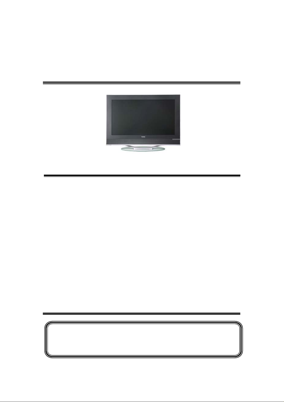
THOMSON
y
y
Service Manual
42M61NF21
1. Caution··························································································2
2. Specifications of chassis·································································6
3. Alignment Procedure······································································11
4. IC Brief Instruction·········································································19
5. Schematic Diagram········································································66
6. Block Diagram···············································································80
7. PCB Layout···················································································81
8. Explode View·················································································83
9. SpareParts····················································································89
This manual is the latest at the time of printing, and does not
include the modification which ma
the constant improvement of product.
be made after the printing, b
Page 2

CAUTION:
RISK OF ELECTRIC
SHOCK DO NOT OPEN.
1
Use of controls, adjustments or procedures other than those specified herein may result in
hazardous radiation exposure.
CAUTION: TO REDUCE THE RISK OF
CAUTION
The lighting flash with arrowhead symbol, with an equilateral triangle is intended to
alert the user to the presence of uninsulated voltage within the product s
enclosure that may be of sufficient magnitude to constitute a risk of electric shock to
the person.
The exclamation point within an equilateral triangle is intended to alert the user to the
presence of important operating and maintenance (servicing) instructions in the
literature accompanying the appliance.
ELECTRICAL SHOCK, DO NOT REMOVE
COVER (OR BACK). NO USER SERVICEABLE
PARTS INSIDE. REFER SER VICING TO
QUALIFIED SERVICE PERSONNEL.
dangerous
WARNING: TO REDUCE RISK OF FIRE OR ELECTRIC SHOCK, DO NOT
EXPOSE THIS APPLIANCE TO RAIN OR MOISTURE.
2
Page 3

IMPORTANT SAFETY INSTRUCTIONS
CAUTION:
Read all of these instructions. Save these instructions for later use . Follow all Warnings and
Instructions marked on the audio equipment.
1. Read Instructions-All the safety and operating instructions should be read before the product is operated.
2. Retain Instructions- The safety and operating instructions should be retained for future reference.
3. Heed Warnings- All warnings on the product and in the operating instructions should be adhered to.
4. Follow Instructions- All operating and use instructions should be followed.
FOR YOUR PERSONAL SAFETY
1. When the power cord or plug is damaged or frayed, unplug this television set from the wall outlet and refer servicing to
qualified service personnel.
2. Do not overload wall outlets and extension cords as this can result in fire or electric shock.
3. Do not allow anything to rest on or roll over the power cord, and do not place the TV where power cord is subject to
traffic or abuse. This may result in a shock or fire hazard.
4. Do not attempt to service this television set yourself as opening or removing covers may expose you to dangerous
voltage or other hazards. Refer all servicing to qualified service personnel.
5. Never push objects of any kind into this television set through cabinet slots as they may touch dangerous voltage
points or short out parts that could result in a fire or electric shock. Never spill liquid of any kind on the television set.
6. If the television set has been dropped or the cabinet has been damaged, unplug this television set from the wall outlet
and refer servicing to qualified service personnel.
7. If liquid has been spilled into the television set, unplug this television set from the wall outlet and refer servicing to
qualified service personnel.
8. Do not subject your television set to impact of any kind. Be particularly careful not to damage the picture tube surface.
9. Unplug this television set from the wall outlet before cleaning. Do not use liquid cleaners or aerosol cleaners. Use a
damp cloth for cleaning.
10.1. Do not place this television set on an unstable cart, stand, or table. The television set may fall, causing serious injury
to a child or an adult, and serious damage to the appliance. Use only with a cart or stand recommended by the
manufacturer, or sold with the television set. Wall or shelf mounting should follow the manufacturer s instructions, and
should use a mounting kit approved by the manufacturer.
10.2. An appliance and cart combination should be moved with care. Quick stops, excessive force, and uneven surfaces
may cause the appliance and cart combination to overturn.
3
Page 4
PROTECTION AND LOCATION OF YOUR SET
11. Do not use this television set near water ... for example, near a bathtub, washbowl, kitchen sink, or laundry tub, in a
wet basement, or near a swimming pool, etc.
Never expose the set to rain or water. If the set has been exposed to rain or water, unplug the set from the wall
outlet and refer servicing to qualified service personnel.
12. Choose a place where light (artificial or sunlight) does not shine directly on the screen.
13. Avoid dusty places, since piling up of dust inside TV chassis may cause failure of the set when high humidity persists.
14. The set has slots, or openings in the cabinet for ventilation purposes, to provide reliable operation of the receiver, to
protect it from overheating. These openings must not be blocked or covered.
Never cover the slots or openings with cloth or other material.
Never block the bottom ventilation slots of the set by placing it on a bed, sofa, rug, etc.
Never place the set near or over a radiator or heat register.
Never place the set in enclosure, unless proper ventilation is provided.
a built-in
PROTECTION AND LOCATION OF YOUR SET
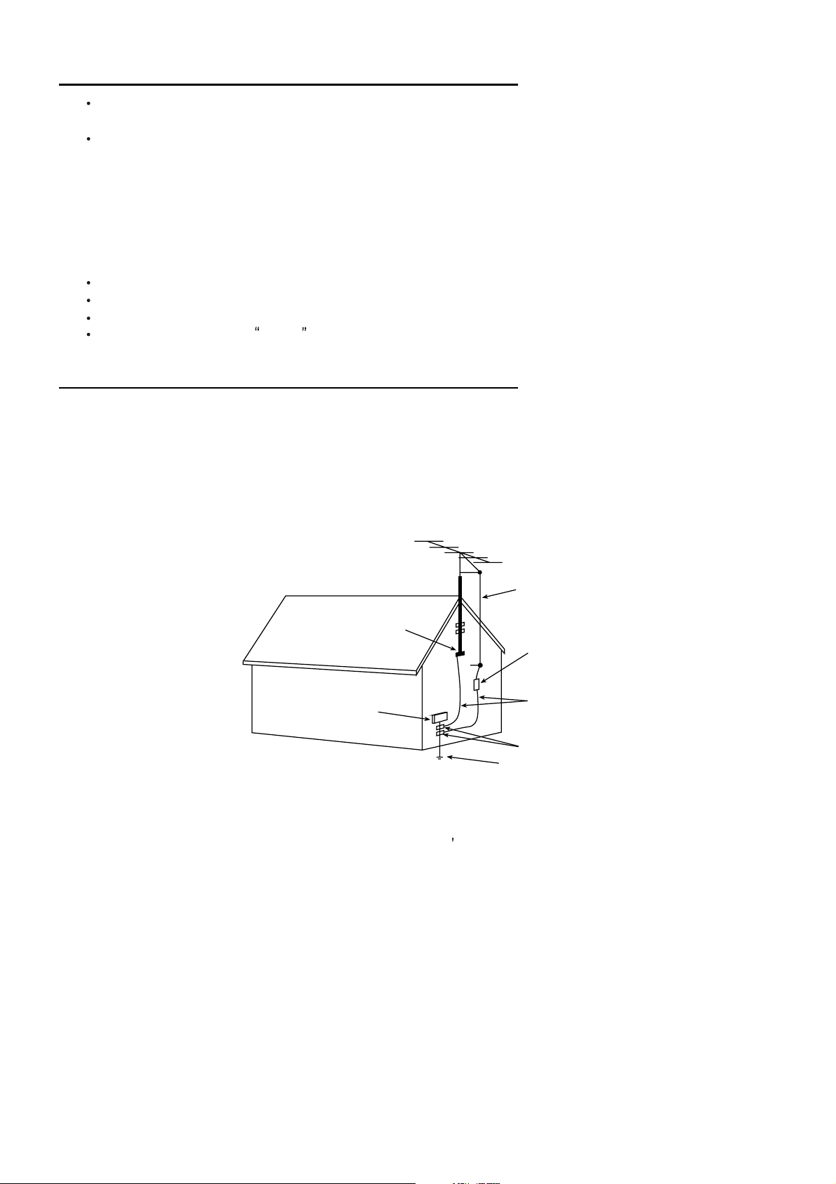
15.1. If an outside antenna is connected to the television set, be sure the antenna system is grounded so as to provide some
protection against voltage surges and built up static charges, Section 810 of the National Electrical Code, NFPA No.
70-1975, provides information with respect to proper grounding of the mast and supporting structure, grounding of the
lead-in wire to an antenna discharge unit, size of grounding conductors, location of antenna discharge unit, connection
to grounding electrode, and requirements for the grounding electrode.
EXAMPLE OF ANTENNA GROUNDING AS PER NATIONAL ELECTRICAL CODE INSTRUCTIONS
EXAMPLE OF ANTENNA GROUNDING AS PER
NATIONAL ELECTRICAL CODE
ANTENNA
LEAD- IN WIRE
GROUND CLAMP
ANTENNA DISCHARGE
UNIT (NEC SECTION
810-20)
GROUNDING
ELECTRIC SERVICE
EQUIPMENT
NEC-NATIONAL ELECTRICAL CODE
15.2. Note to CATV system installer : (Only for the television set with CATV reception)
This reminder is provided to call the CATV system attention to Article 820-40 of the NEC that provides
installer s
guidelines for proper grounding and, in particular, specifies that the cable ground shall be connected to the grounding
system of the building, as close to the point of cable entry as practical.
16. An outside antenna system should not be located in the vicinity of overhead power lines or other electric lights or power
circuits, or where it can fall into such power lines or circuits. When installing an outside antenna system, extreme care
should be taken to keep from touching such power lines or circuits as contact with them might be fatal.
CONDUCTORS
(NEC SECTION810-21)
GROUND CLAMPS
POWER SERVICE GROUNDING
ELECTRODE SYSTEM
(NEC ART 250. PART H)
17. For added protection for this television set during a lightning storm, or when it is left unattended and unused for long
periods of time, unplug it from the wall outlet and disconnect the antenna. This will prevent damage due to lightning
and power-line surges.
4
Page 5

OPERATION OF YOUR SET
18.
This television set should be operated only from the type of power source indicated on the marking label.If you are not
sure of the type of power supply at your home, consult your television dealer or local power company. For television
sets designed to operate from battery power, refer to the operating instructions.
19. If the television set does not operate normally by following the operating instructions, unplug this television set from the
wall outlet and refer servicing to qualified service personnel. Adjust only those controls that are covered in the operating
instructions as improper adjustment of other controls may result in damage and will often require extensive work by a
qualified technician to restore the television set to normal operation.
20. When going on a holiday : If your television set is to remain unused for a period of time, for instance, when you go on
a holiday, turn the television set and unplug the television set from the wall outlet.
off
IF THE SET DOES NOT OPERATE PROPERLY
21. If you are unable to restorenormal operation by followingthe detailed procedure in your operating instructions,
do not attempt any further adjustment. Unplug the set and call your dealer or service technician.
22. Whenever the television set is damaged or fails, or a distinct change in performance indicates a need for
service, unplug the set and have it checked by a professional service technician.
23. It is normal for some TV sets to make occasional snapping or popping sounds, particularly when being
turned on or off. If the snapping or popping is continuous or frequent, unplug the set and consult your
dealer or service technician.
FOR SERVICE AND MODIFICATION
24. Do not use attachments not recommended by the television set manufacturer as they may cause hazards.
25. When replacement parts are required, be sure the service technician has used replacement parts specified
by the manufacturer that have the same characteristics as the original part. Unauthorized substitutions
may result in fire, electric shock, or other hazards.
26. Upon completion of any service or repairs to the television set, ask the service technician to perform
routine safety checks to determine that the television is in safe operating condition.
5
Page 6
Specification
Item description
ID
Brand THOMSON
Panel technology (LCD / PDP) LCD
Display mode TFT LCD
Display Type TFT LCD
Category (Monitor/TV/…) TV
Market Position (Scenium/Intuiva/Mid/Access,,,) ACCESS
FG Supplier (TTE/External supplier) TTE
FG assy location (ZY/AN/HZ/External supplier) ZY
Cabinet Design (Example: SC VII, V 6,,,) M61
PJO Nb M61
General
EAN Code 3244480283943
Tocom code
Product number
Predecessor (replace) Chassis name MT02+DE200
Homologation (Gostandard/CE/MPTT/…) CE
MP date request by PC (ETA)
MP date confirmed by supplier (ETD/ETA)
Screen size : diagonale (inch) 42
Aspect ratio (16/9 // 4/3 // 15/9) 16/9
Color depth (8/10/12 bits) 8
1st panel supplier : panel suppliers 50 Hz progressive scan
1st panel supplier : panel reference LPL
1st panel supplier : resolution
1st panel supplier : pixel Pitch (mmxmm) 1920x1080
1st panel supplier : Horizontal and vertical viewing
angle
1st panel supplier : Typical response time (Grey to
Grey)
1st panel supplier : Typical response time (tr+tf) 8
1st panel supplier : Typical white luminance (Nits) 18
2.Prodcut Specification
Model(型号):LCD42M61NF21
LC420WU1-SLB1
0.1615x0.4845
178/178
Page 7
1st panel supplier : Contrast VESA std 550
e
1st panel supplier : Typical panel Life Time (Hours) 800:1
2st panel supplier : panel suppliers 60,000
Pictur
2st panel supplier : panel reference
2st panel supplier : resolution
2st panel supplier : pixel Pitch (mmxmm)
2st panel supplier : Horizontal and vertical viewing
angle
2st panel supplier : Typical response time (Grey to
Grey)
2st panel supplier : Typical response time (tr+tf)
2st panel supplier : Typical white luminance
(Nits)(1st source/2nd source)
2st panel supplier : Contrast VESA std(1st
source/2nd source)
2st panel supplier : Typical panel Life Time
(Hours)(1st source/2nd source)
Noise Reduction (adaptative/…) Yes
Comb Filter (2D/3D) 3D
Deinterlacer (no/linerar/motion adaptive/motion
compensative)
Film mode / reverse 3:2 pull down yes / yes
Format control (Pin8/WSS) Yes/Yes
16/9 autoformat (black bars canceller) no
Zoom type : 4/3 format Yes
Zoom type : 14/9 Zoom no
Zoom type : 16/9 Zoom Yes
Zoom type : 16/9 Zoom up/down No/No
VideoSound
Zoom type : Cinerama Yes
Zoom type : 16/9Format Yes
Colour preset (Cool/Normal/Warm/Favourite) Cool/Normal/Warm
Contrast expend (low/medium/high) high
Picture Reset on factory menu
Backlight Adjust on factory menu
Picture Autoadjustment (PC mode) Yes
Picture presets : Standard / Film / Studio / Sport /
Personal / Game / Video Camera
Music Power (Watt) 2*15W
RMS Power (Watt) 2*8W
Graphic Equalizer Yes
Treble, Bass, Balance, Volume, Mute Control -/-/ Yes/Yes/Yes
Sound presets (My
sound/Music/Film/Voice/Flat/Standard/Panorama)
Sound techno (Stereo Nicam/Virtual Dolby
Surround/SRS Trusurround XT/BBE Viva/SRS WoW
/…)
Loudspeakers built in (T/M/B) -/2/DPS/DPS+ Standard BG/DK/I/LL`
linerar/motion adaptive/motion
compensative
Standard / Film / Studio / Sport / Personal
normal/personal/rock/pop/live/dance/techn
o/classic/soft
NICAM,German Stereo,Virtual surround
Page 8
Color System (PAL/SECAM/NTSC) PAL/SECAM/NTSC(AV)
prog
)
g
DVBT (yes/no) Yes
Video standard NTSC 3.58 / 4.43 (AV) Yes
HD capability
Compatible video format if DVD/USB:
DviX/VCD/SVCD/JPEG/AVI/MPEG2/WMV- HD/SD
Compatible audio format if DVD/USB:
MP3/WMA/AAC/MPEG1/…
PC capability (up to maximum format) 1280*1024 60Hz
Playable Discs (CD/CD-R(RW)/CD-
Decoding capabilityUser convenience
ROM/DVD+R/+RW/-R/-RW)
Card reader format compatibility -
IB languages
DVD player (No/slot/tray) No
Program Numbers (example: 99+3AV) 99+1AV+2SCART
Number of buttons on cabinet (Power; Vol+/-; Pr+/-,
Menu )
Main switch button (yes/no) No
Clock Yes
Sleep timer Yes
wake-up timer Yes
Calendar / Games Yes/Parent Control - Channel lock (Input code for certain
channel)
Parent Control - Child lock (set the lock of the
keyboard, only the RCU can control the TV)
Parent Control - Kid pass (preset the ontime,
channel for each day of the week)
Parent Control - Channel lock (For digital
transmission and DVD program, to filter some
ramms
Program auto switch off No
OSD Language*
OSD Positioning No
OSD Transparency Adjust No
OSD Timeout Adjust No
Text Standard: (Top, FLOF,,,) TOP & FLOF
Teletext Level: 2.5 / 1.5 1.5
Pages for teletext 1000
Teletext character sets ****
TV Guide No
Auto Naming/Auto Sorting Yes/Yes
YES (720p, 1080i 50/60; 1080p 25/30;
480i/p; 576i/p)
-
-
–
DE, FR, IT, ES, EN, PL, CS, HU, RU, PT,
EL, NL, SV, DA, FI, NO
Power, PR +/–, Vol +/–, Menu
Yes
Yes
No
Yes
Germany、English、Netherlandish、
Italian、Finnish、Spanish、Danish、
French、Portuguese、Poland、
Norwe
Latin Pan-Euro West
Latin Pan-Euro East
Cyrillic West
Greek West
Arabic West
ian、Swedish、 Czechic
Page 9
Auto update (for DVBT software ugrades) No
Multipicture : PIP (Double Tuner) / PIP (AV) / PAP /
PAT / PIC
Hotel mode (Y/N) No
Tuner FM (yes/no) No
RF Input (Antenna): Analogical / Digital 1 /1
Scart 1 : CVBS / RGB / S-VIDEO 1/1/Scart 2 : CVBS / RGB / S-VIDEO 1/-/1
Scart 3 : CVBS / RGB / S-VIDEO -
only PAT
CINCH audio in / out (No volumpe control on Audio
out/can be jack 3,5mm)
CINCH video in / out 1(side)/S-video in / out -/Component Video Input (YCrCb/YPrPb) 1
Component Audio Input (YCrCb/YPrPb) Share with the VGA Audio input
VGA in / Audio L/R in / Jack audio in 3.5mm 1/1/HDMI 2
DVI-HDCP Share with HDMI
Audio input for DVI – HDCP Share with Audio VGA
CINCH subwoofer out / Coaxial out (SP-DIF) -/Headphone connector (mm) 1 (side)
RS232 (Y/N) Card Readers USB slot (NO/1.1/2) -
Connectors (if possible, please indicate the position)Accessories included
DVBC-I (common interface) yes
1(side)/1
External power converter Remote control reference RCT 311TV1G
Carton (English/French/Spanish) yes(English)
Batteries yes
IB yes
Product registration Card no
AC power cords yes
Audio Cord (Jack 3.5mm) no
VGA Cord no
Wallmount No
Antenna Cable no
Size (W x H x D, with stand) in mm 1058X765X270
Size (W x H x D, without stand) in mm 1058X711X116
Package Size (W x H x D, with stand) in mm 1214*364*889
Data
Page 10
Net Weight in kg 27.5
l
Gross Weight in Kg 33
Power supply 220V50Hz
Genera
Power consumption working / standby / Annual 240W/ 1W /Wallmount VESA compatible (standard reference) VESA compatible
Adaptor for VESA wallmount compatibility
(accessory ref)
Desktop Stand (included/optionnal + ref/NO) yes
Panel Tilt (Fowards/Backwards/Rotation) no
Swivel function desktop stand (yes/no) + motorized? no
Docking station (yes/no) no
Floor Stand (included/optionnal + ref/NO) no
Glass shield (yes/no) no
Finish on Front GES704S as moulded (high glossy black)
Finish on side RBK60TH(A8252) as moulded (black)
Finish on back RBK60TH(A8252) as moulded (black)
ID specification reference (file name) Graphic specification reference (file name) Finish on stand Transparent
number of colors on carton box 1
Brand logo Thomson Inlet
Other logo Full HD/DVB on front
Design / Mechanical
Screen Stikers External AC/DC Power with DC power cord (yes/no)
Handle (yes/no) no
Detachable speaker (yes/no) no
Number of Speaker 2
Rating Label langages
Rating Label Logos/Icons (GOST, Bin, Recycling,
Caution, …)
DE, FR, IT, ES, EN, PL, CS, HU, RU, PT,
no grounded plug
EL, NL, SV, DA, FI, NO
no
no
TBD
Page 11

LCDM61NF21(MT02+DE200) Factory Alignment Specification
ǃ
3.Alignment Procedure
General Description
LCD42/37M61NF21 is designed for Europe, using 37/42 inch Full HD
panel. The main chip is MTK8206. Support 1x RF in, 0.5x SCART, 1XSCART,
1xYPbPr, 1xVGA, 1xside AV include YC input, 2xHDMI,1x headphone out,
1xDVB-T input. The detail please refer the SyRS˅
1
Main board alignment
For Analog part
Before power on, please check and make sure the output of U20ˈU21ˈ
U22ˈU23,U24ˈU30ˈU31 are not shorted to grand.
Supply 5v to P504 and test the output of U20, the normal is 3.3V+/-5%, the
U21 output should be 1.8V+/-5%
Download the SW to the main chip, please see the chapter of how to
download
Check all the function of the all others board on the test tool
For PCMCIA interface
Digital module servicing and debug hints.
Mainly point:
1. Check PCB and each section power supply: 12V, 5V, 1.2V,1.8V ,3.3V.
2. Switch on the power, then measure the signal of output port of video and
audio.
If no output, check the following point:
1) video output of CPU section.
2) 4Mhz clock of the tuner output
3) Output of chip 74AHC1GU04( position U24 of schematic). 4Mhz clock
signal
to CUP(PNX8314).
4) Signal of SDRAM and flash chip when working .
5) Audio DAC ( component’s position U6 of schematic.
By contraries, enter the menu’s manual research item, and set appointed
channel number, check the signal indicator on TV screen.
3. Normal there is a signal level display on the menu.
If no displaying for the signal state indicated information, check the
following point:
1) 4Mhz clock signal of the tuner output,
2) Output of chip 74AHC1GU04(component’s position U23 of
schematic).
3) Else channel decoder schematic section.
4. When it display the signal state indicated information, Press “ok’ button,
and research program. It will not play the program if not get the program
Page 12
LCDM61NF21(MT02+DE200) Factory Alignment Specification
ǃ
list. Please check: components of the TS output from TDA10046 to CPU.
5. Inset the CAM card( PCMCIA CARD) to CI connector, the integrated
system will
detect it. if system has not found it, please check:
1) Input clock of Chip CIMAX SP2, The clock outputs from XD1
(component
XD1 of schematic) to chip CIMAX SP2.
2) Components and schematic of CI section ,
6. If not communication from ATV to digital module, Please check: I2C
of
the ATV( MT01 section) and digital module.
7. Check the SPDIF output. Connect SPDIF to Digital Power Amplifier.
Note: 4Mhz clock signal is sent out from tuner(TD1316A-MK3),
then distributed the clock to tda10046aht and pnx8314.
2
Final alignment
Fix mainboard on the test toolˈpower on ˈcheck and make sure all the port are
good
Source Test signal Test pattern Conclusion
Tuner Cable Full band Picture &
sound is ok
SCART1/2/SAV-C
VBS
SCART1/SAV-YC PM5418 PAL, half color &
SCART1/-RGB PM5418 PAL, half color &
PM5418 PAL, half color &
Gray bar
Gray bar
Gray bar
Picture &
sound is ok
Picture &
sound is ok
Picture &
sound is ok
SCART1 CVBS out cable First channel Picture &
sound is ok
HDMI DVD with HDMI
certification
VGA Chorma 2326 or
2327
Movie,720p
@60Hz
1024x768@60Hz
haft color & Gray
Picture &
sound is ok
Picture &
sound is ok
headphone Cable First channel sound is ok
Loud speaker Cable First channel Phase is
OK
YUV(YPbPr) chroma2327/BSG-3
60A/DVD
1080i@60Hz
haft color & Gray
Picture &
sound is ok
3ǃThe way to Factory menu
Page 13

LCDM61NF21(MT02+DE200) Factory Alignment Specification
˖
˅ˊ
Enter the factory menu (can use the IR and press the remote key “vol-”to
“0’, press mute remote key ,then press 9,7,3,5 remote key. Press right key
to
enter the sub-menu and press MENU key to return the main-menu
4ǃBalance Adjust
Adjust the temperature in CMP, VGA, AV. Please make sure the picture
mode is set to “Stand”, the “PictureÆ Black expand” on the user Menu is set to
“OFF”. “OtherÆFlesh Tone & Adaptive Luma Control ” on the factory Menu is
set to “OFF”. After Alignment, all the item will change to “ON”
ADC Adjust
A. For CMP input, the test signal is 576i/50Hz, 100%, 8 steps colour bar.
Select the “BalanceÆRGB Calibrate” on the factory Menu, then press ”Æ”.,
ADC adjust is finished after “OK” is displayed
B. For VGA input, the test signal is 1024h768/60Hzˈwhite/black grid.
Select the “BalanceÆRGB Calibrate” on the factory Menu, then press ”Æ”.,
ADC adjust is finished after “OK” is displayed
1
VGA :
For VGA input, the test signal is 1024h768/60Hzˈ16 steps gray bar. Set
the “BalanceÆ Tone” on factory menu to “Normal”:
AǃFor the third step form the white bar, Adjust the value of White RǃWhite
GǃWhite B, until the color temperature is x=280f5ˈy=290f5ˈY > 220nit
BǃFor the second step form the black bar, Adjust the value of Gray Rǃ
Gray GǃGray B, until the color temperature is x=280f5ˈy=290f5ˈY < 25nit
Cǃrepeat A&B, until all is ok
DǃAdjust the value of Black level
2˅ˊAV
For AV3 input, the test signal is PALˈ8 steps gray bar. Set the “BalanceÆ
Tone” on factory menu to “Normal”:
AǃFor the third step form the white bar, Adjust the value of White RǃWhite
GǃWhite B, until the color temperature is x=280f5ˈy=290f5ˈY > 220nit
BǃFor the second step form the black bar, Adjust the value of Gray Rǃ
Gray GǃGray B, until the color temperature is x=280f5ˈy=290f5ˈY < 25nit
Cǃrepeat A&B, until all is ok
DǃAdjust the value of Black level
3˅ˊCMP
For CMP input, the test signal is 576i/50Hzˈ16 steps gray bar. Set the
“BalanceÆ
Tone” on factory menu to “Normal”:
Page 14
LCDM61NF21(MT02+DE200) Factory Alignment Specification
AǃFor the third step form the white bar, Adjust the value of White RǃWhite
GǃWhite B, until the color temperature is x=280f5ˈy=290f5ˈY > 220nit
BǃFor the second step form the black bar, Adjust the value of Gray Rǃ
Gray GǃGray B, until the color temperature is x=280f5ˈy=290f5ˈY < 25nit
Cǃrepeat A&B, until all is ok
DǃAdjust the value of Black level
4). Adjust the value of Black level
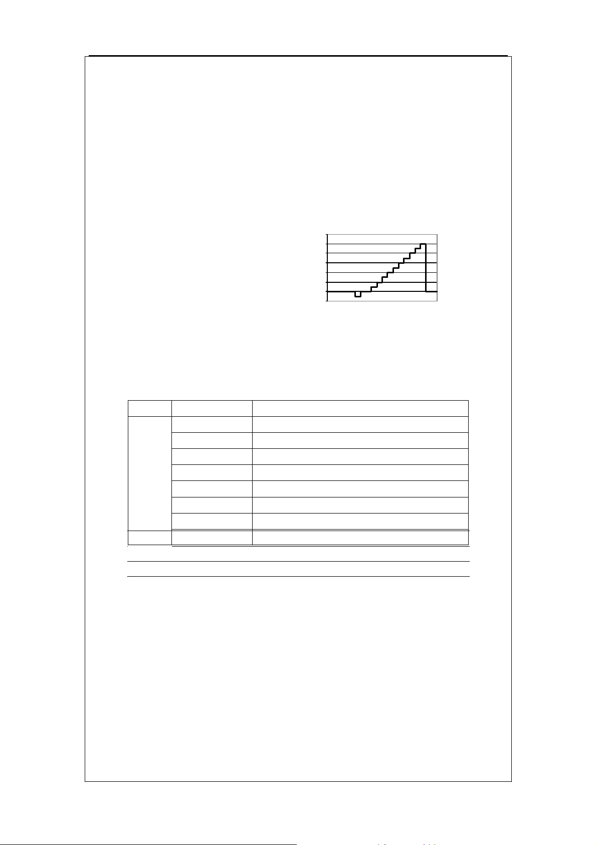
Measurements are using ‘SCALBRI2.UPA’ patterns with -1% to 10% video
level bars.
12%
10%
8%
6%
4%
2%
video level (%)
0%
-2%
time
Basic video signal is following:
Change the Black level to make sure the value is 0-3%.
5ǃFactory Menu definition˖
1˅ˊ System
Item Sub-item
Power Mode Remember˖Remember the state of
Factory Key OFF˖Factory Key is invalidation
Tuner AGC 12
Key Board On˖the keypad board is locked, only
LOGO Select the POWER ON LOGO
Pattern Come from IC MT8201. It is used for
Back Light Peak White Alignment
Reset Reset EEPROM data, and load the
2)ˊ Balance
Page 15
LCDM61NF21(MT02+DE200) Factory Alignment Specification
Source For balance source
Balan
ce
Tone Normal/Warm/Cool White R R White balance
White G G White balance
White B B White balance
Gray R R Gray balance
Gray G G Gray balance
Gray B B Gray balance
RGB
ADC adjust
Calibrate
Black Level
3)ˊTV Geometry
Item Sub-item
TV Geo
Color System
H POS Horizontal Position
H SIZE Horizontal Size
V POS Vertical Position
V SIZE Vertical Size
Scaling Brightness User Menu’s Brightness
Scaling Contrast User Menu’s Contrast
Scaling Colour User Menu’s Colour
Scaling Hue User Menu’s Hue
4)ˊNicam All of item are for Debug, Don’t modify!
Item Sub-item
Nicam
Correct
5
Thres
Sync Loop 50
Error Thre 6
ParityErrorT
47
hres
EveryNumFr
32
ames
5)ˊMono All of item are for Debug, Don’t modify!
Item Sub-item
High DEVI OFF
AM Mute ON
AM Mute
69
High
AM Mute
53
Low
Carrier Shift OFF
Saturation
OFF
Mute
FM mute ON
Page 16
LCDM61NF21(MT02+DE200) Factory Alignment Specification
FM mute
24
High
FM mute
19
Low
6)ˊSound Volume Curve
Item Sub-item
Soun
d
VOL_0 0
VOL_10 1
VOL_50 60
VOL_90 204
VOL_100 254
TV Pre TV pre- amplify
AV Pre TV pre- amplify
SWPREQ For debug
7)ˊOther乍 All of item are for Debug, Don’t modify!
Item Sub-item
Other
Blue Mute ON
CTI Middle
Flesh Tone Switch to “OFF” during alignment and
CAL Measurement.
Swtich to “ON” for Out of Box Settings
Adap
Luma….
Switch to “OFF” during alignment and
CAL Measurement.
Swtich to “ON” for Out of Box Settings
Deinter
Automatic
Mode
WhitePeak
limitor
Switch to “OFF” during alignment and
CAL Measurement.
Swtich to “ON” for Out of Box Settings
MDDi Edge
High
Pre
TTX
10
Contrast
Seamless Off
8)ˊINFO SW version information
Info
Project LCD32MT01M1
Version XXXXXX
Date 2007-1-5
Page 17
LCDM61NF21(MT02+DE200) Factory Alignment Specification
˖
6ǃFactory default settings
Source TV(channel 1)
Picture Preset Standard
Black expand ON
Tone Normal
USE
R
MEN
U
Noise reduction Low
Volume 30
Sound type Automatic
Virtual Surrond OFF
Auto Volume OFF
Sound effect OFF
FACTTORY-KEY OFF
FACT
TOR
Y
MEN
POWER ON OFF
Flesh Tone ON
Adaptive Luma
Control.
U
ON
7ˊAnalog board software update
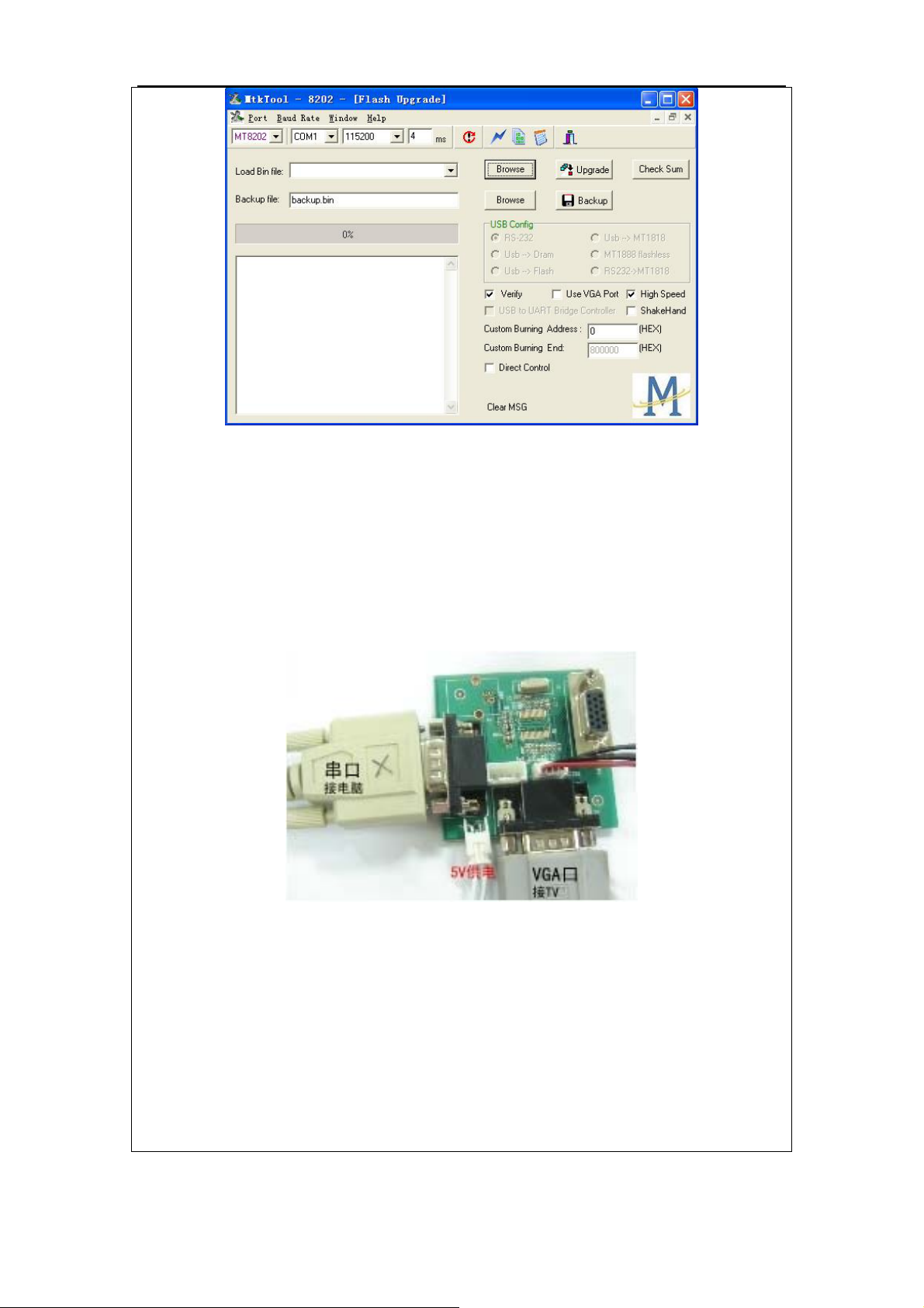
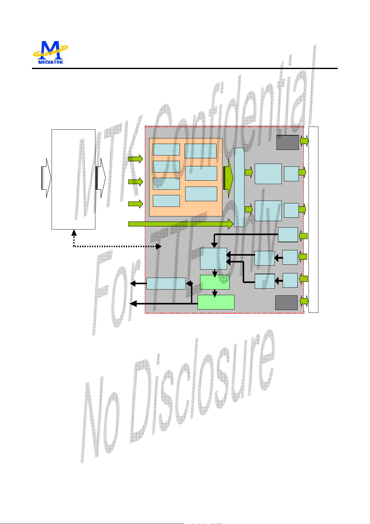
Solution 1˖
Prepare MTKTOOL UPDATE, update board, serial line.
(1)ǃConnect PC, update board, and J3 on the main board with serial line
(2)ǃProvide the STB +5V for main board
(3)ǃOpen “MtkTool.exe” in MTK TOOL program, and set the parameter as
below picture
Page 18
LCDM61NF21(MT02+DE200) Factory Alignment Specification
(4)ǃPress “Browse” for selecting the SW.
(5)ǃPress “Upgrade” to download the SW. It will be OK when it show “100%”
(6)ǃAfter downloading SW, it will be long time for Initializing EEPROM.
Solution 2˖
Preparative is same with above.
Set SYSTEM->FactoryKey on factory MENU to OFF. Connect the device
as below picture.
Update the SW follow solution1- (3), (4), (5), (6)
Page 19

4.IC Brief Instruction
DOCUMENT ARE SUBJECT TO CHANGE WITHOUT NOTICE MTK CONFIDENTIAL, NO DISCLOSURE
MT8206
1. Features description
MT8206
format up to HDTV. It includes 3D comb filter TV decoder to retrieve the best image from
popular composite signals. Embedded HDTV/VGA decoders enable the high quality video
reproduction. 24/16/8 bits digital port may accept all kinds of external digital input video source.
New 3
video into progressive non-flicking video. 2D Graphic engine generates high quality UI
interface. Advanced full function color processing with fully 10-bit path provides high quality
video contents. Independent two Flexible scalars provide wide adoption to various LCD panels
for two of different video sources at the same time. Its on-chip audio processor decodes
analog signals from tuner with lip sync control, delivering high quality post-processed sound
effect to customers. On-chip microprocessor reduces the system BOM and shortens the
schedule of UI design by high level C program. MT8206 is a cost-effective and high
performance HDTV-ready solution to LCD TV product.
is a highly integrated single chip for LCD TV supporting video input and output
rd
generation advanced motion adaptive de-interlacer converts accordingly the interlace
FEATURE List
Analog front end
1 set of high resolution ADC with corresponding PGAs adopting to 0.5V~2V input dedicated for TV/AV/SV input signals
3 high speed ADCs dedicated for VGA/HDTV input signals up to 160MHz
All 8-bit programmable gain pre-amplifiers
Embedded Schmitt trigger and deglitch circuits on Hsync/Vsync/SOG/SOY inputs
Video Input
Embedded input Multiplexers without external switch including
10 for TV/AV/S-video input pins available for any possible combination
3 sets for VGA/Component/Scart/D-connector with differential input pairs
1 24/16/8 bit digital port for ITU601/656/RGB video format
1 additional 8 bit digital port for ITU656 video format
All the input sources can be flexibly routed to Main/PIP internally
Sync Processor
Two enhance sync processors for all timing detection supporting Macrovision detection
Enhanced measuring mechanism for VGA auto adjustment
Decoder
TVD
Single 3
Automatic TV standard detection supporting NTSC, NTSC-4.43, PAL (B, G, D, H, M, N, I, Nc), PAL (Nc), PAL, SECAM
Enhanced 3
rd
generation TV decoder
rd
generation NTSC/PAL Motion Adaptive 3D comb filter
June, 2006
Page 20

DOCUMENT ARE SUBJECT TO CHANGE WITHOUT NOTICE MTK CONFIDENTIAL, NO DISCLOSURE
Embedded VBI decoder for Closed-Caption/XDS/ Teletext/WSS/VPS
Supporting Macro vision detection
YPbPr/Scart/D-connector
Supporting HDTV 480i/480p/576i/576p/720p/1080i input
Smart detection on Scart function for European region
Smart detection on D-connector for Japan region
Supporting SCART RGB inputs mixed with composite signal by adjustable horizontal delay
VGA
Supporting various VGA input timings up to SXGA (1280x1024@75Hz).
Supporting Separate/Composite/SOG sync types
Digital port
1 digital port supporting DVI 24-bit RGB or CCIR-656/601 digital video input format
1 additional 8 bit digital port for ITU656 video format
VBI
Dual VBI decoders for the application of V-Chip/Closed-Caption/XDS/ Teletext/WSS/VPS
Supporting external VBI decoder by YPbPr input
VBI decoder up to 1000 pages Teletext.
Video Processor
Noise Reduction
All Video input source with motion adaptive 3D noise reduction
Color Management
Fully 10-bit processing to enhance the video quality
Advanced flesh tone and multiple-color enhancement. (For skin, sky, and grass…)
Gamma/anti-Gamma correction
Advanced Color Transient Improvement (CTI)
Saturation/hue adjustment
Contrast/Brightness/Sharpness Management
Sharpness and DLTI/DCTI
Brightness and contrast adjustment
Black level extender
Adaptive Luma/Chroma management
De-interlacing
rd
3
generation advanced Motion adaptive de-interlacing
Automatic detect film or video source
3:2/2:2 pull down source detection
Main/PIP 2 independent de-interlacing processor
Scaling
rd
3
generation high resolution arbitrary ratio vertical/horizontal scaling of video, from 1/32X to 32X
Advanced linear and non-linear Panorama scaling.
Picture-in-Picture (PIP)
Picture-Out-Picture (POP)
Display
Advanced dithering processing for LCD display with 6/8/10 bit output
10bit gamma correction
Supporting alpha blending for Video and two OSD planes
Frame rate conversion
Seamless performance comparing demonstration function
MT8206
June, 2006
Page 21

DOCUMENT ARE SUBJECT TO CHANGE WITHOUT NOTICE MTK CONFIDENTIAL, NO DISCLOSURE
Support Left/Right video processing comparing function without additional resources (DRAM…) for customers’
demonstration
All the video functions (De-interlace/3D comb/NR/Flesh tone/CTI) can be included
Video Output
Programmable output timing for 1080p panel.
Dual-channel 6/8-bit LVDS, single channel 6/8/10-bit LVDS
Supporting video output mirror and upside down
1 CVBS bypass output of CVBS/S-video(mixed) input
Audio Features
Supporting BTSC/EIAJ/A2/NICAM decode
Stereo demodulation, SAP demodulation
Mode selection (Main/SAP/Stereo)
Equalizer
Sub-woofer/Bass enhancement
MTK proprietary 3D surround processing (Virtual surround)
Audio and video lip synchronization
Supporting Reverberation
MT8206
Audio Input/Output
Decode audio AF from Tuner
1 set of audio L/R digital line in (MT8206 is Master)
7.1-channel slave digital line in
Supporting total 12-channels including full 7.1-channels digital output, 2- channel bypass and 2-channel headphone
output.
Embedded 3 internal audio DACs
Supporting 1 Tuner audio decoder and 1 digital input and both output for SCART1/2 output application
2D-Graphic/OSD processor
Embedded two backend RGB domain OSD planes and one YUV domain OSD plane. To support Main/PIP
Teletext/Close-caption functions together with setup menu
Supporting alpha blending among these two planes and video
Supporting Text/Bitmap decoder
Supporting line/rectangle/gradient fill
Supporting bitblt
Supporting color Key function
Supporting Clip Mask
65535/256/16/4/2-color bitmap format OSD,
Automatic vertical scrolling of OSD image
Supporting OSD mirror and upside down
Host Micro controller
Turbo 8032 micro controller
Built-in internal 373 and 8-bit programmable lower address port
2048-bytes on-chip RAM
June, 2006
Page 22

DOCUMENT ARE SUBJECT TO CHANGE WITHOUT NOTICE MTK CONFIDENTIAL, NO DISCLOSURE
Up to 4M bytes FLASH-programming interface
Supporting 5/3.3-Volt. FLASH interface
Supporting power-down mode
Supporting additional serial interface
IR control serial input
Supporting 2 RS232 interface for external source communication
Supporting single interface directly supporting SD/MS/MMC memory card
Supporting 2 PWM output
Programmable GPIO setting for complex external device control
DRAM Controller
Supporting up to 32M-byte SDR/DDR DRAM
Supporting 2x16 bit SDR/DDR bus interfaces
Build in a DRAM interface programmable clock to optimize the DRAM performance
Programmable DRAM access cycle and refresh cycle timings
Supporting 3.3/2.5-Volt SDR/DDR Interface
DRAM Usage
For features of 8206, Dual 8Mx16 DDR are used.
It is recommended to use dual 8Mx16 DDR (32MB) for following basic features.
MT8206
Function Full Screen PIP/POP
3D-Comb Y
MDDi Up to 1080i MDDi
Scale mode Normal/Full Normal/Full
VGA timing Up to
1280x1024@75Hz
Panel 1080P
z For PIP/POP mode, 1280x1024 should be under 60Hz.
z Case lists are evaluated when Dram clock = 169 MHz,DDRx2.
Flash Usage
Flash is used to store FW code, fonts, bitmaps, big tables for VGA, Video, Gamma..
In our demo system, we can support 2-4 languages within 1MB flash.
For single country, we need around 20KB to store font data.
For more bitmaps, we need more flash space to store them.
When POP mode, Main=AV, Sub=1080I, only one of HD MDDi and Comb
can be enable.
(for POP)Case i: Main=AV(with 3D Comb), Sub=1080i(Bob mode)
(for POP)Case ii: Main=1080i(Bob mode), Sub=AV(with 3D Comb)
(for POP)Case iii: Main=AV(without 3D Comb), Sub=1080i(HD MDDi)
(for POP)Case iv: Main=1080i(HD MDDi), Sub= AV(without 3D Comb)
When PIP mode, there is no constraint in 3D-Comb and MDDi.
Up to 1280x1024x60Hz
2Mbytes is recommended to build a general TV model.
Outline
June, 2006
Page 23

DOCUMENT ARE SUBJECT TO CHANGE WITHOUT NOTICE MTK CONFIDENTIAL, NO DISCLOSURE
388-pin BGA package
3.3/2.5V/1.8-Volt. operating voltages
0.18um process
MT8206
June, 2006
Page 24
PRELIMINARY, SUBJECT TO CHANGE WITHOUT NOTICE MTK CONFIDENTIAL, NO DISCLOSURE
MT8206
3. BLOCK DIAGRAM
CVBS / SV
(x8)
(Customer)
External
YPbPr
(x2)
Switches
VGA
Digital
Control Signal (GPIO, …)
LVDS
DAC
Analog Front End
ADC
ADC
3D TVD
HDTVD
ADC
VGAD
ADC
Digital Path
LVDS Tx
Gamma
Dithering
Merge
MUX
8032
Main Path
MDDi
PIP Path
MDDi
OSD
Color
Color
DSP
DS
DRAM
DS
US
US
June, 2006
Page 25

PRELIMINARY, SUBJECT TO CHANGE WITHOUT NOTICE MTK CONFIDENTIAL, NO DISCLOSURE
MT8206
4. MT8206 PIN DESCRIPTION
4.1GENERAL PIN LIST:
Item Symbol Pin # Type Description
DIGITAL
Power/Ground (41)
1 DVDD33A D5, H4 I 3.3V power (necessary when power saving)
2 DVDD33 AA4, AC17, AC20 I 3.3V power for all the 3.3V I/O pins
2 DVSS33 L11, N12, R15, T16 I 3.3V ground
3 DVDD25 AC5, AC6, AC7, AD5, AD6, I 2.5V power for DDR (for 16/32 bit DDR)
DVDD25OPT AC14, AC15, AD15 I 2.5V power for DDR (for 32 bit DDR), 3.3V power for GPIO
DVSS25 N11, P11, R11, T11, R13,
T13, T14
5 DVDD18A K3, K4 I 1.8 V power (necessary when power saving)
DVDD18 U3, U4, AC8, AC9, AC22,
AC23
6 DVSS18 L12, M11, M12, P12, R12,
R14, R16, T12, T15
I 2.5V ground for DDR (for 16/32 bit DDR)
I 1.8 V power for internal digital part
I 1.8 V ground
RS232 (2)
1 RXD M3 I RS232 received data, 2mA
2 TXD M4 O RS232 transmitted data, 2mA
Serial interface (6)
1 SCL AA2 O
2 SDA AA1 I/O
3 SCL0 U23 I/O
4 SDA0 V23 I/O
5 SCL1 AB24 I/O
6 SDA1 AB23 I/O
Digital Audio Interface (8)
1) GPIO, 2mA
2) Clock of master serial interface, 2mA
1) GPIO, 2mA
2) Data of master serial interface, 2mA
1) Clock of slave0 serial interface, 2mA
2) GPIO
3) RS232 RXD
1) Data of slave0 serial interface, 2mA
2) GPIO
3) RS232 TXD
1) Clock of slave1 serial interface, 2mA
2) GPIO
1) Data of slave1 serial interface, 2mA
2) GPIO
1 AOMCLK M1 O Audio out master clock, 2~16mA, SR(optional), SMT
2 AOLRCK N3 O Audio out left-right clock, 4mA, SR, SMT
June, 2006
Page 26

PRELIMINARY, SUBJECT TO CHANGE WITHOUT NOTICE MTK CONFIDENTIAL, NO DISCLOSURE
Item Symbol Pin # Type Description
3 AOBCK N1 O Audio out bit clock, 2~16mA, SR(optional), PD(optional), SMT
MT8206
4 AOSDATA0 P1 O
5 AOSDATA1 P2 O
6 AOSDATA2 P3 O
7 AOSDATA3 P4 O
8 LIN N4 I Audio line in
Microcontroller and Flash Interface (38)
1 HIGHA0 G2 I/O
2 HIGHA1 F3 I/O
3 HIGHA2 F4 I/O
4 HIGHA3 E1 I/O
5 HIGHA4 E2 I/O
6 HIGHA5 E3 I/O
7 HIGHA6 E4 I/O
8 HIGHA7 D1 I/O
9 AD7 C4 I/O
10 AD6 B1 I/O
11 AD5 B2 I/O
12 AD4 A2 I/O
13 AD3 B3 I/O
14 AD2 A3 I/O
15 AD1 B4 I/O
1) GPIO (default, input in initial state)
2) Audio out data line 0, 4mA, SR, PD(optional), SMT
1) GPIO (default, input in initial state)
2) Audio out data line 1, 4mA, SR, PD(optional), SMT
1) GPIO (default, input in initial state)
2) Audio out data line 2, 4mA, SR, PD(optional), SMT
1) GPIO (default, input in initial state)
2) Audio out data line 3, 4mA, SR, PD(optional), SMT
Microcontroller address 8, 2~16 mA, PU, works in stand-by
mode
Microcontroller address 9, 2~16 mA, PU, works in stand-by
mode
Microcontroller address 10, 2~16 mA, PU, works in stand-by
mode
Microcontroller address 11, 2~16 mA, PU, works in stand-by
mode
Microcontroller address 12, 2~16 mA, PU, works in stand-by
mode
Microcontroller address 13, 2~16 mA, PU, works in stand-by
mode
Microcontroller address 14, 2~16 mA, PU, works in stand-by
mode
Microcontroller address 15, 2~16 mA, PU, works in stand-by
mode
Microcontroller address/data 7, 2~16 mA, SR, works in
stand-by mode
Microcontroller address/data 6, 2~16 mA, SR, works in
stand-by mode
Microcontroller address/data 5, 2~16 mA, SR, works in
stand-by mode
Microcontroller address/data 4, 2~16 mA, SR, works in
stand-by mode
Microcontroller address/data 3, 2~16 mA, SR, works in
stand-by mode
Microcontroller address/data 2, 2~16 mA, SR, works in
stand-by mode
Microcontroller address/data 1, 2~16 mA, SR, works in
stand-by mode
16 AD0 A4 I/O
17 IOA0 C2 I/O
18 IOA1 C1 I/O
June, 2006
Microcontroller address/data 0, 2~16 mA, SR, works in
stand-by mode
Microcontroller address 0 / IO, 2mA, SR, PU, works in
stand-by mode
Microcontroller address 1 / IO, 2mA, SR, PU, works in
stand-by mode
Page 27

Æ
Æ
PRELIMINARY, SUBJECT TO CHANGE WITHOUT NOTICE MTK CONFIDENTIAL, NO DISCLOSURE
Item Symbol Pin # Type Description
19 IOA2 D4 I/O
20 IOA3 D3 I/O
21 IOA4 G1 I/O
22 IOA5 H3 I/O
23 IOA6 H2 I/O
24 IOA7 H1 I/O
25 A16 D2 I/O
26 A17 C3 I/O
27 IOA18 G3 I/O
28 IOA19 G4 I/O
29 IOA20 F2 I/O
30 IOA21 F1 I/O
31 IOALE J1 I/O
32 IOOE# B5 I/O
33 IOWR# J2 I/O
34 IOCS# A5 I/O
35 UWR# K1 I/O
36 URD# K2 I/O
37 UP3_4 L3 I/O
38 INT0# L1 I/O
DIGITAL MISC (5)
1 PRST_ L2 I
Microcontroller address 2 / IO, 2mA, SR, PU, works in
stand-by mode
Microcontroller address 3 / IO, 2mA, SR, PU, works in
stand-by mode
Microcontroller address 4 / IO, 2mA, SR, PU, works in
stand-by mode
Microcontroller address 5 / IO, 2mA, SR, PU, works in
stand-by mode
Microcontroller address 6 / IO, 2mA, SR, PU, works in
stand-by mode
Microcontroller address 7 / IO, 2mA, SR, PU, works in
stand-by mode
2mA, PU, works in stand-by mode
1) Flash address 16
2) GPIO
2mA, PU, works in stand-by mode
1) Flash address 17
2) GPIO
2mA, SR, PD, SMT, works in stand-by mode
1) Flash address 18 / IO
2) GPIO
2mA, SR, PD, SMT, works in stand-by mode
1) Flash address 19 / IO
2) GPIO
2mA, SR, PD, SMT, works in stand-by mode
1) Flash address 20 / IO
2) GPIO
The GPIO function can work in the standby mode
2mA, SR, PD, SMT, works in stand-by mode
1) Flash address 21 / IO, While External FLASH size <=
2MB
2) GPIO
The GPIO function can work in the standby mode
Microcontroller address latch enable, 2mA, PU, SMT, works
in stand-by mode
Flash output enable, active low / IO, 2mA, SR, PU, SMT,
works in stand-by mode
2mA, PU, SMT, works in stand-by mode
1) Flash write enable, active low / IO
2) GPIO
SmA, SR, SMT, works in stand-by mode
1) Flash chip select, active low / IO
2) GPIO
Microcontroller write strobe, active low, 2mA, PU, SMT, works
in stand-by mode
Microcontroller read strobe, active low, 2mA, PU, SMT, works
in stand-by mode
Microcontroller port 3-4, 2mA, PU, SMT, works in stand-by
mode
Microcontroller external interrupt 0, active low, 2mA, PU,
SMT, works in stand-by mode
power on reset
, works in stand-by mode
MT8206
2 ICE M2 I
June, 2006
ICE mode
, works in stand-by mode
Page 28

PRELIMINARY, SUBJECT TO CHANGE WITHOUT NOTICE MTK CONFIDENTIAL, NO DISCLOSURE
MT8206
Item Symbol Pin # Type Description
3 PWM0 AD17 I/O
1) GPIO (default, input in initial state), 2mA
2) PWM output 0, 2mA
4 PWM1 AC18 I/O
1) GPIO (default, input in initial state), 2mA
2) PWM output 1, 2mA
5 IR L4 I/O
IR control signal input, 4mA, SR, SMT, works in stand-by
mode
GPIO (23)
1 GPIO0 R1 I/O
2 GPIO1 R2 I/O
(1) GPIO, 2~16mA, SR, SMT
(2) ASDATA4, ch9 and ch10 audio output
(1) GPIO, 2~16mA, SR, SMT
(2) ASDATA5, ch11 and ch12 audio output
3 GPIO2 R3 I/O GPIO, 2~16mA, SR, SMT
4 GPIO3 R4 I/O GPIO, 2~16mA, SR, SMT
5 GPIO4 T4 I/O GPIO, 2~16mA, SR, SMT
6 GPIO5 U1 I/O
7 GPIO6 U2 I/O
8 GPIO7 V1 I/O
9 GPIO8 V2 I/O
10 GPIO9 V3 I/O
(1) GPIO, 2~16mA, SR, SMT
(2) TXD of the 2
(1) GPIO, 2~16mA, SR, SMT
(2) RXD of the 2
GPIO, 2~16mA, SR, SMT
-> Add function: 2
GPIO, 2~16mA, SR, SMT
-> Add function: 2
GPIO, 2~16mA, SR, SMT
-> Add function: 2
nd
RS232 port
nd
RS232 port
nd
digital audio LRCK output
nd
digital audio AOBCK output
nd
digital audio AOMCLK output
11 GPIO10 V4 I/O GPIO, 2~16mA, SR, SMT
12 GPIO11 W1 I/O GPIO, 2~16mA, SR, SMT
13 GPIO12 W2 I/O GPIO, 2~16mA, SR, SMT
14 GPIO13 W3 I/O GPIO, 2~16mA, SR, SMT
15 GPIO14 W4 I/O GPIO, 2~16mA, SR, SMT
16 GPIO15 Y1 I/O GPIO, 2~16mA, SR, SMT
17 GPIO16 Y2 I/O GPIO, 2~16mA, SR, SMT
18 GPIO17 Y3 I/O GPIO, 2~16mA, SR, SMT
19 GPIO18 Y4 I/O GPIO, 2~16mA, SR, SMT
2mA, works in stand-by mode
20 GPIO19 D7 I/O
1) GPIO (default, input in initial state)
2) Monitored pin
2mA, works in stand-by mode
21 UP3_0 A7 I/O
1) GPIO (default, input in initial state)
2) UP30
June, 2006
Page 29

PRELIMINARY, SUBJECT TO CHANGE WITHOUT NOTICE MTK CONFIDENTIAL, NO DISCLOSURE
Item Symbol Pin # Type Description
3) Monitored pin
2mA, works in stand-by mode
22 UP3_1 B7 I/O
23 UP3_5 C7 I/O
1 FCIDAT T3 I/O
2 FCICLK T1 O
3 FCICMD T2 I/O
Dram Interface (60)
1) GPIO (default, input in initial state)
2) UP31
3) Monitored pin
2mA, works in stand-by mode
1) GPIO (default, input in initial state)
2) UP35
3) Monitored pin
FCI Interface (3)
2~16mA, SR, PU(optional), PD(optional)
1) GPIO (default, input in initial state)
2) SDIO in ms mode or DAT0 in SD mode
2~16mA, SR
1) GPIO (default, input in initial state)
2) MSCLK in ms mode or SDCLK in SD mode
2~16mA, SR, PU(optional), PD(optional)
1) GPIO (default, input in initial state)
2) BS in ms mode or CMD in SD mode
MT8206
1 DQ0 AB1 I/O dram data bus bit 0
2 DQ1 AB2 I/O dram data bus bit 1
3 DQ2 AB3 I/O dram data bus bit 2
4 DQ3 AB4 I/O dram data bus bit 3
5 DQ4 AC1 I/O dram data bus bit 4
6 DQ5 AC2 I/O dram data bus bit 5
7 DQ6 AC3 I/O dram data bus bit 6
8 DQ7 AC4 I/O dram data bus bit 7
9 DQ8 AF1 I/O dram data bus bit 8
10 DQ9 AE2 I/O dram data bus bit 9
11 DQ10 AF2 I/O dram data bus bit 10
12 DQ11 AE3 I/O dram data bus bit 11
13 DQ12 AF3 I/O dram data bus bit 12
14 DQ13 AD4 I/O dram data bus bit 13
June, 2006
Page 30

PRELIMINARY, SUBJECT TO CHANGE WITHOUT NOTICE MTK CONFIDENTIAL, NO DISCLOSURE
Item Symbol Pin # Type Description
15 DQ14 AE4 I/O dram data bus bit 14
16 DQ15 AF4 I/O dram data bus bit 15
17 DQ16 AC12 I/O dram data bus bit 16
18 DQ17 AD12 I/O dram data bus bit 17
19 DQ18 AE12 I/O dram data bus bit 18
20 DQ19 AF12 I/O dram data bus bit 19
21 DQ20 AC13 I/O dram data bus bit 20
22 DQ21 AD13 I/O dram data bus bit 21
23 DQ22 AE13 I/O dram data bus bit 22
24 DQ23 AF13 I/O dram data bus bit 23
25 DQ24 AD14 I/O dram data bus bit 24
MT8206
26 DQ25 AE15 I/O dram data bus bit 25
27 DQ26 AF16 I/O dram data bus bit 26
28 DQ27 AE16 I/O dram data bus bit 27
29 DQ28 AD16 I/O dram data bus bit 28
30 DQ29 AC16 I/O dram data bus bit 29
31 DQ30 AF17 I/O dram data bus bit 30
32 DQ31 AE17 I/O dram data bus bit 31
33 RA0 AD8 O dram address bus bit 0
34 RA1 AE8 O dram address bus bit 1
35 RA2 AF8 O dram address bus bit 2
36 RA3 AD9 O dram address bus bit 3
37 RA4 AF11 O dram address bus bit 4
38 RA5 AE11 O dram address bus bit 5
39 RA6 AD11 O dram address bus bit 6
40 RA7 AC11 O dram address bus bit 7
41 RA8 AF10 O dram address bus bit 8
June, 2006
Page 31

PRELIMINARY, SUBJECT TO CHANGE WITHOUT NOTICE MTK CONFIDENTIAL, NO DISCLOSURE
Item Symbol Pin # Type Description
42 RA9 AE10 O dram address bus bit 9
43 RA10 AF7 O dram address bus bit 10
44 RA11 AD10 O dram address bus bit 11
45 RCS_ AF6 O dram chip select
46 RAS_ AE6 O dram row address strobe
47 CAS_ AF5 O dram column address strobe
48 RWE_ AE5 O dram write enable
49 CKE AC10 O dram clock enable
50 RCLKB AF9 dram clock
51 RCLK AE9 dram clock invert
52 DQM0 AD2 data mask 0
MT8206
53 DQM1 AE14 data mask 1
54 BA0 AD7 bank address 0
55 BA1 AE7 bank address 1
56 RVREF AD3 reference voltage
57 DQS0 AD1 data strobe 0
58 DQS1 AE1 data strobe 1
59 DQS2 AF14 data strobe 2
60 DQS3 AF15 data strobe 3
Digital Video Input (31)
Multi-function, 2mA
1 VI0 AF20 IO
2 VI1 AE20 IO
3 VI2 AD20 IO
4 VI3 AF21 IO
(1) GPIO (default, input in initial state)
(2) R[0]
Multi-function, 2mA
(1) GPIO (default, input in initial state)
(2) R[1]
Multi-function, 2mA
(1) GPIO (default, input in initial state)
(2) R[2]
Multi-function, 2mA
(1) GPIO (default, input in initial state)
(2) R[3]
June, 2006
Page 32

PRELIMINARY, SUBJECT TO CHANGE WITHOUT NOTICE MTK CONFIDENTIAL, NO DISCLOSURE
Item Symbol Pin # Type Description
Multi-function, 2mA
5 VI4 AE21 IO
6 VI5 AD21 IO
7 VI6 AC21 IO
8 VI7 AF22 IO
9 VI8 AE22 IO
10 VI9 AD22 IO
11 VI10 AF23 IO
12 VI11 AE23 IO
13 VI12 AD23 IO
14 VI13 AF24 IO
15 VI14 AE24 IO
16 VI15 AD24 IO
17 VI16 AF25 IO
18 VI17 AF26 IO
(1) GPIO (default, input in initial state)
(2) R[4]
Multi-function, 2mA
(1) GPIO (default, input in initial state)
(2) R[5]
Multi-function, 2mA
(1) GPIO (default, input in initial state)
(2) R[6]
Multi-function, 2mA
(1) GPIO (default, input in initial state)
(2) R[7]
Multi-function, 2mA
(1) GPIO (default, input in initial state)
(2) G[0]
Multi-function, 2mA
(1) GPIO (default, input in initial state)
(2) G[1]
Multi-function, 2mA
(1) GPIO (default, input in initial state)
(2) G[2]
Multi-function, 2mA
(1) GPIO (default, input in initial state)
(2) G[3]
Multi-function, 2mA
(1) GPIO (default, input in initial state)
(2) G[4]
Multi-function, 2mA
(1) GPIO (default, input in initial state)
(2) G[5]
Multi-function, 2mA
(1) GPIO (default, input in initial state)
(2) G[6]
Multi-function, 2mA
(1) GPIO (default, input in initial state)
(2) G[7]
Multi-function, 2mA
(1) B[0]
(2) GPIO
Multi-function, 2mA
(1) B[1]
(2) GPIO
MT8206
June, 2006
Page 33

PRELIMINARY, SUBJECT TO CHANGE WITHOUT NOTICE MTK CONFIDENTIAL, NO DISCLOSURE
Item Symbol Pin # Type Description
Multi-function, 2mA
19 VI18 AE25 IO
20 VI19 AE26 IO
21 VI20 AD25 IO
22 VI21 AD26 IO
23 VI22 AC25 IO
24 VI23 AC26 IO
(1) B[2]
(2) GPIO
Multi-function, 2mA
(1) B[3]
(2) GPIO
Multi-function, 2mA
(1) B[4]
(2) GPIO
Multi-function, 2mA
(1) B[5]
(2) GPIO
Multi-function, 2mA
(1) B[6]
(2) GPIO
Multi-function, 2mA
(1) B[7]
(2) GPIO
MT8206
25 HSYNC_DVI AD19 H sync, 2mA
26 VSYNC_DVI AF19 V sync, 2mA
27 DE_DVI AC19 Data enable, 2mA
28 VCLK_DVI AE19 Video Clock input, 2mA
29 DE_SOG AE18
30 OUT_27MHZ AD18
31 CEN_DVI AF18
HDMI Interface(7)
1 HDMIMCLK AB26
2 HDMIBCLK AB25
3 HDMILRCK AC24
4 HDMISD0 AA25
5 HDMISD1 AA26
1) GPIO (default, input in initial state)
2) SOG input from external AD
1) GPIO (default, input in initial state)
2) OSC clock output for external chip
1) GPIO (default, input in initial state)
2) Clock enable input from external SCALER
1) GPIO (default, input in initial state)
2) MCLK for HDMI
1) GPIO (default, input in initial state)
2) BCK for HDMI
1) GPIO (default, input in initial state)
2) LRCK for HDMI
1) GPIO (default, input in initial state)
2) CH 1/2 data input for HDMI
1) GPIO (default, input in initial state)
2) CH 3/4 data input for HDMI
June, 2006
Page 34

PRELIMINARY, SUBJECT TO CHANGE WITHOUT NOTICE MTK CONFIDENTIAL, NO DISCLOSURE
Item Symbol Pin # Type Description
6 HDMISD2 AA23
7 HDMISD3 AA24
CCIR Interface (9)
1) GPIO (default, input in initial state)
2) CH 5/6 data input for HDMI
1) GPIO (default, input in initial state)
2) CH 7/8 data input for HDMI
MT8206
1 CCIR_VCLK W23
2 CCIR_V0 Y26
3 CCIR_V1 Y25
4 CCIR_V2 Y24
5 CCIR_V3 Y23
6 CCIR_V4 W26
7 CCIR_V5 W25
8 CCIR_V6 W24
9 CCIR_V7 V24
1) GPIO (default, input in initial state)
2) CCIR656 clock input from external TVD
1) GPIO (default, input in initial state)
2) CCIR656 data0 input from external TVD
1) GPIO (default, input in initial state)
2) CCIR656 data1 input from external TVD
1) GPIO (default, input in initial state)
2) CCIR656 data2 input from external TVD
1) GPIO (default, input in initial state)
2) CCIR656 data3 input from external TVD
1) GPIO (default, input in initial state)
2) CCIR656 data4 input from external TVD
1) GPIO (default, input in initial state)
2) CCIR656 data5 input from external TVD
1) GPIO (default, input in initial state)
2) CCIR656 data6 input from external TVD
1) GPIO (default, input in initial state)
2) CCIR656 data7 input from external TVD
TTL Interface (4)
1 DE C6 O
2 VSYNCO B6 O Vertical sync, 2mA
3 HSYNCO A6 O Horizontal sync, 2mA
4 VCLK D6 O
1 TP3 C23 I/O Positive PLL group test pin
2 TN3 D22 I/O Negative PLL group test pin
3 PLLVSS1 B23 GND PLL group ground
June, 2006
1) GPIO (default, input in initial state)
2) Data enable, 2mA
Works in stand-by mode
1) GPIO (default, input in initial state)
2) Video output reference clock, 10mA
ANALOG (117)
PLL Group (12)
Page 35

PRELIMINARY, SUBJECT TO CHANGE WITHOUT NOTICE MTK CONFIDENTIAL, NO DISCLOSURE
Item Symbol Pin # Type Description
4 PLLVDD1 C22 power 1.8v PLL group power
5 PLLVSS2 B22 GND PLL group ground
6 PLLVDD2 C21 power 1.8v PLL group power
7 PLLVSS3 A23 GND PLL group ground
8 PLLVDD3 B21 power 1.8v PLL group power
9 XTALVDD A22 power 1.8v XTAL power
10 XTALO A20 I/O XTAL I/O clock
11 XTALI A21 I/O XTAL I/O clock
12 XTALVSS A19 GND XTAL ground
Servo ADC (8)
1 ADCVSS D21 GND Servo ADC ground
MT8206
2 ADIN4 D20 I
3 ADIN3 C20 I
4 ADIN2 B20 I
5 ADIN1 C19 I
6 ADIN0 B19 I
7 ADCVDD D18 Power Servo ADC power
8 PWM2VREF C18 I/O Servo ADC reference pin
1 SVM B18 O SVM
2 B A18 O Video DAC output
3 DACVSSA D19 GND Video DAC ground
4 G A17 O Video DAC output
1) Servo ADC input
2) GPIO
1) Servo ADC input
2) GPIO
1) Servo ADC input
2) GPIO
1) Servo ADC input
2) GPIO
1) Servo ADC input
2) GPIO
VDAC output (12)
5 DACVDDA C16 power 1.8v Video DAC power (or 2.0v)
6 DACVSSB C17 GND Video DAC ground
7 DACVDDB D16 power 1.8v Video DAC power (or 2.0v)
June, 2006
Page 36

PRELIMINARY, SUBJECT TO CHANGE WITHOUT NOTICE MTK CONFIDENTIAL, NO DISCLOSURE
MT8206
Item Symbol Pin # Type Description
8 R B17 O Video DAC output
9 DACVSSC D17 GND Video DAC ground
10 FS A16 I/O Full scale current generation pin
11 DACVREF B16 I/O Reference voltage pin
12 DACVDDC C15 power 1.8v Video DAC power (or 2.0v)
VPLL (5)
1 TP4 A15 I/O Positive VPLL test pin
2 TN4 B15 I/O Negative VPLL test pin
3 VPLLVDD1 D15 power 1.8v VPLL power
4 VPLLVSS D14 GND
1) VPLL ground
5 VPLLVDD2 A13 power 3.3v VPLL power
LVDS (26)
1 LVDDA D13 power 3.3v LVDS power
2 A7P C12 O LVDS Tx positive output of 4th pair of second port
3 A7N D12 O LVDS Tx negative output of 4th pair of second port
4 CK2P C11 O LVDS Tx positive output of clock pair of second port
5 CK2N D11 O LVDS Tx negative output of clock pair of second port
6 LVSSA C14 GND LVDS ground
7 A6P C10 O LVDS Tx positive output of 3rd pair of second port
8 A6N D10 O LVDS Tx negative output of 3rd pair of second port
9 A5P C9 O LVDS Tx positive output of 2nd pair of second port
10 A5N D9 O LVDS Tx negative output of 2nd pair of second port
11 LVDDB C13 power 3.3v LVDS power
st
12 A4P C8 O
1) LVDS Tx positive output of 1
2) LVDS Tx positive output of 5
13 A4N D8 O
1) LVDS Tx negative output of 1
2) LVDS Tx negative output of 5
pair of second port
th
pair of first port (10bit)
st
pair of second port
th
pair of first port (10bit)
14 A3P A12 O LVDS Tx positive output of 4th pair of first port
15 A3N B12 O LVDS Tx negative output of 4th pair of first port
16 LVSSB B14 GND LVDS ground
June, 2006
Page 37

PRELIMINARY, SUBJECT TO CHANGE WITHOUT NOTICE MTK CONFIDENTIAL, NO DISCLOSURE
Item Symbol Pin # Type Description
17 CK1P A11 O LVDS Tx positive output of clock pair of first port
18 CK1N B11 O LVDS Tx negative output of clock pair of first port
19 A2P A10 O LVDS Tx positive output of 3rd pair of first port
20 A2N B10 O LVDS Tx negative output of 3rd pair of first port
21 LVDDC B13 power 3.3v LVDS power
22 A1P A9 O LVDS Tx positive output of 2nd pair of first port
23 A1N B9 O LVDS Tx negative output of 2nd pair of first port
24 A0P A8 O LVDS Tx positive output of 1st pair of first port
25 A0N B8 O LVDS Tx negative output of 1st pair of first port
26 LVSSC A14 GND LVDS ground
RGB VFE (29)
MT8206
1 HSYNC V26 I VFE Horizontal sync input
2 VSYNC V25 I VFE Vertical sync input
3 AVSS_VFE1 N24 GND RGB Video front end ground
4 BP U25 I
5 BN U26 I Blue- differential input
6 SOG T24 I Sync on Green
7 GP T25 I
8 GN T26 I Green- negative differential input
9 RP R25 I
10 RN R26 I Red- differential input
11 AVDD_VFE1 R23 Power 1.8v RGB video front end power
12 TN1 R24 I/O negative RGB video front end test pin
13 TP1 P23 I/O positive RGB video front end test pin
14 AVSS_VAD1 M24 GND RGB ADC ground
Blue+ differential input (input range: 0.5V~1.5V)
Green+ differential input (input range: 0.5V~1.5V)
Red+ differential input (input range: 0.5V~1.5V)
15 SOY0 P24 I Sync on Y0
16 Y0P P25 I
17 Y0N P26 I Component Y0- differential input
June, 2006
Component Y0+ differential input (input range: 0.5V~1.5V)
Page 38

Î
Î
PRELIMINARY, SUBJECT TO CHANGE WITHOUT NOTICE MTK CONFIDENTIAL, NO DISCLOSURE
Item Symbol Pin # Type Description
MT8206
18 PB0P N25 I
19 PB0N N26 I Component Pb0- differential input
20 PR0P M25 I
21 PR0N M26 I Component Pr0- differential input
22 SOY1 L24 I Sync on Y1
23 Y1P L25 I
24 Y1N L26 I Component Y1- differential input
25 PB1P K25 I
26 PB1N K26 I Component Pb1- differential input
27 PR1P J25 I
28 PR1N J26 I Component Pr1- differential input
29 AVDD_VAD1 L23 power 1.8v RGB ADC power
1 AV7 G26 I
Component Pb0+ differential input (input range: 0.5V~1.5V)
Component Pr0+ differential input (input range: 0.5V~1.5V)
Component Y1+ differential input (input range: 0.5V~1.5V)
Component Pb1+ differential input (input range: 0.5V~1.5V)
Component Pr1+ differential input (input range: 0.5V~1.5V)
CVBS VFE (14)
AV7 input (input range: 0.5V~1.5V)
2 AV6 G25 I
3 AV5 F26 I AV5 input (input range: 0.5V~1.5V)
4 AV4 F25 I
5 AVSS_VFE0 H23 GND CVBE video front end ground
6 AVDD_VFE0 J23 power 3.3v CVBS video front end power
7 AV3 E26 I
8 AV2 E25 I
9 AV1 D25 I
10 AV0 D26 I
11 AVSS_VAD0 G23 GND CVBE ADC ground
12 REFP F24 I/O
13 REFN G24 I/O
14 AVDD_VAD0 F23 power 3.3v CVBS ADC power
AV6 input (input range: 0.5V~1.5V)
AV4 input (input range: 0.5V~1.5V)
AV 3 input (input range: 0.5V~1.5V)
AV 2 input (input range: 0.5V~1.5V)
AV 1 input (input range: 0.5V~1.5V)
AV0 input (input range: 0.5V~1.5V)
Positive CVBS ADC Voltage Reference
The function changed to SY2
Negative CVBS ADC Voltage Reference
The function changed to SC2
June, 2006
Page 39

PRELIMINARY, SUBJECT TO CHANGE WITHOUT NOTICE MTK CONFIDENTIAL, NO DISCLOSURE
Item Symbol Pin # Type Description
Audio FE (6)
1 AADCVDD E24 Power 3.3v Audio front end power
2 MPX1 B26 I Audio Frequency input0
3 MPX2 C26 I Audio Frequency input1
4 AADCVSS D24 GND Audio front end ground
5 TN2 C25 I/O negative Audio ADC reference pin
MT8206
6 TP2 B25 I/O
1 ADACVDD C24 Power 3.3v Audio front end power
2 ACENT B24 I/O
3 AVICM A24 Audio DAC input common voltage
4 AL A25 I/O
5 AR A26 I/O
6 ADACVSS D23 GND Video ADC Voltage Reference N0
1) positive Audio ADC reference pin
2) bypass CVBS video output pin
Audio DAC (6)
1) Audio DAC output
2) I2S , ASDATA2
3) GPIO
1) Audio DAC output
2) I2S , ASDATA0
3) GPIO
1) Audio DAC output
2) I2S , ASDATA1
3) GPIO
4.2 NOTICES ABOUT GPIOS:
There are considerably various I/O pins provided by MT8206EG, but some of them are shared by
other function, here we notice some conditions when you use.
When GPIO have to active in power saving mode
1. GPIOs in Stand by mode means UP30, UP31, UP34 and UP35 can be used.
2. Servo ADs can be also used when power saving mode
3. GPIOs which are sharing with servo AD can be also used when power saving mode.
GPIO use DE pin
DE pin is also use for trapping when VGA download have to use. So DE pin should be used carefully.
June, 2006
Page 40

PRELIMINARY, SUBJECT TO CHANGE WITHOUT NOTICE MTK CONFIDENTIAL, NO DISCLOSURE
MT8206
When you use DE as GPIO, it is highly recommended that DE can not pull high.
BLOCK DIAGRAM
4.3
(see Next Page)
June, 2006
Page 41

(^6
(^6
(^6
(^6
69
(^6
(^6
(^6
9
(^6
(^6
(^6
(^6
6 9
(^6
(^6
69
(^6
(^6
(^6
(^6
(^6
(^6
(^6
(^6
(^6
(^6
(^6
(^6
(^6
(^6
(^6
(^6
(^6
9
(^6
(^6
(^6
(^6
(^6
(^6
(^6
(^6
(^6
(^6
(^6
(^6
(^6
(^6
(^6
(^6
(^6
(^6
(^6
(^6
(^6
9
(^6
(^6
(^6
(^6
(^6
(^6
(^6
(^6
(^6
9
9
(^6
(^6
(^6
(^6
(^6
(^6
(^6
69
(^6
(^6
(^6
(^6
(^6
(^6
9
(^6
(^6
69
(^6
69
(^6
(^6
(^6
(^6
(^6
(^6
(^6
(^6
69
(^6
(^6
(^6
(^6
(^6
(^6(^6
(^6
(^6
(^6
(^6
(^6
(^6
(^6
(^6
(^6
(^6
(^6
9
(^6
(^6
(^6
69
(^6
(^6
(^6
9
(^6
9
9
(^6
(^6
(^6
(^6
(^6
(^6
(^6
(^6
(^6
(^6
(^6
69
(^6
(^6
(^6
(^6
(^6
(^6
(^6
(^6
(^6
(^6
(^6
(^6
(^6
(^6 (^6
(^6
(^6
(^6
9
9
(^6
(^6
9
(^6
(^6
(^6
(^6
(^6
(^6
(^6
(^6
(^6
(^6
(^6
69
9
(^6
(^6
9
(^6
(^6
(^6
(^6
(^6
(^69(^6
(^6
(^6
(^6
(^6
(^6
(^6
9
(^6
(^6
(^6
(^6
(^6
6 9
9
(^6
(^6
(^6
9
(^6
(^6
(^6
(^6
(^6
9
(^6
(^6
(^6
(^6
(^6
(^6
(^6
(^6
(^6
9
(^6
(^6
(^6
(^6
6 9
(^6
(^6
(^6
6 9
9
(^6
(^6
9
9
(^6
(^6
(^6
(^6
(^6
(^6
9
(^6
(^6
(^6
(^6
6 9
(^6
(^6
(^6
(^6
(^6
(^6
(^6
8 ! 0
9
8
(^6
(^6
(^6
(^6
(^6
(^6
(^6
(^6
(^6
9
(^6
(^6
(^6
(^6
(^6
(^6
(^6
(^6
(^6
(^6
(^6
(^6
(^6
(^6
(^6
(^6
(^6
(^6
(^6
(^6
(^6(^6(^6
(^6
(^6
(^6
(^6
(^6
(^6
(^6
9
(^6
(^6
(^6
(^6
(^6
(^6
(^6
(^6
(^6
(^6
(^6
(^6
(^6
9
(^6
(^6
(^6
(^6
9
9
(^6
(^6
(^6
(^6
(^6
6 9
9
(^6
(^6
(^6
(^6
(^6
(^6
69
(^6
9
(^6
(^6
(^6
(^6
(^6
(^6
(^6
(^6
(^6
(^6
(^6
(^6
(^6
(^6
(^6
(^6
(^6
9
9
(^6
(^6
(^6
(^6
(^6
(^6
(^6
(^6
(^6
(^6
(^6
(^6
(^6
(^6
(^6
(^6
(^6
(^6
(^6
(^6
(^6
(^6
(^6
(^6
(^6
(^6
9
(^6
(^6
(^6
(^6
9
(^6
(^6
(^6
(^6
(^6
(^6
9
9
(^6
(^6
6 9
(^6
(^6
(^6
(^6
(^6
(^6
(^6
(^6
(^6
(^6
(^6
(^6
(^6
(^6
6 9
(^6
(^6
(^6
9
(^6
9
9
9
yl 1P 3
OSURE 0
(^6
(^6
6 9
(^6
(^6
6 9
6 9
(^6
(^6
6 9
(^6
6 9
(^6
6 9
(^6
9
(^6
6 9
(^6
6 9
(^6
6 9
(^6
6 9
(^6
9
(^6
(^6
(^6
(^6
(^6
(^6
(^6
(^6
(^6
(^6
(^6
(^6
(^6
(^6
(^6
(^6
(^6
(^6
(^6
(^6
(^6
(^6
(^6
(^6
(^6
(^6
(^6
(^6
(^6
(^6
(^6
(^6
(^6
(^6
(^6
(^6
(^6
(^6
(^6
(^6
(^6
(^6
(^6
(^6
(^6
(^6
(^6
6 9
(^6
6 9
(^6
6 9
(^6
6 9
(^6
6 9
(^6
9
(^6
9
(^6
6 9
(^6
9
9
yl 1P 3h^6
OSURURE
(^6
(^6
6 9
(^6
(^6
(^6
9
9
(^6
9
(^6
(^6
6 9
(^6
(^6
6 9
(^6
(^6
(^6
(^6
(^6
(^6
(^6
(^6
9
(^6
(^6
9
(^6
(^6
9
(^6
8
(^6
(^6
(^6
(^6
(^6
(^6
(^6
(^6
(^6
(^6
(^6
(^6
(^6
(^6
(^6
(^6
(^6
9
(^6
(^6
(^6 (^6 (^6
(^6
(^6
(^6
9
(^6
9
(^6
(^6
(^6
(^6(^6
(^6
(^6
(^6(^6
(^6
(^6
(^6
(^6
9
9
(^6
(^6
9
(^6
(^6
9
9
9
9 9
(^6
(^6
9 9
9
(^6
(^6
(^6
(^6
(^6
(^6
(^6
(^6
(^6
(^6
6 9
(^6
(^6
6 9
(^6
(^6
(^6
(^6 (^6
(^6
(^6
(^6
(^6
(^6
(^6
(^6
(^6
6 9
(^6
(^6
6 9
(^6
(^69(^6
9
(^6
(^6
(^6
(^6
(^6
(^6
(^6
(^6
(^6
(^6
(^6
(^6
(^6
(^6
6 9
9
(^6
6 9
9
(^6
(^6
(^6
(^6
(^6
(^6
(^6
(^6
(^6
(^6
(^6
(^6
(^6
(^6
9
(^6
(^6
(^6
9
(^6
9
(^6
9
(^6
9
69
9
9
9
69
9
69
9
9969
9
9
9
(^6
(^6
(^6
(^6
9
(^6
(^6
9
9
9
(^6
9
(^6
(^6
(^6
9
6 9
9
(^6
E ( G}?
? ! Q
(^6
(^6
9
8 ! 0
9 3
(^6
9
(^69(^69(^6
MT8206
PRELIMINARY, SUBJECT TO CHANGE WITHOUT NOTICE MTK CONFIDENTIAL, NO DISCLOSURE
yyly
?
y
June, 2006
Page 42

PRELIMINARY, SUBJECT TO CHANGE WITHOUT NOTICE MTK CONFIDENTIAL, NO DISCLOSURE
MT8206
5. Video Configuration
CVBS/SV Input Switch, S-first Function
We have 8 CVBS/SV input pins for arbitrary order of customers’ demand. Because there is only 1 TV decoder in MT8206G,
there is only one set (CVBS or SV) through the input pins. However, we can support S-first function without any external
circuits.
CVBS Bypass Output
The pin “TP2 “ can only output the CVBS signal of the chosen input but SV input.
INTERNAL VIDEO SWITCH
Main Path
CVBS / S video (Total
Source
CVBS / S video
(Total 8 input pins)
PIP
path
z Above table is the PIP/POP table if we do not use any extern input switch.
z If video goes through DVI port, then PIP/POP case will not be limited to AD numbers.
Digital Input Pin Swap Selection
YPbPr
RGB
Digital port (DVI /
HDMI / CCIR656 /
CCIR601)
8 input pins)
YPbPr RGB
X
For layout conveniently, 8206 can flexibly swap input pin:
1. If VI0~VI23 configure as 24-bits R/G/B or CB/Y/CR mode -->
8206 can do B/R or CB/CR bus swap or MSB/LSB swap.
Digital port (DVI / HDMI
/ CCIR 656 / CCIR601)
X
2. If VI8~VI23 configure as 16-bits CBCR/Y mode -->
8206 can do B/R or CB/CR bus swap or MSB/LSB swap
3. If VI16~VI23 or VI8~VI15 configure as 8-bits mode -->
June, 2006
Page 43

PRELIMINARY, SUBJECT TO CHANGE WITHOUT NOTICE MTK CONFIDENTIAL, NO DISCLOSURE
MT8206
8206 can do VI16~VI23/VI16~VI23 two bus swap or MSB/LSB swap.
4. We have second port dedicated for 8-bit ITU656 digital video format.
Clock Spread Spectrum
1. Up-down 2 directions spread spectrum
2. SS frequency: 10Hz~100Hz
3. SS percentage: 0%~5%, 8 bits resolution.
4. Output clock and DRAM clock all available.
6. Audio Configuration
Digital Audio Input Pin Configuration
* Note that there are different input pin configurations for MT8206G on master and slave clock modes.
Master Mode
Description
Data input LIN HDMISD0
Master clock AOMCLK HDMIMCLK
L/R clock AOLRCK HDMILRLK
Bit clock AOBCK HDMIBCLK
Extension Data input 1 HDMISD1 HDMISD1
Extension Data input 2 HDMISD2 HDMISD2
Extension Data input 3 HDMISD3 HDMISD3
Digital Audio Output Mapping Rule
Item Symbol Pin # IO Description: Output Type
1 AOSDATA0 O Audio out data 0: Speaker / AV_LR / Bypass Out
(MT8206G is Master clock
mode)
(MT8206G is Slave clock mode)
Slave Mode
2 AOSDATA1 O Audio out data 1: Speaker / AV_LR / Headphone
3 AOSDATA2 O Audio out data 2: Center(L) / Subwoofer(R)
June, 2006
Page 44

PRELIMINARY, SUBJECT TO CHANGE WITHOUT NOTICE MTK CONFIDENTIAL, NO DISCLOSURE
Item Symbol Pin # IO Description: Output Type
4 AOSDATA3 O Audio out data 3: Speaker / AV_LR / Bypass Out / 5.1ch_LS_RS
5 AOSDATA4 I/O Audio out data 4: 7.1ch_LC_RC
6 AOSDATA5 I/O Audio out data 5: Headphone / Bypass Out
MT8206
Analog Audio Output Mapping Rule
Item Symbol Pin # IO Description: Output Type
1 AL O Left of AOSDATA0
2 AR O Right of AOSDATA0
3 CENT O Left or Right of AOSDATA2
7. Power Saving Mode
Only DVDD33A, DVDD18A, XTALVDD, and PLLVDD1/2/3 power supplied. At this mode, there are 7
GPIO pins(UP3_0, UP3_1, UP3_4, UP3_5, GPIO19, IOA20, IOA21), IR, microprocessor and 5
Servo ADC pins (also can be GPIO) working normally. The MT8206G only need 16mA at this mode,
and whole system is approximate 0.8W according to internal measurement.
If you want to support power saving mode,please also remomber to use proper GPIOs which can be
active when powe saving mode.(Please see 4.2 NOTICES about GPIOs)
p.s.System is based on PCB m1v2 + mt8206B E2 IC and Ver1845 F/W,different system may result in a bit viriation in power
comsuption
June, 2006
Page 45

PRELIMINARY, SUBJECT TO CHANGE WITHOUT NOTICE MTK CONFIDENTIAL, NO DISCLOSURE
MT8206
8. Flash Rom Support List
MT8206G Flash ROM Support Test Report:
Item Brand
1 MXIC
2 MXIC 29LV800ATTC-70 70ns 8Mb 3.3V TSOP48 Pass
3 MXIC 29LV800ATTI-70 70ns 8Mb 3.3V TSOP48 Pass
4 MXIC 29LV800BTC-55 55ns 8Mb 3.3V TSOP48 Pass
5 MXIC 29LV800TTC-70 70ns 8Mb 3.3V TSOP48 Pass
6 MXIC 29LV160BBTC-70 70ns 16Mb 3.3V TSOP48 Pass
7 MXIC 29LV160BTTC-70 70ns 16Mb 3.3V TSOP48 Pass
8 MXIC
9 Fujitsu
10 Fujitsu 29LV800TA-70PFTN 70ns 8Mb 3.3V TSOP48 Pass
11 Fujitsu 29LV800TA-90PFTN 90ns 8Mb 3.3V TSOP48 Pass
12 Fujitsu 29LV160BE-70PFTN 70ns 16Mb 3.3V TSOP48 Pass
13 Fujitsu
14 ST
15 ST M29W800AT-90N6 90ns 8Mb 3.3V TSOP48 Pass
IC Number Speed Size Voltage Package Result
29LV800ABTC-70
26LV160BTC-70
29LV800BA-70PFTN
29LV160TE-70PFTN
M29W800AT-90N1
70ns 8Mb 3.3V TSOP48 Pass
70ns 16Mb 3.3V TSOP48 Pass
70ns 8Mb 3.3V TSOP48 Pass
70ns 16Mb 3.3V TSOP48 Pass
90ns 8Mb 3.3V TSOP48 Pass
16 ST M29W800DT-70N1 70ns 8Mb 3.3V TSOP48 Pass
17 ST M29W160EB-70N6 70ns 16Mb 3.3V TSOP48 Pass
18 ST
20 SST
23 AMD
24 ATMEL
June, 2006
M29W160ET-70N6
39VF088-70-4C-EK
AM29LV160DT-70EC
AT49BV162A-70TI
70ns 16Mb 3.3V TSOP48 Pass
70ns 8Mb 3.3V TSOP48 Pass
70ns 16Mb 3.3V TSOP48 Pass
70ns 16Mb 3.3V TSOP48 Pass
Page 46

PRELIMINARY, SUBJECT TO CHANGE WITHOUT NOTICE MTK CONFIDENTIAL, NO DISCLOSURE
MT8206
DDR / SDR Interface
The DDR / SDR interface of MT8206G can support varied kinds of DRAM. The ROW bit number is no more than 12; the
column number is 8, 9, or 10bit; and the bank bit is 1/2 bits (2 or 4 banks).
The following is the DRAM support list:
Size DRAM FW/PCB
128MX2 DDR 8MX16X2 Support
128M DDR 8MX16X1 Support
128M
128MX2
128M
128M
64MX2
64M
64M
16MX2
16M
DDR 4MX32X1 Support but not ready
SDR 8MX16X2 Support
SDR 8MX16X1 Support
SDR 4MX32X1 Support but not ready
SDR 4MX16X2 Support
SDR 4MX16X1 Support
SDR 2MX32X1 Support but not ready
SDR 1MX16X2 Support
SDR 1MX16X1 Support
The compatible DRAM types are –5 or –6, and the maximum speed is 175MHz (for ESMT –5 and MOSEL –5).
9. Layout Guide
9.1 PCB LAY E R
Board Stack up
Outer Layer 0.5 oz
P.P
FR 4
Inner Layer 1.0 oz
Fig. 1-1 PCB Stackup – 4 Layers
The outer layers of the PCB were designated to the mainly signal routings by default, and
normally were chosen to have the 0.5 oz Cu foil with plated 0.5 oz copper, and the inner layers
was designated to be 1.0 oz at the PCB manufacturing step.
H
June, 2006
Page 47

PRELIMINARY, SUBJECT TO CHANGE WITHOUT NOTICE MTK CONFIDENTIAL, NO DISCLOSURE
MT8206
Refer to the Fig. 1-1 above. The dielectrics between conductors were as the isolators,
which were used to separate the conductors. By the microstrip line architecture of system
memory signals, the target impedance was desired to have 55 +/- 10%. Please refer to the
table 1 below for your PCB design and recommendation. The default design was 6-mil trace
width with 4.5 mil high dielectrics.
Table 1-1. 4 Layer PCB Stack up Configurations
PCB Parameter
H (mil)
Target Impedance (
)
Tolerance
Trace Width
(mil)
5 4 55 10 %
6 4.5
8 7 55 10 %
55 10 %
9.2 DDR/SDR DRAM LAY O U T GUIDE
System DDR Memory Solution Space
Refer to the diagrams below to the topologies of the DDR signals, and the actual
dimension specifications were listed of the tables.
¾ DDR Signal Topology – 1
V
TT
Rt
Rs
C
AB
Fig. 1-2 Signal Topology -1
Table 1-2. Signal Topology –1
June, 2006
DDR
Page 48

PRELIMINARY, SUBJECT TO CHANGE WITHOUT NOTICE MTK CONFIDENTIAL, NO DISCLOSURE
Signal DQ DQS
MT8206
Trace (mil)
A
B
C
Trace Length (inch)
A+B
Rs ( )
Rt ( )
Width 6 6
Spacing
Min.
Max.
Min.
Max.
Min.
Max.
Min.
Max.
2*W or Above 2*W or Above
0.2 0.2
2 2
0.2 0.2
1.2 1.2
0.1 0.1
0.5 0.5
0.4 0.4
3 3
47 47
75 75
Note
1. Keep the difference of the trace length of the same data signal groups within about
200 mils as possible.
2. Keep the difference of the data signal groups within 500 mils as possible (The
longest signal trace to the shortest signal trace).
3. Placing the damping resistor close to the controller IC
4. Placing the termination resistor close to the memory as possible.
5. Put an integrated plane as the return path to the signals beneath the data signals.
6. When the signal needs to change layers and the reference paths beneath the
signal are not continued. Placing the bypass capacitors nearing to the vias where
are the points to change layers and connecting the capacitors to the different
reference paths.
¾ DDR Signal Topology – 2
V
TT
Rt
C
D
DDR
MT8202
Rs
AB
E
Fig. 1-3 Signal Topology -2
June, 2006
Page 49

PRELIMINARY, SUBJECT TO CHANGE WITHOUT NOTICE MTK CONFIDENTIAL, NO DISCLOSURE
Table 1-3. Signal Topology –2
CAS# RAS# WE#
Signal DQM RA / BA
CS#
MT8206
Trace (mil)
B
C
D E
Trace Length (inch)
A+B+D(o
r E)
A
Rs ( )
Rt ( )
Width
Spacing
Min.
Max.
Min.
Max.
Min.
Max.
Min.
Max.
Min.
Max.
6 6 6
2*W or Above 2*W or Above 2*W or Above
0.2 0.2 0.2
1 1.2 1.2
0.2 0.2 0.2
1 1 1
0.1 0.1 0.1
0.5 0.5 0.5
0.2 0.2 0.2
1.4 1.2 1.2
0.6 0.6 0.6
2.8 3.2 3.2
22 22 22
75 75 75
Note
1. Keep the difference of the branches’ length D E of the dual loads signal within 100
mils.
2. Put the termination resistor close to the crossing point of the branches.
3. Reversing more spacing to the periodic signal as clock if signal was critical and there
weren’t the guard traces.
4. Put an integrated plane as the return path to the signals beneath the address
command signals.
5. When the signal need to change layers, and the reference paths beneath the signal
are not continued, placing the bypass capacitors nearing to the vias where are the
points to change layers and connecting the capacitors to the different reference
paths.
6. If the DQM Signal used as the dual load topology shown above of Fig. 1-3. Treating
the DQM signal topology as the table 1-3 of signal topology – 2.
¾ DDR Signal Topology – 3
June, 2006
Page 50

PRELIMINARY, SUBJECT TO CHANGE WITHOUT NOTICE MTK CONFIDENTIAL, NO DISCLOSURE
MT8206
C
Rs
AB
DDRMT8202
D
Fig. 1-4 Signal Topology -3
Table 1-4. Signal Topology –3
CLK#
Signal
CLK
CKE
Trace (mil)
Trace Length (inch)
A
B
C D
A+B+C(or D)
Rs ( )
Width
Spacing
Min.
Max.
Min.
Max.
Min.
Max.
Min.
Max.
6 6
20 2*W or Above
0.2 0.2
1.2 1.2
0.2 0.2
1 1
0.2 0.2
1.2 1.2
0.6 0.6
2.6 3.2
22 22
Note
1. The length difference of the C D shall be within 200mils.
2. The trace length difference of CLK CLK# shall be as short as possible.
3. Keep the trace difference between CLK pair to DQS signals as small as possible.
4. Keep the trace difference between CLK pair to RA / Command signals as small as
possible.
System SDR Memory Solution Space
Refer to the diagrams below to the topologies of the SDR signals, and the actual
dimension specifications were listed of the tables. By the experiments, the target impedance of
the SDR signal was designed to be 55 + - 10 , and which was same as the DDR signals
illustrated above. Refer to the Fig. 1-1 and table. 1-1 for the board stackup.
¾ SDR Signal Topology
June, 2006
Page 51

PRELIMINARY, SUBJECT TO CHANGE WITHOUT NOTICE MTK CONFIDENTIAL, NO DISCLOSURE
MT8206
Rs
Top. 1
Top. 2
MT8202
Table 1-5. Signal Topology – SDR
DQ CLK DQM RA/Command
Signal
A
Trace
B
Length
C
(Inch)
D
Rs ( )
Top. 1 Top. 2 Top. 2 Top. 2
Min. Max. Min. Max. Min. Max. Min. Max.
0.2 1.3 0.2 1 0.2 1.6 0.2 1
0.2 2.4 0.2 1 0.2 1 0.2 1
0.2 1.6 0.2 1.6 0.2 1.6
0.2 1.6 0.2 1.6 0.2 1.6
47 22 22 22
AB
Rs
C
A B
D
System Memory
(SDR)
Fig. 1-4 Signal Topologies
A+B+C (D)
0.4 2.7 1.2 3.2 1 3.2 0.6 3
Note
1. Keep the length of the branches as the same length (C = D), or within 0.2 inches as
possible.
2. Keep the maximum difference of the signal length within 300mil of the same group to meet
the minimum timing skew requirement.
3. It was suggested to keep the spacing between the nearby signals above 2 times of the
trace width as possible.
9.3. LVDS SIGNAL PCB LAYO U T GUIDELINE
For the other applications of the high-speed signal PCB design, below illustrated the
topologies and constraints of the LVDS or other differential signals that were achieved to the
electrical requirements. Also refer to the form to the detail recommendations.
Multi-Layer PCB Design
By the default multi-layers PCB architecture, the inner layers were assigned to be the
June, 2006
Page 52

PRELIMINARY, SUBJECT TO CHANGE WITHOUT NOTICE MTK CONFIDENTIAL, NO DISCLOSURE
MT8206
reference plane to the signals. For the signal integrity issues, the integrate plane would held to
hold a good signal qualities when signal were proceeding on the signal traces. Refer to the Fig.
2-1 Fig. 2-2 below shown the stack up and the topology of the differential signals of the
4-layer PCB where the signals were routed of the outer layers.
¾ Signals without Guard Traces
Fig. 2-1 LVDS Signal Topology – 4 Layers
Table 2-1.
Variable Nominal (mil) Tolerance Min. (mil) Max. (mil)
Trace High (H)
Trace Width (W)
Spacing (S)
Single Ended Trace
Impedance
Differential Trace
Impedance
Reference Plane
4.5 (2116)
5 + / - 1 mil 4 6
8 (mil) + / - 1 mil 9 7
56 61.6 52.6
98 109 89.9
Ground Ground Ground Ground
¾ Signals with Guard Traces
The other application was used the coplanar ground copper and surrounded the signals to achieve the noise shielding
purpose. Fig. 2-2 below shows the signal topology.
Fig. 2-2 Differential Signal with Guard Trace
June, 2006
Page 53

PRELIMINARY, SUBJECT TO CHANGE WITHOUT NOTICE MTK CONFIDENTIAL, NO DISCLOSURE
Table 2-2.
Variable Nominal (mil) Tolerance Min. (mil) Max. (mil)
MT8206
Trace High (H)
Trace Width (W)
Spacing (S)
Spacing to GND(Sg)
Single Ended Trace
Impedance
Differential Trace
Impedance
Reference Plane
Note:
¾ Keeping the spacing to the other signals as far as possible.
¾ Keeping the spacing to different ground planes (Sp) more than 30 mils as possible as the Fig. 2-3.
4.5 (2116)
5 + / - 1 mil 4 6
8 (mil) + / - 1 mil 9 7
8 (mil) + / - 1 mil 9 7
55 60 50.5
97 107 87
Ground Ground Ground Ground
Fig. 2-3 Cross-Section of Plane Designated
June, 2006
Page 54

g
PRELIMINARY, SUBJECT TO CHANGE WITHOUT NOTICE MTK CONFIDENTIAL, NO DISCLOSURE
MT8206
10. IC AC/DC Specification and Timing Chart
10.1 RESET T IMING C HART AND POWER SEQUENCE
The Reset pin works is active low mode, and we have to keep the reset rising edge after crystal oscillating stable at least 5
clocks.
3.3V
1.8V
Crystal clock
Unstable
Reset
5 clocks
stable
Low
SB33A
ASB18A
Hi
h
June, 2006
Page 55

PRELIMINARY, SUBJECT TO CHANGE WITHOUT NOTICE MTK CONFIDENTIAL, NO DISCLOSURE
REQUIRED POWER ON SEQUENCE-1
The following chart shows Power-On sequence of 82-series IC’s. Both 5VSB and DV18A must be supplied when chip is
powered on. DV18A could not be off since booted-up and only turned off by firmware after initialization done. The minimum
duration to keep DV18A alive depends on how firmware initiates chip.
REQUIRED POWER ON SEQUENCE-2
MT8206
Standby power (SB18V)
Digital main power (DV18A)
Td
Chip reset signal (RESET)
>300ms
Note 1 : Td < 20ms, this will dependent on LDO type and C value on DV18A
Note 2 : this timing is safe to power
June, 2006
Page 56

PRELIMINARY, SUBJECT TO CHANGE WITHOUT NOTICE MTK CONFIDENTIAL, NO DISCLOSURE
MT8206
10.2
DC CHARACTERISTICS MEASUREMENT VALUE
Absolute Maximum Ratings
SYMBOL PARAMETER RATING UNITS
VDD18 1.8V Power Supply
VDD2 2.5V Power Supply
VDD3 3.3V Power Supply
VIN3 Input Voltage of 3.3V I/O with 5V Tolerance
VOUT3 Output Voltage
Ta Ambient Temperature
-0.3~2.0
-0.3~2.75
-0.3~3.6
-0.3~5.25 V
-0.3 ~ VDD3+0.3 V
0 to 70
Test Conditions
SYMBOL PARAMETER #1 #2 #3 #4 #5 UNITS
VDD18
VDD2
VDD3
VIN3
Topr
1.8V Power Supply
2.5V Power Supply
3.3V Power Supply
Input Voltage of 3.3V
I/O with 5V Tolerance
Operation
Temperature
1.6~2.0 1.6~2.0 1.6~2.0 1.6~2.0 1.6~2.0
2.25~2.75 2.25~2.75 2.25~2.75 2.25~2.75 2.25~2.75
3.0~3.6 3.0~3.6 3.0~3.6 3.0~3.6 3.0~3.6
0~5.25 0~5.25 0~5.25 0~5.25 0~5.25
25 25 25 25 25 °C
V
V
V
°C
V
V
V
V
General DC Characteristic (Not for DDR Pins)
SYMBOL PARAMETER CONDITIONS #1 #2 #3 #4 #5 UNITS
IIL Input low current
IIH Input high current
IOZ
VIL Input Low Voltage
VIH Input High Voltage
VOL Output Low Voltage
VOH Output High Voltage
Tri-state leakage
current
No pull-up or
down
No pull-up or
down
| = 2mA 0.25 0.26 0.24 0.25 0.26 V
|I
OL
| = 2mA 3.12 3.13 3.13 3.14 3.11 V
|I
OH
d500 d500 d500 d500 d500
d500 d500 d500 d500 d500
d1 d1 d1 d1 d1
1.12 1.14 1.14 1.15 1.16 V
1.68 1.69 1.76 1.76 1.74 V
DC characteristics for DDR Pins
SYMBOL PARAMETER CONDITIONS #1 #2 #3 #4 #5 UNITS
VIL Input Lower Voltage
VIH Input High Voltage
VOL Output Low Voltage
VOH Output High Voltage
|I
|I
| = 2mA
OL
| = 2mA 2.21 2.19 2.18 2.23 2.21 V
OH
1.13 1.12 1.12 1.12 1.13
1.30 1.30 1.30 1.30 1.31
0.24 0.26 0.28 0.24 0.24
nA
nA
uA
V
V
V
June, 2006
Page 57

PRELIMINARY, SUBJECT TO CHANGE WITHOUT NOTICE MTK CONFIDENTIAL, NO DISCLOSURE
MT8206
10.3 ADC CHARACTERISTICS
TV high resolution Video ADC Characteristics
Symbol Parameter Conditions Min Typ Max Units
VIDEO ADC CHARACTERISTICS
ENOB Effective number of bits 8.5 8.8 Bits
SNR Signal to noise ratio 52 55 dB
DNL Differential nonlinearity 0.7 0.8 LSB
INL Integral nonlinearity
VIN Input voltage range 2 Vpp
VCM Input common mode voltage 1.5 V
Conversion Rate 54MHz
2.0 2.5 LSB
HDTV high frequency Video ADC Characteristics
Symbol Parameter Conditions Min Typ Max Units
VIDEO ADC CHARACTERISTICS
ENOB Effective number of bits 6.4 6.6 Bits
SNR Signal to noise ratio 42 45 dB
DNL Differential nonlinearity 0.6 0.8 LSB
INL Integral nonlinearity
VIN Input voltage range 1 Vpp
VCM Input common mode voltage 0.75 V
Conversion Rate 208MHz
1.0 1.3 LSB
Audio ADC Characteristics
Symbol Parameter Conditions Min Typ Max Units
AUDIO ADC CHARACTERISTICS
ENOB Effective number of bits
SNR Signal to noise ratio
Conversion Rate 27MHz
DNL Differential nonlinearity
INL Integral nonlinearity
VIN Input voltage range
June, 2006
8.5 8.8
52 55
0.7 0.8
2.0 2.5
2
Bits
dB
LSB
LSB
Vpp
Page 58

PRELIMINARY, SUBJECT TO CHANGE WITHOUT NOTICE MTK CONFIDENTIAL, NO DISCLOSURE
MT8206
VCM Input common mode voltage
10.4 LVDS Electrical Specifications
Symbol Parameter Conditions Min Typ Max Units
LVD S DRIVER DC CHARACTERISTICS
Vod Differential Output Voltage 200 350 400 mV
vod
Vos Output Common Mode Voltage 1.24 1.25 1.27 V
Vos
Ios Output Short Circuit Current
Ioz Output TRI-STATE Current PD=1,Vout=0V or Vcc 3 uA
LVD S DRIVER AC CHARACTERISTICS
Change in Vod between
Complimentary Output States
Change in Vos between
Complimentary Output States
RL=100
Vout=0V, RL=100
1.5
25 mV
50 mV
3 4 mA
V
Tpix Pixel Clock Rate in Period 9.2 74.07 ns
TpixH Tpix in High Time T-0.6 T T+0.6 ns
TpixL Tpix in Low Time T-0.6 T T+0.6 ns
DOrt Data Output Rise Time 500 600 ps
DOft Data Output Fall Time 500 600 ps
FDO Output Data Rate
RL=100
92.5 756 MHz
10.5 AUDIO DAC CHARACTERISTICS
Symbol Parameter Min Typ Max Units
Supplies
ADACVDD Audio DAC power supply voltage 3.0 3.3 3.6 V
ADACGND Audio DAC Ground 0 V
I
Audio DAC power supply current (stereo) 4.5 9 12 mA
ADACVDD
VCM Audio DAC common mode reference 1.5 1.65 1.8 V
General
Fs Sampling Frequency 32 48 192 kHz
OSR Oversampling Ratio 32 64 128
Interpolation filter characteristics for normal sped mode
June, 2006
Page 59

PRELIMINARY, SUBJECT TO CHANGE WITHOUT NOTICE MTK CONFIDENTIAL, NO DISCLOSURE
MT8206
Pass band ripple, 0 .. 0.4535F
0.03 dB
s
Stop band, >0.5465Fs -62 dB
Dynamic Range, 0 .. 0.4535Fs 108 dB
Stereo DAC
V
Output swing level:
out
0.9 1.0 1.1 V
P
Digital i/p level =0 dBFS , ADACVDD =3.3V
= 1.0 * ADACVDD / 3.3)
(V
out
VCM Common mode output voltage 1/2(ADCVDD-
V
ADACGND)
Ro Output impedance @ 1kHz 50 100
RL_
Minimum resister load 5 k
min
CL_
Maximum capacitor load 20 pF
max
S/(THD+N) S/(THD+N) @ 0 dBFS;
= 1kHz; Fs = 48kHz, A-weighted
f
in
THD+N @ -60 dBFS (THD+N) @ -60 dBFS ;
76 79 dBr(A)
-19 -19.7 dBr(A)
fin = 1kHz; Fs = 48kHz, A-weighted
DR Dynamic Range 76 79.3 dBr(A)
SNR Signal to noise ratio; A-weighted 93 95 dBr(A)
Channel Separation Close-talk of Left and Right Channel 85 dB
10.6 CVBS BYPASS CHARACTERISTICS (AV OUT)
Description Min Typ Max Unit
Vout Output swing level 1.9 V
DP Differential phase 2 5
DG Differential gain 2 5 %
o
June, 2006
Page 60

PRELIMINARY, SUBJECT TO CHANGE WITHOUT NOTICE MTK CONFIDENTIAL, NO DISCLOSURE
11. Power consumption
MT8206
Mode Current: mA Power
consumption: mW
MT8206 digital power
1
2
SB33A (up)
SB18A (up)
8.78 28.97
6.82 12.27
3 DV33A 6.23 20.56
4 DV18A 523.00 941.40
5 DV25A 16.09 40.30
6 SDV25A 19.18 47.95
MT8206 analog power
1
2
XTALVDD
ADCVDD
1.45 2.61
6.14 20.26
3 LVDD,AB,C 67.74 223.54
4 AADCVDD 51.89 171.23
TOTAL IC
TOTAL IC without DACVDD
5 ADACVDD 13.34 44.02
6 DACVDD(2.0V) 78.96 157.90
7 PLLVDD1,2 25.93 46.67
8 VPLVDD1 2.12 3.81
9 VPLVDD2 3.78 12.47
10 AVDD_VFE0 38.03 125.50
11 AVDD_VAD0 44.11 145.56
12 AVDD_VFE1 29.09 52.36
13 AVDD_VAD1 81.30 146.34
2243.72mW
2085.82mW
June, 2006
Page 61

PRELIMINARY, SUBJECT TO CHANGE WITHOUT NOTICE MTK CONFIDENTIAL, NO DISCLOSURE
12. 388 Pin BGA Package Dimension
MT8206
MT8206AG/BD-L FOR MT8206AG/BD (LEAD FREE VERSION)
1. MT8206AG for basic function that uses MTK surround and MTK vocal audio effect.
2. MT8206AAG for embedded SRS WOW surround.
3. MT8206ABG for embedded SRS TruSurround-XT surround.
June, 2006
Page 62

PRELIMINARY, SUBJECT TO CHANGE WITHOUT NOTICE MTK CONFIDENTIAL, NO DISCLOSURE
13.BOM of lead free package
MT8206
Supplied by SPIL Inc.
Substrate: PPT/Nayan/Kinsus
S/E: ABLEBOND 2000
Bonding wire: gold
M/C: PLASKON NXG-1FP
Solder ball: Sn/Ag/Cu: 95.5/ 4/ 0.5%
June, 2006
Page 63

# d,
¨#
2¨# ¨# d, ¨# d,
!
PRELIMINARY, SUBJECT TO CHANGE WITHOUT NOTICE MTK CONFIDENTIAL, NO DISCLOSURE
14. Packing Description
MT8206
Tray Description
40ea/ Hard Tray (150oC resistance).
Desiccants
Size: 110*120 mm.
Weight: 66g
Aluminum Foil Bag
Size: 250*500 mm.
Thickness: 0.12 +/- 0.005 mm.
8
Surface impedance: 10
-1012 Ohm/SQ
’
’
Box Description
Material: 3 Layer B corrugated paper.
Strength: 1176000 PA.
Box size: 355(L)*157(W)*90.5(H) mm.
Printing: Black (words, warning, index)
Side Plank
Material: 5 Layer AB corrugated paper
Strength: 1793400 PA.
a. Size: 405(L)*237(W) mm
Fixture: 2 pieces of EPE (recyclable material)
Thickness: 20 mm
b. Size: 1151(L)*485(W) mm
Fixture: 1 pieces of EPE (recyclable material)
Thickness: 20 mm
Carton Description
Material: 5 Layer AB corrugated paper.
June, 2006
Page 64

PRELIMINARY, SUBJECT TO CHANGE WITHOUT NOTICE MTK CONFIDENTIAL, NO DISCLOSURE
Strength: 1793400 PA.
Carton size: 558(L)*428(W)*264(H) mm.
Printing: Black (words, warning, index)
Packing Flow
MT8206
Pin No. 1
direction
Empty tray
10 tray
Exsiccator
Aluminum foil bag
June, 2006
Page 65

PRELIMINARY, SUBJECT TO CHANGE WITHOUT NOTICE MTK CONFIDENTIAL, NO DISCLOSURE
Air cap
Box with the Aluminum foil
bag
MT8206
Side plank
6 box per carton
Fill with empty box if the
quantity is less than 6 box
June, 2006
Page 66
E
D
C
+12V [1,2,9,10,11,12,14]
+5V [1,2,4,6,8,9,10,11,12,13,14]
GNDA [3,4,8,9,11,12,14]
GNDA
+12V
+5V
JP7
JP7
1
2
2005/09/30
2006/05/25
2006/08/17
Modified
JP12A
JP12A
DIP12/WH/P2.0/R
DIP12/WH/P2.0/R
Modified
123
GNDP
SB+5V
SB+5V
3x1 W/HOUSING R.A
3x1 W/HOUSING R.A
ON/OFF
C70
0.1uF
0.1uF
GNDP
C0402/SMD C70
C0402/SMD
DIP12/WH/P2.0/R
DIP12/WH/P2.0/R
+12V
L58 FBL58 FB
C196
470uF/16V
C196
470uF/16V
22334
1
JP12JP12
4
1
AMP_GND
+12V
GNDP
SB+5V
R519
2.2K
R519
C0402/SMD
C0402/SMD
GNDP
LL4148
LL4148
C225NCC225
0.1U
0.1U
CB205
CB205
13
SS/SHUT
2.2K
2.2K
R507
R507
2.2K
NC
R506 5.1KR506 5.1K
12
VREF
R508 1KR508 1K
+12V
0.1uFC0402/SMD
0.1uFC0402/SMD
C71
C71
AMP_GND
AMP_+12V
AMP_GND
C12
0.1uF
C12
0.1uF
AMP_+12V
L59 FBL59 FB
L60 FBL60 FB
CE194
CE194
470uF/25V
470uF/25V
0.1uF
0.1uF
CB201
CB201
0.1U
0.1U
CB202
CB202
GNDP
D30
D30
CB203
0.1
CB203
0.1
14
GND
U27
U27
VCC1PWRGD2OVP3OCSET4DRVH6PGND
R50510R505
10
CB196
0.1U
CB196
0.1U
R5261KR526
1K
R504
6.5K
R504
6.5K
ON/OFF
10K
10K
R518
R518
R57
10K
R57
10K
8202UP3_0
R509
R509
Sensitive
11
SENSE
2N3904
2N3904
Q24
Q24
3 2
1
8202UP3_0
C230
C230
220
220
10
BSTH
PHASE
5
SOT23/SMD
SOT23/SMD
OPEN
OPEN
680
680
R510
R510
9
BSTL
GNDP
R511
OPEN
R511
OPEN
L69
L69
C226
C226
U29
U29
R512
R512
CB204
CB204
0.1UF
0.1UF
D31
D31
CB4NCC0402/SMD
CB4NCC0402/SMD
GNDP
BCK-4235 ( 10UH )
BCK-4235 ( 10UH )
2
1
C207NCC207
1.0uF/16V
1.0uF/16V
D32
D32
5
D18D17D26D2
S11G12S23G2
PHKD13N03LT(N-MOS)
PHKD13N03LT(N-MOS)
4
2.2
2.2
2.2
2.2
R513
R513
GNDP
8
DRVL
7
STPS2L40U
STPS2L40U
GNDP
+5V
+5V
C36
C36
L62 FBL62 FB
L63 FBL63 FB
L61 FBL61 FB
CB206
0.1U
CB206
0.1U
CB207
0.1U
CB207
0.1U
GNDP
CE195
1000uF/10V
CE195
1000uF/10V
NC
R514NCR514
NC
STPS2L40U
STPS2L40U
1/2 Iout
MOS fET and T1 in the same side
SC2602
SC2602
Vin-R1*200uA=Vin-Rds(on)*Ilimite
>=15mil
>=15mil
0.1uF
C0402/SMD
0.1uF
C0402/SMD
GNDP
SC1104 BOM
D1 LL4148 *1
D2 MBRA130L *1
Q1A,Q2B STP40NE *2
C1 10uF/16V *1
C2,3,4 270uF/16V *3
C6 ? *1
C8 1uF *1
C9 ? *1
C15 ? *1
C16 ? *1
C10,11,12,13,14 180uF/6V *5
T1 4uH *1
R6 508 0603 *1
R7 127 0603 *1
R8 ? *1
R9 2.2 0603 *1
R10 2.2 0603 *1
R11 ? *1
R12 ? *1
R13 ? *1
U2 SC1104 *1
Remark:
The components which did not marked the value in
the circuit are all using in SC1104 solution.
R1=Rds(on)max*Ilimite/200uA = 0.023 * 2A *1.25 /200uA = 184
R1=Rds(on)max*Ilimite/200uA = 0.023 * 4A *1.25/200uA = 368
SC1102 BOM
R1 184(2A)/368(5A) *1
D1 MBRA130 *1
D2 MBR0520 *1
D3 MBRD1035 *1
Q1A,Q2B STP40NE *2
C1 10uF/16V *1
C2,3,4 270uF/16V *3
C5 0.1uF *1
C7,8 1uF *2
C10,11,12,13,14 180uF/6V *5
T1 4uH *1
R2 10 0805 *1
R3,5 1K 0603 *2
R4 2K 0603 *1
R6 475 0603 *1
R7 127 0603 *1
R9 3.9 0603 *1
R10 2.2 0603 *1
U1 SC1102 *1
L68 FBL68 FB
L67 FBL67 FB
L66 FBL66 FB
L65 FBL65 FB
L64 FBL64 FB
GNDP
of
114Monday, July 23, 2007
114Monday, July 23, 2007
114Monday, July 23, 2007
E
2006-5-26 YWX
MT8202
2006-5-26 YWX
MT8202
2006-5-26 YWX
MT8202
C
C
C
Title
Size Document Number Rev
Date: Sheet
Title
Size Document Number Rev
Date: Sheet of
Title
Size Document Number Rev
Date: Sheet of
TTE SHENZHEN R&D CENTER
D
C
Rev DateP#History
TCL_V1.5
TCL_V1.0
TCL_V1.4 Modified
B
"GND Need Very Strong"
MT8202E (PBGA388) CRT/LCDTV DEMO/VERFICATION BOARD 4 LAYERS
A
MT8202M1V2
2. LDO
1. INDEX / POWER / RESET
4 4
5. MT8202 DIGITAL DECOUPLING
4. MT8202 ANALOG DECOUPLING
3. MT8202E PBGA388
7. HDMI INPUT -SiI9011 / MT8293
6. DDR MEMORY & FLASH
9. VGA IN & PC AUDIO IN
8. CCIR656 / MT5351 INTERFACE
10. CS5340 ADC & AV BOARD I/F
13. LVDS / CRT / TTL OUT
14. BACK LIGHT / KEYPAD
12. CS4334 / WM8766(8768) ADAC
11. AUDIO / VIDEO IN CIRCUIT
3 3
15. CARD I/F & DEBUG PORT & GPIO LIST
HOLE/GNDH4HOLE/GND
H4
HOLE/GNDH7HOLE/GND
H7
HOLE/GNDH8HOLE/GND
H8
2233445
9988776
2233445
9988776
2233445
9988776
5
1
1
6
5
1
6
5
1
6
HOLE/GNDH3HOLE/GND
1
HOLE/GNDH1HOLE/GND
H1
1
H3
HOLE/GNDH6HOLE/GND
2233445
9988776
2233445
9988776
5
2233445
1
1
H6
9988776
6
GND
5
1
1
6
5
1
1
6
HOLE/GNDH5HOLE/GND
H5
HOLE/GNDH2HOLE/GND
H2
2 2
2233445
9988776
2233445
9988776
5
1
1
6
5
1
1
6
GND
GNDA
DIGITAL GND
AUIO IN/OUT GND
5VSB
V2
CE4
4.7uF/10v/NC
CE4
4.7uF/10v/NC
+
+
+12V
C84
C84
1u
1u
R324
10K/NC
R324
10K/NC
Option RESET# CIRCUIT
4.38V Threshold
LM809M3-4.38V
SOT-23/SMD
LM809M3-4.38V
SOT-23/SMD
U1
U1
RESET
2
VCC
3
GND
1
CB2
0.1uF
CB2
0.1uF
1 1
R10
R10
C0805/SMD/NC
C0805/SMD/NC
1
URST#
R91kR9
1k
R11
R11
4.7K/NC
4.7K/NC
Q19
Q19
SW1
SW1
3 2
2N3904
2N3904
4
2=4
2=4
2
100k
100k
R8
47k/NCR847k/NC
D1
D1
1N4148/SMD/NC
1N4148/SMD/NC
SOT23/SMD/NC
SOT23/SMD/NC
3
1=3
1=3
1
SW4P/DIP/FLAT/NC
SW4P/DIP/FLAT/NC
B
A
URST# [1,3,6,9]
URST#
Page 67

of
214Monday, June 18, 2007
214Monday, June 18, 2007
214Monday, June 18, 2007
AV33A [2,3,4]
LVDS_GND [3,4,14]
VFE_GND [3,4,10,11]
VFE_GND1 [2,4,8,9,10,12]
DV33B [7,8,9,12,13,14]
E
AV33A
DV33B
D
C
VFE_GND
LVDS_GND
+12V [1,2,9,10,11,12,14]
VFE_GND1
+12V
SB33B
L4 FBL4 FB
+5V [1,2,4,6,8,9,10,11,12,13,14]
+5V
SB18A
SB18A
DV18A
FB FB2FB FB2
L5 FBL5 FB
SB18
2
AZ1117/adj
AZ1117/adj
OUT
U21
U21
IN
3
CB8
0.1uF
CB8
0.1uF
SB33A
SB33A
CE7
4.7uF / 0805
CE7
4.7uF / 0805
+
+
L6 FBL6 FB
C168
100Uf/10v
C168
100Uf/10v
R99
270 1%
R99
270 1%
ADJ/GND
C101
4.7uF/10v
C101
4.7uF/10v
CB10
0.1uF
CB10
0.1uF
CE9
4.7uF / 0805
CE9
4.7uF / 0805
+
+
SOT223/SMD
SOT223/SMD
1
CB9
0.1uF
CB9
0.1uF
+
+
CE8
CE8
4.7uF / 0805
4.7uF / 0805
C0805/SMD
C0805/SMD
CE11
4.7uF / 0805
CE11
4.7uF / 0805
+
+
ASB18A
ASB18A
LVDS_GND
Modified by Bin_wang.2006/01/20
R102
R102
150 1%
150 1%
L8 FBL8 FB
AV33AADCV33A
1.25x(1+150/270)=1.944V
CE10
4.7uF / 0805
CE10
4.7uF / 0805
+
+
ASB33A
LVDS_GND
ASB33A
L7 FBL7 FB
AV18AADCV18A
FB190FB19
0
ADCV18A
2
AZ1117/adj
AZ1117/adj
OUT
ADJ/GND
U23
U23
IN
3
FB180FB18
0
ADCV33A
CE13
CE13
+
+
1
100Uf/10v
100Uf/10v
CB13
CB13
CE14
+
SOT223/SMD
SOT223/SMD
0.1uF
0.1uF
100uF/16v+CE14
100uF/16v
VFE_GND
VFE_GND
VFE_GND
DV18A
AZ1117/adj/NC
AZ1117/adj/NC
U24
U24
DV33A
DV18A
2
OUT
IN
3
R88
R88
CE17
+
270 1%
270 1%
ADJ/GND
CE15
CE15
CE3
100uF/16v
CE3
100uF/16v
+
+
CB18
0.1uF
CB18
0.1uF
100Uf/10v+CE17
100Uf/10v
SOT223/SMD
SOT223/SMD
1
CB17
0.1uF
CB17
0.1uF
4.7uF/10v
C0805/SMD
4.7uF/10v
C0805/SMD
Modified by Bin_wang.2006/01/20
R89
150 1%
R89
150 1%
CB187
CB187
0.1uF
0.1uF
DACVDD
100Uf/10v
100Uf/10v
CE109
CE109
DACVDD
+
2
AZ1117/adj
AZ1117/adj
OUT
U37
U37
IN
3
AV33A
ADJ/GND
+
R325
R325
1
CE108
CE108
+
+
270 1%
270 1%
CB197
CB197
100Uf/10v
100Uf/10v
SOT223/SMD
SOT223/SMD
0.1uF
0.1uF
1.25x(1+150/270)=1.944V
C0603/SMD
C0603/SMD
2006-5-26 YWX
MT8202
2006-5-26 YWX
MT8202
2006-5-26 YWX
MT8202
C
C
C
Title
Size Document Number Rev
Title
Size Document Number Rev
Title
Size Document Number Rev
TTE SHENZHEN R&D CENTER
LVDS_GND
1.25x(1+64.9/110)=1.99V
R326
150 1%
R326
150 1%
LVDS_GND
Date: Sheet of
Date: Sheet of
Date: Sheet
E
D
C
L42FBL42
C167
100Uf/10v
C167
100Uf/10v
ADCV33A
FB
SB33
1.25x(1+180/110)=3.3V
2
AZ1117/adj
B
SB+5V
A
AZ1117/adj
OUT
SOT223/SMD
SOT223/SMD
ADJ/GND
U20
U20
1
Power ON alive source
IN
3
CB7
0.1uF
CB7
0.1uF
CE1
100uF/16v+CE1
100uF/16v
FB
L2FBL2
+
5VSB
5VSB
2
AZ1117/adj
AZ1117/adj
OUT
SOT223/SMD
SOT223/SMD
ADJ/GND
U22
U22
1
IN
3
CB11
0.1uF
CB11
0.1uF
3
D
G1S
Q6
Q6
+12V
SI2307DS
SOT-23/SMD
SI2307DS
2
SOT-23/SMD
R38
100K
R38
100K
CB3
0.1uF
C0603/SMD
CB3
0.1uF
C0603/SMD
10K
10K
R51
R51
STANBY SB+5 DV33A DV18A AV18A AV33A
⢊ᗕϟˈ⬅ 㒭ǃǃǃᦤկ⬉⑤
VFE_GND
AZ1117/adj
AZ1117/adj
U30
U30
+5V
2
OUT
SOT223/SMD
SOT223/SMD
ADJ/GND
1
IN
3
DV33B
CB24
CB24
CE21
100Uf/10v+CE21
100Uf/10v
+
0.1uF
0.1uF
B
1.25x(1+180/110)=3.3V
2
AZ1117/adj
AZ1117/adj
OUT
SOT223/SMD
SOT223/SMD
ADJ/GND
U31
U31
1
IN
3
CB23
0.1uF
CB23
CB15
CB15
0.1uF
0.1uF
CE103
100uF/16v
CE103
100uF/16v
+
+
0.1uF
CE104
100uF/16v+CE104
100uF/16v
+
A
+5V
4 4
3 3
2 2
1 1
Page 68

DV25A [7]
A_CKE [7]
A_DQS[0..3] [7]
A_CLK [7]
A_BA[0..1] [7]
A_RA[0..11] [7]
A_CS# [7]
A_DQ[0..31] [7]
A_DQM[0..1] [7]
HDMIMCLK [8,9]
HDMIBCLK [8,9]
HDMILRCK [8,9]
27MHZ [8]
SCART_FB [11]
CCIR_V0 [3,7]
CCIR_V1 [3,7]
VI[0..23] [8,9]
HDMISD0 [8,9]
HDMISD1 [8,9]
HDMISD2 [8,9]
HDMISD3 [8,9]
HDMIHSYNC [8,9]
HDMIVSYNC [8,9]
HDMIODCK [8,9]
HDMIDE [8,9]
HDMICEN [8]
DE_SOG [8]
A_CLK# [7]
SDV25A [7]
A_CAS# [7]
A_WE# [7]
A_RAS# [7]
VREF [7]
IR [3,10,13]
INT0# [6,8]
F_D[0..7] [6,7]
F_A[8..21] [6,7]
URST# [1,6,9,15]
IOA[0..7] [3,6]
IOCE# [6]
IOWR# [6]
F_OE# [7]
AV33A [2,3,4]
SCL [1,6,11]
SDA [1,6,11]
IOSDA [6]
IOSCL [6]
SDA0 [9,16]
SCL0 [11,16]
PWM0 [15]
PWM1 [15]
SCL1 [9,16]
GPIO5
GPIO2 [14]
GPIO3 [13]
FCLK [11]
FCMD [11]
FDAT [11]
GPIO10 [11]
8202UP3_1 [1]
GPIO13
GPIO14
GPIO15
GPIO16
GPIO17 [8]
GPIO6
AOBCLK [11,13]
AOMCLK [11,13]
ADIN [11,16]
AOLRCK [11,13]
AOSDATA1 [13]
USB_IR_EN [3,10]
GPIO11 [3,8]
AOSDATA3 [3,11]
AOMCLK-GPIO9[3,11]
LRCK-GPIO7 [3,11]
RXD [9]
TXD [9]
AOBCK-GPIO8 [3,11]
of
314Monday, June 18, 2007
314Monday, June 18, 2007
314Monday, June 18, 2007
HDMIHSYNC
HDMIVSYNC
HDMIDE
HDMIODCK
VI16
VI15
AF25
VI16
PLLVSS3
XTALVDD
PLLVDD3
A23
A22
B21
XTALO
PLLVDD3
LVDS_GND
XTALVDD
AVDD_VAD1 [4]
AVDD_VFE1 [4]
HDMICEN
VI14
AE24
AD24
VI15
XTALO
A21
A20
XTALI
DE_SOG
SB33B
VI11
VI12
VI13
AD23
AF24
VI12
VI13
VI14
XTALI
XTALVSS
ADCVSS
A19
D21
ADC_IN4
LVDS_GND
LVDS_GND
PLLVDD1 [4]
A_DQS[0..3]
GND
GND
VI10
T15
AF23
AE23
VI10
VI11
DVSS18
ADIN4/GPIO
ADIN3/GPIO
ADIN2/GPIO
B20
D20
C20
ADC_IN2
ADC_IN1
ADC_IN3
TP10TP10
TP12TP12
TP11TP11
PLLVDD2 [4]
PLLVDD3 [4]
A_CLK
JP1
JP1
R36
10K
R36
10K
R35
10K
R35
10K
VI7
VI9
VI8
AE22
AD22
R15
VI8
VI9
DVSS33I
ADCVDD
ADIN1/GPIO
ADIN0/GPIO
B19
D18
C19
ADC_IN0
PWM2VREF
ADCVDD
TP13TP13
TP14TP14
XTALVDD [4]
A_CKE
A_CLK#
123
RXD
VI5
VI6
AD21
AF22
AC21
VI5
VI7
VI6
B
PWM2VREF
SVM
A18
B18
C18
TP79TP79
DACVDDA [4]
VPLLVDD1 [4]
A_CAS#
A_CS#
A_RAS#
4
TXD
HDMIODCK
VI4
VI3
AE19
AF21
AE21
VI3
VI4
VCLK_DVI
DACVDDA
G
DACVSSA
A17
C16
D19
DACVDDA
LVDS_GND
TP80TP80
DACVDDB [4]
A_WE#
DV25A
VREF
DIP4/W/H/P2.0
DIP4/W/H/P2.0
4x1 W/HOUSING
4x1 W/HOUSING
RS-232
DV18A
VI1
VI2
VI0
AF20
AE20
AD20
AC22
VI0
VI1
VI2
DVDD18
DACVDDB
DACVSSB
R
DACVSSC
B17
D16
C17
D17
LVDS_GND
DACVDDB
LVDS_GND
TP81TP81
AVDD_VFE0 [4]
DACVDDC [4]
SDV25A
SB33B
HDMIHSYNC
HDMIVSYNC
HDMIDE
AF19
AC19
AD19
DE_DVI
HSYNC_DVI
VREF
FS
B16
A16
C15
DACVREF
DACFS
DACVDDC
TP31TP31
AVDD_VAD0 [4]
INT0#
IR
R26
4.7K
R26
4.7K
DE_SOG
27MHZ
HDMICEN
AF18
AD18
AE18
VSYNC_DVI
DE_SOG/GPIO
CEN_DVI/GPIO
OUT_27MHZ/GPIO
TP4
VPLLVDD1
TN4
DACVDDC
A15
B15
D15
VPLLVDD1
LVDS_GND PWM1
TESTN4
TESTP4
ADACVDD [4]
AADCVDD [4]
AV33A
DV33A
PWM0
AC17
AD17
AC18
GPIO/PWM0
GPIO/PWM1
VPLLVDD2
VPLLVSS
A13
D13
D14
VPLLVDD2
LVDDA
ADCVDD [4]
VPLLVDD2 [4]
INT0#
A_DQ30
A_DQ31
AF17
AE17
DQ31
DVDD33I
A7P
LVDDA
D12
C12
AN7
AP7
LVDDA [4]
IOCE#
A_DQ29
DQ30
A7N
CLK2+
VI[0..23]
HDMISD0
HDMIBCLK
HDMILRCK
HDMIMCLK
HDMISD1
HDMISD2
GPIO4
10K
10K
R14
R14
1
5
SDA
EEPROM 24C32
EEPROM 24C32
4
15pFC215pF
15pFC115pF
LVDS_GND
HDMISD3
R15
10K/NC
R15
10K/NC
3 2
SYSTEM EEPROM
SOP8/SMD
SOP8/SMD
VFE_GND
N23
VFE_GND
M23
VFE_GND1
K23
VFE_GND1
H26
VFE_GND1
H25
VFE_GND1
H24
AADCVSS
E23
VI17
AF26
VI18
AE25
VI19
AE26
DVDD33
AC20
VI20
AD25
DVDD18
AC23
VI21
AD26
VI22
AC25
VI23
AC26
AB26
AB25
AC24
AA25
AA26
AA23
AA24
SDA1
AB23
SCL1
AB24
DVSS33
T16
W23
Y26
Y25
Y24
Y23
DVSS18
R16
W26
W25
W24
V24
SDA0
V23
SCL0
U23
U24
HSYNC
V26
VSYNC
V25
N24
BP
U25
BN
U26
SOG
T24
GP
T25
GN
T26
RP
R25
RN
R26
R23
TN1
R24
TP1
P23
M24
SOY0
P24
Y0P
P25
Y0N
P26
PB0P
N25
PB0N
N26
PR0P
M25
PR0N
M26
SOY1
L24
Y1P
L25
Y1N
L26
PB1P
K25
PB1N
K26
PR1P
J25
PR1N
J26
L23
SC1
G26
SY1
G25
SC0
F26
SY0
F25
H23
J23
CVBS3
E26
CVBS2
E25
CVBS1
D25
CVBS0
D26
G23
REFN
G24
REFP
F24
F23
AADCVDD
E24
SIF
B26
AF
C26
AADCVSS
D24
TN2
C25
TP2
B25
ADACVDD
C24
B24
AVICM
A24
A26
A25
ADACVSS
D23
TP3
C23
TN3
D22
PLLVSS1
B23
U3
U3
LVDS_GND [2,4,14]
AUDIO_GND [1,4,10,11,12,13]
AADCVSS [1,4,8,9,10,11,12,14]
VFE_GND [2,4,8,9,10,11,12,14]
J24
K24
T23
NC BALL
NC BALL
HDMIMCLK/GPIO
HDMIBCLK/GPIO
HDMILRCK/GPIO
HDMISD0/GPIO
HDMISD1/GPIO
HDMISD2/GPIO
HDMISD3/GPIO
CCIR_VCLK/GPIO
CCIR_V0/GPIO
CCIR_V1/GPIO
CCIR_V2/GPIO
CCIR_V3/GPIO
CCIR_V4/GPIO
CCIR_V5/GPIO
CCIR_V6/GPIO
CCIR_V7/GPIO
FAST_BLANK
AVSS_VFE1
AVDD_VFE1
AVSS_VAD1
AVDD_VAD1
AVSS_VFE0
AVDD_VFE0
AVSS_VAD0
AVDD_VAD0
ACENT/AOSDAT2
AR/AOSDAT1
AL/AOSDAT0
PLLVSS2
PLLVDD1
B22
C21
C22
LVDS_GND
PLLVDD1
PLLVDD2
VFE_GND1 [2,4,8,9,10,12]
NC BALL
PLLVDD2
27MHZ
SCART_FB
CCIR_V0
SB33B
TP157TP157
R34
R34
TP201TP201
TP23TP23
TP68TP68
TP56TP56
TP156TP156
TP19TP19
TP7TP7
TP6TP6
TP94TP94
TP5TP5
TP4TP4 TP95TP95
TP3TP3
TP2TP2
R13
R13
TP159TP159
1000k
1000k
20K
20K
TP202TP202
X1
CCIR_V1
H : WP DISABLE
L : WP ENABLE
Q4
2N3904
SOT23/SMD
Q4
2N3904
SOT23/SMD
SCL
SDA
SYSROMWP
6
8
7
WP
SCL
VCC
NC1NC2NC3GND
U2
U2
CB5
CB5
0.1uF
0.1uF
VFE_GND
VFE_GND
VFE_GND1
VFE_GND1
VFE_GND1
AADCVSS
VI17
VI18
VI19
DV33A
VI20
DV18A
VI21
VI22
VI23
HDMIMCLK
HDMIBCLK
HDMILRCK
HDMISD0
HDMISD1
HDMISD2
HDMISD3
SDA1
SCL1
GND
CCIR_VCLK
CCIR_V0
CCIR_V1
CCIR_V2
CCIR_V3
GND
CCIR_V4
CCIR_V5
CCIR_V6
CCIR_V7
SDA0
SCL0
SCART_FB
VGAHSYNC#
VGAVSYNC#
VFE_GND
BLUE+
BLUEVGASOG
GREEN+
GREENRED+
RED-
AVDD_VFE1
TESTN1
TESTP1
VFE_GND
SOY0
Y0+
Y0PB0+
PB0PR0+
PR0SOY1
Y1+
Y1PB1+
PB1PR1+
PR1-
AVDD_VAD1
SC1
SY1
SC0
SY0
VFE_GND1
AVDD_VFE0
CVBS2
CVBS3
CVBS0
CVBS1
VFE_GND1
REFN
REFP
AVDD_VAD0
AADCVDD
MPX1
MPX2
AADCVSS
TESTN2
TESTP2
ADACVDD
ACENT
AVICM
AR
AL
AUDIO_GND
TESTP3
TESTN3
LVDS_GND
XTALO
C2
27MHzX127MHz
C1
E
SB33B
D
TP61TP61
C
TP43TP43
B
A
A_DQM[0..1]
A_BA[0..1]
A_DQ[0..31]
A_RA[0..11]
F_OE#
IOWR#
SDV25A
A_DQ28
AC15
AC16
AD16
DQ29
DVDD25OPT
CK2P
CK2N
C11
D11
C14
LVDS_GND
CLK2-
LVDDB [4]
R90
R90
R52
R52
A_DQ27
AE16
DQ28
LVSSA
C10
AP6
F_A[8..21]
10K
10K
10K
10K
GND
A_DQ26
T14
DQ27
DVSS25
A6P
A6N
D10
AN6
AP5
LVDDC [4]
F_D[0..7]
SCL0
AF16
DQ26
A5P
C9
AN5 A_DQ25
AE15
DQ25
A5N
D9
TESTP2 [11]
IOA[0..7]
A_DQ24
A_DQS3
AD14
AF15
DQ24
LVDDB
C8
C13
AP4
LVDDB
SDA0
SDV25A
DQS3
A4P
AN4
TESTP3 [4]
SDA
SCL
URST#
AV33A
ACENT
AR [13]
AL [13]
AR
ACENT
AL
GND
GND
DV18A
A_DQS2
A_DQ20
A_DQM1
A_DQ21
A_DQ22
A_DQ23
AD15
AE13
AF13
AD13
AC13
R14
T13
AF14
AE14
DVDD25OPT
A4N
D8
A12
AP3
TESTN3 [4]
AC9
DQ22
DQ23
DQ21
DQ20
DQS2
DQM1
DVSS18
DVSS25
MT8202
MT8202
A2P
LVSSB
A3N
A3P
A2N
CK1N
CK1P
A10
B13
B14
B12
B10
B11
A11
LVDS_GND
CLK1-
LVDDC
AP1
AP2
CLK1+
AN2
AN3
ADC_IN1 [11]
ADC_IN0 [11]
TESTP4 [4]
TESTN4 [4]
IOSCL
PWM0
A_DQ19
DVDD18
AN1
IOSDA
PWM1
CVBS0 [12]
CVBS1 [12]
MPX2 [12]
MPX1 [12]
MPX2
CVBS0
MPX1
CVBS1
GND
SDV25A
A_RA4
A_RA5SB33A
A_DQ17
A_DQ16
A_DQ18
AE11
AF11
AC14
AC12
AF12
AE12
AD12
R13
RA5
RA4
DQ16
DQ19
DQ18
DQ17
DVDD25OPT
SOCKET
SOCKET
DVDD33A
LVSSC
A0PA8A1PA9LVDDC
A1N
GPIOD7DVDD18A
A0N
B9
K4
B8
D5
C7
A14
AP0
AN0
8202UP3_5
SB18A
LVDS_GND
TP99TP99
[12]
ADC_IN3
ADC_IN4 [12]
ADC_IN2 [11,15]
SCL0
CVBS3 [12]
CVBS2 [12]
CVBS2
CVBS3
A_RA8
A_RA7
A_RA6
AC11
AD11
RA7
RA6
DVSS25
UP3_5
UP3_1
UP3_0
B7
A7
8202UP3_1
VSYNC
8202UP3_0
TP85TP85
TP100TP100
AVICM [4]
PWM2VREF [4]
AF10
GPIO2
GPIO3
SDA0
GPIO5
SCL1
SY0 [12]
SC0 [12]
SY0
SC0
GND
DV25A
A_CLK
A_RA9
A_RA11
A_CKE
AE10
AD10
AC10
AE9
T12
AC7
RA8
RA9
CKE
RA11
DVSS18
DVDD25_CLK
VSYNCOB6HSYNCOA6GPIOC6GPIOD6A17C3IOA0C2AD7
C4
F_A17
IOA0
F_D7
HSYNC
C6
TP101TP101
TP102TP102
TP103TP103
DACFS [4]
REFP [4]
REFN [4]
SY1 [10,14]
A_CLK#
AF9
RCLK
L12
GND
SC1 [10,14]
GPIO12 [3,9]
FCLK
FCMD
RED- [10]
RED+ [10]
RED-
RED+
GND
A_RA3
T11
RCLKB
DVSS25
DVSS18
AD6
B1
F_D5
F_D6
C6 [3,12]
AD9
B2
FDAT
GREEN+ [10]
GREEN+
A_RA2
AF8
RA2
RA3
F_D4
GPIO10
BLUE+ [10]
GREEN- [10]
GREEN-
BLUE+
A_RA0
A_RA1
AE8
AD8
RA1
DVSS33
B3
L11
GND
F_D3
8202UP3_1
GPIO13
BLUE- [10]
BLUE-
DV25A
A_RA10
AF7
AD6
RA0
RA10
DVDD25
AD3
AD2A3AD4A2AD5
AD1
B4
F_D2
F_D1
GPIO14
GPIO15
GPIO16
VGAHSYNC# [10]
VGASOG [10]
VGAHSYNC#
VGASOG
DV18A
A_BA1
A_BA0
AD7
AE7
AC8
BA0
BA1
DVDD18
IOCS#A5AD0A4HIGHA7
B5
IOCE#
F_OE#
F_D0
GPIO17
GPIO6
Y0+ [12]
VGAVSYNC# [10]
Y0+
VGAVSYNC#
Y0-
GND
A_CAS#
A_CS#
A_RAS#
AF5
AE6
AF6
R11
RAS#
RCS#
DVSS25
A16
DVDD18A
IOA1C1IOOE#
K3
D2
D1
IOA1
F_A15
F_A16
SB18A
Y0- [12]
PB0+
A_WE#
CAS#
F_A14
PB0+ [12]
PB0-
A_DQ15
AE5
RWE#
HIGHA6
E4
F_A13
AF4
E3
RXD
TXD
PR0- [12]
PB0- [12]
PR0+ [12]
PR0-
SOY0
PR0+
DV25A
A_DQ13
A_DQ14
AE4
AD4
AC6
DQ15
DQ14
DQ13
HIGHA5
NC BALLA1NC BALLC5NC BALLJ3NC BALL
AOMCLK
SOY0 [12]
DVDD25
AOLRCK
AOBCLK
Y1+ [12]
Y1-
Y1+
GND
GND
P16
P15
DGND/BALL
J4
N2
ADIN
PB1- [12]
Y1- [12]
PR1+ [12]
PB1+ [12]
PB1+
PR1+
PB1-
GND
GND
GND
P13
N16
P14
DGND/BALL
DGND/BALL
DGND/BALL
NC BALL
NC BALL
AA3
AOSDATA1
PR1- [12]
SOY1 [12]
SOY1
PR1-
GND
GND
GND
N15
N14
N13
DGND/BALL
DGND/BALL
DGND/BALL
DGND/BALL
VFE_GND1 [2,4,8,9,10,12]
VFE_GND1
USB_IR_EN
GND
M16
DGND/BALL
DGND/BALL
DGND/BALL
DGND/BALL
DGND/BALL
DGND/BALL
DGND/BALL
DGND/BALL
DQ12
DVSS18
DQ11
DQ10
DVSS25
DQ9
RVREF
DVSS18
DQ8
DQS1
DVDD25
DQM0
DQS0
DQ7
DVSS25
DQ6
DQ5
DQ4
DQ3
DVDD25
DQ2
DQ1
DQ0
DVDD33
SCL
SDA
GPIO18
GPIO17
GPIO16
GPIO15
GPIO14
GPIO13
GPIO12
GPIO11
GPIO10
GPIO9
GPIO8
GPIO7
DVDD18
GPIO6/RXD
GPIO5/TXD
GPIO4
FCIDAT/GPIO
FCICMD/GPIO
FCICLK/GPIO
GPIO3
GPIO2
GPIO1/AOSDATA5
GPIO0/AOSDATA4
DVSS33
AOSDATA3/GPIO
AOSDATA2/GPIO
AOSDATA1/GPIO
AOSDATA0/GPIO
DVSS18
LIN
AOBCK
AOLRCK
AOMCLK
TXD
RXD
DVDD18
ICE
IR
UP3_4
PRST#
INT0
RD#
WR#
IOALE
IOA2
IOA3
DVDD33A
IOA4
IOA5
IOA6
IOA7
HIGHA0
IOA18
DVSS18
IOA19
IOWR#
IOA21
IOA20
HIGHA1
HIGHA2
HIGHA3
HIGHA4
GPIO11
AOMCLK-GPIO9
AOSDATA3
AP[0..7] [14]
AN[0..7] [14]
AP[0..7]
AN[0..7]
M15
M14
M13
L16
L15
L14
L13
AF3
R12
AE3
AF2
P11
AE2
AD3
P12
AF1
AE1
AD5
AD2
AD1
AC4
N11
AC3
AC2
AC1
AB4
AC5
AB3
AB2
AB1
AA4
AA2
AA1
Y4
Y3
Y2
Y1
W4
W3
W2
W1
V4
V3
V2
V1
U3
U2
U1
T4
T3
T2
T1
R4
R3
R2
R1
N12
P4
P3
P2
P1
M11
N4
N1
N3
M1
M4
M3
U4
M2
L4
L3
L2
L1
K2
K1
J1
D4
D3
H4
G1
H3
H2
H1
G2
G3
M12
G4
J2
F1
F2
F3
F4
E1
E2
AOBCK-GPIO8
LRCK-GPIO7
CLK1+ [14]
CLK2+ [14]
CLK2- [14]
CLK1- [14]
CLK2-
CLK1-
CLK2+
CLK1+
MT8202
BGA388/SOCKET
MT8202
BGA388/SOCKET
GND VFE_GND1
GND
GND
GND
GND
GND
GND
A_DQ12
GND
A_DQ11
A_DQ10
GND
A_DQ9
VREF
GND
A_DQ8
A_DQS1
DV25A
A_DQM0
A_DQS0
A_DQ7
GND
A_DQ6
A_DQ5
A_DQ4
A_DQ3
DV25A
A_DQ2
A_DQ1
A_DQ0
DV33A
IOSCL
IOSDA
GPIO18
GPIO17
GPIO16
GPIO15
GPIO14
GPIO13
GPIO12
GPIO11
GPIO10
AOMCLK-GPIO9
AOBCK-GPIO8
LRCK-GPIO7
DV18A
GPIO6
GPIO5
GPIO4
FDAT
FCMD
FCLK
GPIO3
GPIO2
USB_IR_EN
GND
AOSDATA1
GND
ADIN
AOBCLK
AOLRCK
AOMCLK
UTXD
URXD
DV18A
ICE
IR
8202UP3_4
URST#
INT0#
UWR#
IOA2
IOA3
SB33A
IOA4
IOA5
IOA6
IOA7
F_A8
F_A18
GND
F_A19
IOWR#
F_A21
F_A20
F_A9
F_A10
F_A11
F_A12
8202UP3_0
TP90TP90
AOSDATA3
TP83TP83
TP104TP104
8202UP3_5
TP203TP203
TP168TP168
V2
TP88TP88
TP105TP105
8202UP3_4
E
2006-5-25 YWX
MT8202
2006-5-25 YWX
MT8202
2006-5-25 YWX
MT8202
C
C
C
Title
Size Document Number Rev
Date: Sheet
Title
Size Document Number Rev
Date: Sheet of
Title
Size Document Number Rev
Date: Sheet of
TTE SHENZHEN R&D CENTER
D
R61KR6
1K
ICE
TXD
R39 0R39 0
R40 0R40 0
C
UTXD
URXD RXD
TP200TP200
GND
TP93TP93
TP92TP92
VFE_GNDDV18A
TP91TP91
TP89TP89
DV33A
B
DV18A DV33A
SB18A
SB33B SB18A
SB33B
SB33A
SB33A
A
XTALI
V2
LVDS_GND
AUDIO_GND
AADCVSS
VFE_GND
VFE_GND1
4 4
AVDD_VAD1
AVDD_VFE1
PLLVDD2
PLLVDD1
PLLVDD3
VPLLVDD1
XTALVDD
DACVDDA
DACVDDB
DACVDDC
AVDD_VFE0
AADCVDD
AVDD_VAD0
ADCVDD
ADACVDD
LVDDA
VPLLVDD2
3 3
LVDDB
LVDDC
TESTP2
TESTP3
TESTN3
TESTP4
TESTN4
ADC_IN0
ADC_IN1
ADC_IN2
ADC_IN3
ADC_IN4
AVICM
PWM2VREF
DACFS
REFP
REFN
SC1
SY1
GPIO12
C6
2 2
1 1
8202UP3_0
8202UP3_4
8202UP3_5
Page 69

PLLVDD1
PLLVDD1
VPLLVDD1
VPLLVDD1
of
414Monday, June 18, 2007
414Monday, June 18, 2007
414Monday, June 18, 2007
E
DACFS
R42
820
R42
820
C8
0.1uF
C8
C0805/SMD
C0805/SMD
AUDIO_GND
CB27
0.1uF
C0402/SMD
CB27
0.1uF
C0402/SMD
C7
4.7uFC74.7uF
C6
1uFC61uF
PWM2VREF
LVDS_GND
0.1uF
CE25
+
PLLVDD2
D
C
C3
10uF/10v
C3
10uF/10v
CLOSE TO 8202 PIN
AVICM
CB25
0.1uF
CB25
0.1uF
PLLVDD1
FB1 FBFB1 FB
V2
CE24
4.7uF/10V+CE24
4.7uF/10V
LVDS_GND
NORMAL ANALOG POWER
+
ASB18A
V2
LVDS_GNDLVDS_GND
C0402/SMD
C0402/SMD
4.7uF/16V+CE25
4.7uF/16V
CB28
CB28
C9
LVDS_GND
0.1uF
C0402/SMD
0.1uF
C0402/SMD
4.7uFC94.7uF
PLLVDD3
VFE_GND1
CB30
0.1uF
C0402/SMD
CB30
0.1uF
C0402/SMD
C51
4.7uF/10v
C0805/SMD
C51
4.7uF/10v
C0805/SMD
LVDS_GND
C174
C174
C173
C173
C49
C49
REFP
VPLLVDD1
FB4 FBFB4 FB
AV18A
0.01uF
C0402/SMD
0.01uF
C0402/SMD
0.1uF
C0402/SMD
0.1uF
C0402/SMD
10uF/10v
C0805/SMD
10uF/10v
C0805/SMD
CB32
0.1uF
CB32
0.1uF
C13
4.7uF
C13
4.7uF
CB31
1uF
CB31
1uF
CE27
4.7uF/10V
CE27
4.7uF/10V
+
+
C50
C50
REFN
LVDS_GND
C0402/SMD
C0402/SMD
LVDS_GND
4.7uF/10v
C0805/SMD
4.7uF/10v
C0805/SMD
VFE_GND1
VPLLVDD2
FB7 FBFB7 FB
AV33A
CB36
0.1uF
CB36
0.1uF
C17
4.7uF
C17
4.7uF
CB35
1uF
CB35
1uF
CE29
4.7uF/10V+CE29
4.7uF/10V
+
LVDS_GND
C0402/SMD
C0402/SMD
LVDS_GND
AVDD_VFE0
CB39
CB39
C19
C19
FB9 FBFB9 FB
CB38
CB38
CE30
+
R44 49.9 1%R44 49.9 1%
TESTN3
0.1uF
C0402/SMD
0.1uF
C0402/SMD
4.7uF
4.7uF
1uF
1uF
4.7uF/10V+CE30
4.7uF/10V
R45 49.9 1%R45 49.9 1%
TESTP4
VFE_GND1
VFE_GND1
AVDD_VAD0
CB41
CB41
C22
C22
FB11 FBFB11 FB
R46 49.9 1%R46 49.9 1%
TESTN4
0.1uF
C0402/SMD
0.1uF
C0402/SMD
4.7uF
4.7uF
VFE_GND1
AVDD_VFE1
FB13 FBFB13 FB
ADCV18A
R43 49.9 1%R43 49.9 1%
TESTP3
ADCV33A
NORMAL VIDEO ADC POWER
CB44
0.1uF
CB44
0.1uF
C24
4.7uF
C24
4.7uF
CB43
1uF
CB43
1uF
CE32
4.7uF/10V+CE32
4.7uF/10V
+
VFE_GND
TP27TP27
VFE_GND
C0402/SMD
C0402/SMD
TP8TP8
AVDD_VAD1
FB15 FBFB15 FB
VFE_GND
VFE_GND
CB46
CB46
C26
C26
VFE_GND
TP9TP9
0.1uF
C0402/SMD
0.1uF
C0402/SMD
4.7uF
4.7uF
TP15TP15
VFE_GND
VFE_GND1
VFE_GND1
TP17TP17
LVDS_GND
TP18TP18
AADCVSS GNDA
TP24TP24
AUDIO_GND
TP26TP26
VFE_GND1VFE_GND
LVDS_GND
+5V
CE16
+
+
+
CE12
CE12
4.7uF/16v+CE16
4.7uF/16v
10uF/25v
10uF/25v
E
2006-5-26 YWX
MT8202
2006-5-26 YWX
MT8202
2006-5-26 YWX
MT8202
C
C
C
Title
Size Document Number Rev
Date: Sheet of
Title
Size Document Number Rev
Date: Sheet of
TTE SHENZHEN R&D CENTER
Title
Size Document Number Rev
Date: Sheet
D
AADCVSS
C
XTALVDD
LVDS_GND
CB26
0.1uF
C0402/SMD
CB26
0.1uF
C0402/SMD
B
C5
4.7uFC54.7uF
L12 FBL12 FB
C4
1uFC41uF
CE23
4.7uF/10V+CE23
4.7uF/10V
LVDS_GND
+
ASB18A
STANDBY ANALOG POWER
A
AV33A [2,3,4]
AV33A
XTALVDD [3]
XTALVDD
ADCVDD [3]
ADCVDD
AVICM [3]
AVICM
PWM2VREF [3]
PWM2VREF
DACFS [3]
DACFS
4 4
ADCVDD
L13 FBL13 FB
ASB33A
LVDDB [3]
LVDDA [3]
LVDDB
LVDDA
LVDDC
LVDS_GND
CB29
0.1uF
C0402/SMD
CB29
0.1uF
C0402/SMD
C11
4.7uF
C11
4.7uF
C10
1uF
C10
1uF
CE26
4.7uF/10V
CE26
4.7uF/10V
LVDS_GND
+
+
AVDD_VFE0 [3]
AVDD_VAD0 [3]
AVDD_VFE0
AVDD_VAD0
AADCVDD [3]
AADCVDD
ADACVDD
LVDDC [3]
DACVDDA
FB5 FB
BEAD/SMD/0603
FB5 FB
BEAD/SMD/0603
DACVDD
NORMAL VIDEO DAC POWER
ADACVDD [3]
VPLLVDD2 [3]
AVDD_VAD1 [3]
VPLLVDD1 [3]
VPLLVDD2
AVDD_VAD1
VPLLVDD1
LVDS_GND
CB33
0.1uF
C0402/SMD
CB33
0.1uF
C0402/SMD
C15
4.7uF
C15
4.7uF
C14
1uF
C14
1uF
CE28
4.7uF/10V+CE28
4.7uF/10V
+
AVDD_VFE1 [3]
AVDD_VFE1
PLLVDD1
LVDS_GND
PLLVDD1 [3]
PLLVDD2
PLLVDD2 [3]
DACVDDB
FB6 FB
FB6 FB
PLLVDD3 [3]
PLLVDD3
CB34
0.1uF
C0402/SMD
CB34
0.1uF
C0402/SMD
C16
4.7uF
C16
4.7uF
BEAD/SMD/0603
BEAD/SMD/0603
DACVDDA [3]
DACVDDB [3]
DACVDDA
DACVDDB
3 3
LVDS_GND
DACVDDC [3]
DACVDDC
DACVDDC
CB37
CB37
C18
C18
FB8 FB
BEAD/SMD/0603
FB8 FB
BEAD/SMD/0603
TESTP3 [3]
TESTN3 [3]
TESTP3
TESTN3
0.1uF
C0402/SMD
0.1uF
C0402/SMD
4.7uF
4.7uF
TESTP4 [3]
TESTN4 [3]
TESTP4
TESTN4
LVDS_GND
LVDDA
FB10 FB
BEAD/SMD/0603
FB10 FB
BEAD/SMD/0603
NORMAL VIDEO DAC POWER
AV33A
VFE_GND [2,3,10,11]
LVDS_GND [2,3,14]
AUDIO_GND [1,3,10,11,12,13]
AADCVSS [1,3,10,11,12,13]
VFE_GND1 [2,3,11,12]
AUDIO_GND
VFE_GND
LVDS_GND
AADCVSS
VFE_GND1
REFP
REFP [3]
CB40
CB40
C21
C21
C20
C20
CE31
+
REFN
REFN [3]
0.1uF
0.1uF
4.7uF
4.7uF
1uF
1uF
4.7uF/10V+CE31
4.7uF/10V
LVDS_GND
C0402/SMD
C0402/SMD
LVDS_GND
GNDA [1,3,10,11,12,13]
GNDA
LVDDB
CB42
0.1uF
CB42
0.1uF
C23
4.7uF
C23
4.7uF
+5V [1,2,4,6,8,9,10,11,12,13,14]
AADCVSS [1,3,8,9,10,11,12,14]
VFE_GND [2,3,8,9,10,11,12,14]
AADCVSS
VFE_GND
+5V
2 2
LVDS_GND
C0402/SMD
C0402/SMD
LVDDC
CB45
CB45
C25
C25
0.1uF
C0402/SMD
0.1uF
C0402/SMD
4.7uF
4.7uF
LVDS_GND
AADCVSS
1 1
ADACVDD
CB48
0.1uF
CB48
0.1uF
CE36
220uF/16V
CE36
220uF/16V
+
+
L/IND/DIP/P10.0
L/IND/DIP/P10.0
L15 150uH
L15 150uH
C28
1uF
C28
1uF
CE35
4.7uF/10V+CE35
4.7uF/10V
+
ADCV33A
AUDIO_GND
C0402/SMD
C0402/SMD
AUDIO_GND
B
A
AADCVDD
AADCVSS
CB47
0.1uF
C0402/SMD
CB47
0.1uF
C0402/SMD
CE34
220uF/16V
CE34
220uF/16V
+
+
L/IND/DIP/P10.0
L/IND/DIP/P10.0
L14 150uH
L14 150uH
C27
1uF
C27
1uF
CE33
4.7uF/10V+CE33
4.7uF/10V
+
NORMAL AUDIO ADC / DAC POWER
ADCV33A
Page 70

CB92
CB92
0.1uF
0.1uF
E
D
F_D3
F_D1
F_D2
F_D0
35
D029D131D233D3
A025A124A223A322A421A520A619A718A8
U7
IOA2
IOA3
IOA4
IOA1
D1V25
RN3
RN3
F_D4
F_D6
F_D5
F_D7
D438D540D642D744D830D9
F_A8
IOA7
IOA5
IOA6
1 2
3 4
5 6
7 8
D_RA2
D_RA1
D_RA0
D_RA3
SB33B
32
34
D1136D1239D1341D1443D15
D10
A9
A106A124A115A133A142A151A1648A17
8
7
F_A9
F_A10
F_A12
F_A11
78
75x4
75x4
RN5
RN5
D_RA5
F_A13
D_RA4
SB33B
F_A14
D_RA7
R61
R61
F_A15
123456
D_RA6
IOA0
45
F_A16
F_A19
16
F_A17
SB33B
75x4
75x4
R620R62
10k
10k
A18
F_A18
RN7
RN7
13
17
0
NC
14
WP/ACC
RY/BY
15
F_A20
R63
R63
123456
D_RA8
47
BYTE
A199OE
A20
10
F_A21
10k
10k
D_RA9
C108
C108
FLASHVCC
37
27
VCC
GND1
CE
WE
28
26
11
PCE#
PWR#
F_OE#
IOCE#
IOWR#
78
75x4
75x4
D_RA11
CB65
0.1uF
CB65
0.1uF
4.7uF/10v
C0805/SMD
4.7uF/10v
C0805/SMD
46
GND2
RESET
12
SB33B
R65 75R65 75
D_BA1
29LV160U729LV160
TSOP 48 pin
D1V25
D1V25
1 2
3 4
5 6
7 8
RN9
RN9
D_DQ3
D_DQ1
D_DQ2
D_DQ0
CB91
0.1uF
CB91
0.1uF
CB90
0.1uF
CB90
0.1uF
3300pF
3300pF
C47
CB89
0.1uF
CB89
1 2
D_DQ15
D1V25
75x4
75x4
RN18
RN18
123456
D_DQ16
D_DQ17
0.1uF
CB88
0.1uF
CB88
0.1uF
CB87
0.1uF
CB87
0.1uF
CB86
0.1uF
CB86
0.1uF
CB85
0.1uF
CB85
0.1uF
CB84
0.1uF
CB84
0.1uF
CB83
0.1uF
CB83
0.1uF
CB82
0.1uF
CB82
0.1uF
78
D_DQ19
D_DQ18
CB73
0.1uF
CB73
0.1uF
CB72
0.1uF
CB72
0.1uF
CB71
0.1uF
CB71
0.1uF
CB70
0.1uF
CB70
0.1uF
CB69
0.1uF
CB69
0.1uF
CB68
0.1uF
CB68
0.1uF
CB67
0.1uF
CB67
0.1uF
CB66
0.1uF
CB66
0.1uF
75x4
75x4
1 2
3 4
5 6
7 8
RN12
RN12
D_DQ6
D_DQ5
D_DQ7
D_DQ4
CB81
0.1uF
CB81
0.1uF
CB80
0.1uF
CB80
0.1uF
CB79
0.1uF
CB79
0.1uF
CB78
0.1uF
CB78
0.1uF
CB77
0.1uF
CB77
0.1uF
CB76
0.1uF
CB76
0.1uF
CB75
0.1uF
CB75
0.1uF
D1V25
CB74
0.1uF
CB74
0.1uF
75x4
75x4
75x4
75x4
5 6
7 8
RN14
RN14
D_DQ8
D_DQ9
1 2
3 4
D_DQ11
D_DQ10
RN15
RN15
5 6
7 8
D_DQ12
D_DQ13
3 4
D_DQ14
C47
3300pF
3300pF
C46
C46
3300pF
3300pF
C45
C45
3300pF
3300pF
C44
C44
3300pF
3300pF
C43
C43
3300pF
3300pF
C42
C42
3300pF
3300pF
C41
C41
D1V25
3300pF
3300pF
C40
C40
123456
78
75x4
75x4
75x4
75x4
RN20
RN20
RN22
RN22
D_DQ23
D_DQ20
D_DQ22
D_DQ21
1 2
3 4
D_DQ26
D_DQ27
D1V25
5 6
7 8
D_DQ24
D_DQ25
100uF/16v
100uF/16v
CE40
CE40
+
+
33uF/16v OS-CON/NC
C270UF16V/D10H12
33uF/16v OS-CON/NC
C270UF16V/D10H12
CE39
CE39
+
+
75x4
75x4
1 2
3 4
RN23
RN23
D_DQ30
D_DQ31
D_DQ29
5 6
7 8
D_DQ28
75x4
75x4
DV25B
RN24
RN24
7 8
D_CS#
DV25B
3 4
5 6
D_BA0
D_RAS#
1 2
D_RA10
CB101
CB101
CB100
CB100
CB99
CB99
CB98
CB98
CB97
CB97
CB96
CB96
CB95
CB95
CB94
CB94
75x4
75x4
0.1uF
0.1uF
0.1uF
0.1uF
0.1uF
0.1uF
0.1uF
0.1uF
0.1uF
0.1uF
0.1uF
0.1uF
0.1uF
0.1uF
0.1uF
0.1uF
R70 75R70 75
D_DQS2
R72 75R72 75
D_DQS3
R75 75R75 75
D_CAS#
CB109
CB109
CB108
CB108
CB107
CB107
CB106
CB106
CB105
CB105
CB104
CB104
CB103
CB103
CB102
CB102
R77 75R77 75
D_WE#
0.1uF
0.1uF
0.1uF
0.1uF
0.1uF
0.1uF
0.1uF
0.1uF
0.1uF
0.1uF
CB119
CB119
CB118
CB118
CB117
CB117
CB116
CB116
C55
C55
0402 PUT ON NEARLY BGA
0.1uF
0.1uF
0.1uF
0.1uF
0.1uF
0.1uF
R79 75R79 75
D_DQM1
R81 75R81 75
D_DQS1
R83 75R83 75
D_DQS0
DV25A
R85 75R85 75
D_DQM0
DV25A
C54
C54
0.1uF
C0402/SMD
0.1uF
C0402/SMD
0.1uF
C0402/SMD
0.1uF
C0402/SMD
0.1uF
C0402/SMD
0.1uF
C0402/SMD
0.1uF
C0402/SMD
0.1uF
C0402/SMD
3300pF
C0402/SMD
3300pF
C0402/SMD
3300pF
C0402/SMD
3300pF
C0402/SMD
CB114
0.1uF
C0402/SMD
CB114
0.1uF
C0402/SMD
CB113
0.1uF
C0402/SMD
CB113
0.1uF
C0402/SMD
CB112
0.1uF
C0402/SMD
CB112
0.1uF
C0402/SMD
SDV25A
SDV25A
V2
DV25B
L16 FBL16 FB
DV25B
DV25A DV25B
DV25A
CE48
CE48
+
+
CE47
CE47
+
+
CE45
CE45
+
+
CLOSE TO 8202 PIN
DV25A
of
514Thursday, April 05, 2007
514Thursday, April 05, 2007
514Thursday, April 05, 2007
E
<Doc> YWX
2006-5-26
<Doc> YWX
2006-5-26
<Doc> YWX
2006-5-26
C
C
C
Title
Size Document Number Rev
Date: Sheet of
Title
Size Document Number Rev
Date: Sheet of
TTE SHENZHEN R&D CENTER
Title
Size Document Number Rev
Date: Sheet
33uF/16v
33uF/16v
CB130
CB130
C56
C56
0.1uF
0.1uF
10uF/10v
10uF/10v
C0805/SMD
C0805/SMD
D
33uF/16v
33uF/16v
33uF/16v
33uF/16v
C
VREF
D_DQS1
61
22x4
22x4
RN4
RN4
D_DQ12
DQ1260DQ11
VDDQ
D_DQ3
D_RA6
7 8
A_RA6
D_DQ11
58
59
D_DQ4
D_RA4
D_RA7
3 4
5 6
A_RA4
A_RA7
D_DQ10
57
VSSQ
D_DQ5
D_RA5A_RA5
1 2
DQ10
D_DQ9
56
DQ9
D_DQ6
22x4
22x4
RN6
RN6
55
VDDQ
D_DQ8
54
DQ8
D_DQ7
D_RA8
7 8
A_RA8
53
NC
D_RA9
5 6
A_RA9
52
51
VSSQ
UDQS
D_DQS0
D_RA11
1 2
3 4
A_RA11
A_DQS[0..3] [3]
A_DQS[0..3]
50
48
49
NC
VSS
VREF
D_RA10
22x4
22x4
R64 22R64 22
A_RA10
A_RA[0..11] [3]
A_BA[0..1] [3]
A_DQM[0..1] [3]
A_RA[0..11]
A_BA[0..1]
A_DQM[0..1]
A_DQ[0..31]
D_DQ15
D_DQ14
D_DQ13
64
65
62
66
VSS
DQ15
DQ1463DQ13
VSSQ
U4
U4
VDD1DQ02VDDQ3DQ14DQ25VSSQ6DQ37DQ48VDDQ9DQ510DQ611VSSQ12DQ713NC14VDDQ15LDQS16NC17VDD18DNU19LDM20WE21CAS22RAS23CS24NC25BA026BA127A10/AP28A029A130A231A332VDD
D_DQ1
D_DQ2
D_DQ0
B
DV25B DV25B
D_RA3
D_RA2
D_RA1
D_RA0
1 2
3 4
5 6
7 8
RN2
RN2
A_RA2
A_RA3
A_RA0
A_RA1
A
CB64
CB64
D_CLK#
D_DQM0
47
CK46CK
UDM
D_DQM0
D_WE#
A_DQ[0..31] [3]
0.1uF
0.1uF
D_CKE
D_CLK
45
44
D_CAS#
D_RAS#
D_DQ0
7 8
RN8
RN8
A_DQ0
A_CLK [3]
A_CLK# [3]
A_CLK
A_CLK#
CKE
D_CS#
D_DQ1
A_DQ1
A_CKE [3]
A_CKE
43
5 6
NC
D_DQ2
3 4
A_DQ2
A_CS# [3]
A_CS#
D_RA11
D_RA9
41
A940A839A738A637A536A4
A1242A11
D_BA0
D_BA1
D_DQ3
1 2
A_DQ3
A_RAS# [3]
A_CAS# [3]
A_RAS#
A_CAS#
D_RA8
D_RA7
D_RA0
D_RA10
D_DQ4
47x4
47x4
7 8
RN10
RN10
A_DQ4
A_WE# [3]
A_WE#
D_RA6
D_RA1
D_DQ5
5 6
A_DQ5
D_RA5
8M x 16
8M x 16
D_RA2
D_DQ6
3 4
A_DQ6
D_RA4
35
DDR
DDR
D_RA3
D_DQ7
1 2
A_DQ7
VREF [3]
VREF
34
VSS
33
D_DQ8
47x4
47x4
7 8
RN11
RN11
A_DQ8
M13S128168 8Mx16-5
M13S128168 8Mx16-5
D_DQ13
D_DQ11
D_DQ12
D_DQ10
D_DQ9
47x4
47x4
5 6
7 8
1 2
3 4
5 6
RN13
RN13
A_DQ13
A_DQ10
A_DQ12
A_DQ9
A_DQ11
DV25B
D_DQ30
64
DQ15
VSSQ
D_DQ17
D_DQ19
D_DQ18
3 4
A_DQ19
A_DQ18
F_A[8..21] [3,6]
F_A[8..21]
D_DQ29
62
DQ1463DQ13
D_DQ18
1 2
47x4
47x4
RN17
RN17
61
VDDQ
D_DQ27
D_DQ28
59
DQ1260DQ11
D_DQ20
D_DQ19
D_DQ20
D_DQ21
5 6
7 8
A_DQ21
A_DQ20
IOA[0..7] [3,6]
IOA[0..7]
D_DQ26
58
VSSQ
D_DQ21
D_DQ23
D_DQ22
3 4
A_DQ22
A_DQ23
F_D[0..7] [3,6]
F_D[0..7]
D_DQ31
66
65
VSS
U5
U5
VDD1DQ02VDDQ3DQ14DQ25VSSQ6DQ37DQ48VDDQ9DQ510DQ611VSSQ12DQ713NC14VDDQ15LDQS16NC17VDD18DNU19LDM20WE21CAS22RAS23CS24NC25BA026BA127A10/AP28A029A130A231A332VDD
D_DQ16
DV25B
D_DQ14
A_DQ14
D_DQ15
3 4
A_DQ15
D_DQ17
D_DQ16
47x4
47x4
1 2
5 6
7 8
RN16
RN16
A_DQ17
A_DQ16
57
DQ10
1 2
D_DQ25
55
56
DQ9
D_DQ22
47x4
47x4
RN19
RN19
D_DQ24
54
VDDQ
D_DQ23
D_DQ24
7 8
A_DQ24
F_OE# [3]
F_OE#
53
DQ8
D_DQ25
5 6
A_DQ25
52
NC
VSSQ
D_DQ26
3 4
A_DQ26
D_DQS3
50
51
UDQS
D_DQS2
D_DQ27
1 2
A_DQ27
F_A[8..21] [3,6]
F_A[8..21]
NC
VREF
49
47x4
47x4
RN21
RN21
48
VSS
VREF
D_DQ28
7 8
A_DQ28
CB93
CB93
D_DQM1
D_CLK#
47
CK46CK
UDM
D_DQM1
D_WE#
D_DQ29
D_DQ30
3 4
5 6
A_DQ29
A_DQ30
0.1uF
0.1uF
D_CLK
D_CKE
45
44
D_CAS#
D_RAS#
D_DQ31
1 2
A_DQ31
CKE
D_CS#
47x4
47x4
43
NC
A1242A11
D_RA11
D_RA9
D_RA8
41
A940A839A738A637A536A4
D_BA1
D_BA0
D_RA10
D_DQS0
R66 47R66 47
A_DQS0
D_RA7
D_RA6
D_RA1
D_RA0
D_DQS1
R67 47R67 47
A_DQS1
D_RA5
D_RA4
35
DDR
DDR
8M x 16
8M x 16
D_RA3
D_RA2
D_DQS2
R68 47R68 47
A_DQS2
34
VSS
33
D_DQS3
R69 47R69 47
A_DQS3
M13S128168 8Mx16-5
M13S128168 8Mx16-5
D_RAS#
D_CAS#
D_WE#
RN25
RN25
1 2
3 4
5 6
7 8
A_RAS#
A_WE#
A_CAS#
A_CS# D_CS#
+5V [1,2,4,6,8,9,10,11,12,13,14]
+5V
D1V25 DV33BDV25B
22x4
22x4
D_BA1
R71 22R71 22
A_BA1
DV25A [3]
DV25A
D_BA0
R73 22R73 22
A_BA0
D_DQM0
R76 22R76 22
A_DQM0
SDV25A [3]
SDV25A
U6
U6
8
R169
100K
R169
100K
D_DQM1
R78 22R78 22
A_DQM1
DV33B [3]
DV33B
C172
10uF/10v
C0805/SMD
C172
10uF/10v
C0805/SMD
VCNTL5VCNTL6VCNTL7VCNTL
GND2VIN1REFEN3VOUT
4
SP2996B DDR Termination 8 PIN NSOIC
SP2996B DDR Termination 8 PIN NSOIC
CE41
47Uf/10v+CE41
47Uf/10v
+
CE42
100Uf/10v
CE42
100Uf/10v
+
+
VREF
CB111
0.1uF
CB111
0.1uF
CB110
0.1uF
CB110
0.1uF
R74
100K
R74
100K
C183
100PF
C183
100PF
C0402/SMD
C0402/SMD
D_CKE
D_CLK
D_CLK#
D_CLK#
D_CLK#
R84 22R84 22
R327 100/NCR327 100/NC
R328 100/NCR328 100/NC
R82 22R82 22
R80 22R80 22
A_CLK
A_CKE
A_CLK#
D_CLK
D_CLK
D_CLK#
R329 100/NCR329 100/NC
D_CLK
DV25B
SDV25
CB124
CB124
CB123
CB123
CB122
CB122
CB121
CB121
CB120
CB120
0.1uF
0.1uF
0.1uF
0.1uF
0.1uF
0.1uF
0.1uF
0.1uF
0.1uF
0.1uF
VREF DECOUPLING
VREF
VREF
VREF
VREF
C
Tan
L17 FBL17 FB
100Uf/10v
100Uf/10v
CE46
CE46
+
+
2
OUT
TO-252-3/SMD
TO-252-3/SMD
ADJ/GND
1
IN
U25
U25
+5V
CB129
CB129
CB128
CB128
CB127
CB127
CB126
CB126
CB125
CB125
3
0.1uF
0.1uF
0.1uF
0.1uF
0.1uF
0.1uF
0.1uF
0.1uF
0.1uF
0.1uF
REGULATOR LT1084 TO-252-3
REGULATOR LT1084 TO-252-3
B
100Uf/10v
100Uf/10v
CE44
CE44
+
+
A
4 4
3 3
2 2
1 1
Page 71

of
of
of
614Thursday, March 01, 2007
614Thursday, March 01, 2007
614Thursday, March 01, 2007
C67
1000PF
C67
VCC18
CB144
CB144
C66
C66
CB143
CB143
C65
C65
CB142
CB142
C64
C64
CB141
CB141
C63
C63
CB140
CB140
1000PF
0.1uF
0.1uF
1000PF
1000PF
0.1uF
0.1uF
1000PF
1000PF
0.1uF
0.1uF
1000PF
1000PF
0.1uF
0.1uF
1000PF
1000PF
0.1uF
0.1uF
C69
C69
CB146
CB146
C68
C68
CB145
CB145
1000PF
1000PF
0.1uF
0.1uF
1000PF
1000PF
0.1uF
0.1uF
AVCC18
E
D
VCC18
L70 FBL70 FB
L21 FBL21 FB
2
AZ1117/adj
AZ1117/adj
OUT
U26
U26
IN
3
DV33B
CE52
CE52
+
+
ADJ/GND
1
CB132
CB132
CE51
CE51
+
+
4.7uF/16v
4.7uF/16v
SOT223/SMD
SOT223/SMD
0.1uF
0.1uF
4.7uF/16v
4.7uF/16v
IOVCC
C75
C75
CB152
CB152
C74
C74
CB151
CB151
C73
C73
CB150
CB150
C72
C72
CB149
CB149
1000PF
1000PF
0.1uF
0.1uF
1000PF
1000PF
0.1uF
0.1uF
1000PF
1000PF
0.1uF
0.1uF
1000PF
1000PF
0.1uF
0.1uF
C79
C79
CB156
CB156
C78
C78
CB155
CB155
C77
C77
CB154
CB154
C76
C76
CB153
CB153
1000PF
1000PF
0.1uF
0.1uF
1000PF
1000PF
0.1uF
0.1uF
1000PF
1000PF
0.1uF
0.1uF
1000PF
1000PF
0.1uF
0.1uF
E
2005-5-26 YWX
MT8202
2005-5-26 YWX
MT8202
2005-5-26 YWX
MT8202
B
B
B
Title
Size Document Number Rev
Size Document Number Rev
Size Document Number Rev
Date: Sheet
Date: Sheet
Date: Sheet
D
TTE SHENZHEN R&D CENTER
Title
Title
C62
1000PF
C62
1000PF
CB137
0.1uF
CB137
0.1uF
C61
1000PF
C61
1000PF
CB136
0.1uF
CB136
0.1uF
C60
1000PF
C60
1000PF
CB135
0.1uF
CB135
0.1uF
C0402/SMD
C0402/SMD
AVCC
C34
C34
3300pF
3300pF
C0402/SMD
C0402/SMD
C
C
C30
3300pF
C0402/SMD
C30
3300pF
C0402/SMD
C29
0.01uF
C0402/SMD
C29
0.01uF
CB50
CB50
0.1uF
0.1uF
C0402/SMD
CB61
CB61
0.01uF
0.01uF
C0402/SMD
C0402/SMD
CB54
CB54
0.1uF
0.1uF
0402 PUT ON NEARLY BGA
CB55
0.1uF
C0402/SMD
CB55
0.1uF
CB49
0.1uF
CB49
0.1uF
B
SB33A
C0402/SMD
DV33A
CB60
CB60
CB59
CB59
CB58
CB58
CB57
CB57
0.1uF
0.1uF
0.1uF
0.1uF
0.01uF
0.01uF
0.1uF
0.1uF
C0402/SMD
C0402/SMD
C0402/SMD
C0402/SMD
CB53
0.1uF
C0402/SMD
CB53
0.1uF
C0402/SMD
CB52
0.1uF
C0402/SMD
CB52
0.1uF
C0402/SMD
0402 PUT ON NEARLY BGA
DV18A
C33
C33
C32
C32
3300pF
3300pF
3300pF
3300pF
C0402/SMD
C0402/SMD
C0402/SMD
C0402/SMD
B
CB56
0.1uF
CB56
0.1uF
ˈ
A
AVCC18 [6 7]
MT8202 DIGITAL POWER & DECOUPLING
CE38
4.7uF/0805
CE38
4.7uF/0805
+
+
CE37
4.7uF/0805
CE37
4.7uF/0805
+
+
0402 PUT ON NEARLY BGA
SB18A
SB18A
CB51
0.1uF
CB51
0.1uF
C31
3300pF
C31
3300pF
C0402/SMD
C0402/SMD
C0402/SMD
C0402/SMD
A
5VSB
AVCC18
4 4
3 3
2 2
1 1
Page 72

HDMI/SMD/CON/A
HDMI TYPE-AP3HDMI/SMD/CON/A
HDMI TYPE-A
HDMI/SMD/CON/A
HDMI TYPE-AP1HDMI/SMD/CON/A
HDMI TYPE-A
GND
C_DDC_SDA
C_PLUGPWR
C_DATA2+
C_DATA0+
C_DATA1+
GND
C_CLOCK+
JP15JP15
1 2
3 4
5 6
7 8
9 10
11 12
13 14
C_HPD
C_DDC_SCL
GND
C_CLOCK-
C_DATA0-
C_DATA1-
15 16
C_DATA2-
GND
E
P1
2221
123456789
B_DATA2+
B_DATA2-
B_DATA1+
B_DATA0+
B_DATA1-
101112131415161718
B_DATA0-
B_CLOCK-
B_CLOCK+
TP41TP41
B_DDC_SCL
B_PLUGPWR
B_DDC_SDA
19
B_HPDHPD2
R545 1KR545 1K
20 23
V2
0.1uF
0.1uF
0.1uF
0.1uF
C248
C248
C246
8293_GPIO4
R535 100R535 100
D
C244
C244
C243
C243
C242
C242
0.1uF
0.1uF
0.1uF
0.1uF
0.1uF
0.1uF
41
42
43
44
HPD3
45
A_DDC_SDA
46
A_DDC_SCL
47
48
A_CLOCK-
49
A_CLOCK+
50
51
A_DATA0-
52
A_DATA0+
53
54
A_DATA1-
55
A_DATA1+
56
57
A_DATA2-
58
A_DATA2+
59
60
U36
U36
C246
DATA0+S1DATA0-
CLOCK-S3DATA1+
CLOCK+
9993_SDA
9993_SCL
8293_GPIO5
40
NC
/OE
VCC
HPD3
SDA3
SCL3
GND
B31
A31
VCC
B32
A32
GND
B33
A33
VCC
B34
A34
GND
NC
32
35
31
34
33
38
39
37
Z2
Z1
Y1
VCC
GND36GND
SCL_SINK
SDA_SINK
HPD_SINK
VCC61HPD262SDA263SCL264GND65GND66B2167A2168VCC69B2270A2271GND72B2373A2374VCC75B2476A2477GND78VCC79HPD1
DATA1-
29
30
Z3
Y2
GND
DATA2+
DATA2-
26
25
28
27
24
Z4
Y4
Y3
VCC
GND
TMDS341A
TMDS341A
8293_GPIO2
8293_GPIO1
8293_GPIO6
R537 100R537 100
R536 100R536 100
R538 100R538 100
S2
23
S121S222S3
80
8293_GPIO3
R539 1KR539 1K
R544 1KR544 1K
R542 1KR542 1K
R543 1KR543 1K
R541 1KR541 1K
R540
4.64K/1%
R540
NC
20
PRE
19
VSADJ
18
VCC
17
GND
16
A14
15
B14
14
VCC
13
A13
12
B13
11
GND
10
A12
9
B12
8
VCC
7
A11
6
B11
5
GND
4
SCL1
3
SDA1
2
NC
1
4.64K/1%
C254
C254
0.1uF
0.1uF
C_DATA2+
C253
C253
C_DATA2-
0.1uF
0.1uF
C_DATA1+
C_DATA1-
C_DATA0+
C_DATA0-
C252
C252
C_CLOCK+
0.1uF
0.1uF
C_CLOCK-
C_DDC_SCL
C_DDC_SDA
HDMIODCK
HDMIVSYNC
78
RN26 33x4RN26 33x4
HDMIHSYNC
HDMIDE
123456
RN27 33x4RN27 33x4
VI0
VI1
VI2
VI3
VI4
78
123456
78
RN28 33x4RN28 33x4
P3
2221
123456789
A_DATA2+
A_DATA2-
A_DATA1+
A_DATA1-
A_DATA0+
A_DATA0-
VI5
VI6
VI7
VI8
VI9
VI10
VI11
VI12
VI13
VI14
VI15
VI16
78
123456
78
123456
78
123456
RN30 33x4RN30 33x4
RN29 33x4RN29 33x4
101112131415161718
A_CLOCK+
A_CLOCK-
A_DDC_SCL
A_DDC_SDA
VI17
VI18
VI19
123456
RN31 33x4RN31 33x4
19
A_HPD
R546 1KR546 1K
A_PLUGPWR
HPD3
20 23
B_DDC_SCL
B_DDC_SDA
47K
47K
47K
47K
6
5
8
7
WP
SCL
SDA
VCC
NC1NC2NC3GND
U41
U41
EEPROM 24C02/CODE
EEPROM 24C02/CODE
4
C99
0.1uF
C0402
C99
0.1uF
C0402
DE_SOG
R980R98
0
R96
4.7k
R96
4.7k
DV33B
HDMIRST#
R97
4.7K
R97
4.7K
RN32 33x4RN32 33x4
VI20
VI21
78
B_PLUGPWR
VI22
VI23
123456
R17
R17
R12
R12
of
714Monday, June 18, 2007
714Monday, June 18, 2007
714Monday, June 18, 2007
E
2006-5-26 <RevCode>
MT8202
2006-5-26 <RevCode>
MT8202
2006-5-26 <RevCode>
MT8202
C
C
C
Title
Size Document Number Rev
Date: Sheet of
Title
Size Document Number Rev
Date: Sheet of
Title
Size Document Number Rev
Date: Sheet
TTE SHENZHEN R&D CENTER
D
R100
4.7K/NC
R100
4.7K/NC
VCC18
125
127
126
DE
HSYNC
CGND18
GPIO233GPIO134GPIO0
36
35
8293_GPIO1
VCC18
V2
LL4148D2LL4148
LL4148D3LL4148
D2
123
122
124
QE1
QE2
QE0
CVCC18
CI2CA
CGND1837CVCC18
CSDA39CSCL40DSDA41DSCL42CEC43PWR5V
38
CI2CA
R106 0R106 0
SDA
D33
D33
B_PLUGPWR
IOVCC
121
120
QE3
R107 0R107 0
R108 0R108 0
9993_SDA
SCL
LL4148
LL4148
C_PLUGPWR
B_DDC_SCL
B_DDC_SDA
HPD2
B_CLOCK+
B_DATA0+
B_CLOCK-
C58
C58
SDA [1,6,11]
1000pF
1000pF
0.1uF
0.1uF
4.7uF/16v
4.7uF/16v
C247 0.1uFC247 0.1uF
L23FBL23
INT0#
PVCC
INT0# [3,6]
B_DATA0-
CB134
CB134
CE54
CE54
+
+
FB
27MHZ [3]
27MHZ
SVCC SVCC
C
C57
C57
AVCC
B
AVCC
CB131
CB131
CE49
CE49
+
+
L20FBL20
FB
CE50
CE50
+
+
DV33B
A
VI[0..23] [3]
HDMIODCK [3]
HDMIDE [3]
HDMICEN [3]
VI[0..23]
HDMIDE
HDMIODCK
HDMICEN
1000pF
1000pF
0.1uF
0.1uF
4.7uF/16v
4.7uF/16v
33uF/16v
33uF/16v
HDMIHSYNC [3]
HDMIVSYNC [3]
HDMIHSYNC
HDMIVSYNC
DE_SOG
C245 0.1uFC245 0.1uF
IOVCC
CB133
CB133
CE53
CE53
+
+
L22FBL22
FB
GPIO17 [3]
SCL [1,6,11]
DE_SOG [3]
GPIO17
SCL
SDA
4 4
B_DATA1+
B_DATA1-
C249 0.1uFC249 0.1uF
C59
1000pF
C59
1000pF
0.1uF
0.1uF
4.7uF/16v
4.7uF/16v
HDMIMCLK [3]
HDMIBCLK [3]
HDMIBCLK
HDMILRCK
HDMIMCLK
B_DATA2-
B_DATA2+
HDMILRCK [3]
HDMISD0
C250 0.1uFC250 0.1uF
L24FBL24
HDMISD0 [3]
HDMISD1 [3]
HDMISD1
HDMISD2
C_HPD
REGVCC
HDMISD2 [3]
HDMISD3 [3]
DV33B [7,8,9,12,13,14]
HDMISD3
DV33B
CB138
CB138
FB
ˈ
AVCC18 [6 7]
AVCC18
0.1uF
0.1uF
128
G1
U8
MT8293
U8
MT8293
ePad/GND
VSYNC
1
CEN
2
TP45TP45
TP48TP48
TP46TP46
TP50TP50
HDCP_SDA
5
SCL
SDA
EEPROM 24C08/CODE
EEPROM 24C08/CODE
4
3 3
TP49TP49
HDMICEN
OSC_IN
KWP
HDCP_SDA
HDCP_SCL
VCC18
TP55TP55
IOVCC
TP54TP54
TP53TP53
VCC18
8293_GPIO5
8293_GPIO4
IOVCC
8293_GPIO3
TP42TP42
R95 0R95 0
27MHZ
TP44TP44
SVCC
C251
0.1uF
C251
0.1uF
L78FBL78
FB
HDCP_SCL
KWP
DV33B
6
8
7
WP
VCC
NC1NC2NC3GND
U9
U9
CB139
0.1uF
CB139
0.1uF
SOG_IN
3
OSC_IN
4
NC
5
IOGND33
6
IOVCC33
7
NC
8
KWP
9
KSDA
10
KSCL
11
CVCC18
12
CGND18
13
GPIO15
14
GPIO14
15
GPIO13
16
GPIO12
17
IOGND33
18
IOVCC33
19
GPIO11
20
GPIO10
21
GPIO9
22
GPIO8
23
CVCC18
24
CGND18
25
GPIO7
26
GPIO6
27
8293_GPIO6
GPIO5
28
GPIO4
29
IOGND33
30
IOVCC33
31
GPIO3
32
8293_GPIO2
D3
A_PLUGPWR
119
ODCK
IOVCC33
R109 0R109 0
9993_SCL
117
118
QE4
IOGND33
44
PWR+5V
L25 FBL25 FB
AVCC18VCC18
R110 0R110 0
116
QE5
CVCC18
45
114
115
QE6
PGND46PVCC
47
PVCC
C109
C109
QE7
VCC18
IOVCC
112
111
110
108
109
107
113
106
QE8
QE9
QE11
QE10
CVCC18
CGND18
IOVCC33
MT8293
MT8293
EXT_RES
AVCC
49
48
53
TP1TP1
AVCC
CLOCK-
CLOCK+
AVCC
DATA0-
DATA0+
0.1uF
0.1uF
C0402/SMD
C0402/SMD
NC if AVCC18 from regulator
2 2
104
105
QE13
QE12
IOGND33
AVCC57AGND
AGND56RX0+55RX0-54AGND52RXC+51RXC-50AVCC
AVCC
A_PLUGPWR
103
QE14
RX1-58RX1+
DATA1+
DATA1-
IOVCC
100
101
102
98
97
QE1899QE17
QE16
QE15
IOVCC33
IOGND33
RX2+
RX2-62AVCC61AGND
63
64
60
59
DATA2+
AVCC
DATA2-
R118
47k
R118
47k
R117
47k
R117
47k
8
U10
U10
C80
C80
A_DDC_SDA
A_DDC_SCL
6
5
7
WP
SCL
VCC
NC1NC2NC3GND
4
0.1uF
0.1uF
LQFP128/SMD/8293
LQFP128/SMD/8293
QE19
96
QE20
95
QE21
94
QE22
93
QE23
92
INT
91
SCDT
90
RESET#
89
TEST
88
REGVCC
87
XTALVCC
86
XTALIN
85
XTALOUT
84
AUDPGND
83
AUDPVCC18
82
CVCC18
81
CGND18
80
MCLK
79
IOGND33
78
IOVCC33
77
SCK
76
WS
75
SD0
74
SD1
73
SD2
72
SD3
71
SPDIF
70
IOGND33
69
IOVCC33
68
MUTE
67
CVCC18
66
CGND18
65
SDA
EEPROM 24C02/CODE
EEPROM 24C02/CODE
IOVCC
INT0#
DV33B
V2
R253 0R253 0
L26FBL26
FB
GPIO17 IOVCC
HDMIRST#
REGVCC
VCC18
HDMIMCLK
IOVCC
HDMIBCLK
HDMILRCK
HDMISD0
HDMISD1
HDMISD2
HDMISD3
IOVCC
VCC18
L27FBL27
TP62TP62
C83
C83
CB157
CB157
AVCC18
FB
0.01uF
0.01uF
0.1uF
0.1uF
C125
C125
0.1uF
C0402/SMD
0.1uF
C0402/SMD
CI2CA
C
B
V2
A
1 1
Page 73

E
V2
C87 10nFC87 10nF
NEARLY ICNEARLY VGA CON
R132 68R132 68
C88
5pF
C88
5pF
R13382R133
82
RED-
C89 10nFC89 10nF
R134 100R134 100
FB170FB17
of
814Monday, June 18, 2007
814Monday, June 18, 2007
814Monday, June 18, 2007
E
VGASOG
GREEN+
SOY0
Y0+
Y0-
PB0+
PB0-
PR0+
PR0+
PR0-
PR0-
GREEN-
BLUE+
V2
BLUE-
SOY0
Y0+
PB0-
PB0+
Y0-
V2
FB200FB20
C94 10nFC94 10nF
R146 68R146 68
0
C91 10nFC91 10nF
C90 4.7nFC90 4.7nF
R138 68R138 68
R136 0R136 0
0
C92
C92
R13982R139
C93 10nFC93 10nF
R140 100R140 100
5pF
5pF
82
R14782R147
C98 10nFC98 10nF
C115 100nFC115 100nF
C112 4.7nFC112 4.7nF
VGAHSYNC#HSYNC#
C100
5pF
C100
L29 2.2uHL29 2.2uH
R1502KR150
5pF
2K
R148 100R148 100
C97
5pF
C97
5pF
FB210FB21
0
82
VGAVSYNC#
L30 2.2uHL30 2.2uH
C102
C102
R1542KR154
5pF
5pF
R55 0R55 0
R199 68R199 68
C116
15pF
C116
2K
15pF
C119 100nFC119 100nF
R202 100R202 100
C122 100nFC122 100nF
R203 68R203 68
C123
C123
15pF
15pF
C126 100nFC126 100nF
R206 100R206 100
C129 100nFC129 100nF
R207 68R207 68
C130
C130
C133 100nFC133 100nF
2006-5-26 YWX
MT8202
2006-5-26 YWX
MT8202
2006-5-26 YWX
MT8202
C
C
C
Title
Size Document Number Rev
Date: Sheet of
Title
Size Document Number Rev
Date: Sheet of
TTE SHENZHEN R&D CENTER
Title
Size Document Number Rev
Date: Sheet
15pF
15pF
R210 100R210 100
D
C
B
VGA IN
A
R131 0R131 0
RED+ [3]
RED+
RED RED+
P2
P2
RED- [3]
RED-
RED_GND
D13
1N4148
D13
1N4148
+5V
VGA_PLUGPWR
D14 1N4148D14 1N4148
GREENVGASDA_IN
RED
GRN_GND
BLUE
BLU_GND
RED_GND
PIN9
12345
678910
D-SUB15 FEMALE
DSUB15/DIP/F
D-SUB15 FEMALE
DSUB15/DIP/F
1617
1112131415
HSYNC#
VSYNC#
BLUE+ [3]
GREEN+ [3]
BLUE- [3]
VGASOG [3]
GREEN- [3]
VGAHSYNC# [3]
VGAVSYNC# [3]
GREEN+
GREEN-
BLUE+
BLUE-
VGASOG
VGAHSYNC#
VGAVSYNC#
R135 NCR135 NC
VGASCL_IN
GPIO11 [3,8]
GPIO11
4 4
VGAROMWP
R152 0R152 0
R137 0R137 0
GREEN
GNDA [1,3,4,11,12,13]
VFE_GND [2,3,4,9,10,11,12,14]
VFE_GND
GNDA
GRN_GND
GREEN
5
C4D
A1GND2B
U32
U32
3
NEAR CONNECTOR
RED BLUE
A-YUV-R [10]
A-YUV-L [10]
DV33B [7,8,9,12,13,14]
+5V [1,2,4,6,8,9,10,11,12,13,14]
A-YUV-R
A-YUV-L
DV33B
+5V
R145 0R145 0
BLUE
PESD3V3L4UG
PESD3V3L4UG
+5V +5V
R29NCR29
R28NCR28
U33
U33
NC
NC
BLU_GND
HSYNC#
5
C4D
A1GND2B
3
VGASCL_IN VGASDA_IN
2N7002
2N7002
32
QF6
QF6
R491KR49
TXD RXD
TXD RXDVGASDA_IN
2N7002
2N7002
32
QF5
QF5
R371KR37
VGASCL_IN
PESD3V3L4UG
PESD3V3L4UG
1
1K
SB33B
N-MOSFET N-MOSFET
1
1K
Y-LY-R1
5
A1GND2B
U34
U34
VGA_PLUGPWR
R172
4.7K
R172
4.7K
3 3
V2
C4D
3
R332 510R332 510
PESD3V3L4UG
PESD3V3L4UG
R141
3.3K
R141
3.3K
Q29
Q29
1
GPIO11
PB0_IN
5
A1GND2B
U35
U35
Y0_IN
VGASCL
R143 100R143 100
VGASCL_IN
PDTC143ZT
SOT23/SMD
PDTC143ZT
SOT23/SMD
R528
4.7K
R528
4.7K
PR0_IN
C4D
3
C95
0.1uF/NC
C95
0.1uF/NC
R333 510R333 510
PESD3V3L4UG
PESD3V3L4UG
3 2
VSYNC#
R142
R142
VGA_PLUGPWR
D
AVPB0P
AVY0N
AVY0P
NEARLY IC
FB270FB27
AVPB0P
0
R128 0R128 0
PB0_IN
Y0_IN
L53 FBL53 FB
10
SIG5
COMPONENT
COMPONENT
GND5
CN1
CN1
9
Y_GND
+5V
U11
U11
0.1uF
0.1uF
R49582R495
VGAROMWP
VGASCL
6
8
7
WP
SCL
VCC
NC1NC2NC3GND
82
R155
R155
VGASDA
5
SDA
EEPROM 24C02
EEPROM 24C02
4
AVY0N
Y_GND
10K/NC
10K/NC
AVY0P
R126 0R126 0
Y0_IN
C96
0.1uF/NC
C96
R144 100R144 100
VGASDA_IN VGASDA
0.1uF/NC
VGA_PLUGPWR
VGA_PLUGPWR
2 2
R151
20K
R151
20K
L : WP DISABLE
H : WP ENABLE
CB162
CB162
3.3K
3.3K
R49682R496
L54 FBL54 FB
R350
R350
AVPB0N
82
PB0_IN
8
SIG4
GND4
7
PB_GND
47K
47K
+
CE192 22uF/35V+CE192 22uF/35V
R4
AVPB0N
PB_GND
PR0_IN
L55 FBL55 FB
6
SIG3
GND3
5
PR_GND
A-YUV-R
Y-R1
R86NCR0603/SMD
R86NCR0603/SMD
Y-R
R351
R351
15KR415K
AVPR0P
FB280FB28
0
47K
47K
AVPR0N
AVPR0P
R130 0R130 0
PR0_IN
+5V
1 1
GNDA VFE_GND
AVPR0N
FB290FB29
R49782R497
82
PR_GND
Y-R
Y-L
L56 FBL56 FB
L57 FBL57 FB
4
SIG5
GND5
CN2 COMPONENT_AUDIOCN2 COMPONENT_AUDIO
3
GNDA
GNDA
A-YUV-L
47K
47K
R352
R352
+
CE193 22uF/35V+CE193 22uF/35V
R87NCR0603/SMD
R87NCR0603/SMD
R7
Y-L
2
1
SIG4
GND4
15KR715K
0
C
B
R353
47K
R353
47K
A
Page 74

of
914Thursday, June 21, 2007
914Thursday, June 21, 2007
914Thursday, June 21, 2007
E
SCL [1,6,8,9]
SCL
SDA [1,6,8,9]
SDA
SDA_V50 [1,6,8,9]
SCL_V50 [1,6,8,9]
SDA_V50
SCL_V50
+12V [1,2,9,10,11,12,14]
+12V
TESTP2 [3]
VFE_GND [2,3,4,8,10,11,12,14]
VFE_GND
TESTP2
VFE_GND1 [2,3,4,8,10,12]
VFE_GND1
GNDA [1,3,4,10,12,13]
GNDAADCRST#
AUDIO ADC
R158
R158
SDA
N-MOSFET
2N7002
2N7002
32
1
QF4
QF4
10K
10K
DV33B
SDA_V50
SCL
N-MOSFET
2N7002
2N7002
32
1
QF3
QF3
R156
10K
R156
10K
+5V
D
DV33B
SCL_V50
+5V
AOBCLK [3,13]
AOMCLK [3,13
AOMCLK
AOBCLK
AOLRCK [3,13]
AOLRCK
+5V [1,2,4,6,8,9,10,11,12,13,14]
ADIN [3]
CVBS_OUT [9,14]
+5V
ADIN
DV33B
CVBS_OUT
DV33B [7,8,9,12,13,14]
GPIO12 [3,9]
GPIO12
FB33FBFB33
+5V
FB32NCFB32
+12V
+5V
+12V
E
2006-5-26 YWX
MT8202
2006-5-26 YWX
MT8202
2006-5-26 YWX
MT8202
C
C
C
Title
Size Document Number Rev
Date: Sheet of
Title
Size Document Number Rev
Date: Sheet of
TTE SHENZHEN R&D CENTER
Title
Size Document Number Rev
Date: Sheet
CVBS_OUT
DV33B+5V
DV33B
CE2
4.7uF/16v+CE2
4.7uF/16v
+
R191
R191
R190
R190
330 1%
330 1%
47K
47K
NC
R104NCR104
CB173
0.1uF
CB173
0.1uF
FB
NC
R187
R187
FB
FB31FBFB31
NC
FB30NCFB30
R188 75R188 75
V2
Q7
2SD2653KQ72SD2653K
3 2
1
24K
24K
+
+
CE67
33uF/10v
CE67
33uF/10v
VFE_GND
D
+5V
GNDA
C
B
A
AUDIO ADC
ADCVLADCVD
DV33B
ADCVA
+5V
ADCVL
FB24 FBFB24 FB
ADCVD
R157 5.1R157 5.1
ADCVA
FB23 FBFB23 FB
R181 0R181 0
C
TESTP2
BYPASS VIDEO OUTPUT
C105
1uF
C105
1uF
CE64
47uF/16V+CE64
CB165
0.1uF
CB165
0.1uF
C104
1uF
C104
1uF
CE61
4.7uF/25V+CE61
4.7uF/25V
+
CB164
0.1uF
CB164
0.1uF
C103
1uF
C103
1uF
CB163
0.1uF
CB163
0.1uF
CE60
4.7uF/25V+CE60
4.7uF/25V
+
CE59
4.7uF/25V+CE59
4.7uF/25V
+
4 4
ADCVL
ADCVL ADCVL
R159
R159
R161
10K
R161
10K
R165
10K/NC
R165
10K/NC
ADCM1
R164
10K/NC
R164
10K
10K
ADCRST#
ADCM0
Q30
Q30
GPIO12
1
10K/NC
PDTC143ZT
SOT23/SMD
PDTC143ZT
SOT23/SMD
3 2
R160
R160
10K
10K
3 3
ADCVLADCVLADCVL
ADCVA ADCVA
CB168
CB168
CB167
CB167
R168
R168
R166
R166
0.1uF
0.1uF
0.1uF
0.1uF
R167
R167
10K/NC
10K/NC
10K/NC
10K/NC
10K/NC
10K/NC
AOMCLK AOBCLK AOLRCK
47uF/16V
+
CB170
0.1uF
CB170
0.1uF
ADCVA
ADCM1ADCM0
A_IN_R
13
15
16
14
VA
M1
FILT+
REF_GND
U12
U12
M01MCLK2VL3SDOUT4GND5VD6SCLK7LRCK
ADCVL
R176 33R176 33
R174 33R174 33
ADIN
AOMCLK
12
AINR
11
VQ
ADCVD
A_IN_L
10
9
AINL
8
R177 33R177 33
R178 33R178 33
AOBCLK
AOLRCK
CB171
0.1uF
CB171
0.1uF
V2
RST#
CS5340 ADC
TSSOP16/SMD
CS5340 ADC
TSSOP16/SMD
R179
10K
R179
10K
PULL DOWN FOR LJ
+5V_AS
R180
R180
A_IN_R
C180
0.01uF
C180
0.01uF
R184
R184
+5V_AS
HEF4052
TSSOP16/SMD
HEF4052
TSSOP16/SMD
A-DTV-R
R183
47K
R183
47K
47K
47K
SW1
R498
27K
R498
27K
Q23
2N3904
SOT23/SMD
Q23
2N3904
SOT23/SMD
R500
R500
1
FCLK
FCLK
3 2
10K
10K
+5V
SW2
R499
27K
R499
27K
Q26
2N3904
SOT23/SMD
Q26
2N3904
SOT23/SMD
R501
R501
1
FCMD
FCMD
3 2
10K
10K
+5V
1 1
B
A
C166
10uF/10v
C166
AU_IN_R
16
13
15
Y1A14Y2A
VDD
U13
U13
Y0B1Y2B2ZB3Y3B4Y1B5/E6VEE7VSS
A-YUV-R
10uF/10v
10uF/10v
C165
C165
A_IN_L
12
ZA
10uF/10v
A-YUV-L
SW1
10
Y3A11Y0A
AU_IN_L
C179
0.01uF
C179
0.01uF
SW2
A19A0
8
C107
0.1uF
C0603/SMD
C107
0.1uF
C0603/SMD
C106
4.7uF/16V
C106
4.7uF/16V
L72FBL72
FB
A-DTV-L
R182
R182
+5V_AS
47K
47K
2 2
+5V
47K
47K
Page 75

AVCVBS3 [10,14]
AVSY0 [10,14]
AVSY1 [10,14]
AVSC1 [10,14]
SY1 [10,14]
SC1 [10,14]
of
10 14Thursday, July 05, 2007
10 14Thursday, July 05, 2007
10 14Thursday, July 05, 2007
E
SOY1
C136 4.7nFC136 4.7nF
R56 NCR56 NC
R41 0R41 0
D
AVCVBS1
SY0
C
C111 47nFC111 47nF
R198 0R198 0
AVSY0
CVBS0AVCVBS0
B
C110 47nFC110 47nF
R197 0R197 0
THIS PAGE NEARLY IC
C114
C114
C113
C113
330pF
330pF
330pF
330pF
C137 100nFC137 100nF
R211 68R211 68
R/AVY1P Y1+
C138
15pF
C138
15pF
VFE_GND1 VFE_GND1
Y1-
C140 100nFC140 100nF
R213 100R213 100
AVY1N
SC0
C118 47nFC118 47nF
R201 0R201 0
AVSC0
CVBS1AVCVBS1
C117 47nFC117 47nF
R200 0R200 0
C121
C121
C120
C120
PB1+
C141 100nFC141 100nF
R214 68R214 68
G/AVPB1P
330pF
330pF
330pF
330pF
C142
15pF
C142
15pF
VFE_GND1 VFE_GND1
C164
C164
R540R54
PB1-
C145 100nFC145 100nF
R217 100R217 100
AVPB1N
AVSY1 SY1
CVBS2AVCVBS2
C124 47nFC124 47nF
R204 0R204 0
47nF
C0402/SMD
47nF
C0402/SMD
C128
C128
0
C127
330pF
C127
330pF
PR1+
C146 100nFC146 100nF
R218 68R218 68
B/AVPR1P
VFE_GND1
330pF
C0402/SMD
330pF
C0402/SMD
VFE_GND1
C147
C147
Title
Title
Title
MT8202
MT8202
MT8202
E
2006-5-26 YWX
2006-5-26 YWX
2006-5-26 YWX
C
C
C
Size Document Number Rev
Date: Sheet of
Size Document Number Rev
Date: Sheet of
Size Document Number Rev
Date: Sheet
AVCVBS3
AVSY0
SY1
AVSC1
SC1
AVSY1
PR1-
TTE SHENZHEN R&D CENTER
C148 100nFC148 100nF
R246NCR246
B/AVPR1P
9
DC
DB
GND
8
R263
R263
R244NCR244
CB198
0.1uF
CB198
0.1uF
CE190
CE190
PI5V330
PI5V330
47K
47K
NC
R256
R256
R245NCR245
SwitchPower
C0603/SMD
C0603/SMD
4.7uF/16V
4.7uF/16V
G
R262
R262
NC
47K
47K
NC
R260
R260
47K
47K
D
47K
47K
R259
47K
R259
47K
B
JP8-PD
JP8-PD
13524
SCL_V50
GND
SDA_V50
6x1/NC
6x1/NC
6
GND
GPIO13
GPIO3
SDA_V50
R21 NCR21 NC
A-DTV-L
R377 0 OHMR377 0 OHM
R347 1KR347 1K
PB1N AVPB1N
PR1N AVPR1N
GND
USB_MP_ON
GND
USB_RST
246810
12
JP5
JP5
11
13 14
15 16
PR1P
Y1P Y1N AVY1N
PB1P
A-DTV-R
IR
USB_REV
R375 1 KR375 1 K
SCL0 SDA0
R23 NCR23 NC
+12V
16x2
DIP10X2/W/H/P2.0/4504/NC
16x2
DIP10X2/W/H/P2.0/4504/NC
13579
CVBS_SYNC
R376 0 OHMR376 0 OHM
R22 NCR22 NC
SCL_V50
R24 NCR24 NC
C
B
15pF
15pF
R219 100R219 100
R255
47K
R255
47K
SwitchPower
AVPR1N
PR1P
AVCVBS1/AVSY1
CVBS_SYNC
L71FBL71
FB
+5V
C132
47nF
C0402/SMD
C132
47nF
C0402/SMD
VFE_GND1
C135
330pF
C0402/SMD
C135
330pF
C0402/SMD
R530R53
0
SwitchPower
AVCVBS1/AVSY1_IN
AVSC1 SC1
CVBS3AVCVBS3
C131 47nFC131 47nF
C134
C134
330pF
330pF
VFE_GND1
U14
U14
R349 33R349 33
15
16
EN
VCC
IN1SB15SA12SA23SB26DA
GPIO16
13
SD114SD2
4
R/AVY1P
12
DD
10
SC111SC2
7
G/AVPB1P
SwitchPower
R208 0R208 0
SwitchPower
R243NCR243
NC
NC
R
R232NCR232
NC
R229NCR229
PB1P
Y1P
A
AVCVBS0 [11]
AVCVBS1 [11]
AVCVBS2 [11]
AVCVBS3 [11]
AVSY0 [11]
AVCVBS0
AVCVBS1
AVCVBS2
AVCVBS3
AVSY0
AVSC0 [11]
AVSC0
3 3
AVPB1N
AVY1N
AVPB1N
AVY1N
AVPR1N
AVPR1N
IR [3,10,13]
USB_IR_EN [3,10]
USB_IR_EN
IR
FROM AV BOARD
VFE_GND1
VFE_GND1 [2,3,4,11]
RGB
2 2
R [2,3,4,11]
G [2,3,4,11]
B [2,3,4,11]
SCL0
SCL0 [3,10]
SDA0
SDA0 [3,10]
SCL
AVCVBS1/AVSY1_IN [10,14]
AVCVBS1/AVSY1 [10,14]
SDA [1,6,8,11]
SCL [1,6,8,11]
SDA
AVCVBS1/AVSY1
AVCVBS1/AVSY1_IN
SDA_V50 [1,6,8,9]
SCL_V50 [1,6,8,9]
SDA_V50
SCL_V50
AADCVSS [1,3,8,9,10,11,12,14]
VFE_GND [2,3,4,8,10,11,12,14]
VFE_GND1 [2,3,4,8,9,12]
AADCVSS
VFE_GND
VFE_GND1
+5V [1,2,4,6,8,9,10,11,12,13,14]
+12V [1,2,9,10,11,12,14]
+5V USB_IR_EN
+12V
1 1
CVBS0 [3]
CVBS0
CVBS1 [3]
CVBS1
CVBS2 [3]
CVBS2
CVBS3 [3]
CVBS3
SY0 [3]
SC0 [3]
SY0
SC0
4 4
SOY1 [3]
Y1+ [3]
PB1- [3]
PR1+ [3]
PB1+ [3]
Y1- [3]
PR1- [3]
PR1+
SOY1
Y1+
PB1+
PR1-
Y1-
PB1-
TO MT8202
A
Page 76

AVR_OUT
AVL_OUT
TU_AURO
TU_AULO
of
11 14Monday, July 23, 2007
11 14Monday, July 23, 2007
11 14Monday, July 23, 2007
SPOUTR
C239
4.7uF/10v
C0805/SMD
C239
4.7uF/10v
C0805/SMD
Q9
E
10uF/10V/22uF
10uF/10V/22uF
1
NJM4558 OPA/NC
NJM4558 OPA/NC
OPAV120OPVREF
+
+
8 4
3
OPVREF
C154
3300pF/1000pF
C154
3300pF/1000pF
10uF/10V/0 OHM
10uF/10V/0 OHM
R240 10KR240 10K
R239 51R239 51
CE75
CE75
+
+
U17A
U17A
-
-
2
C152
220pF/NC
C152
220pF/NC
R235 5.1K/NCR235 5.1K/NC
R233 20K/0 OHMR233 20K/0 OHM
D
R234 10K/1KR234 10K/1K
+
+
CE74
CE74
AUSPR
SPEAKER/HEADPHONE OUTPUT
AUSPR
AUSPL
C
R547 0R547 0
8
AOUTL
SDATA1DEM#/SCLK2LRCK3MCLK
U15
U15
R224 33R224 33
R548 0R548 0
DACVA
7
VA
R228 33R228 33
R225 33R225 33
6
AGND
R230 33R230 33
5
AOUTR
4
2SD2653KQ92SD2653K
3 2
1
A_MUTE
U17B
U17B
C157
220pF/NC
C157
220pF/NC
R248 20K/0 OHMR248 20K/0 OHM
R250 5.1K/NCR250 5.1K/NC
R249 10K/1KR249 10K/1K
CE85
CE85
NC
R550NCR550
+5V
NC
R549NCR549
CS4334 2-CH AUDIO DAC
SOP8/SMD
CS4334 2-CH AUDIO DAC
SOP8/SMD
R251 51R251 51
CE86
CE86
-
-
6
+
+
AUSPL
SPOUTL
+
+
7
+
+
5
OPVREF
L10L10
C240
4.7uF/10v
C0805/SMD
C240
4.7uF/10v
C0805/SMD
10uF/10V/22uF
10uF/10V/22uF
NJM4558 OPA/NC
NJM4558 OPA/NC
OPAV120OPVREF
8 4
C158
3300pF/1000pF
C158
3300pF/1000pF
10uF/10V/0 OHM
10uF/10V/0 OHM
AV1OUPUT_L
7
6
8
VA
AGND
AOUTL
SDATA1DEM#/SCLK2LRCK3MCLK
U38
U38
123456
RN38
RN38
Q11
2SD2653K
Q11
2SD2653K
3 2
1
R254 10KR254 10K
A_MUTE
C193
10uF/10v
C0805
C193
10uF/10v
C0805
C194
0.1uuF
C0402
C194
0.1uuF
C0402
5
AOUTR
CS4334 2-CH AUDIO DAC
SOP8/SMD
CS4334 2-CH AUDIO DAC
SOP8/SMD
4
78
33x4
33x4
R268 51R268 51
+
CE88 10uF/10V+CE88 10uF/10V
1
NJM4558 OPA
NJM4558 OPA
OPAV120
U18A
U18A
+
-
+
-
8 4
3
2
C159
150pF
C159
150pF
OP1VREF
OP1VREF
R267 5.1KR267 5.1K
R261 39KR261 39K
AV2 BYPASS AUDIO OUTPUT
+5V
C160
820pF
C160
820pF
R266 12KR266 12K
+
CE87 10uF/10V+CE87 10uF/10V
R265 0R265 0
AR
P4
P4
1234567
HEADPHONE_L
AMP_GND
HEADPHONE_R
AMP_GND
+5V
0
HEADPHONE CONNECTOR
R1620R162
R31NCR31
NC
R272 39KR272 39K
12x1 W/HOUSING R.A
12x1 W/HOUSING R.A
8
DIP12/WH/P2.0/R
DIP12/WH/P2.0/R
AMP_GND
8202UP3_5
R32
20K
R32
20K
C162
C162
150pF
150pF
R279 51R279 51
+
CE91 10uF/10V+CE91 10uF/10V
7
U18B
U18B
-
-
6
R278 5.1KR278 5.1K
R277 12KR277 12K
+
CE90 10uF/10V+CE90 10uF/10V
R276 0R276 0
AL
HEADPHONE_L
42
NJM4558 OPA
NJM4558 OPA
+
+
5
OP1VREF
C163
820pF
C163
820pF
R129NCR129
NC
CB192
10uF/10v
CB192
10uF/10v
41
REFA
HPOL
OPAV120
8 4
OP1VREF
C0603/SMD
C0603/SMD
C0805/SMD
C0805/SMD
40
PVDDREG
CB193
CB193
CB194
CB194
39
VREFL
R28451R284
C190
C190
U40A
U40A
-
-
2
C186
150pF
C186
150pF
5.1K
5.1K
R275
15K
R275
15K
R280
R280
R274
R274
C189
C189
R2730R273
AV1OUPUT_R
AV1 BYPASS AUDIO OUTPUT
CE113
220uF/25V
CE113
220uF/25V
0.1uF
0.1uF
CB195
0.1uF
C0603/SMD
CB195
0.1uF
C0603/SMD
AMP_GND
SPOUTL
0.01uF
0.01uF
C238
C238
4.7uF/10v
C0805/SMD
4.7uF/10v
C0805/SMD
HP_DETECT
OUTL+
37
36
38
35
HP
INL
PVSSL34PVSSL33PVSSL32PVSSL31PVSSL
OUTPL
PVDDPL
1
NJM4558 OPA
NJM4558 OPA
+
+
3
OP1VREF
10K
10K
10uF/10v
10uF/10v
0
AMP_GND
+5V
51
10uF/10v
C0805/SMD
10uF/10v
C0805/SMD
8 4
OP1VREF OPAV120
C185
820pF
C185
820pF
C0805/SMD
C0805/SMD
OUTL-
29
30
OUTML
R338
R338
R337NCR337
10K
10K
NC
28
PVDDML
R288
R288
26
VOL127VOL0
R29051R290
C192
C192
U40B
U40B
C188
150pF
C188
150pF
5.1K
5.1K
15K
15K
R289
R289
R287
R287
C191
C191
0
R2850R285
R340NCR340
NC
R3390R339
23
MODE225MODE124MODE0
7
NJM4558 OPA
NJM4558 OPA
+
-
+
-
5
6
OP1VREF
10K
10K
10uF/10v
10uF/10v
AV1OUPUT_L
0
22
DVDD
51
10uF/10v
C0805/SMD
10uF/10v
C0805/SMD
OPAV120
8 4
OP1VREF
C187
820pF
C187
820pF
C0805/SMD
C0805/SMD
C236
C236
C235
C235
C170
0.33uF/50v
C170
0.33uF/50v
JP4
JP4
0.01uF
0.01uF
0.01uF
0.01uF
+12V
C0805/SMD
C0805/SMD
123
AMP_GND
R404
47K
R404
47K
12x1 W/HOUSING R.A
DIP12/WH/P2.5/R
12x1 W/HOUSING R.A
DIP12/WH/P2.5/R
4
C233
C233
TTE SHENZHEN R&D CENTER
C176
0.1uF
C176
0.1uF
OP1VREF
0402/SMD
0402/SMD
C177
4.7uF
C177
4.7uF
0603/SMD
0603/SMD
CE5
10U/16U
CE5
10U/16U
FB3 FBFB3 FB
R121
47K
R121
47K
CE92
CE92
+
+
AMP_+12V
C169
0.33uF/50v
C0805/SMD
C169
0.33uF/50v
C0805/SMD
0.01uF
0.01uF
C234
C234
MT8202
MT8202
MT8202
Title
Title
Title
220uF/16v
220uF/16v
0.01uF
0.01uF
2006-5-26 YWX
2006-5-26 YWX
2006-5-26 YWX
C
C
C
Size Document Number Rev
Size Document Number Rev
Size Document Number Rev
AMP_GND
Date: Sheet of
Date: Sheet of
Date: Sheet
E
D
C
2
1
L76
L76
OUTL+
BCK-4235 ( 22UH )
BCK-4235 ( 22UH )
+5V
2
1
OUTL-
R334
R334
1 1
Q27
2N3904
SOT23/SMD/NC
Q27
2N3904
NC
R149NCR149
A_MUTE
100
100
R30
R30
E
B
3906
MUTE_CIRCUIT
SOT23/SMD/NC
3 2
1
GPIO15 HP_DETECT
R2861kR286
1k
HPOR1AVSS2VSSBGR3VREFR4INR5MUTEN6PVDDPR7OUTPR8PVSSR9PVSSR10PVSSR11PVSSR12PVSSR13OUTMR14PVDDMR15PROTN16SLEEPN17DVSS18CKIO19XO20XI
U16
U16
HEADPHONE_R
AMP_+12V AMP_+12V
+5V [1,2,4,6,8,9,10,11,12,13,14]
8202UP3_5
GPIO15
A_MUTE [10,14]
GPIO11 [3,8]
+5V
GPIO11
8202UP3_5
GPIO15
A_MUTE
AOSDATA3
AMP_GND
R127NCR127
NC
TU_AURO [11,12,14]
LRCK-GPIO7 [3,11]
AOBCK-GPIO8 [3,11]
AOMCLK-GPIO9[3,11]
AOSDATA3 [3,11]
LRCK-GPIO7
AOMCLK-GPIO9
AOBCK-GPIO8
TU_AURO
CB188
4.7uF/10v
C0805/SMD
CB188
4.7uF/10v
C0805/SMD
SPOUTR
TU_AULO [11,12,14]
TU_AULO
C237
C237
0.01uF
0.01uF
OUTR+
CB191
0.1uF
CB191
0.1uF
CE111
220uF/25v
CE111
220uF/25v
C0603/SMD
C0603/SMD
2 2
OUTR-
1N4148
1N4148
D24
D24
R527
10K
R527
10K
+5V
AMP_GND
IC
ᑩ䚼ৠֵোഄ䖲
R336
R336
10K
10K
Q21
2N3904
Q21
2N3904
1
A_MUTE
GPIO14
GPIO14
21
CB208
10uF/10v
C0805/SMD
CB208
10uF/10v
C0805/SMD
SOT23/SMD
SOT23/SMD
3 2
AOSDATA3
AOBCK-GPIO8
LRCK-GPIO7
C232
0.1uF
C232
0.1uF
CE78
22uF/16V+CE78
22uF/16V
+
4.7uF/25V+CE76
4.7uF/25V
C0402/SMD
C0402/SMD
AOMCLK-GPIO9 AV1OUPUT_R
5VSB +12V
R552NCR552
R5510R551
CE93
470uF/25v
C330UF25V/D8H14
CE93
470uF/25v
C330UF25V/D8H14
+
+
R281
4.7k
R281
4.7k
R283
100
R283
100
2N3906
2N3906
Q15
2N3906
Q15
2N3906
32
1
Q14
Q14
3 2
0
R590R59
NC
0
CB180
0.1uF
CB180
0.1uF
R282
R282
1
C
4.7k
4.7k
3 3
AOLRCK
AOBCLK
AOSDATA1
C151
C151
CE102
+
R231
R231
AOSDATA1 [3]
AOSDATA1
CE73
4.7uF+CE73
4.7uF
+
0.1uF
0.1uF
22uF/16v+CE102
22uF/16v
47K
47K
AVR_OUT [11,14]
AVL_OUT [11,14]
AVR_OUT
AVL_OUT
AOMCLK
GNDA [1,3,4,10,11,12]
+12V [1,2,9,10,11,12,14]
GNDA
+12V
4 4
AMP_+12V
AMP_+12V
OPAV120
R237 10
R237 10
AMP_+12V
+5V
R0805/SMD
R0805/SMD
CB175
CB175
DACVA
C153
C153
FB26 FBFB26 FB
0.1uF
0.1uF
4.7uF
4.7uF
CE76
+
B
AMP_+12V
A
AL [3]
AL
CS4334 AUDIO DAC SPEAKER/HEADPHONE OUT
OPVREF
OPVREF
FB25 FBFB25 FB
R221
47K
R221
47K
AOBCLK [3,11]
AOMCLK [3,11]
AOLRCK [3,11]
AR [3]
AOLRCK
AOMCLK
AOBCLK
AR
2
1
L77 BCK-4235 ( 22UH )L77 BCK-4235 ( 22UH )
L75
L75
OUTR-
10K
10K
Q22
2N3904
Q22
2N3904
1
R335
R335
8202UP3_5
8202UP3_5
2
L74
L74
1
BCK-4235 ( 22UH )
BCK-4235 ( 22UH )
YDA138
YDA138
OUTR+
CB190
4.7uF/10v
C0805/SMD
CB190
4.7uF/10v
C0805/SMD
SOT23/SMD
SOT23/SMD
3 2
10K
10K
BCK-4235 ( 22UH )
BCK-4235 ( 22UH )
B
A
Page 77

of
12 14Monday, July 23, 2007
12 14Monday, July 23, 2007
12 14Monday, July 23, 2007
TU_AURO [11,12,14]
TU_AULO [11,12,14]
TU_CVBS0 [12,14]
TU_CVBS0
TU_AURO
TU_AULO
+12V [1,2,9,10,11,12,14]
GND
+12V
E
2006-5-26 YWX
MT8202
2006-5-26 YWX
MT8202
2006-5-26 YWX
MT8202
C
C
C
Title
Size Document Number Rev
Date: Sheet of
Title
Size Document Number Rev
Date: Sheet of
TTE SHENZHEN R&D CENTER
Title
Size Document Number Rev
Date: Sheet
E
D
C
B
RN33 33x4RN33 33x4
Panel_Power
JP11
JP11
123456789
123456
78
AP1
AP0
AN0
AN1
10k
10k
R292
R292
10k
10k
R291
R291
101112131415161718192021222324252627282930
123456
78
78
123456
78
RN35 33x4RN35 33x4
CLK1-
CLK1+
AN3
PDTC143ZT
SOT23/SMD
PDTC143ZT
SOT23/SMD
PDTC143ZT
SOT23/SMD
PDTC143ZT
SOT23/SMD
RN36 33x4RN36 33x4
AP3
AN4
AP4
AN5
AP5
3 2
LVDS_GND
3 2
RN34 33x4RN34 33x4
Q32
Q32
1
GPIO5PWM1
Q31
Q31
1
PWM1 GPIO5
AN2
AP2
78
123456
RN37 33x4RN37 33x4
AN6
AP6
CLK2-
CLK2+
AN7
LVDS OUT
5A/32v
FUSE/SMD 0603
5A/32v
FUSE/SMD 0603
F1
F1
123456
AP7
LG PANEL
乘⬭
C175
0.1uF
C175
0.1uF
R293 0R293 0
Panel_Power
PWM_PANEL
PWM_PANEL
D18D17D26D2
U19
U19
S11G12S23G2
C0603/SMD
C0603/SMD
FI-SE30P-HF
LVDS/30P/P1.25/S
FI-SE30P-HF
LVDS/30P/P1.25/S
5
SI4943
SI4943
4
R294
R294
D
MPX1
CB181
CB181
0.1uF
0.1uF
LVDS_GND
TUNER+5V TUNER+5V
To: SCART1
Q1
2N3904Q12N3904
1
R5 47R5 47
R33KR3
3K
TU_CVBS0
TU_CVBS0
Tuner CVBS Direct Output
R523
75/NC
R523
75/NC
R520
R520
20K
20K
R522
R522
330
330
10uH/0603L79FB10uH/0603
L79
TU_CBO_GND
L1 FBL1 FB
R521 51R521 51
3 2
TUNER+5V
FB
To: 8202
Q3
2N3904Q32N3904
3 2
1
R16 47R16 47
AVCVBS0
TU_CVBS_SW
R2075R20
75
R18 75R18 75
R19
330
R19
330
MPX1
Tuner CVBS Switching Output
C139 10nFC139 10nF
V2
R212 0R212 0
TUMPX1
C48
C48
FROM Tuner
+
+
CE197
22uF/10v/47uF
CE197
22uF/10v/47uF
Q16
2N3904
SOT23/SMD
Q16
2N3904
SOT23/SMD
3 2
1
2k
LVDS_GND
R2962kR296
22k
22k
GPIO2
GPIO2
TU_CVBS1
C181NCC181
NC
Tuner_Reset
PDTC143ZT
SOT23/SMD
PDTC143ZT
SOT23/SMD
3 2
Q33
Q33
TUNER+5V
R163
R163
10K
10K
MPX2
+
CE70 47uF/16V+CE70 47uF/16V
1.8pF
1.8pF
R216 39KR216 39K
AADCVSS
R215 39KR215 39K
TUMPX2 MPX2
JP6
JP6
13579
246
Tuner Interface
TU_CVBS1
SDA_V50
VFE_GND1
SIF1 TUMPX1
TUNER+5V
SCL_V50
VFE_GND1
C144
15pF
C144
15pF
AADCVSS
C143
15pF
C143
15pF
8
10
TUMPX2
VFE_GND1
Tuner_Reset
TU1_MONO
C
B
2006-1-4
10x2
10x2
DIP10X2/W/H/P2.0/4504
DIP10X2/W/H/P2.0/4504
+
+
CE95
CE95
220uF/16v
220uF/16v
L44FBBEAD/SMD/0805
L44FBBEAD/SMD/0805
L45NCBEAD/SMD/0805
L45NCBEAD/SMD/0805
A
+5V+12V
4 4
LVDS_GND
LO = > LVDS POWER OFF
HI = > LVDS POWER ON
DV33B [7,8,9,12,13,14]
GNDA [1,3,4,8,9,11,14]
AADCVSS [1,3,8,9,10,11,12,14]
VFE_GND1 [2,3,4,8,9,10]
LVDS_GND [2]
VFE_GND1
AADCVSS
GNDA
LVDS_GND
DV33B
3 3
+5V [1,2,4,6,8,9,10,11,12,13,14]
+5V
CLK1+ [3]
CLK1+
CLK1- [3]
CLK1-
CLK2+ [3]
CLK2+
CLK2- [3]
CLK2-
AP[0..7] [3]
AP[0..7]
AN[0..7] [3]
AN[0..7]
DV33B [7,8,9,12,13,14]
C6 [3,12]
DV33B
C6
SCL_V50
SCL_V50
2 2
SDA_V50
SDA_V50
ADC_IN4 [3]
ADC_IN3 [3]
ADC_IN3
ADC_IN4
1
1 1
+5V +12V
TUNER+5V
C53
4.7uF/10v
C53
4.7uF/10v
C52
0.1uF
C52
0.1uF
L9 FB
L9 FB
L11 NC BEAD/SMD/0805L11 NC BEAD/SMD/0805
BEAD/SMD/0805
BEAD/SMD/0805
C0805/SMD
C0805/SMD
C0402/SMD
C0402/SMD
AADCVSS
A
C6
TP59TP59
R2 100R2 100
ADC_IN3
C38
0.1uF
C38
0.1uF
TP60TP60
C0402/SMD
C0402/SMD
R1 100R1 100
ADC_IN4
C39
0.1uF
C39
0.1uF
C0402/SMD
C0402/SMD
Page 78

of
13 14Monday, April 09, 2007
13 14Monday, April 09, 2007
13 14Monday, April 09, 2007
E
SELECT Low For Internal
SELECT Hi For External
R3110R311
1
0/NC
0/NC
1uF
1uF
2N3904
2N3904
SOT23/SMD
SOT23/SMD
3 2
4.7k
4.7k
0
SELECT
DIP12/WH/P2.0/R
DIP12/WH/P2.0/R
12x1 W/HOUSING R.A
12x1 W/HOUSING R.A
GND
0.1uF
0.1uF
CB184
CB184
L40FBBEAD/SMD/1206
L40FBBEAD/SMD/1206
L39FBBEAD/SMD/1206
L39FBBEAD/SMD/1206
+5V
+5V
V2
R315
R315
TTE SHENZHEN R&D CENTER
JP9
JP9
1234567
C0603/SMD
C0603/SMD
CB200
0.1uF
CB200
0.1uF
C37
0.1uF
C0603/SMD
C37
0.1uF
R33NCR33
NC
10k
10k
R111
R111
C0603/SMD
Q18
2N3904
SOT23/SMD
Q18
2N3904
SOT23/SMD
3 2
C241
1uF/10v
C0603/SMD
C241
1uF/10v
C0603/SMD
1
R316
4.7k
R316
4.7k
10K
10K
9.26
Back Light circuit
ADC KEYPAD 8 KEY
5VSB
ADCKEY
L46 FBL46 FB
L47 FBL47 FB
R317 0R317 0
ADC_IN2
LED
L3 FBL3 FB
8202UP3_1
8202UP3_1
L48 FBL48 FB
IR
C171
C171
0.1uF
0.1uF
7x1W/HOUSING
DIP7/W/H/P2.0
7x1W/HOUSING
DIP7/W/H/P2.0
FB
FB12FBFB12
C35
0.001uF
C0402/SMD
C35
0.001uF
C0402/SMD
C178
C178
0.01uF
C0402/SMD
0.01uF
C0402/SMD
R309
R309
+5V
J7
J7
12345
TP78TP78
BL_ON/OFF
BRIGHTNESS
CB185
CB185
FOR CHI-MEI INVERTER
CONNECTOR
D
V2
R306
10k
R306
10k
R3051kR305
C
DV33B
1k
R303 0/NCR303 0/NC
R304 0R304 0
Q17
Q17
PWM_PANEL
R308
R308
Title
Title
Title
MT8202
MT8202
MT8202
E
2006-5-26 YWX
2006-5-26 YWX
2006-5-26 YWX
C
C
C
Size Document Number Rev
Date: Sheet of
Size Document Number Rev
Date: Sheet of
Size Document Number Rev
Date: Sheet
D
C
+5V
PWM0
B
A
ADC_IN2 [3,11]
ADC_IN2
IR [3,10,13]
IR
PWM0
PWM0 [3]
PWM1 [3]
PWM1
PWM_PANEL
PWM_PANEL
DV33B [7,8,9,12,13,14]
+5V [1,2,4,6,8,9,10,11,12,13,14]
DV33B
+5V
Inital pull up
GPIO6
GPIO6
B
A
4 4
3 3
2 2
1 1
Page 79

E
ERO0/UP3_0 : MAIN POWER SWITCH
GPIO DECRIPTION
ERO2/UP3_5 : SDA
ERO1/UP3_1 : LED1
ERO3/GPIO : LVDS GPIO
DE/GPIO : LVDS GPIO
UP3_4 : SCL
GPIO3 : DTV_CE
AOSDATA5/GPIO1 : AUDIO AMPLIFIER CONTROL
VCLK/GPIO : LVDS GPIO
GPIO7 : SWITCH HEF4052
GPIO9 : SWITCH AV BOARD HEF4052
GPIO8 : SWITCH HEF4052
GPIO6/RXD : BACK LIGHT ON/OFF
GPIO10 :SWITCH AV BOARD HEF4052
GPIO14 : AUDIO AMP SLEEP
GPIO13 : FOR PDP CONTROL
GPIO12 : NONE USE
GPIO11 : +12V POWER CONTROL
GPIO15 : AUDIO AMP MUTE
GPIO5/TXD :TO PANEL ENABLE
GPIO4 : EEPROM WRITE PROTECT
GPIO2 : LVDS POWER SW
GPIO16 : RGB/YUV SWITCH
GPIO17 : HDMI SCDT
SCL : SCL (TTL MODE)
SDA : SDA (TTL MODE)
GPIO18 : HDMI CABLE DETECT
GPIO/PWM0 : DIMMING
CEN_DVI/GPIO : HDMI_CEN
DE_SOG/GPIO : HDMI RESET
OUT_27Mhz/GPIO : 27Mhz TO MT8293
GPIO/PWM1 :TO PANEL EXTERNAL PWM
SDA1 : TVB_CE
SDA0 : EXTERNAL DTV TXD
SCL0 : EXTERNAL DTV RXD
SCL1 : SCARTSEL
ADCIN0 : SCART
ADCIN1 : SCART
ADCIN2 : ADCKEY
ADCIN3 : TUNER1
ADCIN4 : TUNER2
P1: NO USE
P3: NO USE
P4: NO USE
R1: NO USE
R2: FOR USB
AVSY1 [10,14]
AVSY1
AVSC1 [10,14]
AVSC1
SY1
SY1 [10,14]
SC1
SC1 [10,14]
AVY1N [10,14]
AVY1N
AVPB1N [10,14]
AVPB1N
AVPR1N [10,14]
AVPR1N
AVSY0 [10,14]
AVSY0
AVCVBS3 [10,14]
AVCVBS2
AVCVBS3
AVCVBS2 [10,14]
R
R [10,14]
G [10,14]
G
B
B [10,14]
AVL_OUT [11,14]
AVR_OUT [11,14]
AVR_OUT
AVL_OUT
+5V [1,2,4,6,8,9,10,11,12,13,14]
AVSC0 [10,14]
AU_IN_R [9,14]
ADC_IN1 [3,14]
AU_IN_R
ADC_IN1
AVSC0
+5V
of
14 14Monday, July 23, 2007
14 14Monday, July 23, 2007
14 14Monday, July 23, 2007
E
2006-5-26 YWX
MT8202
2006-5-26 YWX
MT8202
2006-5-26 YWX
MT8202
C
C
C
Title
Size Document Number Rev
Date: Sheet of
Title
Size Document Number Rev
Date: Sheet of
TTE SHENZHEN R&D CENTER
Title
Size Document Number Rev
Date: Sheet
D
32
31
75/NC
75/NC
330
330
ADC_IN1
34
34
33
33
ADC_IN0
GNDV
36
36
35
35
+5V
+12V
AUSW0S1
38
40
38
37
37
39
SUBWOOFER
AUSW0S0
40
39
JP14JP14
TUNER+5V
AVSY1
75
R37475R374
Q13
TRANSISTOR NPN SMD(B-C-E)
SOT23/SMD
Q13
TRANSISTOR NPN SMD(B-C-E)
SOT23/SMD
3 2
1
R37147R371
47
R373
R373
R372
R372
75/NC
75/NC
330
330
2006-1-4
GNDV
AVPB1N
AVPR1NG
GNDV
GNDV
GNDV
2
4
6
2
4
6
CB209
0.1uF/NC
CB209
0.1uF/NC
SCARTFB
CE203
CE203
VCC Need 3V ~ 3.3V
R532NCR532
NC
DV33B
6
U39
C
U39
SCART1_FB
C
B1GND2A
5
4
Y
VCC
3
4.7uF/10V/NC
4.7uF/10V/NC
+
+
SN74AUP1T97/NC
SN74AUP1T97/NC
R533NCR533
NC
R5340R534
SCARTFB
0
SCART1_FB
SB33B
R103
R103
R101
R101
4.7K
4.7K
4.7K
4.7K
1
3
5
1
3
5
AVCVBS3
AVSY0
AVCVBS2
AVCVBS1/AVSY1 GNDV
SCL
10
8
8
10
9
7711
9
AVSC0
AVY1N
12
14
16
12
14
13
11
13
15
R/AVSC1
B
TUNER+5V
16
15
SCARTSEL
SCART1_FB
18
20
18
20
17
19
17
19
CVBS_OUT
TU_CVBS0
22
22
21
21
AVR_OUT AVL_OUT
R365
R365
GNDA
24
23
GNDA
10K
10K
24
23
R36747R367
GNDA
TU_AULO
26
28
26
25
25
27
GNDA
TU_AURO
SOT23/SMD
SOT23/SMD
Q12
3904
Q12
3904
1
R366
R366
28
27
3 2
47
10K
10K
AU_IN_L
30
30
29
29
AU_IN_R
AVCVBS1
R370 0R370 0
GNDA
32
31
GNDA
R369
R369
R368
R368
D
C
C161
22uF/10v
C161
R357
R357
R35647R356
10K
10K
C155
C155
22uF/10v
AVCVBS1/AVSY1_IN
R
R35875R358
Q8
3904
SOT23/SMD
Q8
3904
SOT23/SMD
3 2
1
47
R355
10K
R355
10K
22uF/10v
22uF/10v
R/AVSC1
2 2
R360
R360
R3591KR359
75/NC
75/NC
75
1K
TUNER+5V
R36247R362
Q10
3904
Q10
3904
1
R36475R364
SOT23/SMD
SOT23/SMD
3 2
47
AVSC1
B
R363
75/NC
R363
75/NC
75
R3611KR361
1K
A
1 1
JP3
DIP12/WH/P2.0/R
JP3
DIP12/WH/P2.0/R
1
2
B
R48 22R48 22
R530 0/NCR530 0/NC
R47 22R47 22
R531 0/NCR531 0/NC
IOSDA SDA
IOSCL
8202UP3_5
8202UP3_4
IOSDA
IOSCL
8202UP3_5
C184NCC0402/SMD
C184NCC0402/SMD
Q28NCQ28
NC
3 2
1
SUBWOOFER
R153NCR153
ACENT
CB1
CB1
R
0.1uF
C0603/SMD
0.1uF
C0603/SMD
NC
A_MUTE
3 3
AUSW0S0
AUSW0S1
SCARTSEL
SCARTFB
R50RR50
+5V [1,2,4,6,8,9,10,11,12,13,14]
SCL [1,6,11]
A
+12V [1,2,9,10,11,12,14]
AU_IN_L [9,14]
+12V
AU_IN_L
AVCVBS1 [11]
AVCVBS1
TU_CVBS0
TU_CVBS0 [12,14]
ADC_IN0 [3,14]
ADC_IN0
TU_AURO [12,14]
CVBS_OUT [9,14]
TU_AURO
CVBS_OUT
TU_AULO [12,14]
AVCVBS1/AVSY1_IN [10,14]
AVCVBS1/AVSY1 [10,14]
TU_AULO
AVCVBS1/AVSY1_IN
AVCVBS1/AVSY1
4 4
SDA [1,6,11]
SCL
SDA
+5V
R27RR27
R
R345 33R345 33
R346 33R346 33
R348 33R348 33
GPIO10
SCL1
GPIO10
SCL1
SCART_FB
ACENT
SCART_FB
FDAT
FDAT
8202UP3_4
GNDA [1,3,4,8,9,11,12]
DV33B [7,8,9,12,13,14]
GNDA
DV33B
TUNER+5V
A_MUTE [10,14]
A_MUTE
Page 80

CVBS
ǃ
AUDIO R/L
OUTPUT
U7
Flash
ROM
Audio
U16
U15
Data
YD135
D/A
line
PANEL
LVDS
CS4334
VGA/YPbPr
Audio
U13
4052
R
Digital Audio Data
U12
AV 1 R/ L
4052
AUDIO
SWITCH
L
CS5340
ADC
AV 2 R/ L
Audio
AV 3 R/ L
Switch
U4 U5
DDR
U2
24C32
SCL DATA
SDA
SIF
PIN B26
PIN D25
CVBS
U3
CVBS1
RGB
MT8202
U14
PI5V330
YUV
CVBS2
U8
MT8293
U36
CM2021
RGB SDA/SCL
Block Diagram
Z601
TUNER
SCART1
INPUT
YPBPR
INPUT
Chassis Block Diagram:
SCART2
INPUT
VGA
INPUT
HDMI
INPUT
Page 81

7.PCB Layout
Page 82
Page 83

Page 84

Page 85

Page 86

Page 87

Page 88

Page 89

PART NO. SEPC QTY LOCATION UNIT
9.Spare Parts
25-BCB101-M1X CAP. ELEC 100 UF 16V +/-20% 1 C27 PC
25-BCB101-M1X CAP. ELEC 100 UF 16V +/-20% 1 C6 PC
25-BCB101-M1X CAP. ELEC 100 UF 16V +/-20% 1 C5 PC
25-BCB220-M1X CAP. ELEC 22 UF 16V +/-20% 1 CE28 PC
25-BCB220-M1X CAP. ELEC 22 UF 16V +/-20% 1 CE20 PC
25-BCB220-M1X CAP. ELEC 22 UF 16V +/-20% 1 CE15 PC
25-BCB220-M1X CAP. ELEC 22 UF 16V +/-20% 1 CE16 PC
25-BCB220-M1X CAP. ELEC 22 UF 16V +/-20% 1 CE17 PC
25-BCB220-M1X CAP. ELEC 22 UF 16V +/-20% 1 CE18 PC
25-BCB220-M1X CAP. ELEC 22 UF 16V +/-20% 1 CE19 PC
25-BCB220-M1X CAP. ELEC 22 UF 16V +/-20% 1 C3 PC
25-BCB220-M1X CAP. ELEC 22 UF 16V +/-20% 1 C4 PC
25-BCB220-M1X CAP. ELEC 22 UF 16V +/-20% 1 C25 PC
25-BCB220-M1X CAP. ELEC 22 UF 16V +/-20% 1 C26 PC
25-BCB470-M1X CAP. ELEC 47 UF 16V +/-20% 1 CE2 PC
25-BCB471-M1X CAP. ELEC 470 UF 16V +/-20% 1 CE4 PC
40-MTD002-AVD2XG TV PCB AV BD R=Y 1 PC
25-BCB100-M1X CAP. ELEC 10 UF 16V +/-20% 1 C110 PC
25-BCB100-M1X CAP. ELEC 10 UF 16V +/-20% 1 C112 PC
40-MTDM61-SIC1XG P.C.B SIDE AV BD 1 PC
25-BBB221-M1X CAP. ELEC 220 UF 10V +/-20% 1 C602 PC
25-BBB471-M1X CAP. ELEC 470 UF 10V +/-20% 1 C605 PC
25-BCB470-M1X CAP. ELEC 47 UF 16V +/-20% 1 C648 PC
25-BCB470-M1X CAP. ELEC 47 UF 16V +/-20% 1 C601 PC
25-BCB470-M1X CAP. ELEC 47 UF 16V +/-20% 1 C615 PC
34-R102K2-0EX COIL CHOKE 1000UH/+/-10% EL0606RA-102K-P 1 L603 PC
34-R102K2-0EX COIL CHOKE 1000UH/+/-10% EL0606RA-102K-P 1 L604 PC
34-R102K2-1EX COIL PL - 1000 UH +/-5% 1 L608 PC
40-32V6GM-TUI2XG P.C.B TUNER BD 1 PC
54-701940-00X FELT TAPE 870MMX20MMX0.3MM 4 PC
55-823900-0CA1CG PRI FRONTPANEL 42M61NH21 BLACK R=Y 1 PC
55-823941-0CL1AG TV DEC GRID SPEAKER PANEL -- 00 1A 00 R= 1 PC
63-B40120-AB4G S/T SCREW 4X12 5 PC
46-40276H-01X03G HS 1PIN(400MM)Y0701003.2.3 1 PC
46-KR080T-03E01G HS 3PIN VH-3(800MMM)Y0701003.1.4 1 PC
47-PWS024-TX0 POWER SOCKET 03GEEG3E(04) 1 PC
56-835380-1HC1AG TV DEC IR LENS LENS DARK GREY 02 1A 01 R 1 PC
67-L82491-1A01F TV DEC INLET BR BK 00 00 R=Y 1 PC
55-823920-5CL1AG REAR CABINET 1 PC
56-826020-0HN1AG COVER PANEL_L 1 PC
56-826030-0HN1AG COVER PANEL_R 1 PC
58-809780-0UI1X TV PRI OVERLAY REAR AV -- 00 00 R=Y 1 PC
58-809790-0UI1Q INLAY_R 1 PC
58-820790-0UI1D INLAY 1 PC
59-833950-000 RUBBER PAD(RIGHT) 1 PC
59-833960-000 RUBBER PAD(LEFT) 1 PC
Page 90

63-B30080-AB4G S/T SCREW B 3 X 8 AB 2 PC
63-B40120-AB4G S/T SCREW 4X12 14 PC
63-B40150-AB3G SCREW-ST 4MM 15MM ISO 62 R=N 2 PC
64-B30080-304G TRIANGLE M/C SCREW B 3 X 8 2 PC
67-M82436-0G0 BRACKET(L) 1 PC
67-M82437-0G0 BRACKET(R) 1 PC
07-DVBTI5-NC3G TUNER TD1316ALF/IHP-3 1 U21 PC
25-BCB102-M1X CAP. ELEC 1K UF 16V +/-20% 1 C211 PC
25-GCA102-M1X CAP. ELEC 1000 UF 16V +/-20% 105 1 C213 PC
46-35199W-03XG PIN BASE *3 PITCH=2.0MM 1 J7 PC
46-35199W-04XG CONN.PH-4A 4PIN PITCH=2.0MM 1 J1 PC
46-35199W-05XG CONN.PH-5A 5PIN PITCH=2.0MM 1 J6 PC
46-38605W-12XG PIN BASE TU2005WNV-2X6 1 J3 PC
46-39720W-20XG BASE A1272WV-2X10P 1 J9 PC
47-PCM003-XX0 PCMCIA SOCKET 135-1455100901 1 J4 PC
47-RCA213-XX0G RCA SOCKET 1PIN AV-3.2-1W50 1 JP1 PC
48-TAC001-XX0 TACT SWITCH 1 SW1 PC
64-B20140-102G MACHINE SCREW(M2×14) 1 T4 PC
64-B20140-102G MACHINE SCREW(M2×14) 1 T3 PC
64-B20140-102G MACHINE SCREW(M2×14) 1 T2 PC
64-B20140-102G MACHINE SCREW(M2×14) 1 T1 PC
71-268390-0A0AF LABEL (QC) GREEN 1 PC
02-IRR001-XX6 IR RECEIVER MODULE H4M533AA5100 1 U601 PC
14-LED03R-XX1 LED RED Φ3MM FO203 1 LED601 PC
46-35135W-05XG PIN BASE PH-05AW 1 J602 PC
59-830360-000 SLEEVE TUBE 1 FOR LED601 PC
59-836860-000 TV RAW CUSHION RUBBER 00 00 R=N 1 FOR U601 PC
46-35135W-03XG PIN BASE PH-03AW 1 J601 PC
48-TAC020-XX0 SWITCH TACT TSAB-1 1 K4 PC
48-TAC020-XX0 SWITCH TACT TSAB-1 1 K2 PC
48-TAC020-XX0 SWITCH TACT TSAB-1 1 K3 PC
48-TAC020-XX0 SWITCH TACT TSAB-1 1 K1 PC
48-TAC020-XX0 SWITCH TACT TSAB-1 1 K5 PC
48-TAC020-XX0 SWITCH TACT TSAB-1 1 K6 PC
46-33079W-04XG PIN BASE *4 TJC3-4A 1 JP4 PC
46-33333W-04XG PIN BASE VH-AW 1 JP12 PC
46-35199W-03XG PIN BASE *3 PITCH=2.0MM 1 JP12A PC
46-35199W-04XG CONN.PH-4A 4PIN PITCH=2.0MM 1 JP1 PC
46-35199W-05XG CONN.PH-5A 5PIN PITCH=2.0MM 1 J7 PC
46-35199W-06XG .PH-6A 6PIN PITCH-2.0MM 1 P4 PC
46-35199W-07XG CONN.PH-7A PITCH=2.0MM 7PIN 1 JP9 PC
46-35199W-10XG CONN. PH-10 10PIN PITCH=2.0MM 1 JP6 PC
46-38605W-16XG PIN BASE TU2005WNV-2X8 1 JP5 PC
46-38605W-30XG PIN BASE TU2005WNV-2X15 1 JP11 PC
46-38605W-40XG PIN BASE TU2005WNV-2X20 1 JP14 PC
47-RCA123-XX1G RCA SOCKET AV-3.2-2WB40 1 CN2 PC
47-RCA125-XX1G RCA SOCKET AV-3.2-3W-051 1 CN1 PC
Page 91

47-VGA002-XX0 VGA JACKET D-SUB-15WP 1 P2 PC
56-822770-0HN9BG TV PAI KEY 32M61NH21 A8219 R=N 1 PC
56-822860-1HN1AG BRACKET SIDE AV 1 PC
58-831470-2UI1C TV DEC OVERLAY SIDE AV INLAY -- R=Y 1 PC
46-35199W-07XG CONN.PH-7A PITCH=2.0MM 7PIN 1 P602 PC
46-38605W-40XG PIN BASE TU2005WNV-2X20 1 P601 PC
47-SCA001-XX2G SCART SOCKET 1 SCART1 PC
47-SCA011-XX0G SOCKET SCART-21W-G3 1 SCART2 PC
46-35199W-06XG .PH-6A 6PIN PITCH-2.0MM 1 P701 PC
46-35199W-07XG CONN.PH-7A PITCH=2.0MM 7PIN 1 P702 PC
47-EAR002-XX0 EARPHONE SOCKET CK3-3.5-9WK-B 1 P4 PC
47-RCA019-XX5G RCA SOCKET AV-3.2-3WB116 1 P1 PC
34-A120J2-1IX COIL. 12uH,+/-5% 1 L609 PC
45-OSC4M0-0N1 CRYSTAL 4MHZ 1 X601 PC
45-SAWD94-53D SAW FILTER D9453D 1 X611 PC
45-SAWK72-70M SAW FILTER EPCOS K7270M 1 X610 PC
46-35199W-10XG CONN. PH-10 10PIN PITCH=2.0MM 1 P601 PC
35-FB0723-00X FERR BEAD 1 PC
35-FB0816-00X MAGNETISM RING GUFR16X13X8 1 PC
35-FB0927-00X MAGNETISM RING ZCAT2035-0930A 1 FOR AV CORD. PC
46-FL030T-16X01G HS 16PIN TCL1640 1 PC
46-CV060T-04A01G HS 4PIN TCL1529 1 PC
46-FF015T-10XG MT02-TUNER CONECTER Y061004.4 1 PC
46-FF090T-06G02G HS 6PIN TCL1524 1 PC
46-FF090T-07G01G HS 7PIN TCL1527 1 PC
46-FF120T-07M01G HS 7PIN TCL1528 1 PC
46-FJ600C-LG2L1G LVDS WIRE JTCL0413 1 PC
46-LL017T-40X01G HS 2X20PIN Y0602124 1 FORP601 PC
63-B30080-AB4G S/T SCREW B 3 X 8 AB 3 PC
64-B30060-304G TRIANGLE M/C SCREW B 3 X 6 2 PC
66-702620-0E2G SCREW POST 2 PC
51-FC0182-0TU01G POWER CORD 1820MM 1 PC
35-FB0723-00X FERR BEAD 2 PC
35-FB0927-00X MAGNETISM RING ZCAT2035-0930A 1 FOR AV CORD PC
35-FB1128-00X FERR. BEAD ZCAT2132-1130(BK) 2 FOR POWER CORD PC
35-FB1615-00X MAGNETISM RING GB18T25.9X16X15 2 FOR AC CORD PC
41-40163H-00XG WIRE LCSAP08600004 1 PC
41-40282H-02X WIRE LCSAP001AV0404 1 PC
42-61308I-XX2G SPEAKER YDP613-13TT 2 PC
46-KF100F-14X11G HS 14PIN TCL1523 1 PC
49-834310-0001B BASE GLASS 1 STAND_GLASS PC
54-392440-LBB SIVER PAPER 50MX70MMX0.1MM 0.4 FOR PANNEL M
54-806940-0U0 SPONGE 5 FOR PANNEL PC
54-807670-0U0 SPONGE 2 FOR PANNEL PC
57-KYCL01-0HF UNI-TIE 7 PC
57-KYWCC1-0UG01 WIRE MOUNT 2 PC
58-827290-00H BASE PAD 1 PC
Page 92

59-829370-000 RUBBER PAD 5 PC
59-830250-000 RUBBER PAD 4 PC
63-B40150-AB3G SCREW-ST 4MM 15MM ISO 62 R=N 1 PC
63-S40120-BT4G MACHINE SCREW 4 PC
64-B30060-304G TRIANGLE M/C SCREW B 3 X 6 7 PC
64-B40080-304G TRIANGLE M/C SCREW B 4 X 8 16 PC
64-F60200-104G MACHINE SCREW 4 PC
64-H80300-102G M/C SCREW H 8 X 30 4 PC
67-826320-1A31B TV DEC INLET BR SILVER 00 00 R=Y 1 PC
68-827490-0001B TV DEC SUPPORT STAND -- 00 1B 00 R=Y 1 STAND_SUPPORT PC
72-032M61-EUM1B OPERATION MANUAL 1 PC
81-LC40B6-PW0 POWER MODULE JSK4338-007 1 PC
90-KQ2109-XJ2 SILICON RUBBER KQ2109L 0.6 G
63-B40150-AB3G SCREW-ST 4MM 15MM ISO 62 R=N 4 PC
67-M82461-0G0 BRACKET 2 PC
67-M83270-0G0 METAL PART 2 PC
67-M83271-0G0 METAL PART 2 PC
09-55C5V1-DTX SMD.DIODE BZV55-C5V1 1 D1 PC
09-S2L40U-STX SMD. DIODE STPS2L40U 1 D2 PC
12-BC847A-0BX SMD TRANSISTOR BC847A (NPN) 1 Q1 PC
13-303LSN-29B IC NCP303LSN29T1G 1 U16 PC
13-A1334B-TSB UDA1334BTS-SSOP16 1 U6 PC
13-AS1117-ADB IC AS1117-ADX 1 U40 PC
13-C1GU04-GWB 74AHC1GU04-SOT353 1 U23 PC
13-C1GU04-GWB 74AHC1GU04-SOT353 1 U24 PC
13-IC1084-CMB IC AIC1084-33CM 3.3V (TO-263) 1 U39 PC
13-IMAXSP-2LB CIMAXSP2L-PQFP128 1 U7 PC
13-K4S281-63B SDRAM K4S281632I-UC60 1 U3 PC
13-LD1117-18B 1.8V REGULATOR IC LD1117S18TR 1 U28 PC
13-LD1117-33B IC LD1117 3.3V 1 U37 PC
13-LD1117-50B 5.0V IC LD1117S50TR 1 U32 PC
13-LD1117-50B 5.0V IC LD1117S50TR 1 U30 PC
13-LVC245-PWB IC 74LVC245APW 1 U11 PC
13-MP9583-DSB IC DC-DC CONTROLLER MP9583DS-LF-Z 1 U29 PC
13-P10046-AHB IC TDA10046AHT 1 U22 PC
13-P8314H-S0B SDTV PROCESSOR PNX8314HS/102 1 U38 PC
13-ST890C-DRB IC ST890CD-SO8 1 U10 PC
13-VC573A-PWB IC 74LVC573APW-TSSOP20 1 U8 PC
13-VC573A-PWB IC 74LVC573APW-TSSOP20 1 U9 PC
19-AA0000-JTX RES. SMD 0 OHM 1/16W +/-5% 1 RR2 PC
19-AA0000-JTX RES. SMD 0 OHM 1/16W +/-5% 1 RR1 PC
19-AB0000-JTX RES SMD 0 OHM 1/10W +/-5% 0603 1 R303 PC
19-AB0000-JTX RES SMD 0 OHM 1/10W +/-5% 0603 1 R302 PC
19-AB0000-JTX RES SMD 0 OHM 1/10W +/-5% 0603 1 R30 PC
19-AB0000-JTX RES SMD 0 OHM 1/10W +/-5% 0603 1 R27 PC
19-AB0000-JTX RES SMD 0 OHM 1/10W +/-5% 0603 1 R21 PC
19-AB0000-JTX RES SMD 0 OHM 1/10W +/-5% 0603 1 R103 PC
Page 93

19-AB0101-JTX RES SMD 100 OHM 1/10W 0603 1 R127 PC
19-AB0101-JTX RES SMD 100 OHM 1/10W 0603 1 R128 PC
19-AB0101-JTX RES SMD 100 OHM 1/10W 0603 1 R135 PC
19-AB0101-JTX RES SMD 100 OHM 1/10W 0603 1 R140 PC
19-AB0101-JTX RES SMD 100 OHM 1/10W 0603 1 R181 PC
19-AB0101-JTX RES SMD 100 OHM 1/10W 0603 1 R183 PC
19-AB0101-JTX RES SMD 100 OHM 1/10W 0603 1 R185 PC
19-AB0101-JTX RES SMD 100 OHM 1/10W 0603 1 R186 PC
19-AB0101-JTX RES SMD 100 OHM 1/10W 0603 1 R39 PC
19-AB0101-JTX RES SMD 100 OHM 1/10W 0603 1 R95 PC
19-AB0101-JTX RES SMD 100 OHM 1/10W 0603 1 R96 PC
19-AB0102-JTX RES SMD 1K OHM 1/10W 0603 1 R167 PC
19-AB0102-JTX RES SMD 1K OHM 1/10W 0603 1 R34 PC
19-AB0102-JTX RES SMD 1K OHM 1/10W 0603 1 R37 PC
19-AB0102-JTX RES SMD 1K OHM 1/10W 0603 1 R41 PC
19-AB0102-JTX RES SMD 1K OHM 1/10W 0603 1 R141 PC
19-AB0103-JTX RES SMD 10K OHM 1/10W 0603 1 R117 PC
19-AB0103-JTX RES SMD 10K OHM 1/10W 0603 1 R116 PC
19-AB0103-JTX RES SMD 10K OHM 1/10W 0603 1 R115 PC
19-AB0103-JTX RES SMD 10K OHM 1/10W 0603 1 R114 PC
19-AB0103-JTX RES SMD 10K OHM 1/10W 0603 1 R113 PC
19-AB0103-JTX RES SMD 10K OHM 1/10W 0603 1 R112 PC
19-AB0103-JTX RES SMD 10K OHM 1/10W 0603 1 R111 PC
19-AB0103-JTX RES SMD 10K OHM 1/10W 0603 1 R110 PC
19-AB0103-JTX RES SMD 10K OHM 1/10W 0603 1 R109 PC
19-AB0103-JTX RES SMD 10K OHM 1/10W 0603 1 R108 PC
19-AB0103-JTX RES SMD 10K OHM 1/10W 0603 1 R107 PC
19-AB0103-JTX RES SMD 10K OHM 1/10W 0603 1 R106 PC
19-AB0103-JTX RES SMD 10K OHM 1/10W 0603 1 R105 PC
19-AB0103-JTX RES SMD 10K OHM 1/10W 0603 1 R129 PC
19-AB0103-JTX RES SMD 10K OHM 1/10W 0603 1 R118 PC
19-AB0103-JTX RES SMD 10K OHM 1/10W 0603 1 R126 PC
19-AB0103-JTX RES SMD 10K OHM 1/10W 0603 1 R119 PC
19-AB0103-JTX RES SMD 10K OHM 1/10W 0603 1 R130 PC
19-AB0103-JTX RES SMD 10K OHM 1/10W 0603 1 R131 PC
19-AB0103-JTX RES SMD 10K OHM 1/10W 0603 1 R133 PC
19-AB0103-JTX RES SMD 10K OHM 1/10W 0603 1 R134 PC
19-AB0103-JTX RES SMD 10K OHM 1/10W 0603 1 R136 PC
19-AB0103-JTX RES SMD 10K OHM 1/10W 0603 1 R138 PC
19-AB0103-JTX RES SMD 10K OHM 1/10W 0603 1 R156 PC
19-AB0103-JTX RES SMD 10K OHM 1/10W 0603 1 R177 PC
19-AB0103-JTX RES SMD 10K OHM 1/10W 0603 1 R22 PC
19-AB0103-JTX RES SMD 10K OHM 1/10W 0603 1 R23 PC
19-AB0103-JTX RES SMD 10K OHM 1/10W 0603 1 R24 PC
19-AB0103-JTX RES SMD 10K OHM 1/10W 0603 1 R25 PC
19-AB0103-JTX RES SMD 10K OHM 1/10W 0603 1 R26 PC
19-AB0103-JTX RES SMD 10K OHM 1/10W 0603 1 R3 PC
Page 94

19-AB0103-JTX RES SMD 10K OHM 1/10W 0603 1 R305 PC
19-AB0103-JTX RES SMD 10K OHM 1/10W 0603 1 R33 PC
19-AB0103-JTX RES SMD 10K OHM 1/10W 0603 1 R7 PC
19-AB0103-JTX RES SMD 10K OHM 1/10W 0603 1 R97 PC
19-AB0104-JTX SMD. RES 100K OHM 1/10W 0603 1 R169 PC
19-AB0104-JTX SMD. RES 100K OHM 1/10W 0603 1 R160 PC
19-AB0104-JTX SMD. RES 100K OHM 1/10W 0603 1 R168 PC
19-AB0122-JTX SMD. RES 1.2K OHM 1/10 J 0603 1 R1 PC
19-AB0152-JTX SMD. RES 1.5K OHM 1/10W +/-5% 0603 1 R239 PC
19-AB0152-JTX SMD. RES 1.5K OHM 1/10W +/-5% 0603 1 R48 PC
19-AB0181-JTX SMD. RES 180 OHM 1/10W 0603 1 R42 PC
19-AB0202-JTX SMD. RES 2K OHM 1/10W +/-5% 0603 1 R120 PC
19-AB0220-JTX SMD RES 22 OHM 1/10W 0603 1 R38 PC
19-AB0220-JTX SMD RES 22 OHM 1/10W 0603 1 R36 PC
19-AB0220-JTX SMD RES 22 OHM 1/10W 0603 1 R35 PC
19-AB0220-JTX SMD RES 22 OHM 1/10W 0603 1 R304 PC
19-AB0224-JTX SMD RES 220K OHM 1/10W 0603 1 R165 PC
19-AB0224-JTX SMD RES 220K OHM 1/10W 0603 1 R173 PC
19-AB0229-JTX SMD. RES 2.2 OHM 1/10W J 0603 1 R44 PC
19-AB0229-JTX SMD. RES 2.2 OHM 1/10W J 0603 1 R45 PC
19-AB0272-JTX RES SMD 2.7K OHM 1/10W 0603 1 R182 PC
19-AB0272-JTX RES SMD 2.7K OHM 1/10W 0603 1 R184 PC
19-AB0272-JTX RES SMD 2.7K OHM 1/10W 0603 1 R224 PC
19-AB0272-JTX RES SMD 2.7K OHM 1/10W 0603 1 R225 PC
19-AB0273-FTX RES.SMD 27K OHM 1/10W +/-1% 0603 1 R61 PC
19-AB0330-JTX RES SMD 33 OHM 1/10W +/-5%0603 1 R174 PC
19-AB0330-JTX RES SMD 33 OHM 1/10W +/-5%0603 1 R296 PC
19-AB0330-JTX RES SMD 33 OHM 1/10W +/-5%0603 1 R297 PC
19-AB0330-JTX RES SMD 33 OHM 1/10W +/-5%0603 1 R298 PC
19-AB0330-JTX RES SMD 33 OHM 1/10W +/-5%0603 1 R299 PC
19-AB0331-JTX RES. SMD 330 OHM 1/10W 0603 1 R170 PC
19-AB0331-JTX RES. SMD 330 OHM 1/10W 0603 1 R176 PC
19-AB0331-JTX RES. SMD 330 OHM 1/10W 0603 1 R178 PC
19-AB0391-JTX SMD RES 390 OHM 1/10W 0603 1 R171 PC
19-AB0470-JTX RES SMD 47 OHM 1/10W +/-5%0603 1 R19 PC
19-AB0470-JTX RES SMD 47 OHM 1/10W +/-5%0603 1 R284 PC
19-AB0470-JTX RES SMD 47 OHM 1/10W +/-5%0603 1 R285 PC
19-AB0471-JTX SMD. RES 470 OHM 1/10W +/-5% 1 R29 PC
19-AB0472-JTX RES SMD 4.7K OHM 1/10W 0603 1 R294 PC
19-AB0472-JTX RES SMD 4.7K OHM 1/10W 0603 1 R166 PC
19-AB0472-JTX RES SMD 4.7K OHM 1/10W 0603 1 R158 PC
19-AB0472-JTX RES SMD 4.7K OHM 1/10W 0603 1 R164 PC
19-AB0622-FTX SMD.RES 6.2K OHM 1/10W +/-1% 1 R62 PC
19-AB0680-JTX SMD. RES 68 OHM 1/10W +/-5% 0603 1 R40 PC
19-AB0684-JTX SMD. RES 680K 1/10W +/-5% 0603 1 R172 PC
19-AB0684-JTX SMD. RES 680K 1/10W +/-5% 0603 1 R175 PC
19-AB0750-JTX SMD. RES 75 OHM 1/10W 0603 1 R238 PC
Page 95

19-AB0750-JTX SMD. RES 75 OHM 1/10W 0603 1 R77 PC
19-AB0750-JTX SMD. RES 75 OHM 1/10W 0603 1 R83 PC
19-AB0750-JTX SMD. RES 75 OHM 1/10W 0603 1 R90 PC
19-AB0750-JTX SMD. RES 75 OHM 1/10W 0603 1 R255 PC
19-AB0750-JTX SMD. RES 75 OHM 1/10W 0603 1 R257 PC
19-AB0750-JTX SMD. RES 75 OHM 1/10W 0603 1 R258 PC
19-AB0750-JTX SMD. RES 75 OHM 1/10W 0603 1 R259 PC
19-AB0752-JTX SMD. RES 7.5K OHM 1/10W +/-5% 0603 1 R63 PC
23-A08330-JBX NETWORK RES. 33 OHM +/-5% 1 RN101 PC
23-A08330-JBX NETWORK RES. 33 OHM +/-5% 1 RN102 PC
23-A08330-JBX NETWORK RES. 33 OHM +/-5% 1 RN245 PC
23-A08330-JBX NETWORK RES. 33 OHM +/-5% 1 RN246 PC
23-A08330-JBX NETWORK RES. 33 OHM +/-5% 1 RN260 PC
23-A08330-JBX NETWORK RES. 33 OHM +/-5% 1 RN261 PC
23-A08330-JBX NETWORK RES. 33 OHM +/-5% 1 RN98 PC
23-A08330-JBX NETWORK RES. 33 OHM +/-5% 1 RN99 PC
23-A08470-JBX CHIP ARRAY RES. 47 OHM +/-5% 0603*4 1 RN4 PC
23-A08470-JBX CHIP ARRAY RES. 47 OHM +/-5% 0603*4 1 RN3 PC
23-A08470-JBX CHIP ARRAY RES. 47 OHM +/-5% 0603*4 1 RN2 PC
23-A08470-JBX CHIP ARRAY RES. 47 OHM +/-5% 0603*4 1 RN1 PC
23-A08470-JBX CHIP ARRAY RES. 47 OHM +/-5% 0603*4 1 RN5 PC
28-AB0100-JCX SMD. CAP 10 PF 50VDC +/-5% 1 C170 PC
28-AB0100-JCX SMD. CAP 10 PF 50VDC +/-5% 1 C127 PC
28-AB0101-JCX SMD. CAP 100 PF 50VDC +/-5% 1 C50 PC
28-AB0101-JCX SMD. CAP 100 PF 50VDC +/-5% 1 C217 PC
28-AB0101-JCX SMD. CAP 100 PF 50VDC +/-5% 1 C206 PC
28-AB0101-JCX SMD. CAP 100 PF 50VDC +/-5% 1 C205 PC
28-AB0102-JCX SMD. CAP 1000PF 50V +/-5% 0603 1 C89 PC
28-AB0103-KBX SMD. CAP 0.01 UF 50V +/-10% 0603 1 C212 PC
28-AB0104-KBX SMD. CAP 50VDC 0.1UF +/-10% 06 1 C219 PC
28-AB0104-ZFX CAP. SMD 0.1UF 50V +80%~-20% F 1 C119 PC
28-AB0104-ZFX CAP. SMD 0.1UF 50V +80%~-20% F 1 C132 PC
28-AB0104-ZFX CAP. SMD 0.1UF 50V +80%~-20% F 1 C134 PC
28-AB0104-ZFX CAP. SMD 0.1UF 50V +80%~-20% F 1 C137 PC
28-AB0104-ZFX CAP. SMD 0.1UF 50V +80%~-20% F 1 C117 PC
28-AB0104-ZFX CAP. SMD 0.1UF 50V +80%~-20% F 1 C116 PC
28-AB0104-ZFX CAP. SMD 0.1UF 50V +80%~-20% F 1 C15 PC
28-AB0104-ZFX CAP. SMD 0.1UF 50V +80%~-20% F 1 C4 PC
28-AB0104-ZFX CAP. SMD 0.1UF 50V +80%~-20% F 1 C40 PC
28-AB0104-ZFX CAP. SMD 0.1UF 50V +80%~-20% F 1 C41 PC
28-AB0104-ZFX CAP. SMD 0.1UF 50V +80%~-20% F 1 C42 PC
28-AB0104-ZFX CAP. SMD 0.1UF 50V +80%~-20% F 1 C94 PC
28-AB0104-ZFX CAP. SMD 0.1UF 50V +80%~-20% F 1 C5 PC
28-AB0104-ZFX CAP. SMD 0.1UF 50V +80%~-20% F 1 C52 PC
28-AB0104-ZFX CAP. SMD 0.1UF 50V +80%~-20% F 1 C12 PC
28-AB0104-ZFX CAP. SMD 0.1UF 50V +80%~-20% F 1 C185 PC
28-AB0104-ZFX CAP. SMD 0.1UF 50V +80%~-20% F 1 C186 PC
Page 96

28-AB0104-ZFX CAP. SMD 0.1UF 50V +80%~-20% F 1 C187 PC
28-AB0104-ZFX CAP. SMD 0.1UF 50V +80%~-20% F 1 C188 PC
28-AB0104-ZFX CAP. SMD 0.1UF 50V +80%~-20% F 1 C115 PC
28-AB0104-ZFX CAP. SMD 0.1UF 50V +80%~-20% F 1 C129 PC
28-AB0104-ZFX CAP. SMD 0.1UF 50V +80%~-20% F 1 C13 PC
28-AB0104-ZFX CAP. SMD 0.1UF 50V +80%~-20% F 1 C128 PC
28-AB0104-ZFX CAP. SMD 0.1UF 50V +80%~-20% F 1 C126 PC
28-AB0104-ZFX CAP. SMD 0.1UF 50V +80%~-20% F 1 C125 PC
28-AB0104-ZFX CAP. SMD 0.1UF 50V +80%~-20% F 1 C123 PC
28-AB0104-ZFX CAP. SMD 0.1UF 50V +80%~-20% F 1 C122 PC
28-AB0104-ZFX CAP. SMD 0.1UF 50V +80%~-20% F 1 C121 PC
28-AB0104-ZFX CAP. SMD 0.1UF 50V +80%~-20% F 1 C120 PC
28-AB0104-ZFX CAP. SMD 0.1UF 50V +80%~-20% F 1 C6 PC
28-AB0104-ZFX CAP. SMD 0.1UF 50V +80%~-20% F 1 C209 PC
28-AB0104-ZFX CAP. SMD 0.1UF 50V +80%~-20% F 1 C21 PC
28-AB0104-ZFX CAP. SMD 0.1UF 50V +80%~-20% F 1 C22 PC
28-AB0104-ZFX CAP. SMD 0.1UF 50V +80%~-20% F 1 C23 PC
28-AB0104-ZFX CAP. SMD 0.1UF 50V +80%~-20% F 1 C27 PC
28-AB0104-ZFX CAP. SMD 0.1UF 50V +80%~-20% F 1 C28 PC
28-AB0104-ZFX CAP. SMD 0.1UF 50V +80%~-20% F 1 C29 PC
28-AB0104-ZFX CAP. SMD 0.1UF 50V +80%~-20% F 1 C3 PC
28-AB0104-ZFX CAP. SMD 0.1UF 50V +80%~-20% F 1 C14 PC
28-AB0104-ZFX CAP. SMD 0.1UF 50V +80%~-20% F 1 C30 PC
28-AB0104-ZFX CAP. SMD 0.1UF 50V +80%~-20% F 1 C31 PC
28-AB0104-ZFX CAP. SMD 0.1UF 50V +80%~-20% F 1 C32 PC
28-AB0104-ZFX CAP. SMD 0.1UF 50V +80%~-20% F 1 C36 PC
28-AB0104-ZFX CAP. SMD 0.1UF 50V +80%~-20% F 1 C38 PC
28-AB0104-ZFX CAP. SMD 0.1UF 50V +80%~-20% F 1 C208 PC
28-AB0104-ZFX CAP. SMD 0.1UF 50V +80%~-20% F 1 C7 PC
28-AB0104-ZFX CAP. SMD 0.1UF 50V +80%~-20% F 1 C82 PC
28-AB0104-ZFX CAP. SMD 0.1UF 50V +80%~-20% F 1 C83 PC
28-AB0104-ZFX CAP. SMD 0.1UF 50V +80%~-20% F 1 C84 PC
28-AB0104-ZFX CAP. SMD 0.1UF 50V +80%~-20% F 1 C85 PC
28-AB0104-ZFX CAP. SMD 0.1UF 50V +80%~-20% F 1 C88 PC
28-AB0104-ZFX CAP. SMD 0.1UF 50V +80%~-20% F 1 C90 PC
28-AB0104-ZFX CAP. SMD 0.1UF 50V +80%~-20% F 1 C91 PC
28-AB0104-ZFX CAP. SMD 0.1UF 50V +80%~-20% F 1 C92 PC
28-AB0104-ZFX CAP. SMD 0.1UF 50V +80%~-20% F 1 C93 PC
28-AB0104-ZFX CAP. SMD 0.1UF 50V +80%~-20% F 1 C39 PC
28-AB0104-ZFX CAP. SMD 0.1UF 50V +80%~-20% F 1 C19 PC
28-AB0104-ZFX CAP. SMD 0.1UF 50V +80%~-20% F 1 C191 PC
28-AB0104-ZFX CAP. SMD 0.1UF 50V +80%~-20% F 1 C20 PC
28-AB0104-ZFX CAP. SMD 0.1UF 50V +80%~-20% F 1 C18 PC
28-AB0104-ZFX CAP. SMD 0.1UF 50V +80%~-20% F 1 C11 PC
28-AB0104-ZFX CAP. SMD 0.1UF 50V +80%~-20% F 1 C10 PC
28-AB0104-ZFX CAP. SMD 0.1UF 50V +80%~-20% F 1 C110 PC
28-AB0104-ZFX CAP. SMD 0.1UF 50V +80%~-20% F 1 C111 PC
Page 97

28-AB0104-ZFX CAP. SMD 0.1UF 50V +80%~-20% F 1 C112 PC
28-AB0104-ZFX CAP. SMD 0.1UF 50V +80%~-20% F 1 C113 PC
28-AB0104-ZFX CAP. SMD 0.1UF 50V +80%~-20% F 1 C171 PC
28-AB0104-ZFX CAP. SMD 0.1UF 50V +80%~-20% F 1 C17 PC
28-AB0104-ZFX CAP. SMD 0.1UF 50V +80%~-20% F 1 C164 PC
28-AB0104-ZFX CAP. SMD 0.1UF 50V +80%~-20% F 1 C16 PC
28-AB0104-ZFX CAP. SMD 0.1UF 50V +80%~-20% F 1 C158 PC
28-AB0104-ZFX CAP. SMD 0.1UF 50V +80%~-20% F 1 C114 PC
28-AB0220-JCX CAP. SMD 22PF 50V +/-5% C 1 C72 PC
28-AB0220-JCX CAP. SMD 22PF 50V +/-5% C 1 C75 PC
28-AB0220-JCX CAP. SMD 22PF 50V +/-5% C 1 C71 PC
28-AB0220-JCX CAP. SMD 22PF 50V +/-5% C 1 C67 PC
28-AB0220-JCX CAP. SMD 22PF 50V +/-5% C 1 C169 PC
28-AB0220-JCX CAP. SMD 22PF 50V +/-5% C 1 C174 PC
28-AB0220-JCX CAP. SMD 22PF 50V +/-5% C 1 C168 PC
28-AB0220-JCX CAP. SMD 22PF 50V +/-5% C 1 C190 PC
28-AB0220-JCX CAP. SMD 22PF 50V +/-5% C 1 C184 PC
28-AB0220-JCX CAP. SMD 22PF 50V +/-5% C 1 C183 PC
28-AB0220-JCX CAP. SMD 22PF 50V +/-5% C 1 C180 PC
28-AB0220-JCX CAP. SMD 22PF 50V +/-5% C 1 C79 PC
28-AB0220-JCX CAP. SMD 22PF 50V +/-5% C 1 C76 PC
28-AB0332-KBX CAP.SMD 3300PF 50V +/-10% 0603 1 C216 PC
28-AB0333-ZFX CAP.SMD 0.033UF 50V 80-20 0603 1 C95 PC
28-AB0391-JCX CAP.SMD 390P 50V +/-5% 0603 1 C73 PC
28-AB0391-JCX CAP.SMD 390P 50V +/-5% 0603 1 C175 PC
28-AB0391-JCX CAP.SMD 390P 50V +/-5% 0603 1 C70 PC
28-AB0391-JCX CAP.SMD 390P 50V +/-5% 0603 1 C69 PC
28-AB0391-JCX CAP.SMD 390P 50V +/-5% 0603 1 C176 PC
28-AB0391-JCX CAP.SMD 390P 50V +/-5% 0603 1 C74 PC
28-AB0391-JCX CAP.SMD 390P 50V +/-5% 0603 1 C77 PC
28-AB0391-JCX CAP.SMD 390P 50V +/-5% 0603 1 C78 PC
28-AB0472-KBX CAP.SMD 4700PF 50V +/-10% 0603 1 C48 PC
28-AB0472-KBX CAP.SMD 4700PF 50V +/-10% 0603 1 C179 PC
28-AC0104-ZFX SMD. CAP 16VDC/100NF/+80%/-20% 1 C215 PC
28-AC0104-ZFX SMD. CAP 16VDC/100NF/+80%/-20% 1 C214 PC
28-AC0104-ZFX SMD. CAP 16VDC/100NF/+80%/-20% 1 C210 PC
28-DC0107-MTX TANTALUM CAP. 100 UF 16VDC +/-20% 1 C159 PC
28-RB0105-MAH SMD. CAP 1 UF 50V +/-20% 1 C46 PC
28-RB0105-MAH SMD. CAP 1 UF 50V +/-20% 1 C178 PC
28-RC0106-MAF SMD. CAP 10 UF 16V +/-20% 1 C200 PC
28-RC0106-MAF SMD. CAP 10 UF 16V +/-20% 1 C1 PC
28-RC0106-MAF SMD. CAP 10 UF 16V +/-20% 1 C201 PC
28-RC0106-MAF SMD. CAP 10 UF 16V +/-20% 1 C26 PC
28-RC0106-MAF SMD. CAP 10 UF 16V +/-20% 1 C135 PC
28-RC0106-MAF SMD. CAP 10 UF 16V +/-20% 1 C33 PC
28-RC0106-MAF SMD. CAP 10 UF 16V +/-20% 1 C138 PC
28-RC0106-MAF SMD. CAP 10 UF 16V +/-20% 1 C148 PC
Page 98

28-RC0106-MAF SMD. CAP 10 UF 16V +/-20% 1 C155 PC
28-RC0106-MAF SMD. CAP 10 UF 16V +/-20% 1 C189 PC
28-RC0106-MAF SMD. CAP 10 UF 16V +/-20% 1 C192 PC
28-RC0106-MAF SMD. CAP 10 UF 16V +/-20% 1 C197 PC
28-RC0106-MAF SMD. CAP 10 UF 16V +/-20% 1 C9 PC
28-RC0106-MAF SMD. CAP 10 UF 16V +/-20% 1 C8 PC
28-RC0106-MAF SMD. CAP 10 UF 16V +/-20% 1 C37 PC
28-RC0106-MAF SMD. CAP 10 UF 16V +/-20% 1 C34 PC
28-RC0106-MAF SMD. CAP 10 UF 16V +/-20% 1 C2 PC
28-RC0106-MAF SMD. CAP 10 UF 16V +/-20% 1 C198 PC
28-RC0107-MAH SMD. CAP 100 UF 16V +/-20% 1 C163 PC
28-RC0107-MAH SMD. CAP 100 UF 16V +/-20% 1 C150 PC
28-RC0107-MAH SMD. CAP 100 UF 16V +/-20% 1 C193 PC
28-RC0107-MAH SMD. CAP 100 UF 16V +/-20% 1 C199 PC
28-RC0476-MAH1 SMD. CAP 47 UF 16V +/-20% 1 C53 PC
28-XC0106-MTX TANTALUM CAP.10 UF 16V +/-20% 1 C87 PC
28-XC0106-MTX TANTALUM CAP.10 UF 16V +/-20% 1 C43 PC
28-XC0106-MTX TANTALUM CAP.10 UF 16V +/-20% 1 C207 PC
28-XC0106-MTX TANTALUM CAP.10 UF 16V +/-20% 1 C133 PC
28-XC0106-MTX TANTALUM CAP.10 UF 16V +/-20% 1 C124 PC
33-ELL229-KTX SMD. COIL 1 L26 PC
33-ELL229-KTX SMD. COIL 1 L25 PC
33-ELL229-KTX SMD. COIL 1 L23 PC
33-ELN221-NTX CHIP BEAD 220 OHM +/-25% 1 L56 PC
33-ELN221-NTX CHIP BEAD 220 OHM +/-25% 1 L58 PC
33-ELN221-NTX CHIP BEAD 220 OHM +/-25% 1 L6 PC
33-ELN221-NTX CHIP BEAD 220 OHM +/-25% 1 L8 PC
33-ELN221-NTX CHIP BEAD 220 OHM +/-25% 1 L7 PC
33-ELN221-NTX CHIP BEAD 220 OHM +/-25% 1 L24 PC
33-ELN221-NTX CHIP BEAD 220 OHM +/-25% 1 L21 PC
33-ELN221-NTX CHIP BEAD 220 OHM +/-25% 1 L20 PC
33-ELN221-NTX CHIP BEAD 220 OHM +/-25% 1 L2 PC
33-ELN221-NTX CHIP BEAD 220 OHM +/-25% 1 L18 PC
33-ELN221-NTX CHIP BEAD 220 OHM +/-25% 1 L17 PC
33-ELN221-NTX CHIP BEAD 220 OHM +/-25% 1 L5 PC
33-ELN221-NTX CHIP BEAD 220 OHM +/-25% 1 L15 PC
33-ELN221-NTX CHIP BEAD 220 OHM +/-25% 1 L13 PC
33-ELN221-NTX CHIP BEAD 220 OHM +/-25% 1 L1 PC
33-ELN221-NTX CHIP BEAD 220 OHM +/-25% 1 L29 PC
33-ELN221-NTX CHIP BEAD 220 OHM +/-25% 1 L3 PC
33-ELN221-NTX CHIP BEAD 220 OHM +/-25% 1 L4 PC
33-ELN221-NTX CHIP BEAD 220 OHM +/-25% 1 L41 PC
33-ELN221-NTX CHIP BEAD 220 OHM +/-25% 1 L42 PC
33-ELN221-NTX CHIP BEAD 220 OHM +/-25% 1 L43 PC
33-ELN221-NTX CHIP BEAD 220 OHM +/-25% 1 L44 PC
33-ELN221-NTX CHIP BEAD 220 OHM +/-25% 1 L46 PC
33-KLL229-KTX SMD. COIL 2.2UH +/-10% 0603 1 L14 PC
Page 99

33-KLL229-KTX SMD. COIL 2.2UH +/-10% 0603 1 L12 PC
33-KLL229-KTX SMD. COIL 2.2UH +/-10% 0603 1 L16 PC
33-KLL229-KTX SMD. COIL 2.2UH +/-10% 0603 1 L40 PC
33-KLN101-NTA CHIP BEAD 100 OHM +/-25% 1 L47 PC
33-KLN101-NTA CHIP BEAD 100 OHM +/-25% 1 L57 PC
33-KLN300-NTX CHIP BEAD 30 OHM 1 L62 PC
33-KLN300-NTX CHIP BEAD 30 OHM 1 L61 PC
33-KLN300-NTX CHIP BEAD 30 OHM 1 L60 PC
33-KLN300-NTX CHIP BEAD 30 OHM 1 L64 PC
33-KLN300-NTX CHIP BEAD 30 OHM 1 L66 PC
33-KLN300-NTX CHIP BEAD 30 OHM 1 L65 PC
33-KLN601-NTX CHIP BEAD 600 OHM +/-25% 1 L49 PC
33-KLN601-NTX CHIP BEAD 600 OHM +/-25% 1 L50 PC
33-KLN601-NTX CHIP BEAD 600 OHM +/-25% 1 L51 PC
33-KLN601-NTX CHIP BEAD 600 OHM +/-25% 1 L52 PC
33-KLN601-NTX CHIP BEAD 600 OHM +/-25% 1 L53 PC
33-KLN601-NTX CHIP BEAD 600 OHM +/-25% 1 L54 PC
33-YLL220-MTX COIL. 22U NR8040T220M 1 L63 PC
40-MDE200-DIC4XG P.C.B DIGIBOARD 1 PC
45-OSC27M-0N4DE 27MHZ CRYSTAL 1491-27005-ASBQGA 1 XD1 PC
71-3507MM-NUL9A LABEL 1 PC
12-BC847B-0BX NPN SMD. TRANSISTOR BC847B 1 Q601 PC
19-AA0101-JTX RES. SMD 100 OHM 1/16W +/-5% 1 R11 PC
19-AA0103-JTX RES. SMD 10K OHM 1/16W +/-5% 1 R13 PC
19-AA0472-JTX RES. SMD 4.7K OHM 1/16W +/-5% 1 R610 PC
19-AA0472-JTX RES. SMD 4.7K OHM 1/16W +/-5% 1 R609 PC
19-AA0561-JTX RES SMD 560OHM 1/16W +/-5% 1 R612 PC
28-AB0104-ZFX CAP. SMD 0.1UF 50V +80%~-20% F 1 C602 PC
28-CC0106-KBX SMD. CAP 10UF/16V/+/-10% 1 C601 PC
40-MTDM61-IRB1XG P.C.B IR RECEIVE BA 1 PC
19-AA0101-JTX RES. SMD 100 OHM 1/16W +/-5% 1 R607 PC
19-AA0102-JTX RES. SMD 1K OHM 1/16W +/-5% 1 R603 PC
19-AA0102-JTX RES. SMD 1K OHM 1/16W +/-5% 1 R608 PC
19-AA0112-JTX RES. SMD 1.1K OHM 1/6W +/-5% 1 R606 PC
19-AA0202-JTX RES.SMD 2K 1/16W +/-5% 0603 1 R602 PC
19-AA0471-JTX RES. SMD 470 OHM 1/16W +/-5% 1 R605 PC
19-AA0621-JTX SMD.RES 620 OHM 1/16W +/-5% 1 R604 PC
19-AA0622-JTX RES.SMD 6.2KOHM 0603 +/-5% 1 R601 PC
28-AB0104-ZFX CAP. SMD 0.1UF 50V +80%~-20% F 1 C603 PC
28-AB0104-ZFX CAP. SMD 0.1UF 50V +80%~-20% F 1 C607 PC
40-MTDM61-KEA1XG P.C.B KEY BD 1 PC
09-D3V3L4-UGB SMD.DOIDE PESD3V3LRUG 1 U32 PC
09-D3V3L4-UGB SMD.DOIDE PESD3V3LRUG 1 U33 PC
09-D3V3L4-UGB SMD.DOIDE PESD3V3LRUG 1 U34 PC
09-D3V3L4-UGB SMD.DOIDE PESD3V3LRUG 1 U35 PC
09-LL4148-ATX SMD. SWITCHING DIODE LL4148 1 D13 PC
09-LL4148-ATX SMD. SWITCHING DIODE LL4148 1 D14 PC
Page 100

09-LL4148-ATX SMD. SWITCHING DIODE LL4148 1 D24 PC
09-LL4148-ATX SMD. SWITCHING DIODE LL4148 1 D30 PC
09-LL4148-ATX SMD. SWITCHING DIODE LL4148 1 D2 PC
09-LL4148-ATX SMD. SWITCHING DIODE LL4148 1 D3 PC
09-LL4148-ATX SMD. SWITCHING DIODE LL4148 1 D33 PC
09-S2L40U-STX SMD. DIODE STPS2L40U 1 D32 PC
09-S2L40U-STX SMD. DIODE STPS2L40U 1 D31 PC
12-13N03L-0BX SMD.TRANSISTOR PHKD13N03LT 1 U29 PC
12-BT3904-0BX SMD. TRANSISTOR MMBT3904LT1(NPN) 1 Q16 PC
12-BT3904-0BX SMD. TRANSISTOR MMBT3904LT1(NPN) 1 Q17 PC
12-BT3904-0BX SMD. TRANSISTOR MMBT3904LT1(NPN) 1 Q1 PC
12-BT3904-0BX SMD. TRANSISTOR MMBT3904LT1(NPN) 1 Q10 PC
12-BT3904-0BX SMD. TRANSISTOR MMBT3904LT1(NPN) 1 Q12 PC
12-BT3904-0BX SMD. TRANSISTOR MMBT3904LT1(NPN) 1 Q13 PC
12-BT3904-0BX SMD. TRANSISTOR MMBT3904LT1(NPN) 1 Q8 PC
12-BT3904-0BX SMD. TRANSISTOR MMBT3904LT1(NPN) 1 Q7 PC
12-BT3904-0BX SMD. TRANSISTOR MMBT3904LT1(NPN) 1 Q24 PC
12-BT3904-0BX SMD. TRANSISTOR MMBT3904LT1(NPN) 1 Q23 PC
12-BT3904-0BX SMD. TRANSISTOR MMBT3904LT1(NPN) 1 Q22 PC
12-BT3904-0BX SMD. TRANSISTOR MMBT3904LT1(NPN) 1 Q21 PC
12-BT3904-0BX SMD. TRANSISTOR MMBT3904LT1(NPN) 1 Q18 PC
12-BT3904-0BX SMD. TRANSISTOR MMBT3904LT1(NPN) 1 Q3 PC
12-BT3904-0BX SMD. TRANSISTOR MMBT3904LT1(NPN) 1 Q4 PC
12-BT3904-0BX SMD. TRANSISTOR MMBT3904LT1(NPN) 1 Q26 PC
12-BT3906-0BX SMD. TRANSISTOR MMBT3906LT1(PNP) 1 Q15 PC
12-BT3906-0BX SMD. TRANSISTOR MMBT3906LT1(PNP) 1 Q14 PC
12-C143ZT-0BX TRA SIG SM PDTC143ZT 1 Q29 PC
12-C143ZT-0BX TRA SIG SM PDTC143ZT 1 Q30 PC
12-C143ZT-0BX TRA SIG SM PDTC143ZT 1 Q31 PC
12-C143ZT-0BX TRA SIG SM PDTC143ZT 1 Q32 PC
12-C143ZT-0BX TRA SIG SM PDTC143ZT 1 Q33 PC
12-S7002A-0BX TRANSISTOR NDS7002A 1 QF3 PC
12-S7002A-0BX TRANSISTOR NDS7002A 1 QF4 PC
12-S7002A-0BX TRANSISTOR NDS7002A 1 QF5 PC
12-S7002A-0BX TRANSISTOR NDS7002A 1 QF6 PC
13-281622-FTB5 DDR HY5DU281622FT-5 1 U5 PC
13-281622-FTB5 DDR HY5DU281622FT-5 1 U4 PC
13-AIC108-33B REGULATOR-3.3V AIC1084-33PE(TO-252) 1 U20 PC
13-CS4334-KSB IC CS4334KS SO-8 STEREO D/A 1 U15 PC
13-CS4334-KSB IC CS4334KS SO-8 STEREO D/A 1 U38 PC
13-CS5340-00B IC CS5340 1 U12 PC
13-HC4052-PWBPH IC 74HC4052PW TSS0P-16 1 U13 PC
13-LD1117-18B 1.8V REGULATOR IC LD1117S18TR 1 U26 PC
13-LD1117-18B 1.8V REGULATOR IC LD1117S18TR 1 U23 PC
13-LD1117-25B 2.5V REGULATOR IC LD1117S25TR(SOT-223) 1 U25 PC
13-LD1117-33B IC LD1117 3.3V 1 U22 PC
13-LD1117-33B IC LD1117 3.3V 1 U30 PC
 Loading...