

Page 1

SER VICE TRAINING MANUAL
1
CHASSIS MT62S
CONTENTS
1. Chassis Introduction…………………………………………………….................2
2. Product Specification………………………………………………………………..3
3. Main Bo ard Picture Introd uction……………………… …………………… ………5
4. Flow Diagram
4.1 Block Diagram…………………………………………………………………..7
4.2 Power Supply Flow Diagram……………………………………………… ….8
2
4.3 I
5. Key Circuit and Key Test Point s and W ave shape Introduction…………………9
6. Alignment Procedure………………………………………………………………29
7. Project ID List………………………………………………………………………43
8. Trouble Shooting…………………………………………………………………...44
9. Key Spare Parts List……………………………………………………………….50
10. Main Board Schematic Diagram
10.1 MT5362 GPIO Definition……………………………………………...........51
10.2 Sammary................................................................................................52
10.3 Schematic Diagram...............................................................................53
11. Power Supply Schematic Diagram
PWE4210.......................................................................................................74
PWE3210.......................................................................................................75
12. Exploded View
32FS6646…………………………………………………………………………..76
40FD6646…………………………………………………………………………..77
46FS6646…………………………………………………………………………..78
Chairman of t h e C om p ilation Committee :Shawn Zhang
Member of the Compilation Committee : Yong Liu, Binhong Chen, Zengxun Shi, Zheng Y ang,
Simba Yao, Proton Sun, Welbur Chen, Ivan Zhang
Chief Editor : Paul Su
Executive Editor :Welbur Chen, Zengxun Shi
C BUS Flow Diagram………………………………………………………...9
Page 2

1. Chassis Introduction
2
This chassis is designed for European LCD TV with MPEG4. The main chip is
from MediaTek (MT5362 series). the MediaTek MT5362 series is a backend
decoder and a TV controller and offers high integration for advanced applications.
It combines a transport de-multiplexer, a high definition video decoder, an AC3
audio decoder, a dual-link LVDS transmitter, and an NTSC/PAL/SECAM TV
decoder with a 3D comb filter (NTSC/PAL).
The MT5362 series supports most Full-HD video decoder standards, including
H.264, MPEG4, MPEG2 and JPEG. The MT5362 series also supports MediaTek
MDDiTM de-interlace solution can reach very smooth picture quality for motions.
A 3D comb filter added to the TV decoder recovers great details for still pictures.
The special color processing technology provides natural, deep colors and true
studio quality video. Also, the MT5362 series has built-in high resolution and
high-quality audio codec.
The MT5362 series enables true single chip experience. It integrates high-quality
HDMI1.3, high speed VGA ADC, dual-channel LVDS, USB2.0 receiver and
multi-media decoder.
For DTV demodulation, the chip MT8295BNE is a companion chip combined with
MT5362 DVB serial chips to enable Common Interface (CI/CI+) function. It
supports DVB compliant Conditional Access Module (CAM) and PCMCIA type
memory cards. A NAND-flash-like or SPI-like bus bridge is built-in to perform the
communication between the host and the card through the Host Interface.
MT8295BNE supports one parallel or two serial or one parallel + one serial
MPEG2 transport stream (TS) inputs (2 x Host TS Input) from the front-end
demodulator or TS storage and a serial MPEG2 transport stream output (Host TS
Output) to MT5362 MPEG2 decoder.
The chassis is a high performance and fully integrated IC for multi-function LCD
TV with resolution up to full HD (1920X1080) and vertical frame up to 120Hz.
Also it’s a analogue/digital 2 in 1 TV receiver.
ATV System: PAL B/G D/K I, SECAM B/G D/K L/L
DTV System: DVB-T, DVB-C
This chassis includes 4 circuit assembly boards: main board, power board, key
board and IR board.
There are two kinds of power supply solution on this chassis, PWE4210 is for 40
and 46 inch TV, PWE3210 is for 32 inch TV.
PWE4210 outputs following voltages:
3.3VSB/0.2A is for standby power supply, 24V/1.0A is for main board, 24V/4.5A is
for inverter board.
PWE3210 outputs following voltages:
3.3VSB/0.2A is for standby power supply, 24V/3.5A is for main board and inverter
board.
Page 3
2. Product S peci fication
3
Item Feature 32FS6646 40FS6646 46FS6646
TypeClassification LargeScreen LargeScreen LargeScreen
SetLevel
PanelLevel
FrontEnd+
Digital
requirement
Picture
Sound
Feature
Sizes 32W 40W 46W
Chassisplatform MT62S MT62S MT62S
Styling P11 P11 P11
PanelType AUOT315HW05V0 SECLTA400HF16 SECLTA460HJ09
Backlight LED LED LED
Resolution FHD FHD FHD
60Hz/120Hz 120Hz 120Hz 120Hz
ContrastRatio Suppliertospecify Suppliertospecify Suppliertospecify
Brightness400nitsorLess400nitsorLess400nitsorLess
ViewAngle Suppliertospecify Suppliertospecify Suppliertospecify
Antireflexcoated
glass
DynamicContrast Yes Yes Yes
Lightsensor Yes Yes Yes
BacklightControl Yes Yes Yes
Analogue/Digital 2in1 2in1 2in1
MPEG2 Yes Yes Yes
MPEG4 Yes Yes Yes
DVB‐T/T2/C
frontend
CI(PCMCIA) Yes Yes Yes
CI+ Yes Yes Yes
OAD Yes Yes Yes
DVBTCVBSoutput Yes Yes Yes
CombFilter 3D 3D 3D
De‐interlacing 3D 3D 3D
SoundOutput 2X5W 2X5W 2X8W
NoofSpeakers 2 2 2
Mono/Stereo/BBE Stereo Stereo Stereo
MEMC YES YES YES
Teletext Teletext1.5 Teletext1.5 Teletext1.5
Noof
pages(Teletext)
HDVideoPlayback Yes Yes Yes
MP3Playback Yes Yes Yes
Photoviewer Yes Yes Yes
Suppliertospecify Suppliertospecify Suppliertospecify
DVB‐T/C DVB‐T/C DVB‐T/C
1000p 1000p 1000p
Page 4
Local
4
Keyboard
Mechanical
Misc
OSDLanguages
PIP/PAT/PAP/PIC/P
AC
English,Spain,
French,German,
Italy,Czech,
Croatian,Danish,
Hungarian,Dutch,
Norwegian,Polish,
Portuguese,
Romanian,Slovak,
Slovenian,Serbian,
Finnish,Swedish,
Turkish,Greek,
Bulgarian,Russian,
Latvian,Lithuanian,
Estonian,Ukrainian
English,Spain,
French,German,
Italy,Czech,
Croatian,Danish,
Hungarian,Dutch,
Norwegian,Polish,
Portuguese,
Romanian,Slovak,
Slovenian,Serbian,
Finnish,Swedish,
Turkish,Greek,
Bulgarian,
Russian,
Latvian,Lithuanian,
Estonian,Ukrainian
PAT/PAP PAT/PAP PAT/PAP
English,Spain,
French,German,
Italy,Czech,
Croatian,Danish,
Hungarian,Dutch,
Norwegian,Polish,
Portuguese,
Romanian,Slovak,
Slovenian,Serbian,
Finnish,Swedish,
Turkish,Greek,
Bulgarian,Russian,
Latvian,Lithuanian,
Estonian,Ukrainian
SwitchonTime 5‐7seconds 5‐7seconds 5‐7seconds
ECOmode Yes Yes Yes
PCcapability(upto
maximumformat)
WXGA WXGA WXGA
RearYPbPr 1 1 1
SCART1 Yes Yes Yes
PCInput Yes Yes Yes
SPDIF Yes Yes Yes
Headphonejack Yes(PCInput) Yes(PCInput) Yes(PCInput)
SideHDMI 5 5 5
SideUSB 1 1 1
Noofkeys 6 6 6
Front/Side Front Front Front
FrontCabinet HGinjection HGinjection HGinjection
BackCabinet Asmoulded Asmoulded Asmoulded
Remotecontrol 06‐519W49‐A040X 06‐519W49‐A040X 06‐519W49‐A040X
TableTopStand Yes Yes Yes
SwivelStand Yes Yes Yes
VoltageRange 230V 230V 230V
StandbyPower <0.3W <0.3W <0.3W
VESAMount Yes Yes Yes
Desination WholeEurope WholeEurope WholeEurope
Page 5
3. Main Board Picture Introduction
5
3.1 TV set configuration introduction
Power
Board
Backlight
Drive Board
Main Board
Power In Ca ble
Key-Press
Board
Speaker
3.2 Main board sockets introduction
P12 HDMI 5
P7 USB
P17 CI CAM
T-CON
Board
P15 HDMI 3
LVDS
Cable
P8 HDMI 4
P14 HDMI 1
P1 Socket Scart
Receive
Board
Speaker
P10 HDMI 2
P4 VGA
P702To Speaker
PM3 I2C
SCL/SDA
PM4 LVDS
Signal Output
PM2 LVDS
Signal Output
P19 From
Power Boad
P2 Audio L/R
P13
Y/Pb/Pr
P5 TO Key
Board
TU1 TUNER IN
P9 Spdif out
P16 UO
RX/TX
Page 6
3.3 Main board IC introduction (Top and bottom)
6
U700 Audio
Amplifier
UM20
U9:5VTO
3.3V
UM18
MEMC*DDR
UM21
SMT6M20S
UM19
Flash
U10
MT8295
U20 :12V
TO 1V8
U31
5VTO3V3
U201
Main IC
U14 Flash
U13 DDR
U23 HDMI Switch
U25 SCART
AUDIO DRIVER
U11 DEMO
U12 DDR
U18 Audio
Switch
U24
EEPROM
U16: 12VTO5V
U29 VGA
EEPROM
U1 12V
TO 5V
U17: 24VTO12V
L110:Dv3.3V
Page 7

4. Flow Diagram
7
4.1 Block Diagram
UM21
MST6M20S
Page 8
4.2 Power Supply Flow Diagram
8
24V/4.5A
STB-PWR 3V3SB
U811
RT9166-33
24V/4.5A INVERTER
+12V
+5V
24V/1A
U17
RT8110
U16
RT8110
U1
LD1117S50
U21
MP1484
UM20
MP1484
U9
LD1117S33
U33
AIC1084
U8
LD1117S33
U31
AZ1084
U811
U6
RT9166-33
LD1117S25
TUNER-5V
DV11
VDD-1V28
DV33
AV33
LD1117S
AV25
U7
AV125
U20
MP1484
U2
MP1484
Q1
AO4459
DDR-1V8
DV11-B
PANEL-TCON
Page 9
4.3 I2C BUS Flow Diagram
9
MT5326
U201
5 6
U24
M24C16
11
U11
STV0297
55
U23
SII9187A
5 4
TU1
TUNER
I2C BUS
2 3
UM21
MST6M20
TUNER BUS
22
TU2
TUNER
SDA
SCL
33
U700
STA335B
SDA
SCL
8 9
U3
LNBH23
5. Key Circuit, Key Test Points and Wave shape Introduction
5.1 Standby test points
P19 : (Pin12/11)
3.3V
P5:
(Pin3/5/2/4) 3.3V
P16:(Pin1) 3.3V
Page 10
L44: SUPPLY
10
3V3
U1:12VTO
5V
5.2 Power on/off test points
Page 11
U201
11
5.3 Panel on/off test points
Q100
Page 12

12
U201
Q9
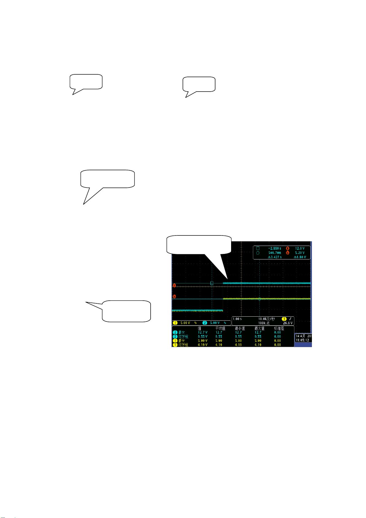
5.4 12V to +5V test points and its wave shape
U16(RT8110)
Pin# Name Voltage
1 BOOT 12.1V
2 DRIVE 6.09V
3 FB 0.78V
4 VCC 5.31V
5 LGATE 3.85V
6 GND /0
7 UGATE 11.4V
8 PHASE 8.08V
Page 13
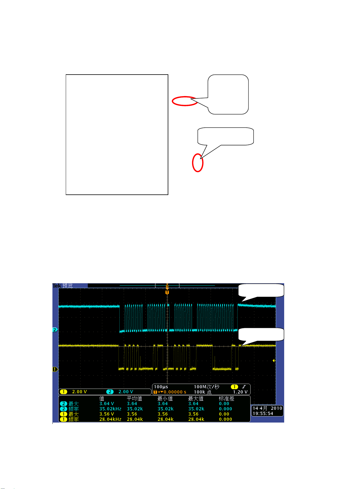
WAVE(L30)TO(L1)
13
UGATE
U33:(Pin3)5V
LGATE
12VTO5V
L1:OUTPUT
5V
Page 14
put
14
U9:5V TO
3.3V
L1: 5V
Out
U17:24VTO12V
5.5 12V to Tuner 5V test points and its wave shape
U1:12VTO
5V
Page 15
15
5.6 24V to 12V test points and its wave shape
U17(RT8110B)
Pin# Name Voltage
1 BOOT 5.07V
2 DRIVE 3.66V
3 FB 0
4 VCC 20.3V
5 LGATE 20.5V
6 GND 16.7V
7 UGATE 23.2V
8 PHASE 0.82V
UGATE LGATE
24VTO12V
WAVE(L113TOL109)
U17:24V
TO12V
Page 16
16
5.7 12V to 1V8 test points and its wave shape
U20(MP1484)
Pin# Name Voltage
1 BS 8.19V
2 IN 12.1V
3 SW 5.04V
4 GND 0
5 FB 0.93V
6 COMP 1.01V
7 EN 7.58V
8 SS 3.62V
U20 :12V
TO 1V8
12VTO1.8V
WAVE(L109TOC560)
+)
5.8 AV33/AV25/AV125/DV33/DV11 test points and its wave shape
Page 17

17
U21(MP1484)
Pin# Name Voltage
1 BS 6.69V
2 IN 12.1V
3 SW 4.06V
4 GND 0
5 FB 0.92V
6 COMP 1.06V
7 EN 7.58V
8 SS 3.64V
Page 18

18
U31 5VTOAV/3.3V
U9:5VTOD
V/3.3V
3V3VTO1.25V
WAVE( U7: 3TO 2)
12VTO1.8V
U21:12VT
ODV/1.1V
5VTODV3.3VWAV
E(U9:3TO2)+)
U7:3V3TO
1.25V
U6:5VTO2.5V
Page 19
5VTO2.5V
19
WAVE(U6 :3TO2 )
12VTO1.8V
5VTOAV3.3V
WAVE(U31:3TO
2)
12VTO1.8V
5.9 Main IC key test points and its wave shape
X27M2:crysta
l Oscillator
C503:
C524:
U14:
X27M1:crysta
l Oscillator
C167:
C168:
Q10:PanelDim
U14Main
Program
L85:DDRV1.8V
Q19:Reset
Transistor
U24
EEPROM
UpdateOnline:3.3v
R78,R80
Page 20
Q15:Pwr-Pr
20
otect
C:Pole 3.0V
MEMC:3.3V,SDA,SCL
U24: System EEPROM’s wave shape (Only while RCU or Key is pressing)
Pin_6:SCL
Pin_5:SDA
:
Page 21

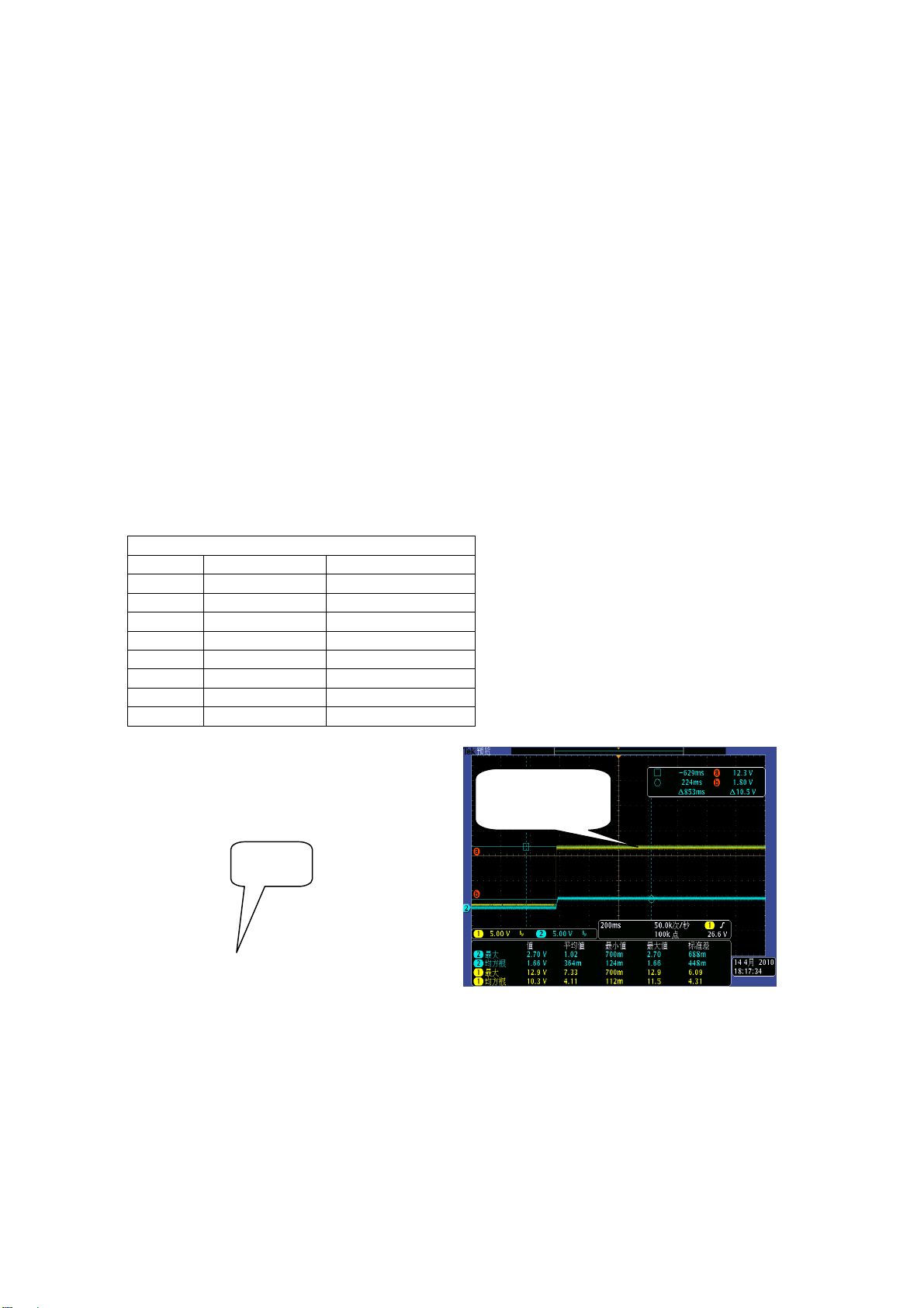
5.10 Start up test points while power on
21
Page 22

5.11 T-CON power supply test points
22
Q1:AO4459
Q14:BT390
L55/L56:12V
Page 23

Q14(B)toQ1(
23
5\6\7\8)
WAVE
5.12 DDR IC key test points
RM90\RM91 (MEMC DDR)
MVREFof UM21 Reference Voltage
0.92V
R292\R293
MVREFof U12\U13 Reference
Voltage 0.92V
Page 24
5.13 Tuner key test points
24
TU1
PIN# Name Function Voltage
1 ATN_PWR NC
2 B1 TUNER_5V 5.02V
3 RF-AGC RF Auto gain control
4 SCL BUS CLK 3.31V
5 SDA BUS DATA 3.31V
6 B2 TUNER_5V 5.02V
7 VTU-TP NC
8 AS GND 0
9 IF-AGC IF- Auto gain control 3.27V
10 DIF2 DIF Out Put 0.46
11 DIF1 DIF Out Put 0.46
12 AIF
5.14 HDMI input interface
Page 25

Q
12:HDMI5 Enable
(
25
HDMI 1-4:U23
Channel Switch from
Main IC
5.15 Power amplifier test points
U201)
Page 26

U700 sta3358w
26
Pin# Name Function Voltage
1 GND_SUB Substrate ground 0
2 SA I2C select address 0
3 TESTMODE This pin must be connected to ground 0
4 VSS Internal reference at Vcc-3.3 V 20.54V
5 VCC_REG Internal Vcc reference 23.82V
6 OUT2B Output half bridge 2B 0
7 GND2 Power negative supply 0
8 VCC2 Power positive supply 23.83V
9 OUT2A Output half bridge 2A 0
10 OUT1B Output half bridge 1B 0
11 VCC1 Power positive supply 23.83V
12 GND1 Power negative supply 0
13 OUT1A Output half bridge 1A 0
14 GND_REG Internal ground reference 0
15 VDD Internal 3.3 V reference voltage 3.27V
16 CONFIG Paralleled mode command 0
17 OUT3B PWM out CH3B – external bridge 0
18 OUT3A PWM out CH3A – external bridge 0
19 OUT4A Power down for external bridge 0
20 OUT4B Thermal warning from external bridge 0
21 VDD_DIG Digital supply voltage 3.20V
22 VSS_DIG Digital ground 0
23 POWERDN Power down
24 PLL_VDD Positive supply for PLL
25 PLL_FILTER Connection to PLL filter 0.3V
26 PLLGND Negative supply for PLL 0
27 XT1 PLL input clock
28 BICKL I2S serial clock 1.64V
29 LRCKL I2S left/right clock 1.63V
30 SDI I2S serial data channels 1 and 2 1.67V
31 RESET reset
32 INT_LINE Fault interrupt (0 = fault detected in the power
bridge, 1 = normal operation)
33 SDA I2C serial data 3.20V
34 SCL I2C serial clock 3.20V
35 GND_DIG Digital ground 0
36 VDD_DIG2 Digital supply voltage 3.2V
Page 27

5.16 AV out amplifier test points
27
If the AV audio no
output, please check
U25
L23: CVBS
U25(RC4558)
Pin# Name Voltage
1 1OUT 4.77V
2 1IN- 4.72V
3 1N+ 4.72V
4 VCC 0
5 VCC+ 4.72V
Page 28

6 2OUT 4.72V
28
7 2N- 4.77V
8 2N+ 9.50V
L165 or
L167 Point
Wave
AVOUT:
Wave of CVBS
At L23 Point
Page 29

6. Alignment Procedure
29
INFO:
All tests and measurements mentioned hereafter have to be carried out at a normal mains
voltage (220 ~ 240 VAC),
All voltages have to be measured with respect to ground, unless otherwise stated,
All final tests have to be done on a complete set including LCD panel in a room with
temperature of 25+/-7°C,
The White Balance (color temperature) has to be performed into subdued lighted room after
at least 1 hour of warm-up/burn-in. This is applicable for both Alignment and Picture
Performance evaluation at OQA in order to be set fr ee of any t emperature dr ift (colorimetr y vs
time).
1. Electrical Assembly Alignment
1.1. Preconditions – DC/DC Check
Before power on, please check the board according to the relevant block diagram and
circuit diagram, and make sure that no serious error should destroy the board. For
example, the output of DC/DC and LDO should not be shorted to ground. Supply a suited
voltage and power on, then check the voltage according to the relevant block diagram ,
circuit diagram and voltage spec. the error should less than 5% .For example, the voltage
for main chip(DV33, AV33,DV18,DV11,etc.), the voltage for DDR (DDRV) , the voltage
for amplifier(AUDIO_PWR),etc. Only the standby voltage is necessary if there is no
software in the flash.
1.2. Panel ID check and modify
There is different ID stored in the NVM depended on different Panels. Modify it with Hyper
terminal if the initial ID or a wrong ID make the set can not display clearly. It can be
checked and modified in Factory menu->Feature->Panel ID if the set can display clearly.
The set should be restart if the panel ID is changed.
1.3. Functional Test
Once the boards (chassis, KB, IR, PSU…) and the panel are well interconnected,
connect all external generator devices to relevant inputs/outputs below acc ording to their
respective test patterns format and check picture content and sound quality accordingly
Source
Analog /Digital Tuner RF cable Full Band (VHF/UHF) + CATV DVB-T
Test signal (generator) Test pattern (format/image)
:
Composite(CVBS) Chroma/Fluke PAL Half Color & Gray bars
SCART1 (CVBS)
SCART1 (RGB)
SCART2 (CVBS)
SCART2 (Y/C)
VGA Chroma/QuantumData 1024x768@60Hz Half Color & Gray bars
Chroma/Fluke PAL Half Color & Gray bars
Half Color & Gray bars
Chroma/Fluke PAL Half Color & Gray bars
Page 30

CMP (YPrPb) Chroma/QuantumData 1080i@60Hz Half Color & Gray bars
30
HDMI DVD with HDMI
compliancy
Headphone RF cable First channel
Loud Speake r s RF cable First chann e l
SCART1 (CVBS out) RF cable First channel
SCART2 (CVBS out) Chroma/Fluke PAL Half Color & Gray bars
Movie 720p@60Hz
Audio tones can be defined by the factory (ie: 1KHz & 3KHz, sweep, …).
Picture video formats can be changed by the factory according to their own standard.
1.4. ADC Calibration
To ensure the ADC performance, the error of “generator + cable” must be less than 2%. The
following inputs require an ADC calibration for the time being.
VGA (skip this step if no VGA input on the chassis)
Provide a test signal 1024×768@60Hz with White Black squares.
Select the corresponding Factory Menu->
press ”OK” key on
Remote Control to start. Value of status will change to “OK” if succeed.
ADC Calibration-> Auto Color , then
CMP
Provide a test signal 720p@60Hz with 100% 8 steps Color Bar.
Select the corresponding Factory Menu->
press ”OK” key on
Remote Control to start. Value of status will change to “OK” if succeed.
ADC Calibration-> Auto Color , then
Scart RGB
Provide a test signal PAL 576i with 100% 8 steps Color Bar.
Select the corresponding Factory Menu->
press ”OK” key on
The mean of status value:
“NONE”= no input is successful in ADC calibration.
“OK”= current input is successful in ADC calibration.
“NOK”= current input is fail in ADC calibration.
“ALL”= all inputs required are successful in ADC calibration.
Remote Control to start. Value of status will change to “OK” if succeed.
ADC Calibration-> Auto Color , then
R Gain, G Gain, B Gain, R Offset, G Offset, B Offset in Factory Menu-> ADC
Calibration page
can be fine-tuned if necessary but not required.
1.5. DDC & EDID Test
The E-EDID data structure are according to VESA Enhanced EDID 1.3 (and EIA/CEA-861B
for HDMI).
Both VGA and HDMI have their own separate bin files:
For EDID check, it’s needed to check whether the correct EDID is downloaded by checking
corresponding EDID NVM Checksum or read them out to check bit by bit if it is in line with the
released EDID bin file.
Page 31

1.6. HDCP Test
31
For HDCP compliancy, it’s needed to check whether the HDCP key has been well set.
1.7. CI+ Key activation and test (This step is only for the models with CI+
function )
Select factory men u-> Update CI+ Credential-> Update CI+ Crede ntial , then press ”OK”
key on
Cus Code(Custom Code), Serial Num display if succeed. Download the CI+ Key and try to
active it again if fail.
Remote Control to active the CI+ KEY. The Valid(CI+ state) state turn to “Yes” and
2. Final Assembly Alignment
2.1. Factory Menu
Follow the below steps to pop-up the Factory Menu in case of “Factory Key” is disabled:
press Remote Control key “MENU” to display main menu
-
- Select “Picture” and press “OK” key to enter the picture submenu
- Select “Contrast” item
- press the subsequence Remote Control keys “9”, “7”, “3” and “5”
Press Remote Control key “Blue” To pop-up the Factory Menu in case of “Factory
Key” is enabled.
The status of “Factory Key” can be changed in
Key
Press Remote Control “OK” key or “RIGHT” key to enter the submenu.
Press Remote Control “Menu” key to go back to the root menu.
Press Remote Control “RIGHT” or “LEFT” key to change the values.
Press Remote Control “OK” key run the function.
Press Remote Control “Exit” key exit the factory menu.
Factory Menu->System-> Factory
2.2. Entering to “P” Mode
Turned on the factory key to enter into “P” mode, The TV will display “P” in bottom left
corner in “P” mode.
2.3. White Balance Alignment
Make sure that the picture mode is “vivid”, enter to “P” mode (turned on the factory key) and
switch off “Pic. Enhance” in Factory Menu-> WD Alignment before white balance
alignment.
VGA,CMP,SCART RGB,DTV,CVBS_PAL Color Coordinates are relative to HDMI.
CVBS_SECAM and CVBS_NTSC Color Coordinates are relative to CVBS_PAL.
Warm and Cool Color Coordinates are relatives to Normal mode.
Only HDMI(YUV 720p@60Hz) input requires color temperature adjustment.
Matrix Offsets should be set while doing alignment.
All the Relative
“Factory Menu” Definition
1). System
Page 32

Item Sub-item Value Note
32
Factory Key Off/On
Power Mode Boot/
Standby/
Last Status
Burning Mode Off/On
Pre-Frequency
Run
OFF:hotkey is invalid
ON :hotkey(blue key) is availability
Boot: Enter power on mode
Standby: Enter standby mode
Last Status: power on acco rding to last status
Select panel On with left/right key, Press “EXIT”
key to enter the burning mode; Press “Menu” key
on keyboard to exit the burning mode
Press “OK” key to run
Poland
System
Pre-Frequency
Run
Press “OK” key to run
Huizhou
Pre-Frequency
Run
Press “OK” key to run
Thailand
Reset User
Reset All
Reset Shop
Clear date of NVM in user menu, except the value
of language / related installation/Factory setting,
then set to the default value.
clear NVM values,and set to default value。
Clear date of NVM in user menu, include the value
related installation, and Clear date of factory menu
except the item of Balance and sound ,set to
default value
2).Feature
Item Sub-item Value/Sub-item Note
Flesh Tone Off/On
Feature
Adaptive Luma
Control
Light sensor Off/On
Adaptive
Backlight
White Peak
Limitator
TunerAGC
Project ID ID
Off/On
Some models have no this feature.
Auto/Low/Mid/High (it
Set the backlight mode
should be “On/Off “ in 26
inch and smaller ones)
Backlight Low
Backlight Mid
Backlight High
ADP low control point
ADP mid control point
ADP high control point
Off/On
-44~127
Set the backlight value of Low mode
Set the backlight value of Mid mode
Set the backlight value of High (or Off)
mode
Set the low point in dynamic backlight
control curve
Set the mid point in dynamic backlight
control curve
Set the high point in dynamic backlight
control curve
Select panel ID with left/right key, restart
the set to take effect.
Page 33

/
33
There is no “Adaptive Backlight” item, “Auto/Low/Mid/High” “Backlight” “ADP low
control point” “ADP mid control point” “ADP high control point” are in the “feature”
page. There is only “Backlight” item instead of “Backlight Low” “Backlight Mid”
“Backlight High”. It set the backlight value of current backlight mode.
3). ADC Calibration
Item Sub-item Value Note
ADC Calibration
Source HDMI,etc
Auto color Run
Status NONE
/ NOK
/ OK
/ ALL
VGA\CMP\scart RGB require Calibration
Press “OK” key to run
NONE:No source has been calibrated
NOK:Current source hasn’t been calibrated
OK: Current source has been calibrated
ALL:All sources have been calibrated
R Gain
G Gain
B Gain
R Offset
For fine tune ADC manually.
G Offset
B Offset
4). WD Alignment
Item Sub-item Value Note
WD Alignment
Pic. Enhance ON/OFF
Source HDMI,etc
Press “Right” key to switch off all of the
items in the feature submenu. This should
be done before white balance alignment. If
it’s off, the way to switch it on is to reset
user/shop or set on the features in Feature
sub-item manually.
For balance source:
HDMI,VGA,DTV,PAL,SECAM,NTSC,Scart
RGB,CPM, HDMI
Color
Temperature
Normal
Warm/Cool
R Gain
G Gain
B Gain
R Offset
G Offset
B Offset
Scaling
Brightness
Scaling Contrast
Scaling Saturation
Auto phase Run
The value of Warm and cool is the offset of
Normal mode.
R White balance
G White balance
B White balance
R Gray balance
G Gray balance
B Gray balance
Press “OK” key to adjust the signal to
avoid the ripple in CMP source, it is not
necessary.
Page 34

34
5).Sound
Item Sub-item Value Note
Sound
VOL_0 0
VOL_10 5
VOL_50 20
VOL_90 145
VOL_100 255
6). Version info
Item Sub-item Value Note
Version info
Project: ***
Panel: ***
MT62 Ver: ***
Date: ***
MCU Ver: ***
7) . Update CI+ Creden t i a l (o n l y for the chassises wit h C I + function)
Item Sub-item Value Note
Update CI+
Credential
Update CI+ Credential DO
Update from USB DO
Erase CI+ Credential DO
Valid
Cus Code
Serial Num
Press “OK” key to active the CI+ KEY
Press “OK” key to download the CI+ KEY
from USB
Press “OK” key to erase the CI+ KEY
Show the CI+ state
Show the CI+ custom code
Show the CI+ serial number
Appendix “How to download MCU SW”
Prepare WT_MCU_ISP SW tool for update.
1. Connect the PC to the serial connector on board using a special serial device(USB
or COMx).
2. Provide the a correct voltage to the board.
3. Start “Weltrend MCU ISP.exe” and download the MCU SW.
Appendix “How to download FLASH SW”
Prepare MTK SW tool for update.
1. Connect the PC to the serial connector on board using a special serial device (USB or
COMx).
2. Provide the a correct voltage to the board
3. Start “MTKTOOL.exe” application under MTKxx folder, and set the parameters as
below picture(notice:select MT836X chassiss):
Page 35

35
4. Press “Browse” button to select the corresponding SW bin file to upload
5. Press “Upgrade” button to start downloading the SW and wait the gauge displayed
“100%” that means the SW has been successfully downloaded.
In the meanwhile, all operations such erasing flash and so… are parsed into the
debug window script.
6. Once the SW is downloaded, switch-off/on the chassis board and wait few seconds for
eeprom update.
Appendix” How to upgrade FLASH SW from USB”
1. Save the new software file(*.pkg) in the root directory of USB, and modify it’s name as
upgrade.pkg.
2. Plug in the USB.
3. Power on the set.
4. Press any key on keyboard and keep more than 2 second, about 5 second later , the
LED on IR board will flash after upgrade begin. The LED off if upgrade succeed. The LED
stop flashing and keep on if upgrade fail, check the set and try again.
If the set display normally, follow the indication instead of Step4.
Appendix “Modify panel ID with Hyper terminal”
①. Connect the PC to the board using a special serial device (USB or COMx).
②. Provide a correct voltage to the board
③. Save the password file “password for hyperTerminal.txt” to your computer.
④. Start HyperTerminal “HyperTrm.exe” in your computer.
⑤. Fill the name.
Page 36

36
⑥. Select the Com Port you are using.
⑦. Set the items as below picture
Page 37

Select “File->Save->” to Save the setting. Then start HyperTerminal “atsc.ht” in
37
your computer instead of step ③ to ⑦ later
⑧. Send the password.
⑨. Select the password file saved in your computer.
Page 38

⑩. Under the folder “DTV>” enter “pmx.s.p +ID”,e.g.: pmx.s.p 102
38
See the panel ID in another document <Panel list for MT62>.
⑪. Press “Enter”, the panel signal will be printed in the window
Page 39

Appendix “How to download FLASH SW for MEMC module”
39
Prepare MSTAR SW tool for update:
Install the driver:CDM_Setup.exe
Save the MS_TV folder to your PC,
1. Connect the PC to the I2C connector on board using a special I2C device (USB or
COMx).
2. Provide a correct voltage to the board.
3. Start “ISP_Tool.exe” application under MS_TV folder:
Page 40

4. Press “config” button On the Menu to enter the corresponding page, change the ISP
40
slave address to “0x94” and confirm that if the Port Type is correct, correct it if not.
5. Press “Read” button on the Menu to enter the corresponding page and Press “Read”
button on this page to load the software(*.bin) on your PC
6. Press “Auto” button on the Menu to enter the corresponding page
Page 41

7. Press “Conect” button on the Menu. A message will popup to tell you the result. Press
41
“OK” button to close the message. If fail to connect with “Can’t find the Device Ty pe!! ”
Message ,Check the hardware and parameters setting of the ISP_Tool , Press “Dis
Con” button , then “Conect” button again, until it identify the flash memory IC.
8. Press “Run” button in the current page to download the software.”Pass” will display on
the right bottom corner if succeed.
Page 42

42
Page 43

7. Project ID List
43
Panel ID Model
141 32Fs6646 32S6AUC T315HW05_V0 PANEL_AUO_32_T315HW05_V0 1920*1080
142 46Fs6646 46S6SSF LTA460HJ09 PANEL_SS_46_LTA_460_HJ09 1920*1080
143 40Fs6646 40S6SSM LTA400HF16 PANEL_SS_40_LTA_400_HF16 1920*1080
146 55FS6646 55S6SS4 LTA550HJ05 PANEL_SS_55_LTA_550_HJ05 1920*1080
148 37FS6646 37S6AUB T370HW04_V0 PANEL_AUO_37_T370HW04_V0 1920*1080
Project ID
factory menu
Panel name
factory menu
Panel Model Resolution
Notice:
There are two ways to change the panel ID.
1. Use line command in HyperTerminal as "pmx.s.p Panel ID";
2. Use factory menu. "Factory menu -> Feature -> Project ID", Please AC reset after change Project ID.
Page 44

8. Trouble Shooting
44
1.
Standby power OK, no
Power ON signal
Replace L44
Replace U201 or
X54M
Replace Q100
NO
Check L44
3.3V OK?
NO
NO
Check U201
and X54M
Check Q100 C
3.3V OK?
Check and repair the
Peripheral components
Page 45

2.
45
Replace Q9
Replace Q10
Replace Q14
Replace Q1
Power OK,no backlight,no raster
NO
Check Q9 C
high voltage ?
NO
NO
NO
Check and repair the PM2
PM4
Check Q10 C high
voltage ?
Check Q14
Pole C 0V
Check Q1
Pin8 12V
Page 46

3.
T
46
Replace Q14
R18
ReplaceL140
/L139
Replace Q1
NO
NO
NO
Power OK,backlight OK,no raster
Check Q14
Pole C 0V
Check Q1
Pin 1 12V
CheckQ1
Pin 8 12V
Check the
voltage of
LVDS signal
Replace LVDS cable
-CON board
or
Page 47

4.
b
47
Update the
software of U14
Replace Q1
Replace T-CON
board cable
NO
All source no picture
Software of U14
OK?
NO
NO
Replace U12/U13 or main
oard
USB no picture
Check L108
OK?
Check
U201 OK?
Check the
T-CON board
OK?
NO
AV no picture
Check circuit
from scart to
U201
replace
VGA no picture
VGA no picture
Check Q37 and
U29’VCC
NO
replace
HDMI5 no picture
Check Q16 and
U26 OK?
NO
replace
HDMI1-4 no picture
Check U23
OK?
NO
NO
replace
replace
Page 48

5.
48
Replace
L119,L135
Check the components from
FAT- to FAT_INPUTCheck the components from
FAT+ to FAT_INPUT+
Replace X54M
and U201
NO
TV no picture
Check TU1
pin_6 is 5V
NO
NO
Check TU1 pin_10
pin_11
Replace TU1
Page 49

6.
49
Replace U201
Replace U25
Replace L6
Replace L7 or
L5
Check speaker
cables or speaker
Picture ok, all source no sound
NO
Check R190 and
R191 ok?
NO
NO
NO
NO
Check L165
and L167 ok?
Check L6 3.3v
OK?
Check L5 and
L7
Check Q700
Pole C is low
Check Q700, Q701,Q915
Page 50

9. Key Spare Parts List
50
PART NUMBER DESCRIPTION NOTE
S8-32P116V-FC1 ASS'Y - FRONT CABINETASY 32W
S8-40P116V-FC1 ASS'Y - FRONT CABINETASY 40W
S8-46P116V-FC1 ASS'Y - FRONT CABINETASY 46W
S8-32P116V-RC1 ASS'Y - REAR CABINETASY 32W
S8-40P116V-RC1 ASS'Y - REAR CABINETASY 40W
S8-46P116V-RC1 ASS'Y - REAR CABINETASY 46W
02-891320-0001ACK PAI STAND 32P11 BASE CK -- 00 00 00 R=Y 32W
02-891330-0001ACK EQU STAND -- R=Y 40W
02-891340-0001ACK PAI STAND 46P11 -- CK 00 00 R=Y 46W
08-46P116V-IR100AA ASS'Y - INFRARED RECEIVE BDEQU
08-46P116V-KE200AA ASS'Y - KEY BDEQU
08-MT62S02-MA200AA ASS'Y - MAIN BDEQU 32/46W
08-MT62S06-MA200AA ASS'Y - MAIN BDEQU 40W
08-PE421C0-PW200AA ASS'Y - POWER BD(PWE4210)EQU 40/46W
08-PE321C0-PW200AA ASS'Y - POWER BD(PWE3210)EQU 32W
4A-LCD32T-AUC DISPLAY LCD PANEL 32INCH T315HW05 V0 R=Y 32W
4A-LCD40T-SSM DISPLAY LCD PANEL 40INCH LTA400HF16 R=Y 40W
4A-LCD46T-SSF DISPLAY LCD PANEL 46INCH LTA460HJ09 R=Y 46W
46-FB50DL-AU7L1G WIRE CONNECT PANEL TO MB 500MM 40 SR SR 32W
46-HB50DL-AU7L1G WIRE CONNET PANEL TO MB 500MM 34 SR SR 2 32W
46-FB065D-SSXM1G WIRE LVDS CABLE 650MM 51 PHD FI-RE51HL 2.0MM 40W
46-FB065D-SSXM1G WIRE LVDS CABLE 650MM 51 PHD FI-RE51HL 2.0MM 46W
46-LL050L-16X02G WIRE FROM PSU TO MB 500MM 12 PHD PHD 2.0
46-FL025L-28X02G WIRE INVERTER 250MM 28 PH PH 2.0MM UL265 32W
46-LF022T-28Q01G WIRE INVERTER WIRE 220MM 14 PH PHD 2MM U 46W
51-DC0180-0CR0FG POWER CORD 1800MM LP-21&H03VVH2-F 2C 6
42-WDF310-BOXG SPEAKER 16OHM 10W 150HZ RECTANGLE FBN003 32W
42-WDF313-BOXG SPEAKER 16OHM 10W 215HZ RECTANGLE FBN004 40/46W
72-MT62FS-EUM1A IB INSTRUCTION BOOK THOMSON R=Y
06-519W49-A040X RCT MT62S PHILIPS
07-361AI5-TA3G TUNER D% DIGIT 36.13HZ IEC DT70WI-3
13-MT5362-ANB IC-CHIPSET MT5362 R=Y
13-MT8295-BNB IC MT62 SERIES DVB-C CI INTERFACE
13-MX25L1-0GB IC MT62 FLASH BULK BGA:CSP 24BALL MX25L1
13-RT8110-00B IC 12V TO 5V CONVERTER RT8110
13-SII918-7AB IC MT5305A ATSC HDMI SWITCH 4 TO 1
13-STA335-BWB IC-AUDIO AUDIO IC
13-STV029-7EB IC MT62 DVB-C CHANNEL DECODER T
13-W25X40-AVB IC STORE SOFTWARE CODE W25X40AVSNIG
Page 51

13-TPS255-0DB IC OVERCURRENT PROTECT
51
13-M24C16-MNB IC 16K EEPROM M24C16-MN6
13-MP1482-DSB IC DC RECTIFIED STEP-DOWN CONVERTER
13-MST6M2-0SB OPTICOUP MS58 MEMC 216-PIN LQFP MST
13-AT24C0-2BB ATMEL 2K EERROM AT24C02BN-10SU-1.8 WRITE
13-AZ1084-33B IC AZ1084S2-3.3E1
13-EF4052-BTB TCL13-EF4052-BTB= IC HEF4052BT(D) R=N
13-H5PS51-62B IC MT62 MT8215 DDR FBGA FBGA H5PS5162F(L
12-13N03L-0BX MOSFET-SMD N 30V 10.4AA 3.57W SO8 PHKD13
12-81725W-0BX NPN TRANSISTOR BC817-25W
12-A04459-0BX MOSFET-SMD 30V 6.5A
12-BC857B-0BX PNP SMD. TRANSISTOR BC857B 215
12-BT3904-0BX TR-SMD NPN 40VV 200MA_A 300HZ 0.25W SOT2
12-BT3906-0BX TR-SMD PNP 40V 200MI0_A 250MHZ 225MI0W S
09-0BAV70-ATX D,SMD 75VV 125MA_A 715MVV 4N 0.25W SOT23
09-0BAV99-ATX D,SMD 70.0V 200MI0_A 855MI0V 4N 0.25W SO
09-55C5V1-DTX SMD.DIODE BZV55-C5V1
09-55C6V8-DTX SMD.DIODE 6.8V BZV55-C6V8
09-LL4148-ATX SMD. SWITCHING DIODE LL4148
45-OSC12M-0Y9C CRYSTAL HC-49/SMD12M
45-OSC27M-0Y7BB CRYSTAL 7C27000143BHAF25Q5
45-OSC54M-0Y1CR CRYSTAL 54MHZ 30PPM FUND 16P_F MST BREDE
10. Schematic Diagram
10.1 MT5362 GPIO Definition:
Pin Name Net Name Function Definition
GPIO0 GPIO_0 FOR MT8295 CHIP SELECT
GPIO1 strap(3) GPIO_1 FOR LV DS POWER CONTRAL
GP106 GPIO_6 USB_POWER ENABLE
GP107 GPIO_7 Inverter Dimming
GP108 GPIO_8 Reset STV0297E
GP109 GPIO_9 PANEL Backlight Power On/Off
GP110 GPIO_10 MT8295_RESE
GP112 GPIO_12 Reset DVBS Tuner
GP113 GPIO_13 For MT8295, CI_INT
GP114 GPIO_14 IPTV HDMI HPD
ADIN1 KEY KEY IN
ADIN2 ADIN2 LIGHT SENSOR
ADIN3 ADIN3 SCART FS
ADIN4 PWR_PROTECT POWER PROTECT
ADIN5 ADIN5 MUTE AMP
OPCTRL1 OPCTRL1 MT62 RESE T CONTRAL
Page 52

OPCTRL2 OPCTRL2 SYSTEM EEPROM WP
52
OPCTRL3(strap4) OPCTRL3 STRAP
OPCTRL5 OPCTRL5 STANDBY LED
OPWM0 strap(1) OPWM0
OPWM1 strap(0) OPWM1
OPWM2 OPWM2 TCL LOGO Light
OSDA0 OSDA0 SYSTEM SDA
OSCL0 OSCL0 SYSTEM SCL
OSDA1 OSDA1
OSCL1 OSCL1
OPWRSB POWER_ON/OFF POWER ON/OFF
ASPDIF ASPDIF SPDIF OUT
10.2 Summary:
Part 1: POWER SUPPLY INTERFACE AND CIRCUIT
Part 2: CONNECTORS AND KEY&IR CIRCUIT
Part 3: FLASH
Part 4: DDR
Part 5: RESET/CRYS/JTAG AND USB
Part 6: LVDS OUTPUT
Part 7: VGA INPUT
Part 8: SCART INPUT
Part 9: CMP INPUT, S/PDIF, IPTV CONNECTOR
Part 10: AUDIO IN SWITCH AND SCART AUDIO OUTPUT
Part 11: AUDIO AMPLIFIER CIRCUIT
Part 12: HDMI SOCKET AND SI9187 SWITCH
Part 13: CI SOCKET AND MT8285
Part 14: DVB-C DEMO
Part 15: DVB-T/C TUNER
Part 16: DVB-S TUNER
Part 17: MST6M20S AND DDR
Part 18: LVDS OUTPUT FROM MST6M20S
Part 19: POWER FOR LVDS
10.3 Schematic Diagram
Page 53

8 7 6 5
53
12V
L29
200R
L30
4U7
C52
200R
L32
0.1U
200R
L33
200R
C244
+5V
T
6V3
LD1117S33
U9
Z50
100U
C70
VIN
3
0.1U
4
4
OUT
2
C236
GND/ADJ
1
U33
NC/AIC1084
VOUTVIN
ADJ/GND
1
DV33A
T
4
4
OUT
2
DV33
GND/ADJ
1
LD1117S
U7
L34
200R
VIN
3
100U
C72
DV33A
0.1U
Z22
T
C234
23
6V3
R6
330R
AV33A
T
F
10R
C230
L1
15UH
R456
C231
0.1U
R448
10K
D11
C
BT3904
Q47
B
E
C250
1U
E
LL4148
GND
U16
1
BOOT
2
3 6
4
PHASE
DRIVE
UGATE
FB GND
LGATE
VCC
RT8110
8
7
5
GND
4
S2
3
G1
S1
G2
2
1
about 1mm
D13N03LT
Q38
D2B
D2A
D1B
D1A
5
6
7
8
0.1U
C243
0.01U
4U7
C53
R445
220R
GND
1K2
R459
C123
470U
6V3
6V3
C563
470U
4 3 2 1
Z66
T
DV11
L130
10UH
C450
0.1U
L38
0R
R106
0R
AV125
T
AV125
12V
L150
30R
16V
C83
100U
C50
4U7
C451
0.1U
C251
0.01U
100K
U21
1
BS
2
IN
3
SW COMP
GND
MP1484
R557
SS
EN
FB
8
7
6
54
C175
NC/3300P
D24
NC/SK24
GND
C248
C252
3300P
2K2
R480
0.1U
L9
15UH
220P
C449
R485
2K
10K
R484
4U7
C61
6V3
C561
470U
F
E
100U
4
U6
0.1U
VIN
3
U31
ADJ/GND
VIN
3
4
GND/ADJ
OUT
2
AZ1084
1
4
4
OUT
2
1
VOUTVIN
GND/ADJ
1
23
100U
6V3
R5
2R7
C80
100U
6V3
AV25
T
C81
R1
2R7
AV33A
0.1U
AV25
0.1U
0.1U
C232
C239
L94
200R
C237
U8
1000P
C440
GND
L95
120R
+3V3SB
STB_PWR
D
12V
R52
10R
R3
10R
C19
100U
16V
C872
100U
6V3
10R
R51
0.1U
3
C826
U811
NC/RT9166-33
IN OUT
GND
1
Z23
T
U1
8V
C115
16V
47U
VIN
3
2
0.1U
4
4
OUT
2
C136
C809
NC/100U
GND/ADJ
1
T
6V3
LD1117S50
16V
NC/0.1U
C825
C18
100U
TUNER_5V
0.1U
C135
+3V3SB
C824
1U
TUNER_5V
T
GND
NC/LD1117S33
6V3
47U
C461
C235
0.1U
LD1117S25
C238
R2
C71
6V3
120R
AV33
24V_MAYBE
C
C245
0.1U
L113
200R
L114
200R
35V
C13
220U
35V
C14
220U
C608
1U
C62
1U
0.1U
C204
0.1U
C377
LL4148
U17 RT8110B
BOOTFBUGATE
5
6
VIN
7
8
D7
D13N03LT
G2
4
GNDPHASE
3
LGATE
2
VCC
1
C203
2U2
dlt I=0.8*(0.36+5.1)/0.36=12.13
4
S2
3
G1
S1
2
1
Q6
D2B
D2A
D1B
D1A
D
dlt I=0.3*4.5A
L=12*(1-12/24)/(0.4*1.35)=11UH
Max 5.4A 17mo
5
6
7
8
0.033U
C207
L3510UH
R140
2R2
C208
0.015U
R142
5K1
L84
C577
470U
R141
360R
+/-1%
10UH
Z25
T
6V3
Z146
T
MEMC_DDR2_1V8
L109
L112
C63
10U
200R
200R
C378
0.1U
12V
C
Z67
L14
NC/15UH
12V
Z24
T
DV11_B
12V
B
L141
30R
16V
100U
C128
C16
4U7
C376
0.1U
C196
0.01U
1
2
3
R133
100K
U2
BS
IN
SW COMP
GND
SS
EN
FB
MP1484
8
7
6
54
C202
NC/3300P
D22
3300P
2K2
NC/SK24
GND
0.22U
C11
C197
R134
L2
15UH
220P
C334
R139
2K10K
R135
4U7
C201
6V3
C12
470U
C341
0.1U
...
DD-MM
...
...
L118
30R
16V
100U
C82
...
0.1U
C172
C446
4U7
C219
0.01U
SBU :
1
2
3
R483
100K
U20
BS
IN
SW COMP
GND
MP1484
SS
EN
FB
8
7
6
54
C174
D23
NC/SK24
GND
NC/3300P
L8
15UH
C246
3300P
2K2
R482
0.1U
C241
R107
510K
R555
10K
R556
10K
4U7
C60
6V3
C560
470U
1V8
C448
0.1U
L85
10UH
T
DDRV
B
A
THIS DRAWING CANNOT BE COMMUNICATED TO UNAUTHORIZED PERSONS COPIED UNLES S PERMITTED IN WRITING
For DVBS, NC
...
...
...
Index-Lab
DD-MM
DD-MM
DD-MM
DATE
...
...
...
Last saved :
5
...
...
...
DESCRIPTION Last modifNAME
5-5-2008_15:52
4678
...
...
...
TCLNO:
.............
DESIGNATION
...........
ON:
BY:
DRAWN
TCL Thomson Electronics Ltd.
B Building, TCL Tower, Nanhai Road
Nanshan District, Shenzhen, Guangdong
Tel +86-755-3331xxxx Fax +86-755-3331xxxx
CHECKED
DD-MM-YY
ON:
BY:
......
PAGE:
OF :
A
3 2 1
FORMAT DIN A2
Page 54

8 7 6 5
54
4 3 2 1
F
STB_PWR
+3V3SB
10K
B
OPWM2
R326
0R
E
C
BC857B
Q21
0R
R474K7
R1003
B
C
BT3904
E
GND
R85
NC/3K3
Q23
IR
KEY
R325
R42
3K3
E
OPCTRL5
R84K7
C
Q18
B
BT3904
E
GND
R336
3K3
0R
C3
NC/10U
R338
L146
STB_PWR
600R
STB_PWR
NC/10K
R337
STB_PWR
R334
NC/10K
L137
10K
R332
L143
600R
L142
600R
STB_PWR
600R
R335
NC/100K
LIGHT_SENSER
L138
600R
C331
1000P
L136
L144
C209
1U
600R
600R
C326
1000P
C327
1000P
R700
10K
C308
470P
C328
1000P
C290
1000P
R55
V270RA
2 1
F38
L_SENSOR
STB_PWR_OUT
IR_IN
LED_KEY
LED_LOGO
KEY_IN
STB_PWR_OUT1
LIGHT_SENSER
T
STB_PWR
T
IR_IN
T
LED_RED
T
STB_PWR_OUT1
L_SENSOR
L_SENSOR
STB_PWR
IR_IN
IR_IN
GND
LED_LOGO
LED_LOGO
GND
1 2
3
5
7
9
P5
LED_KEY
LED_KEY
KEY_IN
KEY_IN
4
6
GND
STB_PWR_OUT
8
STB_PWR
10
LED_KEY
T
KEY_IN
T
GND
T
STB_PWR2
T
F
E
R584,C539 FOR PWM TOUCH KEY ONLY,R504 IS 0 OHM IN OTHER KEY MODE.
D
12V
Z36
Z27
T
DIM
Z26
T
24V_MAYBE
T
Z6
L115
200R
PANEL_DIM
AUDIO_PWR
R25
STB_PWR
T
24V_MAYBE
C383
0.1U
0R
Z32
C382
0.1U
AUDIO_PWR
12V
R9
NC/0R
R10
NC/0R
STB_PWR_IN
0.1U
C381
PANEL_DIM
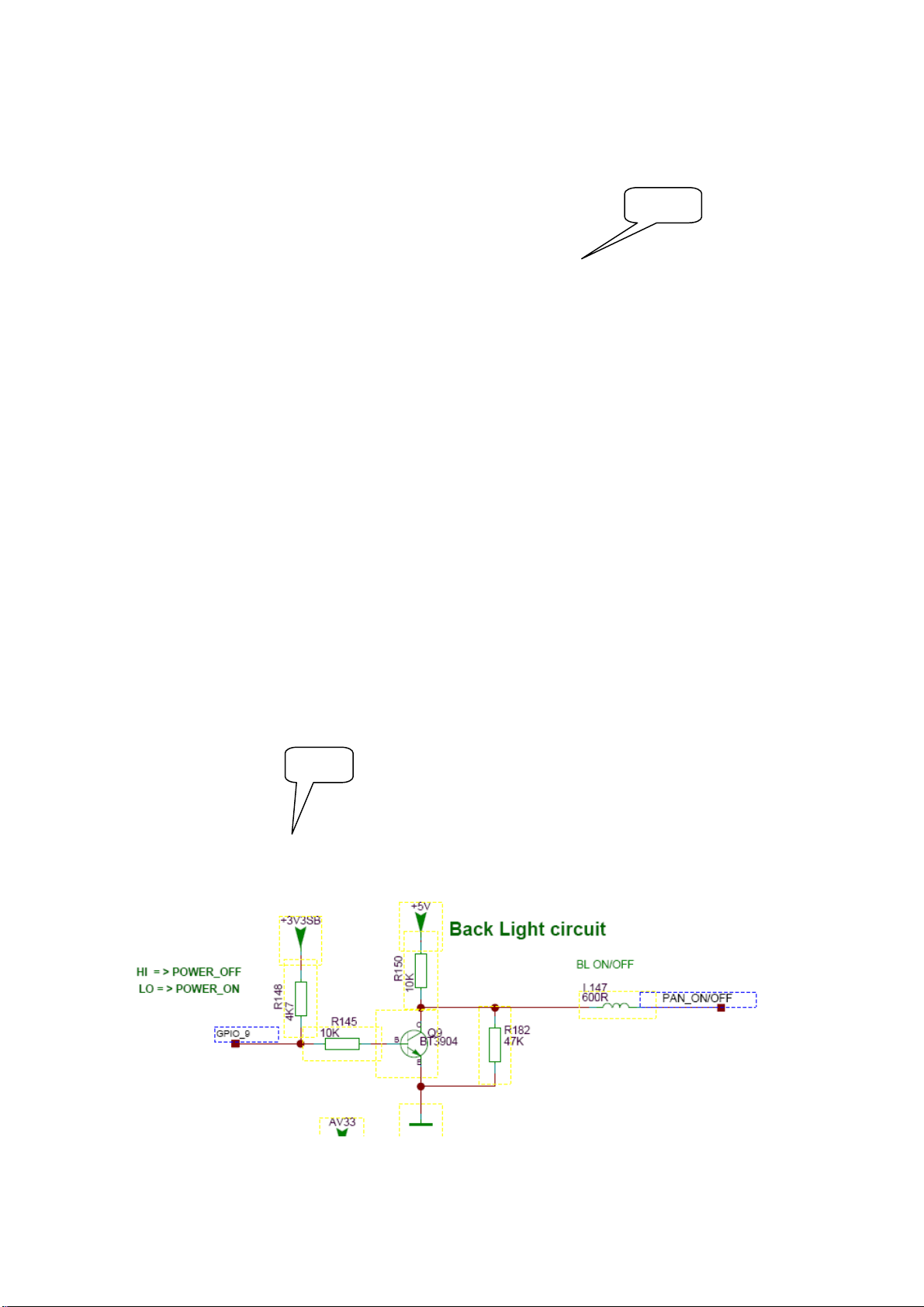
PAN_ON/OFF
0.1U
C380
0.1U
C379
ON/OFF_PWR
0.1U
C384
HI = > POWER_OFF
LO = > POWER_ON
GPIO_9
GPIO_7
10K
R170
+3V3SB
R148
4K7
R149
4K7
10K
+5V
R145
AV33
R156
NC/0R
3K9
R150
B
R181
R144
+5V
Back Light circuit
10K
C
BT3904
E
NC/1K
B
Q9
C
E
Q10
BT3904
D19
LL4148
6K8
R183
R182
47K
C210
1U
BL ON/OFF
L147
600R
DIMMING
600R
L148
PAN_ON/OFF
R1001
NC/0R
R1002
NC/0R
PANEL_DIM
PANEL_DIM2
VBR_EXT
+5V
CI_VCC
TUNER_5V
8V
DV33
AV33
AV25
D18
LL4148
D10
NC/LL4148
D13
LL4148
LL4148
D15
LL4148
D14
LL4148
D8
LL4148
D12
8K2
R236
R205
2K2
R204
1K8
R206
4K7
+3V3SB
B
R212
E
C
4K7
Q15
BT3906
R220
4K7
PWR_PROTECT
T
AUDIO_PWR
12
P19
GND
3
5
7
9
11
13
15
GND
24V_MAYBE
Z29
Z28
STB POWER
T
T
ON/OFF_PWR
PAN_ON/OFF
GND
4
6
8
10
12
14
16
STB_PWR_IN
C
ON/OFF_PWR
PAN_ON/OFF
B
D
C
B
A
THIS DRAWING CANNOT BE COMMUNICATED TO UNAUTHORIZED PERSONS COPIED UNLES S PERMITTED IN WRITING
R231
2K2
...
...
...
...
Index-Lab
Last saved :
5
DD-MM
DD-MM
DD-MM
DD-MM
DATE
...
...
...
...
...
...
...
...
DESCRIPTION Last modifNAME
5-5-2008_15:52
4678
...
...
...
...
SBU :
TCLNO:
.............
DESIGNATION
...........
ON:
BY:
DRAWN
TCL Thomson Electronics Ltd.
B Building, TCL Tower, Nanhai Road
Nanshan District, Shenzhen, Guangdong
Tel +86-755-3331xxxx Fax +86-755-3331xxxx
CHECKED
DD-MM-YY
ON:
BY:
......
PAGE:
OF :
A
3 2 1
FORMAT DIN A2
Page 55

8 7 6 5
55
4 3 2 1
U14
A1
NC1
F
DV11
DV33
C73
47U
6V3
C192
NC/4U7
DV33
1U
C90
C268
0.1U
C263
0.1U
C264
0.1U
C265
0.1U
C266
0.1U
C267
0.1U
C279
0.1U
C269
0.1U
C270
0.1U
C280
0.01U
Bottom SideCORE BYPASS
C271
0.1U
C272
0.1U
C281
3300P
C273
0.1U
C274
0.1U
C275
0.1U
DV33
L110
600R
Z199
T
C223
0.1U
4K7
R157
DV33S
T
POOE#
GND
POCE0#
Z197
FRESET#
A2
NC2
A3
NC3
A4
NC4
B1
NC5
B2
SCLK
B3
GND
B4 E1
VCC NC9
C1
NC6
C2
CS#
C3
NC7
C4
WP#SIO2
MX25L6455
NC16
NC15
NC14
NC13
NC12
NC11
NC10
NC/SIO3
SI/SIO0
SO/SIO1
NC8
F4
F3
F2
F1
E4
E3
E2
D4
D3
D2
D1
F
PDD1
PDD0
E
C91
1U
AOLRCKAOBCKOPWM2Strapping Mode
Normal mode 0
ICE mode
CPU model mode 0
0
0 1
Trap Mode
Core Reset 1us
Core Reset 3.3V
SCAN mode
Core Reset 0.9V
0
0 1
1
1 1
Strapping Mode
XTAL 54MHz
XTAL 27MHz
0 0
1
Strapping Mode
Nor Boot
NAND Boot
large NAND Boot
0 0
0 1
1
0 0
0 1
OPCTRL4OPCTRL5
0
0
OPCTRL2(O)OPCTRL3(O)
0
OPWM1(O)OPWM0(O)
0
DV33
DV11
Z65
DV33
POCE0#
PACLE
PAALE
POWE#
PDD6
PDD7
POOE#
PARB#
PDD2
PDD5
PDD4
PDD3
PDD1
POCE1#
T
PDD0
AC5
AB6
C6
C7
D7
E7
C8
D8
E8
K10
R10
U10
L11
P11
R11
U11
V12
U13
V14
L15
U15
K16
V16
L17
N17
R17
U17
V17
K18
M18
P18
T18
A16
B17
C17
D17
A18
B18
C18
D18
A19
B19
C19
D19
E19
C20
D20
F18
F19
F21
F22
U201
VCC3IO
VCC3IO1
VCCK
VCCK1
VCCK2
VCCK3
VCCK4
VCCK5
VCCK6
VCCK7
VCCK8
VCCK9
VCCK10
VCCK11
VCCK12
VCCK13
VCCK14
VCCK15
VCCK16
VCCK17
VCCK18
VCCK19
VCCK20
VCCK21
VCCK22
VCCK23
VCCK24
VCCK25
VCCK26
VCCK27
VCCK28
VCCK29
POCE0_
PACLE
PAALE
POWE_
PDD6
PDD7
POOE_
PARB_
PDD2
PDD5
PDD4
PDD3
PDD1
POCE1_
PDD0
VCC3IO_1
VCC3IO_1_1
VCC3IO_1_2
VCC3IO_1_3
DVSS
DVSS1
DVSS2
DVSS3
DVSS4
DVSS5
DVSS6
DVSS7
DVSS8
DVSS9
DVSS10
DVSS11
DVSS12
DVSS13
DVSS14
DVSS15
DVSS16
DVSS17
DVSS18
DVSS19
DVSS20
DVSS21
DVSS22
DVSS23
DVSS24
DVSS25
DVSS26
DVSS27
DVSS28
DVSS29
DVSS30
DVSS31
DVSS32
DVSS33
DVSS34
DVSS35
DVSS36
DVSS37
DVSS38
DVSS39
DVSS40
DVSS41
DVSS42
DVSS43
DVSS44
DVSS45
DVSS46
DVSS47
DVSS48
DVSS49
DVSS50
DVSS51
DVSS52
DVSS53
DVSS54
DVSS55
DVSS56
DVSS57
DVSS58
DVSS59
DVSS60
DVSS61
DVSS62
DVSS63
DVSS64
DVSS65
DVSS66
DVSS67
B1
C2
K2
U2
V2
D3
L3
V3
D4
L4
U4
E5
K5
T5
G6
T6
Y6
AA7
L10
P10
T10
M11
N11
T11
L12
M12
N12
P12
R12
T12
U12
L13
M13
N13
P13
R13
T13
L14
M14
N14
P14
R14
T14
U14
K15
M15
N15
P15
R15
T15
L16
M16
N16
P16
R16
T16
U16
F17
K17
M17
P17
T17
L18
N18
R18
U18
F20
E22
NC/4U7
C41
C276
0.1U
C282
3300P
I / O BYPASS
C277
0.1U
Bottom Side
D
C278
0.1U
MT5362 STRAPPING MODE
AOBCK
R1034K7
AOLRCK
4K7 R159
OPCTRL5
R1614K7
OPCTRL4
R1634K7
C
OPCTRL3
R1654K7
OPWM0
R1674K7
OPWM1
R1694K7
B
E
D
C
B
MT5362
A
THIS DRAWING CANNOT BE COMMUNICATED TO UNAUTHORIZED PERSONS COPIED UNLES S PERMITTED IN WRITING
...
...
...
...
Index-Lab
Last saved :
5
DD-MM
DD-MM
DD-MM
DD-MM
DATE
...
...
...
...
...
...
...
...
DESCRIPTION Last modifNAME
5-5-2008_15:52
4678
...
...
...
...
SBU :
TCLNO:
.............
DESIGNATION
...........
ON:
BY:
DRAWN
TCL Thomson Electronics Ltd.
B Building, TCL Tower, Nanhai Road
By Ada.Du
Nanshan District, Shenzhen, Guangdong
Tel +86-755-3331xxxx Fax +86-755-3331xxxx
CHECKED
DD-MM-YY
ON:
BY:
......
PAGE:
OF :
A
3 2 1
FORMAT DIN A2
Page 56

8 7 6 5
56
4 3 2 1
RDQS0
RDQS0#
RDQM0
RDQ0
RDQ1
RDQ2
F
E
RDQ3
RDQ4
RDQ5
RDQ6
RDQ7
RDQS1
RDQS1#
RDQM1
RDQ8
RDQ9
RDQ10
RDQ11
RDQ12
RDQ13
RDQ14
RDQ15
RDQS2
RDQS2#
RDQM2
RDQ16
RDQ17
RDQ18
RDQ19
RDQ20
RDQ21
RDQ22
RDQ23
RDQS3
RDQS3#
RDQM3
RDQ24
RDQ25
RDQ26
RDQ27
RDQ28
RDQ29
RDQ30
RDQ31
D
W1
W2
W4
W3
AA2
W5
D2
D1
E4
C4
B2
C3
A2
A4
D5
C1
B3
E1
E2
F5
G4
F3
F1
F2
E3
G3
F4
G5
U1
V1
V4
U3
T1
T4
T2
R3
R4
T3
R5
U5
Y2
Y3
V5
Y1
RDQS0
RDQS0_
RDQM0
RDQ0
RDQ1
RDQ2
RDQ3
RDQ4
RDQ5
RDQ6
RDQ7
RDQS1
RDQS1_
RDQM1
RDQ8
RDQ9
RDQ10
RDQ11
RDQ12
RDQ13
RDQ14
RDQ15
RDQS2
RDQS2_
RDQM2
RDQ16
RDQ17
RDQ18
RDQ19
RDQ20
RDQ21
RDQ22
RDQ23
RDQS3
RDQS3_
RDQM3
RDQ24
RDQ25
RDQ26
RDQ27
RDQ28
RDQ29
RDQ30
RDQ31
MT5362
REXTUP
REXTDN
AVSS12_MEMPLL
AVDD12_MEMPLL
VCC2IO22
VCC2IO21
VCC2IO20
VCC2IO19
VCC2IO18
VCC2IO17
VCC2IO16
VCC2IO15
VCC2IO14
VCC2IO13
VCC2IO12
VCC2IO11
VCC2IO10
VCC2IO9
VCC2IO8
VCC2IO7
VCC2IO6
VCC2IO5
VCC2IO4
VCC2IO3
VCC2IO2
VCC2IO1
RA12
RA11
RA10
RA9
RA8
RA7
RA6
RA5
RA4
RA3
RA2
RA1
RA0
RCS_
RRAS_
RCAS_
RWE_
RBA0
RBA1
RODT
RCLK1
RCLK1_
RCLK0
RCLK0_
RCKE
RVREF
VCC2IO
M1
K4
M5
M3
L5
M2
L2
M4
M6
N5
L1
N6
K3
J2
J4
J1
P1
N3
P2
J3
AB2
AB1
H2
H1
N4
P6
B5
A5
N10
M10
W6
V6
R6
J6
E6
D6
Y5
P5
J5
H5
C5
AA4
Y4
P4
H4
B4
AA3
P3
H3
A3
R2
N2
G2
RA12
RA11
RA10
RA9
RA8
RA7
RA6
RA5
RA4
RA3
RA2
RA1
RA0
RCS#
RRAS#
RCAS#
RWE#
RBA0
RBA1
RODT
RCLK1
RCLK1#
RCLK0
RCLK0#
RCKE
MEM_VREF
33R
AV12_MEMPLL
R172
DDRV
R171
33R
DDRV
MEM_VREF
RDQ15
RDQ14
RDQ13
RDQ12
RDQ11
RDQ10
RDQ9
RDQ8
RDQ7
RDQ6
RDQ5
RDQ4
RDQ3
RDQ2
RDQ1
RDQ0
C1
C3
C7
C9
G1
G3
G7
G9
M9
R1
A9
E9
A1
E1
D9
D1
D3
D7
C2
C8
H9
H1
H3
H7
G2
G8
J9
J1
J7
J2
B9
B1
F9
F1
VDDQ1
VDDQ2
VDDQ3
VDDQ4
VDDQ5
VDDQ6
VDDQ7
VDDQ8
VDDQ9
VDDQ10
VDD1
VDD2
VDD3
VDD4
VDD5
VDDL
VSSDL
VREF
DQ15
DQ14
DQ13
DQ12
DQ11
DQ10
DQ9
DQ8
DQ7
DQ6
DQ5
DQ4
DQ3
DQ2
DQ1
DQ0
HYB18TC512160BF
VSSQ10
VSSQ9
VSSQ8
VSSQ7
VSSQ5
VSSQ4
VSSQ3
VSSQ6
H8H2F8F2D8D2B8B2A7P9N1J3E3
E7
DDR#1
U12
VSSQ2
VSSQ1
VSS5
VSS4
VSS3
VSS2
ODT
BA1
BA0
NC/A13
A12
A11
A10
CS
RAS
CAS
UDM
LDM
WE
UDQS
UDQS
LDQS
LDQS
CKE
CK
VSS1
CK
A3
G1
G3
G7
G9
M9
A9
C1
C3
C7
C9
E9
A1
E1
R1
D9
D1
D3
D7
C2
C8
H9
H1
H3
H7
G2
G8
J9
J1
J7
J2
B9
B1
F9
F1
VDDQ1
VDDQ2
VDDQ3
VDDQ4
VDDQ5
VDDQ6
VDDQ7
VDDQ8
VDDQ9
VDDQ10
VDD1
VDD2
VDD3
VDD4
VDD5
VDDL
VSSDL
VREF
DQ15
DQ14
DQ13
DQ12
DQ11
DQ10
DQ9
DQ8
DQ7
DQ6
DQ5
DQ4
DQ3
DQ2
DQ1
DQ0
HYB18TC512160BF
VSSQ10
VSSQ9
VSSQ8
VSSQ7
VSSQ5
VSSQ4
VSSQ3
VSSQ6
H8H2F8F2D8D2B8B2A7P9N1J3E3
E7
U13
VSSQ2
VSSQ1
VSS5
VSS4
VSS3
VSS2
K9
MRODT
L3
MRBA1
L2
MRBA0
R8
R2
MRA12
P7
MRA11
M2
MRA10
P3
A9
A8
A7
A6
A5
A4
A3
A2
A1
A0
M7
M3
M8
L8
K7
L7
B3
F3
K3
B7
A8
F7
E8
K2
J8
K8
P8
P2
N7
N3
N8
N2
MRA9
MRA8
MRA7
MRA6
MRA5
MRA4
MRA3
MRA2
MRA1
MRA0
MRCS#
MRRAS#
MRCAS#
RDQM1
RDQM0
MRWE#
RDQS1
RDQS1#
RDQS0
RDQS0#
MRCKE
CLK0
DDRVDDRV
MEM_VREF
RDQ31
RDQ30
RDQ29
RDQ28
RDQ27
RDQ26
RDQ25
RDQ24
RDQ23
RDQ22
RDQ21
RDQ20
RDQ19
RDQ18
RDQ17
RDQ16
DDR#2
ODT
BA1
BA0
NC/A13
A12
A11
A10
CS
RAS
CAS
UDM
LDM
WE
UDQS
UDQS
LDQS
LDQS
CKE
CK
VSS1
CK
A3
K9
L3
L2
R8
R2
P7
M2
P3
A9
P8
A8
P2
A7
N7
A6
N3
A5
N8
A4
N2
A3
M7
A2
M3
A1
M8
A0
L8
K7
L7
B3
F3
K3
B7
A8
F7
E8
K2
J8
K8
MRODT
MRBA1
MRBA0
MRA12
MRA11
MRA10
MRA9
MRA8
MRA7
MRA6
MRA5
MRA4
MRA3
MRA2
MRA1
MRA0
MRCS#
MRRAS#
MRCAS#
RDQM3
RDQM2
MRWE#
RDQS3
RDQS3#
RDQS2
RDQS2#
MRCKE
CLK1
CLK1#CLK0#
NEAR IC
RCLK0
RCLK0#
RCLK1
RCLK1#
22R
22R
22R
22R
R538
R537
R535
R536
NEAR DRAM
CLK0
R486
100R
CLK0#
CLK1
R487
100R
CLK1#
NEAR IC
R173
MRODT
MRCAS#
MRCS#
MRA0
MRA6 RA6
MRA2
MRA7
MRBA0
MRCKE RCKE
MRWE#
22R
22R
1
3 6
R503 22R
1
3 6
22R
22R
MRRAS#
MRA8
MRA11
MRA4
R504
3 6
1
22R
MRA1
MRA9
MRA12
MRA5
R505
3 6
1
R502
R17822R
R177
R176
8
72
54
8
72
54
RODT
RWE#
RBA1MRBA1
54
72
8
54
72
8
RCAS#
RCS#
RA0
RBA0
RRAS#
RA2
RA7
RA8
RA11
RA4
RA1
RA9
RA12
RA5
F
E
22R
R174
22R
22R
R175
RA10MRA10
RA3MRA3
D
U201
DDRV
C77
100U
6V3
4U7
C96
C768
1U
C
AV125
B
C94
0.1U
L48
C228
NC/4U7
600R
C289
0.1U
C288
0.1U
AV12_MEMPLL
C229
NC/10U
C287
0.1U
C293
3300P
Bottom Side DDR#1
C93
0.1U
C286
0.1U
MEM_VREF
C319
0.1U
C285
0.1U
GND
C284
0.1U
C257
NC/4U7
C291
0.1U
C292
3300P
C95
1U
DDRV
DDRV
MEM_VREF
1K
R292
DDRV
C240
4U7
C78
100U
6V3
C767
NC/1U
4U7
C98
C312
0.1U
C765
NC/1U
C766
0.1U
C313
0.1U
C314
0.1U
C299
0.1U
0.1U
C315
3300P
DDR BYPASS BOTTOM SIDE
C300
C301
0.1U
3300P
Bottom Side DDR#2
C304
C309
0.1U
0.1U
C302
C303
0.1U
C296
0.1U
C295
0.1U
C310
0.1U
C294
0.1U
C311
3300P
0.1U
C316
0.1U
C297
C317
0.1U
C298
3300P
C318
0.1U
C99
1U
C361
3300P
C
C436
3300P
B
L49
600R
C321
0.1U
R293
1K
GND
GND
A
THIS DRAWING CANNOT BE COMMUNICATED TO UNAUTHORIZED PERSONS COPIED UNLES S PERMITTED IN WRITING
C320
0.1U
C101
0.1U
...
...
...
...
Index-Lab
Last saved :
5
DD-MM
DD-MM
DD-MM
DD-MM
DATE
...
...
...
...
...
...
...
...
DESCRIPTION Last modifNAME
5-5-2008_15:52
4678
...
...
...
...
SBU :
TCLNO:
.............
DESIGNATION
...........
ON:
BY:
DRAWN
TCL Thomson Electronics Ltd.
B Building, TCL Tower, Nanhai Road
By Rockie
Nanshan District, Shenzhen, Guangdong
Tel +86-755-3331xxxx Fax +86-755-3331xxxx
CHECKED
DD-MM-YY
ON:
BY:
......
PAGE:
OF :
A
3 2 1
FORMAT DIN A2
Page 57

57
8 7 6 5
54MHz CRYSTAL
R31
820K
SYSTEM EEPROM
F
X54M
OXTALI
54M
OXTALO
LO = > Wp
HI = > Write
L36
C385
10P
C399
10P
0.82UH
OPCTRL2
C532
1000P
+3V3SB
E
STB_PWR
12V
D
R430
NC/1K
R432
4K7
1K5
R429
2.9V(12V)
10U
C2
2.1V(9V)
33K
R425
R426
100K
B
R428
100R
E
C
R427
47K
Q19
2.7V
BT3906
C137
0.1U
10K
BT3906
Q17
R164
E
C
ORESET#
10P
C700
R160
R158
10K
100R/10K
B
MCU-RESET
T
System Reset#
+3V3SB
Z98
Z99
R78
R80
4K7
10P
4K7
C138
V270RA
R54
2 1
U0RX
C
U0TX
L82
L83
30R
30R
C139
10P
B
+5V
V270RA
R64
2 1
T
T
F10
USB PORT 0
R184
0R
DV33
U22
1
IN
2
GND
3
EN
NC/TPS2550
NC/24K
R147
HI = > NORMAL
LO=> OC
OSCL2
OUT
ILIM
FAULT
6
5
R179
NC/10K
4
C5
GPIO_6
HI = > POWER ON
LO = > POWER OFF
1U
R155
NC/0R
DV33
C191
R151
NC/0.1U
NC/10K
R180
NC/10K
A
THIS DRAWING CANNOT BE COMMUNICATED TO UNAUTHORIZED PERSONS COPIED UNLES S PERMITTED IN WRITING
C190 0.1U
L108
100K
R154
30R
6V3
C87
100U
R600
BT3904
Q11
+3V3SB
F15
0.1U
10K
C
E
3V3SB
RX
TX
GND
USB_DP0
USB_DM0
C156
NC/10P
BT3904
B
C452
B
1
2
3
4
R162
4K7
C
Q5
E
P16
USB_VCC
T T
OSCL0
OSDA0
V_TEST
USB_DP0
F1
R1194K7
T
OSDA0
USB_DM0
T
21
R12
R132
4K7
T
OSCL0
USB_GND
T
F2
DV33
R121
4K7
T
EWC
21
R13
33R
R104
C259
C153
NC/10P
47P
6
5
4
3
2
1
T
3V3
C140
C260
1000P
47P
JTAG Port
JTDO
MNT-HOLE2
MNT-HOLE1
GND-1
DPOS-1
DNEG-1
VCC-1
P7
Index-Lab
5
IIC ADDRESS "A0"
U24
8
7
6
5
VCC
WC
SCL
SDA
E0/NC
E1/NC
E2/NC
VSS
M24C16MN
STB
DV33
6
8
10K
R501
1
3
JTRST#
JTDI
JTMS
JTCK
R11733R
R122
10K
...
...
...
...
DD-MM
DD-MM
DD-MM
DD-MM
DATE
Last saved :
1
2
3
4
R1005
5472
...
...
...
...
1K
DV33
CB70
0.1U
R1006
NC/10K
ON/OFF
R1007
10K
C465
C454
10P
10P
...
...
...
...
DESCRIPTION Last modifNAME
5-5-2008_15:52
4 3 2 1
+3V3SB
AV125
GND
OPWM2
R109
4K7
PEND_MUTE
Z64
T
R116
4K7
LIGHT_SENSER
ADIN3
KEY
R146 180K
C536
1000P
R136
L45
C351
NC/4U7
100R
OPCTRL2
R143
STB
33R
PWR_PROTECT
R525
For 3.3V Tarp
5K1
0R
0R
USB_DM0
USB_DP0
REMARK=1%
ON:
BY:
L44
600R
4U7
Z55
Z20
Z56
Z58
Z59
Z142
Z141
Z60
R291
R222
R280
DRAWN
MUST NEAR IC
600R
AVDD33_XTAL
C27
1U
MUST NEAR IC
AVDD12_PLL
C31
JRTCK
T
JTDI
JTCK
OPWM1
OPWM0
JTMS
JTDO
JTRST#
VCXO
T
OSDA0
GPIO_6
PBS_TX
T
OSCL0
PBS_RX
T
GPIO_1
GPIO_19
GPIO_17
T
GPIO_18
GPIO_14
T
GPIO_15
GPIO_7
GPIO_16
GPIO_13
GPIO_12
GPIO_0
OSDA2
T
OSCL2
OIRO
T
GPIO_10
GPIO_9
GPIO_8
U0TX
U0RX
OPCTRL5
OPCTRL4
OPCTRL3
V_TEST
ORESET#
IR
C_XREG
AVDD12_PLL
AVDD12_PLL
AVDD12_PLL
AVDD12_PLL
AVDD12_PLL
AVDD12_PLL
ADIN5
180K
AVDD12_USB
AVDD33_USB
AVDD33_USB
Z53
T T
Z54
USB_VRT
OXTALI
AVDD33_XTAL
OXTALO
TCL Thomson Electronics Ltd.
B Building, TCL Tower, Nanhai Road
By Ada.Du
Nanshan District, Shenzhen, Guangdong
Tel +86-755-3331xxxx Fax +86-755-3331xxxx
C42
0.01U
AC1
AE1
AC2
AD2
AE2
AF2
AB3
AC3
AD3
AE3
AF3
AB4
AC4
AD4
AE4
AA5
AB5
AD5
AA6
A12
B14
A15
B15
B16
C16
D16
E16
E17
E18
E20
D21
E21
C22
D22
C23
D23
E23
AB8
AC8
AD8
AB9
AC9
AB10
AC10
AD10
AB11
AC11
AD11
V13
R23
N24
P24
R24
N25
N26
W23
W24
Y24
Y25
AA25
AA26
V10
AC6
AD6
AE5
AF5
AE6
AF6
AF4
V26
W25
V24
V25
AC7
AD7
V11
P22
N23
P23
CHECKED
DD-MM-YY
ON:
BY:
CB73
0.1U
CB78
0.1U
U201
JRTCK
OPWM2
JTDI
JTCK
OPWM1
OPWM0
JTMS
JTDO
JTRST_
VCXO
OSDA0
GPIO6
GPIO4
OSCL1
OSCL0
GPIO5
GPIO2
OSDA1
GPIO3
GPIO1
GPIO19
GPIO17
GPIO18
GPIO14
GPIO15
GPIO7
GPIO16
GPIO13
GPIO12
GPIO0
OSDA2
OSCL2
GPIO11
OIRO
GPIO10
GPIO9
GPIO8
U0TX
U0RX
OPCTRL5
OPCTRL4
OPCTRL3
OPCTRL2
OPCTRL1
OPCTRL0
ORESET_
OPWRSB
OIRI
AVDD12_LDO
AVDD12_DMPLL
AVDD12_ADCPLL
AVDD12_TVDPLL
AVDD12_DTDPLL
AVDD12_SYSPLL
AVDD12_APLL
ADIN5_SRV
ADIN4_SRV
ADIN2_SRV
ADIN3_SRV
ADIN1_SRV
ADIN0_SRV
AVDD12_USB
AVDD33_USB
AVDD33_USB1
USB_DM0
USB_DP0
USB_DM1
USB_DP1
USB_VRT
XTALI
AVSS33_XTAL
AVDD33_XTAL
XTALO
AVSS33_USB
AVSS33_USB1
AVSS12_USB
AVSS12_PLL
AVSS12_PLL1
AVSS12_PLL2
MT5362
......
C922
3300P
PAGE:
OF :
STB_PWR
B
C466
10P
4678
E
BT3906
Q100
C
ON/OFF_PWR
100K
R1008
GND
R123
10K
C464
10P
C467
10P
R111
1K
TVTREF#1
JTAG_DBGRQ
JTAG_DBGACK
R125
10K
...
...
...
...
AV33
AV125
ON/OFF
C360
R120
10K
L42
600R
600R
NC/0.1U
Z70
T TT
Z5
Z8
Z21
Z34
Z35
Z51
Z57
Z68
TTTTTTT
Z69
L43
GND
NC/4K7
ON/OFF_PWR
C
Q20
B
NC/BT3904
E
SBU :
TCLNO:
.............
NEAR IC
AVDD33_USB
C330
NC/4U7
CB87
0.1U
NEAR IC
AVDD12_USB
C398
NC/4U7
CB85
0.1U
R49
DV33
R1311K
PWRDET
R137
C25
4U7
1R
C_XREG
DESIGNATION
...........
3 2 1
F
E
D
C
B
A
FORMAT DIN A2
Page 58

8 7 6 5
58
4 3 2 1
F
F
U201
NEAR IC
AV33
L52
600R
C107
1U
C23
4U7
AVDD33_LVDS
C324
0.1U
NEAR IC
L54
AV125
C488
E
4U7
600R
AVDD12_LVDS
C538
10U
C109
0.1U
NEAR IC
AV125
L53
600R
AVDD12_VPLL
C578
NC/10U
C108
0.1U
AVDD12_LVDS
AVDD33_LVDS
AVDD33_LVDS
O0P
O0N
O1P
O1N
O2P
O2N
OCKP
OCKN
E0P
E0N
O3P
O3N
E1P
E1N
O4P
O4N
E2P
E2N
ECKP
ECKN
E3P
E3N
E4P
E4N
AVDD12_VPLL
Z11
T
K12
AVDD12_LVDS
E10
AVDD33_LVDSA
E12
AVDD33_LVDSB
A6
O0P
B6
O0N
A7
O1P
B7
O1N
A8
O2P
B8
O2N
A9
OCKP
B9
OCKN
C9
E0P
D9
E0N
A10
O3P
B10
O3N
C10
E1P
D10
E1N
A11
O4P
B11
O4N
C11
E2P
D11
E2N
C12
ECKP
D12
ECKN
C13
E3P
D13
E3N
C14
E4P
D14
E4N
K13
AVSS12_VPLL
K14
AVDD12_VPLL
B12
TP_VPLL
E9
AVSS_LVDS
E11
AVSS_LVDS1
K11
AVSS_LVDS2
E
MT5362
L16
D
O0N
O0P
O1N
O1P
O2N
O2P
OCKP
O3N
C
O3P
O4N
O4P
E0N
E0P
E1N
E1P
B
E2N
E2P
ECKN
ECKP
E3N
E3P
E4N
E4P
EXC24C
1 4
2
L15
EXC24C
1 4
2
L37
EXC24C
1 4
2
L13
EXC24C
1 4
2
L17
EXC24C
1 4
2
L26
EXC24C
1 4
2
L19
EXC24C
1 4
2
L20
EXC24C
1 4
2
L21
EXC24C
1 4
2
L22
EXC24C
1 4
2
L18
EXC24C
1 4
2
L27
EXC24C
1 4
2
3
3
3
3
3
3
3
3
3
3
3
3
AN00
AP00
AN11
AP11
AN22
AP22
CLK11-OCKN
CLK11+
AN33
AP33
AN44
AP44
AN55
AP55
AN66
AP66
AN77
AP77
CLK22-
CLK22+
AN88
AP88
AN99
AP99
C354
C355
C350
C406
C348
C349
C346
C347
C344
C345
C407
C408
C404
C405
C402
C403
C336
C401
C400
C335
C352
C353
C409
C410
10P
10P
10P
10P
10P
10P
10P
10P
10P
10P
10P
10P
10P
10P
10P
10P
10P
10P
10P
10P
10P
10P
10P
10P
AN00
AP00
AN11
AP11
AN22
AP22
CLK11-
CLK11+
AN33
AP33
AN44
AP44
AN55
AP55
AN66
AP66
AN77
AP77
CLK22CLK22+
AN88
AP88
AN99
AP99
R378
0R
2
R381
0R
2
R412
0R
2
R413
0R
2
R414
0R
2
R415
0R
2
R416
0R
2
R420
0R
2
R421
0R
2
R431
0R
2
R446
0R
2
R447
0R
2
LVDS1_0N
41
3
41
LVDS1_1N
3
LVDS1_2N
41
LVDS1_2P
3
41
LVDS1_CLKN
LVDS1_CLKP
3
LVDS1_3N
41
LVDS1_3P
3
LVDS1_4N
41
LVDS1_4P
3
41
LVDS2_0N
3
LVDS2_0P
LVDS2_1N
41
3
LVDS2_1P
LVDS2_2N
41
LVDS2_2P
3
LVDS2_CLKN
41
LVDS2_CLKP
3
41
LVDS2_3N
3
LVDS2_3P
LVDS2_4N
41
3
LVDS2_4P
LVDS1_0P
LVDS1_1P
GND
A
THIS DRAWING CANNOT BE COMMUNICATED TO UNAUTHORIZED PERSONS COPIED UNLES S PERMITTED IN WRITING
D
P11
40
38
36
34
32
28
26
24
22
LVDS_FORMAT
20
18
16
14
12
AN99
10
8
6
4
AN00
AN11
AN22
CLK11-
AN33
AN44
PANEL_DIM2
BIT_SEL
AN55
AN66
AN77
CLK22-
AN88
T
T
T
GND
MDIM
MBIT
MFORMAT
C
AV33
R213
R209
R218
GND
MDCR
MEXT
Z2
39
AP00
AP11
AP22
CLK11+
AP33
AP44
VBR_EXT
T
T
T
DCR
AP55
AP66
AP77
CLK22+
AP88
AP99
R588
0R
37
35
33
31
29 30
27
25
23
21
19
17
15
13
11
9
7
5
3
1 2
NC/10K
NC/1K
NC/1K
LVDS_FORMAT
LVDSVDD
GPIO_19
GPIO_18
R214
R215
NC/0R
NC/0R
R208
BIT_SEL
DCR
R219
GND
T
Z200
C329
0.1U
B
GND
NC/0R
NC/0R
0R
R207
GND
...
...
...
...
Index-Lab
Last saved :
5
DD-MM
DD-MM
DD-MM
DD-MM
DATE
...
...
...
...
...
...
...
...
DESCRIPTION Last modifNAME
5-5-2008_15:52
4678
...
...
...
By Ada.Du
...
SBU :
TCLNO:
.............
TCL Thomson Electronics Ltd.
B Building, TCL Tower, Nanhai Road
Nanshan District, Shenzhen, Guangdong
DESIGNATION
...........
DRAWN
ON:
BY:
Tel +86-755-3331xxxx Fax +86-755-3331xxxx
CHECKED
DD-MM-YY
ON:
BY:
......
PAGE:
OF :
3 2 1
A
FORMAT DIN A2
Page 59

8 7 6 5
59
4 3 2 1
NEAR IC
F
VGA_PLUGPWR
GREEN
VGA CONNECTOR
R238
P4
16
5
15
10
4
E
14
9
3
13
8
2
12
7
1
11
6
17
VGASCL_IN
W/P_CTR
VSYNC_IN
BLUE
HSYNC_IN
GREEN
RED
D
GND
VGA_SCL
T
VGASDA_IN
F3
F5
VS
T
F4
Z105
T
Z107
T
R58
V270RA
21
GND
BLUE
T
21
21
R59
V270RA
HS
T
RED
T
R57
GREEN
T
V270RA
R294
4K7
3
1 2
D26
BAV70
4K7
C
Q37
B
VGA_PLUGPWR
VGA_SDA
T
E
GND
BT3904
+5V
W/P
RED
GND
BLUE
HSYNC_IN
R61
V270RA
L63
0R
L62
L61
30R
30R
30R
21
F9
GND
GND
R228
75R
R226
75R
R224
75R
15P
C364
C368
15P
15P
C365
R237
2K2
5K6
R234
HSYNC
C373
10P
VSYNC_IN
R60
V270RA
R230
0R
R229
33R
R232R235
100R
R227
33R
R225
33R
1 2
F8
C370
4700P
C369
0.01U
C371
0.01U
C366
0.01U
C367
0.01U
SOG
GP
COM
RP
2K2
BP
R223
R233
5K6
VSYNC
AV33
AV125
AV125
+3V3SB
C372
10P
C611
NC/4U7
C730
NC/4U7
C613
NC/4U7
C579
NC/4U7
L57
600R
600R
600R
L59
L60
600R
L58
AVDD33_CVBS
C612
NC/10U
C743
NC/10U
NC/10U
NEAR IC
C580
NC/10U
NEAR IC
NEAR IC
AVDD12_RGB
DVDD12_RGB
C615
AVDD33_REG
F
C111
0.1U
C112
0.1U
E
C113
0.1U
C362
0.1U
D
GND
GND
U201
C
R244
100R
R63
V270RA
VGASCL_IN
F6
21
B
GND
R243
VGASDA_IN
100R
VGASCL
VGASDA
VGA_PLUGPWR
R239
10K
15P
C375
VGA_PLUGPWR
R240
10K
VGA_PLUGPWR
VGA EEPROM
C363
0.1U
U29
1
A0
2
A1
3
A2
4
GND
GND
AT24C02
VCC
WP
SCL
SDA
T
VGA_PLUGPWR
8
VCC
W/P
7
VGASCL
6
VGASDA
5
WP
SCL
SDA
W/P
T
VGASCL
VGASDA
T
T
C453
0.1U
GND
VSYNC
HSYNC
CVBS0N
CVBS3P
CVBS2P
GND
AVDD33_CVBS
SY1
SC1
GND
GND
AVDD33_REG
AVDD33_REG
GND
AVDD12_RGB
BP
GP
COM
RP
SOG
SOY1
SOY0
Y0P
COM0
PB0P
PR0P
Y1P
COM1
PB1P
PR1P
DVDD12_RGB
AB24
CVBS0P
AC24
CVBS1P
AC25
CVBS0N
AD25
CVBS3P
AD26
CVBS2P
AB22
AVSS33_CVBS
AA23
AVDD33_CVBS
AE25
CVBS_SC0
AE26
CVBS_SY0
AE24
CVBS_SY1
AF25
CVBS_SC1
AB15
AVSS33_REG
AB19
AVSS33_REG1
AB13
AVDD33_REG
AC19
AVDD33_REG1
AB20
AVSS12_RGB
AC20
AVDD12_RGB
AD19
BP
AE19
GP
AD20
COM
AE20
RP
AB18
VSYNC
AC18
HSYNC
AF19
SOG
AD21
SOY1
AE22
SOY0
AD23
Y0P
AE23
COM0
AD24
PB0P
AF24
PR0P
AE21
Y1P
AF21
COM1
AD22
PB1P
AF22
PR1P
V18
AVDD12_RGB_DIG
C
B
MT5362
C374
R62
V270RA
A
GND
F7
21
15P
THIS DRAWING CANNOT BE COMMUNICATED TO UNAUTHORIZED PERSONS COPIED UNLES S PERMITTED IN WRITING
...
...
...
...
Index-Lab
Last saved :
5
DD-MM
DD-MM
DD-MM
DD-MM
DATE
...
...
...
...
...
...
...
...
DESCRIPTION Last modifNAME
5-5-2008_15:52
4678
...
...
...
...
SBU :
TCLNO:
.............
DESIGNATION
...........
ON:
BY:
DRAWN
TCL Thomson Electronics Ltd.
B Building, TCL Tower, Nanhai Road
Nanshan District, Shenzhen, Guangdong
Tel +86-755-3331xxxx Fax +86-755-3331xxxx
CHECKED
DD-MM-YY
ON:
BY:
......
PAGE:
OF :
A
3 2 1
FORMAT DIN A2
Page 60

8 7 6 5
60
4 3 2 1
VIDEO DAC
U201
E13
FS
E14
AVSS33_VDAC
E15
AVSS33_VDAC_BG
C15
AVDD33_VDAC
D15
AVDD33_VDAC_BG
A13
VDAC_OUT2
B13
VDAC_OUT1
AB23
CVBS_BYPASS1
AC23
CVBS_BYPASS0
MT5362
Z30
Z31
FS
AVDD33_VDAC
AVDD33_VDAC
DACOUT2
T
DACOUT1
CVBS_BYPS1
T
CVBS_BYPS0
T
F
GND
Z143
AV33
10U
C754
FB25
600R
1U
C116
Near IC
AVDD33_VDAC
FS
R268
560 1%
GND
GND
CB46
0.1U
TXP
TXC
RXP
TX1P
TXC0
RX1P
1 2
3
5
7
9
P24
TX1N
RXC0
RX1N
TXN
RXC
RXN
4
6
8
10
TX1P
T T
TX1P
TX1N
RX1P
TXC0
RX1N
RXC0
TX1N
RX1P
T
RX1N
TXC0
T T
T
RXC0
Z127
T
TXC
RXC
TXP
TXN
RXP
RXN
P25
11
12
1
2
3
4
5
6
7
8
9
10
F
IPTV, NC
E
E
AUR_OUT
1
2
3
4
AUR_IN
5
6
7
8
9
10
11
12
13
14
15
16
D
P1
17
18
19
20
21
22
23
24
AUL_OUT
GND
GND
SCT1_AUR_OUT
SCT1_AUL_OUT
SCT1_AUR_IN
SCT1_AUL_IN
SCT1_B_IN
SCT1_G_IN
SCT1_R_IN
SCT1_AV_IN
SCT1_FB_IN
SCT1_AV_OUT
SCT1_FS_IN
T T
SCT_R_OUT
SCT_L_OUT
T
T T
T
T T
T
T
T
Z52
SCT_L_IN
SCT_B_IN
SCT_G_IN
SCT_R_IN
SCT_AV_IN
SCT_FB_IN
Z118
Z191
SCT1_AV_IN
GND
SCT1_B_IN
SCT1_G_IN
GND
GND
V270RA
21
V270RA
21
V270RA
21
21
D159
D166
D167
F11
F12
0R
F13
R1688
R1685
75R
R1570
75R
R1754
75R
15P
C668
15P
C671
47P
C602
R1683
100R
R83
NC/100R
R1749
68R
R1686
100R
68R
NEARLY ICNEARLY CONNECTOR
R1753
C603
0.047U
C142
NC/0.047U
C667
0.01U
C669
0.01U
0.01U
CVBS0N
C670
CVBS2P
Y0P
COM0
PB0P
FAST BLANKING
SCT1_FB_IN
SCT1_AUL_IN
SCT1_AUR_IN
V270RA
F21
21
GND
D156
L10
30R
L11
30R
R1641
R1639
100R
75R
470P
C439
SOY0
C437
470P
6K8
6K8
SCT1_FS_IN
R295
R296
Function Select
R1638
10K
D155
V270RA
F22
21
GND
R304
15K
C6
C30
C34
R305
15K
0.1U
1U
1U
ADIN3
R1640
3K6
D
AIN1_L
AIN1_R
R211
75R
GND
F14
V270RA
NEARLY CONNECTORNEARLY IC
L23
1.8UH
C306
C
SCT1_R_IN
NEARLY CONNECTOR
47P
GND
47P
GND
R1643
100R
R1744
100R
SCT2_AV_IN
C590
B
SCT2_C_IN
C665
NEARLY IC
C589
0.047U
C664
0.047U
SY1
SC1
SCT1_AUR_OUT
V270RA
21
GND
V270RA
SCT1_AUL_OUT
21
R152
R153
F20
F19
D169
DACOUT1
R1757
75R
47P
C673
R210
0R
15P
NC/47P
C305
68R
R1758
C674
0.01U
SCT1_AV_OUT
F35
21
R84
PR0P
C
GND
B
A
THIS DRAWING CANNOT BE COMMUNICATED TO UNAUTHORIZED PERSONS COPIED UNLES S PERMITTED IN WRITING
GND
...
...
...
...
Index-Lab
Last saved :
5
DD-MM
DD-MM
DD-MM
DD-MM
DATE
...
...
...
...
...
...
...
...
DESCRIPTION Last modifNAME
5-5-2008_15:52
4678
...
...
...
...
SBU :
TCLNO:
.............
DESIGNATION
...........
ON:
BY:
By Ada.Du
DRAWN
TCL Thomson Electronics Ltd.
B Building, TCL Tower, Nanhai Road
Nanshan District, Shenzhen, Guangdong
Tel +86-755-3331xxxx Fax +86-755-3331xxxx
CHECKED
DD-MM-YY
ON:
BY:
......
PAGE:
OF :
A
3 2 1
FORMAT DIN A2
Page 61

8 7 6 5
61
4 3 2 1
Z110
Z192
Z194
Z193
TTT
F
P13
P2
Y/AV
PR/L
PB/R
GND
GND
5
4
3
PB
2
GND
1
4
2
L
R
3
1
PR
Z195
T T
Y
PB_IN
Z196
L
R
GND
E
Y_IN
PR_IN
YPBPR_L_IN
YPBPR_R_IN
V270RA
21
GND
R70
21
R69
V270RA
21
R71
V270RA
F31
F30
Y_IN
PB_IN
F29
Nearly Connector
L166
60R
R288
0R
GND
L168
60R
PR_IN
L190
60R
18R
18R
18R
R138
R271
R124
0R
R278
R26956R
GND
C39115P
PB_IN1
R285
56R
PR_IN1
R286
56R
L201
60R
L202
60R
L203
15P
C395
15P
C396
60R
Y_IN1
C915P
PB1_OUT
SOY1_IN
15P
C8
GND
PR1_OUT
R277
100R
Y1_OUT
R267
68R
R266
68R
SOY1_OUT
Nearly 5362
R276
68R
C393
0.01U
C390
0.01U
C389
0.01U
COM1
PB1P
PR1P
C394
4700P
C392
0.01U
SOY1
Y1P
IPTV_SPDIF
ASPDIF
YPBPR_L_IN
YPBPR_R_IN
R443
NC/0R
R452
NC/33R
L74
L73
30R
30R
C388
470P
GND
U5
1
B2
2
GND
NC/74LVC1G3157
R451
VCC
0R
S
AB1
470P
6
5
43
C387
6K8
6K8
C151
R264
R265
C
Q3
E
R442
NC/4K7
NC/0.1U
NC/BT3904
B
R450
T
Z85
T
Z84
NC/1U
C68
R289
15K
R444
NC/10K
NC/10R
R46
SPDIF_OUT
NC/10K
GPIO_15
C121
C122
R290
15K
+5V
1U
1U
AIN4_L
AIN4_R
SPDIF_OUT
P21
4
3
2
1
SPDIF OUT
R90
33R
R263
C120
0.1U
NC/100R
Near Connector
Z112
T
Z111
T
T
Z113
T
6
5
GND
DP
DN
VCC
IPTV,NC
+5V
10R
R108
C307
Z120
T
Spdif_out
3
VCC
2
1
GND
0.1U
C386
NC/33P
T
Z119
5V
MNT-HOLE2
MNT-HOLE1
GND-1
4
DPOS-1
3
DNEG-1
2
VCC-1
1
F
P20
E
IC
DRIVE
TX
LED
P9
VIN
VCC
GND
GND
21
21
D
Z82
DV33
R440
4K7
21
R66
IPTV_RESET
21
R72
V270RA
V270RA
21
R76
R439
100R
21
F16
F28
F32
F33
F27
0.1U C146
47P C143
GPIO_16
PBS_TX
IPTV_AR
IPTV_Y
C
IPTV_PB
1KR434
47RR435
L86120R
L87
120R
L88120R
R65
V270RA
V270RA
IPTV SIGNAL INPUT
Z77
Z72
Z80
Z79
C3747P
Z78
T
TT
T
19
17
15
13
11
C3647P
GND
P6
9
7
5
3
1 2
Z76
T T
C144
47P
24V_MAYBE
C455
0.1U
20
18
16
14
12
10
8
6
4
IPTV_SPDIF_IN
Z83
Z81
TTT
47P
C147
L128 120R
Z73
T TT
47P C35
Z75
C145
47P
Z74
47P C148
R441
F18
F17
IPTV_SPDIF
C157
47P
F23
R437
4K7
100R
F24
DV33
21
R74
V270RA
R438
NC/4K7
21
R73
V270RA
R436 47R
120RL96
L116 120R
L120 120R
Q2
IPTV_PR
+5V
C
E
4K7
R44
PBS_RX
IPTV_AL
B
BT3904
R43
4K7
R94
1K
R92
IPTV_Y
IPTV_PR
IR
IPTV_PB
18R
18R
18R
R507
56R
R93
R497
GND
IPTV_PR_S1C
R500
56R
56R
R91
IPTV_SOY_S1A
IPTV_Y_S1B
C211
15P
C43
15P
GND
C51
15P
IPTV_PB_S1D
NC/0R
NC/0R
SCT2_AV_IN
R95
R96
SCT2_C_IN
IPTV SIGNAL INPUT_HDMI
P22
HPD
VCC
GND5
DDCDA
DDCCLK
NC2
NC1
RXC-
GND4
RXC+
RX0-
GND3
RX0+
RX1-
GND2
RX1+
RX2-
GND1
RX2+
19
18
17
16
15
14
13
12
11
10
PWR5V_5
9
8
7
6
5
4
3
2
1
R77
NC/0R
R5XC-
R5XC+
R5X0-
R5X0+
R5X1-
R5X1+
R5X2-
R5X2+
CEC_IN
1 2
1 2
NC
R351
1 2
HDMI_DSDA5
HDMI_DSCL5
R7 1K
R357 47K
R352
NC
47KR358
1
2
3
4
R354
NC
U4
A0
A1
A2
GND
R353
R355
NC
AT24C02
NC
R364
100K
VCC
WP
SCL
SDA
C
E
Q24
BT3904
H:WP,L:WRITE
PWR5V_5
8
7
6
5
T T
R374 NC/0R
R373 1K
B
PWR5V_5
T
R356 10K
T
Z149
Z151Z150
GPIO_14
R375
10K
C581 0.1U
HDMI_DSCL5
HDMI_DSDA5
D
C
IPTV/YPbPr SWITCH
B
BT3904
R454
10K
GND
C
B
E
10KR455
GPIO_17
A
THIS DRAWING CANNOT BE COMMUNICATED TO UNAUTHORIZED PERSONS COPIED UNLES S PERMITTED IN WRITING
R4574K7
Q4
SOY1_IN
IPTV_SOY_S1A
SOY1_OUT
Y_IN1
IPTV_Y_S1B
Y1_OUT
C54
C55
C56
C57
1U
1U
1U
1U
R465
39K
R97
R468
39K
20K
R469
39K
R100
R101
20K
20K
GND
R475
39K
R463
R462
R102
NC
NC
20K
1 16
S VCC
2
1Y0
3
GND
4
5
6
7
8
1Y1
1Z
2Y0
2Y1
2Z
GND
NX5DV330
0R
0R
U19
4Y0
4Y1
3Y0
3Y1
4Z
3Z
L127
120R
R464
R476
R496
R481
39K
15
E
14
13
R458
12
11
10
R461
9
39K
NC
0R
NC
0R
R110
39K
R113
R114
39K
C58
C59
C65
C66
R115
1U
1U
1U
1U
C10
47U
6V3
GND
C155
0.1U
PR_IN1
IPTV_PR_S1C
PR1_OUT
PB_IN1
IPTV_PB_S1D
PB1_OUT
+5V
C154
1000P
IPTV_AL
IPTV_AR
...
...
20K
20K
20K
20K
...
GND
...
Index-Lab
Last saved :
L121
30R
L126
30R
DD-MM
DD-MM
DD-MM
DD-MM
DATE
GND
C150
470P
...
...
...
...
C149
470P
...
...
...
...
DESCRIPTION Last modifNAME
5-5-2008_15:52
5
6K8
6K8
4678
R88
R89
R86
15K
C39
1U
C40
1U
R87
15K
...
...
...
...
AIN2_L
AIN2_R
SBU :
TCLNO:
.............
DESIGNATION
...........
ON:
BY:
DRAWN
TCL Thomson Electronics Ltd.
B Building, TCL Tower, Nanhai Road
Nanshan District, Shenzhen, Guangdong
Tel +86-755-3331xxxx Fax +86-755-3331xxxx
CHECKED
DD-MM-YY
ON:
BY:
......
PAGE:
OF :
B
A
3 2 1
FORMAT DIN A2
Page 62

8 7 6 5
62
4 3 2 1
AV33
AV33
F
AOMCLK
AOBCK
AOLRCK
AOSDATA0
L122
220R
L123
220R
R561
33R
R562
33R
R563
33R
R564
33R
C435100P
GND
100P
C253
AMCLK
ABCLK
ALRCLK
ASDATA
AV33
E
600R
NC/10U
C756
GND
600R
NC/10U
C757
GND
VIMD_AADC
4U7
C762
FB50
FB52
CB166
Near IC Near IC
GND
AV33
C760
FB51
600R
NC/10U
C758
FB53
600R
NC/10U
GND
0.1U
GND
NC/1U
C769
C770
NC/1U
AVDD33_AADC
REFP_AADC
0.1U
CB170
GND
0.1U
CB174
GND
AVDD33_ADAC0
NC/10U
C759
Near ICNear IC
AVDD33_ADAC1
NC/10U
C761
10U
C337
GND
CB171
CB175
ADAC_VCM
Near IC
0.1U
GND
0.1U
GND
CB168
0.1U
AIN_L0
AIN_R0
GND
GND
R1769
470R
220P
C614
R1695
470R
220P
C609
CE614
10U 16V
NC/10K
R1770
CE617
10U 16V
NC/10K
R1674
ADCOUTL
ADCOUTR
GND
Z63
Z148
Z62
Z147
Z44
ADCOUTR
ADCOUTL
REFP_AADC
AVDD33_AADC
AVDD33_ADAC1
AVDD33_ADAC0
T
TT
T
AOSDATA0
AOBCK
AOMCLK
T
ADAC_VCM
VIMD_AADC
AR0O
AR1O
AL0O
AL1O
AOLRCK
U201
K25
AIN_R
L26
AIN_L
M23
AVSS33_AADC
L24
AVSS33_REFN_AADC
K24
AVDD33_REFP_AADC
M25
AVDD33_AADC
J22
AVSS33_ADAC1
J23
AVSS33_ADAC0
G25
AVSS33_ADAC1_1
G26
AVSS33_ADAC0_1
K22
AVDD33_ADAC1
K23
AVDD33_ADAC0
J24
AR2
H25
AR0
J25
AR1
H26
AL0
J26
AL1
K26
AL2
B24
AOSDATA3
C24
AOSDATA4
D24
AOLRCK
A25
AOSDATA2
B25
AOSDATA0
C25
AOBCK
D25
AOMCLK
B26
AOSDATA1
H24
AVICM
L25
VMID
MT5362
F
E
R190 5K6
R53 10R
C218
1000P
C69
10U
15KR195
C79
10U
R187 15K
15K
R194
C414 120P
balance reg=15+15//4.7
R193 15K
U25 RC4558
1
1OUT
2
1IN-
3
1IN+
4
C84
1U
VCC-
SCART1 Audio Circuit
R185
NC/100K
VCC+
2OUT
2IN-
2IN+
R191 5K6
LINE OUT
C412
47P
L165
1000R
1000R
L167
SCT1_AUL_OUT
SCT1_AUR_OUT
D
C
2U2C212
8
7
C413 120P
6
5
R186
15K
R192
15K
C215
1000P
2U2C214
R241
47K
Input 0.4~0.6V,Gain=3,Output (1.2~1.8V)=0.426~0.64VRms,Require 0.5Vrms
MT5387Out 0.47V,AV:1.414V,0.5Vrms
4K7R189
R188 4K7
C411
47P
R242
47K
8V
+5V
AL0O
D
+5V
R307
10R
R302 33K
R303
33K
0.1U
C601
10U
CE610
16V
47K
R301
47K
R297
AIN1_R
AIN_R0
C
AIN4_R
AIN2_R
R299
GND
47K
1
2
3
4
5
6
7
8 9
GND
U18
Y0B
Y2B
ZB
Y3B
Y1B
E
VEE
VSS A1
VDD
Y2A
Y1A
ZA
Y0A
Y3A
A0
HEF4052B
16
15
14
13
12
11
10
47U
C64
C124
0.1U
SELECTM2
SELECTM1
16V
GND
AIN_L0
47K
R419
47K
R418
47K
R417
AIN2_L
AIN1_L
AIN4_L
CI_GPIO14
CI_GPIO0
R376
10K
R344
10K
B
R377
4K7
R411
33R
SELECTM2
C
Q8
BT3904
E
GND
+5V
R346
4K7
R366
33R
SELECTM1
C
Q7
B
BT3904
E
AR0O
2U2C220
R196
NC/100K
2U2C221
B
A
THIS DRAWING CANNOT BE COMMUNICATED TO UNAUTHORIZED PERSONS COPIED UNLES S PERMITTED IN WRITING
GND
B
...
...
...
...
Index-Lab
Last saved :
5
DD-MM
DD-MM
DD-MM
DD-MM
DATE
...
...
...
...
...
...
...
...
DESCRIPTION Last modifNAME
5-5-2008_15:52
4678
...
...
...
...
SBU :
TCLNO:
.............
DESIGNATION
...........
ON:
BY:
DRAWN
TCL Thomson Electronics Ltd.
B Building, TCL Tower, Nanhai Road
Nanshan District, Shenzhen, Guangdong
Tel +86-755-3331xxxx Fax +86-755-3331xxxx
CHECKED
DD-MM-YY
ON:
BY:
......
PAGE:
OF :
A
3 2 1
FORMAT DIN A2
Page 63

8 7 6 5
63
4 3 2 1
3V3
OUT1A
600R
F
L710
R704
R742
C717
0.1U
C718
0.1U
GND
C716
C715
0R
NC/0R
0.1U
OUT2B
OUT2A
OUT1B
OUT1A
0.1U
R744
R743
NC/0R
10
11
12
13
14
15
16
17
18
R741
0R
AMP_+12V
E
C557
220U
35V
C559
220U
35V
C745
1U
C7461U
1
GND_SUB
2
SA
3
TESTMODE
4
VSS
5
VCC_REG
6
OUT2B
7
GND2
8
VCC2
9
OUT2A
OUT1B
VCC1
GND1
OUT1A
GND_REG
VDD
CONFIG
OUT3B
OUT3A
STA335BW
U700
VDD_DIG2
GND_DIG
SCL
SDA
INT_LINE
RESET
SDI
LRCKL
BICKL
XT1
PLLGND
PLL_FILTER
PLL_VDD
POWERDN
VSS_DIG
VDD_DIG
OUT4B
OUT4A
3R3
36
35
AMP_SCL
34
AMP_SDA
33
32
31
30
29
28
27
26
25
24
23
22
21
20
19
C720
L711
600R
AMP_SCL
AMP_SDA
Single point to DGND
RESET#
L713
120R
PWDN
R703
3R3
D
3V3
0.1U
GND
R707
1M
LL4148
D700
C721
1000P
C744
4U7
16V
T
3V3
C719
0.1U
Single point to DGND
Z45
PLLGND
PLL_FILT
GND
0R
3V3
R749
PWDN
LL4148
D703
CI_GPIO13
As close as possible to the pin
R706
2K2
0.1U
C755
C723
4700P
L712
GND
120R
ASDATA
ALRCLK
ABCLK
AMCLK
C722
680P
Single point to GND
ASDATA
ALRCLK
ABCLK
AMCLK
OUT1B
OUT2A
OUT2B
C734
330P
R725
22R
330P
R723
22R
C733
L701
22UH
L702
22UH
22UH
L700
L703
GND
R726
GND
22UH
6R8
0.1U
C739
C741
R728
6R8
R727
6R8
0.1U
0.1U
C736
C742
R724
6R8
0.1U
C740
0.22U 0.22U
C735
0.22U
0.22U
C702
C737
C738
0.47U
0.47U
C703
C747
1000P
C748
1000P
C751
1000P
C752
1000P
GND
1000P
C749
GND
C750
1000P
R+
F
L+
SPR+
SPR-
SP1L-
SP1L+
R-
T
P702
4
3
2
1
T
E
L-
T
T
D
3V3
D702
LL4148
C130
12V
ADIN5
AMP_+12V
16V
GND
Z47
T
47U
C709
3V3
R738
4K7
R734
2K
R963
1K
4K7
R733
C
BT3906
B
C
E
Q701
R736
DELAY-ON
10K
D701
LL4148
B
R740
100K
3V3
3V3
C
BT3904
E
R737
10K
Q700
T
10U
Z46
PWDN
C704
B
L89 30R
AUDIO_PWR
AMP_+12V
Z10
1U
C194
GND
T
GND
L5
C
C195
1U
GND
0.1U
GND
C193
200R
200R
L7
AMP_+12V
Connect AMP GND with Ground
AMP_SCL
B
R498
20P
C731
GND
100R
OSCL0
OSDA0
100R
R499
C732
20P
GND
AMP_SDA
R893
R892
R891
R890
0R
0R
0R
0R
GND
1000P
C960
1000P
C961
R969
6V8
D704
GND
BT3906
Q915
10K
R962
R960
L90 NC/30R
10K
E
C
10K
R735
B
16V
330R
100U
GND
3V3
L6
30R
A
THIS DRAWING CANNOT BE COMMUNICATED TO UNAUTHORIZED PERSONS COPIED UNLES S PERMITTED IN WRITING
AV33
GND
...
...
...
...
Index-Lab
Last saved :
5
DD-MM
DD-MM
DD-MM
DD-MM
DATE
...
...
...
...
...
...
...
...
DESCRIPTION Last modifNAME
5-5-2008_15:52
4678
...
...
...
...
SBU :
TCLNO:
.............
DESIGNATION
...........
ON:
BY:
DRAWN
TCL Thomson Electronics Ltd.
B Building, TCL Tower, Nanhai Road
Nanshan District, Shenzhen, Guangdong
Tel +86-755-3331xxxx Fax +86-755-3331xxxx
CHECKED
DD-MM-YY
ON:
BY:
......
PAGE:
OF :
A
3 2 1
FORMAT DIN A2
Page 64

8 7 6 5
64
21
21
21
R68
47KR310
R79
NC
1
2
3
4
R75
NC
NC
R249 10R
U30
A0
A1
A2
GND
AT24C02
D5
5V1
VCC
WP
SCL
SDA
R250
100K
H:WP,L:WRITE
PWR5V_4
8
7
6
5
HPD4
RPWR4
C224
1U
PWR5V_4
R330 10K
T T T
SDA4SCL4WC4
T
C445 0.1U
DSCL4
DSDA4
HPD
GND5
DDCDA
DDCCLK
NC1
GND4
RX0-
RX0+
GND2
RX2-
GND1
RX2+
P15
VCC
NC2
RXC-
RXC+
GND3
RX1-
RX1+
1 2
19
PWR5V_3
18
17
16
15
14
13
12
CEC_IN
R3XC-
11
10
9
R3XC+
R3X0-
8
7
6
R3X0+
R3X1-
5
4
3
R3X1+
R3X2-
2
1
R3X2+
R33
R34
NC
P8
1 2
1 2
F
HPD
VCC
GND5
DDCDA
DDCCLK
NC2
NC1
RXC-
GND4
RXC+
RX0-
GND3
RX0+
E
RX1-
GND2
RX1+
RX2-
GND1
RX2+
19
PWR5V_4
18
17
16
15
14
13
12
CEC_IN
R4XC-
11
10
9
R4XC+
R4X0-
8
7
6
R4X0+
R4X1-
5
4
3
R4X1+
R4X2-
2
1
R4X2+
1 2
NC
R309 47K
DSDA4
DSCL4
HDMI4_EDID
21
R112
NC
R118
NC
NC
R35
R36
NC
NC
1 2
1 2
R126
R311 10R
R313 47K
DSDA3
47KR316
D3
5V1
R251
100K
DSCL3
HDMI3_EDID
1
2
3
4
A0
A1
A2
GND
U32
AT24C02
VCC
WP
SCL
SDA
H:WP,L:WRITE
PWR5V_3
8
7
6
5
T T T
R331 10K
SDA3SCL3WC3
4 3 2 1
R39
R38
R37
R32
HPD3
C225
1U
PWR5V_3
T
C447 0.1U
RPWR3
DSCL3
DSDA3
P12
HPD
GND5
DDCDA
DDCCLK
NC1
GND4
RX0-
RX0+
GND2
RX2-
GND1
RX2+
VCC
NC2
RXC-
RXC+
GND3
RX1-
RX1+
R30
NC
NC
1 2
1 2
1 2
1 2
1 2
NC
R259 1K
19
18
17
16
15
14
PWR5V_0
R322 47K
R261 47K
HDMI_SDA0
HDMI_SCL0
CEC_IN
R260
100K
C
E
Q12
BT3904
13
12
RX0_CB
HDMI5_EDID
11
10
9
RX0_C
RX0_0B
8
7
6
RX0_0
RX0_1B
5
4
3
RX0_1
RX0_2B
2
1
RX0_2
NC
R270 NC/0R
R262 1K
B
U26
1
A0
2
A1
3
A2
4
GND
NC
AT24C02
R272
10K
VCC
WP
SCL
SDA
OPCTRL4
H:WP,L:WRITE
PWR5V_0
8
7
R323 10K
6
5
T T T
PWR5V_0
T
SDA0SCL0WC0
C441 0.1U
HDMI_SCL0
HDMI_SDA0
+3V3SB
R274
NC/27K
F
E
21
21
R128
R29
R28
NC
P10
1 2
1 2
D
HPD
VCC
GND5
DDCDA
DDCCLK
NC2
NC1
RXC-
GND4
RXC+
RX0-
GND3
RX0+
C
RX1-
GND2
RX1+
RX2-
GND1
RX2+
19
PWR5V_2
18
17
16
15
14
13
12
CEC_IN
R2XC-
11
10
9
R2XC+
R2X0-
8
7
6
R2X0+
R2X1-
5
4
3
R2X1+
R2X2-
2
1
R2X2+
1 2
NC
DSDA2
DSCL2
21
P14
1 2
1 2
HPD
VCC
GND5
B
DDCDA
DDCCLK
NC2
NC1
RXC-
GND4
RXC+
RX0-
GND3
RX0+
RX1-
GND2
RX1+
A
RX2-
GND1
RX2+
19
18
17
16
15
14
13
12
11
10
9
8
7
6
5
4
3
2
1
PWR5V_1
CEC_IN
R1XC-
R1XC+
R1X0-
R1X0+
R1X1-
R1X1+
R1X2-
R1X2+
1 2
R320 47K
DSDA1
DSCL1
R67
R127
NC
NC
NC
R248 10R
47KR317
47KR319
HDMI2_EDID
U28
1
2
3
4
A0
A1
A2
GND
VCC
WP
SCL
SDA
AT24C02
21
R26
NC
NC
NC
NC
NC
R56
R130
R129
R27
R246 10R
47KR321
HDMI1_EDID
U27
1
A0
2
A1
3
A2
4
GND
AT24C02
D1
5V1
H:WP,L:WRITE
8
7
6
5
D6
5V1
8
VCC
7
WP
6
SCL
5
SDA
HPD2
PWR5V_2
R329 10K
T T
T
WC2
SDA2SCL2
HPD1
H:WP,L:WRITE
PWR5V_1
R328 10K
T T T
RPWR2
R247
100K
PWR5V_2
R245
100K
PWR5V_1
SDA1SCL1WC1
C226
1U
T
C444 0.1U
RPWR1
C227
1U
T
C442 0.1U
THIS DRAWING CANNOT BE COMMUNICATED TO UNAUTHORIZED PERSONS COPIED UNLES S PERMITTED IN WRITING
DSCL2
DSDA2
DSCL1
DSDA1
VC33
R253
10R
R2XC-
R2XC+
R2X0-
R2X0+
R2X1-
R2X1+
R2X2-
R2X2+
R4XC-
R4XC+
R4X0-
R4X0+
R4X1-
R4X1+
R4X2-
R4X2+
1
2
3
4
5
6
7
8
9
10
11
12
13
14
15
16
17
18
R1XCN
R1XCP
R1X0N
R1X0P
R1X1N
R1X1P
R1X2N
R1X2P
VCC33_1
RSVDL_1
R2XCN
R2XCP
R2X0N
R2X0P
R2X1N
R2X1P
R2X2N
R2X2P
VC33
5
R1X2-
R1X2+
71
72
R0X2P
R0X2N
R3XCP
R3XCN
19
20
R3XC-
R3XC+
R1X1-
R1X0-
R1X1+
R1X0+
67
68
69
70
0X0N
R0X1P
R0X0P
R0X1N
R3X0N
R3X1N
R3X0P
R3X1P
2122232425
R3X0-
R3X1-
R3X0+
R3X1+
...
...
...
...
Index-Lab
VC33
R1XC-
R1XC+
65
66
R0XCP
R0XCN
RXCB
63
64
TXCN
VCC33_3
RXC
62
RX0B
61
TX0N
TXCP
6059585756
RX1B
TX0P
TX1N
TX1P
RX2
RX2B
55
TX2N
TX2P
TPWR_CI2CA
4K7
R4PWR5V
R252
RX1
RX0
U23
MICOM_VCC33
R1PWR5V
DSCL1
HPD1
34
35
36
HPD2
DSCL2
RPWR2
...
...
...
...
R3PWR5V
R2PWR5V
SII9187A
RSVDL_2
VCC33_2
R3X2N
R3X2P
26
28
27
R3X2-
R3X2+
DSDA0
DSCL0
30
29
DSCL1
DSDA1
R327
10R
DD-MM
DD-MM
DD-MM
DD-MM
R0PWR5V
HPD0
31
32
HPD1
RPWR1
DSDA1
33
DSDA2
DATE
Last saved :
CSCL
CSDA
INT
CEC_D
CEC_A
DSCL4
DSDA4
HPD3
DSCL3
DSDA3
HPD2
DSCL2
DSDA2
SBVCC33
...
...
...
...
DESCRIPTION Last modifNAME
5-5-2008_15:52
54
53
52
51
50
49
48
47
46
45
44
43
42
41
40
39
38
37
R324 C89
10K
CEC_D
VC33
CEC_D
RPWR3
HPD3
DSCL3
DSDA3
RPWR4
HPD4
DSCL4
DSDA4
4678
0:Interrupt;1:Normal
R281 R300
47K
R298
R888
C102
1U
NC/0RR256
C415
1U
0.1U
NC/0RR254
0RR255
47K
R306
R308
NC/0R
0R
R283
4K7
100R
100R
CEC_TCEC
R287
4K7
...
...
...
...
OSCL0
OSDA0
CEC
R1009
4K7
+5V
VC33
SBU :
TCLNO:
.............
R257 0R
CECCEC_IN
Q22
R258
27K
NC/2N7002
R279NC/27K
LL4148
D20
+3V3SB
+3V3SB
AV33
220RL117
10U
10U
10U
0.1U
0.1U
C86
C85
C417
C416
C88
AV33
NEAR IC
L50
600R
C105
1U
AV125
AVDD33_H
C763
NC/10U
C322
0.1U
NEAR IC
L51
600R
C106
1U
AVDD12_CVCC
C764
10U
HDMI BYPASS CAP.
0.1U
C418
0.1U
0.1U
C438
C323
100P
C419
VC33
T
Z61
HDMI_DSDA5
HDMI_DSCL5
PWR5V_5
ALIN
ASPDIF
AVDD12_CVCC
CEC_T
HDMI_SDA0
HDMI_SCL0
PWR5V_0
AVDD33_H
AVDD33_H
RX0_CB
RX0_C
RX0_0B
RX0_0
RX0_1B
RX0_1
RX0_2B
RX0_2
RXCB
RXC
RX0B
RX0
RX1B
RX1
RX2B
RX2
R5XC-
R5XC+
R5X0R5X0+
R5X1R5X1+
R5X2-
R5X2+
D26
E26
V15
AB12
AC12
AD12
AC13
AC14
AD14
AC15
AB16
AC16
AD16
AB17
AC17
AD17
AD18
AE15
AF15
AE16
AF16
AE17
AF17
AE18
AF18
AE11
AF11
AE12
AF12
AE13
AF13
AE14
AF14
AE7
AF7
AE8
AF8
AE9
AF9
AE10
AF10
U201
ALIN
ASPDIF
AVDD12_HDMI
HDMI_SDA2
HDMI_SCL2
PWR5V_2
HDMI_CEC
HDMI_SDA1
PWR5V_1
HDMI_SCL1
HDMI_SDA0
HDMI_SCL0
PWR5V_0
AVSS33_HDMI
AVSS33_HDMI1
AVDD33_HDMI
AVDD33_HDMI1
RX0_CB
RX0_C
RX0_0B
RX0_0
RX0_1B
RX0_1
RX0_2B
RX0_2
RX1_CB
RX1_C
RX1_0B
RX1_0
RX1_1B
RX1_1
RX1_2B
RX1_2
RX2_CB
RX2_C
RX2_0B
RX2_0
RX2_1B
RX2_1
RX2_2B
RX2_2
MT5362
TCL Thomson Electronics Ltd.
B Building, TCL Tower, Nanhai Road
Nanshan District, Shenzhen, Guangdong
DESIGNATION
...........
DRAWN
ON:
BY:
Tel +86-755-3331xxxx Fax +86-755-3331xxxx
CHECKED
DD-MM-YY
ON:
BY:
......
PAGE:
OF :
3 2 1
D
C
B
A
FORMAT DIN A2
Page 65

8 7 6 5
65
4 3 2 1
CLOSE TO CI CONNECTOR
C49
+5V
0.1U
0.1U
C198
CI_GPIO9
CI_INSYNC
F
10P
C486
GND
CI_INPACK#
CI_INVALID
10P
C487
GND
+5V
CI_IOIS16#
CLOSE TO CI CONNECTOR
+5V
R387R386
10K
CI_CD1#
10K
CI_CD2#
CI_VCC
R388
10K
CI_IREQ#
CI_VCC
R385R383
GND
10K
0.1U
C425
GND
0.1U
C426
GND
R390
10K
CI_WAIT#
10K
GND
+5V
CI_VCC
R389
10K
CI_VS1#
R391
10K
CI_VS2#
CI_DV33
4K7
CI_DV33
4K7
CI_CE#
R392
PARB#
R384
GND
Pin MUX Strapping
CLOSE TO MT8295
10P
10P
E
C427 10P
C492
C491 10P
C493
27P
CI_DV33
TS_CLK_IN
TS_SYNC_IN
TS_D0_IN
CI_GPIO1
CI_GPIO2
CI_GPIO0
R393
4K7
R589
4K7
R394
4K7
GND
CLOSE TO MT8295
33R
R493
120R
L71
33RR494
120R
L41
TS_VALID_IN
33R
33R
R495
R488
120R
120R
L64
L103
GND
220P
C494
GND
1M
27M
C168C167
R398
X27M1
27P
Strapping
Support CI
No Support CI
C283
0.1U
DV33
GND
NC/4K7
R395
R396
4K7
GND
D
220P
C496
CI_DV33
R551
NC/4K7
CI_GPIO14
CI_GPIO13
GND
126
127
128
CI_DV33
CI_TS_SYNCO
CI_TS_CKO
CI_TS_DATAO
CI_TS_VALIDO
121
122
123
124
125
120
119
118
PDD0
POOE#
116
117
CI_INT
PDD1
115
114
CI_DV18
GND
112
113
CI_XTALI
GND
110
111
CI_XTALO
CI_RESET#
CI_AV33
107
109
108
PARB#
PACLE
105
106
GND
104
PDD3
PAALE
102
103
PDD5
PDD4
100
101
PDD6
PDD7
989997
CI_DV33
R1719R1716
4.7K
NS
NS
4.7K
R397
0R
CLOSE TO MT536X
CI_INT
CI_CE#
GPIO_10
0R
0R
R399
R400
GPIO_13
GPIO_0
CI_DV33
CI_CE1##
DV33
R409
100R
L105
600R
GND
CI_GPIO0
CI_GPIO1
CI_GPIO2
TS0INCLK
TS0INSYNC
TS0INVALID
TS0INDATA0
CI_DV33
TS1CLK
TS1SYNC
TS1VALID
TS1INDATA0
GND
TS1INDATA1
TS1INDATA2
TS1INDATA3
TS1INDATA4
C
220P
C495
GND
CI_DV18
TS1INDATA5
TS1INDATA6
TS1INDATA7
GND
CI_CD1#
CI_D3
CI_OUTDATA3
CI_D4
CI_OUTDATA4
CI_D5
CI_OUTDATA5
CI_D6
CI_OUTDATA6
CI_D7
1
2
3
4
5
6
7
8
9
10
11
12
13
14
15
16
17
18
19
20
21
22
23
24
25
26
27
28
29
30
31
32
GPIO0
GPIO1
GPIO2
T3CLK
T3SYNC
T3VALID
T3DATA
VCC33_0
T0CLK
T0SYNC
T0VALID
T0DATA0
GND33_0
T0DATA1
T0DATA2
T0DATA3
T0DATA4
VCC18_0
T0DATA5
T0DATA6
T0DATA7
GND18
CD1#
D3
D11
D4
D12
D5
D13
D6
D14
D7
GPIO13
GPIO14
VCC33_1
D15
35
33
34
GND33_5
TS_DATAO
TS_SYNCO
CE1#
A10
CE2#
37
36
38
TS_CKO
VCC33_5
TS_VALIDO
OE#
VS1#
IORD#
39
41
40
GPIO11
GPIO12
A11
IOWR#
43
42
GPIO10
CI_OEB
CI_DATA0
A9
GND33_1
A17
44
46
45
CI_DATA1
A8
47
CI_INT
AVSS18_PLL
AVDD18_PLL
U10
A13
A18
A19
48
50
49
XTALI
XTALO
RESETB
AVSS33_XTAL
AVDD33_XTAL
A14
WE#
VCC33_2
A20
A21
53
55
52
51
546056
CI_RB
CI_CLE
READY
A22
57
CI_ALE
GND33_4
CI_DATA3
A16
A15
A23
59
58
CI_DATA6
CI_DATA5
CI_DATA4
A12
GND33_3
A24
62
61
63
VCC33_4
CI_DATA2
CI_DATA7
GND18_1
VCC18_1
GND33_2
INPACK#
VCC33_3
A7
A25
64
CI_WEB
CI_CEB
GPIO9
GPIO8
GPIO7
WP
CD2#
D10
BVD1
BVD2
REG#
WAIT#
RESET
VS2#
96
POWE#
95
PDD2
94
CI_CE#
93
CI_GPIO9
92
CI_GPIO8
CI_GPIO7
91
90
GND
89
CI_IOIS16#
88
CI_CD2#
87
86
85
84
83
82
81
80
79
78
77
76
75
74
73
72
71
70
69
68
67
66
65
CI_D2
CI_OUTDATA2
CI_D1
CI_OUTDATA1
CI_D0
CI_DV18
CI_OUTDATA0
CI_A0
CI_OUTSYNC
CI_A1
CI_OUTVALID
GND
CI_A2
CI_REG#
CI_A3
CI_INPACK#
CI_A4
CI_WAIT#
CI_A5
CI_DV33
CI_RESET
CI_A6
CI_OUTCLK
D2
D1
D9
D0
D8
A0
A1
A2
A3
A4
A5
A6
R516
4K7
CI_OE##
CI_WE##
100R
R407
R408
100R
10P
C434
GND
10P
C432
GND
10P
C433
GND
CLOSE TO MT8295
C48
+5V
1U
L101
NC/30R
0.1U
C165
U15
R382
0R
0.1U
C166
10K
R379
1 6
IN
2 5
GND
3
EN
FAULT
TPS2550
OUT
ILIM
4
R410
24K
CI_DV33
CLOSE TO MT8295
4U7
C180
CI_D3
CI_D4
CI_D5
CI_D6
CI_D7
CI_CE1#
CI_A10
CI_OE#
CI_A11
CI_A9
CI_A8
CI_A13
CI_A14
CI_WE#
CI_IREQ#
CI_VCC CI_VCC
CI_VCC
CI_INVALID
CI_INCLKA
CI_A12
CI_A7
CI_A6
CI_A5
CI_A4
CI_A3
CI_A2
CI_A1
CI_A0
CI_D0
CI_D1
CI_D2
CI_IOIS16#
4U7
C179
GND
R406
0R
GND
C178
1
2
3
4
5
6
7
8
9
10
11
12
13
14
15
16
17
18
19
20
21
22
23
24
25
26
27
28
29
30
31
32
33
34
0.1U
0.1U
C177
0.1U
C176
P17
0.1U
C173
35
36
37
38
39
40
41
42
43
44
45
46
47
48
49
50
51
52
53
54
55
56
57
58
59
60
61
62
63
64
65
66
67
68
C171
CI_CD1#
CI_OUTDATA3
CI_OUTDATA4
CI_OUTDATA5
CI_OUTDATA6
CI_OUTDATA7
CI_CE2#
CI_VS1#
CI_IORD#
CI_IOWR#
CI_INSYNC
CI_INDATA0
CI_INDATA1
CI_INDATA2
CI_INDATA3
CI_INDATA4
CI_INDATA5
CI_INDATA6
CI_INDATA7
CI_VS2#
CI_RESET
CI_WAIT#
CI_REG#
CI_OUTVALID
CI_OUTSYNC
CI_OUTDATA0
CI_OUTDATA1
CI_OUTDATA2
CI_CD2#
GND
0.1U
GND
C164 0.1U
C170
CI_VCC
L102
30R
100K
R380
CI_GPIO8
0.1U
C169
GND
CI_INPACK#
0.1U
6V3
C429
GND
10P
GND
R405
0R
100U
C430
100R
CI_VCC
C67
0.1U
C163
R402
100R
CI_IORD##
10P
R403
100R
R404
CI_IOWR##
CLOSE TO MT8295
CI_OUTCLK
10P
C431
GND
CI_DV18
4U7
C186
CI_DV33
1U
C183
C184
0.1U
MUST CLOSE TO 8295
CI_AV33
L106
600R
C182
0.1U
F
E
C185
0.1U
D
C
C181
0.1U
MT8295BN
B
CI_DV33
CI_CE1##
CI_CE2#
CI_OUTDATA7
CI_VS1#
CI_A10
CI_OE##
CI_IORD##
GND
CI_IOWR##
CI_A11
CI_INSYNC
CI_A9
CI_A8
CI_INDATA1
CI_A14
CI_A13
CI_INDATA0
CI_DV33
CI_WE##
CI_INDATA3
CI_INDATA2
CI_IREQ#
CI_INDATA4
A
THIS DRAWING CANNOT BE COMMUNICATED TO UNAUTHORIZED PERSONS COPIED UNLES S PERMITTED IN WRITING
CI_INVALID
GND
CI_INCLK
CI_INDATA5
R401
100R
CI_A7
CI_INDATA6
CI_A12
CI_INDATA7
CLOSE TO MT8295
CI_INCLKA
10P
C428
GND
TS_CLK_OUT
TS_SYNC_OUT
TS_VALID_OUT
Index-Lab
5
EXTERNAL CI FUNCTION
MT536X INTERNAL DVB-T DEMOD
SERIAL TS INPUT TO MT8295
L104
120R
TS_D0_OUT
...
...
...
...
Last saved :
33R
33R
33R
33R
DD-MM
DD-MM
DD-MM
DD-MM
DATE
R489
R490
R491
R492
TS0INCLK
TS0INSYNC
TS0INVALID
TS0INDATA0
...
...
...
...
...
...
...
...
DESCRIPTION Last modifNAME
5-5-2008_15:52
U201
TS_VALID_IN
TS_CLK_IN
TS_D0_IN
TS_SYNC_IN
TS_CLK_OUT
TS_SYNC_OUT
TS_VALID_OUT
TS_D0_OUT
10P
C424
...
...
...
...
SBU :
TCLNO:
.............
DESIGNATION
...........
4678
3 2 1
B20
A21
B21
C21
A22
B22
B23
A24
CI_MIVAL
CI_MCLKI
CI_MDI0
CI_MISTRT
CI_MCLKO
CI_MOSTRT
CI_MOVAL
CI_MDO0
MT5362
ON:
BY:
By Ada.Du
DRAWN
TCL Thomson Electronics Ltd.
B Building, TCL Tower, Nanhai Road
Nanshan District, Shenzhen, Guangdong
Tel +86-755-3331xxxx Fax +86-755-3331xxxx
CHECKED
DD-MM-YY
ON:
BY:
......
PAGE:
OF :
B
A
FORMAT DIN A2
Page 66

8 7 6 5
66
4 3 2 1
DV25_DEMOD
F
0.1U
0.1U
C501
AV25
C499
L72
120R
0.1U
C498
E
1U
C206
AV33A
L111
1U
C522
120R
0.1U
C258
C518
4U7
C504
C520
0.1U
0.1U
D
27P
C503
X27M2
27P
C524
27M
DV11_DEMOD
0.1U
C500
C502
DV25_DEMOD
0.1U
C506
C505
DV33_DEMOD
0.1U
C200
C521
DV25_DEMOD
ZOA
0.1U
0.1U
0.1U
DV33_DEMOD
RT1
TUNER_DATA
TUNER_CLK
4K7
RT2
4K7
DV33_DEMOD
R315
4K7
TUNER_SCL
TUNER_SDA
0R
GPIO_8
100R
100R
R318
R221
R273
R275
C261
4K7
R534
10K
DEMOD_RST#
0.1U
R580
0R
R581
0R
DV33_DEMOD
R1771
10K
DV11_DEMOD
DV33_DEMOD
47P
C525
GND
C526
GND
47P
R528
1K
R558
150R
1
GPIO9
2
GPIO8
3
TDI
4
TDO
5
TRST
6
TCK
7
TMS
8
GPIO7
9
N_RESET
10
VDD1
11
GND1
12
VDD_IO_3V3_1
13
GPIO6/CS0
14
GPIO5/CS1
15
SDA
16
SCL
0.1U
C519
GND
GND
DV33_DEMOD
64
60
61
63
62
59
VDD4
GND4
CLK_TST
VDD10REG
VDD_IO_3V3_4
STV0297E
TS_CKOUT
TS_DATA0
TS_DATA1
TS_SYNC
TS_ERR
TS_VAL
17181920212223
DEMOD_CLK
DEMOD_SYNC
DEMOD_DATA
DEMOD_VALID
10U
C530
DV11_DEMOD
A
ZO
DV25_DEMOD
55
56
58
57
54
A
ZO
VBASE
VCCA_OSC
GNDA_OSC
U11
VDD_IO_3V3_2
TS_DATA2
TS_DATA3
GND2
VDD2
25
24
26
TS_C_DATA1
TS_C_DATA3
TS_C_DATA2
DV11_DEMOD
16V
C
Q13
B
E
L77
120R
R527
0R
DV25_DEMOD
49
51
52
53
50
VCCA_PLL
VCCD_PLL
GNDA_PLL
GNDD_PLL
VDDD_AD12
GNDD_AD12
VCCA_AD12
GNDA_AD12
VCCAISO_D
GNDAS_AD
VDD_IO_3V3_3
TS_DATA4
TS_DATA6
TS_DATA5
TS_DATA7
GPIO4
32
283027
29
31
DV33_DEMOD
TS_C_DATA5
TS_C_DATA4
BC817W
0.1U
C514
48
47
46
REFP
45
REFM
44
INCM
43
42
INP
41
INM
40
39
38
GND3
37
VDD3
36
GPIO0
35
GPIO1
34
GPIO2
33
GPIO3
TS_C_DATA6
TS_C_DATA7
0.1U
C510
DV25_DEMOD
DV25_DEMOD
0.1U
C216
GND
INCM
GND
DV33_DEMOD
GND
DV11_DEMOD
C508
R282
0.1U
470R
C92
4U7
R284
470R
C509
C213
C507
1U
1U
0.1U
4U7
C478
10K
R530
INP
INM
NC
DVBC_IF_AGC
C516
C515
0.01U
C511
0.01U
F
E
FAT_C_IN-
D
FAT_C_IN+
GND
R590
10P
33R
33R
33R
33R
R343
R342
R341
33R
33R
33R
C
B
10P
C457
TS1INDATA7
TS1INDATA6
TS1INDATA5
TS1INDATA4
10P
C456
TS1INDATA3
TS1INDATA2
TS1INDATA1
10P
C551
C550
R340
R339
R333
TS_C_DATA7
TS_C_DATA6
TS_C_DATA5
TS_C_DATA4
TS_C_DATA3
TS_C_DATA2
TS_C_DATA1
10P
C527
10P
C517
L75
120R
R55933R
TS1CLK
R57033R
33R R560
TS1SYNC
TS1VALID
10P
C528
10P
C529
L76
120R
33R R575
TS1INDATA0
C512
0.1U
C
B
10P
C554
10P
C555
10P
C556
A
THIS DRAWING CANNOT BE COMMUNICATED TO UNAUTHORIZED PERSONS COPIED UNLES S PERMITTED IN WRITING
...
...
...
...
Index-Lab
Last saved :
5
DD-MM
DD-MM
DD-MM
DD-MM
DATE
...
...
...
...
...
...
...
...
DESCRIPTION Last modifNAME
5-5-2008_15:52
4678
...
...
...
...
SBU :
TCLNO:
.............
TCL Thomson Electronics Ltd.
B Building, TCL Tower, Nanhai Road
Nanshan District, Shenzhen, Guangdong
DESIGNATION
DRAWN
...........
By Ada.Du
3 2 1
ON:
BY:
Tel +86-755-3331xxxx Fax +86-755-3331xxxx
CHECKED
DD-MM-YY
ON:
BY:
......
PAGE:
OF :
A
FORMAT DIN A2
Page 67

8 7 6 5
67
4 3 2 1
F
F
TU1
AV33
L97
600R
C161
1U
ANT_PWR
B1B2RF-AGC
SCL
SDA
VTU-TPASIF-AGC
1
263
4
5
7
8
C255
0.1U
L169
220R
L170
220R
AS
R519
L135
T_SCL
T_SDA
RF-AGC
TUNER_VCC
E
TUNER_5V
L119
120R
C772
NC/0.1U
D
RF_AGC_5362
C205
0.01U
R98
10K
GND
C
RF-AGC
C256
0.1U
0.047U
C38
TUNER_SCL
TUNER_SDA
T5V
TSCL
TSDA
R99
16V
10K
T
T
TT
C117
100U
600R
C222
0.047U
R314
NC/0R
R312
NC/0R
L134
C242
10P
TUNER_CLK
TUNER_DATA
120R
C233
10P
DIF2
DIF1
9
10
11
FAT-
FAT+
T
DVBC_IF_AGC
AS
T
DVBC_IF_AGC
R515
0R
10K
0.047U
C217
R514
R513
100R
100R
AIF
12
T
FAT-
T
FAT+
IF_AGC
TUNER_SDA
TUNER_SCL
FAT-
FAT+
R518
49R9
R517
49R9
C249
NC/22P
L40
0.56UH
C247
NC/22P
L25
0.33UH
L12
0.33UH
C7
33P
33P
C254
C458
33P
L24
0.22UH
L31
0.22UH
33P
C459
NC/0.33UH
L28
FAT_C_IN-
FAT_C_IN+
C460
C32
0.01U
0.01U
FAT_INPUT-
FAT_INPUT+
GND
AV33
GND
AV25
GND
AV25
GND
C162
1U
L99
C159
1U
L100
C160
1U
L98
600R
600R
600R
NEAR IC
AVDD33_DIG
4U7
AVDD33_SIF
C45C44
AVDD25_IFADC
C47
4U74U7
DVDD25_IFADC
C46
4U7
C423
0.1U
E
C422
0.1U
C421
0.1U
D
C420
0.1U
C
U201
AA22
R512
IF_AGC
TUNER_CLK
TUNER_DATA
L124
L125
600R
600R
GND
Z48
Near IC
GND
C158
0.1U
GND
GND
GND
C199
0.047U
B
10K
RF_AGC_5362
Z49
Z144
Z145
AVDD33_DIG
IF_AGCT
T
FAT_INPUTFAT_INPUT+
VINDC
DVDD25_IFADC
AVDD25_IFADC
AVDD25_IFADC
T
T T
AVDD33_SIF
AF
MPX_P
MPX_N
Y23
E24
F24
E25
F25
R25
T25
T26
V22
U23
T24
P25
V23
U24
P26
AA24
AB25
AB26
Y22
W22
AVSS33_DIG
AVDD33_DIG
IF_AGC
TUNER_CLK
RF_AGC
TUNER_DATA
VIN_ATV
VIP_ATV
VINDC
DVSS25_IFADC
AVSS25_IFADC
AVSS25_IFADC1
AVSS25_REF
DVDD25_IFADC
AVDD25_IFADC
AVDD25_REF
AF
SIFP
SIFN
AVSS33_SIF
AVDD33_SIF
MT5362
B
A
THIS DRAWING CANNOT BE COMMUNICATED TO UNAUTHORIZED PERSONS COPIED UNLES S PERMITTED IN WRITING
...
...
...
...
Index-Lab
Last saved :
5
DD-MM
DD-MM
DD-MM
DD-MM
DATE
...
...
...
...
...
...
...
...
DESCRIPTION Last modifNAME
5-5-2008_15:52
4678
...
...
...
...
By Ada .Du
SBU :
TCLNO:
.............
TCL Thomson Electronics Ltd.
B Building, TCL Tower, Nanhai Road
Nanshan District, Shenzhen, Guangdong
DESIGNATION
...........
DRAWN
ON:
BY:
Tel +86-755-3331xxxx Fax +86-755-3331xxxx
CHECKED
DD-MM-YY
ON:
BY:
......
PAGE:
OF :
3 2 1
A
FORMAT DIN A2
Page 68

8 7 6 5
68
4 3 2 1
F
TU2
D3
D4
17
D4
5 4
8
47RR347
TS1INDATA4
D5
18
19
D6
D5
7 2
36
47R
TS1INDATA5
TS1INDATA6
3V3_1
NC
GPIO_1
DISEQCIN_1
1
B1
B2
T
DISEQC_DET1
T
DISEQC_RX
T
Z9
E
Z4
T
LINB_RF
T
T
Z38
Z19
D40
LNBTVS3-220U
T
T
Z3
C468
0.01U
LINB_RF
DISEQC_RX
DISEQC_DET1
200R
L47
LNB_A
GND
2
F34
3
DVBS_5V
5V
5V
3V3_STUNER_1
1V
3V3_2
645
1.1V
3.3V
3.3V
DV10_DVBS2
3V3_STUNER_2
ERROR_OUT
RESET
F22/DISEQC-TX
9
7
8
ERROR
RESET
DISEQC_TX
45
DISEQC_TX
10
6
TS_SYNC
3
TS1SYNC
200R
FSTART
VALID
11
VALID
7
2
TS1VALID
R359
BCLK
122113
D0
8
TS_CLK
47RR345
1
45
TS1CLK
TS1INDATA0
14
15
D1
D2
6
7
2
3
TS1INDATA1
TS1INDATA2
GPIO_12
16
D3
1
TS1INDATA3
D2
D1
D0
D6
D7
20
D7
8
L172
1
R4
TS1INDATA7
TUNER_CLK
CLOCK
DATA
22
CLK
SDA
L171
120R
120R
TUNER_DATA
Z41 Z40
TT
10PC470
10PC471
AV33A
DV11_B
L46
200R
L78
L68
6V3
200R
200R
C17
100U
C29
220U
6V3
C129
4U7
4U7
C132
3V3_STUNER_1
C497
0.1U
DV10_DVBS2
C397
C490
0.1U
0.01U
TUNER_5V
AV33A
C773
NC/0.1U
L173
120R
L65
200R
C131
100U
6V3
16V
100U
C462
0.01U
C15
C463
0.1U
4U7
C133
DVBS_5V
3V3_STUNER_2
C443
0.1U
F
E
T
TU2_RESET
D
LINB_RF
DISEQC_RX
DISEQC_DET1
C
B
C489
0.1U
TS1INDATA0
TS1INDATA1
TS1INDATA2
TS1INDATA3
TS1INDATA4
TS1INDATA5
TS1INDATA6
TS1INDATA7
TS1CLK
10P
C141
GND
10P
C475
10P
C474
10P
C481
10P
C479
10P
C476
10P
C483
10P
C482
10P
C484
DISEQC_RX
R197
NC/0R
AV33A
R36710K
TUNER_DATA
TUNER_CLK
DETIN
R362
100R
R363
100R
U3
1
DETIN
2
VCTRL
3
NC1
4
NC2
5
NC3
6
LX
7
P-GND
8 17
SDA VCC
9
SCL
10
ADDR
11
DSQOUT
12
DSQIN
LNBH23
R368
10K
NC5
ISEL
VUP
NC4
VOTX
VORX
A-GND
VCC-L
BYP
TTX
EXTM
24
23
22
21
20
19
18
16
15
14
13
R365
VUP
VORX
R372
R369
NC/0R
VOTX
0R
R361
11K
C134
0.22U
0R
25V
C28
100U
L81
200R
0.1U
C100
SK22
100U
25V
100R
R48
0.1U
C531
DISEQC_TX
L3
22UH
D2
C26
0.1U
C97
0.1U
16V
C523
L80
200R
C22
100U
12V
VUP
VOTX
C110
0.1U
DETIN
BAT54A
VORX
D17
1
3
2
R360
NC/10K
D4
FM4001
10U
L4
220UH
15R
R40
C1
25V
NC/0.01U
C533
0.01U
C126C125
0.01U
R370
2K
C127
0.01U
D16
LL4148
R371
2K
DISEQC_DET1
C535
100P
LINB_RF
1000P
D
C
C534
B
A
THIS DRAWING CANNOT BE COMMUNICATED TO UNAUTHORIZED PERSONS COPIED UNLES S PERMITTED IN WRITING
...
...
...
...
Index-Lab
Last saved :
5
DD-MM
DD-MM
DD-MM
DD-MM
DATE
...
...
...
...
...
...
...
...
DESCRIPTION Last modifNAME
4-14-2009_15:28
4678
...
...
...
...
SBU :
TCLNO:
.............
DESIGNATION
...........
ADDRESS1
ADDRESS2
ADDRESS3
TELEPHONE
DRAWN
ON:
BY:
TCL
CHECKED
DD-MM-YY
ON:
BY:
......
A
PAGE:
OF :
3 2 1
FORMAT DIN A2
Page 69

MEMC_3.3V MEMC_3.3V MEMC_3.3V
69
MEMC_3.3V
MEMC_3.3V
GPIO1
SPI2_FLASH_WP
RM24
RM25
NC/4K7
SET2
4K7
RM29
RM62
4K7
SET1
NC/4K7
RM63
RM64
Chip Config
CHIP_CONF: {SET2, SET1, SET0}
CHIP_CONF= {1,0,1}: boot from internal SRAM
CHIP_CONF= {1,1,0}: boot from EEPROM
CHIP_CONF= {1,1,1}: boot from SPI
GPIO1 IS ALWAYS LOW
MEMC_3.3V
SPI2_CS
4K7
SPI2_DO
R198
0R
RM332
RM242
NC/4K7
6V3
CM122
100U
RM77
NC/4.7K
DV33A
4K7
SET0
NC/4K7
0.1U
L186
C118
RM65
4K7
RM66
NC/4K7
T
SPI2_CS
T
T
SPI2_WP
SPI2_DO
1
2
3
4
T
MEMC SPI-FLASH
ZM7
MEMC_3.3V
120R
C469
0.1U
UM19
CS
DO
WP
GND
PM3
HOLD
W25X40A
1
2
3
4
VCC
CLK
DIO
3V3
GND
SCL
SDA
RM301
100R
RM302
100R
RM303
100R
RM304
100R
RM305
100R
RM306
100R
RM307
100R
RM308
100R
R11
100R
RM310
100R
RM311
100R
RM312
100R
MEMC_3.3V
8
7
6
5
SPI2_CLK
T
RM67
4K7
4K7
T
MEMC_3V3
SPI2_DI
T
RM68
T
ZM61
T
ZM42
T
ZM17
T
ZM16
M81_SDA
0.1U
CM123
SPI2_CLK
SPI2_DI
LVDS1_0P
LVDS1_0N
LVDS1_1P
LVDS1_1N
LVDS1_2P
LVDS1_2N
LVDS1_CLKP
LVDS1_CLKN
LVDS1_3P
LVDS1_3N
LVDS1_4P
LVDS1_4N
LVDS2_0P
LVDS2_0N
LVDS2_1P
LVDS2_1N
LVDS2_2P
LVDS2_2N
LVDS2_CLKP
LVDS2_CLKN
LVDS2_3P
LVDS2_3N
LVDS2_4P
LVDS2_4N
100R
100R
M81_SCL
MEMC_3.3V
RM72
RM76
I2C_SDA
I2C_SCL
SPI2_FLASH_WP
VDDC2
MS_GPIO10
1
3 6
NC/1K
MEMC_3.3V
VDDC2
C_MDATA4
C_MDATA3
C_MDATA1
C_MDATA6
AVDD_DDR2
C_MDATA11
C_MDATA12
C_MDATA9
C_MDATA14
AVDD_DDR2
C_DQM1
C_DQM0
C_DQS0P
C_DQS0M
AVDD_DDR2
MEMC_3.3V
C_DQS1P
C_DQS1M
AVDD_DDR2
C_MDATA15
C_MDATA8
C_MDATA10
C_MDATA13
AVDD_DDR2
C_MDATA7
C_MDATA0
C_MDATA2
C_MDATA5
C_MCLKP
C_MCLKN
AVDD_MEMPLL2
I2C_SCL
I2C_SDA
SET2
RM362
22P
CM125
XM2
CM124
22P
12M
1M
RM78
LVDS1_3N
LVDS2_4P
LVDS2_4N
LVDS2_3P
LVDS2_3N
LVDS2_CLKP
LVDS2_CLKN
217
214
213
210
211
212
216
215
EP
RE3P
RE4P
RE3N
RE4N
RECKP
CASZ
RASZ
RECKN
MADR2
MADR0
MADR4
1
GND1
2
SDAS
3
SCLS
4
GPIO8
5
GPIO9
6
GND2
7
VDDC1
8
GPIO10
9
8
72
54
GPIO11
10
GPIO12
11
GPIO13
12
PDI
13
BIST
14
GPIO14
15
VDDP1
16
GND3
17
VDDC2
18
MDATA4
19
MDATA3
20
GND4
21
MDATA1
22
MDATA6
23
AVDD_DDR1
24
MDATA11
25
MDATA12
26
GND5
27
MDATA9
28
MDATA14
29
AVDD_DDR2
30
DQM1
31
DQM0
32
GND6
33
DQS0
34
DQSB0
35
AVDD_DDR3
VDDP2
37
GND7
38
DQS1
39
DQSB1
40
AVDD_DDR4
41
MDATA15
42
MDATA8
43
GND8
44
MDATA10
45
MDATA13
46
AVDD_DDR5
47
MDATA7
48
MDATA0
49
MDATA2
50
MDATA5
51
MCLK
52
MCLKZ
53
GND9
54
AVDD_MEMPLL
ODT
LVDS2_1P
LVDS2_2P
LVDS2_2N
207
208
209
RE1P
RE2P
RE2N
MADR6
MADR8
GND10
LVDS2_0P
LVDS2_1N
LVDS2_0N
204
205
206
RE0P
RE0N
RE1N
MADR11
BADR1
WEZ
LVDS1_4P
LVDS1_4N
AVDD2
201
202
203
RO4P
RO4N
GND22
AVDD_33_2
MADR10
MADR1
BADR0
LVDS1_3P
LVDS1_CLKP
LVDS1_CLKN
197
198
199
200
RO3P
RO3N
ROCKP
ROCKN
AVDD_DDR6
MADR12
MADR5
MADR9
LVDS1_1P
LVDS1_1N
LVDS1_2P
LVDS1_2N
195
196
194
193
RO1P
RO2P
RO1N
RO2N
MST6M20S
MADR7
MADR3
MCLKE
GND11
LVDS1_0P
LVDS1_0N
AVDD2
190
191
192
RO0P
RO0N
AVDD_33_1
UM21
SDAM2L
SCLM2L
VDDC3
VDDC2
AVDD_MPLL2
186
187
189
188
XOUT
VDDC8
AVDD_MPLL
GPIO_1
GPIO_2
VDDP3
GND12
MEMC_3.3V
184
185
183
XIN
VDDP6
GND21
GPIO_4
GPIO_3
GPIO_5
VDDC2
AVDD_LPLL2
URSA_B0P
180
181
182
LVA0P
GND20
VDDC7
AVDD_LPLL
GPIO_7
GPIO_8
GPIO_6
URSA_B2P
URSA_B1P
URSA_B1N
URSA_B0N
178
176
177
179
LVA1P
LVA2P
LVA1M
LVA0M
GPIO_11
GPIO_10
GPIO_9
GND13
URSA_B3P
URSA_B2N
URSA_BCKP
URSA_BCKN
174
173
172
175
LVA3P
LVA2M
LVACKP
LVACKM
GPIO_12
SDAM2R
SCLM2R
GPIO31
AVDD_LVDS2
URSA_B4P
URSA_B4N
URSA_B3N
169
170
171
168
LVA4P
LVA4M
LVA3M
AVDD_LVDS3
GPIO26
GPIO25
GPIO23
GPIO24
GPIO22
URSA_A1P
URSA_A0P
URSA_A0N
166
167
165
164
LVB0P
LVB0M
GND19
AVDD_LVDS2
AVDD_LVDS1
AVDD_LVDS
GPIO27
RESET
GND14
URSA_A1N
163
LVB1P
LVB1M
REXT
GND18
VDDC6
GPIO_16
GPIO_15
LVB2P
LVB2M
LVBCKP
LVBCKM
LVB3P
LVB3M
LVB4P
LVB4M
GND17
LVC0P
LVC0M
LVC1P
LVC1M
LVC2P
LVC2M
LVCCKP
LVCCKM
LVC3P
LVC3M
LVC4P
LVC4M
LVD0P
LVD0M
LVD1P
LVD1M
GPIO_14
GPIO_13
GND16
LVD2P
LVD2M
LVDCKP
LVDCKM
LVD3P
LVD3M
LVD4P
LVD4M
VDDP5
VDDC5
GPIO1
PWM0
PWM1
CSZ
SDO
SDI
SCK
GND15
VDDC4
VDDP4
162
161
160
159
158
157
156
155
154
153
152
151
150
149
148
147
146
145
144
143
142
141
140
139
138
137
136
135
134
133
132
131
130
129
128
127
126
125
124
123
122
121
120
119
118
117
116
115
114
113
112
111
110
109
RM100
820R
AVDD_LVDS2
VDDC2
URSA_A2P
URSA_A2N
URSA_ACKP
URSA_ACKN
URSA_A3P
URSA_A3N
URSA_A4P
URSA_A4N
AVDD_LVDS2
URSA_D0P
URSA_D0N
URSA_D1P
URSA_D1N
URSA_D2P
URSA_D2N
URSA_DCKP
URSA_DCKN
URSA_D3P
URSA_D3N
URSA_D4P
URSA_D4N
URSA_C0P
URSA_C0N
URSA_C1P
URSA_C1N
URSA_C2P
URSA_C2N
URSA_CCKP
URSA_CCKN
AVDD_LVDS2
URSA_C3P
URSA_C3N
URSA_C4P
URSA_C4N
MEMC_3.3V
GPIO1
SET0
SET1
RM126
5 4
7 2
8
47R
36
1
12V
VDDC2
SPI2_CS
SPI2_DO
SPI2_DI
SPI2_CLK
CM78
100U
16V
MEMC_3.3V
CM175
0.1U
CM177
3300P
CM176
OSCL0
OSDA0
0.1U
RM95
2K2
RM94
100K
8
7
5
R201
100R
R200
100R
SS
EN
FB
C477
C473
UM20
MP1482
47P
GND
47P
GND
BS
IN
SWCOMP
GND
M81_SCL
M81_SDA
NC/SK24
GND
DM201
CM178
1
0.01U
2
36
LM23
22UH
4
ZM76
T
RM98
3K6
470U
CM116
6V3
CM321
10U
VDDC2
1.28V@1A
1U
CM119
RM97
9K1
RM99
200R
MEMC_DDR2_1V8
NC/4K7
C_BA2
NC/4K7
RM186RM185
C_MADR8
C_MADR11
C_BA0
C_BA1
CMCLKP
CMCLKN
C_CKE
C_RASZ
C_CASZ
C_WEZ
MEMC_DDR2_1V8
RM91RM90
1K
CM127
1U
1K
CMADR0
CMADR1
CMADR2
CMADR3
CMADR4
CMADR5
CMADR6
CMADR7
CMADR9
CMADR10
CMADR12
47R
47R
47R
47R
47R
RM110
NC/150R
47R
47R
47R
47R
RM108
RM109
RM105
RM103
RM102
RM101
RM104
RM106
RM107
DDR2_VREFC
A1
VDD
M8
A0
M3
A1
M7
A2
N2
A3
N8
A4
N3
A5
N7
A6
P2
A7
P8
A8
P3
A9
M2
A10
P7
A11
R2
A12
R8
A13
L2
BA0
L3
BA1
L1
BA2
J8
CK_P
K8
CK_N
K2
CKE
L8
CS
K7
RAS
L7
CAS
K3
WE
VSS
A3
A9
R1
M9
J9
E1
VDD1
VDD2
VDD3
VDD4
UM18
NC=A2,E2,R3,R7
HYB18TC1G160C2F
VSS1
VSS2
VSS3
VSS4
J3
A7
P9
E3
N1
C1
VDDQ
VDDQ1
VSSQ
VSSQ1
B2
C7
C3
VDDQ2
VSSQ2
B8
D2
E9
C9
VDDQ3
VDDQ4
VSSQ3
VSSQ4
E7
D8
G3
G1
VDDQ5
VDDQ6
VSSQ5
VSSQ6
F8
F2
G9H8
G7
VDDQ7
VDDQ8
VSSQ7
VSSQ8
H2
J1
UDQS_P
UDQS_N
LDQS_P
LDQS_N
VSSQ9 VDDQ9
J7
VDDL
VREF
DQ0
DQ1
DQ2
DQ3
DQ4
DQ5
DQ6
DQ7
DQ8
DQ9
DQ10
DQ11
DQ12
DQ13
DQ14
DQ15
UDM
LDM
ODT
VSSDL
J2
G8
G2
H7
H3
H1
H9
F1
F9
C8
C2
D7
D3
D1
D9
B1
B9
B7
A8
F7
E8
B3
F3
K9
MEMC_DDR2_1V8
DDR2_VREFC
CMDATA0
CMDATA1
CMDATA2
CMDATA3
CMDATA4
CMDATA5
CMDATA6
CMDATA7
CMDATA8
CMDATA9
CMDATA10
CMDATA11
CMDATA12
CMDATA13
CMDATA14
CMDATA15
CDQS1P
CDQS1M
CDQS0P
CDQS0M
RM111
RM112
RM113
C_DQM1
C_DQM0
C_ODT
47R
47R
47R
CMDATA11
CMDATA12
CMDATA9
CMDATA14
CMDATA4
CMDATA3
CMDATA1
CMDATA6
CMDATA15
CMDATA8
CMDATA10
CMDATA13
CMDATA7
CMDATA0
CMDATA2
CMDATA5
58
57
56
55
C_MADR0
C_CASZ
C_RASZ
C_ODT
RM131
1
2 7
4 5
RM132
1
3 6
RM130
1
2 7
4 5
RM133
1
3 6
5960613662
C_MADR4
C_MADR2
64
63
C_MADR11
C_MADR8
C_MADR6
47R
8
63
47R
8
72
54
47R
8
63
47R
8
72
54
65
C_BA0
C_BA1
C_WEZ
676668
717273
69
70
AVDD_DDR2
C_MADR5
C_MADR10
C_MADR1
C_MDATA11
C_MDATA12
C_MDATA9
C_MDATA14
C_MDATA4
C_MDATA3
C_MDATA1
C_MDATA6
C_MDATA15
C_MDATA8
C_MDATA10
C_MDATA13
C_MDATA7
C_MDATA0
C_MDATA2
C_MDATA5
74
C_MADR12
C_MADR9
C_MADR7
75
78
80
79
77
76
C_MADR3
C_CKE
VDDC2
81
MEMC_3.3V
CMADR12
CMADR7 C_MADR7
CMADR3
CMADR1
CMADR10
CMADR5
CMADR0 C_MADR0
86
83
82
84
85
54
72
8
RM358
NC/1K
1
3 6
RM129
1
2 7
4 5
RM128
1
3 6
RM127
1
88
87
8
RM359
NC/1K
1
2 7
63
89
47R
47R
47R
91
90
92
8
4 5
8
63
8
72
54
8
2 7
63
CMADR6
4 5
95
94
93
72
RM360
NC/1K
1
3 6
C_MADR9CMADR9
C_MADR12
C_MADR3
C_MADR1
C_MADR10
C_MADR5
C_MADR2CMADR2
C_MADR4CMADR4
C_MADR6
100
99
63
NC/1K
2 7
101
102
4 5
103
105
CDQS0P
CDQS0M
CDQS1P
CDQS1M
CMCLKP
106
VDDC2
MEMC_3.3V
RM134
1
2 7
4 5
RM135
1
3 6
RM136
1
2 7
4 5
47R
47R
47R
8
63
8
72
54
8
63
CM458
CM126
C_DQS0P
C_DQS0M
C_DQS1P
C_DQS1M
C_MCLKP
C_MCLKNCMCLKN
10U
RM85
1000P
QM7
BT3906
1K
E
C
RM87
22K
MEMC_DDR2_1V8
RM88
100K
3
2
0BAV99
B
DM8
RM84
4K7
1
220R
LM53
CM1660.1U
0.1U CM165
CM1620.1U
0.1U CM161
CM1600.1U
1U
AVDD_DDR2
CM200
VDDC2
MEMC_3.3V
0.1U
0.1U
CM154
CM153
0.1U
0.1U
CM144
CM143
0.1U CM159
0.1U
CM152
CM44U7
MUST NEAR IC
0.1U
0.1U
0.1U
0.1U
CM151
CM145
CM146
CM131
CM5NC/10U
0.1U
0.1U
CM128
CM147
0.1U
CM129
CM117
2U2
220R
LM51
220R
LM49
220R
LM50
0.1U
CM171
CM170
0.1U
CM1720.1U
0.1U
0.1U
0.1U
CM169
CM168
AVDD_LVDS2
0.1U
CM167
AVDD_LPLL2
AVDD_MPLL2
CM1
220U 6V3
CM2
4U7
CM3
0.1U
0.1U
0.1U
CM156
CM155
CM157
MEMC_DDR2_1V8
0.1U
0.1U
0.1U
CM149
CM135
CM132
1U
0.1U
CM158
0.1U
CM137
CM173
220R
LM52
0.1U
AVDD_MEMPLL2
98
97
96
8
54
RM361
1
107
108
104
CM174
220R
LM59
0.1U
0.1U
CM331
CM330
AVDD2
MEMC DDR2
MEMC Chip PAGE
Page 70

URSA_A4P
70
URSA_A4N
LM5
41
2
3
TCM1210L-900-2P-T000
CM288
CM287
10P
10P
A4P
A4N
URSA_B4P
URSA_B4N
LM28
1 4
2
3
TCM1210L-900-2P-T000
CM300
CM299
10P
10P
B4P
B4N
URSA_C4P
URSA_C4N
LM34
1 4
2
3
TCM1210L-900-2P-T000
CM319
CM318
10P
10P
C4P
C4N
URSA_D4P
URSA_D4N
LM45
41
2
3
TCM1210L-900-2P-T000
CM365
CM364
10P
10P
D4P
D4N
LM7
URSA_A3P
URSA_A3N
1 4
2
3
CM290
CM289
A3P
A3N
URSA_B3P
URSA_B3N
TCM1210L-900-2P-T000
10P
10P
LM24
URSA_ACKP
URSA_ACKN
41
2
3
CM292
CM291
ACKP
ACKN
URSA_BCKP
URSA_BCKN
TCM1210L-900-2P-T000
10P
10P
LM25
URSA_A2P URSA_B2P
URSA_A2N
1 4
2
3
CM294
CM293
A2P
A2N
URSA_B2N
TCM1210L-900-2P-T000
10P
10P
LM26
URSA_A1P
URSA_A1N
41
2
3
CM295
CM296
A1P
A1N
URSA_B1P
URSA_B1N
TCM1210L-900-2P-T000
10P
10P
LM29
41
2
3
TCM1210L-900-2P-T000
LM30
1 4
2
3
TCM1210L-900-2P-T000
LM33
41
2
3
TCM1210L-900-2P-T000
LM32
1 4
2
3
TCM1210L-900-2P-T000
CM309
CM308
10P
10P
CM311
CM310
10P
10P
CM317
CM316
10P
10P
CM315
CM314
10P
10P
B3P
B3N
BCKP
BCKN
B2P
B2N
B1P
B1N
URSA_C3P
URSA_C3N
URSA_CCKP
URSA_CCKN
URSA_C2N
URSA_C1P
URSA_C1N
LM35
41
2
3
TCM1210L-900-2P-T000
LM36
1 4
2
3
TCM1210L-900-2P-T000
LM39
41
2
3
TCM1210L-900-2P-T000
LM38
1 4
2
3
TCM1210L-900-2P-T000
CM335
CM329
10P
10P
CM337
CM336
10P
10P
CM350
CM347
10P
10P
CM346
CM345
10P
10P
C3P
C3N
CCKP
CCKN
C2P
C2N
C1P
C1N
URSA_D3P
URSA_D3N
URSA_DCKP
URSA_DCKN
URSA_D2PURSA_C2P
URSA_D2N
URSA_D1P
URSA_D1N
LM44
1 4
2
3
TCM1210L-900-2P-T000
LM43
41
2
3
TCM1210L-900-2P-T000
LM40
1 4
2
3
TCM1210L-900-2P-T000
LM41
41
2
3
TCM1210L-900-2P-T000
CM363
CM362
10P
10P
CM361
CM358
10P
10P
CM352
CM351
10P
10P
CM355
CM354
10P
10P
D3P
D3N
DCKP
DCKN
D2P
D2N
D1P
D1N
URSA_A0P
URSA_A0N
C575
47P
GND
C576
47P
GND
VBR_EXT
PANEL_DIM2
LM27
1 4
2
3
TCM1210L-900-2P-T000
CM298
CM297
10P
10P
A0P
A0N
URSA_B0P
URSA_B0N
LM31
41
2
3
TCM1210L-900-2P-T000
CM313
CM312
10P
10P
MEMC_3.3V
LVDS_SEL
RM265
RM143
B0P
B0N
MEMC_3.3V
4K7
BIT_SEL
NC/4K7
RM378
RM377
NC/4K7NC/4K7
URSA_C0P
URSA_C0N
DCKP
CCKP
D0P
D1P
D2P
D3P
D4P
C0P
C1P
C2P
C3P
C4P
LM37
2
TCM1210L-900-2P-T000
PM2
33
31
34
32
29 30
27
25
23
21
19
17
15
13
11
9
7
5
3
28
26
24
22
20
18
16
14
12
10
8
6
4
1 2
LM42
41
3
CM344
CM338
C0P
C0N
URSA_D0P
URSA_D0N
1 4
2
3
CM356
D0N
D0P
CM357
TCM1210L-900-2P-T000
10P
10P
10P
10P
T
Z43
PM4
40
38
36
34
32
28
26
24
22
20
18
16
14
12
10
8
6
4
B0N
B1N
B2N
BCKN
B3NB3P
B4N
PANEL_DIM2
BIT_SEL
LVDS_SEL
A0N
A1N
A2N
ACKN
A3N
A4N
PANEL_VCC
T
Z1
T T
Z39
Z42
D0N
D1N
D2N
DCKN
D3N
D4N
C0N
C1N
C2N
CCKN
C3N
C4N
39
B0P
B1P
B2P
BCKP
37
35
33
31
29 30
27
25
23
21
19
17
15
13
11
9
Z33
Z37
T
T
B4P
VBR_EXT
OD_SEL
A0P
A1P
A2P
ACKP
A3P
A4P
7
PANEL_VCCPANEL_VCC
PANEL_VCC
T
ZM8
5
3
1 2
0.1U
C4
MEMC LVDS Outputs PAGE
Page 71

8 7 6 5
71
4 3 2 1
F
E
F
E
PANEL_VCC
D
Z139
C21
0.1U
T
470K
LL4148
S1
S2
3
S3
1
2
G
R19
Q1
AO4459
D21
8
D1
7
D2
6
D3
54
D4
C20
1U
12V
L140
200R
L139
200R
16V
GND
GPIO_1
10K
R81
C
MS_GPIO10
LO = > LVDS POWER OFF
HI = > LVDS POWER ON
NC/10K
R17
LVDS POWER CONTROL
C610
10U
R23
10K
C562
0.1U
GND
C33
0.1U
R21
22K
R20
4K7
R22
0R
C
Q14
B
BT3904
E
GND
R24
10K
T
Z140
L55
200R
L56
200R
L131
NC/200R
L132
NC/200R
D
LVDSVDD
C
B
A
THIS DRAWING CANNOT BE COMMUNICATED TO UNAUTHORIZED PERSONS COPIED UNLES S PERMITTED IN WRITING
GND
B
...
...
...
...
Index-Lab
Last saved :
5
DD-MM
DD-MM
DD-MM
DD-MM
DATE
...
...
...
...
...
...
...
...
DESCRIPTION Last modifNAME
5-5-2008_15:52
4678
...
...
...
...
SBU :
TCLNO:
.............
DESIGNATION
...........
ON:
BY:
DRAWN
TCL Thomson Electronics Ltd.
B Building, TCL Tower, Nanhai Road
Nanshan District, Shenzhen, Guangdong
Tel +86-755-3331xxxx Fax +86-755-3331xxxx
CHECKED
DD-MM-YY
ON:
BY:
......
PAGE:
OF :
A
3 2 1
FORMAT DIN A2
Page 72

G1
72
HRM138B
VCC
GND
Z11
I
IR
100P
0.1U
C1
10U
C3
100R
R6
I
Z12
C2
GND
4K7
R2
R1
100R
IR
3.3VSB
Z7
Z4
T
LI_S
3.3VSB
IR
PWM_TCL
I
Z3Z2Z1
T
T
T
1
2
3
4
5
P1
NC/LOGO
logo
P4
3
2
1
Z13
3.3VSB
R13
10K
Z5
I
R11
I
Z6
3K3
R12
PWM_TCL
I
R14
10R
R15
10R
BT3906
Q900
E
B
C
100R/NC
GND
GND
Connect with MainBoard
LI_S
3.3VSB
R9
NC/8K2
0.1U
C5
10U
C4
NC/10K
R10
R8
0R
Z9
GND
G2
VCC
GND
IO
I
40-62SP11-IRA2XG
Page 73

5VSB
7374757677
FB801
GND
C803
0.1U
120R
GND
6K2
4148/0R
VOL+
R836
3K6
D802
4148/0R
24
P0[0]
P0[1]
1
VOL- POWER
R835
2K1
D803
4148/0R
22
23
P2[4]
P2[6]
P2[5]
P2[7]
3
2
D804
21
P2[2]
U801
P2[3]
4
R834
390R
D805
4148/0R
19
20
P3[2]
P2[0]
CY8C21434
P2[1]
P3[3]
5
6
R833
1K
4148/0R
18
7
MENU
R837
D801
P0[2]
25
P0[4]
26
P0[6]
27
VDD
28
P0[7]
29
P0[5]
30
P0[3]
31
VSS2
32
CH-
P3[0]
P3[1]
17
XRES
P1[7]
8
CH+
R832
D806
4148/0R
P1[6]
P1[4]
P1[2]
P1[0]
VSS1
P1[1]
P1[3]
P1[5]
1K15
5VSB
2U2
0.47U
C802
C805
Z3
Z2
LED-R
R808
2K1
T
GND
T
LED-R
SDA
R830
NC/15K
GND
16
15
14
13
12
SCL
11
10
9
100R
R804
GND
KEY
Z4
T
T
SDA
SCL
LED-R
GND
Z12
T
T
R801
Z13
Z1
NC/10K
P1
6
5
4
3
2
1
MENU
Z11
T
STANDBYLED
POWER
standbyLED
D01
CH+CH-VOL+VOL-POWER
R822
200R
D02
GND
T
Z10
C1
5600P
R828
MENU
200R
D03
Z9
T
R827
200R
VOL-
D05
R829
10K
T
Z8
R826
200R
VOL+
D07
Z5
Z7
T
R825
200R
CH-
D09
Z6
T
R824
200R
CH+
D11
T
STANDBYLED
40-62SP11-KEA2XG
Page 74

Page 75

Page 76

Page 77

Page 78

78
 Loading...