

Page 1
29 DM 182 T
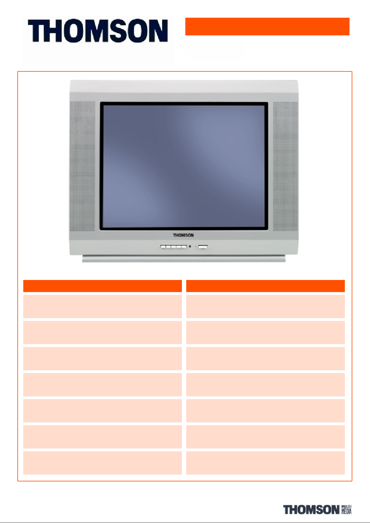
29" Extra-Plat
CARACTERISTIQUES BENEFICES CONSOMMATEURS
Tube X-Flat Focus Gun Choisissez Thomson "Focus Gun" pour des images
pures, lumineuses et contrastées, ce TV propose le
meilleur rapport qualité/pureté d'image - prix
Menu OSD 17 langues Européanisez votre TV en choisissant parmi les 17
langues disponibles dans le menu
2 prises Péritel Possibilité de brancher deux appareils en même temps
(VCR, DVD,...)
Finition spécifique Design conçu pour une meilleure intégration à votre
intérieur (finition argentée, touches couleur chrome, etc...)
Page 2
29 DM 182 T
Données Techniques :
MARQUE Enceinte externe -
Marque THOMSON Prise téléphone pour TAK -
IMAGE Mode VGA -
Taille d'écran : diagonale (cm / pouce) 72 / 29 Connectique Hôtel -
Taille d'image : diagonale (cm / pouce) 68 / 27 CONNECTIQUE EN FACADE
Catégorie 4/3 Entrée CINCH 2 audio / 1 video
Type de tube Extra-Plat Entrée S-vidéo Oui
Masque du tube Invar Prise casque (mm) 3.5
Fréquence 50 Hz DESIGN
Réduction du bruit - Couleur Silver
Contraste image Perfect contrast 2 Couleur cadre Clip'on -
Optimisation du contraste - DONNEES GENERALES
Contrôle du format Oui Code EAN 3244480191743
Transition en zoom - Châssis ETC010
Autoformat 16/9 (plus de bandes noires) - Voltage : secteur 220 - 240 V +/- 10% / 50 Hz
Traitement de l'image - Dimensions Produit (L x H x P) en mm 727 x 567 x 495
Traitement de l'image - Dimensions Emballage (L x H x P) en mm 812 x 655 x 595
Type de zoom - Poids : net / emballé en kg 46 / 41
Type de zoom (2) - Notice d'utilisation : langues (1) D,F,I,GB,GR,DK,NL,S,E,P
Type de zoom (3) - Notice d'utilisation : langues (2) CZ,H,PL,RU,SK,Fi
Multi-image - Consommation en marche / en veille TBD
Préréglages image Personnel / Standard Consommation annuelle (KWh) -
Préréglages image (2) Film/Sport/Studio ACCESSOIRES EN OPTION
Préréglages image (3) - Meuble STTM290
SON Enceintes externes -
Type de son Stéréo Nicam
Puissance musicale (Watt) 2 x 20
Enceintes intégrées (T/M/B) 0 / 2 / 0
Enceintes surround (T/M/B) -
Système Dolby -
Surround sans fil -
Effets sonores spéciaux WIDE / AVL
Technologie des enceintes Dynamic Bass
Préréglages son Ma musique
Préréglages son (2) Film / voix / plat / standard
Préréglages son (3) -
Contrôle du son Egaliseur graphique
Réglage du volume casque Lié au téléviseur
RECEPTION
Norme de réception Pan Européen (LL'/BG/I/DKK')
Standard vidéo (PAL / SECAM) Oui / Oui
Standard vidéo NTSC NTSC 3.58 / 4.43 (AV)
Standard vidéo Pal 60Hz (AV)
Nombre de programmes 99 + AV(s)
Synthèse du tuner PLL
FONCTIONS UTILISATEUR
Arrêt programmable / fonction réveil Oui / Oui
Contrôle parental Verrouillage enfant
Mise en veille automatique Oui
Menu sur écran Navilight
Menu : langues D/F/GB/I/E/P/NL/DK/S/N/FIN
Menu : langues (2) N/FI/PL/CZ/H/SK/RU/GR
Menu languages (3) TR/UK/RO/BG/SL/ET/HR/SR/LT
Nombre de boutons TV 6
Installation Autoprogrammation
Télécommande TV
Clavier sans fil (pour TAK) -
Mode Hôtel Oui
Référence Télécommande RC111TA1G
Alimentation 12 - 24 V -
Jeux /Note calendar/radio FM-RDS - / - / -
SERVICES
Guide TV -
Enregistrement vidéo simplifié -
Type de télétexte 1.5 /Fastext
Nombre de pages télétexte 10
TAK -
CONNECTIQUE ARRIERE
Antenne 1
Péritel 1 CVBS / RVB
Péritel 2 CVBS / S-VIDEO
Péritel 3 -
Entrée / Sortie CINCH audio -
Entrée / Sortie CINCH video -
Entrée / Sortie S-vidéo -
Page 3

ETC009 - ETC010
First issue 01 / 06
SERVICE-MODE - ALIGNMENT PROCEDURE
I - ENTER/EXIT SERVICE MODE
EN
1.1. Accessing Service Mode
A) Switch the TV set into the Standby Mode.
B) Switch off Power Supply.
C) Switch on Power supply whilst pressing the magenta ”TEXT”
key continuously until TV set switch on and enter service mode.
1.2. Page selecting
Press 1,2....8 or 9 key of the RCU to enter page 1,2,...8 or 9 of
Service Mode.
U03C00C 1.8 2005. 07 . 20-01
ADR0 01111010 ADR1 01010000
ADR2 10000010 ADR3 00011110
AFC 00000000 RG 00110111
GG 10110111 BG 00110111
DEFL 00001111 DISC 128
LAST NV : 1878
ERR: 00000000
REV: 882204
1.3. Navigation:
- Press ”Up” and ”Down” key to select option;
- Press ”Left ” and ”Right ” key to adjust or select option.
- All change in service mode will be saved in EEPROM automatically
1.4 Temporary exit from Service Mode
- Press ”9” key and select MODE 1.
- Set D-MODE to ”Direct key enter enable” .
- Press ”OK” KEY on the RC to exit or access to service menu.
1.5. Exiting from Service Mode
- Press ”OK” KEY on the RC.
Note : Before exiting from Service mode check that D-MODE is set to ”Direct key enter disable” (see 1.4).
1.6. Brief introduction on some special modes
1.6.1. Aging Mode
It is used before set alignment and should operate in Service mode;
The TV set cannot enter standby after 15 minutes when no signal if the ”AGING” Mode is selected.
Press blue ”GUIDE” Key, the Aging Mode will be entered when ”Aging Mode” is shown on screen.
Press blue ”GUIDE” key again will exit ” Aging Mode ”.
1.6.2. Vertical Stop mode
- it is used to adjust the screen voltage.
Press red ”PRESETS” key and repress ”PRESETS” (red) key to exit.
1.6.3. White balance alignment mode
- Press ”EXIT” key on factory RCU, The set will display ” BUS OPEN ”, which means the I2C bus from the CPU to
other UOC3 module and ICs had been released. This is only used during automatic adjustment of white balance.
Press other key will exit ” BUS OPEN ”.
1.6.4. Reset
- Initialization before the set will took away from factory.
In factory mode, press ”INFO” (P<P) key, then "RESET" will be shown.
Press "ZOOM+", "BUSY" will be shown.
Initialization will be finished until "BUSY" disappear.
II . FLOW OF ALIGNMENT PROCEDURE
1) B+ Adjustment
2) RF AGC Adjustment
3) Crystal Oscillator Frequency Adjustment
4) Screen & Focus adjustment
5) Sub-color adjustment
6) White balance adjustment
7) Sub-brightness adjustment
8) Picture Geometric adjustment
9) Reset TV set
Page 4
ETC009 - ETC010
First issue 01 / 06
Notes: - Alignment should be done after 3 minutes warm up of TV .
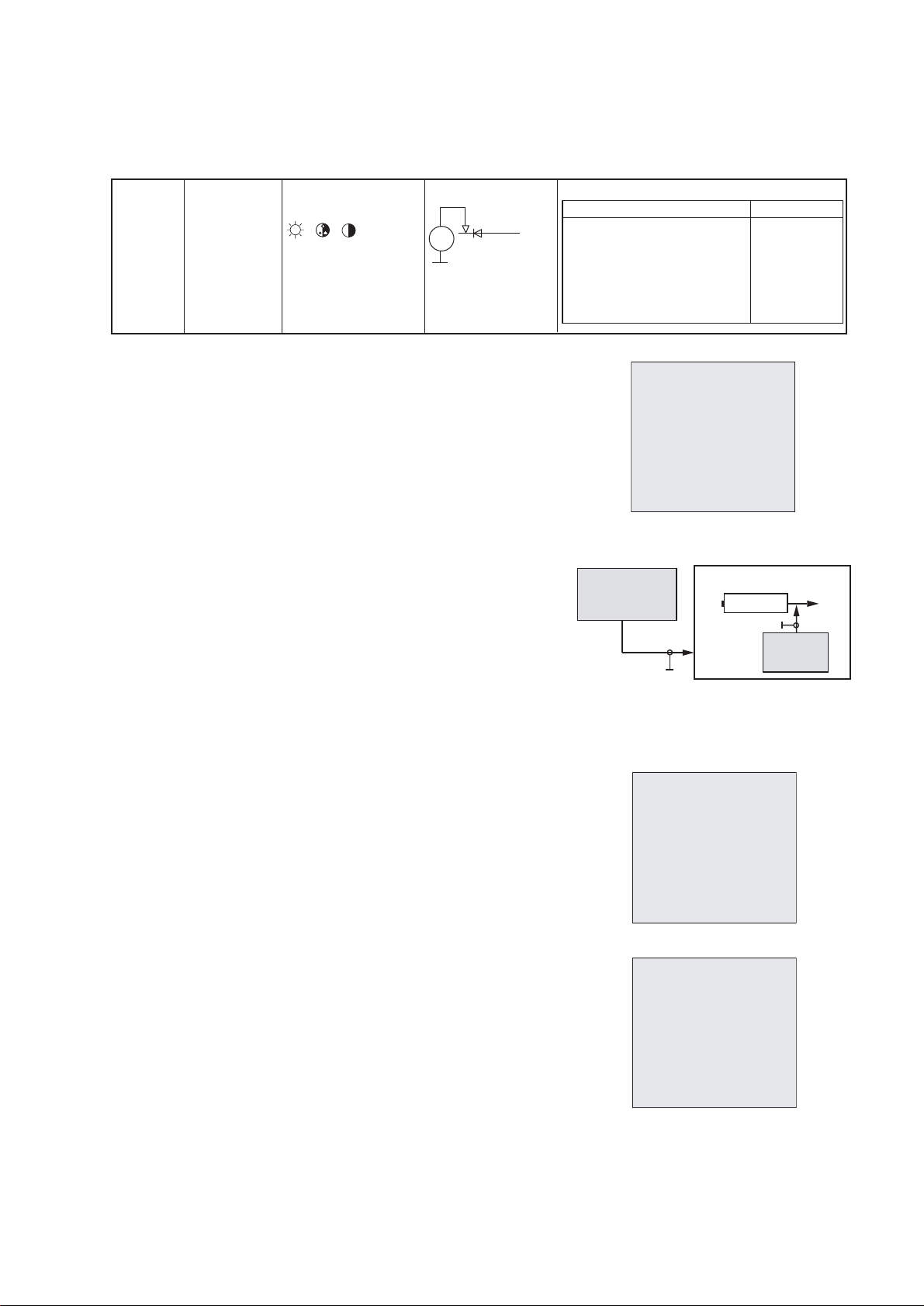
3.1. B+ VOLTAGES
3.2. RF AGC
3.2.1. Method 1
1) Input 60dB PAL BG , with half-Color Bar signal
2) Press key "2" to enter page 2 of factory mode (Fig.1)
3) Select RF AGC with " up " or " down " key. .
4) Press "ZOOM- "(left) and " ZOOM+ " (light) key
until the hint display just change from "Inactive" to
"active".)
5) Adjust AGCL for SECAM L /L' same as the PAL.
3.2.2. Method 2
1) Apply RF signal of 210.25MHz (BG CH 10) modulated
with color bar at 3mVrmx to Tuner input
2) Tune to CH10
3) Go to factory mode, entry page 2 (Fig.1) & set
"RF AGC" to 00 (max IF output).
4) Monitor 38.9MHz IF frequency response at Tuner
pin11 with spectrum analyzer by using high impedance
probe or equivalent.
5) Increase RF AGC control until IF frequency response
8 +1/-2 d B down from maximum.
3.3. CRYSTAL OSCILLATOR FREQUENCY
Notes: - If TV had NICAM function, we recommend to adjust crystal with NICAM.
3.3.1. Crystal oscillator frequency adjustment with NICAM
a) Apply PAL BG NICAM signal with good reception quality.
b) Enter factory mode, press "Vol -"(FORMAT) key ,
it will display " DCXOAUTO " , (Fig.2) then press "ZOOM+" (light)
key to start auto adjust , when it displays "DCXOAUTO OK" ,
the adjust is finished .
3.3.2. Crystal oscillator frequency adjustment without NICAM
( for software with UOC3 TDA12070/12072 only )
a) Input PAL color bar signal.
b) Enter factory mode, press "Vol -"(FORMAT) key ,
it will display " DCXOAUTO " , then press "ZOOM+"
(light) key to start auto adjust , when it displays "DCXOAUTO OK" ,
the adjust is finished .
3.3.3. Crystal oscillator frequency adjustment without NICAM
a) Input PAL color bar signal.
b) In factory mode, press "0" to entry page 0 , (Fig.3).
Adjust "DCXO CAP" until display " DISC " is steady at 128.
III - ALIGNMENT PROCEDURE
V=
B+ Voltage
ETC009: VR801
ETC010: -
(no alignment)
Standard TV - Settings :
TV to AV1 : Black test
pattern
DP805 (ETC010)
DP824 (ETC009)
+
=50%
+
IRICO A36CPAA 00X02 108V +/- 0.5V
TTD A51ELD 032X004 112V +/- 0.5V
LGPD A51ERS 357X440 (SLIM)
ZHONGHUA CHA34AGT13X53 108V +/- 0.5V
TTD ELM021X001 130V +/- 1.5V
TTD W76ELC011X001 132.5V +/- 1.5V
CRT type
B+ Voltage
U0C300C 1 . 8 2005. 07 . 20-01
5VPOS 24
5VAM 29
5VSL 38
5VL 30
5VSC 31
5VSCL 34
RF AGC 14 Active
AGCL 14
Fig.1
U0C300C 1 . 8 2005. 07 . 20-01
DCXOAUTO
Fig.2
U0C300C 1 . 8 2005. 07 . 20-01
YDFE PAL 15
DEC LVL 2
MONO LVL 0
NIC LVL 0
SAP LVL 0
SAP LVL 0
ADC LVL 27
DCX0 CAP 56 DISC: 128
PSCALE 0.375 DCX0:61
PLIM 96
PCENTER 12
LOUDNESS 3
DUB100Hz 6
page 0
page 2
Fig.3
210.25 MHz
3mV
antenna
input
chassis ETC009/ETC010
Tuner
BG CH 10
Monitor IF
38.9 MHz
11
IF
Page 5
ETC009 - ETC010
First issue 01 / 06
Notes: - Alignment below should be done after 15 minutes warm up of TV.
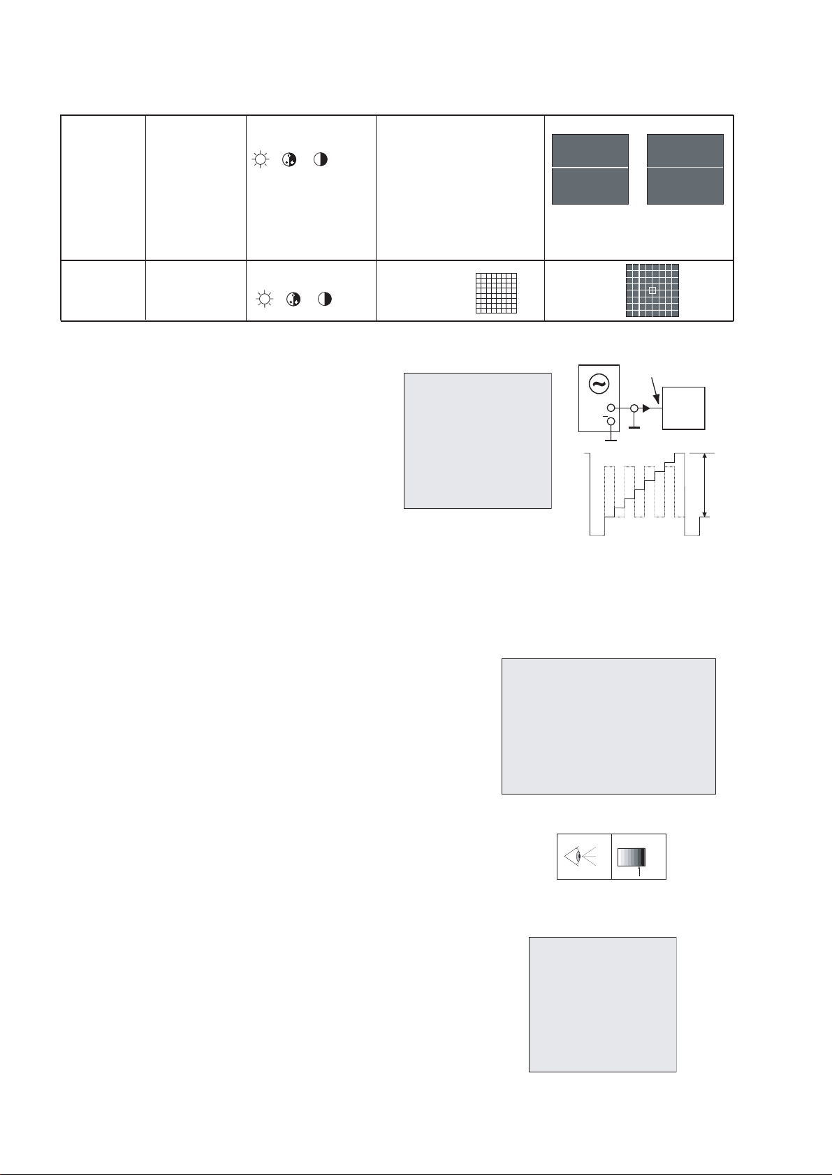
3.4. G2 & FOCUS
3.5. SUB COLOR
a) Input NTSC Video pattern : AV
b) Press key "4" : page 4. (Fig.4).
Measure at the CRT blue Cathode (Fig.5).
c) Adjust COLC to make level a and d equal;
then TNTC to make level b and c equal;
d) Input PAL color bar signal.
e) Adjust COLP to make level of a,b,c,d equal ;
f) Input SECAM color bar signal, and adjust
COLS to make level of a,b,c,d equal.
3.6. WHITE BALANCE
White Balance adjustment (neutral)
a) Input RF Black and White pattern signal (PAL).
b) Press "1" key to enter white balance adjustment (Page 1:Fig.6)
c) Measure the dark side of the picture with a color analyzer.
Adjust RED and GRN until the data on the analyzer
become x=284 +/-8, y=299 +/-8.
d) Measure the bright side of the picture.
Adjust WPR, WPG and WPB until the data on the analyzer
become x=284 +/-8, y=299 +/-8.
e) Repeat step c and d until you get right white balance
on both dark and bright side of the screen.
f) Input RGB Black and White pattern signal (PAL).
g) Measure the dark side of the picture with a color analyzer.
Adjust REDC and GRNC until the data on the
analyzer become x=284 +/-8, y=299 +/-8.
h) Measure the bright side of the picture.
Adjust WPRC and WPGC and WPBC until the data on the
analyzer become x=284 +/-8, y=299 +/-8.
i) Input SECAM L Black and White pattern signal.
j) Measure the dark side of picture with a color analyzer,
Adjust REDSECAM and GRNSECAM until the data on
the analyzer become x=284 +/-8, y=299 +/-8.
Warm color temperature
a) Press green " LIST" key .
b) item: Warm R ; Warm G ; Warm B : Factory adjust
c) Check the item values are as shown opposite.
Alignment of Cool color temperature
a) Press green " LIST" key.
b) item: Cool R ; Cool G ; Cool B : : Factory adjust
c) Check the item values are as shown opposite.
U0C300C 1 . 8 2005. 07 . 20-01
VOL 01 30
VOL 10 104
VOL 90 170
VOL 100 188
CNTC 31
BRTC 30
COLC 23
TNTC 35
COLP 3
COLS 23
SHPTV 32
Fig.4
page 4
Blue
Cathode
CRT
abcd
A
Fig.5
U0C300C 1 . 8 2005. 07 . 20-01
WPR 26 GRNC 40
WPG 29 WPRC 18
RED 31 WPB 31 WPGC 18
GRN 29 REDC 32 WPBC 15
Fig.6
page 1
grey
U0C300C 1 . 8 2005. 07 . 20-01
Warm R 10
Warm G 10
Warm B 10
Cool R 10
Cool G 10
Cool B 10
U G2
Screen voltage
adjustment
G2 potentiometer :
SCREEN
Focus-Block
Standard TV - Settings :
++ = 50%
TV to AV1 : Black test
pattern
1- Press red "PRESETS" (Led)
Key on the remote control
and the screen will become a
horizontal line,
2- adjust the "screen voltage"
of the fly back transformer
until the horizontal line can
just be seen barely
(minimum visible intensity).
No correct Correct :
minimum visible
intensity
FOCUS
FOCUS
VR
Focus-Block
Standard TV - Settings :
++ = 50%
TV to AV1
Test pattern
Sharp picture
Page 6
ETC009 - ETC010
First issue 01 / 06
3.7. SUB BRIGHTNESS
3.7.1. Sub brightness adjustment
1) Input eight steps gray signal.
2) Press key "4" to enter sub-brightness adjustment.
3) Adjust "BRTC" until the secondary gray bar just to be seen.(Fig.7).
U0C300C 1 . 8 2005. 07 . 20-01
VOL 01 30
VOL 10 104
VOL 90 170
VOL 100 188
CNTC 31
BRTC 30
COLC 23
TNTC 35
COLP 3
COLS 23
SHPTV 32
The 2nd gray scale
page 4
3.8 PICTURE GEOMETRY ADJUSTMENT
3.8.1. Vertical geometry items
- Press key "2" to enter Vertical geometry adjustment.
VERTICAL GEOMETRY ITEMS
U0C300C 1 . 8 2005. 07 . 20-01
5VPOS 24
5VAM 29
5VSL 38
5VL 30
5VSC 31
5VSCL 34
RF AGC 14 Active
AGCL 14
5VSL
(V-Slope)
5VAM
(V-Amplitude)
Fig.7
(V-Linearity)
(Vertical
S-Correction)
5VL
5SCL
S
5VPOS
page 2
(V-Position)
*
According to Software
3.8.2. Horizontal geometry items
- Press key "3" to enter Horizontal geometry adjustment.
U0C300C 1 . 8 2005. 07 . 20-01
5HSH 36
5PAR 24
5BOW 22
5EWW 33
5EWP 35
5UCR 42
5LCR 32
5EWT 36
5WBR 7
5WBF 7
page 3
5HSH*
(H-Position)
5PAR*
(Parallelogram)
5BOW*
(Bow Adjust.)
5EWW
(H-Amplitude)
5EWP
(Pincushion
correct.)
5VX*
(Vertical
Over scan)
HORIZONTAL GEOMETRY ITEMS
5UCR
(EW-Upper
Corner)
5LCR
(EW-Lower
Corner)
5EWT
(EW -
Trapezium)
5WBR**
5WBF**
End of
Blanking
Start of
Blanking
Only valid for ETC009 except models with Slim CRT
*
** Only valid with 16:9 tubes
Page 7
ETC009 - ETC010
First issue 01 / 06
3.8.3. Adjustments
Signal : 4/3 test pattern - Cross hatch pattern (PAL or SECAM), NTSC signal to adjust NTSC geometry.
4/3 picture tube
4 / 3
standard mode
Overscan V=107% , H=107%
Vertical adjustment : press ”2”
1- Check the Factory adjust 5VSC = 31; Adjust Vertical Slope : 5VSL
2- Adjust Vertical Position (5VPOS) , Vertical amplitude (5VAM).
3- Adjust Vertical Linearity (5VL) and S correction
S
Horizontal adjustment : press ”3”
1- Adjust Horizontal Position (5HSH) and Horizontal parallelogram (5PAR),
2 -Adjust Horizontal Bow (5BOW)
3 -Adjust Horizontal width (5EWW) and Pincushion correction (5LCR)
4 -Adjust EW Amplitude (5EWP) , EW Upper (5UCR) / Lower Corner (5LCR)
5 -Adjust Trapezium correction (5EWT)
16/9 picture tube
Overscan V=107% , H=107%
Vertical adjustment : press ”2”
1- Check the Factory adjust 5VSC = 31; Adjust Vertical Slope : 5VSL
2- Adjust Vertical Position (5VPOS) , Vertical amplitude (5VAM).
3- Adjust Vertical Linearity (5VL) and S correction
S
Horizontal adjustment : press ”3”
1- Adjust Horizontal Position (5HSH) and Horizontal parallelogram (5PAR),
2 -Adjust Horizontal Bow (5BOW)
3 -Adjust Horizontal width (5EWW) and Pincushion correction (5LCR)
4 -Adjust EW Amplitude (5EWP) , EW Upper (5UCR) / Lower Corner (5LCR)
5 -Adjust Trapezium correction (5EWT)
16 / 9
standard mode
4 / 3 centered
Overscan V=107% , H=77%
1 - Check the 16 / 9 standard mode geometry.
2 - Adjust H. width 77% (5EWW) and pincushion correction (5LCR)
3 - Adjust if necessary lower/upper corner (5UCR/5LCR)
4 - Adjust if necessary the Bow correction (5BOW) and parallelogram (5PAR).
0,8MHz
0%
20%
1,8MHz
100%
3,8MHz
2,8MHz
40%
60%
80%
4,8MHz
5 - Adjust 5WBF 4/3 and 5WBR 4/3to make the castellation just un-visible.
14 / 9
Overscan V=122% , H=90%
0,8MHz
0%
20%
1,8MHz
100%
3,8MHz
2,8MHz
40%
60%
80%
4,8MHz
1 - Check the 16 / 9 standard mode geometry.
2 - Adjust H. width 90% (5EWW) and pincushion correction (5LCR)
3 - Adjust if necessary lower/upper corner (5UCR/5LCR)
4 - Adjust if necessary the Bow correction (5BOW) and parallelogram (5PAR).
5 - Adjust 5WBF 14/9 and 5WBR 14/9 to make the castellation just un-visible.
3.9 RESET TV
When all item alignment is finished, please make the TV to RESET as 1.4.4.
Correct
No correct
Correct
No correct
Page 8
ETC009 - ETC010
First issue 01 / 06
IV - FACTORY ALIGNMENT VALUES
V - SERVICE MODE VALUES
5.1 Analog control adjustment
Press key "5" to enter analog adjustment.
KEY 1 KEY 2 KEY 3 KEY 4
Item Data Item Data Item Data Item
Data
RED 32 5VPOS 32 5HSH 42 VOL 01
30
GRN 32 5VAM 23 5PAR 33 VOL 10
104
WPR 32 5VSL 28 5BOW 29 VOL 90
170
188( ETC009 5W)
194(ETC010 6W)
WPB 32 5VL 30 5EWW 39 VOL 100
176(ETC010,10W)
31(ETC009)
21( for 14”15”)
WPG 32 5VSC **31 5EWP 34 CNTC
31(ETC010)
REDC 32 5SCL 31 5UCR 46 BRTC
30
GRNC 32 RF AGC 22 5LCR 43 COLC
23
WPRC 32 5EWT 26 TNTC
35
WPGC 32 5WBR 7 COLP
3
WPBC 32
AGCL 22
5WBF 7 COLS
23
REDSECAM 32 SHPTV
32
GRNSECAM 32
No adjustable
KEY 5
Data
Item
ETC009 ETC010
CNTX Max. Contrast value 63
13
63
CNTN Min. Contrast value
BRTX Max. Brightness value 63 63
BRTN Min. Brightness value 15 15
COLX Max. Color value 50 50
00
00
00
COLN Min. Color value
TNTX Max. Tint value 63 63
TNTN Min. Tint value
SHPX Max. Sharpness value 63 63
SHPN Min. Sharpness value
5.2 - Picture item adjustment
Press key "6" to enter analog adjustment.
Item
Data
ETC009 ETC010
CPFK PAL Peaking value
NTS peaking frequency & value
32 32
CFPEK PAL PAL peaking frequency & value 3.5M 143NS 3.5M 143NS
CFPEK NTS 3.1M 160NS 3.1M 160NS
CFPEK YUV YUV peaking frequency & value 4.0M 125NS 4.0M 125NS
IFPL IF Offset 32 32
BBTC Base-band tint control (phase U,V signal) 32 32
PGR Original value of R 55 55
PGG Original value of G 55 55
PGB Original value of B 55 55
0
ON
VAM (depends on tube) 3 ( depends on tube)
VG2BRI Brightness of V line when adjust G2 20 20
3 4
HDOL RGB drive gain.
5.3 - OSD Position adjustment
` Press key "7" to enter analog adjustment.
Item
Data
OSD BRI OSD brightness 8
CC BRI Teletext brightness 5
5CCD H Position for Teletext 11
5CCD V Position for Teletext 40
5OSD H OSD H position 9
5OSD V OSD V position 32
5MENU V Menu V. position 55
10
5MENU H Menu H. position
Page 9
ETC009 - ETC010
First issue 01 / 06
5.4 - Option adjustment
Press key "8" to enter Option adjustment.
Check the bytes values. They indicate the configuration of the chassis and are given for information only.
The default values are indicated in the follow table.
- Choose the item Op01 ,Op02 ... by pressing up/down key.
- Access to the selected Option adjustments by pressing ”Left” or ”Right” key
OP01
Fig.8
OP01 : default value : 00001110
Bit 0 - Bit 1: FMWS0/1 (Band width FM; 10: 450kHz)
Bit 2 : AGN (Audio output amplitude; 1: +6dB gain)
Bit 3-Bit 4 : AGC0/1 (AGC time content selection; 01: Normal)
Bit 5 : AVLM (Gain for analog FM decoder; 0: Normal gain)
Bit 6 : CMCA (stereo/mono- 0: stereo 1: mono)
Bit 7 : MAT (Y,U,V to RGB matrix selection - 0:adapted to standard).
OP02
OP02 : default value : 10000100
Bit 0 : MUS (Y,U,V to RGB matrix selection).
Bit 1 : CB
(Select. for center of chroma band; 0: Fsc
)
Bit 2-Bit 3 : CHSE0/1 (Sensivity of color killer; 01: -37dB)
Bit 4 : CL0 (center frequency of SECAM bell filter; 0: 4.29MHz)
Bit 5 :
DTR (Dual Chroma trap; 0: single chroma trap)
.
Bit 6 : SDC (Hor. drive pulse width; 0: Duty cycle 55:45).
Bit 7 : HC0 (EHT tracking only vertical or vertical and EW).
OP03
U0C300C 1 . 8 2005. 07 . 20-01
MVK Macro vision key active
FBC off with fix beam current
EVB Norman vertical blanking
SLG 280uA
ACL Not active
IFS Normal
GD L I No group correction
OP03 : default value : 00010011
Bit 0 : MVK (Macro Vision Keying; 1: active).
Bit 1 : FBC
(switch-off with blanked RGB outputs or fixed beam current
)
Bit 2 : EVB (normal Vert. picture or extended vertical blanking)
Bit 3-Bit 4 : SLG0-SLG1 (selection of AKB black current; 10: 280uA)
Bit 5 :
ACL (control the ratio of chroma/color burst; 0: Not active)
.
Bit 6 : IFS (IF sensitivity; 0: Normal).
Bit 7 :
GDLI (group correction/group delay correction switch for L and I.
0: No group correction).
OP04
U0C300C 1 . 8 2005. 07 . 20-01
FFI Normal time constant
BPB Normal operation
BPB2 bandpass filter
SSL 50%
FSL
dependent on noise detector
No use OFF
OP04 : default value : 00000000
Bit 0 : FFI (IF PLL lock time constant, used for over modulation).
Bit 1 : BPB
(sound bandpass - filter for mono 0: Normal operation
).
Bit 2 : BPB2 (stereo band pass - filter for stereo/dual 0: active).
Bit 3 : SSL (slice level of Hor. syn. Pulse; 0: 50%).
Bit 4 :
ACL
(slice level of Vert. syn. Pulse; 0: dependant on noise
detector).
Bit 5,6,7 : No use
Data
U0C300C 1 . 8 2005. 07 . 20-01
OP01 00001110
OP02 10000100
OP03 00010011
OP04 00000000
OP05 00100111
OP06 00001011
OP07 11000011
OP08 00000000
OP09 00001100
OP010 00110000
Item
OP01 00001110
OP02 10000100
OP03 00010011
OP04 00000000
OP05 00100111 (10100111 for TDA12070/12072/H/N1F00)
OP06 00001011 (00000100 for TDA12070H/N1F00)
OP07 11000011
OP08 00000000
OP09 00001100
OPT010 00110000
Bit 7
00001110
Bit 0
U0C300C 1 . 8 2005. 07 . 20-01
FMWS0/1 450kHz
AGN 6dB
AGC0/1 Normal
AVLM Normal gain
CMCA Stereo mode
MAT Adapted to standard
U0C300C 1 . 8 2005. 07 . 20-01
MUS japanase matrix
CB FSC
CHSE0/1 -37dB
CL0 4.29MHz
DTR single chroma trap
SDC Duty cycle 55:45
HC0
EHT traking on vertical and EW
Page 10

ETC009 - ETC010
First issue 01 / 06
OP05
U0C300C 1 . 8 2005. 07 . 20-01
VAI Amplitude 12%
VA0/VA1 Amplitude +5%
FC0 OFF
VG2 MODE LIGHT LINE
DSS Normal operation
DSG 0dB
OP05 : default value : 00100111
Bit 0 : VAI (gain correction; 0: no correction 1: +12% PAL I).
Bit 1-Bit 2 : VA0/VA1
(IF CVBS output amplitude correction; 10: +5%
).
Bit 3 : OFB (Offset control on Red and Blue channel).
Bit 4 : FCO (force color on when bad signal, color killer not active).
Bit 5 :
VG2 MODE
(0:OSD indication 1:Line).
Bit 6 : DSS (0: normal operation 1: LCD / Pscan
Bit 7 : DSG (audio output selection amplitude; 0: 0dB)
OP06
U0C300C 1 . 8 2005. 07 . 20-01
DCXOMUX Nicam
QSS QSS Amp active
FMI Output conn to QSS0
NICAM ON
RPA0/1 1:1
RP00/1 1:1
OP06 : default value : 00001011
Bit 0 : DCXOMUX (0:P3DCX0 TDA12070/12072/without NICAM
1: NICAM).
Bit 1 : QSS
(validation QSS amplifier; 1: active
).
Bit 2 : FMI (connexion QSS AMP output to SSD module or sound
PLL demodulator; 0: Output conn to QSS0).
Bit 3 : NICAM (NICAM selection; 1: ON)
Bit 4-Bit 5 :
RPA0 /1 (00)
Bit 6-Bit 7 : RPO0/1
(00)
OP07
U0C300C 1 . 8 2005. 07 . 20-01
PWL 3
SOC0/1 0% above PWL
PWL ON PWL circuit active
GD BG DK Group delay correction
OP07 : default value : 11000011
Bit 0-1-2-3 : PWL (peak white limit; default : 3)
Bit 4-Bit 5 : SOC0/1
(% above PW level; 00: 0% above PWL
).
Bit 6 : PWL ON (activation of the peak white limiting circuit; 1: active)
Bit 7 : GD BG DK (activation of the Group delay correction;
0: group correction)
OP08
OP08 : default value : 00000000
Bit : OFF (No use)
OP09
OP09 : default value : 00001100
Bit 0 : AFG (AFC measurement; 0: AFC False)
Bit 1 : TYUV1(Analog output selection for text; valid if TYUV0=1)
Bit 2 : BPBS (Enable bypass of sound filter at stereo mode)
Bit 3 : CLF (Comb filter diode clamp; set to1)
Bit 4 : BWYC (Bandwidth of anti aliasing filter at YC mode of
3.58MHz systems; 0: False)
Bit 5 : CBPS (Internal chroma bandpass filter mode; 0: False)
Bit 6 : SLD (Sleep mode detector status; 0: sleep enabled, False)
Bit 7 : OSB (width of Burstkey; 0: False burstkey=3.52us)
OP10
OP10 : default value : 00110000
Bit 0 : BKC (Internal burst key position; 0: False normal position)
Bit 1 : TYUV0 (TXT/CC output selection; 0: False, RGB format)
Bit 2 : QDT (Q values of Second chroma trap; 0: False)
Bit 3 : FBC1 (Fixed beam current during switch off; 0: False, 1mA)
Bit 4 : TCCON (Top sync. clamp control; 1: True , active)
Bit 5 : TCI2X (Top sync. clamp time constant; 1: True)
Bit 6 : TXTS (TXTS Mode : TEXT source; 0: False TXT from CVBS)
Bit 7 : Blue SCN (Blue screen with no signal; 0: False)
U0C300C 1 . 8 2005. 07 . 20-01
No use OFF
U0C300C 1 . 8 2005. 07 . 20-01
AFG False
TYUV1 False
BPBS True
CLF True
BWYC False
CBPS False
SLD False
OSB False
U0C300C 1 . 8 2005. 07 . 20-01
BKC False
TYUV0 False
QDT False
TCCON True
TCI2X True
TXTS False
Blue SCN False
Page 11

ETC009 - ETC010
First issue 01 / 06
5.5 - Mode adjustment
Press key "9" to enter Mode adjustment.
Check the bytes values. They indicate the configuration of the chassis and are given for information only.
The default values are indicated in the follow table.
- Choose the item MODE 1 ,MODE 2 ... by pressing up/down key.
- Access to the selected MODE adjustments by pressing ”Left” or ”Right” key
MODE 1
U0C300C 1 . 8 2005. 07 . 20-01
D-MODE
Direct Key enter disabled
AV OUT Always TV
NO SIG. Mute when no signal
MUTE AV0
Don't mute AV-Out
NI ADISP OFF
SEARCH Fast
TUNER CP OFF
TXT FIN OFF
MODE1 : default value : 10110100
Bit 0 : D-MODE (Direct enter D-mode (Service mode) with ”OK” key
0:enable 1:disable)
Bit 1 : AV OUT (0: Always TV - 1: Follow source)
Bit 2 : No Signal (0: Demute when no signal - 1 mute when no signal)
Bit 3 : MUTE AV0 (Mute AV-out)
Bit 4 :
NI ADISP (1: Nicam auto detection OSD display enable)
Bit 5 : SEARCH (Auto search speed setting)
Bit 6 : TUNER CP (CP bit selection of tuner)
Bit 7 : TXTFIN (TXT fine tuning selection)
MODE 2
U0C300C 1 . 8 2005. 07 . 20-01
SOUND DK ON
SOUND BG ON
SOUND M OFF
DEF SND
BG
MAX PROG 100 Prog
AUTO SND
Request auto sound
MODE 2 : default value : 10011111
Bit 0 : SOUND DK (depends on requirement)
Bit 1 : SOUND BG (depends on requirement)
Bit 2 : SOUND L (or I)* (depends on requirement)
Bit 3 : SOUND M (or I)* (depends on requirement)
Bit 4 - Bit5 :
DEF SOUND (00: DK; 01: BG; 10: I; 11:M)
Bit 6 : MAX PROG. (0: 100, 1:200 (no used))
Bit 7 : AUTO SND (Request auto sound detect when auto searching
(0: Don’t request 1: request auto sound)
* according models
MODE 3
MODE 3 : default value : 00000000
Bit 0-Bit 1 : DBB/DVB (Woofer 00:DVB; 01:DB; 10: Woofer, 11:OFF)
Bit 2 : AVL (0: OFF)
Bit 3 : Tilt (0: OFF)
Bit 4 : COMB (Comb filter : 0: OFF)
Bit 5 : VM (0:OFF)
Bit 6 : SECAM (0:OFF)
Bit 7 : SUPERREC (0:OFF)
MODE 4
MODE 4 : default value : 11111101
Bit 0-Bit 1 : IF FREQ (00:45.75MHz; 01:38.9MHz; 10: 38MHz)
Bit 2 : AV1 (1:ON) (depends on requirement)
Bit 3 : AV2 (1: ON) (depends on requirement)
Bit 4 : AV3 (1: ON) (depends on requirement)
Bit 5 : S-VIDEO1 (1: ON) (depends on requirement)
Bit 6 : S-VIDEO2 (1: ON) (depends on requirement)
Bit 7 : RGB (1: ON) (depends on requirement)
U0C300C 1 . 8 2005. 07 . 20-01
MODE 1 00110101
MODE 2 10010111
MODE 3 00000000
MODE 4 11111101
MODE 5 11000000
MODE 6 10001100
MODE 7 01110010
MODE 8 00101000
MODE 9 11001000
MODE10 00100000
Item
MODE 1 010110100
MODE 2 10011111 (10011011 for TDA12070/12072 without L standard)
MODE 3 00000000
MODE 4 11111101
MODE 5 01000000
MODE 6 10001100
MODE 7 01110010
MODE 8 00000000
Data
MODE 9 11001000
MODE 10 00110000
Bit 7
00001110
Bit 0
U0C300C 1 . 8 2005. 07 . 20-01
DBB/DVB DVB
AVL OFF
Tilt OFF
COMBFILT OFF
VM OFF
Secam OFF
SuperRec OFF
U0C300C 1 . 8 2005. 07 . 20-01
IF Freq 38.9MHz
AV1 ON
AV2 ON
AV3 ON
S-VIDEO1 ON
S-VIDEO2 ON
RGB ON
Page 12

ETC009 - ETC010
First issue 01 / 06
MODE 5
MODE 5 : default value : 01000000
Bit 0,1,2,3,4 : No use
Bit 5 : Radio (FM Radio 0:OFF)
Bit 6 : EQ BAR (User menu display (0: bass & Treble; 1:Equalizer)
Bit 7 : BCF CHEK (Beam current protection 1:ON)
MODE 6
MODE 6 : default value : 10001100
Bit 0 - Bit 1: Power ON (Power on status 00:ON, 01:standby, 10 last status)
Bit 2 : MUTE PIC (Mute picture when changing channel; 1:ON)
Bit 3 : HCT (High Contrast for OSD; 1:ON)
Bit 4,5,6,7 : DURATION (mute time when changing channel; default 8)
MODE 7
MODE 7 : default value : 01110010
Bit 0 : No use
Bit 1 - Bit 2: X-RAY V (Detection voltage for X-ray protection; 01:1.9V)
Bit 3 - Bit 4: X-RAY T (Detect. time for X-ray protection; 10: 750ms)
Bit 5 : No use
Bit 6 : 4:3 OSVE (selection of vertical over scan; 1:ON)
Bit 7 : DOLBY (selection of DOLBY; 1:ON)
MODE 8
MODE 8 : default value : 00101000
Bit 0-Bit 1 : VMA (Amplitude of SVM output ; 00 : ST OFF)
Bit 2,3,4 : SVM (Delay of RGB to SVM output; 010 : ST 50ns)
Bit 5,6,7 : SPR (Parabola on SVM output; 001 : 0/-3/-3)
MODE 9
MODE 9 : default value : 11001000
Bit 0-Bit 1 : VMA (WEAK status 00: OFF)
Bit 2,3,4 : SVM (WEAK status 010: 50ns)
Bit 5,6,7 : SPR (WEAK status 110: -6/-3/-0)
MODE 10
U0C300C 1 . 8 2005. 07 . 20-01
SVMA 600mVpp
CRA0 8%
TXTLV 0
COFF False
No use OFF
MODE 10 : default value : 00100000
Bit 0 : SVMA (SVM output signal ; 0 : 600mVpp)
Bit 1 : CRA0 ( adjusted to 8% - Bit 1 = 0)
Bit 2,3 : TXTLV (Scavem on TXT ampl.; 10: 1000mVpp)
Bit 4 : COFF ( adjusted to False - Bit 4= 0)
Bit 5,6,7 : No use
U0C300C 1 . 8 2005. 07 . 20-01
RADIO OFF
EQ BAR Equalizer Bar
BCFCHECK ON
U0C300C 1 . 8 2005. 07 . 20-01
POWER ON Power On
MUTE PIC ON
HCT ON
DURATION 8
U0C300C 1 . 8 2005. 07 . 20-01
16:9TUBE OFF
XRAY V 1.9V
XRAY T 750ms
4:3 OSVE ON
DOLBY OFF
U0C300C 1 . 8 2005. 07 . 20-01
VMA ST off
SVM ST 50ns
SPR ST 0/-3/-3
U0C300C 1 . 8 2005. 07 . 20-01
VMA WK off
SVM WK 50ns
SPR WK -6/-3/-0
Page 13

ETC009 - ETC010
First issue 01 / 06
VI - TEXT KEY
Press the ”Text” key and check the item values are as shown below.
KEY TEXT (change item in sound menu / Equalizer)
Data
Item
FL
(Flat)
(Music) (Voice) (Film) (Standard) (Perso..)
MVFSP
BASS 12 24 24 16 16 12
TREBLE
20 24 16 24 16 20
100HZ 676766
300Hz
699896
1KHz
669686
5KHz
689666
8KHz
6976
6
10
Text key menu according to
equalizer presetted in sound
menu: ie ”Standard”
VII - ”PR-” / ”0” KEYS
Press the ”PR-” then ”0” key and check the item values are as shown below.
”PR-” KEY
”0” KEY
U0C300C 1 . 8 2005. 07 . 20-01
BASS S 16
TREBBLE S 16
100Hz S 6
300Hz S 9
1Khz S 8
3Khz S 6
8Khz S 7
U0C300C 1 . 8 2005. 07 . 20-01
SET P1 147MHz
SET P2 423MHz
DATA VL 00000001
DATA VH 00000010
DATA UF 00001000
SPE POS1 00000000
SPE DATA 00000000
SENSI ON 00000000
SENSI OFF 00000000
U0C300C 1 . 8 2005. 07 . 20-01
YDEFE PAL 15
DEC LVL 2
MONO LVL 0
NIC LVL 0
SAP LVL 0
ADC LVL 27
DCX0 CAP 56 DISC:127
PSCALE 0.375 DCX0:56
PLIM 96
PCENTER 12
LOUDNESS 3
DUB100Hz 6
Page 14

ETC009 - ETC010
First issue 01 / 06
BLOCK DIAGRAM - SCHEMA SYNOPTIQUE - BLOCKSCHALTBILD - SCHEMA A BLOCCHI
ESQUEMA DE BLOQUES
ETC010
Power
MAIN
Relay
Suply
TDA16846
LOW B AUDIO VCC
RGB Amp
Pin out
H-drive
H-out
Feed back
AUDIO AMP
TEA2025 (2W )
TDA7266SA(6W )
TDA7297SA(10W )
+B
V-out
STV9380A
Hout
VCC
FBT
L
R
P909
SCART1
P911
SCART2
FSS T UNE R
AGC IN
24.576MHZ
5V 33V
P920
SCART1
OU T
P922
SCART1
IN
P204
SCART1
IN
P921
SCART2
OU T
P200
SIDE A V
SIF
SAW
31 AG C OU T
36 A-OU TSL
37 A-OU TSR
48 SV O
I/O Port
53,54 AI N2L
55 CV BS2/Y 2
78 R/PrIN3
80 B/PbI N3
79 G/Y IN3
116,115 ST1/2
77 FB
49,50 AI N4L /4R
51 CV BS4/Y 4
52 C4
56,57 AI N3L /3R
58 CV BS3/Y 3
59 C2/C 3
10 X T AL IN
11 X T AL OU T
/2 R
PLL
VIF
SAW
VIF & SIF
Color
Decoder
CC & V-chip
I/O Port
97 IR P0.5
Key bu ttons
Micro
Text
120 K EY B
103 LED P0.3
LED
POWER
YUV
Procrssor
109 SDA P1.7
108 SCL P1.6
A
Stereo, DS P
D
C
NVM
Ac in
RGB
RGB OUT 85,87
Jungle
VDRA 23
VDRB 22
SVM 65
E-W 21
AUDIO
OU T
StdbyPower
TEA1520P
Stb P1.1 99
RGB
V+ V-
EW, HD
Page 15

ETC009 - ETC010
First issue 10 / 04
MAIN SCHEMATIC DIAGRAM - SCHEMA DE LA PLATINE PRINCIPALE - SCHALTBILD HAUPTPLATINE - SCHEMA DELLA PIASTRA PRINCIPALE- ESQUEMA DE LA PLATINA PRINCIPAL
( MAIN BOARD 1/4) / ETC010
+3.3VSTB
C082
10n
+5VSTB
C085
10n
STANDBY
RELAY
(V) Standby Mode
+
C083
100uF
IC 806
LD 1117-33B
OIN
(3,3)
5
(5)
3,3
+
C086
100uF
OIN
(7)
6,2
D866
NA
G
G
IC 805
LD 1117-50B
D829
1N5817
R800
100K /1%
R824A
91K /1%
R824B
0
+5V
C090
100u/16V
+5V I F
C092
100u/16V
C867
100n
6,2
(7)
+
0.1u
R824
2K /1%
+
(7)
6,2
R801
1K
C843
1nF
C842
VR 800
NA
(0)
5
+
C868
470u 16V
R825
33K
C091
0.1u/50V
(0)
5
C093
0.1u/50V
L861
100uH
C8 09
NA
+
R802
100
IC 800/1/2
PC123
!
IC 803
TL 431
IC 804
LD 1117-50B
OIN
G
D090
5.1V
+
C866
1000u/ 16V
R851
JUMPER
R893
1K
+33V
D824
JUMP ER
R091
100
C865
1000P
+130V
+6.5V
6,4
C869
NA
D868
UF 4004
P800
R817
22K 1W
C848
1000p/16V
(0)
VR 803
NA
12
SW800
P801
P802
3
2
1
+13V
!
POWE R SW
+
C850
10u/16V
R892
1.5K
1000uF/25V
L8 04
100uH
+
3
2
1
D850
4148
Q850
C1815
(11,3)
C817
RU4 YX
0.1u
13,2
+
C8 15
!
C880
10U/50V
L8 00
100uH
R877
NA
C846
2200uF/16V C8 56
C8 45
220u/16V
C894
102P
C814
220u/160V
+
!
C847
100n
129,5
(0)
6,5
3
2
1
5V REL AY
D806
220P/500V
(0)
!
+
D825
SR360
C849
220P/500V
12
VR 804
!
F800
3.15A/250V
K851
R884
FUS E/5A
!
C8 21
C820
220P
C8 18
0.01u/500V
R883
FUS E/3A
471V
!
0.22uF/275V
!
4148/NA
D805
MVR 46 0
Z801
NA
C813
!
R813
1M
+6.5V
100u/16V /N A
D85 2
L813
NA
L812
BF -35050C
L810
BF -35050C
L811
BF -35050C
C851
1
T800
LI F002
+
R853
4.7K/N A
R852
27K/NA
18
16
17
10
11
12
15
14
102P/400VAC
0.22u/275V
!
D851
4148/NA
T801
C882
R882
8M2
C822
!
Q851
1815/NA
1
5
9
8
7
C835A
470P/400V AC
!
C828A
470P/400V AC
J803A/N A
J803
!
K850
5V REL AY /N A
R814
47
C826
47uf/25V
R834
22K
!
C825
68n
1H8
D810
D811
IN 4148
RT 800
9OH M
+
C858
330P
T802
LI F001
400V /100n
56K /5W
R816
C827
220P
R833
1M
P803
C823
t
o
12,6
C830
1,9
0.1u
R840
1K
33K
R838
5
T860
3
(153)
269
C890
100P/1K V
C860
10n 500V
R861 75K
D860
1H8
R862
2.2 1/4W
D865
FR 102
R860
1M
1/4W
8
7
6
5
IC 860
R865
120
D
NC
TE A1520P
S
AU X
+
C893
1u 50V
VC C
GND
REG
RC
(-118)
-3,2
1
2
3
4
(-128,6)
-11,7
C864
0.1uF/63V
(-129)
-12,5
R868
30K
C861
4.7u 400V
D867
7.5K/1/4W
R864
5.1K
+
C8 62
100n
C863
470p
6
2
10
1
!
1
2
14
R863
9.1K
!
C8 54
1500P
C835
4n7/250VAC
4
C8 28
4n7/250VAC
!
C824
10n/500V
L8 02
LB 1005
C836
560P
R811
4M7
(0,5)
R816A
3,9
471K
4,6
13
12
IC 802
TDA 16846
234
1,3
(0)
10n
R830
C8 55
8.2K
300P
L860
(152)
5OH M
267
11
1
!
3
+
C8 29
220u/400V
Q805
A 04N80
R818
56K
10
5,5
(0)
D862
1N4007
DB80 1
D3SB60
274
!
(0)
3,7
!
R822
220
R823
1K
(0)
C833
0,6
2200P
9
5
6
2,9
(0)
C8 57
10n
!
D86 4
1N4007
C891
1500P/250VAC
D861
1N4007
D86 3
1N4007
C892
MAIN
2
!
D8 21
IN 4148
8
71
R819
D828
9.1V
R823A
47
C841
220P
11K
(0)
5,5
IC801/1/2
PC123
R821
4.7OHM
C837
100n
C8 38
1n
Note :
Power Supply primary circuit measurements.
- Use only ( ) connection point.
Attention :
Mesure dans la partie primaire de l'alimentation
- Utiliser la masse du bloc alimentation ( ).
Achtung :
Bei Messungen im Primärnetzteil
- Primärnetzteilmasse verwenden ( ).
Attenzione :
misure nell'alimentatore primario
- usare massa alimentazione primario ( ).
Cuidado :
Medida en el bloque de alimentacion
- Utilizar la masa del bloque de alimentacion ( ).
Part of board connected to mains supply.
Partie du châssis reliée au secteur.
Primärseite des Netzteils.
Parte dello telaio collegata alla rete.
Parte del chasis conectada a la red.
Use isolating mains transformer
Utiliser un transformateur isolateur du secteur
!
Einen Trenntrafo verwenden
Utilizzare un transformatore per isolarvi dalla rete
Utilizar un transformador aislador de red
!
Indicates critical safety components, and identical components should be used
for replacement. Only then can the operational safety be garanteed.
Le remplacement des éléments de sécurité (repérés avec le symbole ) par
!
des composants non homologués selon la Norme CEI 65 entraine la non-conformité
de l'appareil. Dans ce cas, la responsabilité dufabricant n'est plus engagée.
Wenn Sicherheitsteile (mit dem Symbol gekennzeichnet) durch nicht
!
normgerechte Teile ersetzt werden, erlischt die Haftung des Herstellers.
La sostituzione degli elementi di sicurezza (marcati con il segno ) con
!
componenenti non omologati secondo la norma CEI 65 comporta la non conformitá
dell'apparecchio. In tal caso é “esclusa la responsabilità” del costruttore.
La subtitución de elementos de seguridad (marcados con el simbolo ) por
!
componentes no homologados segun la norma CEI 65, provoca la no
conformidad del aparato. En ese caso, el fabricante cesa de ser responsable.
Power supply
Q805 (D) Ch1 Pk-Pk 756V
1
Ch1 200V Period 21,39µs
M 20.0 µs
Power supply
IC860 Pin 8 Ch1 Pk-Pk 524V
1
Ch1 200V Period 4,524µs
M 10.0 µs
Power supply
Joint Of L810&C820 Ch1 Pk-Pk 32,8V
1
Ch1 10V Period 18,52µs
M 10.0 µs
Power supply
Joint Of L811 / R833 Ch1 Pk-Pk 2,18V
1
Ch1 500mV Period 16,24µs
M 10.0 µs
Page 16

ETC009 - ETC010
First issue 01 / 06
MAIN SCHEMATIC DIAGRAM - SCHEMA DE LA PLATINE PRINCIPALE - SCHALTBILD HAUPTPLATINE - SCHEMA DELLA PIASTRA PRINCIPALE- ESQUEMA DE LA PLATINA PRINCIPAL
( MAIN BOARD 2/4) / ETC010
SCANNING / DEFLECTION
Vert Deflection (PIN 4 P400)
1
Ch1 2V Period 20ms
M 10.0 ms
SCANNING / DEFLECTION
Horiz Deflection (PIN 2 P400P)
1
Ch1 100V Period 24,12µs
M 20.0 µs
SCANNING / DEFLECTION
Vert Deflection (PIN 3 P400)
1
Ch1 50mV
M 20 ms
SCANNING / DEFLECTION
Vert Deflection (PIN 12 IC301 IN-)
1
Ch1 50mV
M 20 ms
SCANNING / DEFLECTION
Horiz Deflection (PIN 1 P400)
1
Ch1 500V Period 64µs
M 40.0 µs
Ch1 Pk-Pk =7,16V
Ch1 Pk-Pk =240V
Ch1 Pk-Pk =1,3V
Ch1 Pk-Pk =0,5V
Ch1 Pk-Pk =1,2KV
MAIN
ABL
SANDCASE
H-OUT
ROTATION
VDRA
VDRB
E-W
X-RAY
(TO P406)
D419
IN 4148
0.1U/50V
C405
0,4
Q403
BC 846B
R412
10k
7,2
R316
3K 9
R413
820
C351
2200P
4u7/ 50V
C403
390P/500V
0,3
R406
470
R350
3K 9
C300
50V/100uF
D283
C402
+
!
C350
1500P
+
+14V
6.5V
Q402
BC 639
R406
470
R349
6K 2
D304
2V4
IN 4148
D411 IN 4004
D412
1N4004
9,3
D300
4148
D305
4148
2.2K1/4W
R300
1K 2
6.5V
1/2W 15
R411
1000P/500V
R315
3K
D282
R410
1W 27
R409
C404
R351
6K 2
D306 3V 9
+
C307
47uF 25V
!
IN 4148
2,7
D307
4148
D308
4148
!
R282 330
0,2
!
Q281
BC 847A
T401
BCT- 1012B
!
R308
R280
5K 6
!
2K 7
R286
220
R283
-14V
33
!
!
L402
LGA
Q280
C857A
L401
1uH
IC 301
STV9380A
470PF
R307
10K
R304
C314
1000P
56K
R305
5,4
!
0,2
24V
!
D280
Q405
3DD340 2
!
3,1
C4 07
0.01uF
!
IN 4148
R285
470
D408
6.5V
-11
R306
D2 81
11
0,3
sgnd
Freq
10
C334
10n
52K
D310
4148
4,8
!
3300P/1.6KV
D402
FR 104
68K
BZX79C5V 6
R1301
10 2W
R1304
1K
R1307
1K 2
R314 82K
C352
12
0,4 0 13,2
IN-
C353
C308
1000P C354
220uF/25V
13
14
15
EAout
IN+
Feedcap
Vreg
Boot
8
9
0
-3,5
C3 26
0.1UF
7
9,5
100uF 35V
-12,5
C823A
220u/160V
3
2
+
1
P401
C4 10
C408
8200P/1.6KV
D4 01
!
BY 228
L403 LGA 800uH
!
C411
0.022/400V
19,6
R418
R420
3.9/2W
Q407
630MFP
6,3
+
C1301
100u/25V
BC 847A
Q1302
R1306
10K
Q1 301
BC 847A
R1305
470
2200P
+
16
+Vcc
-VccP
CFfly-
Cfly+
6
5
14
+
C323
!
22uF/250V
+130V
!
ZD DF
C413
JUMP
4300P/1.6KV
0.33uF/250V
C414
+
R1302
1K
R1303
470
1uF/50V
C1303
1uF/50V
+14V -14V
100nF
-13,9
17
18
-VccP
-Vcc
-Vcc
out
3
4
0
C327
0.22
C401
+200V
220P500V
C400
+
D400
FR 104MF
R432
D413
10K
5V1
L404
4.7mH
R402
68 2W
-14V
C416
1000uF/35V
+14V
!
C415
1000uF/35V
Q1303
C1815
+
C1302
Q1304
A1015
+
Q1306
A1015
19
-Vcc
-Vcc
2
C420
R284
56K
6,3
Q1 305
C1815
-14V
220P
+
C309
220uF/25V
20
-Vcc
-Vcc
C328
820PF
1
R422
FU S
FU S
R423
3.9K
R424
R425
4.7K
+
4u7/50V
R287
39K
220P 500V
!
+
D405
FR 104MF
D404 FR105
+
C418
220P 500V
+
C1304
2.2u/50V
10NF
C355
1 1W
1 2W
C417
C419
1
2
P1301
FR 104MF
L301
1MH LC-EE 1941-TCL
-
14V
R313
3K 3C325
D406
R427
2W FUS 4.7
R426
2W FUS 4.7
C421
100n
E
-
C360
+
1uF
1
10
2
7
11
8
4
5
-0,6
BC 847A
R320
1/2W 68
R324
0.56
R429
1K
Q408
TRL 242 21uH
1W
T4 02
!
FB T- 3
+14V
R321
330
L4 00
R401
680
R428
6K 8
C422
10n
R323
100 /2W
C357 470n /63v
P400
!
TO CRT
R430
4K 7
R431
4K 7
OP EN
NC
CON4
4
3
2
1
4
3
2
1
P403
=>P503
C337
220n
EH T
FOCUS
A5
SCREEN
R421
AB L
9
1W FUS
P403
6.5V
4148
5,9
D407
LL 4148
D4 10
H-OUT from UOCIII
(Base Q403)
1
Ch1 100mV Period 64µs
M 40.0 µs
Ch1 Pk-Pk =264mV
SCANNING / DEFLECTION
PIN 13 of IC301 (IN+)
1
Ch1 50mV Period 20,86ms
M 10.0 ms
Ch1 Pk-Pk =0,4V
Page 17

ETC009 - ETC010
First issue 10 / 04
MAIN SCHEMATIC DIAGRAM - SCHEMA DE LA PLATINE PRINCIPALE - SCHALTBILD HAUPTPLATINE - SCHEMA DELLA PIASTRA PRINCIPALE- ESQUEMA DE LA PLATINA PRINCIPAL
( MAIN BOARD 3/4) / ETC010
P920
5
4
3
2
1
P922
5
4
3
2
1
P204
7
6
5
4
3
2
1
P204 RGB IN
P920 SCART1 OUT
P921
7
6
5
4
3
2
1
CON7
R
L
V
Y
C
100
R963
1n
R960
C967
1n
R962
C961
Cb
Cr
Y
P904
L915
600 ohm
L913
600 ohm
L902
600 ohm
L905
Vo
L910
600 ohm
SIDE AV
P961
C962
C963
+
100uF
100uF
220
R961
220
C960
3300P
100
REA R YUV INP UT
D905
5V6
D906
5V6
D907
5V6
C936
2n2
C938
2n2
L907
600 ohm
L908
600 ohm
L909
600 ohm
D902
5V6
P964
+
C966
*
C941
330P
600 ohm
P962
CON7
P966
3300P
R943
82
R944
82
R954
82
R914
L912
2.2uH
C939
C943
330P
C944
330P
L914
2.2uH
C937
2n2
2n2
L904
600 ohm
75
D904
5V6
C918
220P
7
6
5
4
3
2
1
1
2
C953
100P
C954
100P
C955
100P
R904
R905
47K
R912
75
L906
600 ohm
2
1
2
3
1
2
3
4
5
R902
330
R903
100k
27K
R911
D900
5V6
7
6
5
4
3
2
1
P967
CON3
P969
CON5
R900
330
75
R923
47K
P200
CON7
R940
100
R941
100
R942
100
R901
100k
C942
R926
C919
220P
100pF
R908
R921
47K
75
D903
5V6
C903
C906
330P
R920
27K
R922
2n2
75
C909
220P
27K
L911
2.2uH
C945
2n2
C902
100pF
R916
C946
C932
220P
D901
C950
100pF
C951
100pF
C952
100pF
Q902
BC 847A
R906
27k
Q900
BC 847
C920
+
1K
1K
C933
220P
R935
75
A5 R
A5 L
C907
2n2
1k
R915
R917
1k
C912
+
2.2uF
C914
+
2.2uF
0.1uF 50V
+
C957
2.2uF
+
C956
2.2uF
C930
2n2
C931
2n2
-1,7
R918
C940
220P
R947
C905
2.2uF
75
1K
R946
1K
C901
10uF
Q903
BC 847A
2,3
R934
75
C908
2.2uF
+
+
AV-MUTE
C904
10uF
0
+
+
+
Q901
BC 857
1,6
C911
0.1uF
MAIN
P9X X
REA R YUV A UDIO INPU T
R
R949
47K
L
R948
47K
ST 1
ST 2
SCL / SDA
SCL (PIN 4 P003)
A
1
Ch1 200mV Period 11,53µs
M 200µs
SCL / SDA
SDA (PIN 2 P003)
1
Ch1 200mV Period 203µs
M 100µs
SVBS
CVBS from scart out (PIN 19)
1
Ch1 50mV Period 223,3ns
M 20µs
P008
SDA2
SCL2
D/A
STB
IRQ
A
Ch1 Pk-Pk =5V
Ch1 Pk-Pk =5V
Ch1 Pk-Pk =1,6V
1
2
3
4
5
6
R270
100
33K
R244
C264
11
XTALOUT
R231
12345
10
100
P202
220K
R245
3.3K
0.022uF
100uF/10V
C223
C221
33pF
Z200
24.576MH z
XTALI N
C255
R232
220nF
R271
18K
100nF
+
C222
8
9
vrefP_Sdac
VrefN_ Sdac
VREF AD_NEG89VREF AD_ POS
+3.3V analog
88BO87GO86RO85
Z217
Z216
100n
L208
10uH
C256
C254
47PF
Q206*
BC 857A
/254
7
90
L201
1uH
L209
10uH
Vref P_Sdac
ABL
+3.3V
6
91
VrefN_ Sdac
VREF AD
C258
100nF
R255
1K
-STB
1uH
L202
Z210
5
4
Vref P_Sdac
TDA12066H
TDA12061H
TDA12011H
TDA12010H
TDA12027H
GNDA
93
92
Z222
+
C257
47uF 25V
L210
1uH
C259
47PF
Q207*
BC 857A
C224
100nF
C226
3
GA ME L P1.5
1.8VC4
3.3VA3
GA ME R P1.4
SCA RT 1 P3.1
SCA RT 2 P3.0
ROTA TION P2.2
TUNING P2.0
IBO D/A P0.1
IBO STB P0.2
TV STB P1.1
VDDA1
VDDA2
94
C260
220nF
3.3V-STB
R256
1K
+5VSTB
C225
+
10uF
L2 13
600 ohm
100nF
1
2
GND
GND
P1.2
GND
1.8V
P2.5
MU TE P2.4
GND
KEYB P3.3
X-RA Y P3.2
DECV1V8
1.8V
P2.3
P2.1
3.3V
SDA P1.7
SCL P1.6
SDA2 P1.3
SCL 2 P0.0
LE D P0.3
P0.4
V SSC2
VDDC 2
IR Q P1.0
IR P0.5
VDD
VS S
96
95
Z218
C261
220nF
C268
47PF
Q208*
BC 857A
R214
10K
R211
10K
C227
10uF
IC 200
TDA 1 2067H
L211
+
C262
47uF
R216
1W 1 ohm
R215
33K
2,5
(0)
+
L203
10uH
128
127
126
125
100nF
C017
124
C019
Z221
123
122
C018
0.01uF
121
120
119
Z220
118
117
C022
220nF
116
R038
100
115
R037
100
114
113
112
111
Z219
110
109
R029
108
R028
107
106
105
R035 100
104
R036 100
103
R050 10k
102
101
100
C028 220nF
99
98
100
97
R034
1uH
P130
1
2
3
4
C130
220P
Somes Models*
R257
1K
+5V
10uF
220nF
4,9
(5)
4,2
Q202
BC 847A
+
C023
3.3K
3.3K
R042
3.3K
100
R021
(0)
1,9
JP130
L001
10uH
(5)
1K
+
10uH
L004
R048
10K
R049
47K
Q203
BC 327
2,5
(0)
100
R024
L003
10uH
C024
47uF
R022
5.6K
R023
+3.3VST B
L002 10uH
R047
10K
R130
220
+5VSTB
22K
R017
10K
R018
C025
3.3K
R027
100
R025
100
R026
100
R041
100
R043
R044
22k
R045
22k
R046
22k
R051
100
C131
220P
R212
33K
Q200
BC 847A
+5VST B
+
2.2uF/50V
+5VST B
R131
220
R213
1W 1 ohm
(5)
4,9
Q201
4,3
BC 327-40
(1,7)
1,9
(V) Standby Mode
+3.3VST B
D006
1N4148
R033
D005
1N4148
2K 2
+3.3VST B
100
R031
10K 1/6W
R030
ROTATION
+5VST B
R032
5.6K
C026
CA P
C030
0.1
C031
0.1
+5VST B
AV-MUTE
R052
22k
D008
+
4148
C029
47uF
Q205
BC 857
Vo
C132
220P
SCLSDA
SYS
MUTE
B1
KEY
X-RAY
ST 1
ST 2
RELAY
C027
100PF 50V
SDA
SCL
SDA2
SCL2
D/A
STB
LED
B1
STANDBY
IRQ
IR-IN
L200 10uH
IN 4148
15
VP 1
R925
10K
LPF82GND3
D227
C219
10uF
14
DECDI G
BCLIN
+5V
+5V S TB
R-S
R243
C218
100nF
+
13
VG/LED
P906
1
2
3
4
5
CON5
P908
1
2
3
4
5
CON5
10K
R910
P907
CON7
P912
CON7
SCART
BLKIN
C220
33pF
12
D.GND
1
2
3
4
5
6
7
1
2
3
4
5
6
7
27
IREF
BIN70GI N
C206
150nF
26
34
VS C
24
VI FIN225VI FIN1
RIN
1nF
C207
YS YNC
100
VDRA
R207
23
VDR A
P909
CON2 0
P911
CON2 0
YOUT
1
2
AGC
R204
1K
C204
2.2nF
R205
680
32
EH T
AV L
A.I N5L
A.I N5R
A.OUT SL
A.OUT SR
DECS DEM
AUDEEM
GND2
PLLIF
SIFA GC
IFVEDIO OUT
DVB /FM OUT
V CC8V
AG C2SI F
VP 2
SV O
A.I N4L
A.I N4R
CV BS 4/Y4
C4
A.I N2L
A.I N2R
CV BS 2/Y2
A.I N3L
A.I N3R
CV BS 3/Y3
C2/C3
A.OUT L
A.OUT R
A.OUT HL
A.OUT HR
CV BS O
SV M
31
AGCOUT
FBISO
C205
22nF
29
SIF230SIF1
GND comb
HOUT
R206
39K
28
GNDI F
+5V comb
+5V
R200
36K
B
G
R
IF 2
FB
A5 L
A5 R
+5V
C203
2.2uF
+
C200
P905
CON3
10uF
L205
10uH
3
2
1
C229
100nF
C235
100nF
220nF
C230
+
C201
+5V(8V)
4n7
R201
20K
100 ohm
100 ohm
R241 390
Test1
L204
R225 1K
R203
R202
C202
3n3
C234
1uF
10uH
C228
2.2uF 50V
33
34
35
36
37
38
39
40
41
42
+
43
44
45
46
+
47
48
49
50
51
C233
52
22nF
53
54
55
C236
56
+
2.2uF
57
C237
+
2.2uF
C231
0.1uF/50V
C232
22nF
C239
1uF
C238
1uF
58
+
59
60
+
61
+
62
63
64
VDRB
R208
C209
1nF
22
VDR B
UOUT
E-W
100
R209
10K
R217
100
C213
1nF
+
C210
C208
22nF
10uF
C211
19
20
21
E-W
DECBG
SECPL L
1
2
3
4
5
6
7
8
9
10
11
12
13
14
15
16
17
18
19
20
1
2
3
4
5
6
7
8
9
10
11
12
13
14
15
16
17
18
19
20
R/PrIN 3
VOUT
INSSW 3
C217 100nF
+5V
R210
18
C214
220nF
6n8
GND1
+
12K
17
R924
33K
C215
2.2uF
B/PbIN 380G/YIN3
C216
+
C212
10uF
10nF
PH2L F16PH1L F
33K
R909
5V
R218
39
P201
CON3
C240
3
2
1
47uF
R219
68
67
66
65
+
4,9
1K
R220
27K
R221
0
Q211
220
BC 847A
0
6.5V
5V
R222
C241
10uF
R223
470
100
+
71
69
C242
0.1uF
L206
10uH
C243
0.1u
C244
0.1u
72
C247
0.1u
C245
0.22u
5V
E
A-OUT-L
A-OUT-R
SANDCAS
H-OUT
Y IN
Cr IN
YSYNC
Cb IN
75
74
73
C267
0.1uF
R235
R-S
R234
R-S
R236
220
P203
1234567
Cr IN Cb IN Y IN
78
76
77
5V
C246
0.22uF
C248
0.22uF
D226
D-S
8
FB
RGB
81
79
C249
C251
0.22uF
0.1uF
C250
10uF
R240
330K
R226
680K
R227
390K
ABL
+
8085
Q204
2,7
C252
2N2
84
83
+
100
4.7K
R230
R229
C253
33uF
L207
10uH
5V
2,8
0
D204
5V 6
R228
220
C270
2200P
0
R907
47K
R913
100
5V
75
1,7
L900
2.2uH
C910
220PF
C913
2n2
C915
2n2
C916
220P
R927
75
R930
R931
47K
R932
R933
47K
2n2
L903
2.2uH
5V6
Cb
Cr
Y
Page 18

ETC009 - ETC010
First issue 01 / 06
MAIN SCHEMATIC DIAGRAM - SCHEMA DE LA PLATINE PRINCIPALE - SCHALTBILD HAUPTPLATINE - SCHEMA DELLA PIASTRA PRINCIPALE- ESQUEMA DE LA PLATINA PRINCIPAL
( MAIN BOARD 4/4) / ETC010
+5V
C100
10uF
R100
68K
POWE R
K002
AGC1VT
+
R101
10K
TU 100
UV 1336
R103
39K
AGC
+
C001
3
IR001
2
C002
10n
5V ST B
MAIN
C004
10n
C005
56p
R010
R009
100
R011
100
100
1
P003
2
3
4
SCL
SDA
1
2
1
3
4
WP
n.c.
A2
Vss
IC001
24C32
Vd d
PTC
SCL
SDA
8
7
6
C003
56P
5
CH +
K003
R002
2.4K
CH -
K004
R084
680
VO L+
K005
R083
470
VO L-
R082
390
KB
ME NU
K007K006
R081
300
P001B
R080
220
12345
12345
D001
R008
47
47u/16V
4
3
Z100
5
R119
22K
4
3
2
1
Z102
40M4
D105
1S110
Q102
BC 847A
Hi/n.c.3Mi/B S1(SCL )
2
D100
IN4148
C101
100P
4
C114
100P
R104
39
SCL
5
SDA
Lo/B S2(SDA)
R109
39
L101
10uH
6
V+
C102
10n
+5V
i.c.(V+)
7
C103
+
100uF/10V
47uF/50V
C105
i.c.
8
33V
+
D102
BYV 79C 33
i.c.(+33V)
9
IFGND10IF
C106
10n
C112
10n
IF2
IF 2
11
R113
100
R112
0
R114
56
L102
1uH
SVBS
RF (after amplifier) (PIN 11 TUNER)
1
Ch1 10mV
M 20µs
C109
10nF
R127
33
R124
82
Ch1 Pk-Pk =41mV
R129
L103
220nH
2K2
C115
1nF
L104
680nH
C110
10n
Z101
K3953D
D104
1S110
R125
680k
5
4
3
2
K9453D
1
D103
1S110
R126
220K
2
1
+5v
R121
6K8
R120
6K8
+
C113
10uF/16V
P001=>P001B
C111
10n
5
4
3
2
SY S
1
IR-IN
LED
+5 VSTB
KEY
GND
Page 19

ETC009 - ETC010
First issue 10 / 04
MAIN BOARD - PLATINE PRINCIPALE - CHASSIS GRUNDPLATTE - PIASTRA PRINCIPALE - PLATINA PRINCIPAL
COMPONENT SIDE - COTE COMPOSANTS - BESTÜCKUNGSSEITE - LATO COMPONENTI - LADO COMPONENTES
Page 20

Page 21

ETC009 - ETC010
First issue 01 / 06
1,5Vpp-H
0
1,5V
G
1,2Vpp-H
0
1,4V
R
1,5Vpp-H
0
1,25V
B
1,25Vpp-V
0
20ms
T=64µs
100Vpp-H
T=64
µ
s
100V-H
T=64µs
KR
KG
KB
100Vpp-H
136 135,6 136 219
219
4,9
0 1,9 1,9 1,9
screen
Focus
A-OUT-L
A-OUT-R
MUTE
13V
6.5V
L
R
P
M
1
P504
R516
47 1W
Vi(1)
1
Vi(2)
2
Vi(3)
3
Gnd4Iom
5
Vd d6Voc(3)
9
Voc(2)
8
Voc(1)
7
IC500
TDA 6107A JF
D503
BAV2 1
D501
BAV2 1
D505
BAV2 1
R500
1.5K
R502
1K
R503
1K
R508
100
R504
1K
C500
1n/2KV
R507
100
R505
100
R512R510
100
R515
R509
100
C504
100nF
R511
D500
4004
+
C501
1uF/250V
+
501
1uF/250V
+
C503
22uF
22uF
/
250V
250V
1
2
3
4
P502
R
G
B
D502
BAV2 1
D504
BAV2 1
D506
BAV2 1
R506 1M
100 100
5
4
3
2
1
P503
C502
C503
10nF
1
P506
G2
EH T
KB
KG
KR
G1
Heat
Heat
G3
R501
1K5
14
15
3
2
16
8
9
6
7
11
10
1
IC600
TEA 2025B
+
C606
1000uF
R601
4.7K
R600
8.2K
R602
8.2K
C601
0.22
C600
3300p
C605
0.22
R603
4.7K
4,5,12,13
C604
3300p
+
C602
100uF
+
C603
100uF
+
C607
100uF
JP601
JP602
C614
10n
R611
0.22/2W
R609
10K
R610 10K
D600
4148
+
C616
100uF
Q601
BC857A
JP603
25V
25V
25V
25V
P600
P601
C608
0.15
C611
0.15
1
2
P600
1
2
P601(P602)
+
C612
100uF/25V
+
C609
100uF/25V
+
C610
100uF/25V
+
C613
100uF/25V
1
2
1
2
Q602
BC847A
R612
5.6K
R608
10K
+
R500
1.5K
C505
1n
screen
R518
470
R516
470 1/4W
Q512
BF422
Q522
BF422
Q532
BF422
Q531
2SC4544
R528
470
R538
470
R534
10
R501
1K 1/4W
C531
330P
R515
15K
R519
1K 1/2W
R529
1K 1/2W
R539
1K 1/2W
Q513
BF423
Q533
BF423
Q523
BF423
200V
R526
470 1/4W
R525
15K
R535
15K
R536
470 1/4W
Q521
2SC4544
Q511
2SC4544
R524
10
C521
330P
R514
10
C511
330P
R523
270
R513
270
D511
4148
D521
4148
R533
270
D531
4148
200V200V
R521
47
R522
10K
R511
47
R512
10K
R531
47
R532
10K
D503
BAV2 1
D501
BAV2 1
D540
1N4004
D502
BAV2 1
1
2
3
4
5
6
123
4
1
P504
EHT
G1G2G3
KB
KG
KR
X501
TUBE
+
C540
10uF 250V
R503
150K
R505
33
+
C501
22uF 250V
200V
R540
2.2M
L501
10uH
1/2W
2KV
2W
2W
2W
R541
1K5
R517
560
C511
330P
C512 1000P
C511
330P
R527
560
C522
1000P
R537
560
C532
1000P
P502=>P202 (MAIN)
P503=>P403
CRT
CRT
MAIN
AUDIO
ETC010
Page 22

ETC009 - ETC010
First issue 01 / 06
VIDEO AMPLIFIER BOARD - PLATINE AMPLIFICATEURS VIDEO VIDEOVERSTÄRKERPLATTE - PIASTRA AMPLIFICATORE VIDEO PLATINA AMPLIFICADOR VIDEO
COMPONENT SIDE - COTE COMPOSANTS - BESTÜCKUNGSSEITE - LATO COMPONENTI - LADO COMPONENTES
SOLDER SIDE - COTÉ CUIVRE - LÖTSEITE - LATO SALDATURE - LADO DEL COBRE
Page 23

P900
P920
5
4
3
2
1
CON5
P922
5
4
3
2
1
CON5
P204
7
6
5
4
3
2
1
CON7
P920 SCART1 OUT
P902P901 AND P903
P921
1
2
3
4
5
6
7
CON7
R
L
V
100
R963
C967
1n
C961
Cb
Cr
Y
P904
screen
P960
Y
C
1n
600 ohm
L913
600 ohm
L902
600 ohm
R965
470
R964 470
P961
C962
+
100uF
R960
220
100
R962
REAR YUV INPUT
D905
5V6
D906
5V6
D907
5V6
P504
L915
L910
600 ohm
1000P
C964
C963
100uF
220
R961
C960
3300P
1
C936
2n2
C938
2n2
L905
L907
600 ohm
L908
600 ohm
L909
600 ohm
D902
5V6
SIDE AV
P964
C966
EHT
+
1000P
R943
R944
R954
G3
C941
C965
82
G2
1n/2KV
C500
330P
600 ohm
3900P
82
82
R500
1.5K
R914
G1
2.2uH
L912
2.2uH
C939
2n2
75
C943
330P
C944
330P
P963
7
6
5
4
3
2
1
CON7
L914
C937
2n2
L904
600 ohm
D904
5V6
C918
220P
C953
100P
C954
100P
C955
100P
R905
47K
R912
75
L906
600 ohm
P200
CON7
P966
contains and Circuit itself are subject to change without notice
R800
100K/1%
R824A
91K/1%
R824B
0
C090
R094
NA
Q602
BC847A
+
R
1
2
R316
3K9
R612
5.6K
C614
10n
+
R093
NA
Q090
+
C868
470u 16V
C351
1000P
R413
820
390P/500V
R406
470
R801
1K
C842
0.1u
R824
2K/1%
Q091
L861
100uH
C402
4u7/ 50V
!
C403
16
IC600
TEA2025B
4,5,12,13
Circuit
T802
DIF002
C843
1nF
R825
33K
VR800
NA
C091
0.1u/50V
R350
3K9
C300
50V/100uF
D283
+
M
P
9
!
R802
100
LD1117-50B
Q092
D091 3.9V
+
C866
1000u/ 16V
C350
1000P
+
D304
2V4
IN4148
D411IN4004
+14V
6.5V
Q402
BC639
R406
470
+
100uF
8
IC800/1/2
PC123
!
IC803
TL431
IC804
O IN
R092
NA
R349
6K2
D412
1N4004
C607
2
1
JUMPER
C809
NA
+
G
D300
4148
R300
1K2
D305
4148
2.2K1/4W
100uF/25V
14
15
100uF/25V
3
2
P804
R851
R893
1K
+33V
R090
0
R315
3K
6.5V
D282
R410
1W 27
+
C406 NA
R409
1/2W 15
R411
C404
1000P/500V
C609
+
C612
+
C865
1000P
+130V
D824
JUMPER
+6.5V
C869
NA
D868
UF4004
R351
6K2
D306 3V9
R817
22K1W
C848
1000p/16V
+
C307
47uF 25V
!
IN4148
C608
0.15
100uF/25V
C611
P800
3
2
1
+13V
BCT-1012B
C610
100uF/25V
+
C613
+
0.15
+
R892
1.5K
1000uF/25V
T860
6
10
D307
4148
D308
4148
R282 330
!
Q281
BC847A
T401
!
SW800
!
POWER SW
C850
10u/16V
C815
L800
100uH
R877
NA
2200uF/16V
L804
100uH
+
C845
220u/16V
!
P600
2
1
1
2
P601(P602)
P801
3
2
1
C817
0.1u
+
!
C880
10U/50V
C814
220u/160V
C846
+
!
C847
100n
C894
1000P
5
3
2
1
-14V
33
R308
Q280
R280
C857A
5K6
!
2K7
!
R286
24V
!
150
R283
D280
3DD3402
L401
0.6uH
L402
LGA
2
1
1
2
Focus
KR
KG
KB
R501
1K5
P506
1
R900
330
R901
100k
R902
330
R903
100k
R904
27K
R911
75
D900
5V6
R923
47K
C919
220P
7
6
5
4
3
2
1
1
2
2
P967
1
2
3
CON3
P969
1
2
3
4
5
CON5
R940
100
R941
100
R942
100
D509
1N4004
C901
C902
100pF
C903
100pF
C906
2n2
R907
C942
330P
47K
R908
75
5V
R916
68
L900
2.2uH
C909
220P
R920
27K
R921
47K
R922
27K
R926
C916
75
220P
L911
2.2uH
R927
C945
2n2
C946
2n2
D903
5V6
C932
220P
D901
5V6
C950
100pF
C951
100pF
C952
100pF
10uF
Q902
BC847A
Q903
BC847A
C905
2.2uF
R906
27k
C907
2n2
R913
100
1k
R915
Q900
BC847
R917
1k
R918
C910
75
220PF
C912
+
2.2uF
C913
2n2
C914
+
2.2uF
C915
2n2
C920
+
0.1uF 50V
75
1K
R930
R931
C930
47K
2n2
1K
R932
R933
C931
47K
2n2
L903
2.2uH
R934
75
C933
220P
C940
R935
75
220P
Cb
Cr
Y
IC501
9
R507
R504
100
1K
D503
BAV21
R503
1K
BAV21
R502
1K
Heat
Heat
C501
10uF/250V
R506 1M
+
AV-MUTE
C904
10uF
+
+
+
C908
2.2uF
Q901
BC857
C911
+
0.1uF
D505
BAV21
ST1
ST2
TDA6107AJF
Iom5Vdd
Voc(3)7Voc(2)8Voc(1)
4
6
R505
R508
100
D501
C502
100
10nF
C504
100nF
+
C503
10uF/250V
Vi(1)1Vi(2)2Vi(3)3Gnd
R512R510
R511
100
100 100
B
1
G
2
R
3
4
5
C505
R509100
6
NA
P503
POWER
S086
TU100
UV1336
CH+
S083
R085
2.4K
VOL+
CH-
S082
S085
R083
R084
470
680
MENU
VOL-
S081S084
R081
R082
390
R080
300
220
12345
P081
AGC1VT2Hi/n.c.3Mi/BS1(SCL)4Lo/BS2(SDA)5V+6i.c.(V+)7i.c.8i.c.(+33V)9IFGND10IF
+
P502
1
2
L501
1K
39
P201
CON3
3
22uH
4
A5 R A5 L
C957
+
+
+
33
34
35
36
37
38
39
40
41
42
+
43
44
45
46
47
48
49
50
51
52
53
54
55
56
57
58
59
60
61
62
63
64
+
2.2uF
+
C956
C204
2.2nF
R204
1K
2.2uF
AVL
A.IN5L
A.IN5R
A.OUTSL
A.OUTSR
DECSDEM
AUDEEM
GND2
PLLIF
SIFAGC
IFVEDIO OUT
DVB/FM OUT
VCC8V
AGC2SIF
VP2
SVO
A.IN4L
A.IN4R
CVBS4/Y4
C4
A.IN2L
A.IN2R
CVBS2/Y2
A.IN3L
A.IN3R
CVBS3/Y3
C2/C3
A.OUTL
A.OUTR
A.OUTHL
A.OUTHR
CVBSO
1
2
AGC
R205
680
C205
22nF
32
29
31
EHT
SIF230SIF1
AGCOUT
FBISO66SVM
67
65
+
C240
1K
47uF
R219
3
2
1
R220
27K
R221
R223
Q211
220
6.5V
BC847A
470
5V
100
R222
C241
+
10uF
SANDCASE
H-OUT
R516
+
47 1W
R947
P905
1K
3
R949
47K
2
1
CON3
B
G
R
IF2
FB
A5 L
R946
R948
47K
+5V
R200
36K
R201
20K
C203
2.2uF
+
A5 R
R203
100 ohm
R202
100 ohm
C201
C202
220nF
+
3n3
C200
10uF
C229
R241 390
C234
100nF
1uF
+5V(8V)
Test1
L204
10uH
C230
4n7
C228
+5V
C235
2.2uF 50V
100nF
L205
10uH
R225 1K
C233
22nF
C236
2.2uF
C237
2.2uF
C231
+
0.1uF/50V
C232
22nF
C239
+
1uF
C238
+
1uF
5V
R218
A-OUT-L
A-OUT-R
C100
10uF
R100
68K
+5V
R206
C206
39K
150nF
26
27
28
VSC
IREF
GNDIF
BIN70GIN
+5V comb69GND comb68HOUT
71
C244
0.1u
C242
0.1uF
C243
0.1u
L206
10uH
5V
Cr IN
Cb IN
R101
10K
34
VIFIN225VIFIN1
RIN
72
C247
0.1u
C245
0.22u
Y IN
R103
39K
AGC
100
1nF
C207
24
YSYNC
73
R236
220
1234567
YSYNC
Cr IN
D100
IN4148
VDRA
R207
23
VDRA
YOUT
74
C267
0.1uF
R234
R-S
P203
Cb IN Y IN
C101
100P
VDRB
C209
22
P909
Scart1
P911
Scart2
75
R235
R-S
R208
1nF
VDRB
UOUT
R104
39
L106
I35050R
SCL
E-W
R209
100
C213
1nF
C208
10uF
21
E-W
1
2
3
4
5
6
7
8
9
10
11
12
13
14
15
16
17
18
19
20
1
2
3
4
5
6
7
8
9
10
11
12
13
14
15
16
17
18
19
20
VOUT
76
5V
D226
D-S
8
FB
C114
100P
100
10K
+
20
DECBG
INSSW3
77
C246
0.22uF
SDA
R217
C210
22nF
C211
19
SECPLL
78
C248
0.22uF
RGB
L101
10uH
R109
39
L105
I35050R
C217 100nF
18
C214
220nF
GND1
C102
10n
+5V
+5V
+
R210
12K
17
6n8
33K
R970
C249
0.22uF
R226
680K
390K
ABL
C215
2.2uF
C216
PH1LF
B/PbIN380G/YIN379R/PrIN3
C251
0.1uF
C250
10uF
330K
R227
33V
C103
+
+
C212
10uF
10nF
16
100uF/10V
47uF/50V
PH2LF
R42
0
33K
R948
C105
L200 10uH
15
D227
IN4148
VP1
C219
10uF
14
DECDIG
+
BYV79C33
+5V
R243
C218
100nF
D102
R-S
+
13
+5V STB
VG/LED
P906
1
2
3
4
5
CON5
P908
1
2
3
4
5
CON5
12
C106
10n
C112
C220
33pF
D.GND
10n
C264
11
XTALOUT
10K
R947
P907
1
2
3
4
5
6
7
CON7
R971
10K
P912
1
2
3
4
5
6
7
CON7
SCART
81
+
100
4.7K
100
R230
R229
C253
33uF
+
L207
10uH
R240
5V
1015
Q204
C252
2N2
R228
220
R231
D204
5V6
33K
C270
R270
2200P
D081A
R088
R087
47
0
+
C082
47u/16V
IF2
11
R113
L102
100
0.56uH
R112
0
IF2
220K
R245
R244
3.3K
0.022uF
100uF/10V
C223
+
C221
C222
33pF
Z200
24.576MHz
10
9
XTALIN
vrefP_Sdac
+3.3V analog88BO87GO86RO85BLKIN84BCLIN83LPF82GND3
Z216 Z217
100
R232
L208
C255
H75
220nF
CON5/254
12345
P202
R271
BC857A
18K
IR081
1
2
3
C081
10n
C109
R114
10nF
56
ABL
100nF
L201
1uH
+3.3V-STB
6
8
7
VrefP_Sdac
VrefN_Sdac
VrefN_Sdac
VREFAD
VREFAD_NEG89VREFAD_POS
91
90
C258
100nF
L209
C256
H75
100n
C254
47PF
Q206
D210
6.2V
1K
R127
33
R124
82
1uH
L202
5
VrefP_Sdac
TDA12066H
TDA12061H
TDA12011H
TDA12010H
TDA12027H
GNDA
92
+
47uF 25V
R255
Q207
BC857A
220nH
C257
1
2
3
4
L103
Z210
4
93
L210
47PF
R129
2K2
3.3VA3
VDDA1
Z222
H75
3.3V-STB
C259
WP
n.c.
A2
Vss
C115
1nF
L104
680nH
C110
R119
10n
22K
C225
+
10uF
C224
100nF
C226
100nF
3
2
GAME L P1.5
1.8VC4
GAME R P1.4
MUTE P2.4
KEYB P3.3
X-RAY P3.2
DECV1V8
SCART1 P3.1
SCART2 P3.0
ROTATION P2.2
TUNING P2.0
SDA P1.7
SCL P1.6
SDA2 P1.3
SCL2 P0.0
IBO D/A P0.1
IBO STB P0.2
LED P0.3
TV STB P1.1
IRQ P1.0
VDDA2
94
95
Z218
C261
C260
220nF
R256
1K
BC857A
D211
6.2V
IC001
24C16
5
4
3
2
1
Z102
40M4
+5VSTB
GND1GND
VSSC2
VDDC2
IR P0.5
VDD96VSS
220nF
47PF
Q208
GND
1.8V
GND
1.8V
3.3V
C268
P1.2
P2.5
P2.3
P2.1
P0.4
Vdd
PTC
SCL
SDA
1S110
Q102
BC847A
10K
R211
Z100
D105
L211
+
C003
56P
K3953D
D104
1S110
R214
10K
C227
10uF
IC200
128
127
126
125
124
123
122
121
120
119
118
117
116
115
114
113
112
111
110
109
108
107
106
105
104
103
102
101
100
99
98
97
TDA12067H
H75
C262
47uF
D2126.2V
8
7
6
5
Z101
R125
680k
R216
1W 1 ohm
R215
33K
+
L203
10uH
100nF
C017
Z221
C018
0.01uF
R038
100
R037
100
Z219
R029
R028
P130
1
2
3
4
R257
1K
R010
100
C004
10n
R009
100
R011
100
C005
56p
5
4
3
2
K9453D
1
D103
1S110
R126
220K
Q202
BC847A
+
C019
10uF
Z220
C022
100nF
C023
220nF
3.3K
3.3K
R042
3.3K
100
R021
R035 100
R036 1000
R050 10k
C028 220nF
100
R034
C130
220P
+5V
L001
10uH
JP130
SYS
L003
10uH
+
1K
L00210uH
10uH
L004
R047
10K
R048
10K
R049
47K
R121
6K8
R120
6K8
Q203
BC327
100
R024
C024
47uF
R022
5.6K
R023
+3.3VSTB
R130
220
P003
123
C111
10n
+5VSTB
22K
R017
10K
R018
C025
3.3K
R027
100
R025
100
R026
100
R041
100
R043
R044
22k
R045
22k
R046
22k
R051
100
C131
220P
+5v
+
10uF/16V
R212
33K
Q200
BC847A
+5VSTB
+
2.2uF/50V
+5VSTB
D008
4148
R131
220
4
C113
P001
+5VSTB
C132
220P
5
4
3
2
1
LL4148
R032
5.6K
+
D006
1N4148
D005
C029
47uF
BC857
SCLSDA
R013
NA
R014
R012
NA
R213
1W 1 ohm
Q201
BC327-40
+3.3VSTB
+3.3VSTB
100
R031
10K 1/6W
R030
ROTATION
+5VSTB
C030
0.1
C031
0.1
R052
22k
Vo
NA
SCL
SDA
IR-IN
LED
+5VSTB
KEY
GND
MUTE
KEY
R033
2K2
ST2
RELAY
100PF 50V
C026
100P
SDA2
SCL2
D/A
STB
LED
AV-MUTE
Q205
STANDBY
IR-IN
4
3
2
1
A
P1.2
SYS
B1
X-RAY
ST1
C027
SDA
SCL
B1
IRQ
IC806
LD1117-33B
O IN
P802
G
P1.2
+3.3VSTB
+
C082
10n
STANDBY
RELAY
C083
100uF
D829
1N5819
IC805
100uF
+5VSTB
A
STB
D010
3V9
STB
MUTE
A-OUT-R
SDA2
SCL2
D/A
IRQ
C086
C085
10n
+5VSTB
ABL
SANDCASE
ROTATION
6.5V
A-OUT-L
R600
8.2K
R602
8.2K
+
C084
H-OUT
(TO P406)
LD1117-50B
10n
VDRA
VDRB
E-W
X-RAY
P008
1
2
3
4
5
6
R609
10K
D600
4148
R601
4.7K
R603
4.7K
O IN
Q081
NA
R608
10K
C616
100uF
25V
JP602
G
1/2W
390
R083
D081
5.6V
NA
D866
NA
D409
IN4148
R610 10K
Q601
BC857A
+
C601
0.22
C600
3300p
C603
100uF
25V
C605
0.22
C604
3300p
R084
0.1U/50V
C405
13V
+
JP603
+
JP601
L
JP603
C867
100n
BC846B
R412
10k
R611
0.22/2W
C606
1000uF
25V
C602
100uF
25V
+5V
100u/16V
Q403
10
11
1
6
7
5VSTB
VR803
NA
1 2
P802
D850
4148
Q850
C1815
D806
RU4YX
+
SR360
C890
100P/1KV
IC301
STV9380A
C325
470PF
R307
10K
!
R285
!
Q405
!
C407
0.01uF
P601
P600
3
2
1
!
D825
C849
220P/500V
10n 500V
!
D281
IN4148
470
D408
6.5V
C813
0.22uF/275V
12
R813
VR804
471V
!
1M
!
F800
3.15A/250V
+6.5V
100u/16V/NA
D852
K851
4148/NA
5V RELAY
R884
L813
FUSE/5A
!
C821
L812
BF-35050C
220P/500V
C820
L810
220P
BF-35050C
D805
MVR460
C818
0.01u/500V
R883
FUSE/3A
L811
BF-35050C
!
R860
C860
1M
1/4W
D860
1H8
8
R862
6
2.2 1/4W
5
R861 75K
D865
FR102
R314 82K
1000P C354
C352
111213141516171819
sgnd
IN+
IN-
Feedcap
Vreg
Freq
8
9
10
C334
C326
4.7n
0.1UF
220u/160V
3
2
1
P401
!
3300P/1.6KV
C410
C408
6800P/1.6KV
D401
BY228
!
D402
C411
FR104
0.022/400V
68K
R418
Q407
630MFP
BZX79C5V6
R1301
+
10 2W
C1301
100u/25V
R1304
R1306
1K
10K
R1307
1K2
Z801
NA
!
1
C851
NA
IC860
D
NC7GND
TEA1520P
S
AUX
R865
120
C353
C308
220uF/25V
+Vcc
EAout
CFfly-
Boot
6
7
100uF 35V
C823A
!
+
!
4300P/1.6KV
L403 LGA 800uH
C414
R420
+
3.9/2W
BC847A
Q1302
R1305
470
Q1301
BC847A
!
T800
LIF002
+
4148/NA
R853
4.7K/NA
R852
27K/NA
18
16
17
10
11
12
15
14
1000P/400VAC
+
C893
1u 50V
2200P
+
-VccP
Cfly+
5
C323
+
!
+130V
ZD DF
C413
JUMP
0.33uF/250V
4.7U NP
C412
R1302
1K
R1303
470
C1303
1uF/50V
0.22u/275V
D851
T801
!
C882
R882
8M2
VCC
REG
4
+200V
150K 1/2W
R432
10K
L404
+
C1302
1uF/50V
+
C822
RC
100nF
-VccP
out
C327
0.22
R435
22uF/250V
+
Q1303
C1815
Q1306
A1015
!
470P/400VAC
Q851
1815/NA
5V RELAY/NA
1
5
9
8
7
1
2
3
4
+14V
L303
I35050R
-Vcc
-Vcc
3
I35050R
L304
C400
D413
5V1
D414
FR105
R402
1K 2W
-14V
C416
1000uF/35V
+14V
!
C415
1000uF/35V
Q1304
A1015
470P/400VAC
C835A
C828A
J803A/NA
J803
!
K850
R814
47
C826
47uf/25V
R834
22K
!
C864
0.1uF/63V
R868
30K
-14V
L302
I35050R
C309
220uF/25V
20
-Vcc
-Vcc
-Vcc
-Vcc
1
2
-14V
220P500V
C401
+
FUS
D400
FR104MF
FUS
R423
C420
3.9K
R424
4.7K
220P
R425
R232
0.47 2W
R284
75K
R287
18K
!
+
D404 FR105
+
220P 500V
Q1305
C1815
+
C1304
2.2u/50V
RT800
C825
68n
1H8
D810
D811
IN4148
10NF
C355
+
C328
820PF
R422
1 1W
0.47 2W
+
FR104MF
C417
4u7/50V
220P 500V
C419
D405
FR104MF
C418
1
2
P1301
1
S803
2
t
o
C823
9OHM
400V/100n
56K/5W
R816
C827
220P
R833
1M
+
C830
0.1u
33K
C858
R838
330P
C861
4.7u 400V
D867
7.5K/1/4W
R864
5.1K
L301
1MH LC-EE1941-TCL
10P / 50V
D406
R417
1 1/4W
R427
2W FUS 4.7
R426
2W FUS 4.7
Chassis Name
Prepared by
Reviewed by
Issued on
!
T802
LIF001
P803
1
2
!
14
R840
1K
+
R863
9.1K
C863
470p
C862
100n
-14V
R313
3K3
C356
COL
+200V
AFC
S802
2
1
!
C824
10n/500V
L802
H75
C836
560P
R811
4M7
R816A
470K
13
12
IC802
TDA16846
2 345
C856
10n
C854
1500P
R830
C855
8.2K
270P
RT860
5OHM
6.5V
R606
12K
M
R607
47K
I35050R
L305
C360
+
R320
1/2W 68
1uF
R324
0.56
1W
T402
1
10
B+
2
!
7
11
8
4
5
FBT-3
+14
C421
100n
ETC010XXX
Kell Xi
Liu Geng
2005.2.16
11
L
R
L400
24uH
BC847A
C835
4n7/250VAC
4
C828
4n7/250VAC
+
C829
220u/400V
Q805
A04N80
R818
56K
10
D862
1N4007
12
+
C615
3.3uF/25V
R321
330
R401
680
9
R429
1K
Q408
!
!
R822
220
R823
1K
C833
2200P
9
6
C857
10n
D864
1N4007
C891
1500P/250VAC
D861
1N4007
D863
1N4007
C892
1500P/250VAC
P
3
4
7
stby
mute
6
P gnd S gnd
8
C337
220n
EHT
FOCUS
A5
SCREEN
ABL
+14V
R428
5K6
C422
Serial No.
File No.
Version
Updated On
2
1
!
!
DB801
D3SB60
3
D821
IN4148
8
71
D828
9.1V
!
IC601
TDA7266SA
P400
1
2
3
4
CON4
10n
4.7OHM
R821
R823A
47
C841
220P
R819
11K
C838
1n
IC801/1/2
PC123
13
9
C357 470n /63v
R421
1 1W FUS
R433
0.47 1/4W
D407
LL4148
2
C837
100n
1
2
15
14
R323
100 /2W
TO CRT
!
6.5V
D410
1N4148
1.4
2005.12.15
P601
P600
4
3
2
1
P403
R430
4K7
4K7
R431
Page 24

MODULES
MAIN ETC010 T8-K4531K-MANW
56311000
CRT CRT T8-K4531K-CRYW
56311020
FCB FCB T8-29DM18-SIY
56087660
KB KB T8-29DM18-KEY
56087640
SCI SCI T8-B5801K-SCY
56260130
I
IC001 M24C16-WBN6
20977300
IC200 TDA12020H/N1F00 UOC3 R=Y
56286960
IC301 E-STV9380A
35923680
IC501 TDA610YAJF
35923650
IC601 TDA7266SA
35892060
IC801 HPC922C
35853780
IC802 TDA16846-2
60130550
IC803 TL431 R=Y
36032720
IC804,805 LD1117S50 5V0
35848630
IC806 LD1117S33TR FLAT
21408040
IC860 TEA1520P
56043080
IR081 HRM533AA5100 (RIR)
21427450
T
Q102,200,202, BC847A SMD
35792380
281,408,602,
900,902,903
Q201,203 BC327-40
16000450
Q204 2SA1015Y
10434810
Q205,280,601, BC857A SMD
35849760
901
Q402 BC639
16001240
Q403 BC846B SMD
16006260
Q405 3DD3402
35853710
Q407 IRF630FP
25453960
Q805 SPA04N80C3
56099470
Q850 2SC1815Y
20508030
D
D005,407 LL4148 SMD
16012450
D006,008,100, 1N4148
44009209
281,282,283,
300,305,307,
409,600,811,
821,850
D010,306 BZX79C3V9 0,50W
16518650
D081A FB205 LED
35853860
D102 BZX79C33V 0,50W
35923130
D103,104,105 1SS110
16007260
D204,408,900, BZX79C5V6 0,50W
56036960
901,903
D280 BZX79C24V 0,50W
56039590
D304 BZX79C2V4 0,50W
16518640
D400,402,405, FR104
20569370
406,414
D401 BY228 R=Y
36028680
D404 FR105
35923670
D411,412,509 1N4004
11073460
D413 BZX79C5V1 0,50W
60130110
D501,503,505 BAV21
44044407
D805 MUR460
16009650
D806 BYW29-200 DIODE
16009090
D810,860 1H8 R=Y
60129950
D825 SR360 60V 3A
35709240
D828 HS9V1C 0,50W
56098300
D829 1N5819
15042270
D861,862,863, 1N4007
16008210
864
D865 FR102 1A 100V R=Y
56039650
D868 UF4004/16 400V
35861820
DB801 D3SB60
21417600
F
Z100 D35953D FOS
60137960
Z101 D9453D 33M9HZ FOS
56099430
Z200 24M576HZ
60141410
B
L001,002,003, 10UH 10%
60141070
004,101,200,
203,204,205,
206,207
L201,202 10UH 10%
60134230
L401 0,6UH 10%
60141090
L501 22U0H 10% 1,6A
10470180
L800,804,861 100UH
35854430
R
R213,216 1R0 OHM 1W
35854050
R324 0R82 OHM 5% 1W R=Y
56258470
R401 680R0 OHM 5% 2W
56099390
R402 10K0 OHM 10% 2W
15022700
R417 1R0 OHM 5% 0,25W W
35923690
R420 3R9 OHM 2W
35853960
R421,422 1R0 OHM 5% 1W W
35850400
R423 0R47 OHM 5% 2W W
35849780
R426,427 4R7 OHM 5% 1W W
35923700
R433 0R47 OHM 5% 0,50W R=Y W
35848670
R500,501 1K5 OHM 5% 0,50W
10121880
R502,503,504 1K0 OHM 10% 0,50W
11057930
R611 0R22 OHM R% 2W R=Y
35854070
R800 100K0 OHM 1% 0,50W
56099250
R811 4M7 OHM 5% 0,50W W
35923310
R813,833 1M0 OHM 5% 0,50W W
56042190
R816 56K0 OHM 10% 5W
56099410
R817 22K0 OHM 5% 2W
13001540
R821 4R7 OHM NTC R=Y W
35849450
R882 8M2 OHM 5% 1W W
56044040
RT800 9R0 OHM 230V PTC W
56092220
RT860 5R0 OHM NTC R=Y W
35923480
VR804 D15H471 VDR W
35849460
No copying, translation, modification on other use authorized. All rights reserved worldwide. • Tous droits de reproduction, de traduction, d'adaptation et d'exécution réservés pour tous les pays. • Sämtliche Urheberrechte an diesen Texten und Zeichnungen stehen uns zu. Nachdrucke,
Vervielfältigungen - auch auszugsweise - nur mit unserer vorherigen Zustimmung zulässig. Alle Rechte vorbehalten. • I diritti di riproduzione, di traduzione, e esecuzione sono riservati per tutti i paesi. • Derechos de reproduccion, de traduccion, de adaptacion y de ejecucion reservados para todos los paises.
For any requests, please contact THOMSON after sales europe area
Pour toutes précisions, contactez votre service apres vente local THOMSON service europe
Für weitere Auskünfte, wenden Sie sich bitte an die THOMSON sales europe Kundendienste
Per precisazioni, contattare l’assistenza tecnica THOMSON sales europe
Para cualquier pregunta, por favor contactar con el responsable de zona del servicio postventa de THOMSON sales europe
VERSION 1 03 / 2006
36107260
VERSION 2 00 / 0000
1/3
THOMSON
28DP182T
Chassis ETC010
PARTS LIST
LISTE PIECES DETACHEES
ERSATZTEILLISTE
LISTA PARTI DI RICAMBIO
LISTA DE PIEZAS DE REPUESTO
TV
Lead Free
Sans Plomb
R=Y ohne blei
senza cavo
sin plomo
Page 25

EQUIPMENT/PRESENTATION
EQUIPEMENT/PRESENTATION
AUSSTATTUNG/GEHAEUSE
PARTI VARIE
EQUIPO/PRESENTACION
FRONT PANEL AL01TH
25746830
FACADE AL01TH
FRONTPLATTE AL01TH
PANNELLO FRONTALE AL01TH
PANEL FRONTAL AL01TH
REAR PANEL GY41TH W
56297540
DOS GY41TH
RUECKWAND GY41TH
PANNELLO POSTERIORE GY41TH
TAPA POSTERIOR GY41TH
LOGO THOMSON
25481310
LOGO THOMSON
SCHRIFTZUG THOMSON
MARCHIO THOMSON
LOGOTIPO THOMSON
COVER SLOT RGY49TH
25693310
ENJOLIVEUR RGY49TH
ZIERRAHMEN RGY49TH
FINIZIONE PANNELLO RGY49TH
EMBELLECEDOR PANEL RGY49TH
CHASSIS SUPPORT
25791210
SUPPORT CHASSIS
CHASSIS HALTER
SUPPORTO CHASSIS
SOPORTE CHASSIS
SCI SUPPORT
25833140
SUPPORT SCI
SCI HALTER
SUPPORTO SCI
SOPORTE SCI
SUPPORT PLUGS RGY49TH
25693330
SUPPORT PRISES RGY49TH
HALTER BUCHSE RGY49TH
SUPPORTO PRESA RGY49TH
SOPORTO TOMA RGY49TH
8R OHM 15W LOUDSPEAKER 60X125
10467060
8R OHM 15W HAUT PARLEUR 60X125
8R OHM 15W LAUTSPRECHER 60X125
8R OHM 15W ALTOPARLANTE 60X125
8R OHM 15W ALTAVOZ 60X125
SUPPORT CU AND BUTTON AL01TH
25746930
SUPPORT CU ET TOUCHES AL01TH
HALTER CU UND TASTE AL01TH
SUPPORTO CU E TASTO AL01TH
SOPORTE CU Y TECLA AL01TH
INFRARED WINDOW
25357790
GLACE INFRAROUGE
INFRAROT FENSTER
VETRO INFRAROSSO
CRISTAL INFRARROJO
ON/OFF SWITCH SUPPORT
25514910
SUPPORT CONTACTEUR MARCHE/ARRET
HALTER EIN-AUS SCHALTER
SUPPORTO CONTATTORE ACCESO/SPENTO
SOPORTO CONTACTOR MARCHA/PARADA
ON/OFF BUTTON AL01TH
25746940
TOUCHE MARCHE/ARRET AL01TH
EIN-AUS TASTE AL01TH
TASTO ACCESO/SPENTO AL01TH
TECLA MARCHA/PARADA AL01TH
POWER SUPPLY LEAD 2700MM W
50076360
CORDON D’ALIMENTATION 2700MM
NETZKABEL 2700MM
CAVO DI ALIMENTAZIONE 2700MM
CABLE DE ALIMENTACION 2700MM
CORD STOPPER
25307670
ATTACHE CORDON SECTEUR
ZUGENTLASTUNG
BRIDA CORDONE DI ALIMENTAZIONE
SUJECION CABLE DE ALIMENTACION
C
C328 820P0F 10% 500V
35923730
C400 22U0F 20% 250V
13071070
C401,418,419, 220P0F 10% 500V
35851650
821,849
C404 1N0F 10% 500V
35854180
C408 3N3F 5% 1K6V
43423600
C410 8N2F 5% 1K6V
35854350
C411 22N0F 400V
35854410
C413 4N3F 5% 1K6V W
60153390
C414 390N0F 5% 250V W
20053100
C421 100N0F 5% 100V
35854370
C500 1N0F 2K0V
14034870
C501,503 10UF 20% 250V
13039480
C504 100N0F 250V
35854260
C813,822 220N0F 20% 275V W
30745000
C818,824,860 10N0F 500V
35854200
C820,827 220P0F 5% 2KV W
35892350
C823 100N0F 10% 400V
13068750
C825 68N0F 20% 275V W
56099800
C828,835 4N7F 10% 400V W
35854250
C828A,835A 470P0F 10% 400V W
35849510
C829 220U0F 400V
35854150
C836 560P0F 20% 2KV
35923330
C861 4U7F 20% 400V
35923490
C882,894 1000P0F 20% 400V W
35849500
C890 100P0F 10% 1K0V
35923500
C891,892 1N5F 10% 1K0V
20338740
S
L301 LC-EE1941-TCL W
35923810
L400 24U0H 20% W
56092240
L403 800UH
60127530
T401 BCT-1012B DRIVER
35923790
T402 FBT BSC27-0101V W
35923850
T800 20MH W
35854510
T801 TF-M W
56255950
T802 LCL1602 W
60134520
T860 BCK-1917A W
35923510
OTHER PARTS
AUTRES PIECES
SONSTIGE TEILE
ALTRE PARTI
OTRAS PIEZAS
CH200 ON/OFF SWITCH MSB2000 W
10276500
CONTACTEUR MARCHE/ARRET
MSB2000
EIN-AUS SCHALTER MSB2000
CONTATTORE ACCESO/
SPENTO MSB2000
CONTACTOR MARCHA/PARADA
MSB2000
F800 3A15T 250V TIME-LAG FUSE W
10119590
3A15T 250V FUSIBLE TEMPORISE
3A15T 250V SICHERUNG
3A15T 250V FUSIBILE TEMPORIZZATO
3A15T 250V FUSIBLE TEMPORIZADO
K851 SMIT-SH-105PM RELAY W
35923400
SMIT-SH-105PM RELAIS
SMIT-SH-105PM RELAIS
SMIT-SH-105PM RELE
SMIT-SH-105PM RELE
P505 CATHODE RAY TUBE SOCKET W
35923070
SUPPORT TUBE CATHODIQUE
BILDROEHRENFASSUNG
SUPPORTO TUBO CATODICO
SOPORTE T.R.C
P909 SCART SOCKET
56258590
PRISE PERITEL
EURO-AV-BUCHSE
EUROPRESA NORMALIZZATA
EUROCONECTOR
P960 CINCH SOCKET WH-RD-YE
56120450
PRISE CINCH WH-RD-YE
CINCH-BUCHSE WH-RD-YE
PRESA CINCH WH-RD-YE
TOMA CINCH WH-RD-YE
P961 SVHS SOCKET
56099550
PRISE SVHS
BUCHSE SVHS
PRESA SVHS
TOMA SVHS
P964 JACK SOCKET
21428320
PRISE JACK
JACK-BUCHSE
PRESA JACK
TOMA JACK
R883 3A 250V FUSE R=Y W
50129020
3A 250V FUSIBLE R=Y
3A 250V SICHERUNG R=Y
3A 250V FUSIBILE R=Y
3A 250V FUSIBLE R=Y
R884 5A 250V FUSE R=Y W
50129010
5A 250V FUSIBLE R=Y
5A 250V SICHERUNG R=Y
5A 250V FUSIBILE R=Y
5A 250V FUSIBLE R=Y
S081,082,083, MICROSWITCH
35923100
084,085,086 MICRO CONTACTEUR
MIKROSCHALTER
MICROINTERRUTTORE
MICROCONTACTOR
TU100 TEDE9-284A TUNER
50094920
TEDE9-284A TETE
TEDE9-284A TUNER
TEDE9-284A TUNER
TEDE9-284A SINTONIZADOR
28DP182T 2/3
Page 26

A66EHJ13X715 CATHODE RAY TUBE W
10715820
A66EHJ13X715 TUBE CATHODIQUE
A66EHJ13X715 FARBBILDROEHRE
A66EHJ13X715 TUBO CATODICO
A66EHJ13X715 T.R.C
DEGAUSSING COIL 3100MMM W
60138440
BOBINE DEMAGNETISATION 3100MMM
ENTMAGNETISIERUNGSSPULE 3100MMM
BOBINA DI SMAGNETIZZAZIONE 3100MMM
BOBINA DE DESIMANTACION 3100MMM
RC111TA1G REMOTE CONTROL
21282860
RC111TA1G TELECOMMANDE
RC111TA1G FERNBEDIENUNG
RC111TA1G TELECOMANDO
RC111TA1G TELEMANDO
FOLDING BOX 810MM X 585MM X 645MM
25711570
EMBALLAGE CARTON 810MM X 585MM X 645MM
KARTON 810MM X 585MM X 645MM
IMBALLAGGIO CARTONE 810MM X 585MM X645MM
EMBALAJE CARTON 810MM X 585MM X 645MM
FITTING DOWNER 584MM X 200MM
25711800
CALE INFERIEURE 584MM X 200MM
POLSTER UNTEN 584MM X 200MM
DISTANZIATORE INFERIORE 584MM X 200MM
CALZO INFERIOR 584MM X 200MM
FITTING UPPER 584MM X 166MM
25711940
CALE SUPERIEURE 584MM X 166MM
POLSTER OBEN 584MM X 166MM
DISTANZIATORE SUPERIORE 584MM X 166MM
CALZO SUPERIOR 584MM X 166MM
M
28DP182T PARTS LIST
36107260
28DP182T LISTE DE PIECES DETACHEES
28DP182T ERSATZTEILLISTE
28DP182T LISTA PARTI DI RICAMBIO
28DP182T LISTA DE PIEZAS DE REPUESTO
ETC009/ETC010 UM
50094090
ETC009/ETC010 NU
ETC009/ETC010 BA
ETC009/ETC010 IU
ETC009/ETC010 IU
The description and characteristics given here are of informative significance only, and non committal. To keep up the high quality of our products, we reserve the right to
make any changes or improvement without previous notice. • Les descriptions et caractéristiques figurant sur ce document sont données à titre d'information et non
d'engagement. En effet, soucieux de la qualité de nos produits, nous nous réservons le droit d'effectuer, sans préavis, toute modification ou amélioration. • Die
Beschreibungen und Daten in dieser Anleitung dienen nur zur Information und sind nicht bindend. Um die Qualität unserer Produkte ständig zu verbessern, behalten wir uns
das Recht auf Änderungen vor. • Le descrizioni e le caratteristiche date su questo documento sono fornite a semplice titolo informativo e senza impegno. Ci riserviamo il
diritto di eseguire, senza preavviso, qualsiasi modifica o miglioramento. • Las descripciones y características que figuran en este documento se dan a título de información
y no de compromiso. En efecto, en bien de la calidad de nuestros productos, nos reservamos el derecho de efectuar, sin previo aviso, cualquier modificación o mejora.
28DP182T 3/3
THOMSON Sales Europe - S.A. au capital de 30 000 000 €- Siège : 46, Quai Alphonse Le Gallo 92100 Boulogne FRANCE - RCS NANTERRE B 322 019 464
Page 27

MODULES
MAIN ETC010
50096710
CRT CRT ETC010
50096610
FAV FAV TV/TVD ETC010
50096620
KDB KDB ETC010
50096630
MIS MIS
50108110
SCI SCI ETC010
50096690
I
IC001 M24C16 (16K)
35853770
IC200 TDA12020H/N1D00
56040420
IC301 E-STV9380A
35923680
IC501 TDA610YAJF
35923650
IC601 TDA7297SA
21412720
IC801 HPC922C
35853780
IC802 TDA16846-2
60130550
IC803 TL431ACLP
10724920
IC804,805 LD1117S50 5V0
35848630
IC806 LD1117 3V3
35848620
IC860 TEA1520P
56043080
IR081 H4M533AA5100 (RIR)
35923090
T
Q102,,200,202, BC847A SMD
35792380
205,211,281,
408,602,900,
902,903,
1301,1302
Q1303,1304, 2SA1015Y
10434810
1305,1306
Q201,203 BC327-40
16000450
Q204,280,601, BC857A SMD
35849760
901
Q209,210 BSH103 SMD
56046400
Q402 BC639
16001240
Q403 BC846B SMD
16006260
Q405 3DD3402
35853710
Q407 IRF630FP
25453960
Q805 SPA04N80C3
56099470
Q850 2SC1815Y
20508030
D
D004,304 BZX79C2V4 0,50W
16518640
D005,407 LL4148 SMD
16012450
D006,007,008, 1N4148
44009209
100,281,282,
283,300,305,
307,409,600,
811,821,850
D010,306 BZX79C3V9 0,50W
16518650
D081A FB205 LED
35853860
D090,413 BZX79C5V1 0,50W
60130110
D102 BZX79C33V 0,50W
35923130
D103,104,105 1SS110
16007260
D204,408,900, BZX79C5V6 0,50W
56036960
901,902,903,
904
D280 BZX79C24V 0,50W
56039590
D400,402,403, FR104
20569370
405,406
D401 BY228
16008370
D404 FR105
35923670
D411,412 1N4004
11073460
D500 RGP30MT
10450220
D501,502,503, BAV21
44044407
504,505,506
D805 MUR460
16009650
D806A BYW29-200 DIODE
16009090
D810,860 1H8
60129950
D825 SR360 60V 3A
35709240
D828 HS9V1C 0,50W
56098300
D829 1N5819
15042270
D861,862,863, 1N4007
16008210
864
D865 FR102 1A 100V
56039650
D868 UF4004/16 400V
35861820
DB801 D3SB60
21417600
F
Z100 D35953D FOS
60137960
Z101 D9453D 33M9HZ FOS
56099430
Z200 24M576HZ
60141410
B
L001,002,003, 10UH 10%
60141070
004,101,200,
203,204,205,
206,207
L201,202 10UH 10%
60134230
L401 0,6UH 10%
60141090
L800,804,861 100UH
35854430
R
R213,216 1R0 OHM 1W
35854050
R324 0R56 OHM 5% 1W
35923720
R417 1R0 OHM 5% 0,25W W
35923690
R420 3R9 OHM 2W
35853960
R421 1R0 OHM 5% 2W W
35005850
R422 1R0 OHM 5% 1W W
35850400
R423 0R47 OHM 5% 2W W
35849780
R426,427 4R7 OHM 5% 1W W
35923700
R500,501 1K5 OHM 5% 0,50W
10121880
R502,503,504 1K0 OHM 5% 0,50W
10121850
R611 0R1 OHM 5% 2W W
35923710
R800 100K0 OHM 1% 0,50W
56099250
R811 4M7 OHM 5% 0,50W W
35923310
R813,833 1M0 OHM 5% 0,50W W
56042190
R816 56K0 OHM 10% 5W
56099410
R817 15R0 OHM 5% 2W
13001350
R821 4R7 OHM NTC W
35849450
R882 8M2 OHM 5% 1W W
56044040
RT800 9R0 OHM 230V PTC W
56092220
RT860 5R0 OHM NTC W
35923480
VR804 D15H471 VDR
35849460
No copying, translation, modification on other use authorized. All rights reserved worldwide. • Tous droits de reproduction, de traduction, d'adaptation et d'exécution réservés pour tous les pays. • Sämtliche Urheberrechte an diesen Texten und Zeichnungen stehen uns zu. Nachdrucke,
Vervielfältigungen - auch auszugsweise - nur mit unserer vorherigen Zustimmung zulässig. Alle Rechte vorbehalten. • I diritti di riproduzione, di traduzione, e esecuzione sono riservati per tutti i paesi. • Derechos de reproduccion, de traduccion, de adaptacion y de ejecucion reservados para todos los paises.
For any requests, please contact THOMSON after sales europe area
Pour toutes précisions, contactez votre service apres vente local THOMSON service europe
Für weitere Auskünfte, wenden Sie sich bitte an die THOMSON sales europe Kundendienste
Per precisazioni, contattare l’assistenza tecnica THOMSON sales europe
Para cualquier pregunta, por favor contactar con el responsable de zona del servicio postventa de THOMSON sales europe
VERSION 1 09 / 2005
36004980
VERSION 2 10 / 2005
1/3
THOMSON
29DM182T
Chassis ETC010
PARTS LIST
LISTE PIECES DETACHEES
ERSATZTEILLISTE
LISTA PARTI DI RICAMBIO
LISTA DE PIEZAS DE REPUESTO
TV
Page 28

EQUIPMENT/PRESENTATION
EQUIPEMENT/PRESENTATION
AUSSTATTUNG/GEHAEUSE
PARTI VARIE
EQUIPO/PRESENTACION
FOLDING BOX
25722060
EMBALLAGE CARTON
KARTON
IMBALLAGGIO CARTONE
EMBALAJE CARTON
RC111TA1G REMOTE CONTROL
21282860
RC111TA1G TELECOMMANDE
RC111TA1G FERNBEDIENUNG
RC111TA1G TELECOMANDO
RC111TA1G TELEMANDO
CORD STOPPER
25307670
ATTACHE CORDON SECTEUR
ZUGENTLASTUNG
BRIDA CORDONE DI ALIMENTAZIONE
SUJECION CABLE DE ALIMENTACION
SPACER FRONT PANEL
25587590
ENTRETOISE FACADE
DISTANZSCHEIBE FRONTPLATTE
DISTANZIATORE PANNELLO FRONTALE
ESPACIADOR PANEL FRONTAL
LOGO THOMSON CHROME
25677200
LOGO THOMSON CHROME
SCHRIFTZUG THOMSON CHROME
MARCHIO THOMSON CHROME
LOGOTIPO THOMSON CHROME
A68ELM021X001 CATHODE RAY TUBE W
21423100
A68ELM021X001 TUBE CATHODIQUE
A68ELM021X001 FARBBILDROEHRE
A68ELM021X001 TUBO CATODICO
A68ELM021X001 T.R.C
FITTING UPPER
25722040
CALE SUPERIEURE
POLSTER OBEN
DISTANZIATORE SUPERIORE
CALZO SUPERIOR
DEGAUSSING COIL 3100MMM W
60138440
BOBINE DEMAGNETISATION 3100MMM
ENTMAGNETISIERUNGSSPULE 3100MMM
BOBINA DI SMAGNETIZZAZIONE 3100MMM
BOBINA DE DESIMANTACION 3100MMM
FCB SUPPORT RGY49TH
25726730
SUPPORT FCB RGY49TH
FCB HALTER RGY49TH
SUPPORTO FCB RGY49TH
SOPORTE FCB RGY49TH
8R0 OHM 10W LOUSPEAKER 42X105MM
25737950
8R0 OHM 10W HAUT PARLEUR 42X105MM
8R0 OHM 10W LAUTSPRECHER 42X105MM
8R0 OHM 10W ALTOPARLANTE 42X105MM
8R0 OHM 10W ALTAVOZ 42X105MM
REAR PANEL RGY49TH W
25790900
DOS RGY49TH
RUECKWAND RGY49TH
PANNELLO POSTERIORE RGY49TH
TAPA POSTERIOR RGY49TH
CHASSIS SUPPORT
25791210
SUPPORT CHASSIS
CHASSIS HALTER
SUPPORTO CHASSIS
SOPORTE CHASSIS
BUTTON ASSY CH10TH
25821410
ENSEMBLE DE TOUCHES CH10TH
TASTENEINHEIT CH10TH
ASSIEME TASTI CH10TH
CONJUNTO DE TECLAS CH10TH
FRONT PANEL AL01TH
25821470
FACADE AL01TH
FRONTPLATTE AL01TH
PANNELLO FRONTALE AL01TH
PANEL FRONTAL AL01TH
C
C328 820P0F 10% 500V W
35923730
C400 22U0F 250V
35855130
C401,418,419, 220P0F 10% 500V W
35851650
821,849
C404 1N0F 500V W
35854180
C408 3N3F 1K6V W
35854330
C410 6N8F 5% 1K6V W
16518570
C411 22N0F 400V W
35854410
C413 4N3F 5% 1K6V W
60153390
C414 330N0F 250V W
35854290
C421 100N0F 100V
35854370
C500 1N0F 2K0V
14034870
C501,503 10U0F 250V
35855040
C502 10N0F 10% 630V
15442740
C504 100N0F 250V
35854260
C506,507 470PF 10% 500V
35923660
C813,822 220N0F 250VAC W
35854360
C818,824,860 10N0F 500V W
35854200
C820,827 220P0F 5% 2KV W
35892350
C823 100N0F 10% 400V W
13068750
C825 68N0F 20% 275V W
56099800
C828,835 4N7F 10% 400VAC W
35854250
C828A,835A 470P0F 10% 400VAC W
35849510
C829 220U0F 400V W
35854150
C836 560P0F 20% 2KV W
35923330
C882,894 1000P0F 20% 400VAC W
35849500
C890 100P0F 10% 1K0V W
35923500
C891,892 1N5F 10% 1K0V W
20555220
S
L301 LC-EE1941-TCL W
35923810
L400 24UH W
16536600
L403 800UH W
60127530
T401 BCT-1012B DRIVER W
35923790
T402 FBT BSC27-0101V W
35923850
T800 20MH W
35854510
T801 BCK-4262 W
56098860
T802 HCS01-433
35854480
T860 BCK-1917A W
35923510
OTHER PARTS
AUTRES PIECES
SONSTIGE TEILE
ALTRE PARTI
OTRAS PIEZAS
F800 3A15T 250V TIME-LAG FUSE W
10119590
3A15T 250V FUSIBLE TEMPORISE
3A15T 250V SICHERUNG
3A15T 250V FUSIBILE TEMPORIZZATO
3A15T 250V FUSIBLE TEMPORIZADO
K851 SMIT-SH-105PM RELAY W
35923400
SMIT-SH-105PM RELAIS
SMIT-SH-105PM RELAIS
SMIT-SH-105PM RELE
SMIT-SH-105PM RELE
P500 CATHODE RAY TUBE SOCKET W
35923070
SUPPORT TUBE CATHODIQUE
BILDROEHRENFASSUNG
SUPPORTO TUBO CATODICO
SOPORTE T.R.C
P909 SCART SOCKET
35892370
PRISE PERITEL
EURO-AV-BUCHSE
EUROPRESA NORMALIZZATA
EUROCONECTOR
P960 CINCH SOCKET RCA
35923410
PRISE CINCH RCA
CINCH-BUCHSE RCA
PRESA CINCH RCA
TOMA CINCH RCA
P961 SVHS SOCKET
56099550
PRISE SVHS
BUCHSE SVHS
PRESA SVHS
TOMA SVHS
P964 HEADPHONE SOCKET
35849890
PRISE CASQUE
KOPFHOERERBUCHSE
PRESA JACK
TOMA JACK
R883 3A 250V FUSE W
56080090
3A 250V FUSIBLE
3A 250V SICHERUNG
3A 250V FUSIBILE
3A 250V FUSIBLE
R884 5A 250V FUSE W
56079780
5A 250V FUSIBLE
5A 250V SICHERUNG
5A 250V FUSIBILE
5A 250V FUSIBLE
S081,082,083, MICROSWITCH
35923100
084,085,086 MICRO CONTACTEUR
MIKROSCHALTER
MICROINTERRUTTORE
MICROCONTACTOR
TU100 07-389FI5-NB1 TUNER
50094920
07-389FI5-NB1 TETE
07-389FI5-NB1 TUNER
07-389FI5-NB1 TUNER
07-389FI5-NB1 SINTONIZADOR
29DM182T 2/3
Page 29

POWER SUPPLY LEAD 2700MM W
50076360
CORDON D’ALIMENTATION 2700MM
NETZKABEL 2700MM
CAVO DI ALIMENTAZIONE 2700MM
CABLE DE ALIMENTACION 2700MM
FITTING DOWNER
25722030
CALE INFERIEURE
POLSTER UNTEN
DISTANZIATORE INFERIORE
CALZO INFERIOR
M
ITC009/ITC010 UM
50094090
ITC009/ITC010 NU
ITC009/ITC010 BA
ITC009/ITC010 IU
ITC009/ITC010 IU
29DM182T PARTS LIST
36004980
29DM182T LISTE DE PIECES DETACHEES
29DM182T ERSATZTEILLISTE
29DM182T LISTA PARTI DI RICAMBIO
29DM182T LISTA DE PIEZAS DE REPUESTO
The description and characteristics given here are of informative significance only, and non committal. To keep up the high quality of our products, we reserve the right to
make any changes or improvement without previous notice. • Les descriptions et caractéristiques figurant sur ce document sont données à titre d'information et non
d'engagement. En effet, soucieux de la qualité de nos produits, nous nous réservons le droit d'effectuer, sans préavis, toute modification ou amélioration. • Die
Beschreibungen und Daten in dieser Anleitung dienen nur zur Information und sind nicht bindend. Um die Qualität unserer Produkte ständig zu verbessern, behalten wir uns
das Recht auf Änderungen vor. • Le descrizioni e le caratteristiche date su questo documento sono fornite a semplice titolo informativo e senza impegno. Ci riserviamo il
diritto di eseguire, senza preavviso, qualsiasi modifica o miglioramento. • Las descripciones y características que figuran en este documento se dan a título de información
y no de compromiso. En efecto, en bien de la calidad de nuestros productos, nos reservamos el derecho de efectuar, sin previo aviso, cualquier modificación o mejora.
29DM182T 3/3
THOMSON Sales Europe - S.A. au capital de 30 000 000 €- Siège : 46, Quai Alphonse Le Gallo 92100 Boulogne FRANCE - RCS NANTERRE B 322 019 464
Page 30

TV
_______________________________________________________________________________________
INFORMACION TECNICA N° 2006 - 06
_______________________________________________________________________________________
Chasis Afectados : ETC009 - ETC010
Problema observado :
Si ocurre un corte en la tensión de red mientras el TV está en stand-by, al volver la corriente eléctrica el aparato
se pone en marcha en lugar de permanecer en el modo que estaba en el momento del corte de corriente
(stand-by).
Solución :
Entrar en Modo Servicio :
Cambiar la configuración del modo 6, Power ON a "Last Status" en vez de "Power on".
Avenida Isla Graciosa,1 Edificio Áncora Parque Empresarial La Marina
THOMSON multimedia Sales Spain
28700 San Sebastián de los Reyes (Madrid)
(91) 384 14 19 - http://www.thomson-network.com
2006/02
 Loading...