

Page 1

User’ s Manual
LS486/L486 CPU Card
18555C
December, 1994
© Texas Microsystems, Inc.
All Rights Reserved
Printed in USA
Page 2

Limited Warranty
(a)Texas Micro warrants that the goods sold by it hereunder will be free from defects
in materials or workmanship, under normal use and service, for a period of one year
from date of shipment. Said goods will meet the specifications in effect at the time of
manufacture. T exas Micro’ s sole obligation under this w arranty shall be , at its option,
to repair or replace, without charge, any defective component part of such product,
within a reasonable time period.
(b)Texas Micro shall not be liable under this warranty for (i) the goods that Buyer
alleges are defective and have been repaired or altered by someone other than Texas
Micro’s designated personnel or authorized representative, unless such repair or
alteration was effected pursuant to prior written approval of T exas Micro, or (ii) where
the Buyer fails to notify Texas Micro of any alleged defect within the period of
warranty, or (iii) where the Buyer fails to return defective item to Texas Micro, in
Houston, Texas , freight prepaid or (iv) where equipment has been altered or damaged
in any way which Texas Micro reasonably determines to personally affect the
performance and reliability, or where the equipment has been subject to misuse,
neglect or accident.The rights and remedies granted to Buyer under this paragraph
constitute Buyer’s sole and exclusive remedy against Texas Micro, its officers, agents
and employees for negligence, inexcusable delay, breach of warranty, express or
implied, or for any default whatsoever relating to the condition of the product or Texas
Micro’s duties to eliminate any errors.
This warranty is in lieu of any other warranty, whether expressed, implied or
statutory, including, but not limited to any warranty for fitness of purpose,
merchantability, or freedom from infringement or the like, and any warranty
otherwise arising out of any proposal, specifications or sample. Texas Micro neither
assumes nor authorizes any person to assume for it any other liability.
Every effort has been made to ensure that the information provided in this manual is
complete and accurate. However, technical inaccuracies or typographical errors may
be inadvertently included. Texas Micro assumes no responsibility for any errors that
may be contained in this document. Texas Micro, Inc., makes no promise to update or
keep current the information contained in this document. Information in this
document, including product specifications, is subject to change without notice.
2 LS486/L486 CPU Card User’s Manual
Page 3

IMPORTANT!
Always use caution when handling/operating your system. Only qualified,
experienced, authorized electronics service personnel should access the unit’s
interior. Use extreme caution when installing/removing components. If you have any
questions, please contact Texas Micro’s Technical Support department at
1-800-627-8700 or 1-713-541-8200 between 7 a.m. and 6 p.m., Central Time, USA. You
will be prompted to press “3” to enter the Technical Support queue.
A LIRE IMPERATIVEMENT
Quand vous manipulez ou utilisez votre système, faites preuve en toutes circonstances
de la plus grande prudence. Seuls des techniciens électroniciens qualifiés et
expérimentés peuvent avoir accès à l’intérieur de votre système. Si vous désirez poser
des questions complémentaires, n’hésitez pas à prendre contact avec le Département
d’assistance technique de Texas Micro au (USA) 1-713-541-8200.
BITTE ZUERST LESEN
Seien Sie immer vorsichtig, wenn Sie mit Ihrem System umgehen oder es bedienen.
Nur qualifiziertes, erfahrenes Personal fär Elektronik sollte am Inneren des Gerätes
arbeiten. Win Sie irgenwelche Fragen haben, setzen Sie sich bitte nit der Abteilung fr
technische Unterstützung von Texas Micro unter der Rufnummer (USA) 1-713-5418200 in Verbindung.
LS486/L486 CPU Card User’s Manual 3
Page 4

Radio Frequency Interference Statement
NOTE: This equipment has been tested and found to comply with the limits for a
Class A digital device pursuant to Part 15 of the FCC Rules. This equipment
generates, uses, and can radiate radio frequency energy. If not installed and used in
accordance with the instructions, it may cause harmful interference to radio
communications.
These limits are designed to provide reasonable protection against such interference
in a commercial environment. However, there is no guarantee that interference will
not occur in a particular installation. If this equipment does cause harmful
interference to radio or television reception, which can be determined by turning the
equipment off and on, the user is encouraged to try to correct the interference by one
or more of the following measures:
* Reorient or relocate the receiving antenna.
* Increase the separation between the equipment and receiver.
* Connect the equipment into an outlet on a circuit different from that to
which the receiver is connected.
* Consult the dealer or an experienced radio/TV technician for help.
Modifications
Changes or modifications not expressly approved by Texas Microsystems could void
the user’s authority to operate the equipment.
4 LS486/L486 CPU Card User’s Manual
Page 5

Preface
Texas Micro’s Model LS486 CPU Card features multi-function I/O control, including
IDE and floppy drive control and an on-board SCSI controller, plus 2 serial ports, 1
parallel port and an on-board header for connecting a VGA daughter board. The
LS486 is functionally equivalent to the IBM/AT computer and can be inserted into a
passive backplane configured in accordance with the IBM/AT Bus standard. Features
of the LS486 include:
• On-board 80486SX-33 QFP processor
• Support for 80486 DX/DXII PGA processors
• Up to 32 MBytes of DRAM supported using SIMM modules
• 128 KBytes of flash Memory
• Auxiliary boot ROM (in instances of Flash programming error or
failure)
• IDE (Integrated Device Electronics) hard drive controller
• Floppy drive controller
• SCSI (Small Computer System Interface) drive controller
• One (1) IBM PC/AT-compatible RS232 serial port
• One (1) RS232 or RS422, 485 (selectable) serial port
• One (1) parallel port with bi-directional transfer capability
• On-board headers for VGA daughter board connection
Note: The L486 version of this board does not contain an on-board SCSI controller.
IBM, PC, and AT are registered trademarks of International Business Machines Corporation.
Phoenix BIOS is a trademark of Phoenix Technologies, Inc.
MS-DOS is a registered trademark of Microsoft Corporation.
Adaptec is a registered trademark of Adaptec, Inc.
All other tradenames referenced are the service mark, trademark or registered trademark of the respective manufacturer.
LS486/L486 CPU Card User’s Manual 5
Page 6

HOW TO USE THIS MANUAL
Thank you for purchasing Texas Micro’s LS486 CPU Card.
Your LS486 User’s Manual is designed to provide easy access to information you need
to operate the LS486 CPU Card. It’s also designed to accommodate all levels of users from the novice to the experienced professional.
The LS486 is configured for operation at the Texas Micro factory. When you receive
your LS486, it’s ready to be installed and used. This manual will guide you step-bystep through the procedures required to operate the LS486.
INEXPERIENCED USERS
Computer novices should use this manual as a training and reference tool as well as
an installation/operation guide. Begin by reading Chapter 1, Getting Started. This
chapter will describe the LS486 and its components. It will also provide information
necessary to verify the LS486’s hardware configuration. Continue with Chapters 2,
LS486 Installation, and 3, Connecting Peripherals. By completing the steps outlined
in Chapters 1, 2 and 3, you will have prepared the LS486 for operation. Proceed with
Chapter 4, Power-up.
Power-up will tell you what happens when power is introduced to the LS486 and will
guide you to Chapter 5, Using the Setup Utility, which will tell you how to verify the
LS486’s configuration. After you complete this chapter, you will be ready to place the
LS486 into operation. Later, you may decide that you need extra memory. Chapter 6,
Memory Configuration, provides information.
Finally, Chapter 7, General Maintenance, provides guidelines for returning Texas
Micro products for service or repair. If you have any questions, call our Technical
Support Department (see page 3).
ADVANCED USERS
The LS486 User’s Manual provides a “quickstart” path for advanced users. Read the
QuickStart segment following Chapter 4. The QuickStart segment will give a short
outline of the installation and startup procedure. It will direct you to check switch and
jumper settings as well as the LS486 Setup Utility configuration. Appropriate
chapters will be referenced.
Once you’ve verified the hardware configuration, installed the board, introduced
power to the LS486 and checked the Setup Utility, you can place the LS486 into full
operation. Then, you can use the manual as a reference guide.
6 LS486/L486 CPU Card User’s Manual
Page 7

Table of Contents
CHAPTER 1 Getting Started 10
1.1 LS486 Components 12
1.2 Before You Install the LS486 13
1.2.1 Checking the Dip Switch Settings 14
1.2.2 Checking the Jumper Block Settings 16
CHAPTER 2 LS486 Installation 19
CHAPTER 3 Connecting Peripherals 21
3.1 Serial Ports 23
3.2 Parallel Port 26
3.3 Keyboard Header/Connector 27
3.4 IDE Hard Drive Header/Connector 30
3.5 SCSI Hard Drive Header/Connector 31
3.6 Floppy Drive Header/Connector 32
3.7 Video Daughter Board Connectors 34
LS486/L486 CPU Card User’s Manual 7
Page 8

Table of Contents
CHAPTER 4 Power-up 35
4.1 BIOS 35
4.2 Diagnostics 36
4.3 Rebooting the LS486 36
CHAPTER 5 Using the Setup Utility 41
5.1 Basic Options Menu 44
5.1.1 Time and Date 45
5.1.2 Floppy Disks 46
5.1.3 Fixed Disks 50
5.1.4 Video Adapter 58
5.1.5 Keyboard 60
5.1.6 Shadow RAM 64
5.1.7 Boot Options 66
5.1.8 Password Options 70
5.1.9 Park Hard Drive 73
5.1.10 Flash It? 73
5.2 Advanced Options 74
5.2.1 Serial Ports 75
5.2.2 Parallel Ports 78
5.2.3 Cache 81
5.2.4 DRAM Speeds 85
5.2.5 Bus/DMA Speed 89
5.2.6 Memory Options 95
5.2.7 Miscellaneous 99
8 LS486/L486 CPU Card User’s Manual
Page 9

Table of Contents
5.3 Switch SW1-3 - Reload Default Setup Utility
Values 101
CHAPTER 6 Memory Configuration 102
CHAPTER 7 General Maintenance 104
7.1 CPU Lithium Battery 105
7.2 Return Procedure 106
7.3 Technical Support 106
APPENDIX A Application Notes 107
APPENDIX B Setup Utility Default Settings 108
APPENDIX C The Adaptec EZ-SCSI Program 111
LS486/L486 CPU Card User’s Manual 9
Page 10

CHAPTER 1 Getting Started
This section is designed to provide the novice with enough information to verify the configuration of the LS486 and prepare the board
for installation and operation. Advanced users should skip to the
Quickstart for Advanced Users segment immediately following
Chapter 4.
Let’s begin by describing some of the LS486’s main components.
Figure 1 is an overall view of the LS486.
10 LS486/L486 CPU Card User’s Manual
Page 11
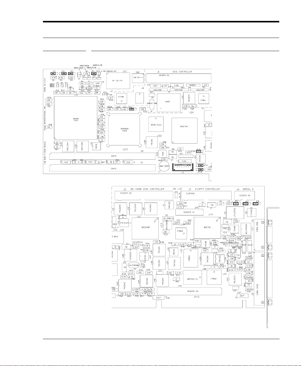
FIGURE 1
Right Half of
LS486
Left Half of
LS486
LS486/L486 CPU Card User’s Manual 11
Page 12

Getting Started
1.1 LS486 Components
The LS486 contains the components normally found on a plug-in
CPU card: a microprocessor, “headers” and “connectors,” a “dip
switch” block, “jumper” blocks, “SIMM” sockets, etc. Figure 1 provides the location of these components.
The microprocessor is the “brain” of the LS486, where basic arithmetic, logic and control functions are processed. The LS486 supports a 33-66 MHz 486DX/DX2 microprocessor.
Headers (also called “header/connector”) are components used to
connect peripherals (via connecting cables) to the LS486. For example, locate the “IDE Hard Drive” header on the LS486 (see Figure 1).
This header serves as a hard drive controller; you would use an
appropriate cable to connect an IDE hard drive to this header . Other
headers located on the LS486 include:
• a SCSI hard drive controller header (not included on the
L486 CPU Card)
• a floppy drive controller header
• a serial port header (also called “UART 2”) used to connect
serial devices (monitor, mouse, etc.) to the LS486
• two keyboard headers
Connectors are also used to connect external components to the
LS486, but, unlike headers, connectors are located on the I/O
bracket at the end of the LS486 board (which will make them accessible when you install the board, as we will discuss later). These
include a serial port connector (“UART 1”) and a parallel port
connector.
The LS486 dip switch block, known as SW1, is located at the top
of the board. It contains four (4) small dip switches, each of which
controls a different function. These switches are discussed in detail
in Section 1.2.1.
12 LS486/L486 CPU Card User’s Manual
Page 13

Before You Install the LS486
Jumper blocks (labeled “JP” in Figure 1) are small electronic components that contain pins, or small electronic leads, some of which
are connected via “jumpers.” These jumper blocks control certain
hardware options on the CPU Card. W e’ll also discuss jumper blocks
in Section 1.2.2.
SIMM (Single Inline Memory Module) sockets are located on the
left side of the LS486 Board. SIMM’s are “sticks” of DRAM
(Dynamic Random Access Memory) that can be inserted into these
sockets, providing extra memory. SIMM’s are discussed at length in
Chapter 6.
1.2 Before You Install the LS486
Now that you’re familiar with some key LS486 components, let’s
discuss those components you’ll need to check before you install
your LS486.
First, it is important to protect yourself and your equipment before
you perform any of the following procedures. Never touch the
LS486 while it is installed in the chassis and power is ON.
You should check the LS486 configuration before you install the
board. However, if the LS486 is already installed in your system,
remove power by turning all power switches OFF and disconnecting
all power cords from their power sources. Follow all safety precautions outlined by the chassis manufacturer. Only qualified, expe-
rienced electronics personnel should access the unit’s
interior. Also, do not touch the LS486 unless you are wearing
a static-dissipative device such as a grounding wrist strap.
Static electricity can damage sensitive LS486 components.
Before you install the LS486, check the dip switch and jumper set-
tings outlined in Sections 1.2.1 and 1.2.2. Pay particular attention
to the dip switch settings; the jumpers are preconfigured at the factory and are appropriate for most applications. Memory SIMM’s are
also installed at the factory.
LS486/L486 CPU Card User’s Manual 13
Page 14
Getting Started
1.2.1 Checking the Dip Switch Settings
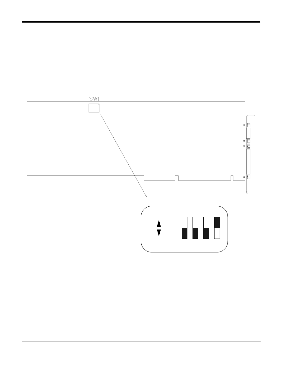
Locate Switch Block SW1, the four-switch block positioned at the
top of the LS486 board. Note that these switches are numbered,
from right to left, one (1) through four (4). Thus, the switch on the
far right side of the block is SW1, position 1, or SW1-1.
CLOSED
OPEN
1-4 1-3 1-2 1-1
SW1
SW1-1 is used to set the default monitor type. When SW1-1 is
CLOSED, the LS486 is configured to run with a color monitor.
When it is OPEN, SW1-1 is set to the monochrome monitor position. The LS486 is shipped with this switch CLOSED. If you’re
using a color monitor, be sure that SW1-1 is CLOSED. If you’re
using a monochrome monitor, OPEN this switch (of course, make
sure that no power is being fed to the LS486 before you touch the
switch).
14 LS486/L486 CPU Card User’s Manual
Page 15

Before You Install the LS486
SW1-2 controls the on-board ROM access. If you OPEN this switch,
the Flash memory is enabled and the auxiliary ROM is disabled. If
this switch is CLOSED, the auxiliary ROM is enabled, and the
Flash memory is disabled. The LS486 is shipped with this
switch OPEN.
SW1-3 is used in special cases when the CMOS RAM (Complemen-
tary Metallic Oxide Semiconductor Random Access Memory)
becomes corrupted. This condition is usually accompanied by a
“lock-up” of the system. The factory default values for LS486 operation must then be reloaded into CMOS RAM. Under normal conditions, SW1-3 should remain in the OPEN position. However,
when factory default values must be reloaded, see Section 5.3 for
proper procedures.
SW1-4 controls the configuration register I/O address. OPEN this
switch to set the I/O address to 270H. CLOSE this switch to set the
I/O address to 370H. The default for this switch is OPEN,
selecting I/O address 270H.
LS486/L486 CPU Card User’s Manual 15
Page 16
Getting Started
1.2.2 Checking the Jumper Block Settings
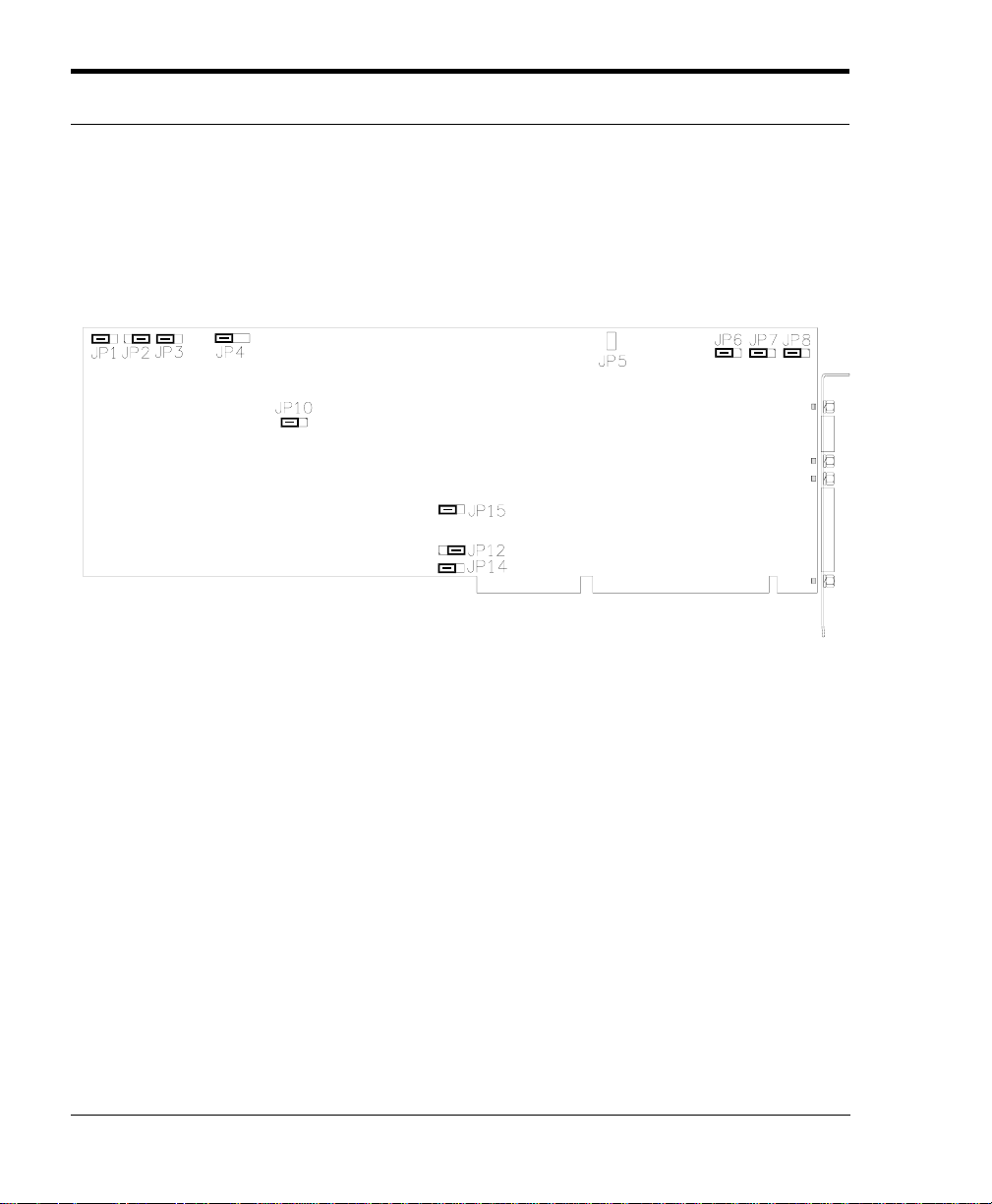
As discussed earlier, jumper blocks are small components containing electronic leads (called pins) sometimes connected by jumpers
(small conductors). These blocks have specific functions that are
affected by the presence and position of a jumper within the block.
Locations of these blocks are shown in the figure below.
Note: While you are facing the board, Pin 1 is on the far left for
Jumper Blocks JP1, JP2, JP3, JP4, JP12, JP14, and JP15. Pin 1 is
on the far right for JP6, JP7, JP8, and JP10. Pin 1 is the top pin for
JP5.
The following paragraphs provide more information about these
jumper blocks. If, after reading the descriptions , you w ant to change
the default jumper settings, do so with caution. Only experienced
electronics personnel should attempt to change these
jumper settings. Make sure that no power is being fed to the
LS486 and that you are wearing a grounding wrist strap or
other static-dissipative device. If you have questions, call Texas
Micro’s Technical Support Department (see page 3).
Jumper Block JP5 (located at the top of the board) is a two-pin
header that provides output for connecting a light-emitting diode
(LED) to indicate hard drive activity. Pin 1 (the top pin) of this block
is the anode (the positive electrode); Pin 2 is the cathode.
16 LS486/L486 CPU Card User’s Manual
Page 17
Before You Install the LS486
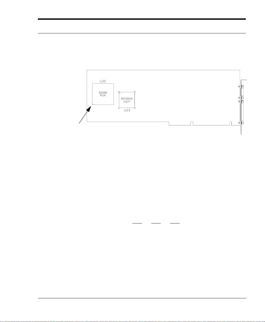
Jumper Block JP10, a three-pin strip, is used to select the processor type. The LS486 is equipped with an on-board 80486SX PQFP
processor, installed at location U23. However, an optional PGA processor can be installed in the U20 location illustrated below.
Pin 1
(“nicked corner”)
If you are using the on-board 80486SX PQFP processor , Pin 2
of JP10 should be jumpered to Pin 3. This is the factory
default. However, if you are using an optional PGA processor
installed in U20, Pin 1 should be jumpered to Pin 2.
Note: When installing a PGA processor, respect the orientation of Pin
1 (lower left corner) and use a heatsink. Ensure that all power has
been removed. Only qualified personnel should install this chip.
If you are using an optional PGA processor, Jumper Blocks
JP1, JP2 and JP3 are used to configure the LS486 to use the type
of PGA processor installed in U20.
JP1 JP2 JP3
486DX PGA 1-2 2-3 1-2
486SX PGA 2-3 1-2 2-3
487SX PGA 1-2 1-2 1-2
The factory default for these jumper blocks is the setting for
the 486DX PGA processor.
Note: User installation of a 486DX, 486DX2 or 487SX processor
could void the LS486/L486 warranty. Please contact Texas Micro’s
Technical Support department for information on upgrading.
LS486/L486 CPU Card User’s Manual 17
Page 18

Getting Started
Jumper Block JP4, a four-pin single-row block, allows you to
select the type of backup battery source employed by the LS486. By
jumpering Pin 1 to Pin 2, you select the LS486 on-board battery,
which is capable of saving CMOS RAM contents and maintaining
time of day for approximately 100,000 hours. If an external battery
is to be used, it should be plugged onto JP4 such that the “positive”
wire connects to Pin 1 and the “ground” wire connects to Pin 4. Note:
some external batteries come with a “plug” in Pin 2 (next to the “positive” wire) of the connector. This plug must be removed for use with a
TMI CPU board. The factory default is Pin 1 jumpered to Pin
2, on-board battery enabled. NOTE: Battery voltage should be
between 3.0 and 3.5 volts, with a 7.5 uA current drain at 3.5 volts.
Jumper Blocks JP6, JP7, and JP8 are three-pin blocks used to
select the configuration of UART2, the 10-pin header located at the
top right corner of the board. Jumpering Pins 2 and 3 of these three
blocks will configure UART2 for RS232 operation, while jumpering
Pins 1 and 2 of these blocks will select RS485/422 operation. The
default is Pins 2 to 3 jumpered, RS232 operation.
Jumper Blocks JP12 and JP14 control configuration and opera-
tion of the watchdog timer. The watchdog timer, when enabled, will
automatically reset the processor if no bus activity is detected for a
certain period of time. The watchdog timer is enabled by jumpering
Pins 1 and 2 of JP12. Jumpering Pins 2 and 3 of JP12 will disable
the watchdog timer. The factory default of JP12 is Pins 2 and 3
jumpered, watchdog timer disabled.
The watchdog timer reset time period is set by configuring JP14
according to the following:
JP14 - Pin 1 jumpered to Pin 2 1.2 seconds (default)
JP14 - Pin 2 jumpered to Pin 3 150ms
JP14 - No jumper 600ms
Jumper Block JP15 indicates the presence of the on-board SCSI
controller. Jumpering Pins 1-2 indicates that the SCSI controller is
present (LS486 board). Jumpering Pins 2-3 indicates that no SCSI
controller is on board (L486 board). This jumper block is preset at
the factory and should remain in the factory default position.
18 LS486/L486 CPU Card User’s Manual
Page 19

CHAPTER 2 LS486 Installation
Once you have checked all switches and jumper blocks to ensure
they match the desired configuration, you’re ready to install the
LS486 into an AT-compatible chassis backplane. However, before
installing the LS486 Card, consult the documentation provided with
the chassis. Installation instructions should be followed precisely.
CAUTION: Always remove power from the system before installing
the LS486. Follow all power-down procedures outlined in the chassis’
user’s manual. To ensure no injury occurs, disconnect the power cord
from the power source. Only qualified, experienced electronics personnel should access the interior of a chassis.
CAUTION: The components of the LS486 Card are very sensitive to
static discharge. Therefore, Texas Micro recommends using a
grounding wrist strap to remove all static electricity before touching
the components. While out of the unit, LS486 components should be
placed on a static-dissipative surface or into a static-shielding bag.
LS486/L486 CPU Card User’s Manual 19
Page 20

LS486 Installation
The procedure for installing the LS486 into a Texas Micro chassis is
described below.
1. Remove power from the chassis and disconnect all power cords.
Follow all power-down procedures outlined in your chassis’
user’s guide.
2. Remove the chassis cover, then detach the circuit card hold-
down bracket. This bracket stretches across the tops of the circuit cards and holds them in place.
3. Locate the desired bus location for installation (user’s choice,
although it is suggested that a location providing maximum distance between boards is chosen to allow proper ventilation).
4. Remove the I/O bracket spacer from the rear of the chassis. This
spacer occupies the area where the card’s I/O bracket is
accessed through the back of the chassis.
5. Attach the internal keyboard cable to the LS486. If you have
purchased the video daughter board, you should install it and
attach the video cable to it at this point.
6. Place the board ends into the appropriate card guide and card-
end slot in the chassis. Lower the LS486 into position and carefully push the card-edge connector into the slot. Ensure that the
I/O bracket is accessible through the back of the chassis.
7. Secure the card-edge I/O bracket to the hold-down lip.
8. Attach any required cables
9. After installing the LS486 and any other add-in cards desired,
secure all PC boards by appropriately positioning the card holddown bracket and securing it into place with the hardware provided for this purpose.
To install the LS486 into a passive backplane not manufactured by
Texas Micro, follow the instructions provided in this manual and
the installation information provided by the backplane
manufacturer.
Note: If installing a Texas Micro CPU in a non-TMI chassis, be sure
that the keyboard is correctly wired (connector J7). Refer to page 28
for the pinout of the keyboard connector.
20 LS486/L486 CPU Card User’s Manual
Page 21

CHAPTER 3 Connecting
P eripherals
The LS486 provides several headers/connectors for attaching
peripheral devices to the board:
• Two (2) serial ports
• One (1) parallel port
• Two keyboard interface header/connectors
• An IDE hard drive header/connector
• A SCSI hard drive header/connector (not available on the
L486 Card)
• A floppy drive header/connector
• An SVGA daughter board header/connector
This chapter supplies information and locations for each of these
components. Pinouts of each connector are also included. A pinout
identifies the function of each pin of a connector. Please note that,
while this information is valuable to electronics personnel, it is not
crucial to the everyday operation of the LS486. As long as the
proper cable is used and the connecting plug is properly inserted, a
supported peripheral should be operable when used with the LS486.
LS486/L486 CPU Card User’s Manual 21
Page 22

Connecting Peripherals
Please note the following cautions when connecting peripherals to
the LS486 CPU.
CAUTION: Always remove power from the system before connecting
peripherals to the LS486. To ensure no personal injury occurs, disconnect the power cord from the power source. Only qualified,
experienced electronics personnel should access the interior
of a chassis.
CAUTION: The components of the LS486 Card are very sensitive to
static discharge. Therefore, Texas Micro recommends using a
grounding wrist strap to remove all static electricity before touching
the components. While out of the unit, LS486 components should be
placed on a static-dissipative surface or into a static-shielding bag.
22 LS486/L486 CPU Card User’s Manual
Page 23

Serial Ports
3.1 Serial Ports
Let’s begin with the two serial ports. Serial ports allow you to connect serial devices (a serial mouse, serial printers, etc.) to the LS486
via appropriate serial cables. Serial ports are also known as UART
(Universal Asynchronous Receiver/Transmitter) ports.
Note that one serial port (UART 1), labeled J5 on the CPU card, is
located on the edge of the card (on the I/O bracket; see Figure 2).
This means that you can access UART 1 through the back of the
chassis after the LS486 is installed. UART 1 is an RS232-only
connector.
The other serial port (UART 2), labeled J4 in Figure 3, is located on
the card’s front surface. Accessing this port requires removal of the
chassis cover . Consult your chassis documentation for procedures on
removing the chassis cover, but remember to remove power
from the system and unplug the power cord before you
access the interior of the chassis. Most importantly, only
qualified, experienced electronics personnel should access
the interior of a chassis.
UART 2 can be configured as an RS232 or an RS422/485 serial
port via Jumper Blocks JP8, JP9 and JP10 (see Section 1.2.2). The
factory default is RS232. Be sure to use the proper cable when
connecting a serial device to the LS486 (9-pin DB9 interface connector - Part No. SCF1).
The graphic shown in Figure 2 describes the proper pin assignments when wiring a 25-pin connector to a 9-pin connector. If you
have any questions about this procedure, call Texas Micro’s Technical Support Department (see page 3).
More information about serial ports can be found in Section 5.2.2.
LS486/L486 CPU Card User’s Manual 23
Page 24
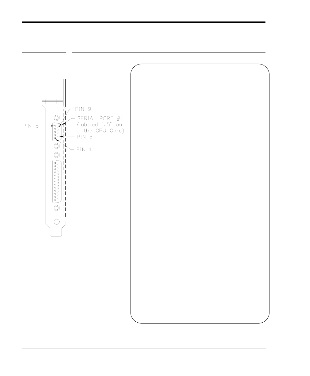
FIGURE 2
Connecting Peripherals
Pin Number Description (RS232)
1 DCD (Data Carrier Detect)
2 RXD (Receive Data)
3 TXD (Transmit Data)
4 DTR (Data Terminal Ready)
5 GND (Signal Ground)
6 DSR (Data Set Ready)
7 RTS (Request To Send)
8 CTS (Clear To Send)
9 RI (Ring Indicator)
To wire a 25-pin connector to a 9-pin connector,
use the following table:
DB9 DB25 Description
Pin Pin
1 8 DCD (Data Carrier Detect)
2 3 RXD (Receive Data)
3 2 TXD (Transmit Data)
4 20 DTR (Data Terminal Ready)
5 7 GND (Signal Ground)
6 6 DSR (Data Set Ready)
7 4 RTS (Request To Send)
8 5 CTS (Clear To Send)
9 22 RI (Ring Indicator)
24 LS486/L486 CPU Card User’s Manual
Page 25
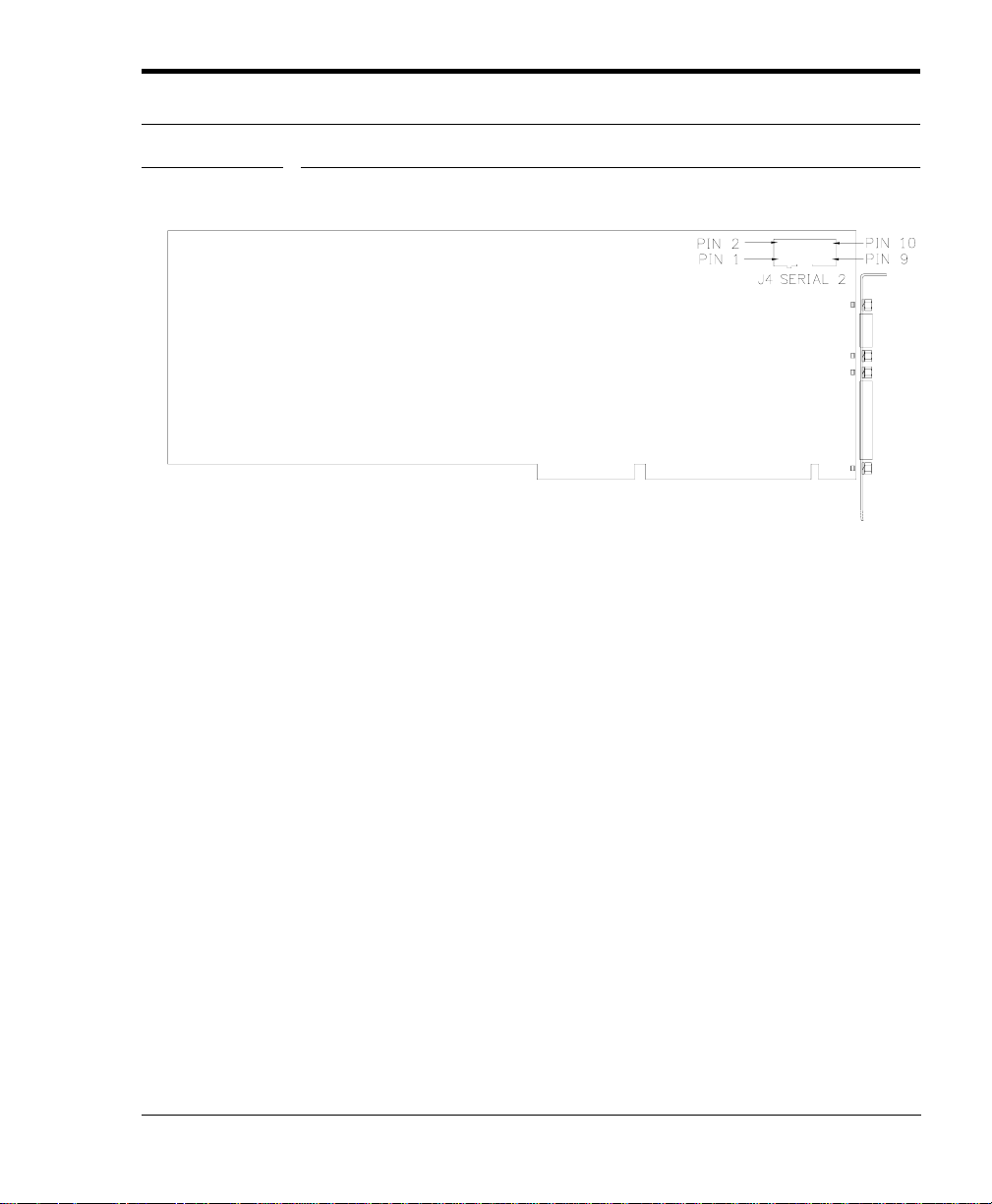
FIGURE 3
Serial Ports
RS232 RS422/485
Pin No. Description
1 DCD (Data Carrier Detect)
2 DSR (Data Set Ready)
3 RX (Receive Data)
4 RTS (Request To Send)
5 TX (Transmit Data)
6 CTS (Clear To Send)
7 DTR (Data Terminal Ready)
8 RI (Ring Indicator)
9 GND (Signal Ground)
10 VCC +5 (not used by
RS-232 signaling)
LS486/L486 CPU Card User’s Manual 25
Pin No. Description
1 Transmit 2 Transmit +
3 Receive +
4 Not Connected
5 Not Connected
6 Receive 7 Not Connected
8 Not Connected
9 GND (Signal Ground)
10 VCC +5 (not used by
RS-422 signaling)
Page 26
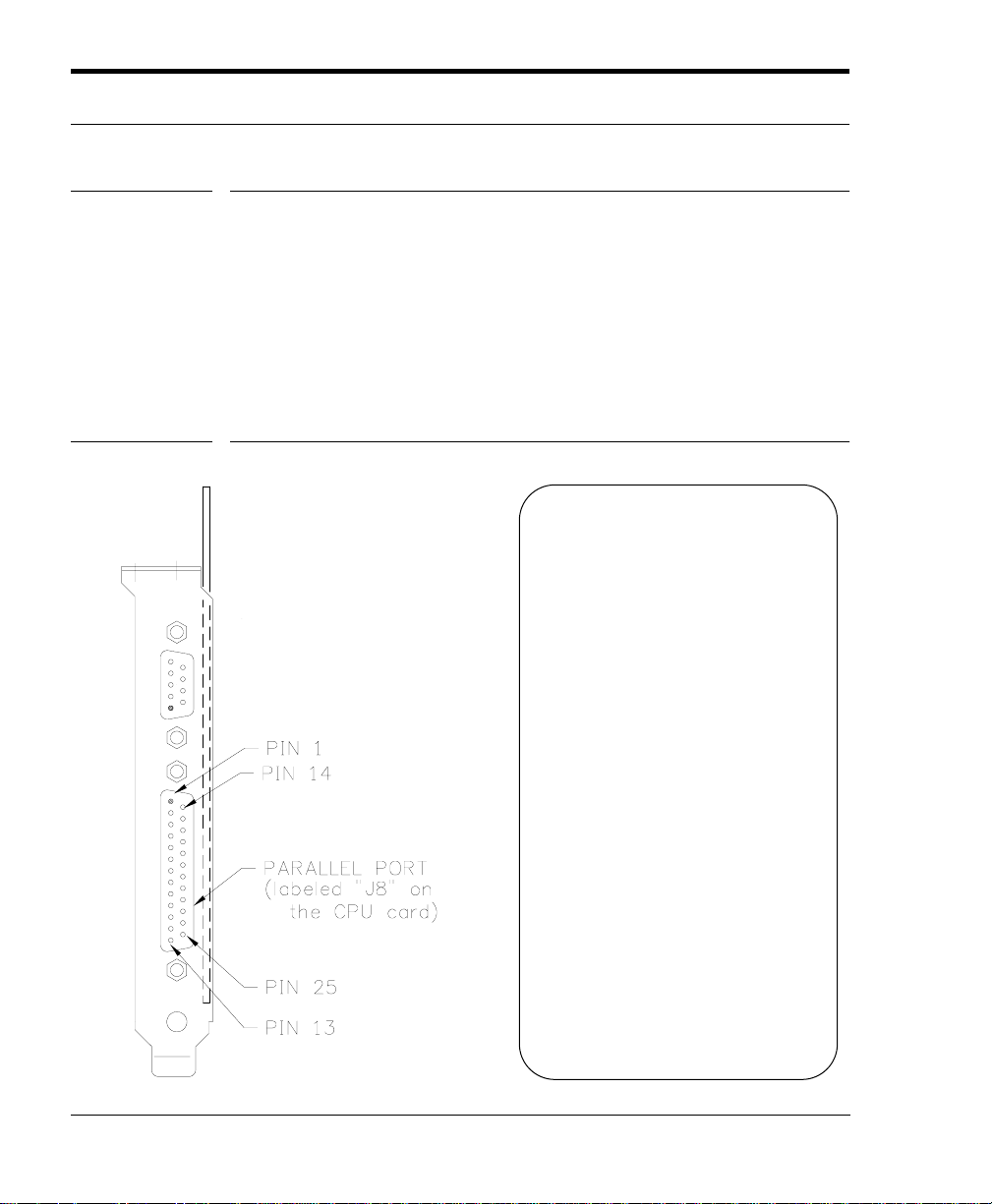
FIGURE 4
Connecting Peripherals
3.2 Parallel Port
The parallel port (Connector J8 on the CPU card) is normally used
for connecting a printer to the LS486. This port is a 25-pin connector located on the right edge of the LS486 (see Figure 4). Connect
the printer cable to this port for printer operation (of course, only
after removing system power and disconnecting the power cord).
More information on parallel ports and their configuration can be
found in Section 5.2.2.
Pin Number Description
1 -Strobe
2 + Data Bit 0
3 + Data Bit 1
4 + Data Bit 2
5 + Data Bit 3
6 + Data Bit 4
7 + Data Bit 5
8 + Data Bit 6
9 + Data Bit 7
10 - Acknowledge
11 + Busy
12 + Paper End
13 + Select
14 - Auto Feed
15 - Error
16 - Init. Printer
17 - Select Input
18-25 Ground
26 LS486/L486 CPU Card User’s Manual
Page 27

Keyboard Header/Connector
3.3 Keyboard Header/Connector
The LS486 also provides an 8-pin shrouded AT-compatible keyboard
header/connector at the bottom edge of the card. This pinout of this
header is shown in Figure 5.
Some connector manufacturers have reverse pin numbers. For the
LS486, Pin 1 is on the left (when viewing the chip side of the board
with the I/O bracket to the right).
The sockets on the Texas Micro keyboard connector cable are numbered in reverse order when compared to the pinout of the LS486
Keyboard Connector. For example, Socket 8 of the connector cable
corresponds with Pin 1 of the LS486 Keyboard Connector, Socket 7
of the cable corresponds with Pin 2 of the connector, etc.
Figure 5 provides proper connection procedures for the keyboard
interface cable. Ensure that the pins on the keyboard connector correspond with the pins on the cable connector.
LS486/L486 CPU Card User’s Manual 27
Page 28
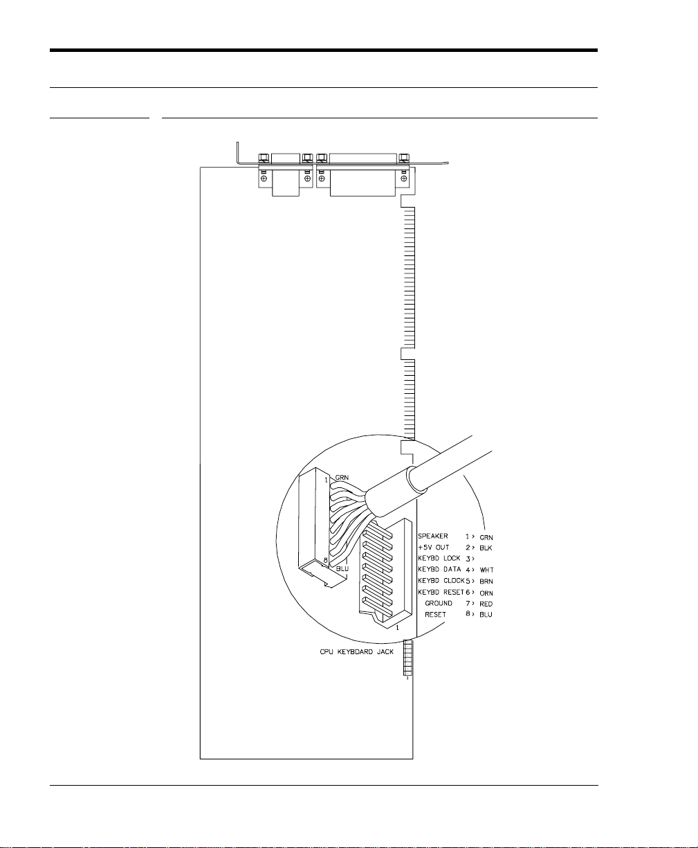
FIGURE 5
Connecting Peripherals
28 LS486/L486 CPU Card User’s Manual
Page 29
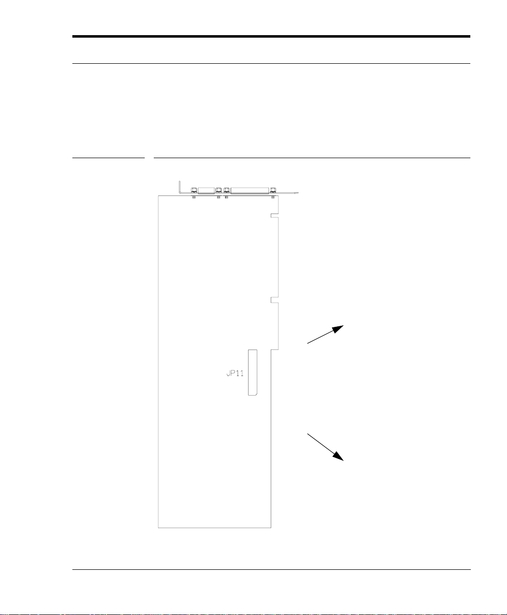
FIGURE 6
Keyboard Header/Connector
A second keyboard connector is available at Connector JP11. This is
a non-standard connector; do not attach a standard keyboard
to this connector . Also, do not connect keyboards to this connector and the standard keyboard connector (J7) at the
same time. The pinout of this optional connector is provided below.
+5V OUT
DATA
CLK
GND
LOCK (hardware KBD
lock signal)
RESET (the reset switch)
LS486/L486 CPU Card User’s Manual 29
Page 30
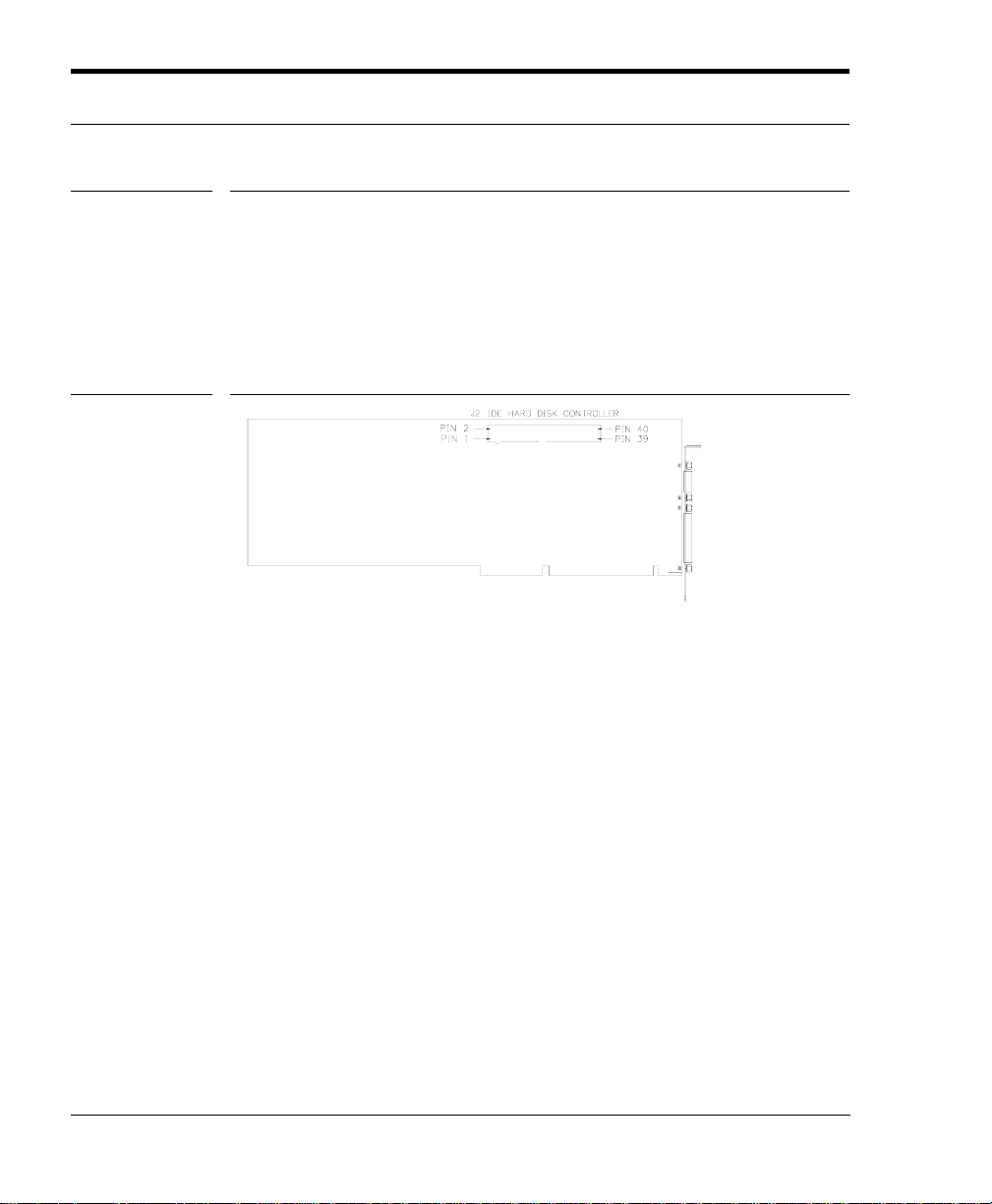
FIGURE 7
Connecting Peripherals
3.4 IDE Hard Drive Header/Connector
Two (2) Integrated Device Electronics (IDE) hard disk drives can be
attached to the LS486 board via J2 and a 40-conductor cable. The
pinout of J2, a 40-pin connector, is provided in Figure 7. Note: The
“red stripe” on the cable MUST be plugged in so that it is next to Pins
1 and 2. Otherwise, the hard drive will not work properly and/or the
hard drive may be damaged.
Pin Number Description
1 Reset, output
3 + Data 7, input/output
5 + Data 6, input/output
7 + Data 5, input/output
9 + Data 4, input/output
11 + Data 3, input/output
13 + Data 2, input/output
15 + Data 1, input/output
17 + Data 0, input/output
19 Ground
21 No connection
23 -I/O Write, output
25 -I/O Read, output
27 No connection
29 No connection
31 +IRQ14, input
33 +ADDR1, output
35 +ADDR0, output
37 -CS0, output
39 Activity Light, output
30 LS486/L486 CPU Card User’s Manual
Pin Number Description
2 Ground
4 + Data 8, input/output
6 + Data 9, input/output
8 + Data 10, input/output
10 + Data 11, input/output
12 + Data 12, input/output
14 + Data 13, input/output
16 + Data 14, input/output
18 + Data 15, input/output
20 No connection
22 Ground
24 Ground
26 Ground
28 +ALE, output
30 Ground
32 I/O CS16, output
34 No connection
36 +ADDR2, output
38 CS1, output
40 Ground
Page 31
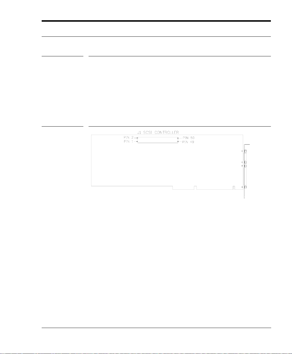
FIGURE 8
SCSI Hard Drive Header/Connector
3.5 SCSI Hard Drive Header/Connector
Note: This header is not present on the L486 CPU Card.
Two (2) Small Computer System Interface (SCSI) hard drives can
be attached to the LS486 via J1 and a 50-conductor cable. The
pinout of J1 is provided in Figure 8. See Section 5.1.3 for more information. Note: The “red stripe” on the cable must be plugged in so
that it is next to Pins 1 and 2. Otherwise, the CPU, cable and/or
SCSI drive may be damaged.
Pin Description
1 Ground
2 SCD0
3 Ground
4 SCD1
5 Ground
6 SCD2
7 Ground
8 SCD3
9 Ground
10 SCD4
11 Ground
12 SCD5
13 Ground
14 SCD6
15 Ground
16 SCD7
LS486/L486 CPU Card User’s Manual 31
Pin Description
18 SCDP
19 Ground
20 Ground
21 Ground
22 Ground
23 Ground
24 Ground
25 No connection
26 TERMPWR
27 Ground
28 Ground
29 Ground
30 Ground
31 Ground
32 ATN
33 Ground
34 Ground
Pin Description
35 Ground
36 BSY
37 Ground
38 ACK
39 Ground
40 RST
41 Ground
42 MSG
43 Ground
44 SEL
45 Ground
46 C/D
47 Ground
48 REQ
49 ATN
50 I/O
Page 32

Connecting Peripherals
Note: SCSI devices are daisy-chained with a cable, and both ends of
the cable are terminated. Terminators can be connected to either
SCSI devices or SCSI cables. Devices connected to these c hains must
contain the correct number of terminators for proper operation and
to prevent damage. No more than two terminators can exist in a
chain of SCSI devices - one at each end of the physical chain. If
more than two SCSI devices are connected in a SCSI daisy
chain, the middle device(s) in the control cable must have the
terminator resistor packs removed. On the LS486, these three (3)
resistor packs are located just below the SCSI connector. A fuse for
providing power to external terminating resistors is located at F1 on
the LS486.
3.6 Floppy Drive Header/Connector
Two floppy disk drives can be attached to the LS486 at J3 with a 34conductor flat cable no more than three (3) feet in length. Two connectors are spaced the desired distance at the drive end of the cable,
with Conductors 10 through 16 separated from the remainder of the
cable and twisted 180° between the two drive connectors.
The two installed drives may be any combination of 360 KByte and
1.2 MByte 5.25” drives or 720 KByte and 1.44 MByte 3.5” drives.
Both drives should be jumper-configured as Drive 1. DOS controls
the floppy disk drives; therefore, consult the DOS manual for
detailed information on disk operations. Consult Figure 9 for the J3
pinout.
Note: The “red stripe” on the floppy cable should be near Pins 1 and
2. Otherwise, the floppy drive will not work correctly and the CPU
and/or floppy drive may be damaged.
32 LS486/L486 CPU Card User’s Manual
Page 33
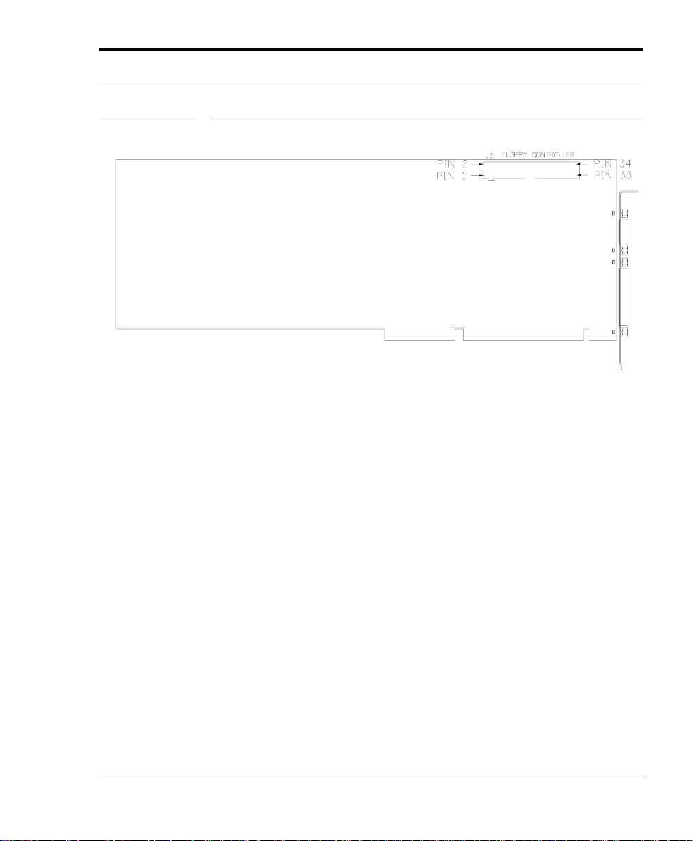
FIGURE 9
Floppy Drive Header/Connector
Pin Number Description
1 Ground
3 Ground
5 Ground
7 Ground
9 Ground
11 Ground
13 Ground
15 Ground
17 Ground
19 Ground
21 Ground
23 Ground
25 Ground
27 Ground
29 Ground
31 Ground
33 Ground
Pin Number Description
2 Disk speed change, output
4 No connection
6 No connection
8 Index detect, input, active low
10 Motor enable Drive A, output, active low
12 Select Drive B, output, active low
14 Select Drive A, output, active low
16 Motor enable Drive B, output, active low
18 Head step pulse, output, active low
20 Head step pulse, output, active low
22 Write data, output, active low
24 Write gate, output active low
26 Track 0 detect, input, active low
28 Write protect sense, input, active low
30 Read data, input, active high
32 Head select, output
34 Diskette change detect, input, active low
LS486/L486 CPU Card User’s Manual 33
Page 34
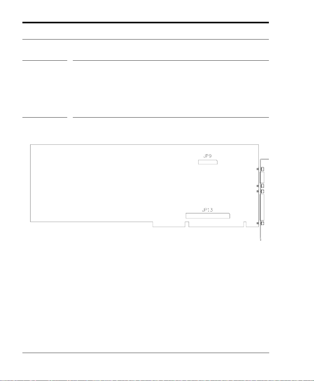
FIGURE 10
Connecting Peripherals
3.7 Video Daughter Board Connectors
The LS486 features two connectors (labeled JP9 and JP13) designated for L386VGA video daughter board connection. Locations of
these connectors are provided below in Figure 10. More information
about the L386VGA video daughter board can be found in the
“L386VGA User’s Manual” provided with the board.
34 LS486/L486 CPU Card User’s Manual
Page 35

CHAPTER 4 P ower-up
After all jumpers and switches have been checked, the LS486 has
been installed and all desired peripheral devices have been connected to the board, the LS486 is ready for power-up. However,
before you introduce power to the system, ensure that the operating
system you will be using is available on either Drive C or a diskette
in Drive A.
4.1 BIOS
When you power the system up, the LS486 BIOS (Basic Input Output System, a collection of driver and initialization software stored
on the CPU card, will perform checks and diagnostics, then search
for an operating system.
LS486/L486 CPU Card User’s Manual 35
Page 36

Power-up
4.2 Diagnostics
Upon power-up, the BIOS performs initialization routines, calculating memory size and configuration data to load into CMOS (Complimentary Metallic Oxide Semiconductor) memory. The BIOS then
performs internal diagnostics to compare the LS486’s current physical configuration with the configuration information recorded in
CMOS memory during setup. If inconsistencies exist, BIOS error
messages are displayed.
Some errors noted during power-up may be quickly corrected by verifying the setup information (see Chapter 5). Errors of greater complexity or a more technical nature may require the aid of trained
technical personnel. Contact Texas Micro’s Technical Support
Department (see page 3). Upon completion of the power-on diagnostics tests, the LS486 loads the operating system from disk or other
mass-storage device. However, if CMOS RAM contents are incorrect, the LS486 will prompt you to invoke the Setup Utility (see
Chapter 5).
4.3 Rebooting the LS486
If you wish to reboot the LS486, three (3) methods are acceptable:
1. Cycle power off and on.
2. Press <Ctrl-Alt-Del>.
3. Depress the system’s reset switch.
Using any of these methods to reboot the LS486 will result in system memory data loss. Therefore, it is suggested that, where possible, all processing be completed before reboot.
Next, you need to check all the configuration settings for the board
before you begin using it. Turn to Chapter 5 for information on the
LS486 Setup Utility.
36 LS486/L486 CPU Card User’s Manual
Page 37

QuickStart for
Advanced Users
This segment of the manual provides a “quickstart” feature for
advanced computer users. Included are procedures for:
• checking dip switch default settings
• checking jumper block default settings
• installing the LS486
• connecting peripherals to the LS486
• powering the system up
• accessing the Setup Utility
To configure the LS486 Board, perform the following:
1. Check dip switch settings.
Locate Switch Block SW1. The following are default settings.
• SW1-1 CLOSED - color monitor
• SW1-2 OPEN - flash ROM access
• SW1-3 OPEN - board uses setup configuration you provide
through the Setup Utility (see Chapter 5)
• SW1-4 OPEN - I/O config address 270h
If you want to change any of these settings, see Section 1.2.1.
LS486/L486 CPU Card User’s Manual 37
Page 38

Power-up
2.
Check jumper defaults.
Locate the LS486 jumper blocks. The defaults for these blocks
are as follows:
JP10 - Pin 2 jumpered to Pin 3 - using on-board 80486SX PQFP
processor.
JP1, JP2, and JP3 - set for 80486DX PGA chip use
(not applicable when on-board 486SX processor selected).
JP1 - Pin 1 jumpered to Pin 2
JP2 - Pin 2 jumpered to Pin 3
JP3 - Pin 1 jumpered to Pin 2
JP4 - Pin 1 jumpered to Pin 2 - on-board battery enabled.
JP6, JP7 and JP8 - Pin 2 jumpered to Pin 3 - UART 2 is RS232.
JP12 - Pin 2 jumpered to Pin 3 - watchdog timer disabled.
JP14 - Pin 1 jumpered to Pin 2 - 1.2 seconds for watchdog timer
reset (not applicable with watchdog timer disabled).
If you want to change any of these settings, see Section 1.2.2.
Note: JP15 should remain in the factory default configuration.
3. Install the LS486.
To install the LS486:
• Remove power from the system by turning all power
switches OFF and disconnecting the power cord from the
power source. Only qualified, experienced electronics personnel should access the interior of a chassis.
• Remove static electricity by wearing a static-dissipative
device (such as a grounding wrist strap). Place the board
on static-dissipative surfaces ONLY.
• Remove the I/O bracket spacer from the rear of the
chassis.
• Attach the keyboard cable to the CPU card. Note: If you
are using the L486VGA daughter board in conjunction
with the LS486, it should be installed now.
• Carefully lower and push the board into a card slot.
Ensure that the I/O bracket is accessible through the back
of the chassis.
• Secure the card-edge I/O bracket to the hold-down lip.
38 LS486/L486 CPU Card User’s Manual
Page 39

Rebooting the LS486
4.
Attach any required cables to the CPU card.
5. Connect peripherals to the LS486.
Before you connect any peripherals to the LS486, make sure
that no power is being applied to the LS486 Board and the
peripherals.
CAUTION: Always remove power from the system and peripherals before connecting the peripherals. To ensure no injury occurs,
disconnect all power cords from their power sources. Only qualified, experienced electronics personnel should access the interior
of a chassis.
CAUTION: The components of the LS486 Card are very sensitive to static discharge. Therefore, Texas Micro recommends
using a grounding wrist strap to remove all static electricity
before touching the components . While out of the unit, the components should be placed on a static-dissipative surface or into a
static-shielding bag.
Consult Chapter 3 for connector locations and pinouts.
6. Power the system up.
The BIOS will perform power-on checks, operate diagnostics
and invoke the internal setup routine. It will then direct the
media device to search for and load the operating system.
7. Access the Setup Utility.
The Setup Utility is a set of commands stored on the CPU card
and used to set the computer time, date and configuration data.
Configurable fields are stored in CMOS RAM. To access the
Setup Utility, press <Ctrl-Alt-S> during the memory test at
power-up.
.
LS486/L486 CPU Card User’s Manual 39
Page 40

Power-up
Scan Chapter 5, Using the Setup Utility, paying particular attention
to the “Basic Options” Menu, which is the first menu displayed
when the Setup Utility is accessed. Using <UP ARROW> and
<DOWN ARROW>, scroll through the Basic Options fields. If any
values need to be changed, press <ENTER> on that field, then use
the “hot” keys as described on the bottom line to make appropriate
changes.
Note: If you are using a monochrome VGA monitor, press F5 to turn
the color off to make the Setup Utility screen easier to read.
After you have configured the options in the Setup Utility, press
<ESC> (to save the changes and reboot) to reload your operating
system.
40 LS486/L486 CPU Card User’s Manual
Page 41

CHAPTER 5 Using the Setup
Utility
After all switches and jumpers have been checked, the LS486 has
been installed, peripherals have been connected and power has been
turned on, you are ready to access the LS486 Setup Utility.
The LS486 Setup Utility is a special set of commands that resides
on the CPU card and is used to set the computer time, date and configuration data. The Setup Utility can be accessed in two ways:
• By pressing <CTRL-ALT-DEL> during memory tests, or
• By pressing F2 when prompted by the BIOS during the
power-up operation. This occurs if the BIOS encounters
errors when trying to use the Setup Utility information (if
desired, you may press the F1 key to instruct the BIOS to
continue its diagnostics checks and attempt to load the
operating system).
LS486/L486 CPU Card User’s Manual 41
Page 42

Using the Setup Utility
The LS486 Setup Utility begins by displaying the screen pictured in
Figure 11. This screen is comprised of three (3) components:
• Options Menu
• Summary information
• Hot key descriptions
The Options Menu is located on the left side of the screen. This
menu contains a list of system parameters you can modify to meet
your system requirements. Use the UP/DOWN ARROW keys to
move the cursor up and down the list. When the cursor is on the
desired item, press the <ENTER> key to modify settings for that
specific topic.
The “summary information” area displays current system settings
and is located to the right of the Options Menu.
“Hot key” descriptions appear at the bottom of the screen. Press any
of these keys to perform its assigned function.
Note: If the BIOS detects the presence of an Adaptec 6360 SCSI controller, the name of the board in all menus and sign-on scripts will be
“LS486.” If no SCSI controller is present, the board will be referred
to as an “L486.”
42 LS486/L486 CPU Card User’s Manual
Page 43

FIGURE 11
Texas Microsystems, Inc. Setup Utility
Model LS486-SX 33MHz BIOS Version 4.0.1.3
Basic Options
Time ................................................10:18:28
Date................................................. Aug 30, 1993
Time and Date
Floppy Disks
Fixed Disks
Video Adapter
Keyboard
Shadow RAM
Boot Options
Password Options
Password Edit
Advanced Options
Park Hard Drive
Flash It!
Weekday..........................................Monday
Drive A............................................. 3
1
/2Inch, 1.44 MB
Drive B............................................. Not Installed
Hard Disk 1......................................SCSI Installed
Hard Disk 2......................................Not Installed
Video Adapter..................................VGA/EGA
Base Memory..................................640K
Extended Memory...........................3072K
Floating Point Unit........................... Not Present
Fast Boot......................................... No
Boot Drive Sequence ...................... Drive A: then C:
101-Keyboard NumLock..................Off‘
Password Protection........................ None
Boot Errors: Keyboard:...................On
Floppy:....................... On
Video:......................... On
↑ (prev) ↓ (next) F5 (color on/off) Esc (save/reboot)
LS486/L486 CPU Card User’s Manual 43
Page 44

Using the Setup Utility
5.1 Basic Options Menu
Locate the “Basic Options” menu. This list outlines all the parameters you can change through the Setup Utility. This menu is pictured below.
Basic Options
Time and Date
Floppy Disks
Fixed Disks
Video Adapter
Keyboard
Shadow RAM
Boot Options
Password Options
Password Edit
Advanced Options
Park Hard Drive
Flash It!
Note the “Advanced Options” item. Choosing this item will cause a
new menu of options to be displayed. We’ll discuss this menu in
Section 5.2. For now, let’s concentrate on each of the Basic Options
menu items. Remember, use the UP/DOWN ARROW keys to highlight an item, then the <ENTER> key to select that item.
44 LS486/L486 CPU Card User’s Manual
Page 45

FIGURE 12
Basic Options Menu
5.1.1 Time and Date
This option allows you to set the time and date in the batterybacked clock/calendar, which is used to set the DOS time and date
before the operating system is loaded.
Texas Microsystems, Inc. Setup Utility
Model LS486-SX 33MHz BIOS Version 4.0.1.3
Basic Options
Time and Date
Floppy Disks
Fixed Disks
Video Adapter
Keyboard
Shadow RAM
Boot Options
Password Options
Password Edit
Advanced Options
Park Hard Drive
Flash It!
↑(Previous) ↓ (Next) Spacebar (change) Enter (execute)
Time................................................ 10:18:28
Date................................................. Aug 30, 1993
Weekday......................................... Monday
Drive A ............................................ 3
Drive B ............................................ Not Installed
Hard Disk 1 ..................................... SCSI Installed
Hard Disk 2 ..................................... Not Installed
Video Adapter ................................. VGA/EGA
Base Memory.................................. 640K
Extended Memory........................... 3072K
Floating Point Unit........................... Not Present
Fast Boot......................................... No
Boot Drive Sequence...................... Drive A: then C:
101-Keyboard NumLock.................. Off
Password Protection ....................... None
Boot Errors: Keyboard:.................. On
Time: 09:43:02
Date: Aug 30, 1993
Weekday: Monday
Set Time and Date
Floppy:....................... On
Video: ........................ On
1
/2Inch, 1.44 MB
LS486/L486 CPU Card User’s Manual 45
Page 46
5.1.2 Floppy Disks
FIGURE 13 - A
Using the Setup Utility
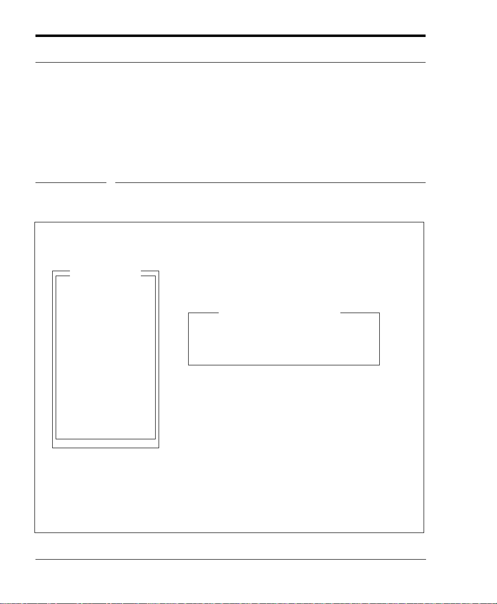
This feature allows you to configure the floppy drive subsystem. The
first menu asks if you want to enable the LS486 on-board controller.
In addition, the Setup Utility will request the drive types for floppy
drives A: and B:. Finally, you will be asked if you want to enable or
disable floppy drive configuration errors. If disabled, this option
allows you to run the system without a floppy disk drive.
Texas Microsystems, Inc. Setup Utility
Model LS486-SX 33MHz BIOS Version 4.0.1.3
Basic Options
Time and Date
Floppy Disks
Fixed Disks
Video Adapter
Keyboard
Shadow RAM
Boot Options
Password Options
Password Edit
Advanced Options
Park Hard Drive
Flash It!
↑(Previous) ↓ (Next) Enter (execute) Esc (quit/save)
Time................................................ 10:18:28
Date................................................. Aug 30, 1993
Weekday......................................... Monday
Drive A ............................................ 3
Drive B ............................................ Not Installed
Hard Disk 1 ..................................... SCSI Installed
Hard Disk 2 ..................................... Not Installed
Video Adapter ................................. VGA/EGA
Base Memory.................................. 640K
Extended Memory........................... 3072K
Floating Point Unit........................... Not Present
Fast Boot......................................... No
Boot Drive Sequence...................... Drive A: then C:
101-Keyboard NumLock.................. Off
Password Protection ....................... None
Boot Errors: Keyboard:.................. On
Onboard Floppy Controller
Off
On
Floppy:....................... On
Video: ........................ On
1
/2Inch, 1.44 MB
46 LS486/L486 CPU Card User’s Manual
Page 47
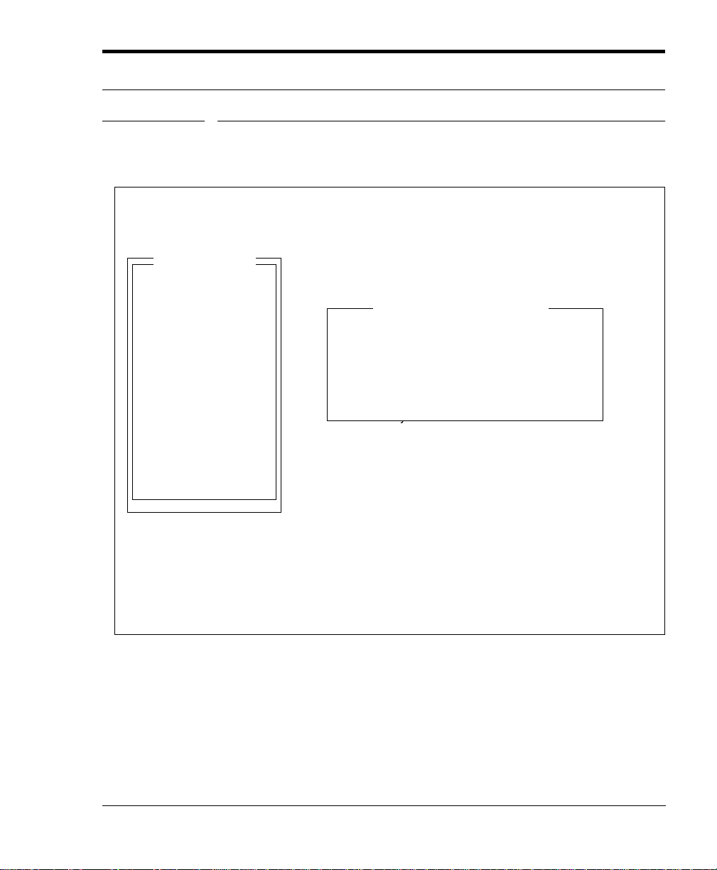
FIGURE 13 - B
Basic Options Menu
Texas Microsystems, Inc. Setup Utility
Model LS486-SX 33MHz BIOS Version 4.0.1.3
Basic Options
Time.................................................10:18:28
Date.................................................Aug 30, 1993
Time and Date
Floppy Disks
Fixed Disks
Video Adapter
Keyboard
Shadow RAM
Boot Options
Password Options
Password Edit
Advanced Options
Weekday..........................................Monday
Select Drive A: Type
Drive A.............................................3
Drive B.............................................Not Installed
Hard Disk 1......................................SCSI Installed
Hard Disk 2......................................Not Installed
Video Adapter..................................VGA/EGA
Not Installed
1
5
/
Inch, 360 KB
4
1
5
/
Inch, 1.2 MB
4
1
3
/
Inch, 720 KB
2
1
3
/
Inch, 1.44 MB
2
1
/2Inch, 1.44 MB
Base Memory...................................640K
Extended Memory............................3072K
Floating Point Unit............................Not Present
Park Hard Drive
Flash It!
Fast Boot..........................................No
Boot Drive Sequence.......................Drive A: then C:
101-Keyboard NumLock ..................Off
Password Protection........................None
Boot Errors: Keyboard:...................On
Floppy:........................On
Video:.........................On
↑(Previous) ↓ (Next) Enter (execute) Esc (quit/save)
LS486/L486 CPU Card User’s Manual 47
Page 48
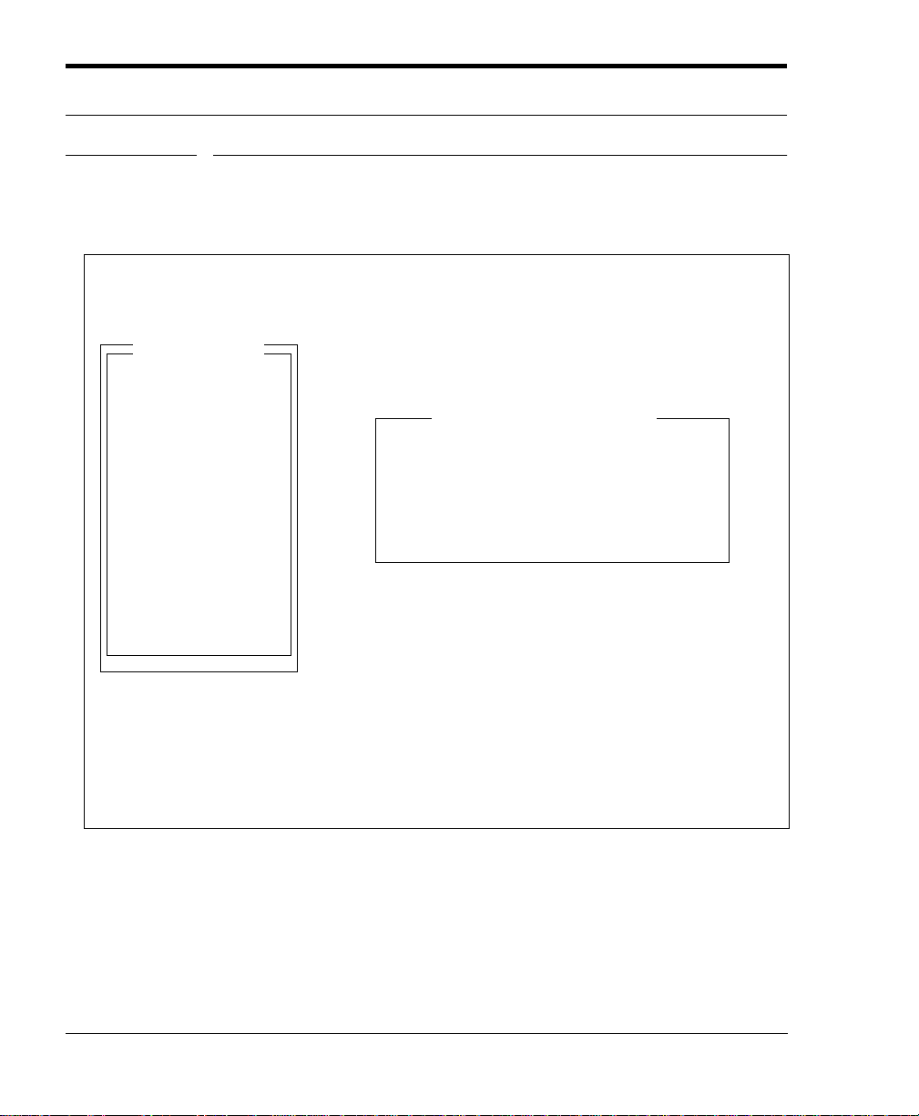
FIGURE 13 - C
Using the Setup Utility
Texas Microsystems, Inc. Setup Utility
Model LS486-SX 33MHz BIOS Version 4.0.1.3
Basic Options
Time.................................................10:18:28
Date.................................................Aug 30, 1993
Time and Date
Floppy Disks
Fixed Disks
Video Adapter
Keyboard
Shadow RAM
Boot Options
Password Options
Password Edit
Advanced Options
Weekday..........................................Monday
Drive A.............................................3
Drive B.............................................Not Installed
Hard Disk 1......................................SCSI Installed
Hard Disk 2......................................Not Installed
Video Adapter..................................VGA/EGA
Base Memory ..................................640K
Select Drive B: Type
Not Installed
1
5
/
Inch, 360 KB
4
1
5
/
Inch, 1.2 MB
4
1
3
/
Inch, 720 KB
2
1
3
/
Inch, 1.44 MB
2
1
/2Inch, 1.44 MB
Extended Memory ...........................3072K
Floating Point Unit ...........................Not Present
Park Hard Drive
Flash It!
Fast Boot .........................................No
Boot Drive Sequence.......................Drive A: then C:
101-Keyboard NumLock..................Off
Password Protection........................None
Boot Errors: Keyboard:...................On
Floppy: .......................On
Video:.........................On
↑(Previous) ↓ (Next) Enter (execute) Esc (quit/save)
48 LS486/L486 CPU Card User’s Manual
Page 49
FIGURE 13 - D
Basic Options Menu
Texas Microsystems, Inc. Setup Utility
Model LS486-SX 33MHz BIOS Version 4.0.1.3
Basic Options
Time................................................ 10:18:28
Date................................................. Aug 30, 1993
Time and Date
Floppy Disks
Fixed Disks
Video Adapter
Keyboard
Shadow RAM
Boot Options
Weekday......................................... Monday
Floppy Configuration Errors
Drive A ............................................ 3
Drive B ............................................ Not Installed
Hard Disk 1 ..................................... SCSI Installed
Off
On
1
/2Inch, 1.44 MB
Hard Disk 2 ..................................... Not Installed
Video Adapter .................................VGA/EGA
Password Options
Password Edit
Advanced Options
Base Memory.................................. 640K
Extended Memory........................... 3072K
Floating Point Unit........................... Not Present
Park Hard Drive
Flash It!
Fast Boot......................................... No
Boot Drive Sequence...................... Drive A: then C:
101-Keyboard NumLock.................. Off
Password Protection ....................... None
Boot Errors: Keyboard:.................. On
Floppy:....................... On
Video: ........................ On
↑(Previous) ↓ (Next) Enter (execute) Esc (quit/save)
LS486/L486 CPU Card User’s Manual 49
Page 50

Using the Setup Utility
5.1.3 Fixed Disks
This option allows the user to configure the fixed (hard) disk subsystem, including the on-board SCSI controller. When you select
this field, you will be asked whether you want to turn the LS486 onboard IDE controller on or off. In addition, the Setup Utility will
request the drive type for hard disk 1 (C:) and hard disk 2 (D:)
An “Auto ID” feature is invoked if you press F2 while the “Hard
Disk 1” menu is displayed. This option will analyze your hard drive
and provide a drive type ID, gleaned from the standard hard drive
parameter table (HDPT), that most closely matches the characteristics of your hard drive. Note: This option is also available for the
“Hard Disk 2” menu. To accept this drive type ID, press ENTER.
Pressing the PgUp key will invoke a search through the HDPT for
the next closest match.
If you continue to press the PgUp key, the menu will eventually display the user-configurable types “46” and “47.” Types 46 and/or 47
will also be offered if no HDPT match is found when the “Auto ID”
feature is invoked. These types allow you to set the hard disk configuration fields to match the characteristics of your hard disks.
If you want to change any of the fields offered by type 46 or 47, press
ENTER to accept the values shown. Invoke the “Fixed Disks” option
from the “Basic Options” menu, then re-enter the “Set Hard Drive”
menu. You may now set the fields to the desired values.
Note: The remainder of this section pertains to LS486 users only. The
L486 board does not contain an on-board SCSI controller.
The on-board SCSI controller is the Adaptec 6360 single-chip I/O
processor . W ith a 128-byte data FIFO , the 6360 can burst data at up
to 10 MBytes/second across the host bus. On the SCSI bus, it can
support synchronous data transfers at up to 10 MBytes/second.
The LS486 on-board SCSI BIOS can be disabled or enabled at
E0000. If enabled, the SCSI BIOS will enable the on-board 6360
SCSI controller chip. The on-board SCSI can also be used by booting
from another disk and loading a driver for the 6360 controller.
50 LS486/L486 CPU Card User’s Manual
Page 51
FIGURE 14 - A
Basic Options Menu
The IRQ for the on-board SCSI controller can be selected as IRQ9,
IRQ10, IRQ11, IRQ12, or NONE. If the on-board SCSI controller is
not being used, be sure to select NONE.
The base I/O port address for the on-board SCSI controller can be
selected as either 140 or 340. If the SCSI controller is used for the
bootable drive, select 340 as the SCSI controller I/O base address,
and use the on-board ROM at E000. If the on-board SCSI controller
is not using the on-board ROM, but instead is using a driver or
another ROM, the SCSI controller I/O base address can be 340 or
140. Be sure this address does not conflict with other port addresses
(especially other SCSI controllers).
Texas Microsystems, Inc. Setup Utility
Model LS486-SX 33MHz BIOS Version 4.0.1.3
Basic Options
Time and Date
Floppy Disks
Fixed Disks
Video Adapter
Keyboard
Shadow RAM
Boot Options
Password Options
Password Edit
Advanced Options
Park Hard Drive
Flash It!
↑(Previous) ↓ (Next) Enter (execute) Esc (quit/save)
Time................................................ 10:18:28
Date................................................. Aug 30, 1993
Weekday......................................... Monday
Drive A ............................................ 3
Drive B ............................................ Not Installed
Hard Disk 1 ..................................... SCSI Installed
Hard Disk 2 ..................................... Not Installed
Video Adapter .................................VGA/EGA
Base Memory.................................. 640K
Extended Memory........................... 3072K
Floating Point Unit........................... Not Present
Fast Boot......................................... No
Boot Drive Sequence...................... Drive A: then C:
101-Keyboard NumLock.................. Off
Password Protection ....................... None
Boot Errors: Keyboard:.................. On
LS486/L486 CPU Card User’s Manual 51
Onboard IDE Interface
Off
On
Floppy:....................... On
Video: ........................ On
1
/2Inch, 1.44 MB
Page 52
FIGURE 14 - B
Using the Setup Utility
Texas Microsystems, Inc. Setup Utility
Model LS486-SX 33MHz BIOS Version 4.0.1.3
Basic Options
Time ................................................ 10:18:28
Date................................................. Aug 30, 1993
Time and Date
Floppy Disks
Fixed Disks
Video Adapter
Keyboard
Shadow RAM
Boot Options
Password Options
Password Edit
Advanced Options
Park Hard Drive
Flash It!
Weekday..........................................Monday
Drive A............................................. 3
Drive B............................................. Not Installed
Hard Disk 1......................................SCSI Installed
Hard Disk 2......................................Not Installed
Video Adapter..................................VGA/EGA
Type ..............................44
Cylinders..................... 820
Heads.............................. 6
Landing Zone.............. 820
Set Hard Disk 1 Type
1
/2Inch, 1.44 MB
Write Precomp...............-1
Base Memory..................................640K
Extended Memory...........................3072K
Sectors.......................... 17
Size............................... 40
Floating Point Unit........................... Not Present
Fast Boot......................................... No
Boot Drive Sequence ...................... Drive A: then C:
101-Keyboard NumLock..................Off
Password Protection........................ None
Boot Errors: Keyboard:...................On
Floppy:....................... On
Video:......................... On
Pg Up (next) Pg Down (previous) F2 (Auto ID) Enter (execute)
52 LS486/L486 CPU Card User’s Manual
Page 53
FIGURE 14 - C
Basic Options Menu
Texas Microsystems, Inc. Setup Utility
Model LS486-SX 33MHz BIOS Version 4.0.1.3
Basic Options
Time................................................ 10:18:28
Date ................................................ Aug 30, 1993
Time and Date
Floppy Disks
Fixed Disks
Video Adapter
Keyboard
Shadow RAM
Boot Options
Password Options
Password Edit
Advanced Options
Park Hard Drive
Flash It!
Weekday......................................... Monday
Auto ID
Drive A ............................................ 3
Drive B ............................................ Not Installed
Hard Disk 1 ..................................... SCSI Installed
Hard Disk 2 ..................................... Not Installed
Video Adapter ................................. VGA/EGA
Drive Reports:
Cylinders.................1024
Heads ...........................2
Sectors........................40
Drive Table Match:
1
/2Inch, 1.44 MB
Type ............................17
Base Memory.................................. 640K
Extended Memory........................... 3072K
Floating Point Unit........................... Not Present
Fast Boot......................................... No
Boot Drive Sequence...................... Drive A: then C:
101-Keyboard NumLock.................. Off‘
Cylinders...................977
Heads ...........................5
Landing Zone:...........977
Write Precomp..........300
Sectors........................17
Size.............................40
Password Protection ....................... None
Boot Errors: Keyboard:.................. On
Floppy:....................... On
Video: ........................ On
ENTER (Accept) Pg Up (Next match) ESC (Exit)
LS486/L486 CPU Card User’s Manual 53
Page 54
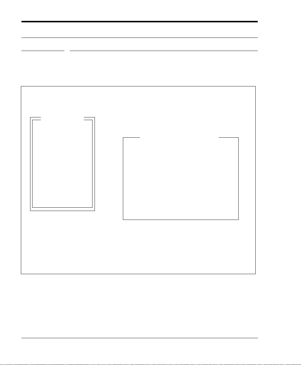
FIGURE 14 - D
Using the Setup Utility
Texas Microsystems, Inc. Setup Utility
Model LS486-SX 33MHz BIOS Version 4.0.1.3
Basic Options
Time and Date
Floppy Disks
Fixed Disks
Video Adapter
Keyboard
Shadow RAM
Boot Options
Password Options
Password Edit
Advanced Options
Park Hard Drive
ENTER (Accept) ESC (Exit)
Time................................................ 10:18:28
Date ................................................ Aug 30, 1993
Weekday......................................... Monday
Auto ID
Drive A ............................................ 3
Drive B ............................................ Not Installed
Hard Disk 1 ..................................... SCSI Installed
Hard Disk 2 ..................................... Not Installed
Video Adapter ................................. VGA/EGA
Drive Reports:
Cylinders.................1053
Heads ...........................2
Sectors........................40
Optional user configurable:
1
/2Inch, 1.44 MB
Type ............................47
Base Memory.................................. 640K
Extended Memory........................... 3072K
Floating Point Unit........................... Not Present
Fast Boot......................................... No
Boot Drive Sequence...................... Drive A: then C:
101-Keyboard NumLock.................. Off‘
Cylinders.................1053
Heads ...........................2
Landing Zone:.........1053
Write Precomp............ -1
Sectors........................40
Size.............................41
Password Protection ....................... None
Boot Errors: Keyboard:.................. On
Floppy:....................... On
Video: ........................ On
54 LS486/L486 CPU Card User’s Manual
Page 55
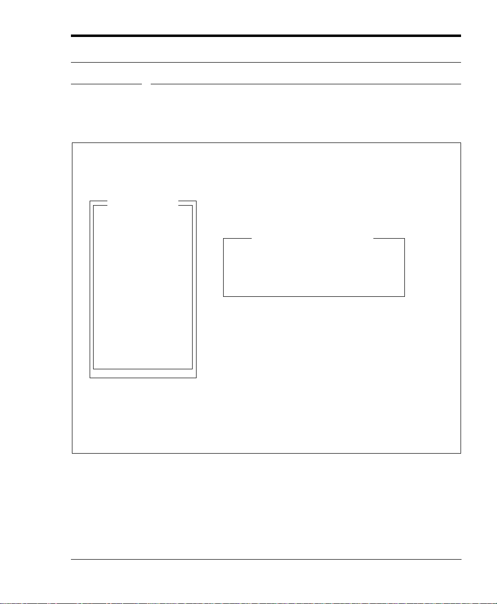
FIGURE 14 - E
Basic Options Menu
Texas Microsystems, Inc. Setup Utility
Model LS486-SX 33MHz BIOS Version 4.0.1.3
Basic Options
Time.................................................10:18:28
Date .................................................Aug 30, 1993
Time and Date
Floppy Disks
Fixed Disks
Video Adapter
Keyboard
Shadow RAM
Boot Options
Weekday..........................................Monday
Drive A.............................................3
Onboard SCSI ROM
1
/2Inch, 1.44 MB
Drive B.............................................Not Installed
Hard Disk 1......................................SCSI Installed
Hard Disk 2......................................Not Installed
Off
E0000H
Video Adapter..................................VGA/EGA
Password Options
Password Edit
Advanced Options
Base Memory...................................640K
Extended Memory............................3072K
Floating Point Unit............................Not Present
Park Hard Drive
Flash It!
Fast Boot..........................................No
Boot Drive Sequence.......................Drive A: then C:
101-Keyboard NumLock ..................Off
Password Protection........................None
Boot Errors: Keyboard:...................On
Floppy:........................On
Video:.........................On
↑(Previous) ↓ (Next) Enter (execute) Esc (quit/save)
LS486/L486 CPU Card User’s Manual 55
Page 56
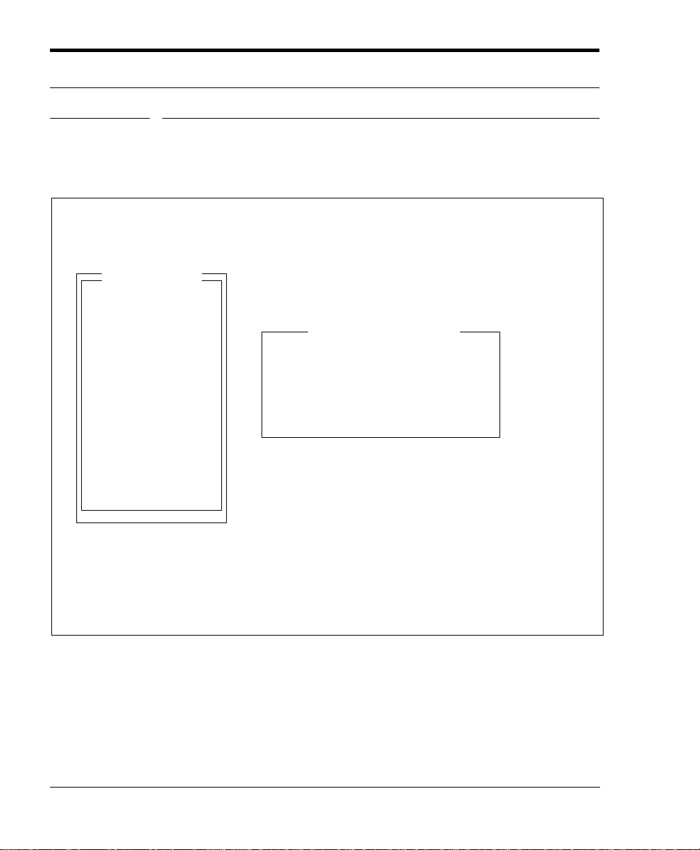
FIGURE 14 - F
Using the Setup Utility
Texas Microsystems, Inc. Setup Utility
Model LS486-SX 33MHz BIOS Version 4.0.1.3
Basic Options
Time and Date
Floppy Disks
Fixed Disks
Video Adapter
Keyboard
Shadow RAM
Boot Options
Password Options
Password Edit
Advanced Options
Park Hard Drive
Flash It!
↑(Previous) ↓ (Next) Enter (execute) Esc (quit/save)
Time.................................................10:18:28
Date .................................................Aug 30, 1993
Weekday..........................................Monday
Drive A.............................................3
Drive B.............................................Not Installed
Hard Disk 1......................................SCSI Installed
Hard Disk 2......................................Not Installed
Video Adapter..................................VGA/EGA
Base Memory...................................640K
Extended Memory............................3072K
Floating Point Unit............................Not Present
Fast Boot..........................................No
Boot Drive Sequence.......................Drive A: then C:
101-Keyboard NumLock ..................Off
Password Protection........................None
Boot Errors: Keyboard:...................On
Select SCSI IRQ
IRQ9
IRQ10
IRQ11
IRQ12
NONE
Floppy:........................On
Video:.........................On
1
/2Inch, 1.44 MB
56 LS486/L486 CPU Card User’s Manual
Page 57
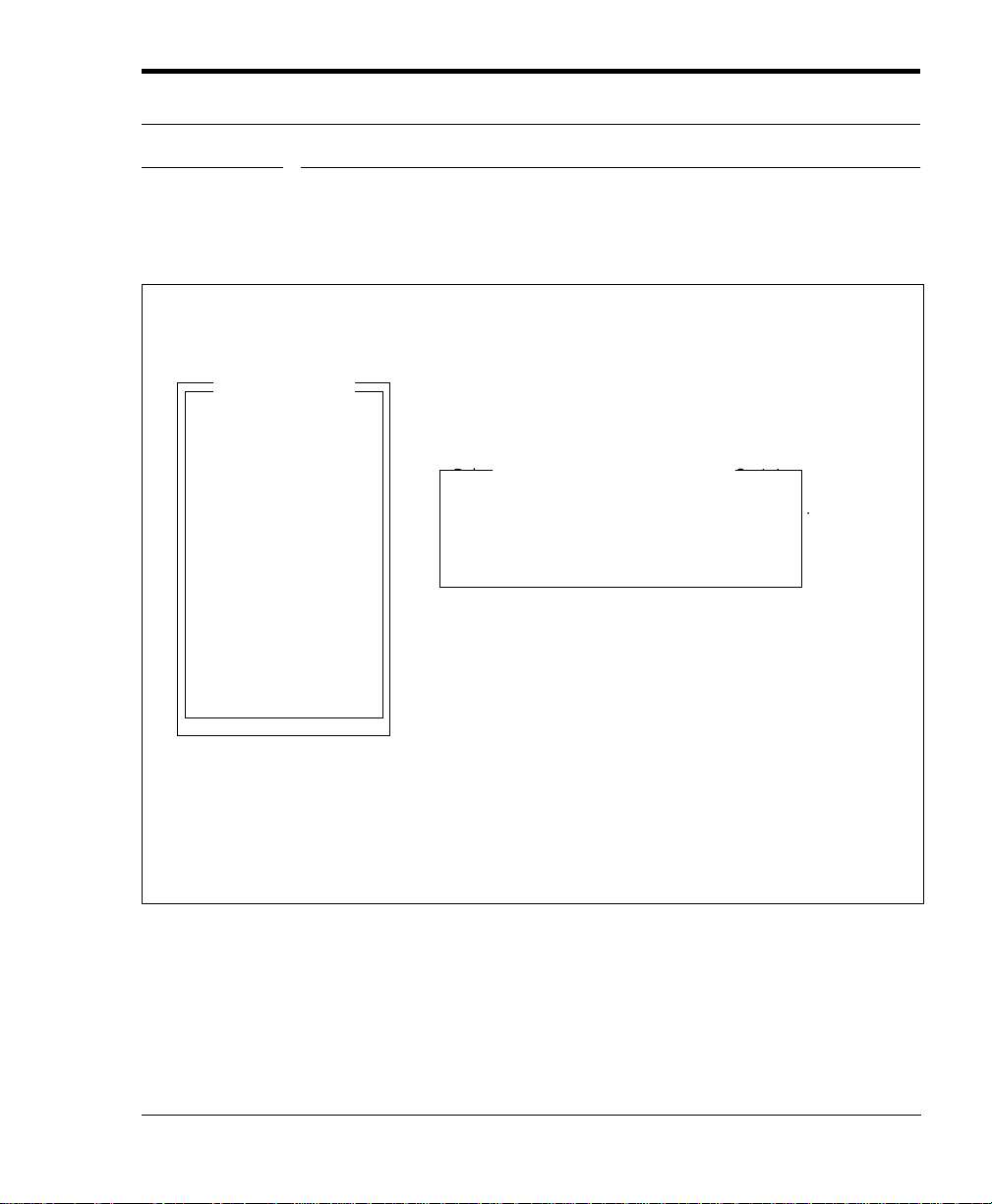
FIGURE 14 - G
Basic Options Menu
Texas Microsystems, Inc. Setup Utility
Model LS486-SX 33MHz BIOS Version 4.0.1.3
Basic Options
Time ................................................ 10:18:28
Date................................................. Aug 30, 1993
Time and Date
Floppy Disks
Fixed Disks
Video Adapter
Keyboard
Shadow RAM
Boot Options
Weekday..........................................Monday
Drive A............................................. 3
Select SCSI I/O PORT
1
/2Inch, 1.44 MB
Drive B............................................. Not Installed
Hard Disk 1......................................SCSI Installed
Hard Disk 2......................................Not Installed
Select SCSI IRQ
140H
340H
Video Adapter..................................VGA/EGA
Password Options
Password Edit
Advanced Options
Base Memory..................................640K
Extended Memory...........................3072K
Floating Point Unit........................... Not Present
Park Hard Drive
Flash It!
Fast Boot......................................... No
Boot Drive Sequence ...................... Drive A: then C:
101-Keyboard NumLock..................Off
Password Protection........................ None
Boot Errors: Keyboard:...................On
Floppy:....................... On
Video:......................... On
↑(Previous) ↓ (Next) Enter (execute) Esc (quit/save)
LS486/L486 CPU Card User’s Manual 57
Page 58
5.1.4 Video Adapter
FIGURE 15 - A
Using the Setup Utility
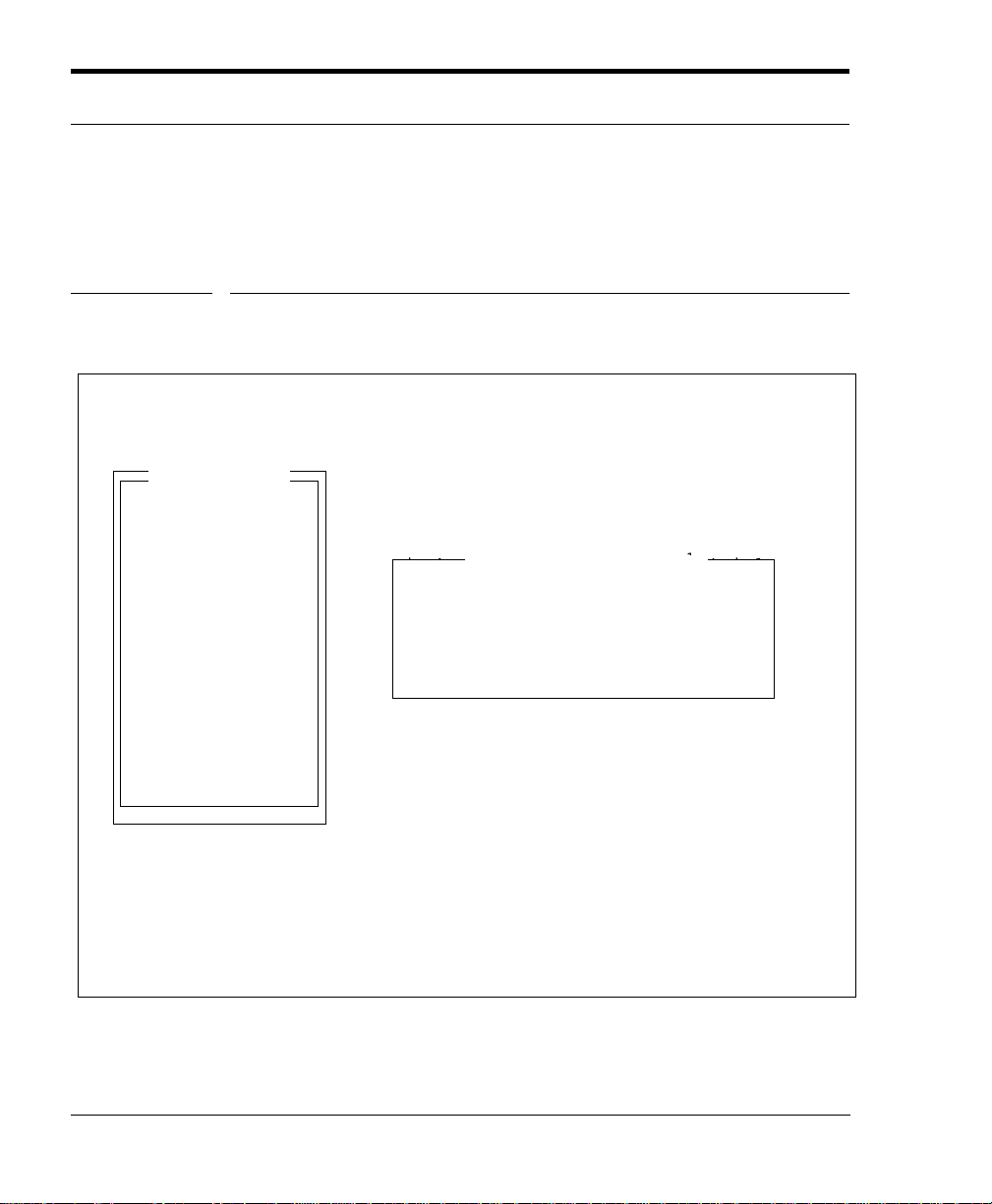
This feature allows you to specify the type of video adapter installed
in your system. In addition, video configuration errors can be disabled, allowing you to run your system without a video adapter.
Texas Microsystems, Inc. Setup Utility
Model LS486-SX 33MHz BIOS Version 4.0.1.3
Basic Options
Time and Date
Floppy Disks
Fixed Disks
Video Adapter
Keyboard
Shadow RAM
Boot Options
Password Options
Password Edit
Advanced Options
Park Hard Drive
Flash It!
↑(Previous) ↓ (Next) Enter (execute) Esc (quit/save)
Time ................................................ 10:18:28
Date................................................. Aug 30, 1993
Weekday..........................................Monday
Drive A............................................. 3
Drive B............................................. Not Installed
Hard Disk 1......................................SCSI Installed
Hard Disk 2......................................Not Installed
Video Adapter..................................VGA/EGA
Base Memory..................................640K
Extended Memory...........................3072K
Floating Point Unit........................... Not Present
Fast Boot......................................... No
Boot Drive Sequence ...................... Drive A: then C:
101-Keyboard NumLock..................Off
Password Protection........................ None
Boot Errors: Keyboard:...................On
Select Video Adapter Type
VGA/EGA
CGA 40 x 25
CGA 80 x 25
Monochrome
Floppy:....................... On
Video:......................... On
1
/2Inch, 1.44 MB
58 LS486/L486 CPU Card User’s Manual
Page 59
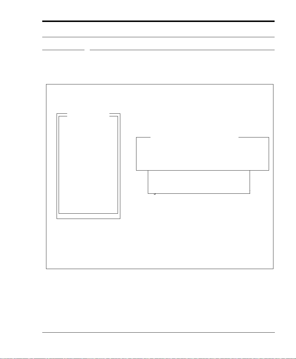
FIGURE 15 - B
Basic Options Menu
Texas Microsystems, Inc. Setup Utility
Model LS486-SX 33MHz BIOS Version 4.0.1.3
Basic Options
Time................................................ 10:18:28
Date................................................. Aug 30, 1993
Time and Date
Floppy Disks
Fixed Disks
Video Adapter
Keyboard
Shadow RAM
Boot Options
Password Options
Password Edit
Advanced Options
Weekday......................................... Monday
Drive A ............................................ 3
Drive B ............................................ Not Installed
Hard Disk 1 ..................................... SCSI Installed
Hard Disk 2 ..................................... Not Installed
Video Adapter ................................. VGA/EGA
Base Memory.................................. 640K
Video Configuration Errors
Off
On
VGA/EGA
CGA 40 x 25
CGA 80 x 25
Monochrome
1
/2Inch, 1.44 MB
Extended Memory........................... 3072K
Floating Point Unit........................... Not Present
Park Hard Drive
Flash It!
Fast Boot......................................... No
Boot Drive Sequence...................... Drive A: then C:
101-Keyboard NumLock.................. Off
Password Protection ....................... None
Boot Errors: Keyboard:.................. On
Floppy:....................... On
Video: ........................ On
↑(Previous) ↓ (Next) Enter (execute) Esc (quit/save)
LS486/L486 CPU Card User’s Manual 59
Page 60

Using the Setup Utility
5.1.5 Keyboard
This option provides several functions. The first menu allows you to
enable or disable keyboard configuration errors. If you choose to disable this option, you can run your system without a keyboard.
The next two menus offer you the ability to set the “Typematic”
delay and rate. “Typematic delay” refers to the period that elapses
between the time a key is held down until it begins to repeat. “Typematic rate” refers to the rate at which the character will repeat.
Note: Occasionally, ..exe programs and TSR’s that set the Typematic
functions are run from the autoexec.bat file. If used, these programs
have precedence over the Setup Utility’s “Typematic” functions.
60 LS486/L486 CPU Card User’s Manual
Page 61
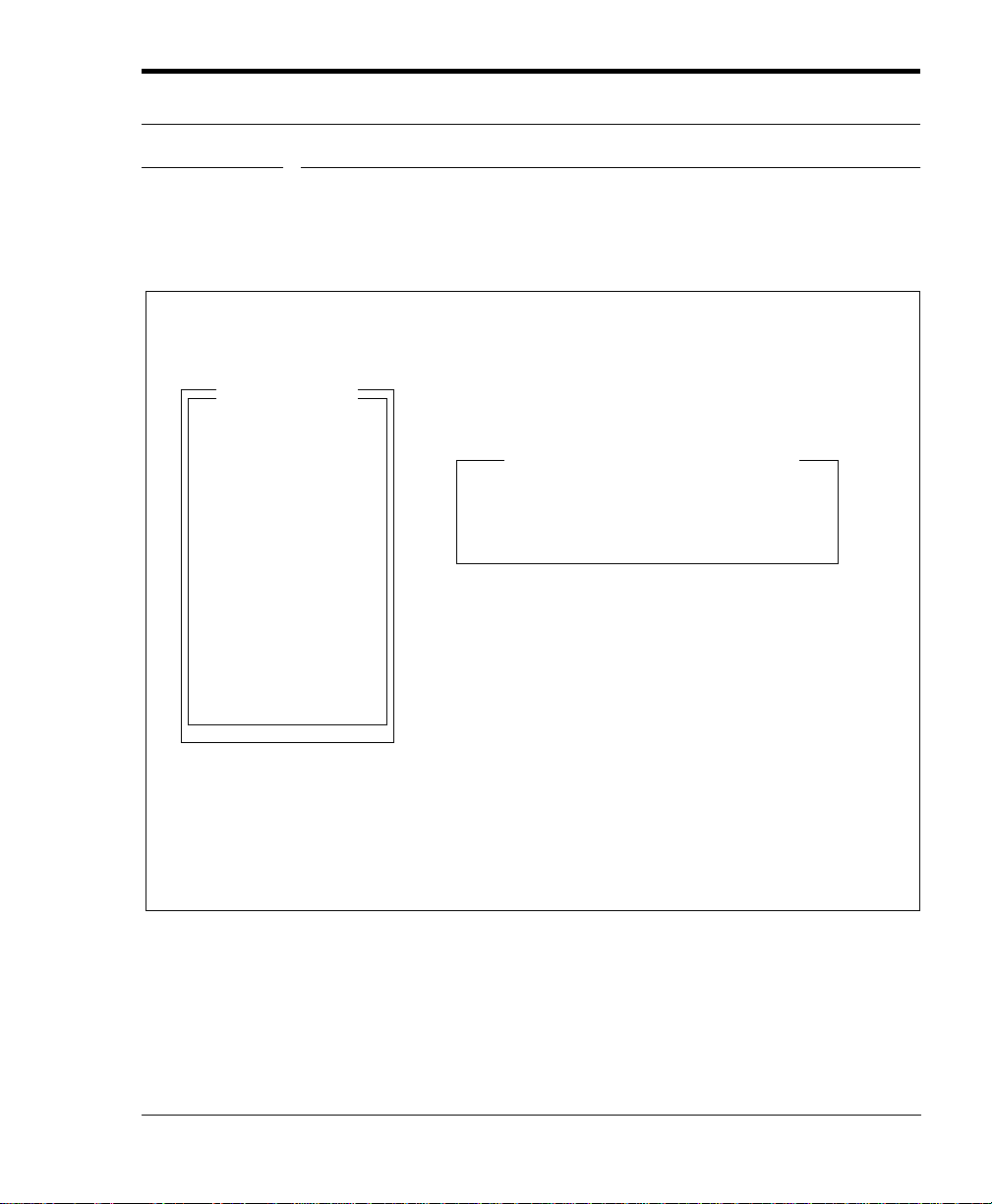
FIGURE 16 - A
Basic Options Menu
Texas Microsystems, Inc. Setup Utility
Model LS486-SX 33MHz BIOS Version 4.0.1.3
Basic Options
Time ................................................ 10:18:28
Date................................................. Aug 30, 1993
Time and Date
Floppy Disks
Fixed Disks
Video Adapter
Keyboard
Shadow RAM
Boot Options
Weekday..........................................Monday
Drive A............................................. 3
Drive B............................................. Not Installed
Hard Disk 1...................................... SCSI Installed
Off
On
Keyboard Configuration Errors
1
/2Inch, 1.44 MB
Hard Disk 2...................................... Not Installed
Video Adapter .................................VGA/EGA
Password Options
Password Edit
Advanced Options
Base Memory..................................640K
Extended Memory...........................3072K
Floating Point Unit........................... Not Present
Park Hard Drive
Flash It!
Fast Boot......................................... No
Boot Drive Sequence ...................... Drive A: then C:
101-Keyboard NumLock..................Off
Password Protection........................ None
Boot Errors: Keyboard:...................On
Floppy:....................... On
Video:......................... On
↑(Previous) ↓ (Next) Enter (execute) Esc (quit/save)
LS486/L486 CPU Card User’s Manual 61
Page 62
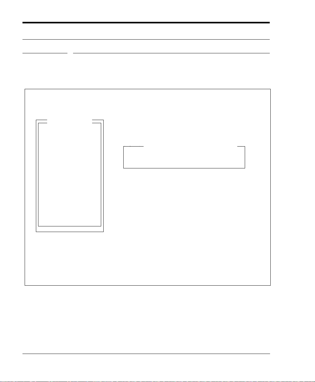
FIGURE 16 - B
Using the Setup Utility
Texas Microsystems, Inc. Setup Utility
Model LS486-SX 33MHz BIOS Version 4.0.1.3
Basic Options
Time ................................................ 10:18:28
Date................................................. Aug 30, 1993
Time and Date
Floppy Disks
Fixed Disks
Video Adapter
Keyboard
Shadow RAM
Boot Options
Weekday..........................................Monday
Drive A............................................. 3
Drive B............................................. Not Installed
Keyboard Typematic Delay
250 msec
1
/2Inch, 1.44 MB
Hard Disk 1...................................... SCSI Installed
Hard Disk 2...................................... Not Installed
Video Adapter .................................VGA/EGA
Password Options
Password Edit
Advanced Options
Base Memory..................................640K
Extended Memory...........................3072K
Floating Point Unit........................... Not Present
Park Hard Drive
Flash It!
Fast Boot......................................... No
Boot Drive Sequence ...................... Drive A: then C:
101-Keyboard NumLock..................Off
Password Protection........................ None
Boot Errors: Keyboard:...................On
Floppy:....................... On
Video:......................... On
↑(Previous) ↓ (Next) Enter (execute) Esc (quit/save)
62 LS486/L486 CPU Card User’s Manual
Page 63
FIGURE 16 - C
Basic Options Menu
Texas Microsystems, Inc. Setup Utility
Model LS486-SX 33MHz BIOS Version 4.0.1.3
Basic Options
Time ................................................ 10:18:28
Date................................................. Aug 30, 1993
Time and Date
Floppy Disks
Fixed Disks
Video Adapter
Keyboard
Shadow RAM
Boot Options
Weekday..........................................Monday
Drive A............................................. 3
Keyboard Typematic Rate
Drive B............................................. Not Installed
24 chars/sec
1
/2Inch, 1.44 MB
Hard Disk 1...................................... SCSI Installed
Hard Disk 2...................................... Not Installed
Video Adapter .................................VGA/EGA
Password Options
Password Edit
Advanced Options
Base Memory..................................640K
Extended Memory...........................3072K
Floating Point Unit........................... Not Present
Park Hard Drive
Flash It!
Fast Boot......................................... No
Boot Drive Sequence ...................... Drive A: then C:
101-Keyboard NumLock..................Off
Password Protection........................ None
Boot Errors: Keyboard:...................On
Floppy:....................... On
Video:......................... On
↑(Previous) ↓ (Next) Enter (execute) Esc (quit/save)
LS486/L486 CPU Card User’s Manual 63
Page 64

Using the Setup Utility
5.1.6 Shadow RAM
This option requires you to specify where the optional ROM-BIOS
code is to be located. When you select this option, a memory map
that displays memory in 16 KByte blocks is displayed. If a ROM is
found within that 16 KByte location, the Setup Utility will display
the word “ROM” or “SHADOW,” where:
• ROM - the system will execute code directly from the
EPROM on the option card, or
• SHADOW - the system will copy the code from the
EPROM into RAM at the same address, allowing code to
run from the RAM on the CPU card (dramatically improving the performance of the system).
A window will also appear to the right of the map. This window displays the following for each option ROM found in the system:
• Starting address of the option ROM
• Length of the option ROM
• Current status (ROM or SHADOW)
This window allows you to toggle between running the option ROM
from the EPROM in which it resides (by selecting ROM), or directing the system to copy it into shadow RAM at power-up (by selecting
SHADOW).
64 LS486/L486 CPU Card User’s Manual
Page 65
FIGURE 17
Basic Options Menu
Texas Microsystems, Inc. Setup Utility
Model LS486-SX 33MHz BIOS Version 4.0.1.3
Basic Options
Time and Date
Floppy Disks
Fixed Disks
Video Adapter
Keyboard
Shadow RAM
Boot Options
Password Options
Password Edit
Advanced Options
Park Hard Drive
Flash It!
Spacebar (change) Enter (execute)
SHADOW
SHADOW
SHADOW
Shadow RAM Definitions
F000-FFFF (CPU BIOS)
E000-EFFF
DC00
D800
D400
D000
CC00
C800
C400
C000
Address: C000:0
Shadow Select
Length: 32K
Status: SHADOW
LS486/L486 CPU Card User’s Manual 65
Page 66

Using the Setup Utility
5.1.7 Boot Options
This function is a series of windows that allows you to set the following items:
• Boot Drive Sequence - you can specify the sequence in
which drives are accessed (useful when attempting to load
an operating system)
• Set status of NumLock key at boot - if a 101-key keyboard
is installed, this option directs the BIOS to enable or disable the NumLock key before booting.
• F ast Booting - When the “Fastboot” feature is enabled, the
BIOS does not perform comprehensive diagnostics at
bootup. This feature enables the machine to boot as
quickly as possible, as it skips the Power-On Self Test
(POST).
Note: A successful normal boot sequence must be performed before
the “Fastboot” option is enabled. Once the correct configuration is
achieved and a normal boot is done, the user may then enter setup
and enable Fastboot. No other changes should be made. If any
changes are to be made, you must again perform a standard boot
after the changes are enacted before you can enable F astboot. You can
press <CTRL-ALT-S> during the boot process to enter the Setup Utility from Fastboot. Note that when this is done, Fastboot is
disabled.
66 LS486/L486 CPU Card User’s Manual
Page 67
FIGURE 18 - A
Basic Options Menu
Texas Microsystems, Inc. Setup Utility
Model LS486-SX 33MHz BIOS Version 4.0.1.3
Basic Options
Time.................................................10:18:28
Date .................................................Aug 30, 1993
Time and Date
Floppy Disks
Fixed Disks
Video Adapter
Keyboard
Shadow RAM
Boot Options
Password Options
Password Edit
Advanced Options
Park Hard Drive
Flash It!
Weekday..........................................Monday
Drive A.............................................3
Drive B.............................................Not Installed
Hard Disk 1......................................SCSI Installed
Hard Disk 2......................................Not Installed
Video Adapter..................................VGA/EGA
Drive A: then C:
Drive C: then A:
Drive A: Only
Drive C: Only
Set Boot Drive Access
1
/2Inch, 1.44 MB
Base Memory...................................640K
Extended Memory............................3072K
Floating Point Unit............................Not Present
Fast Boot..........................................No
Boot Drive Sequence.......................Drive A: then C:
101-Keyboard NumLock...................Off
Password Protection ........................None
Boot Errors: Keyboard:...................On
Floppy:........................On
Video: .........................On
↑(Previous) ↓ (Next) Enter (execute) Esc (quit/save)
LS486/L486 CPU Card User’s Manual 67
Page 68
FIGURE 18 - B
Using the Setup Utility
Texas Microsystems, Inc. Setup Utility
Model LS486-SX 33MHz BIOS Version 4.0.1.3
Basic Options
Time ................................................ 10:18:28
Date................................................. Aug 30, 1993
Time and Date
Floppy Disks
Fixed Disks
Video Adapter
Keyboard
Shadow RAM
Boot Options
Password Options
Password Edit
Advanced Options
Weekday..........................................Monday
Drive A............................................. 3
Set status of NumLock at Boot
Drive B............................................. Not Installed
Hard Disk 1...................................... SCSI Installed
Hard Disk 2...................................... Not Installed
Video Adapter .................................VGA/EGA
Base Memory..................................640K
Off
On
Set Boot Drive Access
Drive A: then C:
Drive C: then A:
Drive A: Only
Drive C: Only
1
/2Inch, 1.44 MB
Extended Memory...........................3072K
Floating Point Unit........................... Not Present
Park Hard Drive
Flash It!
Fast Boot......................................... No
Boot Drive Sequence ...................... Drive A: then C:
101-Keyboard NumLock..................Off
Password Protection........................ None
Boot Errors: Keyboard:...................On
Floppy:....................... On
Video:......................... On
↑(Previous) ↓ (Next) Enter (execute) Esc (quit/save)
68 LS486/L486 CPU Card User’s Manual
Page 69
FIGURE 18 - C
Basic Options Menu
Texas Microsystems, Inc. Setup Utility
Model LS486-SX 33MHz BIOS Version 4.0.1.3
Basic Options
Time.................................................10:18:28
Date .................................................Aug 30, 1993
Time and Date
Floppy Disks
Fixed Disks
Video Adapter
Keyboard
Shadow RAM
Boot Options
Password Options
Password Edit
Advanced Options
Park Hard Drive
Flash It!
Weekday..........................................Monday
Do you want Fast Booting?
Drive A.............................................3
Drive B.............................................Not Installed
Hard Disk 1......................................SCSI Installed
No
Yes
1
/2Inch, 1.44 MB
Hard Disk 2......................................Not Installed
Video Adapter..................................VGA/EGA
Base Memory...................................640K
Extended Memory............................3072K
Floating Point Unit............................Not Present
Fast Boot..........................................No
Boot Drive Sequence.......................Drive A: then C:
101-Keyboard NumLock...................Off
Password Protection ........................None
Boot Errors: Keyboard:...................On
Floppy:........................On
Video: .........................On
↑(Previous) ↓ (Next) Enter (execute) Esc (quit/save)
LS486/L486 CPU Card User’s Manual 69
Page 70

Using the Setup Utility
5.1.8 Password Options
This feature allows you the option of having no password protection,
requiring a password to enter the Setup Utility, or requiring a password to enter Setup and boot. The password is entered from this
menu, and you are prompted to enter it again for verification. The
password may consist of from one to 12 characters. Letters A to Z
(case-sensitive) and numbers 0 to 9 are accepted. If a password is
already entered, you must know the password in order to change it.
Note that Switch SW1-3 will delete all password protection.
WARNING: In addition to deleting any password, SW1-3 will cause
the CPU to load the “default” CMOS settings also. If you haven’t
used the “Flash It!” options to save your settings as the “default,” the
CPU will probably not boot the installed operating system. If this
happens, you will need to reconfigure the CMOS setup to match the
active hardware options (refer to Section 5.1.10 for information on
the Flash-It! options).
70 LS486/L486 CPU Card User’s Manual
Page 71
FIGURE 19 - A
Basic Options Menu
Texas Microsystems, Inc. Setup Utility
Model LS486-SX 33MHz BIOS Version 4.0.1.3
Basic Options
Time.................................................10:18:28
Date .................................................Aug 30, 1993
Time and Date
Floppy Disks
Fixed Disks
Video Adapter
Keyboard
Shadow RAM
Boot Options
Password Options
Password Edit
Advanced Options
Park Hard Drive
Flash It!
Weekday..........................................Monday
Drive A.............................................3
Drive B.............................................Not Installed
Hard Disk 1......................................SCSI Installed
Hard Disk 2......................................Not Installed
None
Setup Only
Setup and System Boot
Password Protect Options
1
/2Inch, 1.44 MB
Video Adapter..................................VGA/EGA
Base Memory...................................640K
Extended Memory............................3072K
Floating Point Unit............................Not Present
Fast Boot..........................................No
Boot Drive Sequence.......................Drive A: then C:
101-Keyboard NumLock...................Off
Password Protection ........................None
Boot Errors: Keyboard:...................On
Floppy:........................On
Video: .........................On
↑(Previous) ↓ (Next) Enter (execute) Esc (quit/save)
LS486/L486 CPU Card User’s Manual 71
Page 72
FIGURE 19 - B
Using the Setup Utility
Texas Microsystems, Inc. Setup Utility
Model LS486-SX 33MHz BIOS Version 4.0.1.3
Basic Options
Time.................................................10:18:28
Date .................................................Aug 30, 1993
Time and Date
Floppy Disks
Fixed Disks
Video Adapter
Keyboard
Shadow RAM
Boot Options
Password Options
Password Edit
Advanced Options
Park Hard Drive
Flash It!
Weekday..........................................Monday
Drive A.............................................3
Password Edit
1
/2Inch, 1.44 MB
Drive B.............................................Not Installed
New Password
Hard Disk 1......................................SCSI Installed
................... *****
Hard Disk 2......................................Not Installed
Video Adapter..................................VGA/EGA
Base Memory...................................640K
Extended Memory............................3072K
Floating Point Unit............................Not Present
Fast Boot..........................................No
Boot Drive Sequence.......................Drive A: then C:
101-Keyboard NumLock...................Off
Password Protection ........................None
Boot Errors: Keyboard:...................On
Floppy:........................On
Video: .........................On
↑(Previous) ↓ (Next) Enter (execute) Esc (quit/save)
72 LS486/L486 CPU Card User’s Manual
Page 73

Basic Options Menu
5.1.9 Park Hard Drive
When enabled, this feature allows you to park the heads on each
hard drive and protect the drives whenever it is necessary to move
or transport the computer. The menu will display a “Continue
Park?” prompt. Press “Yes” to park the hard drives, “No” to discontinue this feature.
Before moving your system, it is recommended that
you park the heads on each hard drive.
NOTICE: Power off the system when done.
Continue Park? Yes No
5.1.10 Flash It!
“Flash It!” permits all selections to be programmed permanently
into BIOS memory. In the event of a CMOS power failure, or whenever SW1-3 is closed, the selections that were current when the
“Flash It!” option was selected will be the new default values that
the system will “load.”
Hard Disk Head Parking Utility
In the event that a new default value prohibits system operation
(including an active password that becomes an unknown), SW1-2
must be closed to invoke the auxiliary BIOS. SW1-3 must also be
closed to load the true factory defaults. After operating the Setup
Utility, you can restore control to the standard BIOS by opening
SW1-2 and SW1-3.
IMPORTANT! While the system is “flashing” BIOS memory, it is
imperative that the reset switch not be pressed and power is not
turned off until the “Flash It” operation has completed. In the event
that the flash operation is interrupted, SW1-2 must be closed to
invoke the auxiliary BIOS and allow the system to be operated. It
will then be necessary to perform another flash operation which,
when successful, will enable SW1-2 to be opened and control
returned to the flashed BIOS.
LS486/L486 CPU Card User’s Manual 73
Page 74

Using the Setup Utility
5.2 Advanced Options
Choosing the “Advanced Options” item from the “Basic Options”
menu will cause a new menu of options to be displayed. We’ll discuss these options in the following sections. The Advanced Options
menu is displayed below.
Advanced Options
Serial Ports
Parallel Ports
Cache
DRAM Speeds
Bus/DMA Speeds
Memory Options
Miscellaneous
Basic Options
74 LS486/L486 CPU Card User’s Manual
Page 75

Advanced Options
5.2.1 Serial Ports
You can select the port addresses for Serial Port 1 (UART1) and
Serial Port 2 (UART2) using this option. The choices are as follows:
• 3F8
• 2F8
• 3E8
• 2E8
• Disabled
Note: Serial Port 1 must use IRQ4, and Serial Port 2 must use
IRQ3. These items are not user-selectable.
If Serial Ports 1 and 2 are given the same base port
address, a window will prompt you to enter a key that will
solve the conflict. You cannot further configure the system
until the serial ports no longer share the same address.
LS486/L486 CPU Card User’s Manual 75
Page 76
FIGURE 20 - A
Using the Setup Utility
Texas Microsystems, Inc. Setup Utility
Model LS486-SX 33MHz BIOS Version 4.0.1.3
Advanced Options
Serial Ports
Parallel Ports
Cache
DRAM Speeds
Bus/DMA Speeds
Memory Options
Miscellaneous
Basic Options
↑(Previous) ↓ (Next) Enter (execute) Esc (quit/save)
Onboard Floppy Controller.............. On
Onboard IDE Interface.................... On
Onboard SCSI ROM ....................... Off
AT Bus Speed ................................. 8 MHz
DMA Speed..................................... 1/2 BUS SPEED
Serial Port .......................................
Serial Port .......................................
Parallel Port.....................................
Flash I/O Port Address.................... 0270H
Internal 486 Cache.......................... Yes
15M -16M Memory.......................... Enable 15M-16M
Top 128K of 32M............................. Enable Top 128K
DRAM Write Wait States................. 0 wait states
DRAM Read Wait States................. 1 wait state
DRAM RAS precharge.................... 2 SYSCLKS
DRAM RAS to CAS timing.............. 0 SYSCLKS
Select Serial Port 1 Address
03F8h, IRQ4
02F8h, IRQ4
03E8h, IRQ4
02E8h, IRQ4
Disabled
76 LS486/L486 CPU Card User’s Manual
Page 77

FIGURE 20 - B
Advanced Options
Texas Microsystems, Inc. Setup Utility
Model LS486-SX 33MHz BIOS Version 4.0.1.3
Advanced Options
Serial Ports
Parallel Ports
Cache
DRAM Speeds
Bus/DMA Speeds
Memory Options
Miscellaneous
Basic Options
↑(Previous) ↓ (Next) Enter (execute) Esc (quit/save)
Onboard Floppy Controller.............. On
Onboard IDE Interface.................... On
Onboard SCSI ROM ....................... Off
AT Bus Speed ................................. 8 MHz
DMA Speed..................................... 1/2 BUS SPEED
Serial Port .......................................
Serial Port .......................................
Parallel Port.....................................
Flash I/O Port Address.................... 0270H
Internal 486 Cache.......................... Yes
15M -16M Memory.......................... Enable 15M-16M
Top 128K of 32M............................. Enable Top 128K
DRAM Write Wait States................. 0 wait states
DRAM Read Wait States................. 1 wait state
DRAM RAS precharge.................... 2 SYSCLKS
DRAM RAS to CAS timing.............. 0 SYSCLKS
Select Serial Port 2 Address
03F8h, IRQ3
02F8h, IRQ3
03E8h, IRQ3
02E8h, IRQ3
Disabled
LS486/L486 CPU Card User’s Manual 77
Page 78
5.2.2 Parallel Ports
FIGURE 21 - A
Using the Setup Utility
Use this feature to select an address for the on-board parallel port.
Once you enable a port address, you may choose between IRQ5,
IRQ7 and NO IRQ. The parallel port can also be configured as standard AT-compatible or bi-directional.
Texas Microsystems, Inc. Setup Utility
Model LS486-SX 33MHz BIOS Version 4.0.1.3
Advanced Options
Serial Ports
Parallel Ports
Cache
DRAM Speeds
Bus/DMA Speeds
Memory Options
Miscellaneous
Basic Options
↑(Previous) ↓ (Next) Enter (execute) Esc (quit/save)
Onboard Floppy Controller.............. On
Onboard IDE Interface.................... On
Onboard SCSI ROM ....................... Off
Select Parallel Port Address
AT Bus Speed ................................. 8 MHz
DMA Speed..................................... 1/2 BUS SPEED
Serial Port .......................................
Serial Port .......................................
Parallel Port.....................................
Flash I/O Port Address.................... 0270H
Internal 486 Cache.......................... Yes
15M -16M Memory.......................... Enable 15M-16M
Top 128K of 32M............................. Enable Top 128K
DRAM Write Wait States................. 0 wait states
DRAM Read Wait States................. 1 wait state
DRAM RAS precharge.................... 2 SYSCLKS
DRAM RAS to CAS timing.............. 0 SYSCLKS
Disabled
03BCh
0378h
0278h
78 LS486/L486 CPU Card User’s Manual
Page 79
FIGURE 21 - B
Advanced Options
Texas Microsystems, Inc. Setup Utility
Model LS486-SX 33MHz BIOS Version 4.0.1.3
Advanced Options
Serial Ports
Parallel Ports
Cache
DRAM Speeds
Bus/DMA Speeds
Memory Options
Miscellaneous
Basic Options
↑(Previous) ↓ (Next) Enter (execute) Esc (quit/save)
Onboard Floppy Controller.............. On
Onboard IDE Interface.................... On
Onboard SCSI ROM ....................... Off
Select Parallel Port IRQ
AT Bus Speed ................................. 8 MHz
DMA Speed..................................... 1/2 BUS SPEED
Serial Port .......................................
Serial Port .......................................
Parallel Port.....................................
Flash I/O Port Address.................... 0270H
Internal 486 Cache.......................... Yes
15M -16M Memory.......................... Enable 15M-16M
Top 128K of 32M............................. Enable Top 128K
DRAM Write Wait States................. 0 wait states
DRAM Read Wait States................. 1 wait state
DRAM RAS precharge.................... 2 SYSCLKS
DRAM RAS to CAS timing.............. 0 SYSCLKS
Select Parallel Port Address
Disabled
No IRQ
03BCh
IRQ5
0378h
IRQ7
0278h
LS486/L486 CPU Card User’s Manual 79
Page 80
FIGURE 21 - C
Using the Setup Utility
Texas Microsystems, Inc. Setup Utility
Model LS486-SX 33MHz BIOS Version 4.0.1.3
Advanced Options
Serial Ports
Parallel Ports
Cache
DRAM Speeds
Bus/DMA Speeds
Memory Options
Miscellaneous
Basic Options
↑(Previous) ↓ (Next) Enter (execute) Esc (quit/save)
Onboard Floppy Controller.............. On
Onboard IDE Interface.................... On
Onboard SCSI ROM ....................... Off
Set Parallel Port Mode
AT Bus Speed ................................. 8 MHz
DMA Speed..................................... 1/2 BUS SPEED
Serial Port .......................................
Serial Port .......................................
Parallel Port.....................................
Flash I/O Port Address.................... 0270H
Internal 486 Cache.......................... Yes
15M -16M Memory.......................... Enable 15M-16M
Top 128K of 32M............................. Enable Top 128K
DRAM Write Wait States................. 0 wait states
DRAM Read Wait States................. 1 wait state
DRAM RAS precharge.................... 2 SYSCLKS
DRAM RAS to CAS timing.............. 0 SYSCLKS
Select Parallel Port IRQ
Select Parallel Port Address
Bidirectional
Compatible
Disabled
No IRQ
03BCh
IRQ5
0378h
IRQ7
0278h
80 LS486/L486 CPU Card User’s Manual
Page 81

Advanced Options
5.2.3 Cache
The LS486S contains no secondary cache, but the internal 8 KByte
CPU cache can be turned on or off via this option. Also, if the cache
is enabled, you can choose to make the shadow RAM area (C0000 to
FFFFF) non-cacheable or cacheable and write-protected.
After responding to these menus, the “Non-Cacheable Memory
Block” window appears, and the “Block Size” column is highlighted.
To increment the block size, press the Page Up key; press the Page
Down key to decrement. The block size options for the LS486 are
512K, 1M, 2M, 4M, 8M and DISABLED.
Once the block size is selected, press the right arrow key to highlight the “Start Addr” column. This column is used to select the
start address for the non-cacheable memory block. As with the
“Block Size” column, press the Page Up key to increment, Page
Down to decrement. The increment unit is the block size selected
earlier.
LS486/L486 CPU Card User’s Manual 81
Page 82
FIGURE 22 - A
Using the Setup Utility
Texas Microsystems, Inc. Setup Utility
Model LS486-SX 33MHz BIOS Version 4.0.1.3
Advanced Options
Serial Ports
Parallel Ports
Cache
DRAM Speeds
Bus/DMA Speeds
Memory Options
Miscellaneous
Basic Options
↑(Previous) ↓ (Next) Enter (execute) Esc (quit/save)
Onboard Floppy Controller.............. On
Onboard IDE Interface.................... On
Onboard SCSI ROM ....................... Off
Use the 486 Internal Cache?
AT Bus Speed ................................. 8 MHz
DMA Speed..................................... 1/2 BUS SPEED
Serial Port .......................................
Serial Port .......................................
Parallel Port.....................................
Flash I/O Port Address.................... 0270H
Internal 486 Cache.......................... Yes
15M -16M Memory.......................... Enable 15M-16M
Top 128K of 32M............................. Enable Top 128K
DRAM Write Wait States................. 0 wait states
DRAM Read Wait States................. 1 wait state
DRAM RAS precharge.................... 2 SYSCLKS
DRAM RAS to CAS timing.............. 0 SYSCLKS
No
Yes
82 LS486/L486 CPU Card User’s Manual
Page 83
FIGURE 22 - B
Advanced Options
Texas Microsystems, Inc. Setup Utility
Model LS486-SX 33MHz BIOS Version 4.0.1.3
Advanced Options
Serial Ports
Parallel Ports
Cache
DRAM Speeds
Bus/DMA Speeds
Memory Options
Miscellaneous
Basic Options
↑(Previous) ↓ (Next) Enter (execute) Esc (quit/save)
Onboard Floppy Controller...............On
Onboard IDE Interface.....................On
Onboard SCSI ROM........................Off
AT Bus Speed..................................8 MHz
DMA Speed .....................................1/2 BUS SPEED
Serial Port........................................
Serial Port........................................
Parallel Port .....................................
Flash I/O Port Address ....................0270H
Internal 486 Cache ..........................Yes
15M -16M Memory...........................Enable 15M-16M
Top 128K of 32M..............................Enable Top 128K
DRAM Write Wait States..................0 wait states
DRAM Read Wait States.................1 wait state
DRAM RAS precharge.....................2 SYSCLKS
DRAM RAS to CAS timing...............0 SYSCLKS
C000H to FFFFFH CACHE
NON Cacheable
Cacheable Write Protected
LS486/L486 CPU Card User’s Manual 83
Page 84
FIGURE 22 - C
Using the Setup Utility
Texas Microsystems, Inc. Setup Utility
Model LS486-SX 33MHz BIOS Version 4.0.1.3
Advanced Options
Serial Ports
Parallel Ports
Cache
DRAM Speeds
Bus/DMA Speeds
Memory Options
Miscellaneous
Basic Options
Pg Up (incr) Pg Down (decr) ↑↓ (select) Enter (execute)
Onboard Floppy Controller.............. On
Onboard IDE Interface .................... On
Onboard SCSI ROM........................ Off
Non-Cacheable Memory Block
AT Bus Speed.................................. 8 MHz
DMA Speed..................................... 1/2 BUS SPEED
Serial Port .......................................
Block Size Start Addr End Addr
Serial Port .......................................
512K 00100000 0017FFFF
Parallel Port.....................................
Flash I/O Port Address.................... 0270H
Internal 486 Cache.......................... Yes
15M -16M Memory..........................Enable 15M-16M
Top 128K of 32M ............................. Enable Top 128K
DRAM Write Wait States................. 0 wait states
DRAM Read Wait States................. 1 wait state
DRAM RAS precharge....................2 SYSCLKS
DRAM RAS to CAS timing .............. 0 SYSCLKS
84 LS486/L486 CPU Card User’s Manual
Page 85
5.2.4 DRAM Speeds
FIGURE 23 - A
Advanced Options
The LS486 chipset allows adjustment of several DRAM (Dynamic
Random Access Memory) timing parameters. DRAM write and read
wait state timing, DRAM RAS precharge timing , and DRAM RAS to
CAS time can all be adjusted separately. Note: A wait state occurs
when the CPU is idle (not processing information). RAS is Row
Address Select, while CAS is Column Address Select. RAS Precharge
is the period of time that RAS is not active. RAS to CAS Time refers
to the period between the time RAS goes active and CAS goes active.
Since RAS and CAS are related to accessing the system memory,
only experienced users should alter the factory default settings.
Texas Microsystems, Inc. Setup Utility
Model LS486-SX 33MHz BIOS Version 4.0.1.3
Advanced Options
Serial Ports
Parallel Ports
Cache
DRAM Speeds
Bus/DMA Speeds
Memory Options
Miscellaneous
Basic Options
↑(Previous) ↓ (Next) Enter (execute) Esc (quit/save)
Onboard Floppy Controller...............On
Onboard IDE Interface.....................On
Onboard SCSI ROM........................Off
Select Dram Write Wait States
AT Bus Speed ..................................8 MHz
DMA Speed......................................1/2 BUS SPEED
Serial Port........................................
Serial Port........................................
Parallel Port......................................
Flash I/O Port Address.....................0270H
Internal 486 Cache ..........................Yes
15M -16M Memory...........................Enable 15M-16M
Top 128K of 32M..............................Enable Top 128K
DRAM Write Wait States..................0 wait states
DRAM Read Wait States..................1 wait state
DRAM RAS precharge.....................2 SYSCLKS
DRAM RAS to CAS timing...............0 SYSCLKS
LS486/L486 CPU Card User’s Manual 85
0 wait states
1 wait state
Page 86
FIGURE 23 - B
Using the Setup Utility
Texas Microsystems, Inc. Setup Utility
Model LS486-SX 33MHz BIOS Version 4.0.1.3
Advanced Options
Serial Ports
Parallel Ports
Cache
DRAM Speeds
Bus/DMA Speeds
Memory Options
Miscellaneous
Basic Options
↑(Previous) ↓ (Next) Enter (execute) Esc (quit/save)
Onboard Floppy Controller.............. On
Onboard IDE Interface .................... On
Onboard SCSI ROM........................ Off
Select Dram Read Wait States
AT Bus Speed.................................. 8 MHz
DMA Speed..................................... 1/2 BUS SPEED
Serial Port .......................................
Serial Port .......................................
Parallel Port.....................................
Flash I/O Port Address.................... 0270H
Internal 486 Cache.......................... Yes
15M -16M Memory..........................Enable 15M-16M
Top 128K of 32M ............................. Enable Top 128K
DRAM Write Wait States................. 0 wait states
DRAM Read Wait States................. 1 wait state
DRAM RAS precharge....................2 SYSCLKS
DRAM RAS to CAS timing .............. 0 SYSCLKS
0 wait states
1 wait state
2 wait states
3 wait states
86 LS486/L486 CPU Card User’s Manual
Page 87
FIGURE 23 - C
Advanced Options
Texas Microsystems, Inc. Setup Utility
Model LS486-SX 33MHz BIOS Version 4.0.1.3
Advanced Options
Serial Ports
Parallel Ports
Cache
DRAM Speeds
Bus/DMA Speeds
Memory Options
Miscellaneous
Basic Options
↑(Previous) ↓ (Next) Enter (execute) Esc (quit/save)
Onboard Floppy Controller...............On
Onboard IDE Interface.....................On
Onboard SCSI ROM........................Off
Select Dram RAS Precharge
AT Bus Speed ..................................8 MHz
DMA Speed......................................1/2 BUS SPEED
Serial Port........................................
Serial Port........................................
Parallel Port......................................
Flash I/O Port Address.....................0270H
Internal 486 Cache ..........................Yes
15M -16M Memory...........................Enable 15M-16M
Top 128K of 32M..............................Enable Top 128K
DRAM Write Wait States..................0 wait states
DRAM Read Wait States..................1 wait state
DRAM RAS precharge.....................2 SYSCLKS
DRAM RAS to CAS timing...............0 SYSCLKS
2 SYSCLKS
3 SYSCLKS
LS486/L486 CPU Card User’s Manual 87
Page 88
FIGURE 23 - D
Using the Setup Utility
Texas Microsystems, Inc. Setup Utility
Model LS486-SX 33MHz BIOS Version 4.0.1.3
Advanced Options
Serial Ports
Parallel Ports
Cache
DRAM Speeds
Bus/DMA Speeds
Memory Options
Miscellaneous
Basic Options
↑(Previous) ↓ (Next) Enter (execute) Esc (quit/save)
Onboard Floppy Controller.............. On
Onboard IDE Interface.................... On
Onboard SCSI ROM ....................... Off
Select Dram RAS to CAS time
AT Bus Speed ................................. 8 MHz
DMA Speed..................................... 1/2 BUS SPEED
Serial Port .......................................
Serial Port .......................................
Parallel Port.....................................
Flash I/O Port Address.................... 0270H
Internal 486 Cache.......................... Yes
15M -16M Memory.......................... Enable 15M-16M
Top 128K of 32M............................. Enable Top 128K
DRAM Write Wait States................. 0 wait states
DRAM Read Wait States................. 1 wait state
DRAM RAS precharge.................... 2 SYSCLKS
DRAM RAS to CAS timing.............. 0 SYSCLKS
0 SYSCLKS
1 SYSCLKS
88 LS486/L486 CPU Card User’s Manual
Page 89

Advanced Options
5.2.5 Bus/DMA Speed
These options allow you to select the proper bus and DMA (Direct
Memory Access) speeds. Direct memory access allows data to be
transferred between peripheral devices and internal memory without intervention from the CPU.
The bus speed can be selected as 8, 10 or 12 MHz. Although 8 MHz
is the AT-compatible standard, many newer peripherals will run at
faster speeds. However, when selecting the bus speed, be aware of
peripheral equipment speed limitations.
The DMA speed can be selected to be equal to, or half of, the system
bus speed. The standard AT-compatible speed is one-half the standard 8 MHz bus speed, i.e. 4 MHz. However, many newer peripherals will run at faster speeds.
The Chips and Technologies 82C206 controller can be configured to
fine-tune performance. Wait states are inserted by the 82C206 Integrated Peripherals Controller. The system will cause the 82C206 to
assert a “not ready” condition on IOCHRDY (I/O Channel Ready) for
the number of wait states selected in the 82C206 Read/Write Cycle
field. The “CT206 Read/Write W ait State” setting allows the setting
of wait states for I/O operations to the CT206 chip. Wait states for 8bit and 16-bit DMA (Direct Memory Access) may be controlled independently to allow user-customizing.
Note: Texas Micro recommends setting the “Bus Speed” option to 8
MHz and the “DMA Speed” option to “1/2 Bus Speed.” From this
starting point, you can increase Bus/DMA speeds to desired settings
unless you experience system problems. Then, you can decrease the
settings until the problem is resolved.
LS486/L486 CPU Card User’s Manual 89
Page 90
FIGURE 24 - A
Using the Setup Utility
Texas Microsystems, Inc. Setup Utility
Model LS486-SX 33MHz BIOS Version 4.0.1.3
Advanced Options
Serial Ports
Parallel Ports
Cache
DRAM Speeds
Bus/DMA Speeds
Memory Options
Miscellaneous
Basic Options
↑(Previous) ↓ (Next) Enter (execute) Esc (quit/save)
Onboard Floppy Controller.............. On
Onboard IDE Interface .................... On
Onboard SCSI ROM........................ Off
AT Bus Speed.................................. 8 MHz
DMA Speed..................................... 1/2 BUS SPEED
Serial Port .......................................
Serial Port .......................................
Parallel Port.....................................
Flash I/O Port Address.................... 0270H
Internal 486 Cache.......................... Yes
15M -16M Memory..........................Enable 15M-16M
Top 128K of 32M ............................. Enable Top 128K
DRAM Write Wait States................. 0 wait states
DRAM Read Wait States................. 1 wait state
DRAM RAS precharge....................2 SYSCLKS
DRAM RAS to CAS timing .............. 0 SYSCLKS
AT Bus Speed
8 MHz
10 MHz
12 MHz
90 LS486/L486 CPU Card User’s Manual
Page 91
FIGURE 24 - B
Advanced Options
Texas Microsystems, Inc. Setup Utility
Model LS486-SX 33MHz BIOS Version 4.0.1.3
Advanced Options
Serial Ports
Parallel Ports
Cache
DRAM Speeds
Bus/DMA Speeds
Memory Options
Miscellaneous
Basic Options
↑(Previous) ↓ (Next) Enter (execute) Esc (quit/save)
Onboard Floppy Controller.............. On
Onboard IDE Interface .................... On
Onboard SCSI ROM........................ Off
AT Bus Speed.................................. 8 MHz
DMA Speed..................................... 1/2 BUS SPEED
Serial Port .......................................
Serial Port .......................................
Parallel Port.....................................
Flash I/O Port Address.................... 0270H
Internal 486 Cache.......................... Yes
15M -16M Memory..........................Enable 15M-16M
Top 128K of 32M ............................. Enable Top 128K
DRAM Write Wait States................. 0 wait states
DRAM Read Wait States................. 1 wait state
DRAM RAS precharge....................2 SYSCLKS
DRAM RAS to CAS timing .............. 0 SYSCLKS
DMA Speed
1/2 Bus Speed (4.00 MHz)
AT Bus Speed
Bus Speed (8.00 MHz)
8 MHz
10 MHz
12 MHz
LS486/L486 CPU Card User’s Manual 91
Page 92
FIGURE 24 - C
Using the Setup Utility
Texas Microsystems, Inc. Setup Utility
Model LS486-SX 33MHz BIOS Version 4.0.1.3
Advanced Options
Serial Ports
Parallel Ports
Cache
DRAM Speeds
Bus/DMA Speeds
Memory Options
Miscellaneous
Basic Options
↑(Previous) ↓ (Next) Enter (execute) Esc (quit/save)
Onboard Floppy Controller.............. On
Onboard IDE Interface.....................On
Onboard SCSI ROM........................ Off
CT206 Read/Write Waitstates
AT Bus Speed..................................8 MHz
DMA Speed..................................... 1/2 BUS SPEED
Serial Port........................................
Serial Port........................................
Parallel Port.....................................
Flash I/O Port Address.................... 0270H
Internal 486 Cache.......................... Yes
15M -16M Memory..........................Enable 15M-16M
Top 128K of 32M .............................Enable Top 128K
DRAM Write Wait States................. 0 wait states
DRAM Read Wait States.................1 wait state
DRAM RAS precharge....................2 SYSCLKS
DRAM RAS to CAS timing ..............0 SYSCLKS
1 WAIT STATE
2 WAIT STATES
3 WAIT STATES
4 WAIT STATES
92 LS486/L486 CPU Card User’s Manual
Page 93
FIGURE 24 - D
Advanced Options
Texas Microsystems, Inc. Setup Utility
Model LS486-SX 33MHz BIOS Version 4.0.1.3
Advanced Options
Serial Ports
Parallel Ports
Cache
DRAM Speeds
Bus/DMA Speeds
Memory Options
Miscellaneous
Basic Options
↑(Previous) ↓ (Next) Enter (execute) Esc (quit/save)
Onboard Floppy Controller.............. On
Onboard IDE Interface .................... On
Onboard SCSI ROM........................ Off
AT Bus Speed.................................. 8 MHz
DMA Speed..................................... 1/2 BUS SPEED
Serial Port .......................................
Serial Port .......................................
Parallel Port.....................................
Flash I/O Port Address.................... 0270H
Internal 486 Cache.......................... Yes
15M -16M Memory..........................Enable 15M-16M
Top 128K of 32M ............................. Enable Top 128K
DRAM Write Wait States................. 0 wait states
DRAM Read Wait States................. 1 wait state
DRAM RAS precharge....................2 SYSCLKS
DRAM RAS to CAS timing .............. 0 SYSCLKS
8 Bit DMA Waitstates
1 WAIT STATE
2 WAIT STATES
3 WAIT STATES
4 WAIT STATES
LS486/L486 CPU Card User’s Manual 93
Page 94
FIGURE 24 - E
Using the Setup Utility
Texas Microsystems, Inc. Setup Utility
Model LS486-SX 33MHz BIOS Version 4.0.1.3
Advanced Options
Serial Ports
Parallel Ports
Cache
DRAM Speeds
Bus/DMA Speeds
Memory Options
Miscellaneous
Basic Options
↑(Previous) ↓ (Next) Enter (execute) Esc (quit/save)
Onboard Floppy Controller...............On
Onboard IDE Interface.....................On
Onboard SCSI ROM........................Off
AT Bus Speed ..................................8 MHz
DMA Speed......................................1/2 BUS SPEED
Serial Port........................................
Serial Port........................................
Parallel Port......................................
Flash I/O Port Address.....................0270H
Internal 486 Cache ..........................Yes
15M -16M Memory...........................Enable 15M-16M
Top 128K of 32M..............................Enable Top 128K
DRAM Write Wait States..................0 wait states
DRAM Read Wait States..................1 wait state
DRAM RAS precharge.....................2 SYSCLKS
DRAM RAS to CAS timing...............0 SYSCLKS
16 Bit DMA Waitstates
1 WAIT STATE
2 WAIT STATES
3 WAIT STATES
4 WAIT STATES
94 LS486/L486 CPU Card User’s Manual
Page 95

Advanced Options
5.2.6 Memory Options
Set Base Memory Size
The LS486 base memory can be set to either 640 KBytes (the usual
amount of memory for an AT-compatible computer) or 512 KBytes.
Since a few add-on cards are mapped to the 512 - 640 KByte region,
this option allows you to configure the system to run these cards in
the 512 - 640 KByte area.
15M to 16M Memory
If the on-board memory is 16 MBytes or greater, this option also
allows you to create a “hole” in the 15 MByte to 16 MByte region.
This hole is sometimes used by UNIX add-in cards that expect to be
mapped to this region. However, if a card on the AT bus must use
this region, this option will allow this configuration without the
removal of memory SIMM’s.
Top 128K of 32M
Another option designed for UNIX users allows the enabling or disabling of the top 128 KBytes of memory. Most versions of UNIX will
perform dynamic memory sizing, which can cause UNIX to “alias”
memory up to the maximum 4 GByte end of memory. This can occur
with the ETEQ ET6000 chip set when the LS486 is configured with
32 MBytes of on-board memory. By disabling the top 128 KBytes of
the on-board RAM, you can prevent UNIX from “wrapping around”
the memory map and sizing the memory incorrectly.
LS486/L486 CPU Card User’s Manual 95
Page 96
FIGURE 25 - A
Using the Setup Utility
Texas Microsystems, Inc. Setup Utility
Model LS486-SX 33MHz BIOS Version 4.0.1.3
Advanced Options
Serial Ports
Parallel Ports
Cache
DRAM Speeds
Bus/DMA Speeds
Memory Options
Miscellaneous
Basic Options
↑(Previous) ↓ (Next) Enter (execute) Esc (quit/save)
Onboard Floppy Controller.............. On
Onboard IDE Interface.................... On
Onboard SCSI ROM ....................... Off
AT Bus Speed ................................. 8 MHz
DMA Speed..................................... 1/2 BUS SPEED
Serial Port .......................................
Serial Port .......................................
Parallel Port.....................................
Flash I/O Port Address.................... 0270H
Internal 486 Cache.......................... Yes
15M -16M Memory.......................... Enable 15M-16M
Top 128K of 32M............................. Enable Top 128K
DRAM Write Wait States................. 0 wait states
DRAM Read Wait States................. 1 wait state
DRAM RAS precharge.................... 2 SYSCLKS
DRAM RAS to CAS timing.............. 0 SYSCLKS
Set Base Memory Size
640K Base Memory
512K Base Memory
96 LS486/L486 CPU Card User’s Manual
Page 97
FIGURE 25 - B
Advanced Options
Texas Microsystems, Inc. Setup Utility
Model LS486-SX 33MHz BIOS Version 4.0.1.3
Advanced Options
Serial Ports
Parallel Ports
Cache
DRAM Speeds
Bus/DMA Speeds
Memory Options
Miscellaneous
Basic Options
↑(Previous) ↓ (Next) Enter (execute) Esc (quit/save)
Onboard Floppy Controller.............. On
Onboard IDE Interface.................... On
Onboard SCSI ROM ....................... Off
AT Bus Speed ................................. 8 MHz
DMA Speed..................................... 1/2 BUS SPEED
Serial Port .......................................
Serial Port .......................................
Parallel Port.....................................
Flash I/O Port Address.................... 0270H
Internal 486 Cache.......................... Yes
15M -16M Memory.......................... Enable 15M-16M
Top 128K of 32M............................. Enable Top 128K
DRAM Write Wait States................. 0 wait states
DRAM Read Wait States................. 1 wait state
DRAM RAS precharge.................... 2 SYSCLKS
DRAM RAS to CAS timing.............. 0 SYSCLKS
15M to 16M Memory
Enable 15M-16M
Disable 15M-16M
LS486/L486 CPU Card User’s Manual 97
Page 98
FIGURE 25 - C
Using the Setup Utility
Texas Microsystems, Inc. Setup Utility
Model LS486-SX 33MHz BIOS Version 4.0.1.3
Advanced Options
Serial Ports
Parallel Ports
Cache
DRAM Speeds
Bus/DMA Speeds
Memory Options
Miscellaneous
Basic Options
↑(Previous) ↓ (Next) Enter (execute) Esc (quit/save)
Onboard Floppy Controller.............. On
Onboard IDE Interface .................... On
Onboard SCSI ROM........................ Off
AT Bus Speed.................................. 8 MHz
DMA Speed..................................... 1/2 BUS SPEED
Serial Port .......................................
Serial Port .......................................
Parallel Port.....................................
Flash I/O Port Address.................... 0270H
Internal 486 Cache.......................... Yes
15M -16M Memory..........................Enable 15M-16M
Top 128K of 32M ............................. Enable Top 128K
DRAM Write Wait States................. 0 wait states
DRAM Read Wait States................. 1 wait state
DRAM RAS precharge....................2 SYSCLKS
DRAM RAS to CAS timing .............. 0 SYSCLKS
Top 128K of 32M
Enable Top 128K
Disable Top 128K
98 LS486/L486 CPU Card User’s Manual
Page 99
5.2.7 Miscellaneous
FIGURE 26 - A
Advanced Options
This selection will offer additional option menus only if certain nonstandard “BIOS extensions” have been installed in BIOS memory.
One such extension is the Serial Redirection BIOS. When installed,
the Miscellaneous selection will permit selection of a serial port,
baud rate and other options pertaining to the BIOS extension.
Any installed BIOS extension will be accompanied with documentation covering options available in “Miscellaneous.”
Texas Microsystems, Inc. Setup Utility
Model LS486-SX 33MHz BIOS Version 4.0.1.3
Advanced Options
Serial Ports
Parallel Ports
Cache
DRAM Speeds
Bus/DMA Speeds
Memory Options
Miscellaneous
Basic Options
↑(Previous) ↓ (Next) Enter (execute) Esc (quit/save)
Onboard Floppy Controller.............. On
Onboard IDE Interface .................... On
Onboard SCSI ROM........................ Off
AT Bus Speed.................................. 8 MHz
DMA Speed..................................... 1/2 BUS SPEED
Serial Port .......................................
Serial Port .......................................
Parallel Port.....................................
Flash I/O Port Address.................... 0270H
Internal 486 Cache.......................... Yes
15M -16M Memory..........................Enable 15M-16M
Top 128K of 32M ............................. Enable Top 128K
DRAM Write Wait States................. 0 wait states
DRAM Read Wait States................. 1 wait state
DRAM RAS precharge....................2 SYSCLKS
DRAM RAS to CAS timing .............. 0 SYSCLKS
LS486/L486 CPU Card User’s Manual 99
Redirection COM Port
DISABLED
COM1
COM2
COM1 & COM2
Page 100
FIGURE 26 - B
Using the Setup Utility
Texas Microsystems, Inc. Setup Utility
Model LS486-SX 33MHz BIOS Version 4.0.1.3
Advanced Options
Serial Ports
Parallel Ports
Cache
DRAM Speeds
Bus/DMA Speeds
Memory Options
Miscellaneous
Basic Options
↑(Previous) ↓ (Next) Enter (execute) Esc (quit/save)
Onboard Floppy Controller.............. On
Onboard IDE Interface .................... On
Onboard SCSI ROM........................ Off
AT Bus Speed.................................. 8 MHz
DMA Speed..................................... 1/2 BUS SPEED
Serial Port .......................................
Serial Port .......................................
Parallel Port.....................................
Flash I/O Port Address.................... 0270H
Internal 486 Cache.......................... Yes
15M -16M Memory..........................Enable 15M-16M
Top 128K of 32M ............................. Enable Top 128K
DRAM Write Wait States................. 0 wait states
DRAM Read Wait States................. 1 wait state
DRAM RAS precharge....................2 SYSCLKS
DRAM RAS to CAS timing .............. 0 SYSCLKS
Redirection Baud Rate
4800
9600
19200
100 LS486/L486 CPU Card User’s Manual
 Loading...