

Page 1
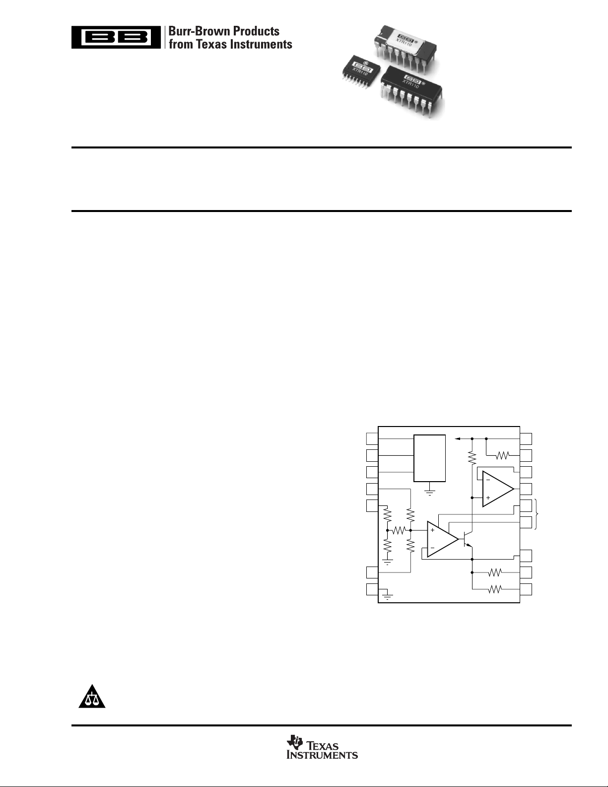
SBOS141A – JANUARY 1984 – REVISED AUGUST 2003
PRECISION VOLTAGE-TO-CURRENT
CONVERTER/TRANSMITTER
XTR110
FEATURES
● 4mA TO 20mA TRANSMITTER
● SELECTABLE INPUT/OUTPUT RANGES:
0V to +5V, 0V to +10V Inputs
0mA to 20mA, 5mA to 25mA Outputs
Other Ranges
● 0.005% MAX NONLINEARITY, 14 BIT
● PRECISION +10V REFERENCE OUTPUT
● SINGLE SUPPLY OPERATION
● WIDE SUPPLY RANGE: 13.5V to 40V
DESCRIPTION
The XTR110 is a precision voltage-to-current converter
designed for analog signal transmission. It accepts inputs of
0 to 5V or 0 to 10V and can be connected for outputs of 4
to 20mA, 0 to 20mA, 5 to 25mA and many other commonly
used ranges.
A precision on-chip metal film resistor network provides
input scaling and current offsetting. An internal 10V voltage
reference can be used to drive external circuitry.
The XTR110 is available in 16-pin plastic DIP, ceramic DIP
and SOL-16 surface-mount packages. Commercial and industrial temperature range models are available.
APPLICATIONS
● INDUSTRIAL PROCESS CONTROL
● PRESSURE/TEMPERATURE TRANSMITTERS
● CURRENT-MODE BRIDGE EXCITATION
● GROUNDED TRANSDUCER CIRCUITS
● CURRENT SOURCE REFERENCE FOR DATA
ACQUISITION
● PROGRAMMABLE CURRENT SOURCE FOR
TEST EQUIPMENT
● POWER PLANT/ENERGY SYSTEM
MONITORING
+V
V
REF
V
REF
V
REF
V
IN1
V
Common
Force
Sense
Adjust
(10V)
V
REF
(5V)
IN2
15
12
11
4
3
In
R
R
5
2
+10V
Reference
1
R
3
R
5
R
4
A
2
1
R
8
A
R
R
16
1
13
14
7
6
8
10
9
CC
Source
Resistor
Source
Sense
Gate
Drive
Offset
(zero)
Adjust
Span
Adjust
4mA
Span
16mA
Span
R
9
2
7
6
Please be aware that an important notice concerning availability, standard warranty, and use in critical applications of
Texas Instruments semiconductor products and disclaimers thereto appears at the end of this data sheet.
All trademarks are the property of their respective owners.
PRODUCTION DATA information is current as of publication date.
Products conform to specifications per the terms of Texas Instruments
standard warranty. Production processing does not necessarily include
testing of all parameters.
Copyright © 1984-2003, Texas Instruments Incorporated
www.ti.com
Page 2
SPECIFICATIONS
ELECTRICAL
At T
= +25°C and V
A
PARAMETER CONDITIONS MIN TYP MAX MIN TYP MAX UNITS
TRANSMITTER
Transfer Function
Input Range: V
Current, I
O
Nonlinearity 16mA/20mA Span
Offset Current, I
Initial
vs Temperature
vs Supply, V
Span Error I
Initial
vs Temperature
vs Supply, V
Output Resistance From Drain of FET (Q
Input Resistance V
Dynamic Response
Settling Time To 0.1% of Span 15 * µs
Slew Rate 1.3 * mA/µs
VOLTAGE REFERENCE
Output Voltage +9.95 +10 +10.05 +9.98 * +10.02 V
vs Temperature 35 50 15 30 ppm/°C
vs Supply, V
vs Output Current Load Regulation 0.0005 0.01 * * %/mA
vs Time 100 * ppm/1k hrs
Trim Range –0.100 +0.25 * * V
Output Current Specified Performance 10 * mA
POWER SUPPLY
Input Voltage, V
Quiescent Current Excluding I
TEMPERATURE RANGE
Specification:AG, BG –40 +85 * * °C
Operating:AG, BG –55 +125 * * °C
KP, KU –25 +85 °C
= +24V and R
CC
= 250Ω**, unless otherwise specified.
L
XTR110AG, KP, KU XTR110BG
(5)
IN1
V
IN2
OS
CC
CC
Specified Performance 0 +10 * * V
Specified Performance 0 +5 * * V
Specified Performance
Derated Performance
IO = 4mA
(1)
(1)
(1)
= 20mA
O
(1)
(1)
(1)
IN1
V
IN2
V
REF
(1)
(1)
(2)
(1)
)
EXT
420* *mA
040* *mA
(3)
In 19 * kΩ
IO = 10 [(V
0.01 0.025 0.002 0.005 % of Span
0.2 0.4 0.02 0.1 % of Span
0.0003 0.005 * 0.003 % of Span/°C
0.0005 0.005 * * % of Span/V
0.3 0.6 0.05 0.2 % of Span
0.0025 0.005 0.0009 0.003 % of Span/°C
0.003 0.005 * * % of Span/V
10 x 10
27 * kΩ
22 * kΩ
In/16) + (V
REF
9
/4) + (V
IN1
IN2
/2)] /R
SPAN
* Ω
To 0.01% of Span 20 * µs
CC
CC
Line Regulation 0.0002 0.005 * * %/V
+13.5 +40 * * V
O
3 4.5 * * mA
KP, KU 0 +70 °C
* Specifications same as AG/KP grades. ** Specifications apply to the range of RL shown in Typical Performance Curves.
NOTES: (1) Including internal reference. (2) Span is the change in output current resulting from a full-scale change in input voltage. (3) Within compliance range limited
by (+V
– 2V) +VDS required for linear operation of the FET. (4) For V
CC
be damaged. See section, “Input Voltage Range”.
ABSOLUTE MAXIMUM RATINGS
Power Supply, +VCC............................................................................ 40V
Input Voltage, V
See text regarding safe negative input voltage range.
, V
, V
IN1
IN2
....................................................... +V
REF IN
Storage Temperature Range: A, B ................................ –55°C to +125°C
K, U ..................................–40°C to +85°C
Lead Temperature
(soldering, 10s) G, P ................................................................... 300°C
(wave soldering, 3s) U ................................................................ 260°C
Output Short-Circuit Duration, Gate Drive
and V
Output Current Using Internal 50Ω Resistor ................................... 40mA
Force................................ Continuous to common and +V
REF
2
adjustment circuit see Figure 3. (5) For extended I
REF
ELECTROSTATIC
CC
CC
www.ti.com
This integrated circuit can be damaged by ESD. Texas Instruments
recommends that all integrated circuits be handled with appropriate
precautions. Failure to observe proper handling and installation procedures can cause damage.
ESD damage can range from subtle performance degradation to
complete device failure. Precision integrated circuits may be more
susceptible to damage because very small parametric changes could
cause the device not to meet its published specifications.
DISCHARGE SENSITIVITY
drive circuit see Figure 4. (5) Unit may
REF
XTR110
SBOS141A
Page 3
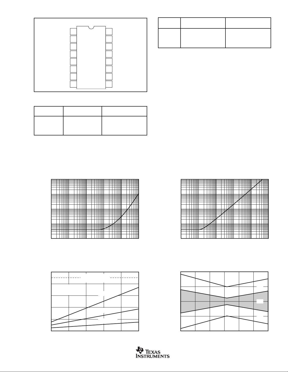
PIN CONFIGURATION
Top View
Source Resistor
Common
V
In
REF
V
(10V)
IN1
V
(5V)
IN2
Zero Adjust
Zero Adjust
Span Adjust
1
2
3
4
5
6
7
8
16
+V
15
V
REF
14
Gate Drive
13
Source Sense
12
V
REF
11
V
REF
10
4mA Span
9
16mA Span
CC
Force
Sense
Adjust
ORDERING INFORMATION
PRODUCT PACKAGE RANGE
XTR110AG 16-Pin Ceramic DIP –40°C to +85°C
XTR110BG 16-Pin Ceramic DIP –40°C to +85°C
XTR110KP 16-Pin Plastic DIP 0°C to +70°C
XTR110KU SOL-16 Surface-Mount 0°C to +70°C
TEMPERATURE
PACKAGE INFORMATION
PRODUCT PACKAGE NUMBER
PACKAGE DRAWING
XTR110AG 16-Pin Ceramic DIP 109
XTR110BG 16-Pin Ceramic DIP 109
XTR110KP 16-Pin Plastic DIP 180
XTR110KU SOL-16 Surface-Mount 211
NOTE: (1) For detailed drawing and dimension table, please see end of data
sheet, or Appendix C of Burr-Brown IC Data Book.
(1)
TYPICAL PERFORMANCE CURVES
TA = +25°C, VCC = 24VDC, RL = 250Ω, unless otherwise noted.
V
LINE REGULATION vs FREQUENCY
10
1
(%/V)
CC
0.1
/∆ V
REF
∆ V
0.01
0.001
1 10 100 1k 10k 100k
100
80
60
40
Above Ambient (°C)
20
Junction Temperature Rise
REF
JUNCTION TEMPERATURE RISE
vs V
Max. TJ = +175°C
= 70°C/W
JA
Ripple Frequency (Hz)
OUTPUT CURRENT
REF
Max. Temp. Rise
for +85°C Ambient
VCC = +40V
V
= +24V
CC
VCC = +15V
I
POWER SUPPLY REGULATION vs FREQUENCY
O
10
1
0.1
(% of span/V)
CC
/∆ V
O
0.01
∆ I
0.001
1 10 100 1k 10k 100k
Ripple Frequency (Hz)
TOTAL OUTPUT ERROR vs TEMPERATURE
2
1
0
Error (% of span)
–1
AG
BG
AG
0
XTR110
SBOS141A
280104
Output Current (mA)
V
REF
(I
has minimal effect on TJ)
OUT
–2
6
–40
–200 20406080
Temperature (°C)
www.ti.com
3
Page 4
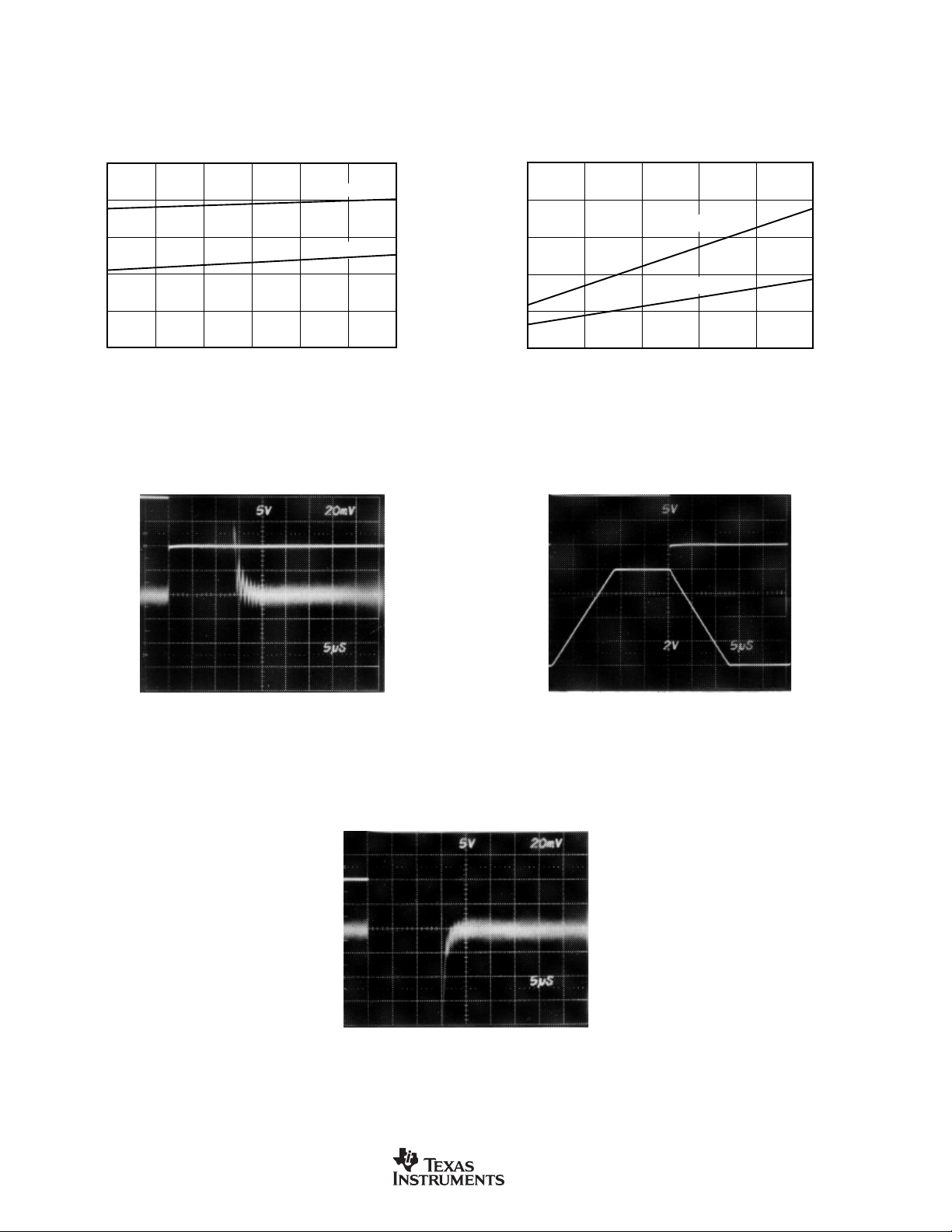
TYPICAL PERFORMANCE CURVES (CONT)
At TA = +25°C, VCC = 24VDC, RL = 250Ω, unless otherwise noted.
5
4
)
O
3
2
(mA) (excluding I
CC
I
1
0
–40
–200 20406080
V
IN
0V
0V
Error
I
O
(0.01% of
Span/Box)
I
vs TEMPERATURE
CC
IO = 20mA
IO = 4mA
Temperature (°C)
SETTLING TIME WITH NEG VIN STEP
+V
vs V
L
CC
I
= 20mA
O MAX
I
= 40mA
O MAX
(V)
CC
2500
2000
1500
(Ω)
L
R
1000
500
0
MAXIMUM R
20 3515 4025 30
PULSE RESPONSE
V
IN
0V
I
O
into
500Ω
0V
SETTLING TIME WITH POS VIN STEP
V
IN
0V
0V
Error
I
O
(0.01% of
Span/Box)
4
www.ti.com
XTR110
SBOS141A
Page 5
APPLICATIONS INFORMATION
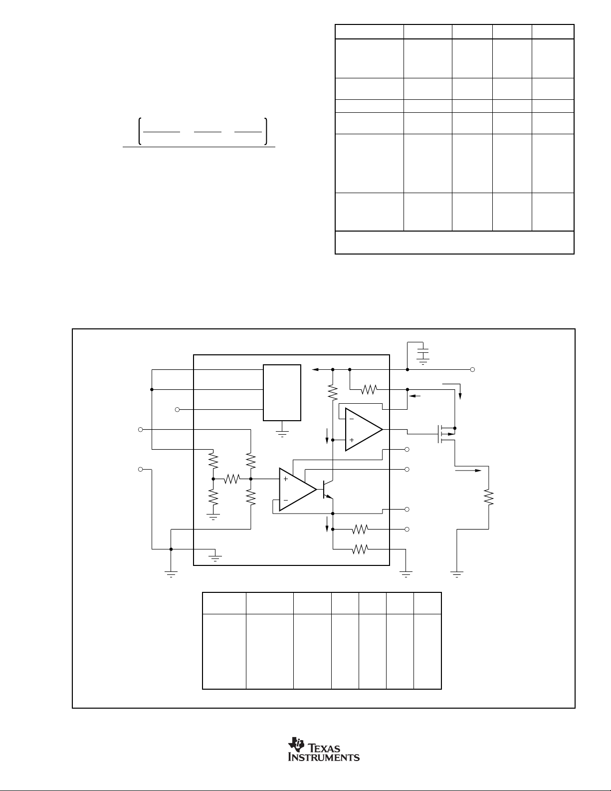
Figure 1 shows the basic connections required for 0 to 10V
input and 4 to 20mA output. Other input voltage and output
current ranges require changes in connections of pins 3, 4, 5,
9 and 10 as shown in the table of Figure 1.
The complete transfer function of the XTR110 is:
(V
)16(V
10 + +
REF IN
IO = (1)
R
is the internal 50Ω resistor, R9, when connected as
SPAN
shown in Figure 1. An external R
different output current ranges as described later.
EXTERNAL TRANSISTOR
An external pass transistor, Q
Figure 1. This transistor conducts the output signal current.
A P-channel MOSFET transistor is recommended. It must
have a voltage rating equal or greater than the maximum
power supply voltage. Various recommended types are shown
in Table I.
)
(V
IN1
4
R
SPAN
can be connected for
SPAN
, is required as shown in
EXT
)
IN2
2
MANUFACTURER PART NO. BV
Ferranti ZVP1304A 40V 20V TO-92
International
Rectifier IRF9513 60V 20V TO-220
Motorola MTP8P08 80V 20V TO-220
RCA RFL1P08 80V 20V TO-39
Siliconix VP0300B 30V 40V TO-39
(preferred) VP0300L 30V 40V TO-92
Supertex VP1304N2 40V 20V TO-220
NOTE: (1) BV
breakdown voltage.
ZVP1304B 40V 20V TO-39
ZVP1306A 60V 20V TO-92
ZVP1306B 60V 20V TO-39
RFT2P08 80V 20V TO-220
VP0300M 30V 40V TO-237
VP0808B 80V 40V TO-39
VP0808L 80V 40V TO-92
VP0808M 80V 40V TO-237
VP1304N3 40V 20V TO-92
VP1306N2 60V 20V TO-220
VP1306N3 60V 20V TO-92
—Drain-source breakdown voltage. BVGS—Gate-source
DSS
DSS
(1)
BV
GS
(1)
PACKAGE
TABLE I. Available P-Channel MOSFETs.
V
0 to 10V
CC
+
1µF
Short
Connection
(see text)
Zero
Adjust
Span Adjust
4mA Span
16mA Span
+V
13.5 to 40V
I
O
Q
EXT
P-Channel
MOSFET
(see text)
I
O
4 to 20mA
CC
R
L
(250Ω typ)
+V
Force
15
Sense
12
V
11
REF
Adj.
4
IN
3
5
2
15kΩ
R
R
1
R
2
5
16.25kΩ
5kΩ
INPUT OUTPUT
RANGE (V) RANGE (mA) PIN 3 PIN 4 PIN 5 PIN 9 PIN 10
0-10 0-20 Com Input Com Com Com
2-10 4-20 Com Input Com Com Com
0-10 4-20 +10V Ref Input Com Com Open
0-10 5-25 +10V Ref Input Com Com Com
0-5 0-20 Com Com Input Com Com
1-5 4-20 Com Com Input Com Com
0-5 4-20 +10V Ref Com Input Com Open
0-5 5-25 +10V Ref Com Input Com Com
Reference
R
3
20kΩ
R
4
10kΩ
+10V
IO/10
IO/10
R
8
500Ω
R
R
6
R
6250Ω
7
1562.5Ω
9
50Ω
16
1
13
14
7
6
8
10
9
FIGURE 1. Basic Circuit Connection.
XTR110
SBOS141A
www.ti.com
5
Page 6

If the supply voltage, +VCC, exceeds the gate-to-source
breakdown voltage of Q
(drain of Q
) is broken, Q
EXT
source breakdown voltage is lower than +VCC, Q
, and the output connection
EXT
could fail. If the gate-to-
EXT
EXT
can be
protected with a 12V zener diode connected from gate to
source.
Two PNP discrete transistors (Darlington-connected) can be
used for Q
—see Figure 2. Note that an additional capaci-
EXT
tor is required for stability. Integrated Darlington transistors
are not recommended because their internal base-emitter
resistors cause excessive error.
XTR110
+V
CC
16
2
47nF
1
13
14
0.047µF
2N2907
etc.
TIP30B
etc.
I
OUT
R
L
TRANSISTOR DISSIPATION
Maximum power dissipation of Q
depends on the power
EXT
supply voltage and full-scale output current. Assuming that
the load resistance is low, the power dissipated by Q
P
= (+VCC) I
MAX
FS
EXT
is:
(2)
The transistor type and heat sinking must be chosen according to the maximum power dissipation to prevent overheating. See Table II for general recommendations.
PACKAGE TYPE ALLOWABLE POWER DISSIPATION
TO-92 Lowest: Use minimum supply and at +25°C.
TO-237 Acceptable: Trade-off supply and temperature.
TO-39 Good: Adequate for majority of designs.
TO-220 Excellent: For prolonged maximum stress.
TO-3 Use if hermetic package is required.
TABLE II. External Transistor Package Type and
Dissipation.
INPUT VOLTAGE RANGE
The internal op amp A1 can be damaged if its non-inverting
input (an internal node) is pulled more than 0.5V below
common (0V). This could occur if input pins 3, 4 or 5 were
driven with an op amp whose output could swing negative
under abnormal conditions. The voltage at the input of A1 is:
(V
)16(V
VA1 = + + (3)
REF IN
)4(V
IN1
IN2
)
2
Common
FIGURE 2. Q
V
Using PNP Transistors.
EXT
V
REF
V
REF
V
REF
NOTE: (1) R
range, set R
REF
R
20kΩ
Adjust Range
±5% Optimum
gives higher resolution with reduced
S
= 0Ω for larger range.
S
Force
Sense
Adjust
R
S
+V
CC
15
12
11
(1)
XTR110
16
Common
2
FIGURE 3. Optional Adjustment of Reference Voltage.
+10V
REF
Q
REF
Force
Sense
15
12
XTR110
16
2
+V
CC
This voltage should not be allowed to go more negative than
–0.5V. If necessary, a clamp diode can be connected from
the negative-going input to common to clamp the input
voltage.
COMMON (Ground)
Careful attention should be directed toward proper connection of the common (grounds). All commons should
be joined at one point as close to pin 2 of the XTR110 as
possible. The exception is the I
return. It can be
OUT
returned to any point where it will not modulate the
common at pin 2.
VOLTAGE REFERENCE
The reference voltage is accurately regulated at pin 12
(V
REF SENSE
6
). To preserve accuracy, any load including pin
www.ti.com
For 100mA with V
40V use 2N3055 for Q
CC
up to
REF
.
FIGURE 4. Increasing Reference Current Drive.
3 should be connected to this point. The circuit in Figure 3
shows adjustment of the voltage reference.
The current drive capability of the XTR110’s internal reference is 10mA. This can be extended if desired by adding an
external NPN transistor shown in Figure 4.
OFFSET (ZERO) ADJUSTMENT
The offset current can be adjusted by using the potentiometer, R1, shown in Figure 5. Set the input voltage to zero and
then adjust R1 to give 4mA at the output. For spans starting
XTR110
SBOS141A
Page 7

0V
to
+10V
15
12
3
4
5
Offset
Adjust
6
R
XTR110
7
1
2
9
8
R
4
R
2
Span Adjust
16
R
3
1µF Tantalum
1
13
G
14
S
D
4mA to
20mA Out
Third Wire
24V
R
L
250Ω
R
20
+
–
1V
to
+5V
Out
(mA)
O
Output Current, I
–2.5
15
16mA Span
10
5
Zero Adjust ±1.8% Optimum
4mA Offset
0246810
= 100kΩ
1
R
= 100kΩ
2
R
= 49.9kΩ
3
R
= 31.6Ω
4
Input Voltage, V
Span Adjust ±0.45%
as shown
(V)
IN1
FIGURE 6. Zero and Span of 0V to +10V Input, 4mA to
20mA Output Configuration (see Figure 5).
FIGURE 5. Offset and Span Adjustment Circuit for 0V to
+10V Input, 4mA to 20mA Output.
at 0mA, the following special procedure is recommended:
set the input to a small nonzero value and then adjust R1 to
the proper output current. When the input is zero the output
will be zero. Figures 6 and 7 show graphically how offset is
adjusted.
SPAN ADJUSTMENT
The span is adjusted at the full-scale output current using the
potentiometer, R2, shown in Figure 5. This adjustment is
interactive with the offset adjustment, and a few iterations
may be necessary. For the circuit shown, set the input
voltage to +10V full scale and adjust R2 to give 20mA fullscale output. Figures 6 and 7 show graphically how span is
adjusted.
The values of R2, R3, and R4 for adjusting the span are
determined as follows: choose R4 in series to slightly decrease the span; then choose R2 and R3 to increase the span
to be adjustable about the center value.
LOW TEMPERATURE COEFFICIENT OPERATION
Although the precision resistors in the XTR110 track within
1ppm/°C, the output current depends upon the absolute
temperature coefficient (TC) of any one of the resistors, R6,
R7, R8, and R9. Since the absolute TC of the output current
can have 20ppm/°C, maximum, the TC of the output current
can have 20ppm/°C drift. For low TC operation, zero TC
resistors can be substituted for either the span resistors (R
or R7) or for the source resistor (R9) but not both.
20
See values in Figure 6.
(mA)
15
O
10
Output Current, I
5
0246810
In addition, connect
pins 9 and 10 together.
20mA Span
Zero Adjust
0mA Offset
Input Voltage, V
Span Adjust
(V)
IN1
FIGURE 7. Zero and Span of 0V to +10VIN, 0mA to 20mA
Output Configuration (see Figure 5).
EXTENDED SPAN
For spans beyond 40mA, the internal 50Ω resistor (R9) may
be replaced by an external resistor connected between pins
13 and 16.
Its value can be calculated as follows:
R
= R9 (Span
EXT
OLD
/Span
NEW
Since the internal thin-film resistors have a 20% absolute
value tolerance, measure R9 before determining the final
6
value of R
. Self-heating of R
EXT
can cause nonlinearity.
EXT
Therefore, choose one with a low TC and adequate power
rating. See Figure 10 for application.
)
XTR110
SBOS141A
www.ti.com
7
Page 8

TYPICAL APPLICATIONS
The XTR110 is ideal for a variety of applications requiring
high noise immunity current-mode signal transmission. The
precision +10V reference can be used to excite bridges and
transducers. Selectable ranges make it very useful as a
precision programmable current source. The compact design
15
12
11
4
3
5
2
3
Offset
Adjust
V
IN
A
4
R
9
15kΩ
R
10
1kΩ
A
3
R
R
2MΩ
5
20kΩ
and low price of the XTR110 allow versatility with a
minimum of external components and design engineering
expense.
Figures 8 through 10 show typical applications of the
XTR110.
+15V
16
+10V
Reference
R
402Ω
1
13
14
7
6
8
10
9
6
R
1
2Ω
T
1
R
7
4.75kΩ
R
200Ω
8
Fine Trim
RH 50kΩ
Course Trim
Span
Adjust
T
3
R
2kΩ
I
(mA)
200
O
0
–200
FIGURE 8. ±200mA Current Pump.
A
2
A
1
4
T
2
R
4.99Ω
2
I
O
–15V
, R2: Low TC resistors to dissipate 0.32W continuous power.
R
1
R
, R10, R11: 10-turn trimpots for greatest sensitivity.
8
V
(V)
IN
105
For other current ranges, scale both resistors proportionately.
R
, R7: Low TC resistors.
6
A
- A4: 1/4 LM324 (powered by ±15V).
1
T
: International Rectifier IR9513
1
T
: International Rectifier IR513
2
T
: International Rectifier IRFF9113
3
(1)
.
(1)
.
(1)
.
NOTE: (1) Or other adequate power rating MOS transistor.
8
www.ti.com
XTR110
SBOS141A
Page 9

Isolation Barrier
Isolated Power
Supply (722)
–15V +15V +15V–15V
7
8
0 to –10V
15
16
ISO122
FIGURE 9. Isolated 4mA to 20mA Channel.
+15V
1µF
15
12
3
XTR110
4
5
16
1
13
S
G
14
2
9
+24V
4mA to 20mA Out
D
R
L
V
L
15
12
4
0V to +10V
See extended span section.
XTR110
3
5
2
9
FIGURE 10. 0A to 10A Output Voltage-to-Current Converter.
R
16
13
14
G
EXT
0.1Ω
0A to
S
10A Out
D
XTR110
SBOS141A
www.ti.com
9
Page 10

PACKAGE DRAWINGS
10
www.ti.com
XTR110
SBOS141A
Page 11

PACKAGE DRAWINGS (CONT)
XTR110
SBOS141A
www.ti.com
11
Page 12

PACKAGE OPTION ADDENDUM
www.ti.com
12-Sep-2006
PACKAGING INFORMATION
Orderable Device Status
(1)
Package
Type
Package
Drawing
Pins Package
Qty
Eco Plan
XTR110AD OBSOLETE XCEPT Y 0 TBD Call TI Call TI
XTR110AG NRND CDIP SB JD 16 24 Green (RoHS &
no Sb/Br)
XTR110BG NRND CDIP SB JD 16 24 Green (RoHS &
no Sb/Br)
XTR110KP ACTIVE PDIP N 16 25 Green (RoHS &
no Sb/Br)
XTR110KPG4 ACTIVE PDIP N 16 25 Green (RoHS &
no Sb/Br)
XTR110KU ACTIVE SOIC DW 16 48 Green (RoHS &
no Sb/Br)
XTR110KU/1K ACTIVE SOIC DW 16 1000 Green (RoHS &
no Sb/Br)
XTR110KU/1KG4 ACTIVE SOIC DW 16 1000 Green(RoHS &
no Sb/Br)
(1)
The marketing status values are defined as follows:
ACTIVE: Product device recommended for new designs.
LIFEBUY: TI has announced that the device will be discontinued, and a lifetime-buy period is in effect.
NRND: Not recommended for new designs. Device is in production to support existing customers, but TI does not recommend using this part in
a new design.
PREVIEW: Device has been announced but is not in production. Samples may or may not be available.
OBSOLETE: TI has discontinued the production of the device.
(2)
Lead/Ball Finish MSL Peak Temp
Call TI N / A for Pkg Type
Call TI N / A for Pkg Type
CU NIPDAU N / A for Pkg Type
CU NIPDAU N / A for Pkg Type
CU NIPDAU Level-3-260C-168 HR
CU NIPDAU Level-3-260C-168 HR
CU NIPDAU Level-3-260C-168 HR
(3)
(2)
Eco Plan - The planned eco-friendly classification: Pb-Free (RoHS), Pb-Free (RoHS Exempt), or Green (RoHS & no Sb/Br) - please check
http://www.ti.com/productcontent for the latest availability information and additional product content details.
TBD: The Pb-Free/Green conversion plan has not been defined.
Pb-Free (RoHS): TI's terms "Lead-Free" or "Pb-Free" mean semiconductor products that are compatible with the current RoHS requirements
for all 6 substances, including the requirement that lead not exceed 0.1% by weight in homogeneous materials. Where designed to be soldered
at high temperatures, TI Pb-Free products are suitable for use in specified lead-free processes.
Pb-Free (RoHS Exempt): This component has a RoHS exemption for either 1) lead-based flip-chip solder bumps used between the die and
package, or 2) lead-based die adhesive used between the die and leadframe. The component is otherwise considered Pb-Free (RoHS
compatible) as defined above.
Green (RoHS & no Sb/Br): TI defines "Green" to mean Pb-Free (RoHS compatible), and free of Bromine (Br) and Antimony (Sb) based flame
retardants (Br or Sb do not exceed 0.1% by weight in homogeneous material)
(3)
MSL, Peak Temp. -- The Moisture Sensitivity Level rating according to the JEDEC industry standard classifications, and peak solder
temperature.
Important Information and Disclaimer:The information provided on this page represents TI's knowledge and belief as of the date that it is
provided. TI bases its knowledge and belief on information provided by third parties, and makes no representation or warranty as to the
accuracy of such information. Efforts are underway to better integrate information from third parties. TI has taken and continues to take
reasonable steps to provide representative and accurate information but may not have conducted destructive testing or chemical analysis on
incoming materials and chemicals. TI and TI suppliers consider certain information to be proprietary, and thus CAS numbers and other limited
information may not be available for release.
In no event shall TI's liability arising out of such information exceed the total purchase price of the TI part(s) at issue in this document sold by TI
to Customer on an annual basis.
Addendum-Page 1
Page 13

Page 14

Page 15

Page 16

IMPORTANT NOTICE
Texas Instruments Incorporated and its subsidiaries (TI) reserve the right to make corrections, modifications,
enhancements, improvements, and other changes to its products and services at any time and to discontinue
any product or service without notice. Customers should obtain the latest relevant information before placing
orders and should verify that such information is current and complete. All products are sold subject to TI’s terms
and conditions of sale supplied at the time of order acknowledgment.
TI warrants performance of its hardware products to the specifications applicable at the time of sale in
accordance with TI’s standard warranty. Testing and other quality control techniques are used to the extent TI
deems necessary to support this warranty . Except where mandated by government requirements, testing of all
parameters of each product is not necessarily performed.
TI assumes no liability for applications assistance or customer product design. Customers are responsible for
their products and applications using TI components. To minimize the risks associated with customer products
and applications, customers should provide adequate design and operating safeguards.
TI does not warrant or represent that any license, either express or implied, is granted under any TI patent right,
copyright, mask work right, or other TI intellectual property right relating to any combination, machine, or process
in which TI products or services are used. Information published by TI regarding third-party products or services
does not constitute a license from TI to use such products or services or a warranty or endorsement thereof.
Use of such information may require a license from a third party under the patents or other intellectual property
of the third party, or a license from TI under the patents or other intellectual property of TI.
Reproduction of information in TI data books or data sheets is permissible only if reproduction is without
alteration and is accompanied by all associated warranties, conditions, limitations, and notices. Reproduction
of this information with alteration is an unfair and deceptive business practice. TI is not responsible or liable for
such altered documentation.
Resale of TI products or services with statements different from or beyond the parameters stated by TI for that
product or service voids all express and any implied warranties for the associated TI product or service and
is an unfair and deceptive business practice. TI is not responsible or liable for any such statements.
Following are URLs where you can obtain information on other Texas Instruments products and application
solutions:
Products Applications
Amplifiers amplifier.ti.com Audio www.ti.com/audio
Data Converters dataconverter.ti.com Automotive www.ti.com/automotive
DSP dsp.ti.com Broadband www.ti.com/broadband
Interface interface.ti.com Digital Control www.ti.com/digitalcontrol
Logic logic.ti.com Military www.ti.com/military
Power Mgmt power.ti.com Optical Networking www.ti.com/opticalnetwork
Microcontrollers microcontroller.ti.com Security www.ti.com/security
Low Power Wireless www.ti.com/lpw Telephony www.ti.com/telephony
Video & Imaging www.ti.com/video
Wireless www.ti.com/wireless
Mailing Address: Texas Instruments
Post Office Box 655303 Dallas, Texas 75265
Copyright 2006, Texas Instruments Incorporated
 Loading...