

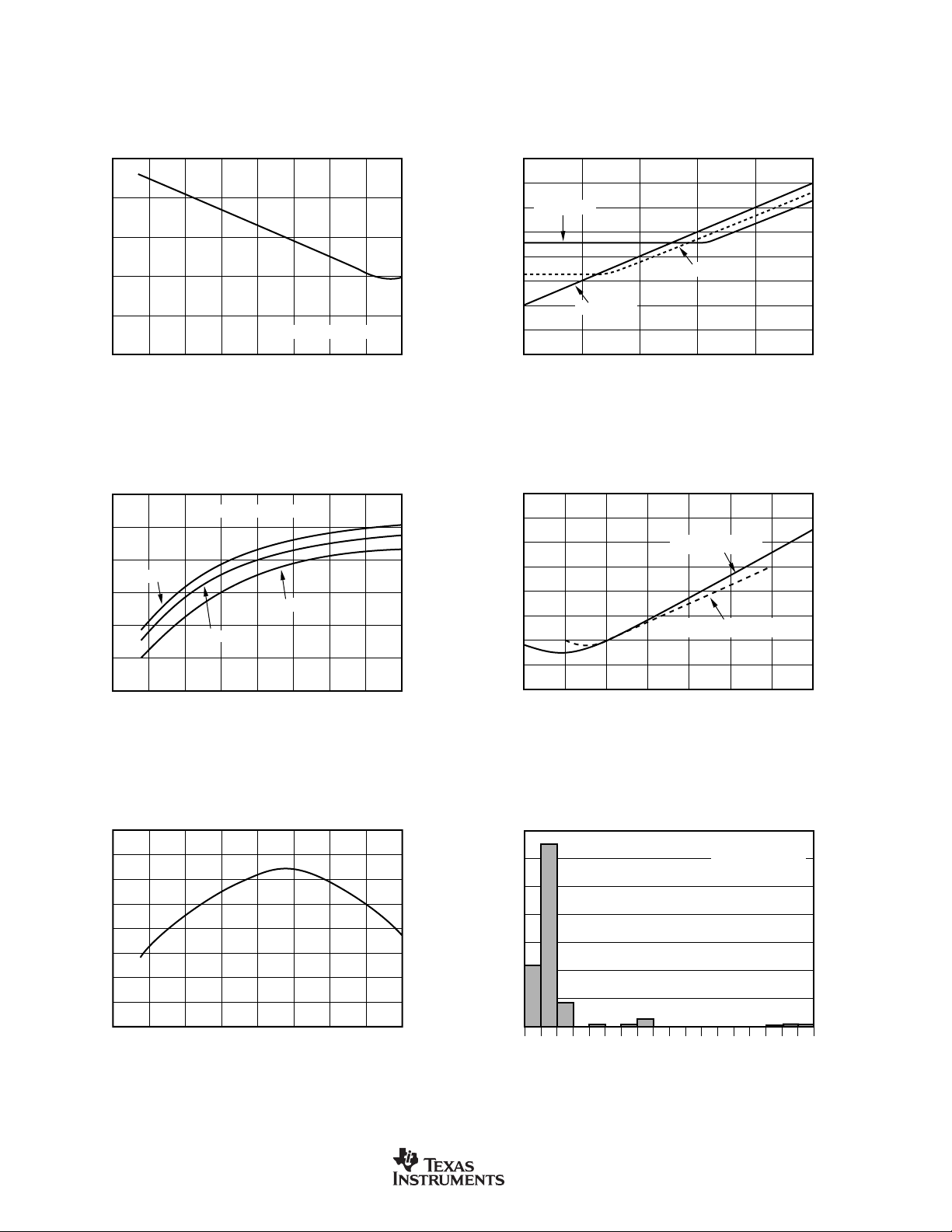
XTR106
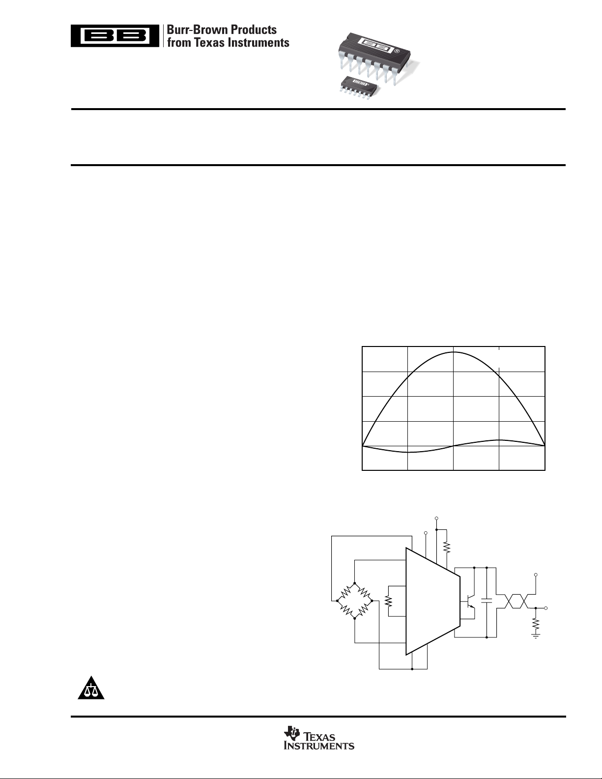
BRIDGE NONLINEARITY CORRECTION
USING XTR106
0
Bridge Output (mV)
10
2.0
1.5
1.0
0.5
0
–0.5
Uncorrected
Bridge Output
Corrected
5
Nonlinearity (%)
X
TR
1
06
SBOS092A – JUNE 1998 – REVISED NOVEMBER 2003
4-20mA CURRENT TRANSMITTER
with Bridge Excitation and Linearization
XTR106
FEATURES
● LOW TOTAL UNADJUSTED ERROR
● 2.5V, 5V BRIDGE EXCITATION REFERENCE
● 5.1V REGULATOR OUTPUT
● LOW SPAN DRIFT: ±25ppm/°C max
● LOW OFFSET DRIFT: 0.25µV/°C
● HIGH PSR: 110dB min
● HIGH CMR: 86dB min
● WIDE SUPPLY RANGE: 7.5V to 36V
● 14-PIN DIP AND SO-14 SURFACE-MOUNT
DESCRIPTION
The XTR106 is a low cost, monolithic 4-20mA, twowire current transmitter designed for bridge sensors. It
provides complete bridge excitation (2.5V or 5V reference), instrumentation amplifier, sensor linearization,
and current output circuitry. Current for powering additional external input circuitry is available from the
V
pin.
REG
The instrumentation amplifier can be used over a wide
range of gain, accommodating a variety of input signal
types and sensors. Total unadjusted error of the complete current transmitter, including the linearized bridge,
is low enough to permit use without adjustment in many
applications. The XTR106 operates on loop power supply voltages down to 7.5V.
Linearization circuitry provides second-order correction
to the transfer function by controlling bridge excitation
voltage. It provides up to a 20:1 improvement in
nonlinearity, even with low cost transducers.
The XTR106 is available in 14-pin plastic DIP and
SO-14 surface-mount packages and is specified for the
–40°C to +85°C temperature range. Operation is from
–55°C to +125°C.
Please be aware that an important notice concerning availability, standard warranty, and use in critical applications of
Texas Instruments semiconductor products and disclaimers thereto appears at the end of this data sheet.
All trademarks are the property of their respective owners.
PRODUCTION DATA information is current as of publication date.
Products conform to specifications per the terms of Texas Instruments
standard warranty. Production processing does not necessarily include
testing of all parameters.
APPLICATIONS
● PRESSURE BRIDGE TRANSMITTERS
● STRAIN GAGE TRANSMITTERS
● TEMPERATURE BRIDGE TRANSMITTERS
● INDUSTRIAL PROCESS CONTROL
● SCADA REMOTE DATA ACQUISITION
● REMOTE TRANSDUCERS
● WEIGHING SYSTEMS
● ACCELEROMETERS
5V
www.ti.com
V
(5.1V)
REG
2.5V
V
V
REF
REF
5
R
Lin
Polarity
LIN
7.5V to 36V
I
OUT
4-20mA
+
I
G
RET
XTR106
–
R
Copyright © 1998-2003, Texas Instruments Incorporated
V
PS
V
O
R
L

SPECIFICATIONS
At TA = +25°C, V+ = 24V, and TIP29C external transistor, unless otherwise noted.
XTR106P, U XTR106PA, UA
PARAMETER CONDITIONS MIN TYP MAX MIN TYP MAX UNITS
OUTPUT
Output Current Equation I
Output Current, Specified Range 4 20 ✻✻mA
Over-Scale Limit I
Under-Scale Limit I
ZERO OUTPUT
(1)
Initial Error ±5 ±25 ✻ ±50 µA
vs Temperature T
vs Supply Voltage, V+ V+ = 7.5V to 36V 0.04 0.2 ✻✻ µA/V
vs Common-Mode Voltage
vs V
(IO) 0.8 ✻ µA/mA
REG
Noise: 0.1Hz to 10Hz i
(CMRR)
OVER
UNDER
I
ZERO
O
I
= 0, I
REG
I
+ I
REF
= 0 1 1.6 2.2 ✻✻✻ mA
REF
= 2.5mA 2.9 3.4 4 ✻✻✻ mA
REG
VIN = 0V, RG = ∞ 4 ✻ mA
= –40°C to +85°C ±0.07 ±0.9 ✻✻ µA/°C
A
VCM = 1.1V to 3.5V
n
(5)
SPAN
Span Equation (Transconductance) S
Untrimmed Error Full Scale (V
vs Temperature
Nonlinearity: Ideal Input
INPUT
Offset Voltage V
vs Temperature T
vs Supply Voltage, V+ V+ = 7.5V to 36V ±0.1 ±3 ✻✻ µV/V
vs Common-Mode Voltage, RTI CMRR V
Common-Mode Range
Input Bias Current I
vs Temperature T
Input Offset Current I
vs Temperature T
Impedance: Differential Z
Noise: 0.1Hz to 10Hz V
VOLTAGE REFERENCES
(2)
(3)
(4)
(5)
Common-Mode 5 || 10 ✻ GΩ || pF
(5)
TA = –40°C to +85°C ±3 ±25 ✻✻ ppm/°C
Full Scale (VIN) = 50mV ±0.001 ±0.01 ✻✻ %
OS
V
CM
OS
IN
= –40°C to +85°C ±0.25 ±1.5 ✻ ±3 µV/°C
A
CM
B
= –40°C to +85°C20 ✻ pA/°C
A
= –40°C to +85°C5 ✻ pA/°C
A
n
Lin Polarity Connected
to V
Initial: 2.5V Reference V
5V Reference V
Accuracy V
vs Temperature T
vs Supply Voltage, V+ V+ = 7.5V to 36V ±5 ±20 ✻✻ ppm/V
vs Load I
Noise: 0.1Hz to 10Hz 10 ✻ µVp-p
(5)
V
REG
Accuracy ±0.02 ±0.1 ✻✻ V
vs Temperature T
vs Supply Voltage, V+ V+ = 7.5V to 36V 1 ✻ mV/V
Output Current I
Output Impedance I
LINEARIZATION
R
(external) Equation R
LIN
K
Linearization Factor K
LIN
(6)
2.5 2.5 ✻ V
REF
55✻ V
V
REF
REG
REG
LIN
LIN
REF
= –40°C to +85°C ±20 ±35 ✻ ±75 ppm/°C
A
REF
= –40°C to +85°C ±0.3 ✻ mV/°C
A
REG
Accuracy ±1 ±5 ✻✻ %
vs Temperature T
Max Correctable Sensor Nonlinearity B V
= –40°C to +85°C ±50 ±100 ✻✻ ppm/°C
A
) = 50mV ±0.05 ±0.2 ✻ ±0.4 %
IN
VCM = 2.5V ±50 ±100 ✻ ±250 µV
= 1.1V to 3.5V
, R
REG
(5)
= 0
LIN
= 2.5V or 5V ±0.05 ±0.25 ✻ ±0.5 %
= 0mA to 2.5mA 60 ✻ ppm/mA
= 0mA to 2.5mA 80 ✻ Ω
V
= 5V 6.645 ✻ kΩ
REF
V
= 2.5V 9.905 ✻ kΩ
REF
= 5V ±5 ✻ % of V
REF
V
= 2.5V –2.5, +5 ✻ % of V
REF
POWER SUPPLY V+
Specified +24 ✻ V
Voltage Range +7.5 +36 ✻✻V
TEMPERATURE RANGE
Specification –40 +85 ✻✻°C
Operating –55 +125 ✻✻°C
Storage –55 +125 ✻✻°C
Thermal Resistance
14-Pin DIP 80 ✻ °C/W
θ
JA
SO-14 Surface Mount 100 ✻ °C/W
✻ Specification same as XTR106P, XTR106U.
NOTES: (1) Describes accuracy of the 4mA low-scale offset current. Does not include input amplifier effects. Can be trimmed to zero. (2) Does not include initial
error or TCR of gain-setting resistor, R
measured with respect to I
pin. (6) See “Linearization” text for detailed explanation. VFS = full-scale VIN.
RET
. (3) Increasing the full-scale input range improves nonlinearity. (4) Does not include Zero Output initial error. (5) Voltage
G
IO = VIN • (40/RG) + 4mA, VIN in Volts, RG in Ω
24 28 30 ✻✻✻ mA
0.02 ✻ µA/V
0.035 ✻ µAp-p
S = 40/R
G
✻ A/V
±10 ±50 ✻ ±100 µV/V
1.1 3.5 ✻✻V
525 ✻ 50 nA
±0.2 ±3 ✻ ±10 nA
0.1 || 1 ✻ GΩ || pF
0.6 ✻ µVp-p
5.1 ✻ V
See Typical Curves ✻ mA
R
= K
LIN
4B
• , K
LIN
1 – 2B
in Ω, B is nonlinearity relative to V
LIN
FS
A
Ω
FS
FS
2
www.ti.com
XTR106
SBOS092A
PIN CONFIGURATION
Top View DIP and SOIC
1
V
REG
–
2
V
IN
3
R
G
4
R
G
+
5
V
IN
6
I
RET
7
I
O
14
13
12
11
10
9
8
V
5
REF
V
2.5
REF
Lin Polarity
R
LIN
V+
B (Base)
E (Emitter)
PACKAGE/ORDERING INFORMATION
For the most current package and ordering information, see
the Package Option Addendum at the end of this data sheet.
ABSOLUTE MAXIMUM RATINGS
Power Supply, V+ (referenced to IO pin).......................................... 40V
Input Voltage, V
Storage Temperature Range ....................................... –55°C to +125°C
Lead Temperature (soldering, 10s) .............................................. +300°C
Output Current Limit ............................................................... Continuous
Junction Temperature ................................................................... +165°C
NOTE: (1) Stresses above these ratings may cause permanent damage.
Exposure to absolute maximum conditions for extended periods may degrade
device reliability.
+
–
, VIN (referenced to I
IN
(1)
pin) ......................... 0V to V+
RET
ELECTROSTATIC
DISCHARGE SENSITIVITY
This integrated circuit can be damaged by ESD. Texas Instruments recommends that all integrated circuits be handled with
appropriate precautions. Failure to observe proper handling
and installation procedures can cause damage.
ESD damage can range from subtle performance degradation to complete device failure. Precision integrated circuits
may be more susceptible to damage because very small
parametric changes could cause the device not to meet its
published specifications.
XTR106
SBOS092A
www.ti.com
3
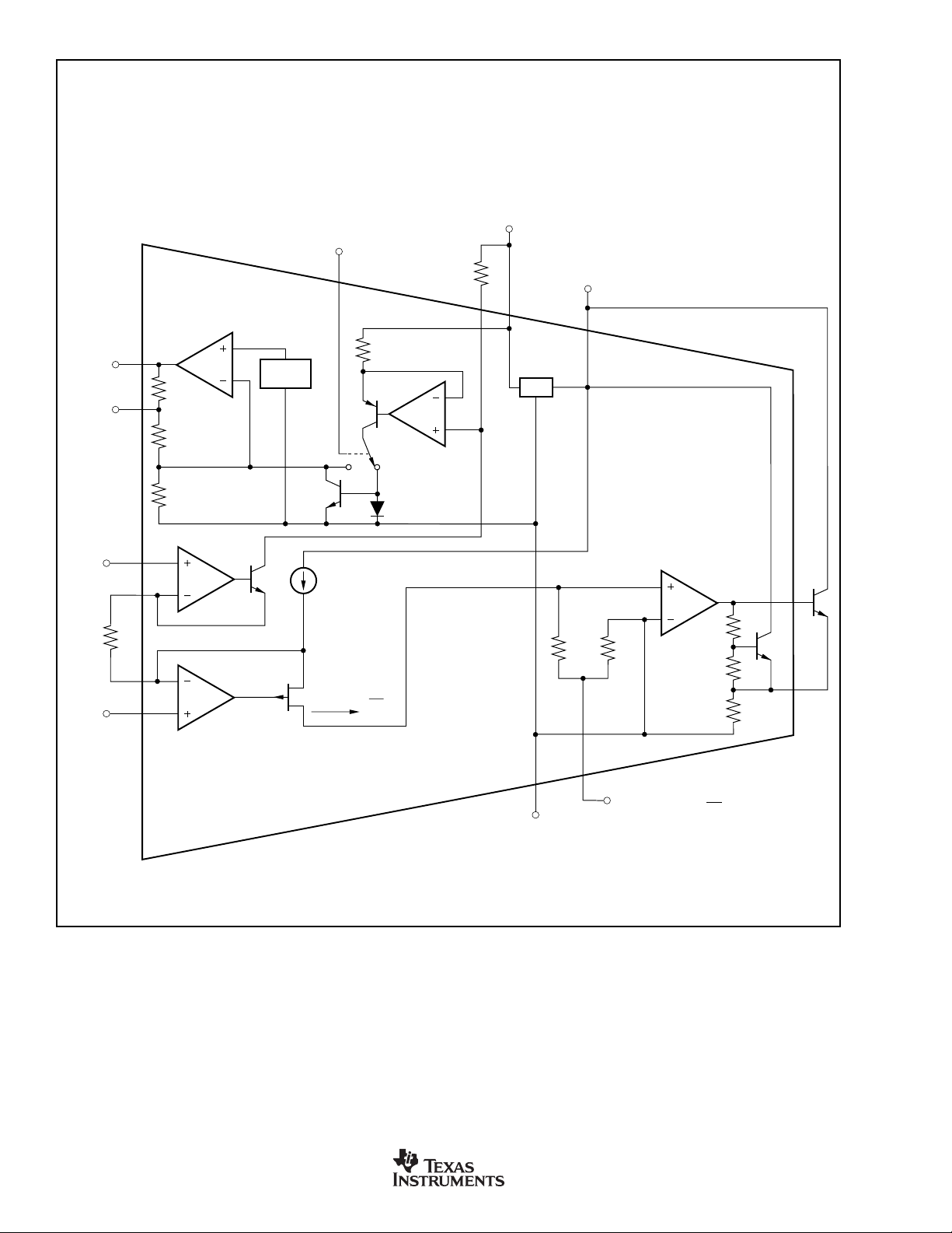
FUNCTIONAL DIAGRAM
Lin
Polarity
V
REG
12
R
LIN
11
1
V+
10
14
V
5
REF
REF
13
2.5
5
+
V
IN
V
4
REF
Amp
Bandgap
V
REF
100µA
Lin
Amp
Current
Direction
Switch
5.1V
B
9
R
G
975
3
V
2
–
V
IN
I = 100µA +
IN
R
G
25
Ω
Ω
E
8
6
I
RET
4
www.ti.com
7
= 4mA + V
I
O
• ( )
IN
40
R
G
XTR106
SBOS092A
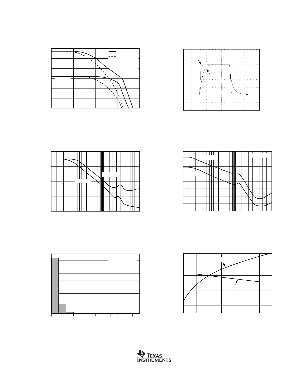
TYPICAL PERFORMANCE CURVES
At TA = +25°C, V+ = 24V, unless otherwise noted.
60
RG = 50Ω
50
40
30
RG = 1kΩ
C
C
OUT
C
OUT
connected
C
OUT
between V+ and I
20
TRANSCONDUCTANCE vs FREQUENCY
10
Transconductance (20 log mA/V)
= 250Ω
R
L
0
100 1k 10k 100k 1M
Frequency (Hz)
COMMON-MODE REJECTION vs FREQUENCY
110
100
90
80
70
RG = 1kΩ
RG = 50Ω
60
50
Common-Mode Rejection (dB)
40
30
10 1k100 10k 100k 1M
Frequency (Hz)
= 0.01µF
= 0.01µF
OUT
= 0.033µF
STEP RESPONSE
C
= 0.01µF
RG = 1kΩ
O
20mA
OUT
RG = 50Ω
4mA/div
4mA
50µs/div
POWER SUPPLY REJECTION vs FREQUENCY
160
140
RG = 50Ω
C
= 0
OUT
120
= 1kΩ
R
G
100
80
60
40
Power Supply Rejection (dB)
20
0
10 1k100 10k 100k 1M
Frequency (Hz)
90
80
70
60
50
40
30
Percent of Units (%)
20
10
0
XTR106
SBOS092A
INPUT OFFSET VOLTAGE DRIFT
PRODUCTION DISTRIBUTION
Typical production
distribution of
packaged units.
1.5
1.0
0.5
INPUT OFFSET VOLTAGE CHANGE
and V
vs V
REG
VOS vs I
CURRENTS
REF
REG
0
(µV)
–0.5
OS
∆ V
–1.0
VOS vs I
REF
–1.5
–2.0
–2.5
0
0.25
0.5
0.75
1.0
1.25
1.5
1.75
2.0
2.25
2.5
2.75
3.0
–1.0 –0.5 0 0.5 1.0 1.5 2.0 2.5
Current (mA)
Offset Voltage Drift (µV/°C)
www.ti.com
5
TYPICAL PERFORMANCE CURVES (CONT)
At TA = +25°C, V+ = 24V, unless otherwise noted.
2.5
UNDER-SCALE CURRENT vs TEMPERATURE
2.0
1.5
1.0
Under-Scale Current (mA)
0.5
V+ = 7.5V to 36V
0
–75 –50 –25 0 25 50 75 100
Temperature (°C)
OVER-SCALE CURRENT vs TEMPERATURE
30
With External Transistor
29
28
V+ = 36V
27
26
Over-Scale Current (mA)
25
V+ = 24V
V+ = 7.5V
24
–75 –50 –25 0 25 50 75 100
Temperature (°C)
125
125
4.0
UNDER-SCALE CURRENT vs I
REF
3.5
T
3.0
= –55°C
A
2.5
2.0
TA = +25°C
1.5
1.0
Under-Scale Current (mA)
TA = +125°C
0.5
0
0 0.5 1.0 1.5 2.0 2.5
+ I
REG
(mA)
I
REF
ZERO OUTPUT ERROR
3.0
vs V
REF
and V
CURRENTS
REG
2.5
2.0
I
ZERO
Error vs I
1.5
1.0
0.5
0
Zero Output Error (µA)
I
ZERO
Error vs I
–0.5
–1.0
–1 –0.5 0 0.5 1.0 1.5 2.0
Current (mA)
+ I
REG
REG
REF
2.5
ZERO OUTPUT CURRENT ERROR
4
2
0
–2
–4
–6
–8
Zero Output Current Error (µA)
–10
–12
–75 –50 –25 0 25 50 75 100
6
vs TEMPERATURE
Temperature (°C)
125
www.ti.com
70
60
50
40
30
20
Percent of Units (%)
10
0
0
0.1
0.05
0.15
ZERO OUTPUT DRIFT
PRODUCTION DISTRIBUTION
Typical production
distribution of
packaged units.
0.2
0.3
0.4
0.5
0.25
0.35
0.45
0.55
0.6
Zero Output Drift (µA/°C)
0.65
0.7
0.8
0.85
0.9
0.75
XTR106
SBOS092A
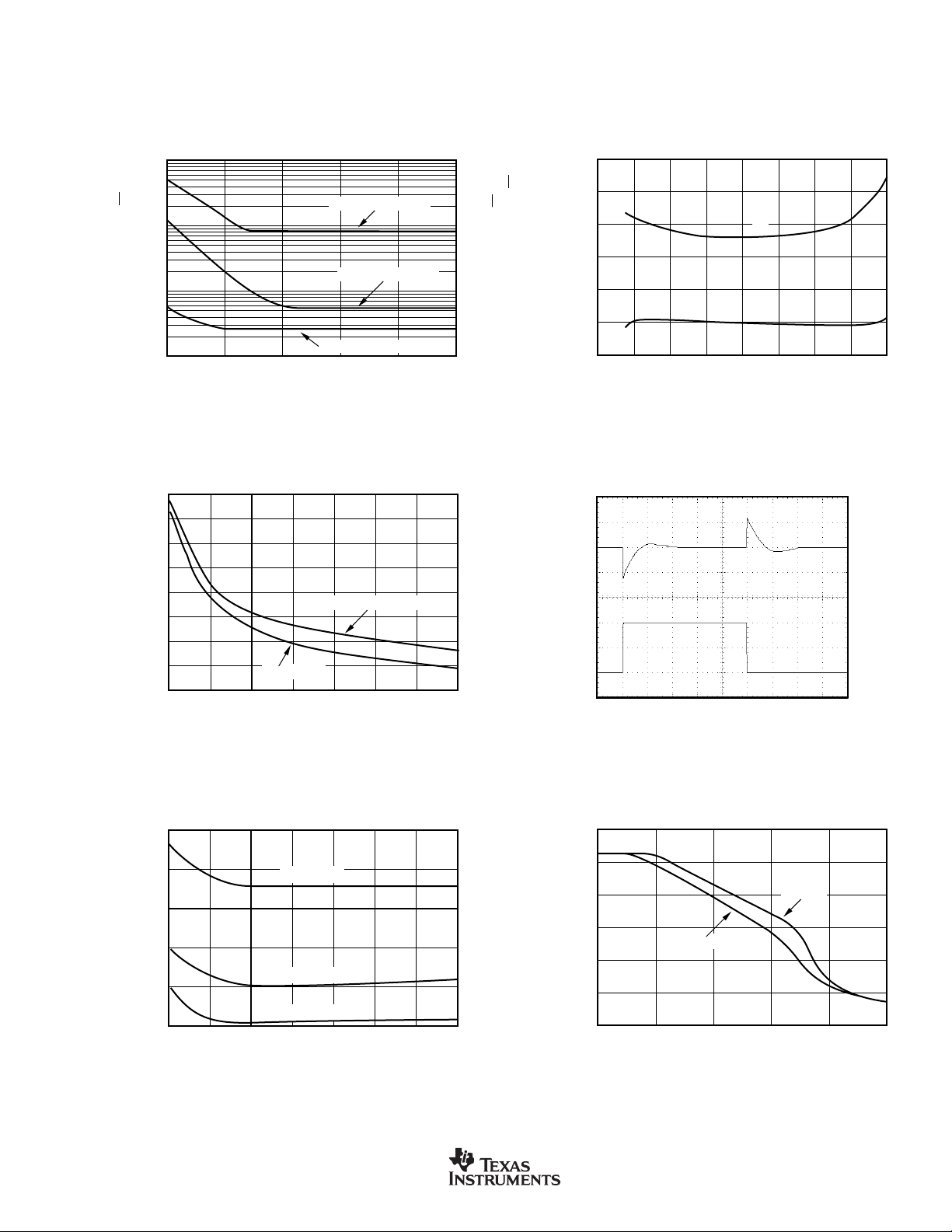
TYPICAL PERFORMANCE CURVES (CONT)
10 100 1k 10k 100k 1M
Frequency (Hz)
REFERENCE AC LINE REJECTION vs FREQUENCY
120
100
80
60
40
20
0
Line Rejection (dB)
V
REF
2.5
V
REF
5
At TA = +25°C, V+ = 24V, unless otherwise noted.
INPUT VOLTAGE, INPUT CURRENT, and ZERO
OUTPUT CURRENT NOISE DENSITY vs FREQUENCY
10k
Zero Output Noise
1k
Input Current Noise
100
Input Voltage Noise (nV/√Hz)
10
Input Voltage Noise
1 10 100 1k 10k
Frequency (Hz)
V
5.6
OUTPUT VOLTAGE vs V
REG
OUTPUT CURRENT
REG
5.5
5.4
5.3
5.2
5.1
Output Current (V)
REG
5.0
V
4.9
TA = +125°C
TA = +25°C, –55°C
4.8
–1.0 –0.5 0 0.5 1.0 1.5 2.0 2.5
Output Current (mA)
V
REG
100k
10k
1k
100
10
Input Current Noise (fA/√Hz)
Zero Output Current Noise (pA/√Hz)
INPUT BIAS and OFFSET CURRENT
vs TEMPERATURE
10
8
6
I
B
4
2
I
0
OS
Input Bias and Offset Current (nA)
–2
–75 –50 –25 0 25 50 75 100 125
Temperature (°C)
REFERENCE TRANSIENT RESPONSE
= 5V
V
REF
50mV/div
500µA/div
10µs/div
Output
Reference
1mA
0
5 vs V
V
REF
5.008
5.004
5.000
5 (V)
REF
V
4.996
4.992
4.988
–1.0 –0.5 0 0.5 1.0 1.5 2.0 2.5
V
REG
XTR106
SBOS092A
OUTPUT CURRENT
REG
T
= +25°C
A
T
= +125°C
A
T
= –55°C
A
Current (mA)
www.ti.com
7

TYPICAL PERFORMANCE CURVES (CONT)
At TA = +25°C, V+ = 24V, unless otherwise noted.
40
35
30
25
20
15
Percent of Units (%)
10
5
0
02468
REFERENCE VOLTAGE DRIFT
PRODUCTION DISTRIBUTION
Typical production
distribution of
packaged units.
101214161820222426283032343638
Reference Voltage Drift (ppm/°C)
REFERENCE VOLTAGE DEVIATION
0.1
0
–0.1
–0.2
–0.3
–0.4
Reference Voltage Deviation (%)
–0.5
40
–75 –50 –25 0 25 50 75 100 125
vs TEMPERATURE
V
= 2.5V
REF
Temperature (°C)
V
= 5V
REF
8
www.ti.com
XTR106
SBOS092A

APPLICATIONS INFORMATION
Figure 1 shows the basic connection diagram for the XTR106.
The loop power supply, VPS, provides power for all circuitry.
Output loop current is measured as a voltage across the series
load resistor, RL. A 0.01µF to 0.03µF supply bypass capacitor
connected between V+ and IO is recommended. For applications where fault and/or overload conditions might saturate
the inputs, a 0.03µF capacitor is recommended.
A 2.5V or 5V reference is available to excite a bridge sensor.
For 5V excitation, pin 14 (V
bridge as shown in Figure 1. For 2.5V excitation, connect
pin 13 (V
2.5) to pin 14 as shown in Figure 3b. The output
REF
terminals of the bridge are connected to the instrumentation
amplifier inputs, VIN and VIN. A 0.01µF capacitor is shown
connected between the inputs and is recommended for high
+–
impedance bridges (> 10kΩ). The resistor RG sets the gain
of the instrumentation amplifier as required by the full-scale
bridge voltage, VFS.
Lin Polarity and R
provide second-order linearization
LIN
correction to the bridge, achieving up to a 20:1 improvement
in linearity. Connections to Lin Polarity (pin 12) determine
the polarity of nonlinearity correction and should be connected either to I
nected to V
R
is chosen according to the equation in Figure 1 and is
LIN
REG
dependent on K
or V
RET
even if linearity correction is not desired.
(linearization constant) and the bridge’s
LIN
nonlinearity relative to VFS (see “Linearization” section).
5) should be connected to the
REF
. Lin Polarity should be con-
REG
The transfer function for the complete current transmitter is:
IO = 4mA + VIN • (40/RG)(1)
VIN in Volts, RG in Ohms
where V
is the differential input voltage. As evident from
IN
the transfer function, if no RG is used (RG = ∞), the gain is
zero and the output is simply the XTR106’s zero current.
A negative input voltage, V
, will cause the output current
IN
to be less than 4mA. Increasingly negative VIN will cause the
output current to limit at approximately 1.6mA. If current is
being sourced from the reference and/or V
, the current
REG
limit value may increase. Refer to the Typical Performance
Curves, “Under-Scale Current vs I
REF
+ I
REG
” and “Under-
Scale Current vs Temperature.”
Increasingly positive input voltage (greater than the full-
scale input, VFS) will produce increasing output current
according to the transfer function, up to the output current
limit of approximately 28mA. Refer to the Typical Performance Curve, “Over-Scale Current vs Temperature.”
The I
references and V
is the reference point for V
references. The I
pin is the return path for all current from the
RET
. I
REG
RET
also serves as a local ground and
RET
and the on-board voltage
REG
pin allows any current used in external
circuitry to be sensed by the XTR106 and to be included in
the output current without causing error. The input voltage
range of the XTR106 is referred to this pin.
5V
(5)
R
(5)
R
2
1
Bridge
Sensor
NOTES:
(1) Connect Lin Polarity (pin 12) to I
bridge nonlinearity or connect to V
nonlinearity. The R
V
if linearity correction is not desired. Refer to “Linearization”
REG
section and Figure 3.
(2) Recommended for bridge impedances > 10kΩ
( 3)
= K
R
LIN
R
+ –
B
pin and Lin Polarity pin must be connected to
LIN
4B
•
LIN
1 – 2B
For 2.5V excitation, connect
pin 13 to pin 14
C
IN
(2)
0.01µF
(pin 6) to correct for positive
RET
(pin 1) for negative bridge
REG
in Ω)
(K
LIN
V
REG
V
5
REF
V
2.5
REF
14
13
XTR106
6
11
R
LIN
(1)
Lin
Polarity
12
or
V
5
+
V
IN
4
R
G
(4)
R
G
3
R
G
–
V
2
IN
I
RET
(3)
R
LIN
1
REG
V
REG
(4)
R
(5) R
accuracy of the bridge. See “Bridge Balance” text.
7.5V to 36V
10
V+
9
B
Q
1
E
8
I
O
7
I = 4mA + V
O
(1)
= (VFS/400µA) •
G
where K
and R2 form bridge trim circuit to compensate for the initial
1
IN
= 9.905kΩ for 2.5V reference
LIN
= 6.645kΩ for 5V reference
K
LIN
B is the bridge nonlinearity relative to V
VFS is the full-scale input voltage
Possible choices for Q
C
OUT
0.01µF
40
• ( )
R
G
1 + 2B
1 – 2B
TYPE
2N4922
TIP29C
TIP31C
(V
FS
in V)
PACKAGE
4-20 mA
R
L
(see text).
1
TO-225
TO-220
TO-220
I
O
FS
V
O
+
V
PS
–
FIGURE 1. Basic Bridge Measurement Circuit with Linearization.
XTR106
SBOS092A
www.ti.com
9

EXTERNAL TRANSISTOR
External pass transistor, Q
, conducts the majority of the
1
signal-dependent 4-20mA loop current. Using an external
transistor isolates the majority of the power dissipation from
the precision input and reference circuitry of the XTR106,
maintaining excellent accuracy.
Since the external transistor is inside a feedback loop its
characteristics are not critical. Requirements are: V
CEO
= 45V
min, β = 40 min and PD = 800mW. Power dissipation requirements may be lower if the loop power supply voltage is less
than 36V. Some possible choices for Q1 are listed in Figure 1.
The XTR106 can be operated without an external pass
transistor. Accuracy, however, will be somewhat degraded
due to the internal power dissipation. Operation without Q
is not recommended for extended temperature ranges. A
resistor (R = 3.3kΩ) connected between the I
pin and the
RET
E (emitter) pin may be needed for operation below 0°C
without Q1 to guarantee the full 20mA full-scale output,
especially with V+ near 7.5V.
10
V+
8
E
I
RET
XTR106
6
= 3.3kΩ
R
Q
I
O
7
0.01µF
For operation without external
transistor, connect a 3.3kΩ
resistor between pin 6 and
pin 8. See text for discussion
of performance.
FIGURE 2. Operation without External Transistor.
LOOP POWER SUPPLY
The voltage applied to the XTR106, V+, is measured with
respect to the IO connection, pin 7. V+ can range from 7.5V
to 36V. The loop supply voltage, VPS, will differ from the
voltage applied to the XTR106 according to the voltage drop
on the current sensing resistor, RL (plus any other voltage
drop in the line).
If a low loop supply voltage is used, RL (including the loop
wiring resistance) must be made a relatively low value to
assure that V+ remains 7.5V or greater for the maximum
loop current of 20mA:
RLmax =
(V+)–7.5V
20mA
–R
WIRING
(2)
It is recommended to design for V+ equal or greater than
7.5V with loop currents up to 30mA to allow for out-ofrange input conditions. V+ must be at least 8V if 5V sensor
excitation is used and if correcting for bridge nonlinearity
greater than +3%.
The low operating voltage (7.5V) of the XTR106 allows
operation directly from personal computer power supplies
(12V ±5%). When used with the RCV420 Current Loop
Receiver (Figure 8), load resistor voltage drop is limited to 3V.
BRIDGE BALANCE
Figure 1 shows a bridge trim circuit (R1, R2). This adjustment can be used to compensate for the initial accuracy of
the bridge and/or to trim the offset voltage of the XTR106.
The values of R1 and R2 depend on the impedance of the
bridge, and the trim range required. This trim circuit places
an additional load on the V
load on V
does not affect zero output. See the Typical
REF
output. Be sure the additional
REF
Performance Curve, “Under-Scale Current vs I
1
The effective load of the trim circuit is nearly equal to R2.
An approximate value for R1 can be calculated:
5V • R
R1≈
4 • V
B
TRIM
where, RB is the resistance of the bridge.
V
is the desired ±voltage trim range (in V).
TRIM
Make R2 equal or lower in value to R1.
LINEARIZATION
Many bridge sensors are inherently nonlinear. With the
addition of one external resistor, it is possible to compensate
for parabolic nonlinearity resulting in up to 20:1 improvement over an uncompensated bridge output.
Linearity correction is accomplished by varying the bridge
excitation voltage. Signal-dependent variation of the bridge
excitation voltage adds a second-order term to the overall
transfer function (including the bridge). This can be tailored
to correct for bridge sensor nonlinearity.
Either positive or negative bridge non-linearity errors can be
compensated by proper connection of the Lin Polarity pin.
To correct for positive bridge nonlinearity (upward bowing),
Lin Polarity (pin 12) should be connected to I
shown in Figure 3a. This causes V
to increase with bridge
REF
output which compensates for a positive bow in the bridge
response. To correct negative nonlinearity (downward bowing), connect Lin Polarity to V
3b. This causes V
to decrease with bridge output. The Lin
REF
(pin 1) as shown in Figure
REG
Polarity pin is a high impedance node.
If no linearity correction is desired, both the R
Polarity pins should be connected to V
(Figure 3c). This
REG
results in a constant reference voltage independent of input
signal. R
or Lin Polarity pins should not be left open
LIN
or connected to another potential.
R
is the external linearization resistor and is connected
LIN
between pin 11 and pin 1 (V
3b. To determine the value of R
) as shown in Figures 3a and
REG
, the nonlinearity of the
LIN
bridge sensor with constant excitation voltage must be
known. The XTR106’s linearity circuitry can only compensate for the parabolic-shaped portions of a sensor’s
nonlinearity. Optimum correction occurs when maximum
deviation from linear output occurs at mid-scale (see Figure
4). Sensors with nonlinearity curves similar to that shown in
+ I
REF
(pin 6) as
RET
and Lin
LIN
REG
.”
(3)
10
www.ti.com
XTR106
SBOS092A

Figure 4, but not peaking exactly at mid-scale can be
substantially improved. A sensor with a “S-shaped”
nonlinearity curve (equal positive and negative nonlinearity)
cannot be improved with the XTR106’s correction circuitry.
The value of R
in Figure 3. R
K
, which differs for the 2.5V reference and 5V reference.
LIN
is chosen according to Equation 4 shown
LIN
is dependent on a linearization factor,
LIN
The sensor’s nonlinearity term, B (relative to full scale), is
positive or negative depending on the direction of the bow.
V
REG
V
5
REF
5V
R
R
2
1
+ –
3a. Connection for Positive Bridge Nonlinearity, V
V
2.5
REF
2.5V
R
R
2
1
+ –
3b. Connection for Negative Bridge Nonlinearity, V
V
5
REF
5V
R
R
2
1
+ –
3c. Connection if no linearity correction is desired, V
V
2.5
REF
14
+
–
5
+
–
+
–
REF
6
14
6
REF
V
14
6
REF
13
XTR106
I
RET
= 5V
13
XTR106
= 2.5V
2.5
REF
13
XTR106
= 5V
5
4
R
G
3
2
V
REF
5
4
R
G
3
2
I
RET
5
4
R
G
3
2
I
RET
V
V
1
12
REG
12
REG
12
Lin
Polarity
1
Lin
Polarity
1
Lin
Polarity
R
LIN
11
R
LIN
11
R
LIN
11
A maximum ±5% non-linearity can be corrected when the
5V reference is used. Sensor nonlinearity of +5%/–2.5% can
be corrected with 2.5V excitation. The trim circuit shown in
Figure 3d can be used for bridges with unknown bridge
nonlinearity polarity.
Gain is affected by the varying excitation voltage used to
correct bridge nonlinearity. The corrected value of the gain
resistor is calculated from Equation 5 given in Figure 3.
XTR106
V
Lin
Polarity
I
RET
6
R
X
100kΩ
Open RX for negative bridge nonlinearity
Open R
for positive bridge nonlinearity
Y
3d. On-Board Resistor Circuit for Unknown Bridge Nonlinearity Polarity
EQUATIONS
Linearization Resistor:
R
= K
LIN
4B
•
LIN
1– 2B
Gain-Set Resistor:
V
1+ 2B
FS
RG=
400µA
•
1– 2B
Adjusted Excitation Voltage at Full-Scale Output:
V
where, K
REF(Adj)
= V
REF(Initial)
is the linearization factor (in Ω)
LIN
K
= 9905Ω for the 2.5V reference
LIN
K
= 6645Ω for the 5V reference
LIN
B is the sensor nonlinearity relative to V
(for –2.5% nonlinearity, B = –0.025)
V
is the full-scale bridge output without
FS
linearization (in V)
•
1+ 2B
1– 2B
Example:
Calculate R
2.5% downward bow nonlinearity relative to V
if the input common-mode range is valid.
V
REF
For a 2.5% downward bow, B = –0.025
(Lin Polarity pin connected to V
For V
R
LIN
RG=
VCM=
which falls within the 1.1V to 3.5V input common-mode range.
and the resulting RG for a bridge sensor with
LIN
= 2.5V and VFS = 50mV
= 2.5V, K
REF
(9905Ω)(4)(–0.025)
=
1– (2)(–0.025)
0.05V
400µA
V
REF(Adj)
2
= 9905Ω
LIN
1+ (2)( –0.025)
•
1– (2)(–0.025)
1
=
• 2. 5V •
2
REG
1
12
R
Y
15kΩ
(in Ω)
(in Ω)
(in V)
)
REG
= 943Ω
= 113Ω
1+ (2)( –0.025)
1– (2)(–0.025)
FS
and determine
FS
= 1.1 3V
(4)
(5)
(6)
FIGURE 3. Connections and Equations to Correct Positive and Negative Bridge Nonlinearity.
XTR106
SBOS092A
www.ti.com
11

When using linearity correction, care should be taken to
insure that the sensor’s output common-mode voltage remains within the XTR106’s allowable input range of 1.1V to
3.5V. Equation 6 in Figure 3 can be used to calculate the
XTR106’s new excitation voltage. The common-mode voltage of the bridge output is simply half this value if no
common-mode resistor is used (refer to the example in
Figure 3). Exceeding the common-mode range may yield
unpredicatable results.
For high precision applications (errors < 1%), a two-step
calibration process can be employed. First, the nonlinearity
of the sensor bridge is measured with the initial gain resistor
and R
the resulting sensor nonlinearity, B, values for RG and R
LIN
= 0 (R
pin connected directly to V
LIN
REG
). Using
LIN
are calculated using Equations 4 and 5 from Figure 3. A
second calibration measurement is then taken to adjust RG to
account for the offsets and mismatches in the linearization.
UNDER-SCALE CURRENT
The total current being drawn from the V
REF
and V
REG
voltage sources, as well as temperature, affect the XTR106’s
under-scale current value (see the Typical Performance
Curve, “Under-Scale Current vs I
REF
+ I
). This should be
REG
considered when choosing the bridge resistance and excitation voltage, especially for transducers operating over a
wide temperature range (see the Typical Performance Curve,
“Under-Scale Current vs Temperature”).
LOW IMPEDANCE BRIDGES
The XTR106’s two available excitation voltages (2.5V and
5V) allow the use of a wide variety of bridge values. Bridge
impedances as low as 1kΩ can be used without any additional circuitry. Lower impedance bridges can be used with
the XTR106 by adding a series resistance to limit excitation
current to ≤ 2.5mA (Figure 5). Resistance should be added
BRIDGE TRANSDUCER TRANSFER FUNCTION
10
9
8
7
6
5
4
3
Bridge Output (mV)
2
1
0
0
WITH PARABOLIC NONLINEARITY
Positive Nonlinearity
B = +0.025
B = –0.019
Negative Nonlinearity
Linear Response
0.1 0.2 0.3 0.4 0.5 0.6 0.7 0.8 0.9 1
Normalized Stimulus
FIGURE 4. Parabolic Nonlinearity.
700µA at 5V
I
≈ 1.6mA
1/2
OPA2277
412Ω
1/2
OPA2277
amplifier
REG
10kΩ
10kΩ
3.4kΩ
5V
350Ω
3.4kΩ
Bridge excitation
voltage = 0.245V
Approx. x50
FIGURE 5. 350Ω Bridge with x50 Preamplifier.
1kΩ
V
R
125Ω
3
2
1
0
–1
–2
Nonlinearity (% of Full Scale)
–3
0
0.1 0.2 0.3 0.4 0.5 0.6 0.7 0.8 0.9 1
5
REF
V
2.5
V
REF
REG
14
13
5
+
V
IN
4
R
G
G
XTR106
3
R
G
–
V
IN
2
I
RET
1
Polarity
6
Lin
R
11
V+
I
12
NONLINEARITY vs STIMULUS
Positive Nonlinearity
B = +0.025
Negative Nonlinearity
Normalized Stimulus
I
= 0.7mA + 1.6mA ≤ 2.5mA
TOTAL
LIN
10
9
B
E
8
O
7
Shown connected to correct positive
bridge nonlinearity. For negative bridge
nonlinearity, see Figure 3b.
1N4148
0.01µF
IO = 4-20mA
B = –0.019
12
www.ti.com
XTR106
SBOS092A

to the upper and lower sides of the bridge to keep the bridge
output within the 1.1V to 3.5V common-mode input range.
Bridge output is reduced so a preamplifier as shown may be
needed to reduce offset voltage and drift.
OTHER SENSOR TYPES
The XTR106 can be used with a wide variety of inputs. Its
high input impedance instrumentation amplifier is versatile
and can be configured for differential input voltages from
millivolts to a maximum of 2.4V full scale. The linear range
of the inputs is from 1.1V to 3.5V, referenced to the I
RET
terminal, pin 6. The linearization feature of the XTR106 can
ERROR ANALYSIS
Table I shows how to calculate the effect various error
sources have on circuit accuracy. A sample error calculation
for a typical bridge sensor measurement circuit is shown
(5kΩ bridge, V
= 5V, VFS = 50mV) is provided. The
REF
results reveal the XTR106’s excellent accuracy, in this case
1.2% unadjusted. Adjusting gain and offset errors improves
circuit accuracy to 0.33%. Note that these are worst-case
errors; guaranteed maximum values were used in the calculations and all errors were assumed to be positive (additive).
The XTR106 achieves performance which is difficult to
obtain with discrete circuitry and requires less board space.
be used with any sensor whose output is ratiometric with an
excitation voltage.
SAMPLE ERROR CALCULATION
Bridge Impedance (RB)5kΩ Full Scale Input (VFS) 50mV
Ambient Temperature Range (∆T
Supply Voltage Change (∆V+) 5V Common-Mode Voltage Change (∆CM) 25mV (= V
ERROR SOURCE ERROR EQUATION ERROR CALCULATION UNADJ ADJUST
INPUT
Input Offset Voltage V
vs Common-Mode CMRR • ∆CM/VFS • 10
vs Power Supply (V
Input Bias Current CMRR • I
Input Offset Current IOS • RB/VFS • 10
EXCITATION
Voltage Reference Accuracy V
vs Supply (V
GAIN
Span Span Error (%)/100% • 10
Nonlinearity Nonlinearity (%)/100% • 10
OUTPUT
Zero Output | I
vs Supply (I
DRIFT (∆T
= 20°C)
A
Input Offset Voltage Drift • ∆T
Input Offset Current (typical) Drift • ∆TA• RB/(VFS) • 10
Voltage Refrence Accuracy 35ppm/°C • 20°C 700 700
Span 225ppm/°C • 20°C 500 500
Zero Output Drift • ∆T
NOISE (0.1Hz to 10Hz, typ)
Input Offset Voltage V
Zero Output I
Thermal R
Noise
B
Input Current Noise (i
NOTE (1): All errors are min/max and referred to input, unless otherwise stated.
)20°C Excitation Voltage (V
A
SAMPLE
6
• 10
OS/VFS
vs V+) • (∆V+)/VFS • 10
OS
• (RB/2)/VFS • 10
B
Accuracy (%)/100% • 10
REF
vs V+) • (∆V+) • (VFS/V
REF
– 4mA | /16000 µA • 10
ZERO
vs V+) • (∆V+)/16000µA • 10
ZERO
/(VFS) • 10
A
/16000µA • 10
A
(p-p)/VFS • 10
n
Noise/ 16000µA • 10
ZERO
6
6
6
6
6
) 20ppm/V • 5V (50mV/5V) 1 1
REF
6
6
6
6
6
6
6
6
6
[√2 • √ (RB/2)/1kΩ • 4nV / √Hz • √ 10Hz]/ VFS • 10
• 40.8 • √2 • RB/2)/VFS •
n
6
10
)5V
REF
200µV/50mV • 10
50µV/V • 0.025V/50mV • 10
3µV/V • 5V/50mV • 10
50µV/V • 25nA • 2.5kΩ/50mV • 10
3nA • 5kΩ/50mV • 10
0.25%/100% • 10
0.2%/100% • 10
0.01%/100% • 10
25µA/16000µA • 10
0.2µA/V • 5V/16000µA • 10
1.5µV/°C • 20°C / (50mV) • 10
5pA/ °C • 20°C • 5kΩ/ (50mV) • 10
0.9µA/°C • 20°C/16000µA • 10
0.6µV/ 50mV • 10
6
[√2 • √ 2.5kΩ/1kΩ • 4nV/ √Hz • √ 10Hz ] / 50mV • 10
0.035µA/16000µA • 10
(200fA/√Hz • 40.8 • √2 • 2.5kΩ)/50mV• 10
/2)
FS
6
6
6
6
6
Total Input Error 2625 325
6
Total Excitation Error 2501 1
6
6
Total Gain Error 2100 100
6
6
Total Output Error 1626 63
6
6
6
Total Drift Error 2936 2936
6
6
6
6
Total Noise Error 15 15
TOTAL ERROR: 11803 3340
1.18% 0.33%
ERROR
(ppm of Full Scale)
2000 0
25 25
300 300
0.1 0
300 0
2500 0
2000 0
100 100
1563 0
62.5 62.5
600 600
10 10
1125 1125
12 12
2.2 2.2
0.6 0.6
0.6 0.6
TABLE I. Error Calculation.
XTR106
SBOS092A
www.ti.com
13

REVERSE-VOLTAGE PROTECTION
The XTR106’s low compliance rating (7.5V) permits the
use of various voltage protection methods without compromising operating range. Figure 6 shows a diode bridge
circuit which allows normal operation even when the voltage connection lines are reversed. The bridge causes a two
diode drop (approximately 1.4V) loss in loop supply voltage. This results in a compliance voltage of approximately
9V—satisfactory for most applications. A diode can be
inserted in series with the loop supply voltage and the V+
pin as shown in Figure 8 to protect against reverse output
connection lines with only a 0.7V loss in loop supply
voltage.
OVER-VOLTAGE SURGE PROTECTION
Remote connections to current transmitters can sometimes be
subjected to voltage surges. It is prudent to limit the maximum
surge voltage applied to the XTR106 to as low as practical.
Various zener diode and surge clamping diodes are specially
designed for this purpose. Select a clamp diode with as low a
voltage rating as possible for best protection. For example, a
36V protection diode will assure proper transmitter operation
at normal loop voltages, yet will provide an appropriate level
of protection against voltage surges. Characterization tests on
three production lots showed no damage to the XTR106 with
loop supply voltages up to 65V.
Most surge protection zener diodes have a diode characteristic in the forward direction that will conduct excessive
current, possibly damaging receiving-side circuitry if the
loop connections are reversed. If a surge protection diode is
used, a series diode or diode bridge should be used for
protection against reversed connections.
RADIO FREQUENCY INTERFERENCE
The long wire lengths of current loops invite radio frequency interference. RF can be rectified by the sensitive
input circuitry of the XTR106 causing errors. This generally
appears as an unstable output current that varies with the
position of loop supply or input wiring.
If the bridge sensor is remotely located, the interference may
enter at the input terminals. For integrated transmitter assemblies with short connection to the sensor, the interference more likely comes from the current loop connections.
Bypass capacitors on the input reduce or eliminate this input
interference. Connect these bypass capacitors to the I
RET
terminal as shown in Figure 6. Although the dc voltage at
the I
terminal is not equal to 0V (at the loop supply, VPS)
RET
this circuit point can be considered the transmitter’s “ground.”
The 0.01µF capacitor connected between V+ and IO may
help minimize output interference.
V
5
+ –
Bridge
Sensor
5V
REF
R
B
R
G
0.01µF0.01µF
V
2.5
REF
14
5
4
3
2
13
+
V
IN
R
G
XTR106
R
G
–
V
IN
I
RET
6
10
V+
9
B
E
8
I
O
7
NOTE: (1) Zener Diode 36V: 1N4753A or Motorola
P6KE39A. Use lower voltage zener diodes with loop
power supply voltages less than 30V for increased
protection. See “Over-Voltage Surge Protection.”
0.01µF
Q
1
FIGURE 6. Reverse Voltage Operation and Over-Voltage Surge Protection.
(1)
D
1
1N4148
Diodes
The diode bridge causes
a 1.4V loss in loop supply
voltage.
Maximum V
less than minimum
voltage rating of zener
diode.
R
L
must be
PS
V
PS
14
www.ti.com
XTR106
SBOS092A

Type K
Isothermal
Block
1N4148
6kΩ
50Ω
4.8kΩ
5.2kΩ
100Ω
1MΩ
V
5
REF
0.01µF
See ISO124 data sheet
if isolation is needed.
1MΩ
20kΩ
OPA277
(1)
R
1kΩ
V
2.5
REF
14
13
I
RET
11
R
LIN
XTR106
Lin
Polarity
1
V
REG
12
5
+
V
IN
4
R
G
G
3
R
G
–
V
2
IN
6
V
REG
7.5V to 36V
10
V+
9
Q
B
1
E
8
I
O
7
IO = 4mA + VIN • ( )
(pin 1)
C
OUT
0.01µF
40
R
G
4-20 mA
R
L
I
O
V
O
+
V
PS
–
2kΩ
NOTE: (1) For burn-out indication.
0.01µF
FIGURE 7. Thermocouple Low Offset, Low Drift Loop Measurement with Diode Cold-Junction Compensation.
V
2.5
Bridge
Sensor
2.5V
– +
R
B
REF
5
V
REF
14
+
V
5
IN
4
R
G
R
G
3
R
G
–
2
V
IN
I
RET
6
13
XTR106
Lin
Polarity
V
REG
R
LIN
1
11
10
1N4148
See ISO124 data sheet
if isolation is needed.
+12V
1µF
V+
9
B
8
E
I
O
0.01µF
7
12
IO = 4-20mA
3
2
16
10
11
RCV420
4
1µF
12
15
V
14
O
13
5
= 0V to 5V
NOTE: Lin Polarity shown connected to correct positive bridge
nonlinearity. See Figure 3b to correct negative bridge nonlinearity.
FIGURE 8. ±12V-Powered Transmitter/Receiver Loop.
XTR106
SBOS092A
www.ti.com
–12V
15

PACKAGE OPTION ADDENDUM
www.ti.com
22-Oct-2007
PACKAGING INFORMATION
Orderable Device Status
(1)
Package
Type
Package
Drawing
Pins Package
Qty
Eco Plan
XTR106P ACTIVE PDIP N 14 25 Green (RoHS &
no Sb/Br)
XTR106PA ACTIVE PDIP N 14 25 Green (RoHS &
no Sb/Br)
XTR106PAG4 ACTIVE PDIP N 14 25 Green (RoHS &
no Sb/Br)
XTR106PG4 ACTIVE PDIP N 14 25 Green(RoHS &
no Sb/Br)
XTR106U ACTIVE SOIC D 14 58 Green (RoHS &
no Sb/Br)
XTR106U/2K5 ACTIVE SOIC D 14 2500 Green (RoHS &
no Sb/Br)
XTR106U/2K5E4 ACTIVE SOIC D 14 2500 Green (RoHS &
no Sb/Br)
XTR106UA ACTIVE SOIC D 14 58 Green (RoHS &
no Sb/Br)
XTR106UA/2K5 ACTIVE SOIC D 14 2500 Green (RoHS &
no Sb/Br)
XTR106UA/2K5E4 ACTIVE SOIC D 14 2500 Green (RoHS &
no Sb/Br)
XTR106UAG4 ACTIVE SOIC D 14 58 Green (RoHS &
no Sb/Br)
XTR106UE4 ACTIVE SOIC D 14 58 Green (RoHS &
no Sb/Br)
(1)
The marketing status values are defined as follows:
ACTIVE: Product device recommended for new designs.
LIFEBUY: TI has announced that the device will be discontinued, and a lifetime-buy period is in effect.
NRND: Not recommended for new designs. Device is in production to support existing customers, but TI does not recommend using this part in
a new design.
PREVIEW: Device has been announced but is not in production. Samples may or may not be available.
OBSOLETE: TI has discontinued the production of the device.
(2)
Lead/Ball Finish MSL Peak Temp
CU NIPDAU N / A for Pkg Type
CU NIPDAU N / A for Pkg Type
CU NIPDAU N / A for Pkg Type
CU NIPDAU N / A for Pkg Type
CU NIPDAU Level-3-260C-168 HR
CU NIPDAU Level-3-260C-168 HR
CU NIPDAU Level-3-260C-168 HR
CU NIPDAU Level-3-260C-168 HR
CU NIPDAU Level-3-260C-168 HR
CU NIPDAU Level-3-260C-168 HR
CU NIPDAU Level-3-260C-168 HR
CU NIPDAU Level-3-260C-168 HR
(3)
(2)
Eco Plan - The planned eco-friendly classification: Pb-Free (RoHS), Pb-Free (RoHS Exempt), or Green (RoHS & no Sb/Br) - please check
http://www.ti.com/productcontent for the latest availability information and additional product content details.
TBD: The Pb-Free/Green conversion plan has not been defined.
Pb-Free (RoHS): TI's terms "Lead-Free" or "Pb-Free" mean semiconductor products that are compatible with the current RoHS requirements
for all 6 substances, including the requirement that lead not exceed 0.1% by weight in homogeneous materials. Where designed to be soldered
at high temperatures, TI Pb-Free products are suitable for use in specified lead-free processes.
Pb-Free (RoHS Exempt): This component has a RoHS exemption for either 1) lead-based flip-chip solder bumps used between the die and
package, or 2) lead-based die adhesive used between the die and leadframe. The component is otherwise considered Pb-Free (RoHS
compatible) as defined above.
Green (RoHS & no Sb/Br): TI defines "Green" to mean Pb-Free (RoHS compatible), and free of Bromine (Br) and Antimony (Sb) based flame
retardants (Br or Sb do not exceed 0.1% by weight in homogeneous material)
(3)
MSL, Peak Temp. -- The Moisture Sensitivity Level rating according to the JEDEC industry standard classifications, and peak solder
temperature.
Important Information and Disclaimer:The information provided on this page represents TI's knowledge and belief as of the date that it is
provided. TI bases its knowledge and belief on information provided by third parties, and makes no representation or warranty as to the
accuracy of such information. Efforts are underway to better integrate information from third parties. TI has taken and continues to take
reasonable steps to provide representative and accurate information but may not have conducted destructive testing or chemical analysis on
incoming materials and chemicals. TI and TI suppliers consider certain information to be proprietary, and thus CAS numbers and other limited
information may not be available for release.
Addendum-Page 1

PACKAGE OPTION ADDENDUM
www.ti.com
In no event shall TI's liability arising out of such information exceed the total purchase price of the TI part(s) at issue in this document sold by TI
to Customer on an annual basis.
22-Oct-2007
Addendum-Page 2

PACKAGE MATERIALS INFORMATION
www.ti.com
TAPE AND REEL INFORMATION
11-Mar-2008
*All dimensions are nominal
Device Package
XTR106U/2K5 SOIC D 14 2500 330.0 16.4 6.5 9.0 2.1 8.0 16.0 Q1
XTR106UA/2K5 SOIC D 14 2500 330.0 16.4 6.5 9.0 2.1 8.0 16.0 Q1
Type
Package
Drawing
Pins SPQ Reel
Diameter
(mm)
Reel
Width
W1 (mm)
A0 (mm) B0 (mm) K0 (mm) P1
(mm)W(mm)
Pin1
Quadrant
Pack Materials-Page 1

PACKAGE MATERIALS INFORMATION
www.ti.com
11-Mar-2008
*All dimensions are nominal
Device Package Type Package Drawing Pins SPQ Length (mm) Width (mm) Height (mm)
XTR106U/2K5 SOIC D 14 2500 346.0 346.0 33.0
XTR106UA/2K5 SOIC D 14 2500 346.0 346.0 33.0
Pack Materials-Page 2


IMPORTANT NOTICE
Texas Instruments Incorporated and its subsidiaries (TI) reserve the right to make corrections, modifications, enhancements, improvements,
and other changes to its products and services at any time and to discontinue any product or service without notice. Customers should
obtain the latest relevant information before placing orders and should verify that such information is current and complete. All products are
sold subject to TI’s terms and conditions of sale supplied at the time of order acknowledgment.
TI warrants performance of its hardware products to the specifications applicable at the time of sale in accordance with TI’s standard
warranty. Testing and other quality control techniques are used to the extent TI deems necessary to support this warranty. Except where
mandated by government requirements, testing of all parameters of each product is not necessarily performed.
TI assumes no liability for applications assistance or customer product design. Customers are responsible for their products and
applications using TI components. To minimize the risks associated with customer products and applications, customers should provide
adequate design and operating safeguards.
TI does not warrant or represent that any license, either express or implied, is granted under any TI patent right, copyright, mask work right,
or other TI intellectual property right relating to any combination, machine, or process in which TI products or services are used. Information
published by TI regarding third-party products or services does not constitute a license from TI to use such products or services or a
warranty or endorsement thereof. Use of such information may require a license from a third party under the patents or other intellectual
property of the third party, or a license from TI under the patents or other intellectual property of TI.
Reproduction of TI information in TI data books or data sheets is permissible only if reproduction is without alteration and is accompanied
by all associated warranties, conditions, limitations, and notices. Reproduction of this information with alteration is an unfair and deceptive
business practice. TI is not responsible or liable for such altered documentation. Information of third parties may be subject to additional
restrictions.
Resale of TI products or services with statements different from or beyond the parameters stated by TI for that product or service voids all
express and any implied warranties for the associated TI product or service and is an unfair and deceptive business practice. TI is not
responsible or liable for any such statements.
TI products are not authorized for use in safety-critical applications (such as life support) where a failure of the TI product would reasonably
be expected to cause severe personal injury or death, unless officers of the parties have executed an agreement specifically governing
such use. Buyers represent that they have all necessary expertise in the safety and regulatory ramifications of their applications, and
acknowledge and agree that they are solely responsible for all legal, regulatory and safety-related requirements concerning their products
and any use of TI products in such safety-critical applications, notwithstanding any applications-related information or support that may be
provided by TI. Further, Buyers must fully indemnify TI and its representatives against any damages arising out of the use of TI products in
such safety-critical applications.
TI products are neither designed nor intended for use in military/aerospace applications or environments unless the TI products are
specifically designated by TI as military-grade or "enhanced plastic." Only products designated by TI as military-grade meet military
specifications. Buyers acknowledge and agree that any such use of TI products which TI has not designated as military-grade is solely at
the Buyer's risk, and that they are solely responsible for compliance with all legal and regulatory requirements in connection with such use.
TI products are neither designed nor intended for use in automotive applications or environments unless the specific TI products are
designated by TI as compliant with ISO/TS 16949 requirements. Buyers acknowledge and agree that, if they use any non-designated
products in automotive applications, TI will not be responsible for any failure to meet such requirements.
Following are URLs where you can obtain information on other Texas Instruments products and application solutions:
Products Applications
Amplifiers amplifier.ti.com Audio www.ti.com/audio
Data Converters dataconverter.ti.com Automotive www.ti.com/automotive
DSP dsp.ti.com Broadband www.ti.com/broadband
Clocks and Timers www.ti.com/clocks Digital Control www.ti.com/digitalcontrol
Interface interface.ti.com Medical www.ti.com/medical
Logic logic.ti.com Military www.ti.com/military
Power Mgmt power.ti.com Optical Networking www.ti.com/opticalnetwork
Microcontrollers microcontroller.ti.com Security www.ti.com/security
RFID www.ti-rfid.com Telephony www.ti.com/telephony
RF/IF and ZigBee® Solutions www.ti.com/lprf Video & Imaging www.ti.com/video
Mailing Address: Texas Instruments, Post Office Box 655303, Dallas, Texas 75265
Copyright © 2008, Texas Instruments Incorporated
Wireless www.ti.com/wireless
 Loading...