

Page 1

XIO3130
Data Manual
PRODUCTION DATA information is current as of publication date.
Products conform to specifications per the terms of the Texas
Instruments standard warranty. Production processing does not
necessarily include testing of all parameters.
Literature Number: SLLS693E
May 2007 – Revised April 2009
Page 2

XIO3130
SLLS693E – MAY 2007 – REVISED APRIL 2009
www.ti.com
Contents
1 Features ............................................................................................................................ 11
2 Introduction ....................................................................................................................... 12
2.1 Description .................................................................................................................. 12
2.2 Related Documents ........................................................................................................ 12
2.3 Document Conventions .................................................................................................... 13
2.4 Ordering Information ...................................................................................................... 13
2.5 Terminal Assignments ..................................................................................................... 14
2.6 Terminal Descriptions ...................................................................................................... 17
3 Description ........................................................................................................................ 22
3.1 Power-Up/Power-Down Sequencing ..................................................................................... 22
3.1.1 Power-Up Sequence ............................................................................................ 22
3.1.2 Power-Down Sequence ......................................................................................... 23
3.2 Express Interface ........................................................................................................... 23
3.2.1 External Reference Clock ...................................................................................... 23
3.2.2 Clock Generator ................................................................................................. 23
3.2.3 Beacon ............................................................................................................ 24
3.2.4 WAKE ............................................................................................................ 24
3.2.5 Initial Flow Control Credits ..................................................................................... 24
3.2.6 PCI Express Message Transactions .......................................................................... 24
3.3 GPIO Terminals ............................................................................................................ 25
3.4 Serial EEPROM ............................................................................................................ 25
3.4.1 Serial Bus Interface Implementation .......................................................................... 26
3.4.2 Serial Bus Interface Protocol ................................................................................... 26
3.4.3 Serial Bus EEPROM Application .............................................................................. 28
3.4.4 Accessing Serial Bus Devices Through Software ........................................................... 31
3.5 Switch Reset Features ..................................................................................................... 31
4 XIO3130 Configuration Register Space ................................................................................. 33
4.1 PCI Configuration Register Space Overview ........................................................................... 33
4.2 PCI Express Upstream Port Registers .................................................................................. 34
4.2.1 PCI Configuration Space (Upstream Port) Register Map .................................................. 35
4.2.2 Vendor ID Register .............................................................................................. 36
4.2.3 Device ID Register .............................................................................................. 36
4.2.4 Command Registers ............................................................................................ 36
4.2.5 Status Register .................................................................................................. 37
4.2.6 Class Code and Revision ID Register ........................................................................ 39
4.2.7 Cache Line Size Register ...................................................................................... 39
4.2.8 Primary Latency Timer Register ............................................................................... 39
4.2.9 Header Type Register .......................................................................................... 40
4.2.10 BIST Register .................................................................................................... 40
4.2.11 Primary Bus Number ............................................................................................ 40
4.2.12 Secondary Bus Number ........................................................................................ 40
4.2.13 Subordinate Bus Number ....................................................................................... 41
4.2.14 Secondary Latency Timer Register ........................................................................... 41
4.2.15 I/O Base Register ................................................................................................ 41
4.2.16 I/O Limit Register ................................................................................................ 42
4.2.17 Secondary Status Register ..................................................................................... 42
4.2.18 Memory Base Register ......................................................................................... 43
4.2.19 Memory Limit Register .......................................................................................... 43
4.2.20 Pre-fetchable Memory Base Register ......................................................................... 43
4.2.21 Pre-Fetchable Memory Limit Register ........................................................................ 44
Contents 2 Submit Documentation Feedback
Page 3

XIO3130
www.ti.com
4.2.22 Pre-Fetchable Base Upper 32 Bits Register ................................................................. 44
4.2.23 Pre-fetchable Limit Upper 32 Bits Register .................................................................. 45
4.2.24 I/O Base Upper 16 Bits Register .............................................................................. 45
4.2.25 I/O Limit Upper 16 Bits Register ............................................................................... 45
4.2.26 Capabilities Pointer Register ................................................................................... 45
4.2.27 Interrupt Line Register .......................................................................................... 46
4.2.28 Interrupt Pin Register ........................................................................................... 46
4.2.29 Bridge Control Register ......................................................................................... 46
4.2.30 Capability ID Register ........................................................................................... 48
4.2.31 Next-Item Pointer Register ..................................................................................... 48
4.2.32 Power Management Capabilities Register ................................................................... 48
4.2.33 Power Management Control/Status Register ................................................................ 49
4.2.34 Power Management Bridge Support Extension Register .................................................. 50
4.2.35 Power Management Data Register ........................................................................... 50
4.2.36 MSI Capability ID Register ..................................................................................... 50
4.2.37 Next-Item Pointer Register ..................................................................................... 50
4.2.38 MSI Message Control Register ................................................................................ 51
4.2.39 MSI Message Address Register ............................................................................... 51
4.2.40 MSI Message Upper Address Register ....................................................................... 52
4.2.41 MSI Message Data Register ................................................................................... 52
4.2.42 Capability ID Register ........................................................................................... 52
4.2.43 Next-Item Pointer Register ..................................................................................... 52
4.2.44 Subsystem Vendor ID Register ................................................................................ 53
4.2.45 Subsystem ID Register ......................................................................................... 53
4.2.46 PCI Express Capability ID Register ........................................................................... 53
4.2.47 Next-Item Pointer Register ..................................................................................... 54
4.2.48 PCI Express Capabilities Register ............................................................................ 54
4.2.49 Device Capabilities Register ................................................................................... 54
4.2.50 Device Control Register ........................................................................................ 55
4.2.51 Device Status Register ......................................................................................... 56
4.2.52 Link Capabilities Register ...................................................................................... 57
4.2.53 Link Control Register ............................................................................................ 58
4.2.54 Link Status Register ............................................................................................. 59
4.2.55 Serial Bus Data Register ....................................................................................... 59
4.2.56 Serial Bus Index Register ...................................................................................... 59
4.2.57 Serial Bus Slave Address Register ............................................................................ 60
4.2.58 Serial Bus Control and Status Register ...................................................................... 60
4.2.59 Upstream Port Link PM Latency Register .................................................................... 61
4.2.60 Global Chip Control Register .................................................................................. 63
4.2.61 GPIO A Control Register ....................................................................................... 64
4.2.62 GPIO B Control Register ....................................................................................... 66
4.2.63 GPIO C Control Register ....................................................................................... 68
4.2.64 GPIO D Control Register ....................................................................................... 70
4.2.65 GPIO Data Register ............................................................................................. 72
4.2.66 TI Proprietary Register .......................................................................................... 75
4.2.67 TI Proprietary Register .......................................................................................... 75
4.2.68 TI Proprietary Register .......................................................................................... 75
4.2.69 TI Proprietary Register .......................................................................................... 76
4.2.70 TI Proprietary Register .......................................................................................... 76
4.2.71 TI Proprietary Register .......................................................................................... 76
4.2.72 Subsystem Access Register ................................................................................... 77
4.2.73 General Control Register ....................................................................................... 77
4.2.74 Downstream Ports Link PM Latency Register ............................................................... 78
SLLS693E – MAY 2007 – REVISED APRIL 2009
Contents 3
Page 4

XIO3130
SLLS693E – MAY 2007 – REVISED APRIL 2009
4.2.75 Global Switch Control Register ................................................................................ 79
4.2.76 Advanced Error Reporting Capability ID Register ........................................................... 80
4.2.77 Next Capability Offset/Capability Version Register ......................................................... 80
4.2.78 Uncorrectable Error Status Register .......................................................................... 80
4.2.79 Uncorrectable Error Mask Register ........................................................................... 81
4.2.80 Uncorrectable Error Severity Register ........................................................................ 82
4.2.81 Correctable Error Status Register ............................................................................. 83
4.2.82 Correctable Error Mask Register .............................................................................. 84
4.2.83 Advanced Error Capabilities and Control Register .......................................................... 85
4.2.84 Header Log Register ............................................................................................ 85
4.3 PCI Express Downstream Port Registers ............................................................................... 86
4.3.1 PCI Configuration Space (Downstream Port) Register Map ............................................... 86
4.3.2 Vendor ID Register .............................................................................................. 87
4.3.3 Device ID Register .............................................................................................. 87
4.3.4 Command Register .............................................................................................. 87
4.3.5 Status Register .................................................................................................. 88
4.3.6 Class Code and Revision ID Register ........................................................................ 89
4.3.7 Cache Line Size Register ...................................................................................... 90
4.3.8 Primary Latency Timer Register ............................................................................... 90
4.3.9 Header Type Register .......................................................................................... 90
4.3.10 BIST Register .................................................................................................... 90
4.3.11 Primary Bus Number ............................................................................................ 91
4.3.12 Secondary Bus Number ........................................................................................ 91
4.3.13 Subordinate Bus Number ....................................................................................... 91
4.3.14 Secondary Latency Timer Register ........................................................................... 91
4.3.15 I/O Base Register ................................................................................................ 92
4.3.16 I/O Limit Register ................................................................................................ 92
4.3.17 Secondary Status Register ..................................................................................... 92
4.3.18 Memory Base Register ......................................................................................... 93
4.3.19 Memory Limit Register .......................................................................................... 94
4.3.20 Pre-fetchable Memory Base Register ......................................................................... 94
4.3.21 Pre-fetchable Memory Limit Register ......................................................................... 94
4.3.22 Pre-fetchable Base Upper 32 Bits Register .................................................................. 95
4.3.23 Pre-fetchable Limit Upper 32 Bits Register .................................................................. 95
4.3.24 I/O Base Upper 16 Bits Register .............................................................................. 96
4.3.25 I/O Limit Upper 16 Bits Register ............................................................................... 96
4.3.26 Capabilities Pointer Register ................................................................................... 96
4.3.27 Interrupt Line Register .......................................................................................... 97
4.3.28 Interrupt Pin Register ........................................................................................... 97
4.3.29 Bridge Control Register ......................................................................................... 97
4.3.30 Capability ID Register ........................................................................................... 99
4.3.31 Next-Item Pointer Register ..................................................................................... 99
4.3.32 Power Management Capabilities Register ................................................................... 99
4.3.33 Power Management Control/Status Register ............................................................... 100
4.3.34 Power Management Bridge Support Extension Register ................................................. 101
4.3.35 Power Management Data Register .......................................................................... 101
4.3.36 MSI Capability ID Register .................................................................................... 101
4.3.37 Next-Item Pointer Register .................................................................................... 101
4.3.38 MSI Message Control Register ............................................................................... 102
4.3.39 MSI Message Address Register ............................................................................. 102
4.3.40 MSI Message Upper Address Register ..................................................................... 103
4.3.41 MSI Message Data Register .................................................................................. 103
4.3.42 Capability ID Register ......................................................................................... 103
www.ti.com
Contents 4 Submit Documentation Feedback
Page 5

www.ti.com
4.3.43 Next-Item Pointer Register .................................................................................... 104
4.3.44 Subsystem Vendor ID Register .............................................................................. 104
4.3.45 Subsystem ID Register ........................................................................................ 104
4.3.46 PCI Express Capability ID Register ......................................................................... 104
4.3.47 Next-Item Pointer Register .................................................................................... 105
4.3.48 PCI Express Capabilities Register ........................................................................... 105
4.3.49 Device Capabilities Register .................................................................................. 105
4.3.50 Device Control Register ....................................................................................... 106
4.3.51 Device Status Register ........................................................................................ 107
4.3.52 Link Capabilities Register ..................................................................................... 108
4.3.53 Link Control Register .......................................................................................... 109
4.3.54 Link Status Register ........................................................................................... 110
4.3.55 Slot Capabilities Register ..................................................................................... 110
4.3.56 Slot Control Register .......................................................................................... 112
4.3.57 Slot Status Register ............................................................................................ 114
4.3.58 TI Proprietary Register ........................................................................................ 115
4.3.59 TI Proprietary Register ........................................................................................ 115
4.3.60 TI Proprietary Register ........................................................................................ 116
4.3.61 General Control Register ...................................................................................... 116
4.3.62 L0s Idle Timeout Register ..................................................................................... 118
4.3.63 General Slot Info Register .................................................................................... 118
4.3.64 Advanced Error Reporting Capabilities ID Register ....................................................... 119
4.3.65 Next Capability Offset/Capability Version Register ........................................................ 119
4.3.66 Uncorrectable Error Status Register ......................................................................... 119
4.3.67 Uncorrectable Error Mask Register .......................................................................... 120
4.3.68 Uncorrectable Error Severity Register ...................................................................... 121
4.3.69 Correctable Error Status Register ........................................................................... 122
4.3.70 Correctable Error Mask Register ............................................................................. 123
4.3.71 Advanced Error Capabilities and Control Register ........................................................ 123
4.3.72 Header Log Register .......................................................................................... 124
SLLS693E – MAY 2007 – REVISED APRIL 2009
5 PCI Hot Plug Implementation Overview ............................................................................... 125
5.1 PCI Hot Plug Architecture Overview ................................................................................... 125
5.2 PCI Hot Plug Timing ...................................................................................................... 126
5.2.1 Power-Up Cycle ................................................................................................ 126
5.2.1.1 NonPCI Hot Plug Power-Up Cycle ................................................................ 127
5.2.1.2 PCI Hot Plug Power-Up Cycle With PWRGDn Feedback ..................................... 127
5.2.1.3 PCI Hot Plug Power-Up Cycle With No PWRGDn Feedback ................................. 127
5.2.2 Power-Down Cycles ........................................................................................... 128
5.2.2.1 Normal Power-Down ................................................................................ 128
5.2.2.2 Surprise Removal ................................................................................... 129
5.2.2.3 PWRGDn De-Assertion ............................................................................ 129
5.2.3 PMI_Turn_Off and PME_To_Ack Messages ............................................................... 129
5.2.4 Debounce Circuits ............................................................................................. 130
5.2.5 HP_INTX Pin ................................................................................................... 130
6 Electrical Characteristics ................................................................................................... 131
6.1 Absolute Maximum Ratings ............................................................................................. 131
6.2 Recommended Operating Conditions .................................................................................. 131
6.3 PCI Express Differential Transmitter Output Ranges ................................................................ 132
6.4 PCI Express Differential Receiver Input Ranges ..................................................................... 133
6.5 PCI Express Differential Reference Clock Input Ranges ............................................................ 134
6.6 PCI Express Reference Clock Output Requirements ................................................................ 135
6.7 3.3-V I/O Electrical Characteristics ..................................................................................... 136
XIO3130
Contents 5
Page 6

XIO3130
SLLS693E – MAY 2007 – REVISED APRIL 2009
6.8 POWER CONSUMPTION ............................................................................................... 136
6.9 THERMAL CHARACTERISTICS ....................................................................................... 136
www.ti.com
Contents 6 Submit Documentation Feedback
Page 7

XIO3130
www.ti.com
SLLS693E – MAY 2007 – REVISED APRIL 2009
List of Figures
3-1 Block Diagram ..................................................................................................................... 22
3-2 Power-Up Sequence Diagram ................................................................................................... 23
3-3 Power-Down Sequence Diagram ............................................................................................... 23
3-4 Serial EEPROM Applications .................................................................................................... 26
3-5 Serial-Bus Start/Stop Conditions and Bit Transfers .......................................................................... 27
3-6 Serial-Bus Protocol Acknowledge ............................................................................................... 27
3-7 Serial-Bus Protocol – Byte Write ................................................................................................ 27
3-8 Serial-Bus Protocol – Byte Read ................................................................................................ 28
3-9 Serial-Bus Protocol – Multiple-Byte Read ..................................................................................... 28
4-1 XIO3130 Enumerations Topology ............................................................................................... 34
5-1 NonPCI Hot Plug Power-Up Cycle ............................................................................................ 127
5-2 PCI Hot Plug Power-Up Cycle With PWFRDn Feedback .................................................................. 127
5-3 PCI Hot Plug Power-Up Cycle With No PWGRDn Feedback ............................................................. 128
5-4 Normal Power-Down ............................................................................................................ 128
5-5 Surprise Removal ................................................................................................................ 129
5-6 Effect When PWFRGn Goes Low ............................................................................................. 129
List of Figures 7
Page 8

XIO3130
SLLS693E – MAY 2007 – REVISED APRIL 2009
www.ti.com
List of Tables
2-1 XIO3130 Terminal Assignments ................................................................................................ 14
2-2 XIO3130 Terminals Sorted Alphanumerically ................................................................................. 15
2-3 XIO3130 Signal Names Sorted Alphabetically ................................................................................ 16
2-4 Power Supply Terminals ......................................................................................................... 17
2-5 Combined Power Terminals ..................................................................................................... 17
2-6 Ground Terminals ................................................................................................................. 18
2-7 PCI Express Reference Clock Terminals ...................................................................................... 18
2-8 PCI Express Terminals ........................................................................................................... 19
2-9 PCI Hot Plug Strapping Terminals .............................................................................................. 19
2-10 GPIO Terminals ................................................................................................................... 20
2-11 Miscellaneous Terminals ......................................................................................................... 21
3-1 Initial Flow Control Credit Advertisements ..................................................................................... 24
3-2 Messages Supported by the XIO3130 ......................................................................................... 25
3-3 EEPROM Register Loading Map ................................................................................................ 29
3-4 Register for Programming Serial-Bus Devices ................................................................................ 31
3-5 Switch Reset Options ............................................................................................................. 32
4-1 PCI Express Upstream Port Configuration Register Map (Type 1) ......................................................... 35
4-2 Extended Configuration Space (Upstream Port) .............................................................................. 36
4-3 Bit Descriptions – Command Register ......................................................................................... 37
4-4 Bit Descriptions – Status Register .............................................................................................. 38
4-5 Bit Descriptions – Class Code and Revision ID Register .................................................................... 39
4-6 Bit Descriptions – I/O Base Register ........................................................................................... 41
4-7 Bit Descriptions – I/O Limit Register ............................................................................................ 42
4-8 Bit Descriptions – Secondary Status Register ................................................................................ 42
4-9 Bit Descriptions – Memory Base Register ..................................................................................... 43
4-10 Bit Descriptions – Memory Limit Register ...................................................................................... 43
4-11 Bit Descriptions – Pre-fetchable Memory Base Register .................................................................... 43
4-12 Bit Descriptions – Pre-fetchable Memory Limit Register ..................................................................... 44
4-13 Bit Descriptions – Pre-fetchable Base Upper 32 Bits Register .............................................................. 44
4-14 Bit Descriptions – Pre-fetchable Limit Upper 32 Bits Register .............................................................. 45
4-15 Bit Descriptions – I/O Base Upper 16 Bits Register .......................................................................... 45
4-16 Bit Descriptions – I/O Limit Upper 16 Bits Register .......................................................................... 45
4-17 Bit Descriptions – Bridge Control Register ..................................................................................... 47
4-18 Bit Descriptions – Power Management Capabilities Register ............................................................... 48
4-19 Bit Descriptions – Power Management Control/Status Register ............................................................ 49
4-20 Bit Descriptions – PM Bridge Support Extension Register .................................................................. 50
4-21 Bit Descriptions – MSI Message Control Register ............................................................................ 51
4-22 Bit Descriptions – MSI Message Address Register ........................................................................... 51
4-23 Bit Descriptions – MSI Data Register ........................................................................................... 52
List of Tables8 Submit Documentation Feedback
Page 9

XIO3130
www.ti.com
4-24 Bit Descriptions – PCI Express Capabilities Register ........................................................................ 54
4-25 Bit Descriptions – Device Capabilities Register ............................................................................... 55
4-26 Bit Descriptions – Device Control Register .................................................................................... 55
4-27 Bit Descriptions – Device Status Register ..................................................................................... 56
4-28 Bit Descriptions – Link Capabilities Register .................................................................................. 57
4-29 Bit Descriptions – Link Control Register ....................................................................................... 58
4-30 Bit Descriptions – Link Status Register ........................................................................................ 59
4-31 Bit Descriptions – Serial Bus Slave Address Register ....................................................................... 60
4-32 Bit Descriptions – Serial Bus Control and Status Register .................................................................. 60
4-33 Bit Descriptions – Upstream Port Link PM Latency Register ................................................................ 61
4-34 Bit Descriptions – Global Chip Control Register .............................................................................. 63
4-35 Bit Descriptions – GPIO A Control Register ................................................................................... 65
4-36 Bit Descriptions – GPIO B Control Register ................................................................................... 67
4-37 Bit Descriptions – GPIO C Control Register ................................................................................... 69
4-38 Bit Descriptions – GPIO D Control Register ................................................................................... 71
4-39 Bit Descriptions – GPIO Data Register ......................................................................................... 72
4-40 Bit Descriptions – Subsystem Access Register ............................................................................... 77
4-41 Bit Descriptions – General Control Register ................................................................................... 77
4-42 Bit Descriptions – Downstream Ports Link PM Latency Register ........................................................... 78
4-43 Bit Descriptions – Global Switch Control Register ............................................................................ 79
4-44 Uncorrectable Error Status Register ............................................................................................ 80
4-45 Uncorrectable Error Mask Register ............................................................................................. 81
4-46 Uncorrectable Error Severity Register .......................................................................................... 82
4-47 Correctable Error Status Register ............................................................................................... 83
4-48 Correctable Error Mask Register ................................................................................................ 84
4-49 Advanced Error Capabilities and Control Register ........................................................................... 85
4-50 PCI Express Downstream Port Configuration Register Map (Type 1) ..................................................... 86
4-51 Extended Configuration Space (Downstream Port) .......................................................................... 87
4-52 Bit Descriptions – Command Register ......................................................................................... 88
4-53 Bit Descriptions – Status Register .............................................................................................. 88
4-54 Bit Descriptions – Class Code and Revision ID Register .................................................................... 89
4-55 Bit Descriptions – I/O Base Register ........................................................................................... 92
4-56 Bit Descriptions – I/O Limit Register ............................................................................................ 92
4-57 Bit Descriptions – Secondary Status Register ................................................................................ 93
4-58 IBit Descriptions – Memory Base Register .................................................................................... 93
4-59 Bit Descriptions – Memory Limit Register ...................................................................................... 94
4-60 Descriptions – Pre-fetchable Memory Base Register ........................................................................ 94
4-61 Bit Descriptions – Pre-fetchable Memory Limit Register ..................................................................... 95
4-62 Bit Descriptions – Pre-fetchable Base Upper 32 Bits Register .............................................................. 95
4-63 Descriptions – Pre-fetchable Limit Upper 32 Bits Register .................................................................. 95
4-64 Bit Descriptions – I/O Base Upper 16 Bits Register .......................................................................... 96
SLLS693E – MAY 2007 – REVISED APRIL 2009
List of Tables 9
Page 10

XIO3130
SLLS693E – MAY 2007 – REVISED APRIL 2009
4-65 Bit Descriptions – I/O Limit Upper 16 Bits Register .......................................................................... 96
4-66 Bit Descriptions – Bridge Control Register ..................................................................................... 97
4-67 Bit Descriptions – Power Management Capabilities Register ............................................................... 99
4-68 Bit Descriptions – Power Management Control/Status Register .......................................................... 100
4-69 Bit Descriptions – PM Bridge Support Extension Register ................................................................. 101
4-70 Bit Descriptions – MSI Message Control Register .......................................................................... 102
4-71 Bit Descriptions – MSI Message Address Register ......................................................................... 102
4-72 Bit Descriptions – MSI Data Register ......................................................................................... 103
4-73 Bit Descriptions – PCI Express Capabilities Register ....................................................................... 105
4-74 Bit Descriptions – Device Capabilities Register ............................................................................. 106
4-75 Bit Descriptions – Device Control Register ................................................................................... 106
4-76 Bit Descriptions – Device Status Register .................................................................................... 107
4-77 Bit Descriptions – Link Capabilities Register ................................................................................. 108
4-78 Bit Descriptions – Link Control Register ...................................................................................... 109
4-79 Bit Descriptions – Link Status Register ....................................................................................... 110
4-80 Bit Descriptions – Slot Capabilities Register ................................................................................. 110
4-81 Bit Descriptions – Slot Control Register ...................................................................................... 112
4-82 Bit Descriptions – Slot Status Register ....................................................................................... 114
4-83 Bit Descriptions – General Control Register ................................................................................. 116
4-84 Bit Descriptions – General Slot Info Register ................................................................................ 118
4-85 Uncorrectable Error Status Register .......................................................................................... 119
4-86 Uncorrectable Error Mask Register ........................................................................................... 120
4-87 Uncorrectable Error Severity Register ........................................................................................ 121
4-88 Correctable Error Status Register ............................................................................................. 122
4-89 Correctable Error Mask Register .............................................................................................. 123
4-90 Advanced Error Capabilities and Control Register .......................................................................... 124
5-1 GPIO Matrix ...................................................................................................................... 125
5-2 PCI Hot Plug Sideband Signals ................................................................................................ 126
5-3 Pins Assigned to GPIO Control Registers .................................................................................... 126
www.ti.com
10 List of Tables Submit Documentation Feedback
Page 11

www.ti.com
1 Features
• PCI Express Base Specification, Revision 1.1
• PCI Express Card Electromechanical
Specification, Revision 1.1
• PCI-to-PCI Bridge Architecture Specification,
Revision 1.1
• PCI Bus Power Management Interface
Specification, Revision 1.2
• PCI Express Fanout Switch With One × 1
Upstream Port and Three × 1 Downstream
Ports
• Packet Transmission Starts While Reception
Still in Progress (Cut-Through)
• 256-Byte Maximum Data Payload Size
• Peer-to-Peer Support
XIO3130
SLLS693E – MAY 2007 – REVISED APRIL 2009
• Wake Event and Beacon Support
• Support for D1, D2, D3hot, and D3cold
• Active State Power Management (ASPM) Using
Both L0s and L1
• Low-Power PCI Express Transmitter Mode
• Integrated AUX Power Switch Drains VAUX
Power Only When Main Power Is Off
• Integrated PCI Hot Plug Support
• Integrated REFCLK Buffers for Switch
Downstream Ports
• 3.3-V Multifunction I/O Pins for PCI Hot Plug
Status and Control or General Purpose I/Os
• Optional Serial EEPROM for System-Specific
Configuration Register Initialization
Please be aware that an important notice concerning availability, standard warranty, and use in critical applications of Texas
Instruments semiconductor products and disclaimers thereto appears at the end of this document.
PCI Express, PCI Hot Plug are trademarks of others.
PRODUCTION DATA information is current as of publication date.
Products conform to specifications per the terms of the Texas
Instruments standard warranty. Production processing does not
necessarily include testing of all parameters.
Copyright © 2007–2009, Texas Instruments Incorporated
Page 12

XIO3130
SLLS693E – MAY 2007 – REVISED APRIL 2009
2 Introduction
The Texas Instruments XIO3130 switch is an integrated PCI Express fanout switch solution with one
upstream x1 port and three downstream x1 ports. This high-performance integrated solution provides the
latest in PCI Express switch technology including cut-through architecture, integrated reference clock
buffers for downstream ports, integrated main power/V
Plug® support.
The reader is assumed to have prior knowledge of the PCI Express interface and associated terminology
and of the PCI-SIG specifications.
2.1 Description
The Texas Instruments XIO3130 switch is a PCI Express × 1 3-port fanout switch. The XIO3130 provides a
single x1 upstream port supporting full 250-MB/s packet throughput in each direction simultaneously.
Three independently configurable × 1 downstream ports are provided that also support full 250-MB/s
packet throughput in each direction simultaneously.
A cut-through architecture is implemented to reduce the latency associated with packets moving through
the PCI Express fabric. As soon as the address or routing information is decoded within the header of a
packet entering an ingress port, the packet is directed to the egress port for forwarding. Packet poisoning
using the EDB framing signal is supported in circumstances where packet errors are detected after the
transmission of the egress packet begins.
power switch, and downstream port PCI Hot
AUX
www.ti.com
2.2 Related Documents
The downstream ports may be configured to support PCI Hot Plug slot implementations. In this scenario,
the system designer may decide to use the integrated PCI Hot Plug-compliant controller. This feature is
available through the classic PCI configuration space under the PCI Express Capability Structure. When
enabled, the downstream ports provide the PCI Hot Plug standard mechanism to apply and remove power
to the slot or socket.
Power-management features include Active State Power Management, PME mechanisms, the
Beacon/Wake protocol, and all conventional PCI D-states. When ASPM is enabled, each link
automatically saves power when idle using the L0s and L1 states. PME messages are supported along
with the PME_Turn_Off/PME_TO_Ack protocol.
When enabled, the upstream port supports Beacon transmission as well as the WAKE side band signal to
wake the system as the result of a PCI Hot Plug event. Furthermore, the downstream ports may be
configured to detect Beacon from downstream devices and forward this upstream. The switch also
supports the translation and forwarding of WAKE from a downstream device into Beacon on the upstream
port for cabled implementations.
Trademarks
PCI Express, PCI Hot Plug are trademarks of others.
Introduction 12 Submit Documentation Feedback
Page 13

www.ti.com
2.3 Document Conventions
XIO3130
SLLS693E – MAY 2007 – REVISED APRIL 2009
Throughout this data manual, several conventions are used to convey information. These conventions are
listed below:
1. To identify a binary number or field, a lower case b follows the numbers. For example: 000b is a 3-bit
binary field.
2. To identify a hexadecimal number or field, a lower case h follows the numbers. For example: 8AFh is a
12-bit hexadecimal field.
3. All other numbers that appear in this document that do not have either a b or h following the number
are assumed to be decimal format.
4. If the signal or terminal name has a bar above the name (for example, GRST), then this indicates the
logical NOT function. When asserted, this signal is a logic low, 0, or 0b.
5. Differential signal names end with P, N, +, or – designators. The P or + designators signify the positive
signal associated with the differential pair. The N or – designators signify the negative signal
associated with the differential pair.
6. RSVD indicates that the referenced item is reserved.
7. In Sections 4 through 6, the configuration space for the bridge is defined. For each register bit, the
software-access method is identified in an access column. The legend for this access column includes
the following entries:
– r – read access by software
– u – updates by the bridge internal hardware
– w – write access by software
– c – clear an asserted bit with a write-back of 1b by software. Write of zero to the field has no effect
– s – the field may be set by a write of one. Write of zero to the field has no effect.
– na – not accessible or not applicable
2.4 Ordering Information
ORDERING NUMBER TEMPERATURE PACKAGE
XIO3130 0 ° C to 70 ° C
XIO3130I –40 ° C to 85 ° C
196-terminal ZHC
Submit Documentation Feedback Introduction 13
Page 14
XIO3130
SLLS693E – MAY 2007 – REVISED APRIL 2009
2.5 Terminal Assignments
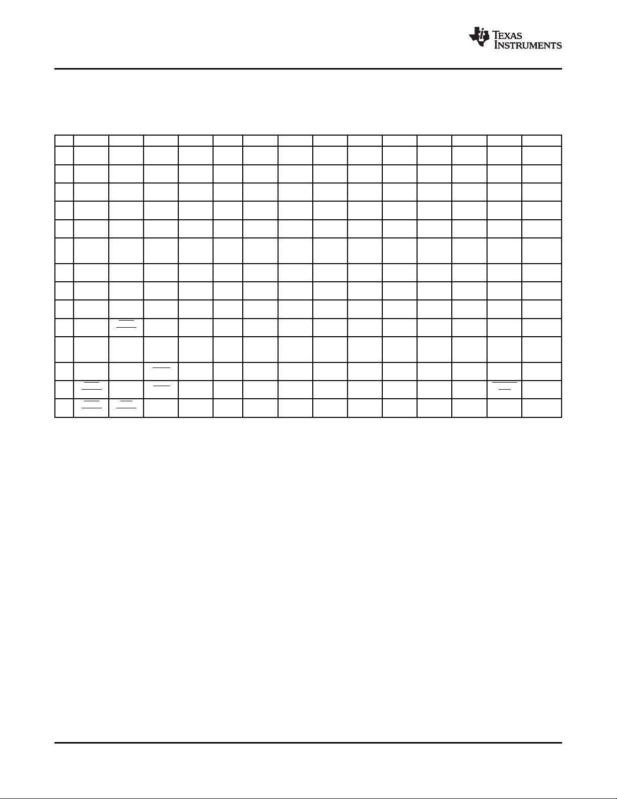
The XIO3130 is packaged in a 196-ball ZHC MicroStar™ BGA.
Table 2-1. XIO3130 Terminal Assignments
A B C D E F G H J K L M N P
14 GPIO12 SCL VDD15 GPIO4 VDD15 GPIO15 VDD15 VDD15
13 RSVD GPIO13 VDD15 SDA VDD15 VDD15 GPIO6 VDD15 GPIO7
12 GPIO2 RSVD GPIO3 VDD33 VSS VDD33 GPIO5 VDD15 GPIO14 GPIO16
11 VDD33 GPIO1 VDD15 VSS VSS VSS VSS VDD15 GPIO11 VDD33
VSSA DN1_ VSSA
10 VDD15 VSS VSS VSS VSS VSS VSS VSS VSS GPIO8 VDD15
(1) DPSTRP (3)
DN1_ DN1_
9 REFCK REFCK VSS VSS VSS VSS VSS VSS
Op On
DN1_ DN1_ VSSA VDDA15 VDDA15 VDDA15 VSSA
8 VSS VSS VSS VSS VSS VSS VDD15
PETp PETn (1) (1) (3) (3) (3)
VDDA15 VSSA VDDA15 VDDA15 VSSA DN3_ DN3_
7 VDD15 VSS VSS VSS VSS VSS VSS
(1) (1) (1) (3) (3) PETp PETn
DN1_ DN1_ VDDA15 VDDA15 VSSA DN3_
6 GPIO0 VSS VSS VSS VSS VSS VSS VSS
PERp PERn (3) (3) (3) REFCKOn
VSSA DN1_ VSSA DN3_
5 VDD15 VSS VSS VSS VSS VSS VSS VSS VSS VSS
(1) PERST (3) REFCKOp
4 VDD15 VDD33 RSVD RSVD COMB VDD15 VSS VDD33 VDD15
3 VDD33 VDD15 WAKE REFR1 VDD15 VDDA33 GPIO18 GPIO17 GPIO9 VDD15
DN2_ VDD33 UP_ VDDA15 UP_ UP_ CLKREQ
2 VDD15 GRST REFR0 VDD15 VSS VDD15 GPIO10
PERST REF PETn (0) PERn REFCKIn _UP
DN3_ UP_ VDD VSSD VAUX33 UP_ VSSA UP_ VSSA UP_
1 VDD15 VDD15 VDD33 RSVD
PERST PERST COMB15 REF REF PETp (0) PERp (0) REFCKIp
VSSA VDDA15 VSSA VSSA DN3_ DN3_
(1) (1) (3) (3) PERp PERn
VDD VDD15 VSSA VDDA15
COMBIO REF (0) (0)
VSSA DN2_ VSSA DN2_ DN2_ DN2_
(2) PERn (2) Petn REFCKOn REFCKOp
DN2_ DN2_ VSSA VSSA DN2_
PERp PETp (2) (2) DPSTRP
VSSA VDDA15 VSSA VDDA15
(2) (2) (2) (2)
VSSA VDDA15 VDDA15 VDDA15
(2) (2) (2) (2)
VSSA VDDA15 VDDA15 VDDA15 DN3_
REF (0) (0) (0) DPSTRP
VDD
33
www.ti.com
Introduction 14 Submit Documentation Feedback
Page 15

www.ti.com
SLLS693E – MAY 2007 – REVISED APRIL 2009
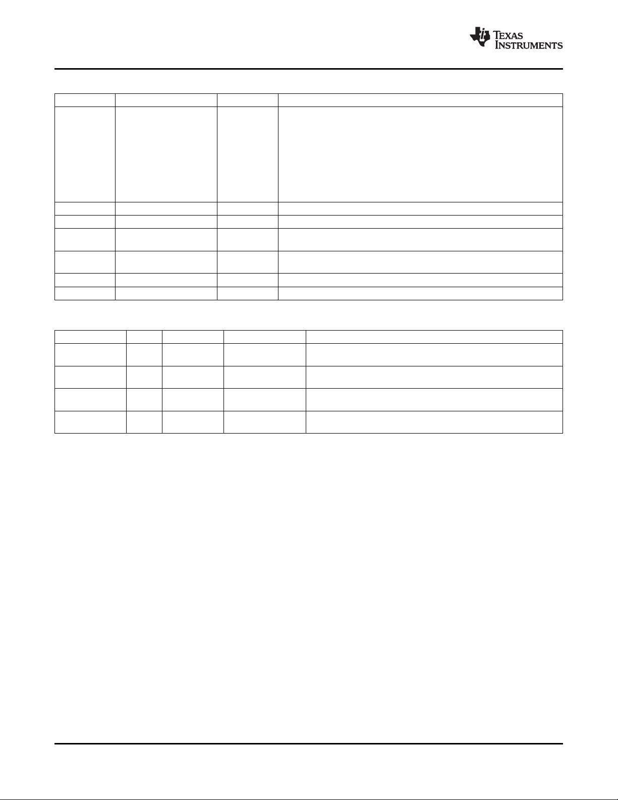
Table 2-2. XIO3130 Terminals Sorted Alphanumerically
Ball Signal Name Ball Signal Name Ball Signal Name Ball Signal Name Ball Signal Name
A01 DN3_PERST C13 VDD15 F11 VSSA(2) J08 VSS M06 VDDA15(3)
A02 DN2_PERST C14 VDD15 F12 VSSA(2) J09 VSS M07 VSSA(3)
A03 VDD33 D01 VSSDREF F13 DN2_PERp J10 VSS M08 VDDA15(3)
A04 VDD15 D02 REFR0 F14 DN2_PERn J11 VDDA15(2) M09 VSSA(3)
A05 VSSA(1) D03 VDDCOMBIO G01 UP_PETp J12 VDDA15(2) M10 GPIO8
A06 DN1_PERp D04 RSVD G02 UP_PETn J13 VSSA(2) M11 VDD15
A07 VDDA15(1) D05 VSS G03 VSSA(0) J14 DN2_REFCKOn M12 VDD15
A08 DN1_PETp D06 VSS G04 VDDA15(0) K01 VSSA(0) M13 GPIO6
A09 DN1_REFCKOp D07 VDDA15(1) G05 VSS K02 VSS M14 GPIO15
A10 VSSA(1) D08 VDDA15(1) G06 VSS K03 VDDA15(0) N01 VDD33
A11 VDD33 D09 VDDA15(1) G07 VSS K04 VDD15 N02 CLKREQ_UP
A12 GPIO2 D10 VSS G08 VSS K05 VSS N03 GPIO9
A13 RSVD D11 VSS G09 VSS K06 VSS N04 DN3_DPSTRP
A14 GPIO12 D12 VDD33 G10 VSS K07 VSS N05 VSSA(3)
B01 UP_PERST D13 SDA G11 VDDA15(2) K08 VSS N06 VSSA(3)
B02 VDD15 D14 GPIO4 G12 VDDA15(2) K09 VSS N07 DN3_PETp
B03 VDD15 E01 VAUX33REF G13 VDD15 K10 VSS N08 VDD15
B04 VDD33 E02 VDD33REF G14 VSSA(2) K11 VSS N09 DN3_PERp
B05 DN1_PERST E03 REFR1 H01 VSSA(0) K12 VDD33 N10 VDD15
B06 DN1_PERn E04 VSSAREF H02 VDDA15(0) K13 VSSA(2) N11 GPIO11
B07 VDD15 E05 VSS H03 VDD15 K14 DN2_REFCKOp N12 GPIO14
B08 DN1_PETn E06 VSS H04 VDDA15(0) L01 UP_REFCKIp N13 VDD15
B09 DN1_REFCKOn E07 VSS H05 VSS L02 UP_REFCKIn N14 VDD15
B10 VDD15 E08 VSS H06 VSS L03 GPIO18 P01 RSVD
B11 GPIO1 E09 VSS H06 VSS L04 VSS P02 GPIO10
B12 RSVD E10 VSS H07 VSS L05 VSS P03 VDD15
B13 GPIO13 E11 VSS H08 VSS L06 VDDA15(3) P04 VDD15
B14 SCL E12 VSS H09 VSS L07 VDDA15(3) P05 DN3_REFCKOp
C01 VDDCOMB15 E13 VDD15 H10 VSS L08 VDDA15(3) P06 DN3_REFCKOn
C02 GRST E14 VSSA(2) H11 VDDA15(2) L09 VSSA(3) P07 DN3_PETn
C03 WAKE F01 VDD15 H12 VSSA(2) L10 VSS P08 VSSA(3)
C04 RSVD F02 VDD15 H13 DN2_PETp L11 VSS P09 DN3_PERn
C05 VDD15 F03 VDD15REF H14 DN2_PETn L12 GPIO5 P10 VSSA(3)
C06 GPIO0 F04 VDDCOMB33 J01 UP_PERp L13 DN2_DPSTRP P11 VDD33
C07 VSSA(1) F05 VSS J02 UP_PERn L14 VDD15 P12 GPIO16
C08 VSSA(1) F06 VSS J03 VDDA33 M01 VDD15 P13 GPIO7
C09 VSSA(1) F07 VSS J04 VDDA15(0) M02 VDD15 P14 VDD15
C10 DN1_DPSTRP F08 VSS J05 VSS M03 GPIO17
C11 VDD15 F09 VSS J06 VSS M04 VDD33
C12 GPIO3 F10 VSS J07 VSS M05 VSS
XIO3130
Submit Documentation Feedback Introduction 15
Page 16

XIO3130
SLLS693E – MAY 2007 – REVISED APRIL 2009
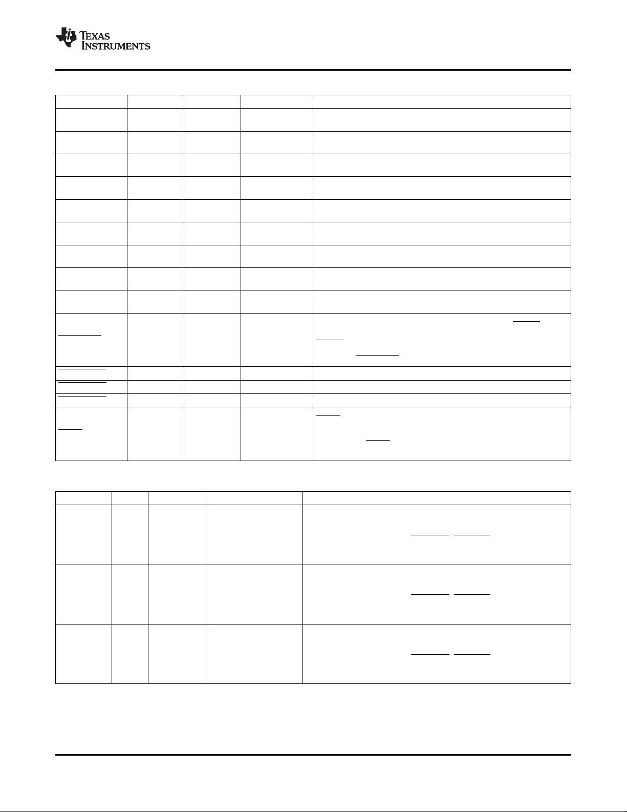
Table 2-3. XIO3130 Signal Names Sorted Alphabetically
Signal Name Ball Signal Name Ball
CLKREQ_UP N02 GPIO5 L12
DN1_DPSTRP C10 GPIO6 M13
DN1_PERn B06 GPIO7 P13
DN1_PERp A06 GPIO8 M10
DN1_PERST B05 GPIO9 N03
DN1_PETn B08 GRST C02
DN1_PETp A08 Suggested Program Value REFR0 D02
DN1_REFCKOn B09 REFR1 E03
DN1_REFCKOp A09 RSVD A13, B12, C04, D04, P01
DN2_DPSTRP L13 SCL B14
DN2_PERn F14 SDA D13
DN2_PERp F13 UP_PERn J02
DN2_PERST A02 UP_PERp J01
DN2_PETn H14 UP_PERST B01
DN2_PETp H13 UP_PETn G02
DN2_REFCKOn J14 UP_PETp G01
DN2_REFCKOp K14 UP_REFCKIn L02
DN3_DPSTRP N04 UP_REFCKIp L01
DN3_PERn P09 VAUX33REF E01
A04, B02, B03, B07, B10, C05, C11, C13,
DN3_PERp N09 VDD15
DN3_PERST A01 VDDA15(0) G04, H02, H04, J04, K03
DN3_PETn P07 VDDA15(1) A07, D07, D08, D09
DN3_PETp N07 VDDA15(2) G11, G12, H11, J11, J12
DN3_REFCKOn P06 VDDA15(3) L06, L07, L08, M06, M08
DN3_REFCKOp P05 VDD15REF F03
GPIO0 C06 VDD33 A03, A11, B04, D12, K12, M04, N01, P11
GPIO1 B11 VDD33REF E02
GPIO10 P02 VDDA33 J03
GPIO11 N11 VDDCOMB15 C01
GPIO12 A14 VDDCOMB33 F04
GPIO13 B13 VDDCOMBIO D03
GPIO14 N12 VSS H05, H06, H07, H08, H09, H10, J05, J06,
GPIO15 M14 VSSA(0) G03, H01, K01
GPIO16 P12 VSSA(1) A05, A10, C07, C08, C09
GPIO17 M03 VSSA(2) E14, F11, F12, G14, H12, J13, K13
GPIO18 L03 VSSA(3) L09, M07, M09, N05, N06, P08, P10
GPIO2 A12 VSSAREF E04
GPIO3 C12 VSSDREF D01
GPIO4 D14 WAKE C03
C14, E13, F01, F02, G13, H03, K04, L14,
M01, M02, M11, M12, N08, N10, N13, N14,
P03, P04, P14
D05, D06, D10, D11, E05, E06, E07, E08,
E09, E10, E11, E12, F05, F06, F07, F08,
F09, F10, G05, G06, G07, G08, G09, G10,
J07, J08, J09, J10, K02, K05, K06, K07,
K08, K09, K10, K11, L04, L05, L10, L11,
M05
www.ti.com
Introduction 16 Submit Documentation Feedback
Page 17

www.ti.com
SLLS693E – MAY 2007 – REVISED APRIL 2009
2.6 Terminal Descriptions
Table 2-4. Power Supply Terminals
Signal Ball I/O Type External parts Description
VDDA15(0) PWR Filter
VDDA15(1) A07, D07, D08, D09 PWR Filter
VDDA15(2) G11, G12, H11, J11, J12 PWR Filter
VDDA15(3) L06, L07, L08, M06, M08 PWR Filter
VDD15 G13, H03, K04, L14, PWR 1.5-V digital core power terminals
VDD33 PWR 3.3-V digital I/O power terminals
VDDA33 J03 PWR Filter 3.3-V analog power terminal
VAUX33REF E01 PWR 3.3-V digital V
VDD15REF F03 PWR Filter 1.5-V PCI-Express reference power terminal
VDD33REF E02 PWR Filter 3.3-V PCI-Express reference power terminal
G04, H02, H04, J04, 1.5-V analog power terminals for PCI-Express upstream port
K03 0
1.5-V analog power terminals for PCI-Express downstream
port 1
1.5-V analog power terminals for PCI-Express downstream
port 2
1.5-V analog power terminals for PCI-Express downstream
port 3
A04, B02, B03, B07,
B10, C05, C11, C13,
C14, E13, F01, F02,
M01, M02, M11, M12,
N08, N10, N13, N14,
P03, P04, P14
A03, A11, B04, D12, Bypass
K12, M04, N01, P11 capacitors
Bypass
capacitors
Bypass
capacitors
power terminal
AUX
XIO3130
Table 2-5. Combined Power Terminals
Signal Ball I/O Type External Parts Description
Internally combined 3.3-V main and V
VDDCOMBIO D03 Passive Bypass capacitors
VDDCOMB33 F04 Passive Bypass capacitors
VDDCOMB15 C01 Passive Bypass capacitors
bypass capacitor filtering. Supplies all internal 3.3-V input and output
circuitry powered during D3 cold. Caution: Do not use this terminal to
supply external power to other devices.
Internally combined 3.3-V main and V
bypass capacitor filtering. Supplies all internal 3.3-V circuitry powered
during D3 cold. Caution: Do not use this terminal to supply external
power to other devices.
Internally combined 1.5-V main and V
bypass capacitor filtering. Supplies all internal 1.5-V circuitry powered
during D3 cold. Caution: Do not use this terminal to supply external
power to other devices.
AUX
AUX
AUX
power output for external
power output for external
power output for external
Submit Documentation Feedback Introduction 17
Page 18
XIO3130
SLLS693E – MAY 2007 – REVISED APRIL 2009
Table 2-6. Ground Terminals
Signal Ball I/O Type Description
D05, D06, D10, D11, E05,
E06, E07, E08, E09, E10,
E11, E12, F05, F06, F07,
F08, F09, F10, G05, G06,
VSS GND Digital ground terminals
VSSA(0) G03, H01, K01 GND Analog ground terminals for upstream Port 0
VSSA(1) A05, A10, C07, C08, C09 GND Analog ground terminals for downstream Port 1
VSSA(2) GND Analog ground terminals for downstream Port 2
VSSA(3) GND Analog ground terminals for downstream Port 3
VSSAREF E04 GND 1.5-V PCI-Express analog reference ground terminal
VSSDREF D01 GND 1.5-V PCI-Express digital reference ground terminal
Signal Ball I/O Type External Parts Description
UP_REFCKIp L01 Reference clock inputs. REFCKIp and REFCKIn comprise the
UP_REFCKIn L02 differential input pair for the 100-MHz system reference clock.
DN1_REFCKOp A09
DN1_REFCKOn B09
DN2_REFCKOp K14
DN2_REFCKOn J14
DN3_REFCKOp P05
DN3_REFCKOn P06
G07, G08, G09, G10,
H05, H06, H07, H08, H09,
H10, J05, J06, J07, J08,
J09, J10, K02, K05, K06,
K07, K08, K09, K10, K11,
L04, L05, L10, L11, M05
E14, F11, F12, G14, H12,
J13, K13
L09, M07, M09, N05, N06,
P08, P10
Table 2-7. PCI Express Reference Clock Terminals
HS DIFF IN
HS DIFF OUT 100 MHz differential reference clock outputs for downstream port 1
HS DIFF OUT 100 MHz differential reference clock outputs for downstream port 2
HS DIFF OUT 100 MHz differential reference clock outputs for downstream port 3
www.ti.com
Introduction 18 Submit Documentation Feedback
Page 19
XIO3130
www.ti.com
Table 2-8. PCI Express Terminals
Signal Ball I/O Type External Parts Description
UP_PETp G01 HS DIFF
UP_PETn G02 OUT
DN1_PETp A08 HS DIFF
DN1_PETn B08 OUT
DN2_PETp H13 HS DIFF
DN2_PETn H14 OUT
DN3_PETp N07 HS DIFF
DN3_PETn P07 OUT
UP_PERp J01
UP_PERn J02
DN1_PERp A06
DN1_PERn B06
DN2_PERp F13
DN2_PERn F14
DN3_PERp N09
DN3_PERn P09
REFR0 D02 External bias External reference resistor terminals for setting TX driver current. An
REFR1 E03 resistor external resistor is connected between these terminals.
HS DIFF IN High-speed differential receiver pair for upstream port 0
HS DIFF IN High-speed differential receiver pair for downstream port 1
HS DIFF IN High-speed differential receiver pair for downstream port 2
HS DIFF IN High-speed differential receiver pair for downstream port 3
Passive
Series capacitors High-speed differential transmit pair for upstream port 0
Series capacitors High-speed differential transmit pair for downstream port 1
Series capacitors High-speed differential transmit pair for downstream port 2
Series capacitors High-speed differential transmit pair for downstream port 3
SLLS693E – MAY 2007 – REVISED APRIL 2009
UP_PERST B01 LV CMOS IN
DN1_PERST B05 LV CMOS O Pulldown resistor PCI-Express reset output for downstream port 1.
DN2_PERST A02 LV CMOS O Pulldown resistor PCI-Express reset output for downstream port 2.
DN3_PERST A01 LV CMOS O Pulldown resistor PCI-Express reset output for downstream port 3.
WAKE C03 LV CMOS I/O
System-side identifies that the system power is stable. When logic low, the
pullup resistor PERST signal generates an internal power-on reset.
System-side PCI-Express link hierarchy’s main power rails and reference clocks.
pullup resistor
PCI-Express reset input. When logic high, the PERST signal
Note: The UP_PERST input buffer has hysteresis.
WAKE is an active low signal that is driven low to reactivate the
Note: Since WAKE is an open-drain output buffer, a system-side
pullup resistor is required.
Table 2-9. PCI Hot Plug Strapping Terminals
Signal Ball I/O Type External Parts Description
Downstream Port 1 Strap. This pin is pulled high at the de-assertion of
DN1_DPSTR Pullup or pulldown for downstream port 1 and are no longer available for use as GPIOs.
P resistor The three terminals become PRESENT, PWR_ON, and PWR_GOOD
DN2_DPSTR Pullup or pulldown for downstream port 2 and are no longer available for use as GPIOs.
P resistor The three terminals become PRESENT, PWR_ON, and PWR_GOOD
DN3_DPSTR Pullup or pulldown for downstream port 3 and are no longer available for use as GPIOs.
P resistor The three terminals become PRESENT, PWR_ON, and PWR_GOOD
C10 LV CMOS IN
L13 LV CMOS IN
N04 LV CMOS IN
reset. GPIO0, GPIO1, and GPIO2 are used as PCI Hot Plug terminals
respectively. These GPIOs are available for normal use if this terminal
is pulled low at the de-assertion of reset.
Downstream Port 2 Strap. This pin is pulled high at the de-assertion of
reset. GPIO4, GPIO5, and GPIO6 are used as PCI Hot Plug terminals
respectively. These GPIOs are available for normal use if this terminal
is pulled low at the de-assertion of reset.
Downstream Port 3 Strap. This pin is pulled high at the de-assertion of
reset. GPIO8, GPIO9, and GPIO10 are used as PCI Hot Plug terminals
respectively. These GPIOs are available for normal use if this terminal
is pulled low at the de-assertion of reset.
Submit Documentation Feedback Introduction 19
Page 20
XIO3130
SLLS693E – MAY 2007 – REVISED APRIL 2009
Table 2-10. GPIO Terminals
Signal Ball I/O Type External Parts Description
GPIO 0. If the DN1_DPSTRP pin is pulled high at the de-assertion of
GPIO0 C06 LV CMOS I/O
GPIO1 B11 LV CMOS I/O
GPIO2 A12 LV CMOS I/O
GPIO3 C12 LV CMOS I/O
GPIO4 D14 LV CMOS I/O
GPIO5 L12 LV CMOS I/O
GPIO6 M13 LV CMOS I/O
GPIO7 P13 LV CMOS I/O
GPIO8 M10 LV CMOS I/O
GPIO9 N03 LV CMOS I/O
GPIO10 P02 LV CMOS I/O
GPIO11 N11 LV CMOS I/O
GPIO12 A14 LV CMOS I/O
GPIO13 B13 LV CMOS I/O
GPIO14 N12 LV CMOS I/O
GPIO15 M14 LV CMOS I/O
GPIO16 P12 LV CMOS I/O
GPIO17 M03 LV CMOS I/O
GPIO18 L03 LV CMOS I/O
reset, this pin functions as the PRSNT hotplug pin for downstream
port 1. Otherwise this pin’s function is programmed with the GPIO A
Control register.
GPIO 1. If the DN1_DPSTRP pin is pulled high at the de-assertion of
reset, this pin functions as the POWERON hotplug pin for
downstream port 1. Otherwise this pin’s function is programmed with
the GPIO A Control register.
GPIO 2. If the DN1_DPSTRP pin is pulled high at the de-assertion of
reset, this pin functions as the PWRGD hotplug pin for downstream
port 1. Otherwise this pin’s function is programmed with the GPIO A
Control register
GPIO 3. This pin’s function is programmed with the GPIO A Control
register.
GPIO 4. If the DN2_DPSTRP pin is pulled high at the de-assertion of
reset, this pin functions as the PRSNT hotplug pin for downstream
port 2. Otherwise this pin’s function is programmed with the GPIO A
Control register.
GPIO 5. If the DN2_DPSTRP pin is pulled high at the de-assertion of
reset, this pin functions as the POWERON hotplug pin for
downstream port 2. Otherwise this pin’s function is programmed with
the GPIO A Control register.
GPIO 6. If the DN2_DPSTRP pin is pulled high at the de-assertion of
reset, this pin functions as the PWRGD hotplug pin for downstream
port 2. Otherwise this pin’s function is programmed with the GPIO A
Control register.
GPIO 7. This pin’s function is programmed with the GPIO A Control
register.
GPIO 8. If the DN3_DPSTRP pin is pulled high at the de-assertion of
reset, this pin functions as the PRSNT hotplug pin for downstream
port 3. Otherwise this pin’s function is programmed with the GPIO B
Control register.
GPIO 9. If the DN3_DPSTRP pin is pulled high at the de-assertion of
reset, this pin functions as the POWERON hotplug pin for
downstream port 3. Otherwise this pin’s function is programmed with
the GPIO B Control register.
GPIO 10. If the DN3_DPSTRP pin is pulled high at the de-assertion
of reset, this pin functions as the PWRGD hotplug pin for
downstream port 3. Otherwise this pin’s function is programmed with
the GPIO B Control register.
GPIO 11. This pin’s function is programmed with the GPIO B Control
register.
GPIO 12. This pin’s function is programmed with the GPIO B Control
register.
GPIO 13. This pin’s function is programmed with the GPIO B Control
register.
GPIO 14. This pin’s function is programmed with the GPIO B Control
register.
GPIO 15. This pin’s function is programmed with the GPIO B Control
register.
GPIO16. This pin’s function is programmed with the GPIO C Control
register.
GPIO 17. This pin’s function is programmed with the GPIO C Control
register.
GPIO 18. This pin’s function is programmed with the GPIO C Control
register.
www.ti.com
Introduction 20 Submit Documentation Feedback
Page 21
www.ti.com
SLLS693E – MAY 2007 – REVISED APRIL 2009
Table 2-11. Miscellaneous Terminals
Signal Ball I/O Type External Parts Description
GRST See description VDD3.3 (if not) is required unless this terminal is always driven by
SDA D13 LV CMOS I/O Serial Data. This pin is the serial data pin for the EEPROM interface.
SCL
CLKREQ_UP device restart clock in cases where upstream clock may be removed
RSVD A13, B12, Reserved. These terminals must tied to VDD15.
RSVD C04, P01 Reserved. This terminal must be tied to GND.
RSVD D04 See description Reserved. Pullup to Vaux (if supported) or VDD3.3 (if not)
C02 LV CMOS IN Global power-on reset input. Note: a pullup to Vaux (if supported) or
the upstream device.
B14 LV CMOS O Serial Clock. This pin is the serial clock pin for the EEPROM
interface.
N02 LV CMOS O Upstream Clock Request. When asserted low, requests upstream
in L1
XIO3130
Submit Documentation Feedback Introduction 21
Page 22
PCI
Express
X1 Phy
Port0
(Up)
Logic
Virtual
PCIto
PCI
Bridge
Port1
(Down)
Logic
Port2
(Down)
Logic
Port3
(down)
logic
GPIO
PCI Hot
Plug
EEPROM
Clock
Distribution/
ResetLogic
Virtual
PCIto
PCIBridge
Bridge
Virtual
PCIto
PCIBridge
Bridge
Virtual
PCIto
PCIBridge
Bridge
PCI
Expressx1
Phy
PCI
Expressx1
Phy
PCI
Expressx1
Phy
XIO3130
SLLS693E – MAY 2007 – REVISED APRIL 2009
3 Description
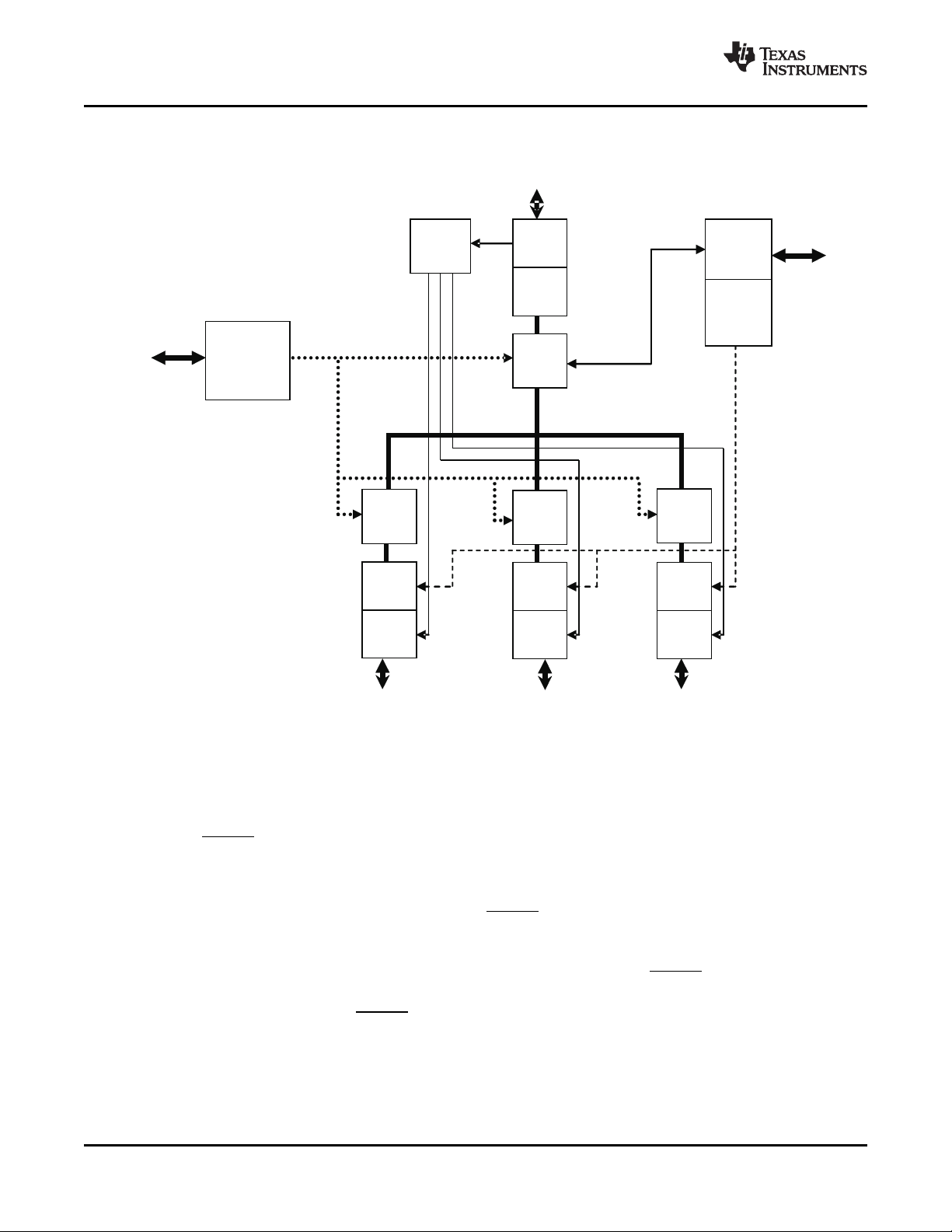
Figure 3-1 is the block diagram of the XIO3130.
www.ti.com
3.1 Power-Up/Power-Down Sequencing
The following sections describe the procedures to power up and power down the XIO3130 switch.
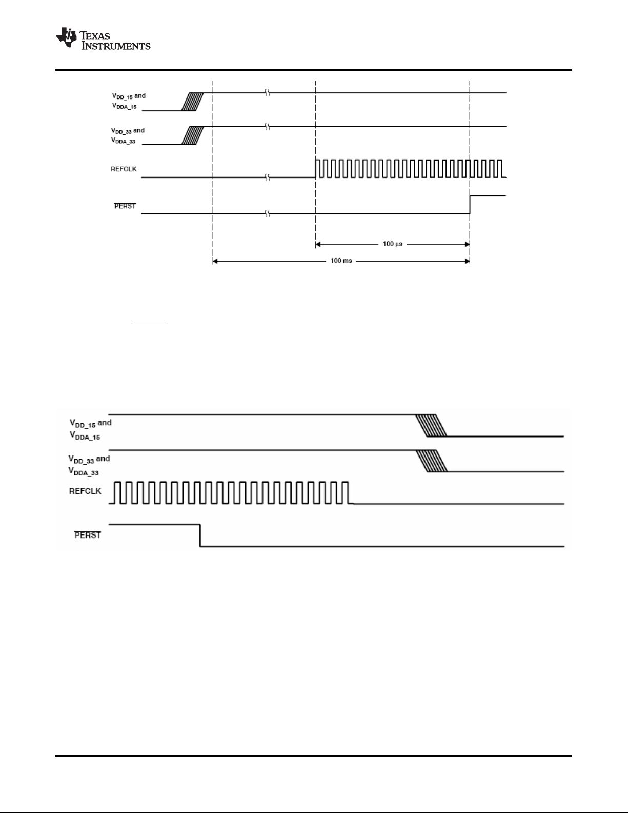
3.1.1 Power-Up Sequence
1. Assert PERST to the device.
2. Apply 1.5-V and 3.3-V voltages in any order with any time relationship and with any ramp rate.
3. Apply a stable PCI Express reference clock.
To meet PCI Express specification requirements, PERST cannot be de-asserted until the following two
delay requirements are satisfied:
• Wait a minimum of 100 µ s after applying a stable PCI Express reference clock. The 100- µ s limit
satisfies the requirement for stable device clocks by the de-assertion of PERST.
• Wait a minimum of 100 ms after applying power. The 100-ms limit satisfies the requirement for stable
power by the de-assertion of PERST.
See Figure 3-2 , Power-Up Sequence Diagram.
Description 22 Submit Documentation Feedback
Figure 3-1. Block Diagram
Page 23
www.ti.com
3.1.2 Power-Down Sequence
• Assert PERST to the device.
• Remove the reference clock.
• Remove 3.3-V and 1.5-V voltages.
XIO3130
SLLS693E – MAY 2007 – REVISED APRIL 2009
Figure 3-2. Power-Up Sequence Diagram
See the power-down sequence diagram in Figure 3-3 . If the VAUX33REF terminal is to remain powered
after a system shutdown, the switch power-down sequence is exactly the same as shown in Figure 3-3 .
3.2 Express Interface
3.2.1 External Reference Clock
The Texas Instruments XIO3130 switch requires a differential 100 MHz common clock reference. The
clock reference must meet all PCI Express electrical specification requirements for frequency tolerance,
spread spectrum clocking, and signal electrical characteristics.
Figure 3-3. Power-Down Sequence Diagram
3.2.2 Clock Generator
The clock generator is responsible for generating all internal and external clocks from the PCI Express
reference clock. This includes the PHY transmitter serial link clock, the three downstream reference clock
outputs, the 60-kHz serial bus interface clock, and all internal clock domains.
Submit Documentation Feedback Description 23
Page 24
XIO3130
SLLS693E – MAY 2007 – REVISED APRIL 2009
3.2.3 Beacon
The XIO3130 supports the PCI Express in-band beacon feature. Beacon is driven on the PCI Express link
by the XIO3130 to request the re-application of main power when in the L2 link state. Once beacon is
activated, the XIO3130 continues to send the beacon signal until main power is restored as indicated by
PERST going inactive. At this time, the beacon signal is deactivated.
3.2.4 WAKE
The XIO3130 supports the PCI Express sideband WAKE feature. WAKE is an active-low signal driven by
the XIO3130 to request the re-application of main power when in the L2 link state. Since WAKE is an
open-collector output, a system-side pullup resistor is required to prevent the signal from floating. If WAKE
to Beacon translation is enabled (see section 3.2.60), the XIO3130 detects when WAKE is asserted and
transmits beacon to alert the system. This enables support for devices that use the WAKE protocol in a
system that does not support it.
3.2.5 Initial Flow Control Credits
The XIO3130 flow control credits are initialized using the rules defined in the PCI Express Base
Specification. Table 3-1 identifies the initial flow control credit advertisement for the XIO3130. The initial
advertisement is exactly the same for both upstream and downstream ports.
Posted Request Headers (PH) 10 16
Posted Request Data (PD) 80 128
Non-Posted Header (NPH) 10 16
Non-Posted Data (NPD) 10 16
Completion Header (CPLH) 10 16
Completion Data (CPLD) 80 128
Table 3-1. Initial Flow Control Credit Advertisements
Credit Type
www.ti.com
Initial Advertisement
Hex Decimal
3.2.6 PCI Express Message Transactions
PCI Express messages are initiated by, received by and passed through the XIO3130. Table 3-2 outlines
message support within the switch.
Description 24 Submit Documentation Feedback
Page 25

www.ti.com
Table 3-2. Messages Supported by the XIO3130
Message Supported XIO3130 Action
Assert_INTx Yes Passed through upstream
Deassert_INTx Yes Passed through upstream
PM_Active_State_Nak Yes Received and processed
PM_PME Yes
PME_Turn_Off Yes
PME_TO_Ack Yes
ERR_COR Yes
ERR_NONFATAL Yes
ERR_FATAL Yes
Unlock Yes
Set_Slot_Power_Limit Yes
Advanced Switching Messages No Discarded
Vendor Defined Type 0 Yes
Vendor Defined Type 1 Yes
Passed through upstream
Downstream PCI Hot Plug Event: Initiated upstream
Received and processed
Passed through downstream
Downstream port: Received and processed
Downstream ports: Initiated upstream
Passed through upstream
Initiated upstream
Passed through upstream
Initiated upstream
Passed through upstream
Initiated upstream
Received and processed
Passed through downstream
Upstream port: Received and processed
Downstream port: Initiated downstream
Upstream port: Unsupported request
Passed through downstream
Upstream port: Discarded
Passed through downstream
XIO3130
SLLS693E – MAY 2007 – REVISED APRIL 2009
3.3 GPIO Terminals
3.4 Serial EEPROM
All supported message transactions are processed according to the PCI Express Base Specification.
Up to 19 general-purpose input/output (GPIO) terminals are provided for system customization. These
GPIO terminals are 3.3-V tolerant.
The exact number of GPIO terminals available varies based on the implementation of various supported
functions that share GPIO terminals. When any of the shared functions are enabled, the associated GPIO
terminal is disabled. When pulled high, the DPSTRP terminals cause some GPIO terminals to be mapped
to PCI Hot Plug functions for specific ports. Additional information can be found in the DPSTRP pin
descriptions and in Chapter 4.
All GPIO terminals are individually configurable as either inputs or outputs by writing the corresponding
bits in the GPIOA, GPIOB, GPIOC, or GPIOD Control Registers. The GPIO data register is used to
monitor GPIO terminals defined as inputs or to set the state of GPIO terminals defined as outputs. For
more information on GPIO terminals, see sections Section 4.2.61 through Section 4.2.65 .
The XIO3130 provides a two-wire serial-bus interface to load subsystem identification information and
specific register defaults from an external EEPROM. This interface supports slow, fast, and high-speed
EEPROM speed options.
Submit Documentation Feedback Description 25
Page 26
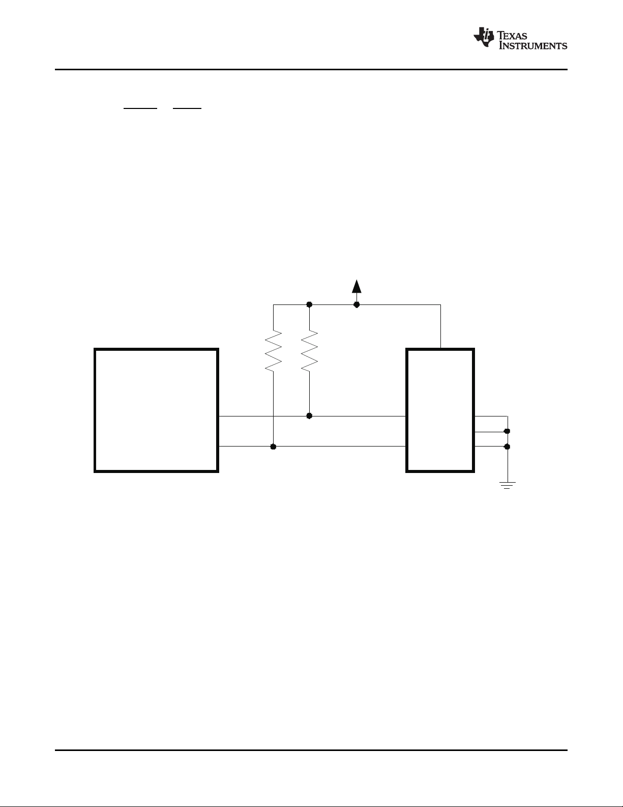
XIO3130
SCL
SDA
SERIAL
EEPROM
SCL A2
A1
SDA A0
VDD33
XIO3130
SLLS693E – MAY 2007 – REVISED APRIL 2009
3.4.1 Serial Bus Interface Implementation
To enable the serial bus interface, a pullup resistor must be implemented on the SDA signal. At the rising
edge of PERST or GRST, whichever occurs last, the SDA terminal is checked for a pullup resistor. If one
is detected, bit 3 (SBDETECT) in the serial bus control and status register (see Table 4-32 ) is set.
Software may disable the serial bus interface at any time by writing a zero to the SBDETECT bit. If no
external EEPROM is required, the serial bus interface is permanently disabled by attaching a pulldown
resistor to the SDA signal.
The XIO3130 implements a two-terminal serial interface with one clock signal (SCL) and one data signal
(SDA). The SCL signal is a unidirectional output from the XIO3130 and the SDA signal is bidirectional.
Both are open-drain signals and require pullup resistors. The XIO3130 is a bus master device and drives
SCL at approximately 60 kHz during data transfers and places SCL in a high-impedance state during bus
idle states. The serial EEPROM is a bus slave device and must acknowledge a slave address equal to
1010_000X binary. Figure 3-4 illustrates a sample application implementing the two-wire serial bus.
www.ti.com
3.4.2 Serial Bus Interface Protocol
All data transfers are initiated by the serial bus master. The beginning of a data transfer is indicated by a
start condition, which is signaled when the SDA line transitions to a low state while SCL is in the high
state, as illustrated in Figure 3-5 . The end of a requested data transfer is indicated by a stop condition,
which is signaled by a low-to-high transition of SDA while SCL is in the high state, as shown in Figure 3-5 .
Data on SDA must remain stable during the high state of the SCL signal because changes on the SDA
signal during the high state of SCL are interpreted as control signals (i.e., a start or a stop condition).
Description 26 Submit Documentation Feedback
Figure 3-4. Serial EEPROM Applications
Page 27
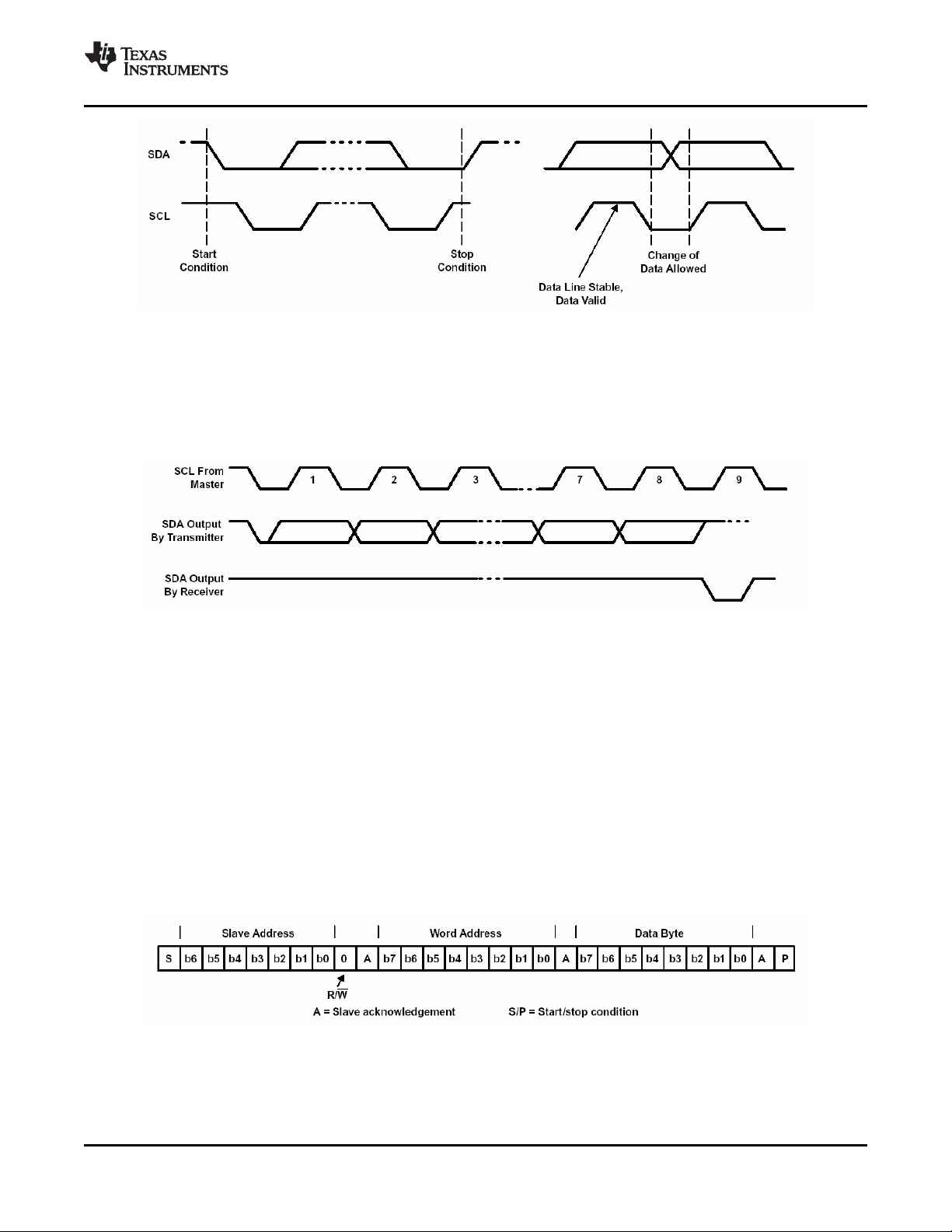
XIO3130
www.ti.com
Figure 3-5. Serial-Bus Start/Stop Conditions and Bit Transfers
Data is transferred serially in 8-bit bytes. During a data transfer operation, an unlimited number of bytes
are transmitted. However, each byte must be followed by an acknowledge bit to continue the data transfer
operation. An acknowledge (ACK) is indicated by the data byte receiver pulling the SDA signal low, so that
it remains low during the high state of the SCL signal. Figure 3-6 illustrates the acknowledge protocol.
SLLS693E – MAY 2007 – REVISED APRIL 2009
Figure 3-6. Serial-Bus Protocol Acknowledge
The XIO3130 performs three basic serial bus operations: single-byte reads, single-byte writes, and
multiple-byte reads. The single-byte operations occur under software control. The multiple-byte read
operations are performed by the serial EEPROM initialization circuitry immediately after a PCI Express
Reset. For details on how the XIO3130 automatically loads the subsystem identification and other register
defaults from the serial-bus EEPROM, see Section 3.4.3 , Serial Bus EEPROM Application.
Figure 3-7 illustrates a single-byte write. The XIO3130 issues a start condition and sends the 7-bit slave
device address and the R/W command bit equal to zero. A zero in the R/W command bit indicates that the
data transfer is a write. The slave device acknowledges that it recognizes the slave address. If the
XIO3130 receives no acknowledgment, the SB_ERR status bit is set in the serial-bus control and status
register (PCI offset B3h; see Table 4-32 ). Next, the XIO3130 sends the EEPROM word address, and
another slave acknowledgment is expected. Then the XIO3130 delivers the data byte (MSB first) and
expects a final acknowledgment before issuing the stop condition.
Figure 3-7. Serial-Bus Protocol – Byte Write
Figure 3-8 illustrates a single-byte read. The XIO3130 issues a start condition and sends the 7-bit slave
device address and the R/W command bit equal to zero (write). The slave device acknowledges that it
recognizes the slave address. Next, the XIO3130 sends the EEPROM word address, and another slave
Submit Documentation Feedback Description 27
Page 28
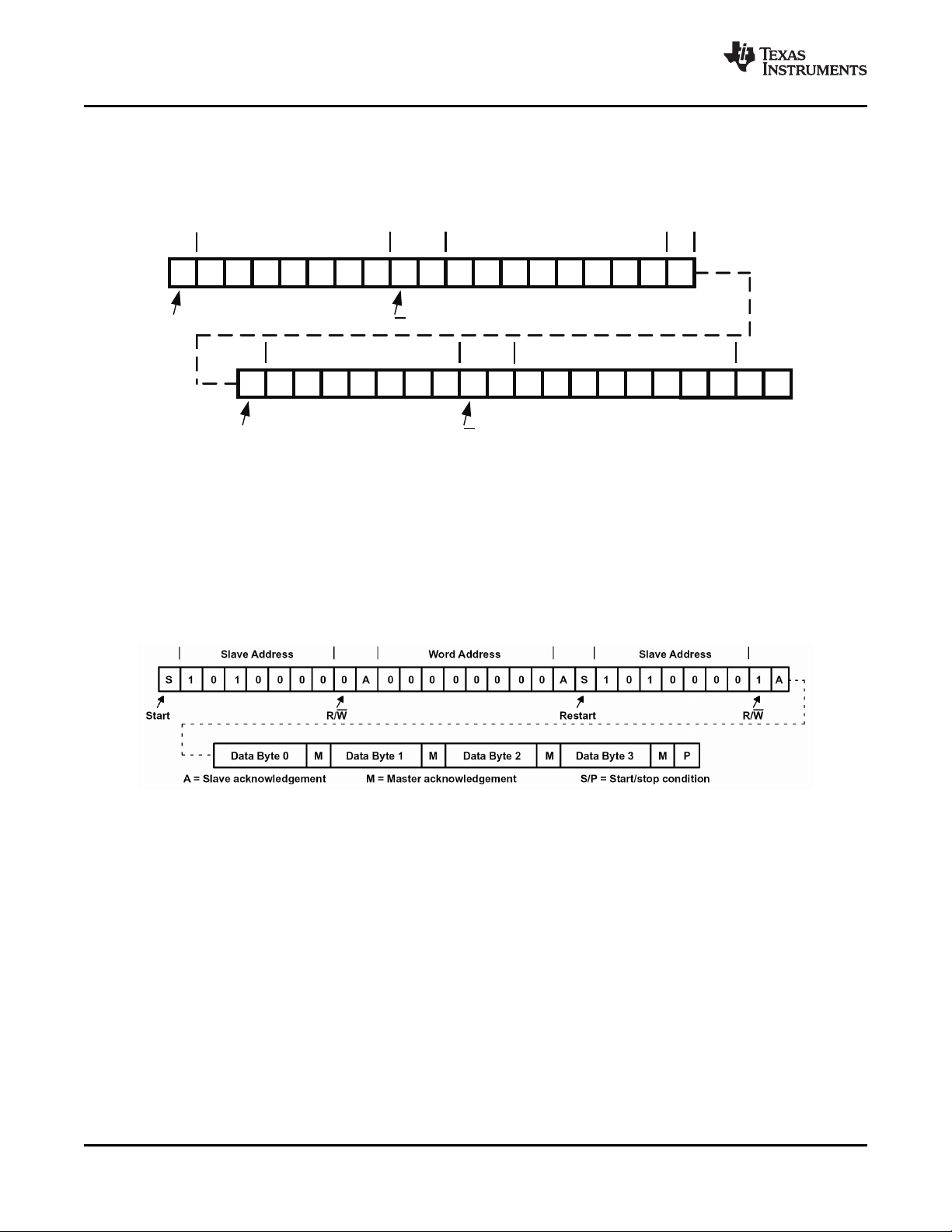
S
b6 b1b2b3b4b5 b0 1 A
b7 b6 b1b2b3b4b5 b0 A
Slave Address
Word Address
Start
R/W
S
Restart
b6 b1b2b3b4b5 b0 0 A
Slave Address
R/W
b7 b6 b1b2b3b4b5 b0 M
DataByte
P
A =Slave AcknowledgementM=Master AcknowledgementS/P =Start/StopCondition
XIO3130
SLLS693E – MAY 2007 – REVISED APRIL 2009
acknowledgment is expected. Then, the XIO3130 issues a restart condition followed by the 7-bit slave
address and the R/W command bit equal to one (read). Once again, the slave device responds with
acknowledge. Next, the slave device sends the 8-bit data byte, MS bit first. Since this is a one-byte read,
the XIO3130 responds with no acknowledge (logic high), indicating the last data byte. Finally, the XIO3130
issues a stop condition.
Figure 3-9 illustrates the serial interface protocol during a multiple-byte serial EEPROM download. The
serial bus protocol starts exactly the same way as a one-byte read. The only difference is that multiple
data bytes are transferred. The number of transferred data bytes is controlled by the XIO3130 master.
After each data byte, if more data bytes are requested, the XIO3130 master issues acknowledge (logic
low). The transfer ends after an XIO3130 master no acknowledge (logic high), followed by a stop
condition.
www.ti.com
Figure 3-8. Serial-Bus Protocol – Byte Read
Figure 3-9. Serial-Bus Protocol – Multiple-Byte Read
The PROT_SEL bit (bit 7) in the Serial Bus Control and Status register changes the serial bus protocol.
Each of the three previous serial-bus protocol figures illustrates the PROT_SEL bit default (logic low).
When this control bit is asserted, the word address and corresponding acknowledge are removed from the
serial bus protocol. This feature allows the system designer a second serial bus protocol option when
selecting external EEPROM devices.
3.4.3 Serial Bus EEPROM Application
The registers and corresponding bits that are loaded through the EEPROM are provided in Table 3-3 .
Note the following:
• EEPROM bytes 00h through 1Dh affect the general control options for the XIO3130.
• EEPROM bytes 1Eh through 27h affect the operation of the upstream port (port 0).
• Bytes 00h through 27h are loaded into the configuration registers for the upstream virtual bridge or port
0 (see Figure 4-1 ).
• EEPROM bytes 28h through 35h correspond to and are loaded into the configuration space for the first
downstream virtual bridge or port 1 (see Figure 4-1 ).
Description 28 Submit Documentation Feedback
Page 29

www.ti.com
• EEPROM bytes 36h through 43h correspond to and are loaded into the configuration space for the
second downstream virtual bridge or port 2 (see Figure 4-1 ).
• EEPROM bytes 44h through 51h correspond to and are loaded into the configuration space for the
third downstream virtual bridge or port 3 (see Figure 4-1 ).
Table 3-3. EEPROM Register Loading Map
EEPROM Byte Address Suggested Programmed CONFIG Register Address
(hex) Value (hex) (hex)
0 4C NA Global Switch/Upstream Port Function Indicator
1 0 NA TI Proprietary register
2 24 0B4 Upstream Port Link PM Latency register
3 0 0B5 Upstream Port Link PM Latency register
4 0 0B8 Global Chip Control register
5 0 0B9 Global Chip Control register
6 0 0BA Global Chip Control register
7 0 0BB Global Chip Control register
8 0 0BC GPIOA register
9 0 0BD GPIOA register
0A 0 0BE GPIOB register
0B 0 0BF GPIOB register
0C 0 0C0 GPIOC register
0D 0 0C1 GPIOC register
0E 0 0C2 GPIOD register
0F 0 0C3 GPIOD register
10 0 0C4 GPIO Data register
11 0 0C5 GPIO Data register
12 0 0C6 GPIO Data register
13 0 0C7 GPIO Data register
14 01 0C8 TI Proprietary register
15 0 0CC TI Proprietary register
16 0 0CD TI Proprietary register
17 0 0D0 TI Proprietary register
18 0 0D1 TI Proprietary register
19 14 0D2 TI Proprietary register
1A 32 0D3 TI Proprietary register
1B 2 0DC TI Proprietary register
1C 0 0DE TI Proprietary register
1D 0 0DF TI Proprietary register
1E 0 NA Global Switch/Upstream Port 0 Function Indicator
1F 0 NA Not used
20 XX 0E0 Subsystem Access Vendor ID register
21 XX 0E1 Subsystem Access Vendor ID register
22 XX 0E2 Subsystem Access Subsys ID register
23 XX 0E3 Subsystem Access Subsys ID register
24 0 0E4 General Control register
25 24 0E8 Downstream Port Link PM Latency register
26 3F 0E9 Downstream Port Link PM Latency register
27 4 0EA Global Switch Control register
28 1 NA Downstream Port 1 Function Indicator
(1) Required program value
XIO3130
SLLS693E – MAY 2007 – REVISED APRIL 2009
Register Description
(1)
(1)
(1)
(1)
(1)
(1)
(1)
(1)
(1)
(1)
(1)
(1)
Submit Documentation Feedback Description 29
Page 30

XIO3130
SLLS693E – MAY 2007 – REVISED APRIL 2009
Table 3-3. EEPROM Register Loading Map (continued)
EEPROM Byte Address Suggested Programmed CONFIG Register Address
(hex) Value (hex) (hex)
29 0 NA Not used
2A 01 0C8 TI Proprietary register
2B 0 0CC TI Proprietary register
2C 0 0CD TI Proprietary register
2D 0 0D0 TI Proprietary register
2E 0 0D1 TI Proprietary register
2F 14 0D2 TI Proprietary register
30 32 0D3 TI Proprietary register
31 10 0D4 General Control register
32 60 0D5 General Control register
33 1A 0EC L0s Timeout register
34 0 0EE General Slot Info register
35 0 0EF General Slot Info register
36 2 NA Downstream Port 2 Function Indicator
37 0 NA Not used
38 01 0C8 TI Proprietary register
39 0 0CC TI Proprietary register
3A 0 0CD TI Proprietary register
3B 0 0D0 TI Proprietary register
3C 0 0D1 TI Proprietary register
3D 14 0D2 TI Proprietary register
3E 32 0D3 TI Proprietary register
3F 10 0D4 General Control register
40 60 0D5 General Control register
41 1A 0EC L0s Timeout register
42 0 0EE General Slot Info register
43 0 0EF General Slot Info register
44 2 NA Downstream Port 3 Function Indicator
45 0 NA Not used
46 01 0C8 TI Proprietary register
47 0 0CC TI Proprietary register
48 0 0CD TI Proprietary register
49 0 0D0 TI Proprietary register
4A 0 0D1 TI Proprietary register
4B 14 0D2 TI Proprietary register
4C 32 0D3 TI Proprietary register
4D 10 0D4 General Control register
4E 60 0D5 General Control register
4F 1A 0EC L0s Timeout register
50 0 0EE General Slot Info register
51 0 0EF General Slot Info register
www.ti.com
Register Description
(1)
(1)
(1)
(1)
(1)
(1)
(1)
(1)
(1)
(1)
(1)
(1)
(1)
(1)
(1)
(1)
(1)
(1)
(1)
(1)
(1)
Description 30 Submit Documentation Feedback
Page 31

www.ti.com
This download table must be explicitly followed for the XIO3130 to correctly load initialization values from
a serial EEPROM. All byte locations must be considered when programming the EEPROM.
The XIO3130 addresses the serial EEPROM using a default slave address of 1010_000X binary. For an
EEPROM download operation that occurs immediately after PERST, this address is fixed. The serial
EEPROM in the sample application circuit (Figure 3-4 ) assumes the 1010b high-address nibble. The lower
three address bits are terminal inputs to the chip, and the sample application shows these terminal inputs
tied to VSS to match the least-significant three address bits.
During an EEPROM download operation, bit 4 (ROMBUSY) in the serial-bus control and status register is
asserted. After the download is finished, bit 4 is negated. At that time, bit 0 (ROM_ERR) in the serial-bus
control and status register may be monitored to verify a successful download.
3.4.4 Accessing Serial Bus Devices Through Software
The XIO3130 provides a programming mechanism to control serial bus devices through system software.
The programming is accomplished through a doubleword of PCI configuration space at offset B0h.
Table 3-4 lists the registers used to program a serial-bus device through software.
Table 3-4. Register for Programming Serial-Bus Devices
PCI Offset Register Name Description
B0h Serial-bus data
B1h Serial-bus word address writes or reads. This register is not used in the quick command
B2h Serial-bus slave address The slave device address and the R/W command selector are
B3h Control and Status through this register. In addition, the protocol-select bit and serial
XIO3130
SLLS693E – MAY 2007 – REVISED APRIL 2009
This register contains the data byte to send on write commands or
the received data byte on read commands.
The content of this register is sent as the word address on byte
protocol.
Write transactions to this register initiate a serial-bus transaction.
programmed through this register.
Serial interface enable, busy, and error status are communicated
bus test bit are programmed through this register.
To access the serial EEPROM through the software interface, the software performs five steps:
1. Reads the Control and Status Byte to verify that the EEPROM interface is enabled (SBDETECT
asserted) and not busy (REQBUSY and ROMBUSY negated).
2. Loads the Serial Bus word address. If the access is a write, the data byte is also loaded.
3. Writes the Serial Bus slave address and read/write command selector byte.
4. Monitors REQBUSY until this bit is negated.
5. Checks SB_ERR to verify that the serial bus operation completed without error. If the operation is a
read, after REQBUSY is negated, the serial bus data byte is valid.
3.5 Switch Reset Features
Four XIO3130 reset options are available:
• Internally-generated power-on reset
• A global reset generated by asserting GRST input terminal
• A PCI Express reset generated by asserting PERST input terminal
• Software-initiated resets that are controlled by sending a PCI Express training control hot reset
Table 3-5 identifies these reset sources and describes how the XIO3130 responds to each reset.
Submit Documentation Feedback Description 31
Page 32

XIO3130
SLLS693E – MAY 2007 – REVISED APRIL 2009
Table 3-5. Switch Reset Options
Reset Option XIO3130 Feature Reset Response
Internally-generated power-on During a power-on cycle, the XIO3130 asserts an When the internal power-on reset is asserted, all
reset internal reset and monitors the VDDCOMB15 (C01) control registers, state machines, sticky register bits,
Global reset input GRST (C02) When GRST is asserted low, an internal power-on When GRST is asserted low, all control registers,
PCI Express reset input When PERST is asserted low, all control register
PERST (B01) bits that are not sticky are reset. Also, all state
PCI Express training control The XIO3130 responds to a training control hot In the DL_DOWN state, all remaining configuration
hot reset reset received on the PCI Express interface. After a register bits and state machines are reset. All
terminal. When this terminal reaches 90% of the and power management state machines are
nominal input voltage specification, power is initialized to their default state.
considered stable. After stable power, the XIO3130
monitors the PCI Express reference clock
(REFCLKI) and waits 10 µ s after active clocks are
detected. Then, internal power-on reset is
de-asserted.
reset occurs. This reset is asynchronous and state machines, sticky register bits, and power
functions during both normal power states and V
power states. default state. When the rising edge of GRST occurs,
This XIO3130 input terminal is used by an upstream
PCI Express device to generate a PCI Express reset
and to signal a system power good condition.
When PERST is asserted low, all control register
bits that are not sticky are reset. Also, all state
machines that are not associated with sticky
functionality or VAUX power management are reset.
When the rising edge of PERST occurs, the switch
samples the state of all static control inputs and
latches the information internally. If an external
serial EEPROM is detected, then a download cycle
is initiated. Also, the process to configure and
initialize the PCI Express link is started. The switch
starts link training within 80 ms after PERST or
GRST is de-asserted.
Note: The system must assert PERST before power
is removed, before REFCLKI is removed, or before
REFCLKI becomes unstable.
training control hot reset, the PCI Express interface remaining bits exclude sticky bits and EEPROM
enters the DL_DOWN state. loadable bits. All remaining state machines exclude
management state machines are initialized to their
AUX
the switch samples the state of all static control
inputs and latches the information internally. If an
external serial EEPROM is detected, then a
download cycle is initiated. Also, the process to
configure and initialize the PCI Express link is
started. The switch starts link training within 80 ms
after PERST or GRST is de-asserted.
machines that are not associated with sticky
functionality or V
When the rising edge of PERST occurs, the switch
samples the state of all static control inputs and
latches the information internally. If an external
serial EEPROM is detected, then a download cycle
is initiated. Also, the process to configure and
initialize the PCI Express link is started. The switch
starts link training within 80 ms after PERST or
GRST is de-asserted.
sticky functionality, EEPROM functionality, and V
power management.
power management are reset.
AUX
www.ti.com
AUX
Description 32 Submit Documentation Feedback
Page 33

www.ti.com
4 XIO3130 Configuration Register Space
This chapter specifies the configuration registers that are used to enumerate the XIO3130 device within a
PC system.
An overview of the configuration register space is provided along with a detailed description of the register
bits associated with the upstream and downstream ports of the XIO3130.
4.1 PCI Configuration Register Space Overview
Each PCI Express port contains a set of PCI configuration registers. One of the upstream port registers,
the Global Chip Control register, is used to control functions across the entire XIO3130.
For downstream ports, only one register set is specified, but this register set is duplicated for each
downstream port. Figure 4-1 illustrates the enumeration topology.
The XIO3130 must appear as a hierarchy of PCI-to-PCI bridges in the manner outlined by the PCI
Express base specification.
This numbering scheme is typical but not ensured. Bus numbers are assigned within the
Type 01h configuration header during the initial enumeration of the PCI bus by the system
at power-up.
XIO3130
SLLS693E – MAY 2007 – REVISED APRIL 2009
NOTE
Submit Documentation Feedback XIO3130 Configuration Register Space 33
Page 34

**Examplevalues.Actualbusnumbers may change based on system hierarchy.
Virtual Internal PCI Bus
Downstream Port
Header Type 01h
PCI Capability
Structures /
Proprietary
Register Space
Extended
Configuration
Space / PCI Express
Capability Structures
000h
03Fh
040h
0FFh
100h
FFFh
Port# 1
Bus# N+2**
Downstream Port
Header Type 01h
PCI Capability
Structures /
Proprietary
Register Space
Extended
Configuration
Space / PCI Express
Capability Structures
000h
03Fh
040h
0FFh
100h
FFFh
Port# 2
Bus# N+3**
Downstream Port
Header Type 01h
PCI Capability
Structures /
Proprietary
Register Space
Extended
Configuration
Space / PCI Express
Capability Structures
000h
03Fh
040h
0FFh
100h
FFFh
Port# 3
Bus# N+4**
Upstream Port
Header Type 01h
PCI Capability
Structures /
Proprietary
Register Space
Extended
Configuration
Space / PCI Express
Capability Structures
000h
03Fh
040h
0FFh
100h
FFFh
Device# 0
Bus# N**
Device# 0 Device# 1 Device# 2
(Bus# N+1**)
Port# 0
XIO3130
SLLS693E – MAY 2007 – REVISED APRIL 2009
www.ti.com
4.2 PCI Express Upstream Port Registers
The default reset domain for all upstream port registers is IPRST. The internal IPRST reset signal is
asserted when the internally-generated power-on reset is asserted, when GRST is asserted, when PERST
is asserted, or when PCI Express training control hot reset is asserted. Some register fields are placed in
a reset domain different from the default reset domain; all bit or field descriptions identify any unique reset
domains. Generally, all sticky bits are placed in the GRST domain and all (non-sticky) EEPROM loadable
bits are placed in the PERST domain.
XIO3130 Configuration Register Space34 Submit Documentation Feedback
Figure 4-1. XIO3130 Enumerations Topology
Page 35

www.ti.com
SLLS693E – MAY 2007 – REVISED APRIL 2009
4.2.1 PCI Configuration Space (Upstream Port) Register Map
Table 4-1. PCI Express Upstream Port Configuration Register Map (Type 1)
Register Name Offset
Device ID Vendor ID 000h
Status Command 004h
Class Code Revision ID 008h
BIST Header Type Latency Timer Cache Line Size 00Ch
Reserved 010h-014h
Secondary Latency Timer Subordinate Bus Number Secondary Bus Number Primary Bus Number 018h
Secondary Status I/O Limit I/O Base 01Ch
Memory Limit Memory Base 020h
Pre-fetchable Memory Limit Pre-fetchable Memory Base 024h
Pre-fetchable Base Upper 32 Bits 028h
Pre-fetchable Limit Upper 32 Bits 02Ch
I/O Limit Upper 16 Bits I/O Base Upper 16 Bits 030h
Reserved Capabilities Pointer 034h
Reserved 038h
Bridge Control Interrupt Pin Interrupt Line 03Ch
Reserved 040h-04Ch
Power Management Capabilities Next-item Pointer PM CAP ID 050h
PM Data (RSVD) PMCSR_BSE Power Management CSR 054h
Reserved 058h-06Ch
MSI Message Control Next-item Pointer MSI CAP ID 070h
MSI Message Address 074h
MSI Upper Message Address 078h
Reserved MSI Message Data 07Ch
Reserved Next-item Pointer SSID/SSVID CAP ID 080h
Subsystem ID Subsystem Vendor ID 084h
Reserved 088h-08Ch
PCI Express Capabilities Register Next-item Pointer PCI Express Capability ID 090h
Device Capabilities 094h
Device Status Device Control 098h
Link Capabilities 09Ch
Link Status Link Control 0A0h
Reserved 0A4h-0ACh
SB Control and Status Serial Bus Slave Address Serial Bus Index Serial Bus Data 0B0h
Upstream Port L1 Idle Upstream Port Link PM Latency 0B4h
Global Chip Control 0B8h
GPIO B Control GPIO A Control 0BCh
GPIO D Control GPIO C Control 0C0h
GPIO Data 0C4h
TI Proprietary 0C8h-0DCh
Subsystem Access 0E0h
General Control 0E4h
Global Switch Control Downstream Ports Link PM Latency 0E8h
Reserved 0ECh-0FCh
XIO3130
Submit Documentation Feedback XIO3130 Configuration Register Space 35
Page 36

XIO3130
SLLS693E – MAY 2007 – REVISED APRIL 2009
Table 4-2. Extended Configuration Space (Upstream Port)
Register Name Offset
Next Capability Offset / Capability Version PCI Express Advanced Error Reporting Capabilities ID 100h
Uncorrectable Error Status Register 104h
Uncorrectable Error Mask Register 108h
Uncorrectable Error Severity Register 10Ch
Correctable Error Status Register 110h
Correctable Error Mask 114h
Advanced Error Capabilities and Control 118h
Header Log Register 11Ch
Header Log Register 120h
Header Log Register 124h
Header Log Register 128h
Reserved 12Ch-FFCh
4.2.2 Vendor ID Register
This 16-bit read-only register contains the value 104Ch, which is the vendor ID assigned to Texas
Instruments.
www.ti.com
PCI register offset: 00h
Register type: Read-only
Default value: 104Ch
BIT NUMBER 15 14 13 12 11 10 9 8 7 6 5 4 3 2 1 0
RESET STATE 0 0 0 1 0 0 0 0 0 1 0 0 1 1 0 0
4.2.3 Device ID Register
This 16-bit read-only register contains the value 8232h, which is the device ID assigned by TI to the
XIO3130 upstream port function.
PCI register offset: 02h
Register type: Read-only
Default value: 8232Ch
BIT NUMBER 15 14 13 12 11 10 9 8 7 6 5 4 3 2 1 0
RESET STATE 1 0 0 0 0 0 1 0 0 0 1 1 0 0 1 0
4.2.4 Command Registers
PCI register offset: 04h
Register type: Read/Write; Read-only
Default value: 0000h
BIT NUMBER 15 14 13 12 11 10 9 8 7 6 5 4 3 2 1 0
RESET STATE 0 0 0 0 0 0 0 0 0 0 0 0 0 0 0 0
36 XIO3130 Configuration Register Space Submit Documentation Feedback
Page 37

www.ti.com
SLLS693E – MAY 2007 – REVISED APRIL 2009
Table 4-3. Bit Descriptions – Command Register
BIT FIELD NAME ACCESS DESCRIPTION
15:11 RSVD r Reserved. When read, these bits return zeros.
10 INT_DISABLE rw not generate any interrupts internally, so this bit is ignored. The XIO3130 does forward INTx
9 FBB_ENB r Fast back-to-back enable. This bit does not apply to PCI-Express, and returns zero when read.
8 SERR_ENB rw
7 STEP_ENB r Address/data stepping control. This bit does not apply to PCI-Express and is hardwired to 0.
6 PERR_ENB rw continue normal operation.
5 VGA_ENB r
4 MWI_ENB r
3 SPECIAL r Special cycle enable. This bit does not apply to PCI-Express and is hardwired to zero.
2 MASTER_ENB rw
1 MEMORY_ENB rw
0 IO_ENB rw
INTx disable. This bit is used to enable device-specific interrupts. The XIO3130 upstream port does
messages from downstream ports to the upstream port.
SERR enable. When set, the XIO3130 can signal fatal and nonfatal errors on the upstream PCI
Express interface.
0 – Disable the reporting of nonfatal errors and fatal errors.
1 – Enable the reporting of nonfatal errors and fatal errors.
Parity error response enable. Mask bit for the DATAPAR bit in the Status Register.
0 – The upstream bridge must ignore any address or data parity errors that it detects and
1 – The upstream bridge must detect address or data parity errors and report them by setting
the DATAPAR bit in the Status Register.
VGA palette snoop enable. The XIO3130 does not support VGA palette snooping, thus this bit
returns zero when read.
Memory write and invalidate enable. This bit does not apply to PCI-Express, and is hardwired to
zero.
Bus master enable. When set, the XIO3130 is enabled to initiate cycles on the upstream PCI
Express interface.
0 – Upstream PCI Express interface cannot initiate transactions. The bridge must disable
response to memory and I/O transactions on the PCI interface.
1 – Upstream PCI Express interface can initiate transactions. The bridge can forward memory
and I/O transactions from the secondary interface.
Memory response enable. Setting this bit enables the XIO3130 to respond to memory transactions
on the upstream PCI Express interface.
I/O space enable. Setting this bit enables the XIO3130 to respond to I/O transactions on the
upstream PCI Express interface.
XIO3130
4.2.5 Status Register
The Status register provides information about the primary interface to the system.
PCI register offset: 06h
Register type: Read Only; Cleared by a Write of One; Hardware Update
Default value: 0010h
BIT NUMBER 15 14 13 12 11 10 9 8 7 6 5 4 3 2 1 0
RESET STATE 0 0 0 0 0 0 0 0 0 0 0 1 0 0 0 0
Submit Documentation Feedback XIO3130 Configuration Register Space 37
Page 38

XIO3130
SLLS693E – MAY 2007 – REVISED APRIL 2009
Table 4-4. Bit Descriptions – Status Register
BIT FIELD NAME ACCESS DESCRIPTION
Detected parity error. This bit is set when the PCI Express interface receives a poisoned TLP on the
upstream port. This bit is set regardless of the state of the Parity Error Response bit in the Command
15 PAR_ERR rcu
14 SYS_ERR rcu
13 MABORT rcu
12 TABORT_REC rcu
11 TABORT_SIG rcu
10:9 PCI_SPEED r DEVSEL timing. These bits are read only zero because they do not apply to PCI Express.
8 DATAPAR rcu a write request on the upstream PCI Express interface. This bit is never set if the parity error
7 FBB_CAP r
6 RSVD r Reserved. When read, this bit returns zero.
5 66MHZ r
4 CAPLIST r
3 INT_STATUS r XIO3130 upstream port does not generate any interrupts internally. The XIO3130 does forward INTx
2:0 RSVD r Reserved. When read, these bits return zeros.
Register.
0 – No parity error detected.
1 – Parity Error detected.
Signaled system error. This bit is set when the XIO3130 sends an ERR_FATAL or ERR_NONFATAL
message upstream, and the SERR Enable bit in the Command Register is set.
0 – No error signaled.
1 – ERR_FATAL or ERR_NONFATAL signaled.
Received master abort. This bit is set when the upstream PCI Express interface of the XIO3130
receives a Completion with Unsupported Request Status
0 – Unsupported Request not received.
1 – Unsupported Request received on.
Received target abort. This bit is set when the upstream PCI Express interface of the XIO3130
receives a Completion with Completer Abort Status
0 – Completer Abort not received.
1 – Completer Abort received.
Signaled target abort. This bit is set when the upstream PCI Express interface completes a Request
with Completer Abort Status.
0 – Completer Abort not signaled.
1 – Completer Abort signaled.
Master data parity error. This bit is set when the XIO3130 receives a poisoned completion or poisons
response enable bit in the Command register is clear.
Fast back-to-back capable. This bit does not have a meaningful context for a PCI Express device and
is hardwired to 0.
66 MHz capable. This bit does not have a meaningful context for a PCI Express device and is
hardwired to 0.
Capabilities list. This bit returns 1 when read, indicating that the XIO3130 supports additional PCI
capabilities.
Interrupt status. This bit reflects the interrupt status of the function. This bit is read-only zero since the
messages from downstream ports to the upstream port (see INTx Support section).
www.ti.com
XIO3130 Configuration Register Space38 Submit Documentation Feedback
Page 39

www.ti.com
SLLS693E – MAY 2007 – REVISED APRIL 2009
4.2.6 Class Code and Revision ID Register
This read-only register categorizes the Base Class, Sub Class, and Programming Interface of the
XIO3130. The Base Class is 06h, identifying the device as bridge device. The Sub Class is 04h,
identifying the function as a PCI-to-PCI bridge, and the Programming Interface is 00h. Also, the TI chip
revision is indicated in the lower byte (02h).
PCI register offset: 08h
Register type: Read only
Default value: 0604 0002h
BIT NUMBER 31 30 29 28 27 26 25 24 23 22 21 20 19 18 17 16
RESET STATE 0 0 0 0 0 1 1 0 0 0 0 0 0 1 0 0
BIT NUMBER 15 14 13 12 11 10 9 8 7 6 5 4 3 2 1 0
RESET STATE 0 0 0 0 0 0 0 0 0 0 0 0 0 0 1 0
Table 4-5. Bit Descriptions – Class Code and Revision ID Register
BIT FIELD NAME ACCESS DESCRIPTION
31:24 BASECLASS r Base Class. This field returns 06h when read, which classifies the function as a Bridge device.
23:16 SUBCLASS r
15:8 PGMIF r Programming Interface. This field returns 00h when read.
7:0 CHIPREV r Silicon Revision. This field returns the silicon revision.
Sub Class. This field returns 04h when read, which specifically classifies the function as a
PCI-to-PCI bridge.
XIO3130
4.2.7 Cache Line Size Register
The Cache Line Size Register is implemented by PCI Express devices as a read-write field for legacy
compatibility purposes but has no impact on any PCI Express device functionality.
PCI register offset: 0Ch
Register type: Read/Write
Default value: 00h
BIT NUMBER 7 6 5 4 3 2 1 0
RESET STATE 0 0 0 0 0 0 0 0
4.2.8 Primary Latency Timer Register
This read-only register has no meaningful context for a PCI Express device and returns zeros when read.
PCI register offset: 0Dh
Register type: Read Only
Default value: 00h
BIT NUMBER 7 6 5 4 3 2 1 0
RESET STATE 0 0 0 0 0 0 0 0
Submit Documentation Feedback XIO3130 Configuration Register Space 39
Page 40

XIO3130
SLLS693E – MAY 2007 – REVISED APRIL 2009
4.2.9 Header Type Register
This read-only register indicates that this function has a type one PCI header. Bit seven of this register is a
zero, indicating that the upstream port is a single device.
PCI register offset: 0Eh
Register type: Read Only
Default value: 01h
BIT NUMBER 7 6 5 4 3 2 1 0
RESET STATE 0 0 0 0 0 0 0 1
4.2.10 BIST Register
Since the XIO3130 does not support a built-in self test (BIST), this read-only register returns the value of
00h when read.
PCI register offset: 0Fh
Register type: Read Only
Default value: 00h
BIT NUMBER 7 6 5 4 3 2 1 0
RESET STATE 0 0 0 0 0 0 0 0
www.ti.com
4.2.11 Primary Bus Number
This read/write register specifies the bus number of the PCI bus segment to which the upstream PCI
Express interface is connected.
PCI register offset: 18h
Register type: Read/Write
Default value: 00h
BIT NUMBER 7 6 5 4 3 2 1 0
RESET STATE 0 0 0 0 0 0 0 0
4.2.12 Secondary Bus Number
This read/write register specifies the bus number of the PCI bus segment for the XIO3130’s internal PCI
bus. The XIO3130 uses this register to determine how to respond to a Type 1 configuration transaction.
PCI register offset: 19h
Register type: Read/Write
Default value: 00h
BIT NUMBER 7 6 5 4 3 2 1 0
RESET STATE 0 0 0 0 0 0 0 0
40 XIO3130 Configuration Register Space Submit Documentation Feedback
Page 41

www.ti.com
4.2.13 Subordinate Bus Number
This register specifies the bus number of the highest number PCI bus segment that is downstream of the
XIO3130’s upstream port. The XIO3130 uses this register to determine how to respond to a Type 1
configuration transaction.
PCI register offset: 1Ah
Register type: Read/Write
Default value: 00h
BIT NUMBER 7 6 5 4 3 2 1 0
RESET STATE 0 0 0 0 0 0 0 0
4.2.14 Secondary Latency Timer Register
This register does not apply to PCI-Express. It is hardwired to zero.
PCI register offset: 1Bh
Register type: Read Only
Default value: 00h
BIT NUMBER 7 6 5 4 3 2 1 0
RESET STATE 0 0 0 0 0 0 0 0
XIO3130
SLLS693E – MAY 2007 – REVISED APRIL 2009
4.2.15 I/O Base Register
This read/write register specifies the lower limit of the I/O addresses that the XIO3130 forwards
downstream.
PCI register offset: 1Ch
Register type: Read/Write; Read Only
Default value: 01h
BIT NUMBER 7 6 5 4 3 2 1 0
RESET STATE 0 0 0 0 0 0 0 1
Table 4-6. Bit Descriptions – I/O Base Register
BIT FIELD NAME ACCESS DESCRIPTION
7:4 IOBASE rw I/O base. These bits define the bottom address of the I/O address range that is used to determine
3:0 IOTYPE r I/O type. This field is read-only 01h, indicating that the XIO3130 supports 32-bit I/O addressing.
when to forward I/O transactions from one interface to the other. These bits correspond to address
bits [15:12] in the I/O address. The lower 12 I/O address bits are assumed to be 0. The 16 bits
corresponding to address bits [31:16] of the I/O address are defined in the I/O Base Upper 16 Bits
register.
Submit Documentation Feedback XIO3130 Configuration Register Space 41
Page 42

XIO3130
SLLS693E – MAY 2007 – REVISED APRIL 2009
4.2.16 I/O Limit Register
This read/write register specifies the upper limit of the I/O addresses that the XIO3130 forwards
downstream.
PCI register offset: 1Dh
Register type: Read/Write; Read Only
Default value: 01h
BIT NUMBER 7 6 5 4 3 2 1 0
RESET STATE 0 0 0 0 0 0 0 1
Table 4-7. Bit Descriptions – I/O Limit Register
BIT FIELD NAME ACCESS DESCRIPTION
I/O limit. These bits define the top address of the I/O address range used to determine when to
forward I/O transactions from one interface to the other. These bits correspond to address bits
7:4 IOLIMIT rw [15:12] in the I/O address. The lower 12 I/O address bits are assumed to be FFFh. The 16 bits
corresponding to address bits [31:16] of the I/O address are defined in the I/O Limit Upper 16 Bits
register.
3:0 IOTYPE r I/O type. This field is read-only 01h, indicating that the XIO3130 supports 32-bit I/O addressing.
4.2.17 Secondary Status Register
The Secondary Status register provides information about the XIO3130’s internal PCI bus between the
upstream port and the downstream ports.
www.ti.com
PCI register offset: 1Eh
Register type: Read only
Default value: 0000h
BIT NUMBER 15 14 13 12 11 10 9 8 7 6 5 4 3 2 1 0
RESET STATE 0 0 0 0 0 0 0 0 0 0 0 0 0 0 0 0
Table 4-8. Bit Descriptions – Secondary Status Register
BIT FIELD NAME ACCESS DESCRIPTION
15 PAR_ERR r
14 SYS_ERR r
13 MABORT r
12 TABORT_REC r
11 TABORT_SIG r
10:9 PCI_SPEED r DEVSEL timing. These bits are hardwired to 00. These bits do not apply to PCI Express.
8 DATAPAR r
7 FBB_CAP r Fast back-to-back capable. This bit is hardwired to zero. This bit does not apply to PCI Express.
6 RSVD r Reserved. When read, this bit returns zero.
5 66MHZ r 66 MHz capable. This bit is hardwired to zero. This bit does not apply to PCI Express.
4:0 RSVD r Reserved. When read, these bits return zeros.
Detected parity error. This bit is hardwired to zero. It is assumed that the relevant error checking
is unnecessary for the XIO3130’s internal PCI bus.
Received system error. This bit is hardwired to zero. It is assumed that the relevant error
checking is unnecessary for the XIO3130’s internal PCI bus.
Received master abort. This bit is hardwired to zero. It is assumed that the relevant error
checking is unnecessary for the XIO3130’s internal PCI bus.
Received target abort. This bit is hardwired to zero. It is assumed that the relevant error checking
is unnecessary for the XIO3130’s internal PCI bus.
Signaled target abort. This bit is hardwired to zero. It is assumed that the relevant error checking
is unnecessary for the XIO3130’s internal PCI bus.
Master data parity error. This bit is hardwired to zero. It is assumed that the relevant error
checking is unnecessary for the XIO3130’s internal PCI bus.
XIO3130 Configuration Register Space42 Submit Documentation Feedback
Page 43

www.ti.com
SLLS693E – MAY 2007 – REVISED APRIL 2009
4.2.18 Memory Base Register
This read/write register specifies the lower limit of the memory addresses that the XIO3130 forwards
downstream.
PCI register offset: 20h
Register type: Read/Write; Read Only
Default value: 0000h
BIT NUMBER 15 14 13 12 11 10 9 8 7 6 5 4 3 2 1 0
RESET STATE 0 0 0 0 0 0 0 0 0 0 0 0 0 0 0 0
Table 4-9. Bit Descriptions – Memory Base Register
BIT FIELD NAME ACCESS DESCRIPTION
15:4 MEMBASE rw determine when to forward memory transactions from one interface to the other. These bits
3:0 RSVD r Reserved. When read, these bits return zeros.
Memory base. This field defines the bottom address of the memory address range used to
correspond to address bits [31:20] in the memory address. The lower 20 bits are assumed to be 0.
4.2.19 Memory Limit Register
This read/write register specifies the upper limit of the memory addresses that the XIO3130 forwards
downstream.
XIO3130
PCI register offset: 22h
Register type: Read/Write; Read Only
Default value: 0000h
BIT NUMBER 15 14 13 12 11 10 9 8 7 6 5 4 3 2 1 0
RESET STATE 0 0 0 0 0 0 0 0 0 0 0 0 0 0 0 1
Table 4-10. Bit Descriptions – Memory Limit Register
BIT FIELD NAME ACCESS DESCRIPTION
15:4 MEMLIMIT rw when to forward memory transactions from one interface to the other. These bits correspond to
3:0 RSVD r Reserved. When read, these bits return zeros.
Memory limit. This field defines the top address of the memory address range used to determine
address bits [31:20] in the memory address. The lower 20 bits are assumed to be FFFFFh.
4.2.20 Pre-fetchable Memory Base Register
This read/write register specifies the lower limit of the pre-fetchable memory addresses that the XIO3130
forwards downstream.
PCI register offset: 24h
Register type: Read/Write; Read Only
Default value: 0001h
BIT NUMBER 15 14 13 12 11 10 9 8 7 6 5 4 3 2 1 0
RESET STATE 0 0 0 0 0 0 0 0 0 0 0 0 0 0 0 1
Table 4-11. Bit Descriptions – Pre-fetchable Memory Base Register
BIT FIELD NAME ACCESS DESCRIPTION
Pre-fetchable memory base. This field defines the bottom address of the pre-fetchable memory
15:4 PREBASE rw to the other. These bits correspond to address bits [31:20] in the memory address. The lower 20
Submit Documentation Feedback XIO3130 Configuration Register Space 43
address range that is used to determine when to forward memory transactions from one interface
bits are assumed to be 0. The Pre-fetchable Base Upper 32 Bits register is used to specify the bit
[63:32] of the 64-bit pre-fetchable memory address.
Page 44

XIO3130
SLLS693E – MAY 2007 – REVISED APRIL 2009
Table 4-11. Bit Descriptions – Pre-fetchable Memory Base Register (continued)
BIT FIELD NAME ACCESS DESCRIPTION
3:0 64BIT r
4.2.21 Pre-Fetchable Memory Limit Register
This read/write register specifies the upper limit of the pre-fetchable memory addresses that the XIO3130
forwards downstream.
PCI register offset: 26h
Register type: Read/Write; Read Only
Default value: 0001h
BIT NUMBER 15 14 13 12 11 10 9 8 7 6 5 4 3 2 1 0
RESET STATE 0 0 0 0 0 0 0 0 0 0 0 0 0 0 0 1
Table 4-12. Bit Descriptions – Pre-fetchable Memory Limit Register
BIT FIELD NAME ACCESS DESCRIPTION
15:4 PRELIMIT rw other. These bits correspond to address bits [31:20] in the memory address. The lower 20 bits are
3:0 64BIT r
64-bit memory indicator. These read-only bits indicate that 64-bit addressing is supported for this
memory window.
Pre-fetchable memory limit. These bits define the top address of the pre-fetchable memory
address range used to determine when to forward memory transactions from one interface to the
assumed to be FFFFFh. The Pre-fetchable Limit Upper 32 Bits register is used to specify the bit
[63:32] of the 64-bit pre-fetchable memory address.
64-bit memory indicator. These read-only bits indicate that 64-bit addressing is supported for this
memory window.
www.ti.com
4.2.22 Pre-Fetchable Base Upper 32 Bits Register
This read/write register specifies the upper 32 bits of the Pre-fetchable Memory Base register.
PCI register offset: 28h
Register type: Read/Write
Default value: 0000 0000h
BIT NUMBER 31 30 29 28 27 26 25 24 23 22 21 20 19 18 17 16
RESET STATE 0 0 0 0 0 0 0 0 0 0 0 0 0 0 0 0
BIT NUMBER 15 14 13 12 11 10 9 8 7 6 5 4 3 2 1 0
RESET STATE 0 0 0 0 0 0 0 0 0 0 0 0 0 0 0 0
Table 4-13. Bit Descriptions – Pre-fetchable Base Upper 32 Bits Register
BIT FIELD NAME ACCESS DESCRIPTION
31:0 PREBASE rw address of the pre-fetchable memory address range that is used to determine when to forward
Pre-fetchable memory base upper 32 bits. This field defines the upper 32 bits of the bottom
memory transactions downstream.
XIO3130 Configuration Register Space44 Submit Documentation Feedback
Page 45

www.ti.com
SLLS693E – MAY 2007 – REVISED APRIL 2009
4.2.23 Pre-fetchable Limit Upper 32 Bits Register
This read/write register specifies the upper 32 bits of the Pre-fetchable Memory Limit register.
PCI register offset: 2Ch
Register type: Read/Write
Default value: 0000 0000h
BIT NUMBER 31 30 29 28 27 26 25 24 23 22 21 20 19 18 17 16
RESET STATE 0 0 0 0 0 0 0 0 0 0 0 0 0 0 0 0
BIT NUMBER 15 14 13 12 11 10 9 8 7 6 5 4 3 2 1 0
RESET STATE 0 0 0 0 0 0 0 0 0 0 0 0 0 0 0 0
Table 4-14. Bit Descriptions – Pre-fetchable Limit Upper 32 Bits Register
BIT ACCESS DESCRIPTION
31:0 rw pre-fetchable memory address range used to determine when to forward memory transactions
FIELD
NAME
PRELIMI
T
Pre-fetchable memory limit upper 32 bits. This field defines the upper 32 bits of the top address of the
downstream.
4.2.24 I/O Base Upper 16 Bits Register
This read/write register specifies the upper 16 bits of the I/O Base register.
XIO3130
PCI register offset: 30h
Register type: Read/Write
Default value: 0000h
BIT NUMBER 15 14 13 12 11 10 9 8 7 6 5 4 3 2 1 0
RESET STATE 0 0 0 0 0 0 0 0 0 0 0 0 0 0 0 0
Table 4-15. Bit Descriptions – I/O Base Upper 16 Bits Register
BIT FIELD NAME ACCESS DESCRIPTION
15:0 IOBASE rw
I/O base upper 16 bits. This field defines the upper 16 bits of the bottom address of the I/O
address range that is used to determine when to forward I/O transactions downstream.
4.2.25 I/O Limit Upper 16 Bits Register
This read/write register specifies the upper 16 bits of the I/O Limit register.
PCI register offset: 32h
Register type: Read/Write
Default value: 0000h
BIT NUMBER 15 14 13 12 11 10 9 8 7 6 5 4 3 2 1 0
RESET STATE 0 0 0 0 0 0 0 0 0 0 0 0 0 0 0 0
Table 4-16. Bit Descriptions – I/O Limit Upper 16 Bits Register
BIT FIELD NAME ACCESS DESCRIPTION
15:0 IOLIMIT rw
I/O limit upper 16 bits. This field defines the upper 16 bits of the top address of the I/O address
range used to determine when to forward I/O transactions downstream.
4.2.26 Capabilities Pointer Register
This read-only register provides a pointer into the PCI configuration header where the PCI power
management block resides. Since the PCI power management registers begin at 50h, this register is
hardwired to 50h.
Submit Documentation Feedback XIO3130 Configuration Register Space 45
Page 46

XIO3130
SLLS693E – MAY 2007 – REVISED APRIL 2009
PCI register offset: 34h
Register type: Read only
Default value: 50h
BIT NUMBER 7 6 5 4 3 2 1 0
RESET STATE 0 1 0 1 0 0 0 0
4.2.27 Interrupt Line Register
This read/write register, which is programmed by the system, indicates to the software which interrupt line
the XIO3130 has assigned to it. The default value of this register is FFh, which indicates that an interrupt
line has not yet been assigned to the function. Since the XIO3130 does not generate interrupts internally,
this register is essentially a scratch-pad register; it has no effect on the XIO3130 itself.
PCI register offset: 3Ch
Register type: Read/Write
Default value: FFh
BIT NUMBER 7 6 5 4 3 2 1 0
RESET STATE 1 1 1 1 1 1 1 1
4.2.28 Interrupt Pin Register
The Interrupt Pin register is read-only 00h, which indicates that the XIO3130 upstream port does not
generate interrupts. The value of this register has no effect on forwarding interrupts from the downstream
ports to the upstream port.
www.ti.com
PCI register offset: 3Dh
Register type: Read Only
Default value: 00h
BIT NUMBER 7 6 5 4 3 2 1 0
RESET STATE 0 0 0 0 0 0 0 0
4.2.29 Bridge Control Register
The Bridge Control register provides extensions to the Command register that are specific to a bridge.
PCI register offset: 3Eh
Register type: Read/Write; Read Only
Default value: 0000h
BIT NUMBER 15 14 13 12 11 10 9 8 7 6 5 4 3 2 1 0
RESET STATE 0 0 0 0 0 0 0 0 0 0 0 0 0 0 0 0
46 XIO3130 Configuration Register Space Submit Documentation Feedback
Page 47

www.ti.com
SLLS693E – MAY 2007 – REVISED APRIL 2009
Table 4-17. Bit Descriptions – Bridge Control Register
BIT FIELD NAME ACCESS DESCRIPTION
15:12 RSVD r Reserved. When read, these bits return zeros.
11 DTSERR r Discard timer SERR enable. This bit is hardwired to zero. This bit does not apply to PCI Express.
10 DTSTATUS r Discard timer status. This bit is hardwired to zero. This bit does not apply to PCI Express.
9 SEC_DT r Secondary discard timer. This bit is hardwired to zero. This bit does not apply to PCI Express.
8 PRI_DEC r Primary discard timer. This bit is hardwired to zero. This bit does not apply to PCI Express.
7 FBB_EN r Fast back-to-back enable. This bit is hardwired to zero. This bit does not apply to PCI Express.
Secondary bus reset. This bit is set when software wishes to reset all devices downstream of the
XIO3130. Setting this bit causes all of the downstream ports to be reset, and all of the downstream
6 SRST rw
5 MAM r Master abort mode. This bit is hardwired to zero. This bit does not apply to PCI Express.
4 VGA16 rw
3 VGA rw
2 ISA rw
1 SERR_EN rw
ports to send a reset via a training sequence.
0 – Downstream ports not in Reset state.
1 – Downstream ports in Reset state.
VGA 16-bit decode. This bit enables the XIO3130 to provide full 16-bit decoding for VGA I/O
addresses. This bit only has meaning if the VGA enable bit is set.
0 – Ignore address bits [15:10] when decoding VGA I/O addresses.
1 – Decode address bits [15:10] when decoding VGA I/O addresses.
VGA enable. This bit modifies the response by the XIO3130 to VGA-compatible addresses. If this
bit is set, the XIO3130 positively decodes and forwards the following accesses on the primary
interface to the secondary interface (and, conversely, blocks the forwarding of these addresses
from the secondary to primary interface):
• Memory accesses in the range 000A 0000h to 000BFFFFh
• I/O addresses in the first 64 KB of the I/O address space (Address bits [31:16] are 0000h)
and where address bits [9:0] is in the range of 3B0h to 3BBh or 3C0h to 3DFh (inclusive of
ISA address aliases – Address bits [15:10] may possess any value and is not used in the
decoding).
If the VGA Enable bit is set, forwarding of VGA addresses is independent of the value of the ISA
Enable bit (located in the Bridge Control register), the I/O address range and memory address
ranges defined by the I/O Base and Limit registers, the Memory Base and Limit registers, and the
Pre-fetchable Memory Base and Limit registers of the bridge. The forwarding of VGA addresses is
qualified by the I/O Enable and Memory Enable bits in the Command register.
0 – Do not forward VGA-compatible memory and I/O addresses from the primary to secondary
interface (addresses defined above) unless they are enabled for forwarding by the defined
I/O and memory address ranges.
1 – Forward VGA-compatible memory and I/O addresses (addresses defined above) from the
primary interface to the secondary interface (if the I/O Enable and Memory Enable bits are
set) independent of the I/O and memory address ranges and independent of the ISA
Enable bit.
ISA enable. This bit modifies the response by the XIO3130 to ISA I/O addresses. This bit applies
only to I/O addresses that are enabled by the I/O Base and I/O Limit registers and are in the first
64 KB of PCI I/O address space (0000 0000h to 0000 FFFFh). If this bit is set, the bridge blocks
any forwarding from primary to secondary of I/O transactions addressing the last 768 bytes in each
1 KB block. In the opposite direction (secondary to primary), I/O transactions are forwarded if they
address the last 768 bytes in each 1K block.
0 – Forward downstream all I/O addresses in the address range defined by the I/O Base and
I/O Limit registers.
1 – Forward upstream ISA I/O addresses in the address range defined by the I/O Base and I/O
Limit registers that are in the first 64 KB of PCI I/O address space (top 768 bytes of each 1
KB block).
SERR enable. This bit controls forwarding of system error events upstream from the secondary
interface to the primary interface. The XIO3130 forwards system error events when:
• This bit is set.
• The SERR enable bit in the upstream port command register is set.
• SERR is asserted on the secondary interface.
0 – Disable the forwarding of system error events.
1 – Enable the forwarding of system error events.
XIO3130
Submit Documentation Feedback XIO3130 Configuration Register Space 47
Page 48

XIO3130
SLLS693E – MAY 2007 – REVISED APRIL 2009
Table 4-17. Bit Descriptions – Bridge Control Register (continued)
BIT FIELD NAME ACCESS DESCRIPTION
0 PERR_EN rw
4.2.30 Capability ID Register
This read-only register identifies the linked list item as the register for PCI power management. The
register returns 01h when read.
PCI register offset: 50h
Register type: Read only
Default value: 01h
BIT NUMBER 7 6 5 4 3 2 1 0
RESET STATE 0 0 0 0 0 0 0 1
4.2.31 Next-Item Pointer Register
The contents of this read-only register indicate the next item in the linked list of capabilities for the
XIO3130. This register reads 70h, which points to the MSI Capabilities registers.
PCI register offset: 51h
Register type: Read only
Default value: 70h
BIT NUMBER 7 6 5 4 3 2 1 0
RESET STATE 0 1 1 1 0 0 0 0
Parity error response enable. It is assumed that the relevant error checking is unnecessary for the
XIO3130’s internal PCI bus; therefore, setting this bit has no effect.
www.ti.com
4.2.32 Power Management Capabilities Register
This register indicates the capabilities of the XIO3130 related to PCI power management.
PCI register offset: 52h
Register type: Read only
Default value: XX03h
BIT NUMBER 15 14 13 12 11 10 9 8 7 6 5 4 3 2 1 0
RESET STATE y 1 1 x 1 1 x 0 0 0 0 0 0 0 1 1
Table 4-18. Bit Descriptions – Power Management Capabilities Register
BIT FIELD NAME ACCESS DESCRIPTION
PME support. This five-bit field indicates the power states from which the (upstream) port may
assert PME. These five bits return a value of 5’by11x1, indicating that the XIO3130 can assert
15:11 PME_SUPPORT r
10 D2_SUPPORT r
9 D1_SUPPORT r
8:6 AUX_CURRENT r Management Specification Revision 1.2, Section 3.2.3, Page 26, for mapping this field to specific
5 DSI r not require special initialization beyond the standard PCI configuration header before a generic
PME from D0, D2, D3hot, maybe D3cold (i.e., depending on y), and maybe D1 (i.e., depending
on x). The bit defining this for D3cold (i.e., y) is controlled by the AUX_PRSNT bit in the Global
Chip Control register. The bit defining this for D1 (i.e., x) is controlled by the D1_SUPPORT bit in
the Global Switch Control register.
D2 device power state support. This bit returns a 1 when read, which indicates that the function
supports the D2 device power state.
D1 device power state support. This bit indicates whether the function supports the D1 device
power state. This bit is controlled by the D1_SUPPORT bit in the Global Switch Control register.
The default value x refers to whatever the default value is for the D1_SUPPORT bit in the Global
Switch Control register.
3.3-V
current consumption values.
Device-specific initialization. This bit returns 0 when read, which indicates that the XIO3130 does
class driver is able to use it.
auxiliary current requirements. This field is hardwired to 3’b000. See PCI Power
AUX
XIO3130 Configuration Register Space48 Submit Documentation Feedback
Page 49

www.ti.com
SLLS693E – MAY 2007 – REVISED APRIL 2009
Table 4-18. Bit Descriptions – Power Management Capabilities Register (continued)
BIT FIELD NAME ACCESS DESCRIPTION
4 RSVD r Reserved. When read, this bit returns zero.
3 PME_CLK r
2:0 PM_VERSION r Power management version. This field returns 3’b011, which indicates Revision 1.2 compatibility.
PME clock. This bit returns zero, which indicates that the PCI clock is not needed to generate
PME.
4.2.33 Power Management Control/Status Register
This register determines and changes the current power state of the XIO3130.
PCI register offset: 54h
Register type: Read/Write; Read Only
Default value: 0008h
BIT NUMBER 15 14 13 12 11 10 9 8 7 6 5 4 3 2 1 0
RESET STATE 0 0 0 0 0 0 0 0 0 0 0 0 1 0 0 0
Table 4-19. Bit Descriptions – Power Management Control/Status Register
BIT FIELD NAME ACCESS DESCRIPTION
15 PME_STAT r
14:13 DATA_SCALE r
12:9 DATA_SEL r
8 PME_EN r
7:4 RSVD r Reserved. When read, these bits return zeros.
3 NO_SOFT_RST r
2 RSVD r Reserved. When read, this bit returns zero.
1:0 PWR_STATE rw
PME status. This bit is hardwired to 0b since the XIO3130’s upstream port does not generate
PME regardless of PME_SUPPORT field setting.
Data scale. This 2-bit field returns 0’s when read since the XIO3130 does not use the Data
Register.
Data select. This 4-bit field returns 0’s when read since the XIO3130 does not use the Data
Register
PME enable. This bit enables PME signaling. This bit is hardwired to 0b since the XIO3130’s
upstream port does not generate PME.
No soft reset. This bit controls whether the transition from D3hot to D0 resets the state
according to the PCI Power Management Specification Revision 1.2. This bit is hardwired to
1’b1.
0 – D3hot to D0 transition causes reset.
1 – D3hot to D0 transition does not cause reset.
Power state. This 2-bit field is used both to determine the current power state of the function
and to set the function into a new power state. This field is encoded as follows:
00 = D0
01 = D1
10 = D2
11 = D3
hot
See the Power Management section of this document for information about what the XIO3130
does in these different power states.
XIO3130
Submit Documentation Feedback XIO3130 Configuration Register Space 49
Page 50

XIO3130
SLLS693E – MAY 2007 – REVISED APRIL 2009
4.2.34 Power Management Bridge Support Extension Register
This read-only register is used to indicate to host software the state of the secondary bus when the
XIO3130 is placed in D3.
PCI register offset: 56h
Register type: Read only
Default value: 00h
BIT NUMBER 7 6 5 4 3 2 1 0
RESET STATE 0 0 0 0 0 0 0 0
Table 4-20. Bit Descriptions – PM Bridge Support Extension Register
BIT FIELD NAME ACCESS DESCRIPTION
7 BPCC r
6 BSTATE r B2/B3 support. This bit is read-only zero. This bit does not apply to PCI Express.
5:0 RSVD r Reserved. When read, these bits return zeros.
4.2.35 Power Management Data Register
This read-only register is not applicable to the XIO3130 and returns 00h when read.
PCI register offset: 57h
Register type: Read only
Default value: 00h
BIT NUMBER 7 6 5 4 3 2 1 0
RESET STATE 0 0 0 0 0 0 0 0
Bus power/Clock control enable. This bit is read-only zero. This bit does not apply to PCI
Express.
www.ti.com
4.2.36 MSI Capability ID Register
This read-only register identifies the linked list item as the register for Message Signaled Interrupts (MSI)
Capabilities. The register returns 05h when read.
PCI register offset: 70h
Register type: Read only
Default value: 05h
BIT NUMBER 7 6 5 4 3 2 1 0
RESET STATE 0 0 0 0 0 1 0 1
4.2.37 Next-Item Pointer Register
The contents of this read-only register indicate the next item in the linked list of capabilities for the
XIO3130. This register reads 80h, which points to the Subsystem ID and Subsystem Vendor ID
Capabilities registers.
PCI register offset: 71h
Register type: Read only
Default value: 80h
BIT NUMBER 7 6 5 4 3 2 1 0
RESET STATE 1 0 0 0 0 0 0 0
50 XIO3130 Configuration Register Space Submit Documentation Feedback
Page 51

www.ti.com
SLLS693E – MAY 2007 – REVISED APRIL 2009
4.2.38 MSI Message Control Register
This register is used to control the sending of MSI messages.
PCI register offset: 72h
Register type: Read/Write; Read Only
Default value: 0080h
BIT NUMBER 15 14 13 12 11 10 9 8 7 6 5 4 3 2 1 0
RESET STATE 0 0 0 0 0 0 0 0 1 0 0 0 0 0 0 0
Table 4-21. Bit Descriptions – MSI Message Control Register
BIT FIELD NAME ACCESS DESCRIPTION
15:8 RSVD r Reserved. When read, these bits return zeros.
7 64CAP r
6:4 MM_EN rw
3:1 MM_CAP r XIO3130 is capable of generating. This field is read-only 000, which indicates that the XIO3130
0 MSI_EN rw
64-bit message capability. This bit is read-only 1, which indicates that the XIO3130 supports 64-bit
MSI message addressing.
Multiple message enable. This bit indicates the number of distinct messages that the XIO3130 is
allowed to generate.
000 – 1 Message
001 – 2 Messages
010 – 4 Messages
011 – 8 Messages
100 – 16 Messages
101 – 32 Messages
110 – Reserved
111 – Reserved
Multiple message capabilities. This field indicates the number of distinct messages that the
can signal one interrupt.
MSI enable. This bit is used to enable MSI interrupt signaling. MSI signaling must be enabled by
software for the XIO3130 to send MSI messages.
0 – MSI signaling is prohibited.
1 – MSI signaling is enabled.
XIO3130
4.2.39 MSI Message Address Register
This register contains the lower 32 bits of the address that a MSI message shall be written to when an
interrupt is to be signaled.
PCI register offset: 74h
Register type: Read/Write; Read Only
Default value: 0000 0000h
BIT NUMBER 31 30 29 28 27 26 25 24 23 22 21 20 19 18 17 16
RESET STATE 0 0 0 0 0 0 0 0 0 0 0 0 0 0 0 0
BIT NUMBER 15 14 13 12 11 10 9 8 7 6 5 4 3 2 1 0
RESET STATE 0 0 0 0 0 0 0 0 0 0 0 0 0 0 0 0
Table 4-22. Bit Descriptions – MSI Message Address Register
BIT FIELD NAME ACCESS DESCRIPTION
31:2 ADDRESS rw System Specified Message Address.
1:0 RSVD r Reserved. When read, these bits return zeros.
Submit Documentation Feedback XIO3130 Configuration Register Space 51
Page 52

XIO3130
SLLS693E – MAY 2007 – REVISED APRIL 2009
4.2.40 MSI Message Upper Address Register
This register contains the upper 32 bits of the address that a MSI message shall be written to when an
interrupt is to be signaled. If this register is 0000 0000h, 32-bit addressing is used; otherwise, 64-bit
addressing is used.
PCI register offset: 78h
Register type: Read/Write
Default value: 0000 0000h
BIT NUMBER 31 30 29 28 27 26 25 24 23 22 21 20 19 18 17 16
RESET STATE 0 0 0 0 0 0 0 0 0 0 0 0 0 0 0 0
BIT NUMBER 15 14 13 12 11 10 9 8 7 6 5 4 3 2 1 0
RESET STATE 0 0 0 0 0 0 0 0 0 0 0 0 0 0 0 0
PCI register offset: 56h
Register type: Read only
Default value: 00h
4.2.41 MSI Message Data Register
This register contains the data that software programmed the device to send when it sends a MSI
message.
www.ti.com
PCI register offset: 7Ch
Register type: Read/Write
Default value: 0000h
BIT NUMBER 15 14 13 12 11 10 9 8 7 6 5 4 3 2 1 0
RESET STATE 0 0 0 0 0 0 0 0 0 0 0 0 0 0 0 0
Table 4-23. Bit Descriptions – MSI Data Register
BIT FIELD NAME ACCESS DESCRIPTION
15:4 MSG rw
3:0 MSG_NUM rw number if multiple messages are enabled. Since the XIO3130 only generates one MSI type,
System-specific message. This field contains the portion of the message that the XIO3130 can
never modify.
Message number. This portion of the message field may be modified to contain the message
these bits are not modified by XIO3130 hardware.
4.2.42 Capability ID Register
This read-only register identifies the linked list item as the register for Subsystem ID and Subsystem
Vendor ID Capabilities. The register returns 0Dh when read.
PCI register offset: 80h
Register type: Read only
Default value: 0Dh
BIT NUMBER 7 6 5 4 3 2 1 0
RESET STATE 0 0 0 0 1 1 0 1
4.2.43 Next-Item Pointer Register
The contents of this read-only register indicate the next item in the linked list of capabilities for the
XIO3130. This register reads 90h, which points to the PCI Express Capabilities registers.
PCI register offset: 81h
XIO3130 Configuration Register Space52 Submit Documentation Feedback
Page 53

www.ti.com
SLLS693E – MAY 2007 – REVISED APRIL 2009
Register type: Read only
Default value: 90h
BIT NUMBER 7 6 5 4 3 2 1 0
RESET STATE 1 0 0 1 0 0 0 0
4.2.44 Subsystem Vendor ID Register
This register, which is used for system and option card identification purposes, may be required for certain
operating systems. This read-only register is a direct reflection of the Subsystem Access register, which is
read/write and is initialized through the EEPROM (if present).
PCI register offset: 84h
Register type: Read only
Default value: 0000h
BIT NUMBER 15 14 13 12 11 10 9 8 7 6 5 4 3 2 1 0
RESET STATE 0 0 0 0 0 0 0 0 0 0 0 0 0 0 0 0
4.2.45 Subsystem ID Register
This register, which is used for system and option card identification purposes, may be required for certain
operating systems. This read-only register is a direct reflection of the Subsystem Access register, which is
read/write and is initialized through the EEPROM (if present).
XIO3130
PCI register offset: 86h
Register type: Read only
Default value: 0000h
BIT NUMBER 15 14 13 12 11 10 9 8 7 6 5 4 3 2 1 0
RESET STATE 0 0 0 0 0 0 0 0 0 0 0 0 0 0 0 0
4.2.46 PCI Express Capability ID Register
This read-only register identifies the linked list item as the register for PCI Express Capabilities. The
register returns 10h when read.
PCI register offset: 90h
Register type: Read only
Default value: 10h
BIT NUMBER 7 6 5 4 3 2 1 0
RESET STATE 0 0 0 1 0 0 0 0
Submit Documentation Feedback XIO3130 Configuration Register Space 53
Page 54

XIO3130
SLLS693E – MAY 2007 – REVISED APRIL 2009
4.2.47 Next-Item Pointer Register
The contents of this read-only register indicate the next item in the linked list of capabilities for the
XIO3130. This register reads 00h, which indicates that no additional capabilities are supported.
PCI register offset: 91h
Register type: Read only
Default value: 00h
BIT NUMBER 7 6 5 4 3 2 1 0
RESET STATE 0 0 0 0 0 0 0 0
4.2.48 PCI Express Capabilities Register
This register indicates the capabilities of the upstream port of the XIO3130 related to PCI Express.
PCI register offset: 92h
Register type: Read only
Default value: 0051h
BIT NUMBER 15 14 13 12 11 10 9 8 7 6 5 4 3 2 1 0
RESET STATE 0 0 0 0 0 0 0 0 0 1 0 1 0 0 0 1
Table 4-24. Bit Descriptions – PCI Express Capabilities Register
BIT FIELD NAME ACCESS DESCRIPTION
15:14 RSVD r Reserved. When read, these bits return zeros.
13:9 INT_NUM r
8 SLOT r
7:4 DEV_TYPE r
3:0 VERSION r
Interrupt message number. This field is used for MSI support and is implemented as read-only
zero in the XIO3130.
Slot implemented. This bit is invalid for the upstream port on the XIO3130 and is read-only
zero.
Device/Port type. This read-only field returns 0101b, which indicates that the device is an
upstream port of a PCI Express XIO3130.
Capability version. This field returns 0001b, which indicates revision 1 of the PCI Express
capability.
www.ti.com
4.2.49 Device Capabilities Register
The Device Capabilities register indicates the device-specific capabilities of the XIO3130.
PCI register offset: 94h
Register type: Read Only; Hardware Update
Default value: 0000 8001h
BIT NUMBER 31 30 29 28 27 26 25 24 23 22 21 20 19 18 17 16
RESET STATE 0 0 0 0 0 0 0 0 0 0 0 0 0 0 0 0
BIT NUMBER 15 14 13 12 11 10 9 8 7 6 5 4 3 2 1 0
RESET STATE 1 0 0 0 0 0 0 0 0 0 0 0 0 0 0 1
XIO3130 Configuration Register Space54 Submit Documentation Feedback
Page 55

www.ti.com
SLLS693E – MAY 2007 – REVISED APRIL 2009
Table 4-25. Bit Descriptions – Device Capabilities Register
BIT FIELD NAME ACCESS DESCRIPTION
31:28 RSVD r Reserved. When read, these bits return zeros.
Captured slot power limit scale. The value in this register is programmed by the host by issuing
a Set_Slot_Power_Limit Message. When a Set_Slot_Power_Limit Message is received, bits 9:8
are written to this field. The value in this register specifies the scale used for the Slot Power
Limit.
27:26 CSPLS ru
25:18 CSPLV ru are written to this field. The value in this register, in combination with the Slot power limit scale
17:16 RSVD r Reserved. When read, these bits return zeros.
15 RBER r
14:6 RSVD r Reserved. When read, these bits return zeros.
5 ETFS r
4:3 PFS r
2:0 MPSS r support for TLPs. This field is encoded as 001b, which indicates that the maximum payload size
00 – 1.0x
01 – 0.1x
10 – 0.01x
11 – 0.001x
Captured slot power limit value. The value in this register is programmed by the host by issuing
a Set_Slot_Power_Limit Message. When a Set_Slot_Power_Limit Message is received, bits 7:0
value, specifies the upper limit of power supplied to the slot. The power limit is calculated by
multiplying the value in this field by the value in the Slot power limit scale field.
Role-based error reporting. This field is set to 1b to indicate support for role-based error
reporting.
Extended tag field supported. This field indicates the size of the tag field supported. This bit is
hardwired to zero, indicating support for 5-bit tag fields.
Phantom functions supported. This field is read-only 00b, indicating that function numbers are
not used for phantom functions.
Max payload size supported. This field indicates the maximum payload size that the device can
for a TLP is 256 bytes.
XIO3130
4.2.50 Device Control Register
The Device Control register controls PCI Express device-specific parameters.
PCI register offset: 98h
Register type: Read/Write; Read Only
Default value: 2000h
BIT NUMBER 15 14 13 12 11 10 9 8 7 6 5 4 3 2 1 0
RESET STATE 0 0 1 0 0 0 0 0 0 0 0 0 0 0 0 0
Table 4-26. Bit Descriptions – Device Control Register
BIT FIELD NAME ACCESS DESCRIPTION
15 RSVD r Reserved. When read, this bit returns zero.
Max read request size. This field is programmed by the host software to set the maximum size
of a read request that the XIO3130 can generate. The XIO3130 uses this field in conjunction
with the cache line size register to determine how much data to fetch on a read request. This
field is encoded as:
000 – 128B
001 – 256B
14:12 MRRS rw
11 ENS r
010 – 512B
011 – 1024B
100 – 2048B
101 – 4096B
110 – Reserved
111 – Reserved
Enable no snoop. Since the XIO3130 does not initiate such transactions, this bit is read-only
zero.
Submit Documentation Feedback XIO3130 Configuration Register Space 55
Page 56

XIO3130
SLLS693E – MAY 2007 – REVISED APRIL 2009
Table 4-26. Bit Descriptions – Device Control Register (continued)
BIT FIELD NAME ACCESS DESCRIPTION
10 APPE r
9 PFE r
8 ETFE r
7:5 MPS rw
4 ERO r
3 URRE rw
2 FERE rw
1 NFERE rw
0 CERE rw
Auxiliary power PM enable. This bit is read-only zero, since the XIO3130 requires a minimal
amount of AUX power when PME is disabled.
Phantom function enable. Since the XIO3130 part does not support phantom functions, this bit
is read-only zero.
Extended tag field enable. Since the XIO3130 part does not support extended tags, this bit is
read-only zero.
Max payload size. This field is programmed by the host software to set the maximum size of
posted writes or read completions that the XIO3130 can initiate. This field is encoded as:
000 – 128B
001 – 256B
010 – 512B
011 – 1024B
100 – 2048B
101 – 4096B
110 – Reserved
111 – Reserved
Enable relaxed ordering. Since the XIO3130 part does not support relaxed ordering, this bit is
read-only zero.
Unsupported request reporting enable. If this bit is set, the XIO3130 is enabled to send
ERR_NONFATAL messages to the root complex when an unsupported request is received by
the upstream port.
0 – Do not report unsupported requests to the root complex.
1 – Report unsupported requests to the root complex.
Fatal error reporting enable. If this bit is set, the XIO3130 is enabled to send ERR_FATAL
messages to the root complex when a system error event occurs.
0 – Do not report fatal errors to the root complex.
1 – Report fatal errors to the root complex.
Nonfatal error reporting enable. If this bit is set, the XIO3130 is enabled to send
ERR_NONFATAL messages to the root complex when a system error event occurs.
0 – Do not report nonfatal errors to the root complex.
1 – Report nonfatal errors to the root complex.
Correctable error reporting enable. If this bit is set, the XIO3130 is enabled to send
ERR_CORR messages to the root complex when a system error event occurs.
0 – Do not report correctable errors to the root complex.
1 – Report correctable errors to the root complex.
www.ti.com
4.2.51 Device Status Register
The Device Status register controls PCI Express device-specific parameters.
PCI register offset: 9Ah
Register type: Read Only; Clear by a Write of One; Hardware Update
Default value: 00X0h
BIT NUMBER 15 14 13 12 11 10 9 8 7 6 5 4 3 2 1 0
RESET STATE 0 0 0 0 0 0 0 0 0 0 0 x 0 0 0 0
Table 4-27. Bit Descriptions – Device Status Register
BIT FIELD NAME ACCESS DESCRIPTION
15:6 RSVD r Reserved. When read, these bits return zeros.
5 PEND ru
XIO3130 Configuration Register Space56 Submit Documentation Feedback
Transaction PENDING. This bit is set when the XIO3130 has issued a non-posted transaction
that has not been completed yet.
Page 57

www.ti.com
SLLS693E – MAY 2007 – REVISED APRIL 2009
Table 4-27. Bit Descriptions – Device Status Register (continued)
BIT FIELD NAME ACCESS DESCRIPTION
AUX power detected. This bit indicates that AUX power is present. This bit is a direct reflection
4 APD ru
3 URD rcu sending a completion with an Unsupported Request status). Errors are logged in this bit
2 FED rcu
1 NFED rcu are logged in this bit regardless of whether error reporting is enabled in the Device Control
0 CED rcu Errors are logged in this bit regardless of whether error reporting is enabled in the Device
of the AUX_PRSNT bit in the Global Chip Control register and has the same default value.
0 – No AUX power detected.
1 – AUX power detected.
Unsupported request detected. This bit is asserted when a request is received that results in
regardless of whether error reporting is enabled in the Device Control register.
Fatal error detected. This bit is set by the XIO3130 when a fatal error is detected. Errors are
logged in this bit regardless of whether error reporting is enabled in the Device Control register.
Nonfatal error detected. This bit is set by the XIO3130 when a nonfatal error is detected. Errors
register.
Correctable error detected. This bit is set by the XIO3130 when a correctable error is detected.
Control register.
4.2.52 Link Capabilities Register
The Link Capabilities register indicates the link-specific capabilities of the device.
PCI register offset: 9Ch
Register type: Read only
Default value: 000X XX11h
BIT NUMBER 31 30 29 28 27 26 25 24 23 22 21 20 19 18 17 16
RESET STATE 0 0 0 0 0 0 0 0 0 0 0 0 0 1 y y
XIO3130
BIT NUMBER 15 14 13 12 11 10 9 8 7 6 5 4 3 2 1 0
RESET STATE y z z z x 1 0 0 0 0 0 1 0 0 0 1
Table 4-28. Bit Descriptions – Link Capabilities Register
BIT FIELD NAME ACCESS DESCRIPTION
31:24 PORT_NUM r
23:19 RSVD r Reserved. When read, these bits return zeros.
18 CLK_PM r
17:15 L1_LATENCY r L1_EXIT_LAT field, which is a read/write field that is loaded from EEPROM (if present). The
14:12 L0S_LATENCY r L0S_EXIT_LAT field, which is a read/write field that is loaded from EEPROM (if present).
11:10 ASLPMS r
9:4 MLW r
3:0 MLS r
Port number. This field indicates the port number for the PCI Express link. This field is
read-only zero.
Clock power management. This field is read-only 1b, which indicates that CLKREQ is
supported on the upstream port.
L1 exit latency. This field indicates the time that it takes to transition from the L1 state to the
L0 state. This field is a direct reflection of the Upstream Port Link PM Latency register
default value of this field, yyy, is the same as the default value of the Link PM Latency
register L1_EXIT_LAT field.
L0s exit latency. This field indicates the time that required to transition from the L0s state to
the L0 state. This field is a direct reflection of the Upstream Port Link PM Latency register
The default value of this field, zzz, is the same as the default value of the Link PM Latency
register L0S_EXIT_LAT field.
Active state link PM support. This field reads either 01b or 11b, which indicates that the
device supports L0s and may or may not support ASPM-based L1 for Active State Link PM.
ASPM-based L1 support is controlled by the ASPM_L1_EN field in the Global Chip Control
register.
Maximum link width. This field is encoded 000001b to indicate that the device only supports
an x1 PCI Express link.
Maximum link speed. This field is encoded 0001b to indicate that the device supports a
maximum link speed of 2.5 Gb/s.
Submit Documentation Feedback XIO3130 Configuration Register Space 57
Page 58

XIO3130
SLLS693E – MAY 2007 – REVISED APRIL 2009
4.2.53 Link Control Register
The Link Control register is used to control link-specific behavior.
PCI register offset: A0h
Register type: Read/Write; Read Only
Default value: 0000h
BIT NUMBER 15 14 13 12 11 10 9 8 7 6 5 4 3 2 1 0
RESET STATE 0 0 0 0 0 0 0 0 0 0 0 0 0 0 0 0
Table 4-29. Bit Descriptions – Link Control Register
BIT FIELD NAME ACCESS DESCRIPTION
15:9 RSVD r Reserved. When read, these bits return zeros.
Clock power management enable. When CLKREQ support is enabled, the EP_LI_LAT field in
8 CPM_EN rw
7 ES rw
6 CCC rw
5 RL r Retrain link. This bit has no function for upstream ports and is read-only zero.
4 LD r Link disable. This bit has no function for upstream ports and is read-only zero.
3 RCB r
2 RSVD r Reserved. When read, this bit returns zero.
1:0 ASLPMC rw 01 – L0s entry enabled
the Upstream Ports Link PM Latency register increases due to link PLL locking requirements.
0 – Disable CLKREQ on upstream port
1 – Enable CLKREQ on upstream port
Extended synch. This bit is used to force the device to extend the transmission of FTS ordered
sets and an extra TS2 when exiting from L1 before entering to L0.
0 – Normal synch
1 – Extended synch
Common clock configuration. This bit is set when a common clock is provided to both ends of
the PCI Express link. This bit can be used to change the L0s and L1 exit latencies.
0 – Reference clock is asynchronous.
1 – Reference clock is synchronous.
Read completion boundary. This bit specifies the minimum size read completion packet that the
XIO3130 can send when breaking a read request into multiple completion packets. This field is
not applicable to XIO3130 switches; i.e., the XIO3130 does not break up completion packets
and is hardwired to zero.
0 – 64 bytes
1 – 128 bytes
Active state link PM control. This field is used to enable and disable active state PM.
00 – Active state PM disabled
10 – Reserved
11 – L0s and L1 entry enable
www.ti.com
XIO3130 Configuration Register Space58 Submit Documentation Feedback
Page 59

www.ti.com
SLLS693E – MAY 2007 – REVISED APRIL 2009
4.2.54 Link Status Register
The Link Status register indicates the current state of the PCI Express Link.
PCI register offset: A2h
Register type: Read only
Default value: 1X11h
BIT NUMBER 15 14 13 12 11 10 9 8 7 6 5 4 3 2 1 0
RESET STATE 0 0 0 1 0 x 0 0 0 0 0 1 0 0 0 1
Table 4-30. Bit Descriptions – Link Status Register
BIT FIELD NAME ACCESS DESCRIPTION
15:13 RSVD r Reserved. When read, these bits return zeros.
12 SCC r
11 LT r Link training in progress. This bit has no function for upstream ports and is read-only zero.
10 UNDEF r Undefined. The value read from this bit is undefined.
9:4 NLW r Negotiated link width. This field is read-only 000001b, which indicates that the lane width is x1.
3:0 LS r Link speed. This field is read-only 0001b, which indicates that the link speed is 2.5Gb/s.
Slot clock configuration. This bit reflects the reference clock configurations and is read-only 1,
indicating that a 100 MHz common clock reference is used.
4.2.55 Serial Bus Data Register
XIO3130
The Serial Bus Data register is used to read and write data on the serial bus interface, e.g., for use with a
serial EEPROM. When writing data to the serial bus, this register must be written before writing to the
Serial Bus Address register to initiate the cycle. When reading data from the serial bus, this register
contains the data read after the REQBUSY (bit 5 Serial Bus Control register) bit is cleared. This register is
reset with PERST.
PCI register offset: B0h
Register type: Read/Write
Default value: 00h
BIT NUMBER 7 6 5 4 3 2 1 0
RESET STATE 0 0 0 0 0 0 0 0
4.2.56 Serial Bus Index Register
The value written to the Serial Bus Index register represents the byte address of the byte being read or
written from the serial bus device. The Serial Bus Index register must be written before initiating a serial
bus cycle by writing to the Serial Bus Slave Address register. This register is reset with PERST.
PCI register offset: B1h
Register type: Read/Write
Default value: 00h
BIT NUMBER 7 6 5 4 3 2 1 0
RESET STATE 0 0 0 0 0 0 0 0
Submit Documentation Feedback XIO3130 Configuration Register Space 59
Page 60

XIO3130
SLLS693E – MAY 2007 – REVISED APRIL 2009
4.2.57 Serial Bus Slave Address Register
The Serial Bus Slave Address register is used to indicate the address of the device being targeted by the
serial bus cycle. This register also indicates whether the cycle will be a read or a write cycle. Writing to
this register initiates the cycle on the serial interface. This register is reset with PERST. The default value
corresponds to a serial EEPROM slave address of 7’b101_0000.
PCI register offset: B2h
Register type: Read/Write
Default value: A0h
BIT NUM BER 7 6 5 4 3 2 1 0
RESET STATE 1 0 1 0 0 0 0 0
Table 4-31. Bit Descriptions – Serial Bus Slave Address Register
BIT FIELD NAME ACCESS DESCRIPTION
Serial bus slave address. This bit field represents the slave address for a read/write transaction
7:1 SLAVE_ADDR rw
0 RW_CMD rw
on the serial interface.
This field is reset with PERST.
Read/Write command. This bit is used to determine whether the serial bus cycle is a read or a
write cycle.
0 – A single byte write is requested.
1 – A single byte read is requested.
This field is reset with PERST.
www.ti.com
4.2.58 Serial Bus Control and Status Register
The Serial Bus Control and Status register is used to control the behavior of the serial bus interface. This
register also provides status information about the state of the serial bus.
PCI register offset: B3h
Register type: Read/Write; Read Only; Clear by a Write of One; Hardware Update
Default value: 00h
BIT NUMBER 7 6 5 4 3 2 1 0
RESET STATE 0 0 0 0 0 0 0 0
Table 4-32. Bit Descriptions – Serial Bus Control and Status Register
BIT FIELD NAME ACCESS DESCRIPTION
Protocol select. This bit is used to select the serial bus address mode used.
7 PROT_SEL rw
6 RSVD r Reserved. When read, this bit returns zero.
5 REQBUSY ru
4 ROMBUSY ru
0 – Slave address and byte address are sent on the serial bus.
1 – Only the slave address is sent on the serial bus.
This field is reset with PERST.
Requested serial bus access busy. This bit is set when a serial bus cycle is in progress.
0 – No serial bus cycle
1 – Serial bus cycle in progress
This field is reset with PERST.
Serial EEPROM access busy. This bit is set when the serial EEPROM circuitry in the XIO3130
device is downloading register defaults from a serial EEPROM.
0 – No EEPROM activity
1 – EEPROM download in progress
This field is reset with PERST.
XIO3130 Configuration Register Space60 Submit Documentation Feedback
Page 61

www.ti.com
Table 4-32. Bit Descriptions – Serial Bus Control and Status Register (continued)
BIT FIELD NAME ACCESS DESCRIPTION
Serial EEPROM detected. This bit is automatically set when a serial EEPROM is detected via
the strapping option. For more information on strapping options, see section 1.9.1. The value
of this bit is used to enable the serial bus interface and to control whether the EEPROM load
occurs. Note that a serial EEPROM is only detected once following PERST or GRST.
3 SBDETECT rwu
2 RSVD r Reserved. When read, this bit returns zero.
1 SB_ERR rc
0 ROM_ERR rc
0 – No EEPROM present, EEPROM load process does not occur.
1 – EEPROM present, EEPROM load process occurs.
Note that even if a serial EERPOM is not detected following PERST, system software can still
set this bit to enable the serial bus interface. For more information on system software setting
the bit, see section 1.9.4.
This field is reset with PERST.
Serial bus error. This bit is set when an error occurs during a software-initiated serial bus
cycle.
0 – No error
1 – Serial bus error
This field is reset with PERST.
Serial EEPROM load error. This bit is set when an error occurs while downloading registers
from a serial EEPROM.
0 – No error
1 – EEPROM load error
This field is reset with PERST.
XIO3130
SLLS693E – MAY 2007 – REVISED APRIL 2009
4.2.59 Upstream Port Link PM Latency Register
This read/write register is used to program L0s and L1 exit latencies for the upstream port.
PCI register offset: B4h
Register type: Read/Write; Read Only; Clear by a Write of One; Hardware Update
Default value: 0024h
BIT NUMBER 15 14 13 12 11 10 9 8 7 6 5 4 3 2 1 0
RESET STATE 0 0 0 0 0 0 0 0 0 0 1 0 0 1 0 0
Table 4-33. Bit Descriptions – Upstream Port Link PM Latency Register
BIT FIELD NAME ACCESS DESCRIPTION
15:14 RSVD r Reserved. When read, these bits return zeros.
Endpoint L0s acceptable latency. This field is used to program the maximum acceptable
latency when exiting the L0s state. This field is used to set the L0s Acceptable Latency field in
the Device Capabilities register.
000 – Less than 64 ns (default)
001 – 64 ns up to less than 128 ns
010 – 128 ns up to less than 256 ns
13:11 EP_L0S_LAT rw
011 – 256 ns up to less than 512 ns
100 – 512 ns up to less than 1 µ s
101 – 1 µ s up to less than 2 µ s
110 – 2 µ s to 4 µ s
111 – More than 4 µ s
This field is loaded from EEPROM (when present) and reset with PERST.
Submit Documentation Feedback XIO3130 Configuration Register Space 61
Page 62

XIO3130
SLLS693E – MAY 2007 – REVISED APRIL 2009
Table 4-33. Bit Descriptions – Upstream Port Link PM Latency Register (continued)
BIT FIELD NAME ACCESS DESCRIPTION
Endpoint L1 acceptable latency. This field is used to program the maximum acceptable latency
when exiting the L1 state. This field is used to set the L1 Acceptable Latency field in the Device
Capabilities register.
000 – Less than 1 µ s (default)
001 – 1 µ s up to less than 2 µ s
010 – 2 µ s up to less than 4 µ s
10:8 EP_L1_LAT rw
7:6 RSVD r Reserved. When read, these bits return zeros.
5:3 L0S_EXIT_LAT rw
2:0 L1_EXIT_LAT rw
011 – 4 µ s up to less than 8 µ s
100 – 8 µ s up to less than 16 µ s
101 – 16 µ s up to less than 32 µ s
110 – 32 µ s to 64 µ s
111 – More than 64 µ s
This field is loaded from EEPROM (when present) and reset with PERST.
L0s exit latency. This field is used to program the maximum latency for the PHY to exit the L0s
state. This field is used to set the L0s Exit Latency field in the Link Capabilities register.
000 – Less than 64 ns
001 – 64 ns up to less than 128 ns
010 – 128 ns up to less than 256 ns
011 – 256 ns up to less than 512 ns
100 – 512 ns up to less than 1 µ s (default)
101 – 1 µ s up to less than 2 µ s
110 – 2 µ s to 4 µ s
111 – More than 4 µ s
Define writtenBySW to default to false, be set to true whenever the software or serial EEPROM
writes this field to a value that is different from its current state, and can only be subsequently
set to false as a result of a reset. When writtenBySW is false, this field is set to 011b when the
CCC bit in the Link Control register is asserted (i.e., common clock mode) and set to 100b
when the CCC bit is de-asserted (i.e., non-common clock mode). When writtenBySW is true,
this field is the value that was last written by the software.
This field is loaded from EEPROM (when present) and reset with PERST.
This field may be programmed differently depending on the values programmed in the
DEFER_L_EXIT and SMART_L_EXIT fields in the Global Switch Control register.
L1 exit latency. This field is used to program the maximum latency for the PHY to exit the L1
state. This field is used to set the L1 Exit Latency field in the Link Capabilities register.
000 – Less than 1 µ s
001 – 1 µ s up to less than 2 µ s
010 – 2 µ s up to less than 4 µ s
011 – 4 µ s up to less than 8 µ s
100 – 8 µ s up to less than 16 µ s (default)
101 – 16 µ s up to less than 32 µ s
110 – 32 µ s to 64 µ s
111 – More than 64 µ s
Define writtenBySW to default to false, be set to true when the software or serial EEPROM
writes this field to a value that is different from its current state, and can only be subsequently
set to false as a result of a reset. When writtenBySW is false, this field is set to 100b. When
writtenBySW is true, this field is the value last written by the software.
This field is loaded from EEPROM (when present) and reset with PERST.
This field may be programmed differently depending on the values programmed in the
DEFER_L_EXIT and SMART_L_EXIT fields in the Global Switch Control register.
www.ti.com
XIO3130 Configuration Register Space62 Submit Documentation Feedback
Page 63

www.ti.com
SLLS693E – MAY 2007 – REVISED APRIL 2009
4.2.60 Global Chip Control Register
This read/write register is used to control various functionalities across the entire device.
PCI register offset: B8h
Register type: Read/Write; Read Only; Hardware Update; Sticky
Default value: 0000 000Xh
BIT NUMBER 31 30 29 28 27 26 25 24 23 22 21 20 19 18 17 16
RESET STATE 0 0 0 0 0 0 0 0 0 0 0 0 0 0 0 0
BIT NUMBER 15 14 13 12 11 10 9 8 7 6 5 4 3 2 1 0
RESET STATE 0 0 0 0 0 0 0 0 0 0 0 0 0 0 0 x
Table 4-34. Bit Descriptions – Global Chip Control Register
BIT FIELD NAME ACCESS DESCRIPTION
31 RSVD r Reserved. When read, this bit returns zero.
ASPM-based L1 PLL disable. This bit enables or disables PLL during ASPM-based L1 for
all PHYs on the XIO3130. This setting does not affect D-state-based L1, for which PLLs
must be shut off during L1.
30 ASPM_L1_PLL_DIS rw
29 ASPM_L1_EN rw
28 RSVD rw
27:22 RSVD r Reserved. When read, these bits return zeros.
21:20 rw
19:12 rw
MIN_POWER_SCA
LE
MIN_POWER_VAL
UE
0 – Enable PLL during ASPM-based L1.
1 – Disable PLL during ASPM-based L1.
This field is loaded from EEPROM (when present) and reset with PERST.
ASPM-based L1 enable. This bit enables ASPM-based L1 on the PCI Express chip-level
upstream port. This field controls whether the ASPM Support field in the Link Capabilities
register reports support for ASPM-based L1 for all functions in a multifunction device.
0 – Disable ASPM based L1.
1 – Enable ASPM based L1.
This field is loaded from EEPROM (when present) and reset with PERST.
This bit is a reserved diagnostic bit and must be set to 0 for proper operation. If an
EEPROM is used, the corresponding bit in the EEPROM must be set to 0.
Minimum power scale. This value is programmed to indicate the scale of the Minimum
Power Value field.
00 – 1.0x
01 – 0.1x
10 – 0.01x
11 – 0.001x
This field is loaded from EEPROM (when present) and reset with PERST.
Minimum power value. This value is programmed to indicate the minimum power
requirements for all circuitry powered by a slot, and is not applicable for motherboard
down applications (i.e., must be programmed to zero in that case). This value is multiplied
by the Minimum Power Scale field. When the value is non-zero, the resultant power figure
is compared against information conveyed in Set_Slot_Power_Limit Messages received
on the upstream port. When the value is zero, the comparison is ignored as if there is no
power limit.
This field is loaded from EEPROM (when present) and reset with PERST.
XIO3130
Submit Documentation Feedback XIO3130 Configuration Register Space 63
Page 64

XIO3130
SLLS693E – MAY 2007 – REVISED APRIL 2009
Table 4-34. Bit Descriptions – Global Chip Control Register (continued)
BIT FIELD NAME ACCESS DESCRIPTION
Power override. This field is used to determine how the device responds when the slot
power limit (via Set_Slot_Power_Limit Message received) is greater than the amount of
power programmed in the MIN_SLOT_POWER field of this register. This power
comparison is disabled when the MIN_SLOT_POWER field of the register is zero.
00 – Ignore slot power limit.
11:10 PWR_OVRD rw
9:3 RSVD r Reserved. When read, these bits return zeros.
2 WAKE_OR_BCN rwh
1 WAKE2BCN rwh
0 AUX_PRSNT ru
01 – Assert the PWR_OVER pin.
10 – Assert the PWR_OVER pin and respond with Unsupported request to all transactions
except configuration transactions (Type 0 or Type 1) and Set_Slot_Power_Limit
Messages.
11 – Reserved
This field is loaded from EEPROM (when present) and reset with PERST.
Wake or beacon. This bit controls whether wake events are signaled using the WAKE pin
or a beacon transmission.
0 – Beacon mode.
1 – WAKE mode.
This field is reset with GRST and is loaded from EEPROM (when present).
Wake to beacon enable. This bit enables externally generated wake events detected on
the W AKE pin to cause a beacon to be transmitted. This field is ignored if
WAKE_OR_BCN is set to WAKE mode.
0 – WAKE input to beacon translation disabled.
1 – WAKE input to beacon translation enabled.
This field is reset with GRST and is loaded from EEPROM (when present).
AUX power present. This bit reflects the state of a 3.3-VAUX presence detection circuit
output in the PCI Express reference macro. This bit controls the AUX Power Detected bit
in the Device Status register (i.e., whether AUX power is present) for all ports.
0 – AUX power is not present.
1 – AUX power is present.
www.ti.com
4.2.61 GPIO A Control Register
This register is used to control the function of the PCIE_GPIO 0 – 4 pins.
PCI register offset: BCh
Register type: Read/Write; Read Only; Hardware Update; Sticky
Default value: 0000h
BIT NUMBER 15 14 13 12 11 10 9 8 7 6 5 4 3 2 1 0
RESET STATE 0 0 0 0 0 0 0 0 0 0 0 0 0 0 0 0
64 XIO3130 Configuration Register Space Submit Documentation Feedback
Page 65

www.ti.com
Table 4-35. Bit Descriptions – GPIO A Control Register
BIT FIELD NAME ACCESS DESCRIPTION
15 RSVD r Reserved. Reads back zero.
GPIO 4 Control. This field controls the GPIO4 pin as follows:
000 – General Purpose Input (default)
001 – General Purpose Output
010 – Port 1 ACT_ BTN0
011 – Port 3 ACT_ BTN2
100 – Port 1 PWRFLT0
101 – Port 3 PWRFLT2
14:12 PCIE_GPIO4_CTL rw
11:9 PCIE_GPIO3_CTL rw
110 – Port 1 EMIL_ENG0
111 – Port 3 EMIL_ENG2
See GPIO Data register for a detailed description of this field.
This field is loaded from EEPROM (if present), and reset with FRST.
If the DN2_DPSTRP terminal is pulled high at the de-assertion of reset, the GPIO4 terminal
is directly mapped as the PRESENT PCI Hot Plug terminal for port 3 and is no longer
available for use as a GPIO. In this situation these bits have no meaning and should be left
at their default value.
GPIO 3 Control. This field controls the GPIO3 pin as follows:
000 – General Purpose Input (default)
001 – General Purpose Output
010 – Port 1 CLKREQ0
011 – Port 1 MRLS_ DET0
100 – Port 2 PWRFLT1
101 – Port 3 PWRFLT2
110 – Port 2 MRLS_ DET1
111 – Port 3 MRLS_ DET2,
XIO3130
SLLS693E – MAY 2007 – REVISED APRIL 2009
8:6 PCIE_GPIO2_CTL rw
See GPIO Data register for a detailed description of this field.
This field is loaded from EEPROM (if present), and reset with FRST.
GPIO 2 Control. This field controls the GPIO2 pin as follows:
000 – General Purpose Input (default)
001 – General Purpose Output
010 – Port 2 ACT_ BTN1
011 – Port 3 ACT_BTN2
100 – Port 2 PWRFLT1
101 – Port 3 PWRFLT2
110 – Port 2 MRLS_ DET1
111 – Port 3 MRLS_ DET2
See GPIO Data register for a detailed description of this field.
This field is loaded from EEPROM (if present), and reset with FRST.
If the DN1_DPSTRP terminal is pulled high at the de-assertion of reset, the GPIO2 terminal
is directly mapped as the PWR_GOOD PCI Hot Plug terminal for port 2 and is no longer
available for use as a GPIO. In this situation these bits have no meaning and should be left
at their default value.
Submit Documentation Feedback XIO3130 Configuration Register Space 65
Page 66

XIO3130
SLLS693E – MAY 2007 – REVISED APRIL 2009
Table 4-35. Bit Descriptions – GPIO A Control Register (continued)
BIT FIELD NAME ACCESS DESCRIPTION
GPIO 1 Control. This field controls the GPIO1 pin as follows:
000 – General Purpose Input (default)
001 – General Purpose Output
010 – Port 2 EMIL_CTL1
011 – Port 3 EMIL_CTL2
100 – Port 2 ATN_ LED1
5:3 PCIE_GPIO1_CTL rw
2:0 PCIE_GPIO0_CTL rw
101 – Port 3 ATN_ LED2
110 – Port 2 PWR_ LED1
111 – Port 3 PWR_ LED2
See GPIO Data register for a detailed description of this field.
This field is loaded from EEPROM (if present), and reset with FRST.
If the DN1_DPSTRP terminal is pulled high at the de-assertion of reset, the GPIO1 terminal
is directly mapped as the PWR_ ON PCI Hot Plug terminal for port 2 and is no longer
available for use as a GPIO. In this situation these bits have no meaning and should be left
at their default value.
GPIO 0 Control. This field controls the GPIO0 pin as follows:
000 – General Purpose Input (default)
001 – General Purpose Output
010 – Port 2 ACT_ BTN1
011 – Port 3 ACT_ BTN2
100 – Port 2 PWRFLT1
101 – Port 3 PWRFLT2
110 – Port 2 EMIL_ENG1
111 – Port 3 EMIL_ENG2
See GPIO Data register for a detailed description of this field.
This field is loaded from EEPROM (if present), and reset with FRST.
www.ti.com
If the DN1_DPSTRP terminal is pulled high at the de-assertion of reset, the GPIO1 terminal
is directly mapped as the PWR_ON PCI Hot Plug terminal for port 2 and is no longer
available for use as a GPIO. In this situation these bits have no meaning and should be left
at their default value.
4.2.62 GPIO B Control Register
This register is used to control the function of the PCIE_GPIO 5 – 9 pins.
PCI register offset: BEh
Register type: Read/Write
Default value: 0000h
BIT NUMBER 15 14 13 12 11 10 9 8 7 6 5 4 3 2 1 0
RESET STATE 0 0 0 0 0 0 0 0 0 0 0 0 0 0 0 0
66 XIO3130 Configuration Register Space Submit Documentation Feedback
Page 67

www.ti.com
Table 4-36. Bit Descriptions – GPIO B Control Register
BIT FIELD NAME ACCESS DESCRIPTION
15 RSVD r Reserved, reads back zero
GPIO 9 Control. This field controls the GPIO9 pin as follows:
000 – General Purpose Input (default)
001 – General Purpose Output
010 – Port 1 EMIL_CTL0
011 – Port 2 EMIL_CTL2
100 – Port 1 ATN_ LED0
101 – Port 2 ATN_ LED1
14:12 PCIE_GPIO9_CTL rw
11:9 PCIE_GPIO8_CTL rw
110 – Port 1 PWR_ LED0
111 – Port 2 PWR_ LED1
See GPIO Data register for a detailed description of this field.
This field is loaded from EEPROM (if present), and reset with FRST.
If the DN3_DPSTRP terminal is pulled high at the de-assertion of reset, the GPIO9 terminal
is directly mapped as the PWR_ ON PCI Hot Plug terminal for port 3 and is no longer
available for use as a GPIO. In this situation these bits have no meaning and should be left
at their default value.
GPIO 8 Control. This field controls the GPIO8 pin as follows:
000 – General Purpose Input (default)
001 – General Purpose Output
010 – Port 1 ACT_ BTN0
011 – Port 2 ACT_ BTN1
100 – Port 1 PWRFLT0
101 – Port 2 PWRFLT1
110 – Port 1 EMIL_ENG0
111 – Port 2 EMIL_ENG1
XIO3130
SLLS693E – MAY 2007 – REVISED APRIL 2009
8:6 PCIE_GPIO7_CTL rw
See GPIO Data register for a detailed description of this field.
This field is loaded from EEPROM (if present), and reset with FRST.
If the DN3_DPSTRP terminal is pulled high at the de-assertion of reset, the GPIO8 terminal
is directly mapped as the PRESENT PCI Hot Plug terminal for port 3 and is no longer
available for use as a GPIO. In this situation these bits have no meaning and should be left
at their default value.
GPIO 7 Control. This field controls the GPIO7 pin as follows:
000 – General Purpose Input (default)
001 – General Purpose Output
010 – Port 2 CLKREQ1
011 – Port 2 MRLS_ DET1
100 – Port 1 PWRFLT0
101 – Port 3 PWRFLT2
110 – Port 1 MRLS_ DET0
111 – Port 3 MRLS_ DET2,
See GPIO Data register for a detailed description of this field.
This field is loaded from EEPROM (if present), and reset with FRST.
Submit Documentation Feedback XIO3130 Configuration Register Space 67
Page 68

XIO3130
SLLS693E – MAY 2007 – REVISED APRIL 2009
Table 4-36. Bit Descriptions – GPIO B Control Register (continued)
BIT FIELD NAME ACCESS DESCRIPTION
GPIO 6 Control. This field controls the GPIO6 pin as follows:
000 – General Purpose Input (default)
001 – General Purpose Output
010 – Port 1 ACT_ BTN0
011 – Port 3 ACT_ BTN2
100 – Port 1 PWRFLT0
101 – Port 3 PWRFLT2
5:3 PCIE_GPIO6_CTL rw
2:0 PCIE_GPIO5_CTL rw
110 – Port 1 MRLS_ DET0
111 – Port 3 MRLS_ DET2
See GPIO Data register for a detailed description of this field.
This field is loaded from EEPROM (if present), and reset with FRST.
If DPSTRP[1] == 1, this bit field is read only and reads back zero.
If the DN2_DPSTRP terminal is pulled high at the de-assertion of reset, the GPIO6 terminal
is directly mapped as the PWR_GOOD PCI Hot Plug terminal for port 3 and is no longer
available for use as a GPIO. In this situation these bits have no meaning and should be left
at their default value.
GPIO 5 Control. This field controls the GPIO5 pin as follows:
000 – General Purpose Input (default)
001 – General Purpose Output
010 – Port 1 EMIL_CTL0
011 – Port 3 EMIL_CTL2
100 – Port 1 ATN_ LED0
101 – Port 3 ATN_ LED2
110 – Port 1 PWR_ LED0
111 – Port 3 PWR_ LED2
www.ti.com
See GPIO Data register for a detailed description of this field.
This field is loaded from EEPROM (if present), and reset with FRST.
If DPSTRP[1] == 1, this bit field is read only and reads back zero.
If the DN2_DPSTRP terminal is pulled high at the de-assertion of reset, the GPIO5 terminal
is directly mapped as the PWR_ ON PCI Hot Plug terminal for port 3 and is no longer
available for use as a GPIO. In this situation these bits have no meaning and should be left
at their default value.
4.2.63 GPIO C Control Register
This register is used to control the function of the PCIE_GPIO 10 – 13 pins.
PCI register offset: C0h
Register type: Read/Write; Sticky
Default value: 0000h
BIT NUMBER 15 14 13 12 11 10 9 8 7 6 5 4 3 2 1 0
RESET STATE 0 0 0 0 0 0 0 0 0 0 0 0 0 0 0 0
68 XIO3130 Configuration Register Space Submit Documentation Feedback
Page 69

www.ti.com
Table 4-37. Bit Descriptions – GPIO C Control Register
BIT FIELD NAME ACCESS DESCRIPTION
15 RSVD r Reserved. Reads back zero.
GPIO 14 Control. This field controls the GPIO14 pin as follows:
000 – General Purpose Input (default)
001 – General Purpose Output
010 – Port 1 ACT_LED0
011 – Port 2 ACT_LED1
14:12 PCIE_GPIO14_CTL rw
11:9 PCIE_GPIO13_CTL rw
100 – Port 3 A CT_LED2
101 – Port 1 PWR_LED0
110 – Port 2 PWR_LED1
111 – Port 3 PWRFLT2
See GPIO Data register for a detailed description of this field.
This field is loaded from EEPROM (if present), and reset with FRST.
GPIO 12 Control. This field controls the GPIO12 pin as follows:
000 – General Purpose Input (default)
001 – General Purpose Output
010 – Port 1 ACT_LED0
011 – Port 2 ACT_LED1
100 – Port 3 ACT_LED2
101 – Port 1 ATN_LED0
110 – Port 2 PWR_LED1
111 – Port 3 PWR_LED2
XIO3130
SLLS693E – MAY 2007 – REVISED APRIL 2009
8:6 PCIE_GPIO12_CTL rw
5:3 PCIE_GPIO11_CTL rw
See GPIO Data register for a detailed description of this field.
This field is loaded from EEPROM (if present), and reset with FRST.
GPIO 12 Control. This field controls the GPIO12 pin as follows:
000 – General Purpose Input (default)
001 – General Purpose Output
010 – Port 1 ACT_LED0
011 – Port 2 ACT_LED1
100 – Port 3 ACT_LED2
101 – Port 1 PWR_LED0
110 – Port 2 ATN_LED1
111 – Port 3 ATN_LED2
See GPIO Data register for a detailed description of this field.
This field is loaded from EEPROM (if present), and reset with FRST.
GPIO 11 Control. This field controls the GPIO11 pin as follows:
000 – General Purpose Input (default)
001 – General Purpose Output
010 – Port 3 CLKREQ2
011 – Port 3 MRLS_DET2
100 – Port 1 PWRFLT0
101 – Port 2 PWRFLT1
110 – Port 1 MRLS_DET0
111 – Port 2 MRLS_DET1,
See GPIO Data register for a detailed description of this field.
This field is loaded from EEPROM (if present), and reset with FRST.
Submit Documentation Feedback XIO3130 Configuration Register Space 69
Page 70

XIO3130
SLLS693E – MAY 2007 – REVISED APRIL 2009
Table 4-37. Bit Descriptions – GPIO C Control Register (continued)
BIT FIELD NAME ACCESS DESCRIPTION
GPIO 10 Control. This field controls the GPIO10 pin as follows:
000 – General Purpose Input (default)
001 – General Purpose Output
010 – Port 1 ACT_BTN0
011 – Port 2 ACT_BTN1
100 – Port 1 PWRFLT0
2:0 PCIE_GPIO10_CTL rw
4.2.64 GPIO D Control Register
This register is used to control the function of the PCIE_GPIO 15–19 pins.
101 – Port 2 PWRFLT1
110 – Port 1 MRLS_DET0
111 – Port 2 MRLS_DET1
See GPIO Data register for a detailed description of this field.
This field is loaded from EEPROM (if present), and reset with FRST.
If the DN3_DPSTRP terminal is pulled high at the de-assertion of reset, the GPIO10
terminal is directly mapped as the PWR_GOOD PCI Hot Plug terminal for port 3 and is no
longer available for use as a GPIO. In this situation these bits have no meaning and should
be left at their default value.
www.ti.com
PCI register offset: C2h
Register type: Read/Write; Read Only
Default value: 0000h
BIT NUMBER 15 14 13 12 11 10 9 8 7 6 5 4 3 2 1 0
RESET STATE 0 0 0 0 0 0 0 0 0 0 0 0 0 0 0 0
XIO3130 Configuration Register Space70 Submit Documentation Feedback
Page 71

www.ti.com
Table 4-38. Bit Descriptions – GPIO D Control Register
BIT FIELD NAME ACCESS DESCRIPTION
15:10 RSVD r Reserved. When read, these bits return zeros.
GPIO 18 Control. This field controls the GPIO18 pin as follows:
00 – General Purpose Input (default)
01 – General Purpose Output
9:8 PCIE_GPIO18_CTL rw
7:6 PCIE_GPIO17_CTL rw
5:3 PCIE_GPIO16_CTL rw
2:0 PCIE_GPIO15_CTL rw
10 – HP_INTX, PCI Hot Plug Interrupt Output
11 – PD_CHG, Presence Detect Changed Output
See GPIO Data register for a detailed description of this field. This field is loaded from
EEPROM (if present), and reset with FRST.
GPIO 17 Control. This field controls the GPIO19 pin as follows:
00 – General Purpose Input (default)
01 – General Purpose Output
10 – General Purpose Input
11 – PWR_OVER, Power Limits exceeded
See GPIO Data register for a detailed description of this field. This field is loaded from
EEPROM (if present), and reset with FRST.
GPIO 16 Control. This field controls the GPIO16 pin as follows:
000 – General Purpose Input (default)
001 – General Purpose Output
010 – Port 1 ATN_LED0
011 – Port 2 ATN_LED1
100 – Port 3 ATN_LED2
101 – Port 1 PWRFLT0
110 – Port 2 PWRFLT1
111 – Port 3 PWRFLT2
See GPIO Data register for a detailed description of this field. This field is loaded from
EEPROM (if present), and reset with FRST.
GPIO 15 Control. This field controls the GPIO15 pin as follows:
000 – General Purpose Input (default)
001 – General Purpose Output
010 – Port 1 ATN_LED0
011 – Port 2 ATN_LED1
100 – Port 3 PWR_LED2
101 – Port 1 PWRFLT0
110 – Port 2 PWRFLT1
111 – Port 3 PWRFLT2.
See GPIO Data register for a detailed description of this field. This field is loaded from
EEPROM (if present), and reset with FRST.
XIO3130
SLLS693E – MAY 2007 – REVISED APRIL 2009
Submit Documentation Feedback XIO3130 Configuration Register Space 71
Page 72

XIO3130
SLLS693E – MAY 2007 – REVISED APRIL 2009
4.2.65 GPIO Data Register
This register is used to read the state of the GPIO pins and to change the state of GPIO pins that are in
output mode. Reads to this register return the state of the GPIO pins, regardless of PCI Hot Plug
strapping or GPIO configuration. Writes to this register only affect pins that are configured as a general
purpose output.
PCI register offset: C4h
Register type: Read/Write; Read Only
Default value: 00000 0000h
BIT NUMBER 31 30 29 28 27 26 25 24 23 22 21 20 19 18 17 16
RESET STATE 0 0 0 0 0 0 0 0 0 0 0 0 0 0 0 0
BIT NUMBER 15 14 13 12 11 10 9 8 7 6 5 4 3 2 1 0
RESET STATE 0 0 0 0 0 0 0 0 0 0 0 0 0 0 0 0
Table 4-39. Bit Descriptions – GPIO Data Register
BIT FIELD NAME ACCESS DESCRIPTION
31:19 RSVD r
GPIO 18 data.
HP_INTX / PD_CHG / GPIO 18 data.
HP_INTX output mode:
Reads indicate current state of pin
Writes have no affect
PD_CHG output mode:
18 PCIE_GPIO18_DATA rw
This field is loaded from EEPROM (if present), and reset with FRST.
PWR_OVER / GPIO 17 data.
17 PCIE_GPIO17_DATA rw
This field is loaded from EEPROM (if present), and reset with FRST.
16 PCIE_GPIO16_DATA rw GP Output mode: reads and also controls state of pin
This field is loaded from EEPROM (if present), and reset with FRST.
GPIO 15 data.
15 PCIE_GPIO15_DATA rw
This field is loaded from EEPROM (if present), and reset with FRST.
Reads indicate current state of pin
Writes have no affect
PD_CHG is asserted whenever all of the following are true for any given slot:
PDC[n] bit is asserted in the Slot Status register for switch downstream port n, and
PDC_EN[n] bit is asserted in Slot Control Register for switch downstream port n
GP Input mode: reads state of pin; writes have no affect
GP Output mode: reads and also controls state of pin
PWR_OVER mode: reads state of pin; writes have no affect
PWR_OVER pin is asserted whenever any of the following conditions are true:
PERST is asserted
Conditions are met for exceeding slot power limit (see PWR_OVRD field in
Global Chip Control Register)
GP Input mode: reads state of pin; writes have no affect
GP Output mode: reads and also controls state of pin
GP Input mode: reads state of pin; writes have no affect
GP Input mode: reads state of pin; writes have no affect
GP Output mode: reads and also controls state of pin
www.ti.com
XIO3130 Configuration Register Space72 Submit Documentation Feedback
Page 73

www.ti.com
Table 4-39. Bit Descriptions – GPIO Data Register (continued)
BIT FIELD NAME ACCESS DESCRIPTION
GPIO 14 data.
14 PCIE_GPIO14_DATA rw
13 PCIE_GPIO13_DATA rw GP Input mode: reads state of pin; writes have no affect
12 PCIE_GPIO12_DATA rw GP Input mode: reads state of pin; writes have no affect
11 PCIE_GPIO11_DATA rw GP Output mode: reads and also controls state of pin
10 PCIE_GPIO10_DATA rw
9 PCIE_GPIO9_DATA rw
8 PCIE_GPIO8_DATA rw
7 PCIE_GPIO7_DATA rw GP Output mode: reads and also controls state of pin
GP Input mode: reads state of pin; writes have no affect
GP Output mode: reads and also controls state of pin
This field is loaded from EEPROM (if present), and reset with FRST.
GPIO 13 data.
LED driver (see GPIO C Controls)
GP Output mode: reads and also controls state of pin
This bit field is loaded from EEPROM (if present), and reset with FRST.
GPIO 12 data.
LED driver (see GPIO C Controls)
GP Output mode: reads and also controls state of pin
This bit field is loaded from EEPROM (if present), and reset with FRST.
GPIO 11 data.
GP Input mode: reads state of pin; writes have no affect
Program-selectable HP input or output pin
This bit field is loaded from EEPROM (if present), and reset with FRST.
GPIO 10 data.
GP Input mode: reads state of pin; writes have no affect
GP Output mode: reads and also controls state of pin
Program-selectable HP input pin
This field is valid only if DN3_DPSTRP == 0. If this bit field is valid then it is loaded from
EEPROM (if present), and reset with FRST. If this field is invalid, it is a read-only bit
field.
GPIO 9 data.
GP Input mode: reads state of pin; writes have no affect
GP Output mode: reads and also controls state of pin
Program-selectable HP input pin
This field is valid only if DN3_DPSTRP == 0. If this bit field is valid then it is loaded from
EEPROM (if present), and reset with FRST. If this field is invalid, it is a read-only bit
field.
GPIO 8 data.
GP Input mode: reads state of pin; writes have no affect
GP Output mode: reads and also controls state of pin
Program-selectable HP output pin
This field is valid only if DN3_DPSTRP == 0. If this bit field is valid then it is loaded from
EEPROM (if present), and reset with FRST. If this field is invalid, it is a read-only bit
field.
GPIO 7 data.
GP Input mode: reads state of pin; writes have no affect
GP Output mode: reads and also controls state of pin
This bit field is loaded from EEPROM (if present), and reset with FRST.
XIO3130
SLLS693E – MAY 2007 – REVISED APRIL 2009
Submit Documentation Feedback XIO3130 Configuration Register Space 73
Page 74

XIO3130
SLLS693E – MAY 2007 – REVISED APRIL 2009
Table 4-39. Bit Descriptions – GPIO Data Register (continued)
BIT FIELD NAME ACCESS DESCRIPTION
GPIO 6 data.
GP Input mode: reads state of pin; writes have no affect
6 PCIE_GPIO6_DATA rw
5 PCIE_GPIO5_DATA rw
4 PCIE_GPIO4_DATA rw
3 PCIE_GPIO3_DATA rw GP Output mode: reads and also controls state of pin
2 PCIE_GPIO2_DATA rw
1 PCIE_GPIO1_DATA rw
0 PCIE_GPIO0_DATA rw
GP Output mode: reads and also controls state of pin
Program-selectable HP input pin
This field is valid only if DN2_DPSTRP == 0. If this bit field is valid then it is loaded from
EEPROM (if present), and reset with FRST. If this field is invalid, it is a read-only bit
field.
GPIO 5 data.
GP Input mode: reads state of pin; writes have no affect
GP Output mode: reads and also controls state of pin
Program-selectable HP input pin
This field is valid only if DN2_DPSTRP == 0. If this bit field is valid then it is loaded from
EEPROM (if present), and reset with FRST. If this field is invalid, it is a read-only bit
field.
GPIO 4 data.
GP Input mode: reads state of pin; writes have no affect
GP Output mode: reads and also controls state of pin
Program-selectable HP output pin
This field is valid only if DN2_DPSTRP == 0. If this bit field is valid then it is loaded from
EEPROM (if present), and reset with FRST. If this field is invalid, it is a read-only bit
field.
GPIO 3 data.
GP Input mode: reads state of pin; writes have no affect
Program-selectable HP Input or Output pin
This bit field is loaded from EEPROM (if present), and reset with FRST.
GPIO 2 data.
GP Input mode: reads state of pin; writes have no affect
GP Output mode: reads and also controls state of pin
Program-selectable HP input pin
This field is valid only if DN1_DPSTRP == 0. If this bit field is valid then it is loaded from
EEPROM (if present), and reset with FRST. If this field is invalid, it is a read-only bit
field.
GPIO 1 data.
GP Input mode: reads state of pin; writes have no affect
GP Output mode: reads and also controls state of pin
Program-selectable HP input pin
This field is valid only if DN1_DPSTRP == 0. If this bit field is valid then it is loaded from
EEPROM (if present), and reset with FRST. If this field is invalid, it is a read-only bit
field.
GPIO 0 data.
GP Input mode: reads state of pin; writes have no effect
GP Output mode: reads and also controls state of pin
Program-selectable HP output pin
This field is valid only if DN1_DPSTRP == 0. If this bit field is valid then it is loaded from
EEPROM (if present), and reset with FRST. If this field is invalid, it is a read-only bit
field.
www.ti.com
XIO3130 Configuration Register Space74 Submit Documentation Feedback
Page 75

www.ti.com
SLLS693E – MAY 2007 – REVISED APRIL 2009
4.2.66 TI Proprietary Register
This read/write TI proprietary register is located at offset C8h and controls TI proprietary functions. This
register must not be changed from the specified default state. If the default value is changed in error, a
PCI Express Reset ( PERST) returns this register to a default state.
If an EEPROM is used to load configuration registers, the value loaded for this register must be
00000001h.
PCI register offset: C8h
Register type: Read/Write
Default value: xxxx 0001h
BIT NUMBER 31 30 29 28 27 26 25 24 23 22 21 20 19 18 17 16
RESET STATE 0 0 0 0 0 0 0 0 0 0 0 0 0 0 0 0
BIT NUMBER 15 14 13 12 11 10 9 8 7 6 5 4 3 2 1 0
RESET STATE 0 0 0 0 0 0 0 0 0 0 0 0 0 0 0 1
4.2.67 TI Proprietary Register
This read/write TI proprietary register is located at offset CCh and controls TI proprietary functions. This
register must not be changed from the specified default state. If the default value is changed in error, a
PCI Express Reset ( PERST) returns this register to a default state.
XIO3130
If an EEPROM is used to load configuration registers, the value loaded for this register must be
00000000h.
PCI register offset: CCh
Register type: Read/Write
Default value: 0000 0000h
BIT NUMBER 31 30 29 28 27 26 25 24 23 22 21 20 19 18 17 16
RESET STATE 0 0 0 0 0 0 0 0 0 0 0 0 0 0 0 0
BIT NUMBER 15 14 13 12 11 10 9 8 7 6 5 4 3 2 1 0
RESET STATE 0 0 0 0 0 0 0 0 0 0 0 0 0 0 0 0
4.2.68 TI Proprietary Register
This read/write TI proprietary register is located at offset D0h and controls TI proprietary functions. This
register must not be changed from the specified default state. If the default value is changed in error, a
PCI Express Reset ( PERST) returns this register to a default state.
If an EEPROM is used to load configuration registers, the value loaded for this register must be
32140000h.
PCI register offset: D0h
Register type: Read/Write
Default value: 3214 0000h
BIT NUMBER 31 30 29 28 27 26 25 24 23 22 21 20 19 18 17 16
RESET STATE 0 0 1 1 0 0 1 0 0 0 0 1 0 1 0 0
BIT NUMBER 15 14 13 12 11 10 9 8 7 6 5 4 3 2 1 0
RESET STATE 0 0 0 0 0 0 0 0 0 0 0 0 0 0 0 0
Submit Documentation Feedback XIO3130 Configuration Register Space 75
Page 76

XIO3130
SLLS693E – MAY 2007 – REVISED APRIL 2009
4.2.69 TI Proprietary Register
This read/write TI proprietary register is located at offset D4h and controls TI proprietary functions. This
register must not be changed from the specified default state. If the default value is changed in error, a
PCI Express Reset ( PERST) returns this register to a default state.
If an EEPROM is used to load configuration registers, the value loaded for register D5h must be 10h.
PCI register offset: D4h
Register type: Read/Write
Default value: 0000 0010
BIT NUMBER 31 30 29 28 27 26 25 24 23 22 21 20 19 18 17 16
RESET STATE 0 0 0 0 0 0 0 0 0 0 0 0 0 0 0 0
BIT NUMBER 15 14 13 12 11 10 9 8 7 6 5 4 3 2 1 0
RESET STATE 0 0 0 0 0 0 0 0 0 0 0 1 0 0 0 0
4.2.70 TI Proprietary Register
This read/write TI proprietary register is located at offset D8h and controls TI proprietary functions. This
register must not be changed from the specified default state. If the default value is changed in error, a
PCI Express Reset ( PERST) returns this register to a default state.
www.ti.com
PCI register offset: D8h
Register type: Read/Write
Default value: 0000 0000h
BIT NUMBER 31 30 29 28 27 26 25 24 23 22 21 20 19 18 17 16
RESET STATE 0 0 0 0 0 0 0 0 0 0 0 0 0 0 0 0
BIT NUMBER 15 14 13 12 11 10 9 8 7 6 5 4 3 2 1 0
RESET STATE 0 0 0 0 0 0 0 0 0 0 0 0 0 0 0 0
4.2.71 TI Proprietary Register
This read/write TI proprietary register is located at offset DCh and controls TI proprietary functions. This
register must not be changed from the specified default state. If the default value is changed in error, a
PCI Express Reset ( PERST) returns this register to a default state.
PCI register offset: DCh
Register type: Read/Write
Default value: 0000 0002h
BIT NUMBER 31 30 29 28 27 26 25 24 23 22 21 20 19 18 17 16
RESET STATE 0 0 0 0 0 0 0 0 0 0 0 0 0 0 0 0
BIT NUMBER 15 14 13 12 11 10 9 8 7 6 5 4 3 2 1 0
RESET STATE 0 0 0 0 0 0 0 0 0 0 0 0 0 0 1 0
XIO3130 Configuration Register Space76 Submit Documentation Feedback
Page 77

www.ti.com
SLLS693E – MAY 2007 – REVISED APRIL 2009
4.2.72 Subsystem Access Register
This register is a read/write register. The contents of this register are aliased to the Subsystem Vendor ID
and Subsystem ID registers at PCI Offsets 84h and 86h for all PCI Express ports.
PCI register offset: E0h
Register type: Read/Write
Default value: 0000 0000h
BIT NUMBER 31 30 29 28 27 26 25 24 23 22 21 20 19 18 17 16
RESET STATE 0 0 0 0 0 0 0 0 0 0 0 0 0 0 0 0
BIT NUMBER 15 14 13 12 11 10 9 8 7 6 5 4 3 2 1 0
RESET STATE 0 0 0 0 0 0 0 0 0 0 0 0 0 0 0 0
Table 4-40. Bit Descriptions – Subsystem Access Register
BIT FIELD NAME ACCESS DESCRIPTION
31:16 SubsystemID rw
15:0 SubsystemVendorID rw ID register at PCI Offset 64h. This field is loaded from EEPROM (when present) and reset
Subsystem ID. The value written to this field is aliased to the Subsystem ID register at PCI
Offset 66h. This field is loaded from EEPROM (when present) and reset with PERST.
Subsystem Vendor ID. The value written to this field is aliased to the Subsystem Vendor
with PERST.
XIO3130
4.2.73 General Control Register
This register is a read/write register that is used to control various functions of the XIO3130.
PCI register offset: E4h
Register type: Read/Write; Read Only
Default value: 0000 0000h
BIT NUMBER 31 30 29 28 27 26 25 24 23 22 21 20 19 18 17 16
RESET STATE 0 0 0 0 0 0 0 0 0 0 0 0 0 0 0 0
BIT NUMBER 15 14 13 12 11 10 9 8 7 6 5 4 3 2 1 0
RESET STATE 0 0 0 0 0 0 0 0 0 0 0 0 0 0 0 0
Table 4-41. Bit Descriptions – General Control Register
BIT FIELD NAME ACCESS DESCRIPTION
31:3 RSVD r Reserved. When read, these bits return zeros.
2 TI_PROPRIETARY rw TI proprietary. This bit must not be changed from the specified default value.
L1 disable. This bit may be used to disable software-directed L1 entry when in
1 L1_DISABLE rw power states are managed in accordance with the PCI Express base
0 RSVD r Reserved. When read, this bit returns zero.
lower D-states (D1-D3). The value of L1_DISABLE is 0 (the default). Link
specification. When L1_DISABLE is 1, the upstream port of the XIO3130 does
not enter L1 even when directed to do so through software.
Submit Documentation Feedback XIO3130 Configuration Register Space 77
Page 78

XIO3130
SLLS693E – MAY 2007 – REVISED APRIL 2009
4.2.74 Downstream Ports Link PM Latency Register
This read/write register is used to program L0s and L1 exit latencies for all XIO3130 downstream ports.
Similar information is provided in a separate register for the upstream port.
PCI register offset: E8h
Register type: Read/Write; Read Only
Default value: 3F24h
BIT NUMBER 15 14 13 12 11 10 9 8 7 6 5 4 3 2 1 0
RESET STATE 0 0 0 0 0 0 0 0 0 0 0 0 0 0 0 0
Table 4-42. Bit Descriptions – Downstream Ports Link PM Latency Register
BIT FIELD NAME ACCESS DESCRIPTION
15:14 RSVD r Reserved. When read, these bits return zeros.
Endpoint L0s acceptable latency. This field is used to program the maximum acceptable
latency when exiting the L0s state. This field is used to set the L0s Acceptable Latency field
in the Device Capabilities register.
000 – Less than 64 ns
001 – 64 ns up to less than 128 ns
010 – 128 ns up to less than 256 ns
13:11 EP_L0S_LAT rw
10:8 EP_L1_LAT rw
7:6 RSVD r Reserved. When read, these bits return zeros.
5:3 L0S_EXIT_LAT rw
011 – 256 ns up to less than 512 ns
100 – 512 ns up to less than 1 µ s
101 – 1 µ s up to less than 2 µ s
110 – 2 µ s to 4 µ s
111 – More than 4 µ s (default)
This field is loaded from EEPROM (when present) and reset with PERST.
Endpoint L1 acceptable latency. This field is used to program the maximum acceptable
latency when exiting the L1 state. This field is used to set the L1 Acceptable Latency field in
the Device Capabilities register.
000 – Less than 1 µ s
001 – 1 µ s up to less than 2 µ s
010 – 2 µ s up to less than 4 µ s
011 – 4 µ s up to less than 8 µ s
100 – 8 µ s up to less than 16 µ s
101 – 16 µ s up to less than 32 µ s
110 – 32 µ s to 64 µ s
111 – More than 64 µ s (default)
This field is loaded from EEPROM (when present) and reset with PERST.
L0s exit latency. This field is used to program the maximum latency for the PHY to exit the
L0s state. This is used to set the L0s Exit Latency field in the Link Capabilities register.
000 – Less than 64 ns
001 – 64 ns up to less than 128 ns
010 – 128 ns up to less than 256 ns
011 – 256 ns up to less than 512 ns
100 – 512 ns up to less than 1 µ s (default)
101 – 1 µ s up to less than 2 µ s
110 – 2 µ s to 4 µ s
111 – More than 4 µ s
www.ti.com
XIO3130 Configuration Register Space78 Submit Documentation Feedback
Page 79

www.ti.com
SLLS693E – MAY 2007 – REVISED APRIL 2009
Table 4-42. Bit Descriptions – Downstream Ports Link PM Latency Register (continued)
BIT FIELD NAME ACCESS DESCRIPTION
L1 exit latency. This field is used to program the maximum latency for the PHY to exit the
L1 state. This is used to set the L1 Exit Latency field in the Link Capabilities register.
000 – Less than 1 µ s
001 – 1 µ s up to less than 2 µ s
2:0 L1_EXIT_LAT rw
010 – 2 µ s up to less than 4 µ s
011 – 4 µ s up to less than 8 µ s
100 – 8 µ s up to less than 16 µ s (default)
101 – 16 µ s up to less than 32 µ s
110 – 32 µ s to 64 µ s
111 – More than 64 µ s
4.2.75 Global Switch Control Register
This read/write register is used to control various functions across the entire XIO3130.
PCI register offset: EAh
Register type: Read/Write; Read Only; Clear by a Write of One; Sticky
Default value: 0004h
BIT NUMBER 15 14 13 12 11 10 9 8 7 6 5 4 3 2 1 0
RESET STATE 0 0 0 0 0 0 0 0 0 0 0 0 0 0 0 0
XIO3130
Table 4-43. Bit Descriptions – Global Switch Control Register
BIT FIELD NAME ACCESS DESCRIPTION
15:7 RSVD r Reserved. When read, these bits return zeros.
Downstream ports L0s independence
6 DP_L0S_IND rw
5 RSVD r Reserved. When read, this bit returns zero.
4 DEFER_L_EXIT rw
3 RSVD r Reserved. When read, this bit returns zero.
2 D1_SUPPORT rw
HP_PME_MSG
1 rw
0 BCN_DET_DIS rwh
_EN
0 – Downstream ports (all) Tx L0s entry dependent on whether upstream Rx is in L0s according to
PCI Express Base Specification, section 5.4.1.1.1.
1 – Downstream ports Tx L0s entry not dependent on whether upstream Rx is in L0s.
Defer L0s, L1 exit. This bit configures logic to not automatically power up all downstream ports when
the upstream port receives a downstream flowing packet.
This field is loaded from EEPROM (when present) and reset with PERST.
D1 support. This bit enables whether all PCI Express XIO3130 functions are capable of D1 support.
The field controls (1) the D1_SUPPORT bit in the Power Management Capabilities register for all
XIO3130 ports, and (2) bit 1 in the 5-bit PME_SUPPORT field in the Power Management Capabilities
register for all XIO3130 ports.
0 – D1 not supported
1 – D1 supported
This field is loaded from EEPROM (when present) and reset with PERST.
PCI Hot Plug PME message enable. This bit enables PME_Turn_Off/PME_TO_Ack messages when
power is shut off to a slot using the PC_CTL bit in the Slot Control register for downstream ports.
0 – Disable PME_Turn_Off / PME_TO_Ack messages for slot power control
1 – Enable PME_Turn_Off / PME_TO_Ack messages for slot power control
This field is loaded from EEPROM (when present) and reset with PERST.
Beacon detect disable. This bit disables beacon detection on all downstream ports and allows the
reference macro to be placed in low power state during D3cold.
0 – Beacon detection enabled
1 – Beacon detection disabled
This field is loaded from EEPROM (when present) and reset with GRST.
Submit Documentation Feedback XIO3130 Configuration Register Space 79
Page 80

XIO3130
SLLS693E – MAY 2007 – REVISED APRIL 2009
4.2.76 Advanced Error Reporting Capability ID Register
This read-only register identifies the linked list item as the register for PCI Express Advanced Error
Reporting Capabilities. The register returns 0001h when read.
PCI register offset: 100h
Register type: Read only
Default value: 0001h
BIT NUMBER 15 14 13 12 11 10 9 8 7 6 5 4 3 2 1 0
RESET STATE 0 0 0 0 0 0 0 0 0 0 0 0 0 0 0 1
4.2.77 Next Capability Offset/Capability Version Register
This read-only register returns the value 0000h to indicate that this extended capability block represents
the end of the linked list of extended capability structures. The least significant four bits identify the
revision of the current capability block as 1h.
PCI register offset: 102h
Register type: Read only
Default value: 0000h
BIT NUMBER 15 14 13 12 11 10 9 8 7 6 5 4 3 2 1 0
RESET STATE 0 0 0 0 0 0 0 0 0 0 0 0 0 0 0 0
www.ti.com
4.2.78 Uncorrectable Error Status Register
This register reports the status of individual errors as they occur. Software may clear these bits only by
writing a 1 to the desired location.
PCI register offset: 104h
Register type: Read Only, Cleared by a Write of one
Default value: 0000 0000h
BIT NUMBER 31 30 29 28 27 26 25 24 23 22 21 20 19 18 17 16
RESET STATE 0 0 0 0 0 0 0 0 0 0 0 0 0 0 0 0
BIT NUMBER 15 14 13 12 11 10 9 8 7 6 5 4 3 2 1 0
RESET STATE 0 0 0 0 0 0 0 0 0 0 0 0 0 0 0 0
Table 4-44. Uncorrectable Error Status Register
BIT FIELD NAME ACCESS DESCRIPTION
31:21 RSVD r Reserved. Return zeros when read.
20 UR_ERROR rcuh detected (i.e., when a request is received that results in the sending of a completion with
19 ECRC_ERROR rcuh Extended CRC error. This bit is asserted when an Extended CRC error is detected.
18 MAL_TLP rcuh Malformed TLP. This bit is asserted when a malformed TLP is detected.
17 RX_OVERFLOW rcuh
16 UNXP_CPL rcuh
15 CPL_ABORT rcuh
14 CPL_TIMEOUT rcuh
13 FC_ERROR rcuh
Unsupported Request error. This bit is asserted when an Unsupported Request error is
an Unsupported Request status).
Receiver overflow. This bit is asserted when the flow control logic detects that the
transmitting device has illegally exceeded the number of credits that were issued.
Unexpected completion. This bit is asserted when a completion packet is received that
does not correspond to an issued request.
Completer abort. This bit is asserted when the completion to a pending request arrives with
Completer Abort status.
Completion timeout. This bit is asserted when no completion has been received for an
issued request before the timeout period.
Flow control error. This bit is asserted when a flow control protocol error is detected either
during initialization or during normal operation.
XIO3130 Configuration Register Space80 Submit Documentation Feedback
Page 81
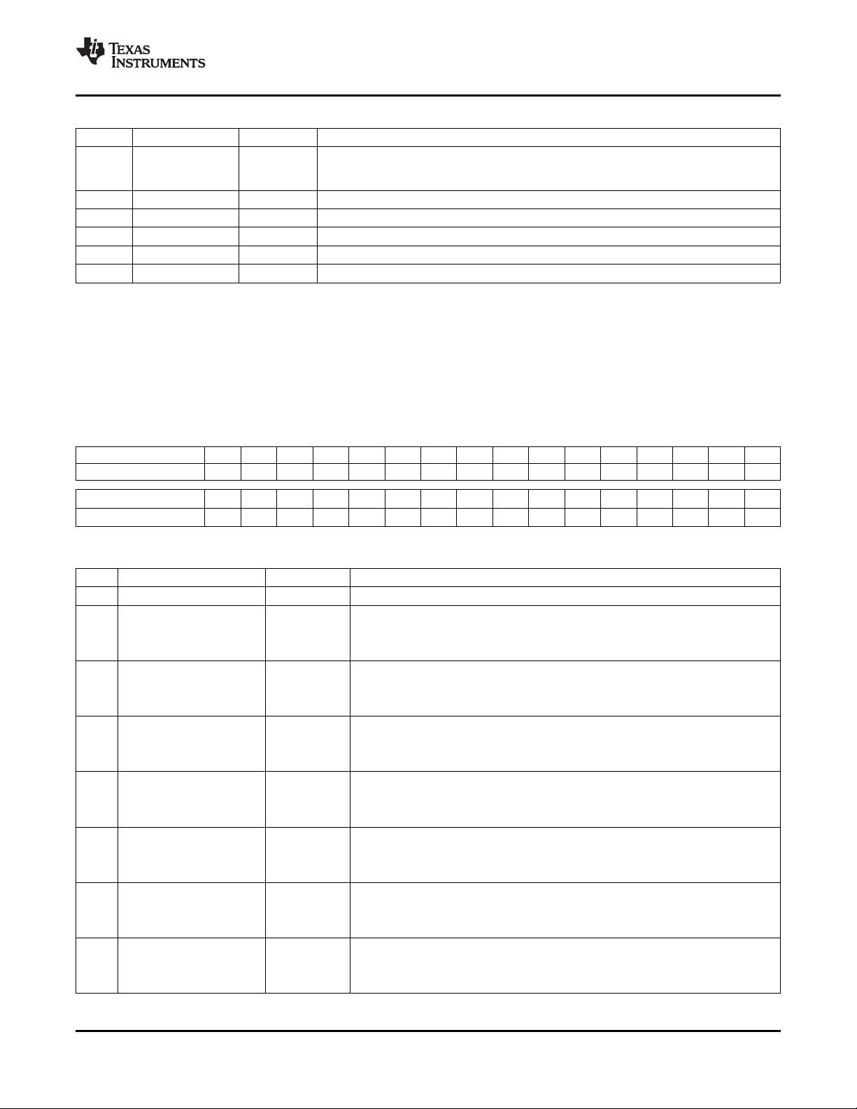
www.ti.com
SLLS693E – MAY 2007 – REVISED APRIL 2009
Table 4-44. Uncorrectable Error Status Register (continued)
BIT FIELD NAME ACCESS DESCRIPTION
12 PSN_TLP rcuh been poisoned by setting the poison bit and has inverted the extended CRC attached to
11:6 RSVD r Reserved. Return zeros when read.
5 SD_ERROR rcuh Surprise down error. See Surprise Down ECN for a description of this error condition.
4 DLL_ERROR rcuh Data link protocol error. This bit is asserted if a data link layer protocol error is detected.
3:1 RSVD r Reserved. Return zeros when read.
0 Undefined r The value read from this bit is undefined.
Poisoned TLP. This bit is asserted when an outgoing packet (request or completion) has
the end of the packet.
4.2.79 Uncorrectable Error Mask Register
The Uncorrectable Error Mask register controls the reporting of individual errors as they occur. When a bit
is set to one, the error status bits are still affected, but the error is not logged and no error reporting
message is sent upstream.
PCI register offset: 108h
Register type: Read Only, Read/Write
Default value: 0000 0000h
BIT NUMBER 31 30 29 28 27 26 25 24 23 22 21 20 19 18 17 16
RESET STATE 0 0 0 0 0 0 0 0 0 0 0 0 0 0 0 0
XIO3130
BIT NUMBER 15 14 13 12 11 10 9 8 7 6 5 4 3 2 1 0
RESET STATE 0 0 0 0 0 0 0 0 0 0 0 0 0 0 0 0
Table 4-45. Uncorrectable Error Mask Register
BIT FIELD NAME ACCESS DESCRIPTION
31:21 RSVD r Reserved. Return zeros when read.
Unsupported Request error mask.
20 UR_ERROR_MASK rwh 0 - Error condition is unmasked.
1 - Error condition is masked.
Extended CRC error mask.
19 ECRC_ERROR_MASK rwh 0 - Error condition is unmasked.
1 - Error condition is masked.
Malformed TLP mask.
18 MAL_TLP_MASK rwh 0 - Error condition is unmasked.
1 - Error condition is masked.
Receiver Overflow mask.
17 RX_OVERFLOW_MASK rwh 0 - Error condition is unmasked.
1 - Error condition is masked.
Unexpected Completion mask.
16 UNXP_CPL_MASK rwh 0 - Error condition is unmasked.
1 - Error condition is masked.
Completer Abort mask.
15 CPL_ABORT_MASK rwh 0 - Error condition is unmasked.
1 - Error condition is masked.
Completion Timeout mask.
14 CPL_TIMEOUT_MASK rwh 0 - Error condition is unmasked.
1 - Error condition is masked.
Submit Documentation Feedback XIO3130 Configuration Register Space 81
Page 82

XIO3130
SLLS693E – MAY 2007 – REVISED APRIL 2009
Table 4-45. Uncorrectable Error Mask Register (continued)
BIT FIELD NAME ACCESS DESCRIPTION
Flow Control error mask.
13 FC_ERROR_MASK rwh 0 - Error condition is unmasked.
1 - Error condition is masked.
Poisoned TLP mask.
12 PSN_TLP_MASK rwh 0 - Error condition is unmasked.
1 - Error condition is masked.
11:6 RSVD r Reserved. Return zeros when read.
Surprise Down error mask.
5 SD_MASK rwh 0 - Error condition is unmasked.
1 - Error condition is masked.
Data Link Protocol error mask.
4 DLL_ERROR_MASK rwh 0 - Error condition is unmasked.
1 - Error condition is masked.
3:1 RSVD r Reserved. Return zeros when read.
0 Undefined r The value read from this bit is undefined.
4.2.80 Uncorrectable Error Severity Register
The Uncorrectable Error Severity register controls the reporting of individual errors as ERR_FATAL or
ERR_NONFATAL. When a bit is set, the corresponding error condition is identified as fatal. When a bit is
clear, the corresponding error condition is identified as nonfatal.
www.ti.com
PCI register offset: 10Ch
Register type: Read Only, Read/Write
Default value: 0003 2030h
BIT NUMBER 31 30 29 28 27 26 25 24 23 22 21 20 19 18 17 16
RESET STATE 0 0 0 0 0 0 0 0 0 0 0 0 0 1 1 0
BIT NUMBER 15 14 13 12 11 10 9 8 7 6 5 4 3 2 1 0
RESET STATE 0 0 1 0 0 0 0 0 0 0 1 1 0 0 0 0
Table 4-46. Uncorrectable Error Severity Register
BIT FIELD NAME ACCESS DESCRIPTION
31:21 RSVD r Reserved. Return zeros when read.
Unsupported Request error severity.
20 UR_ERROR_SEVR rwh 0 - Error condition is signaled using ERR_NONFATAL.
1 - Error condition is signaled using ERR_FATAL.
Extended CRC error severity.
19 ECRC_ERROR_SEVR rwh 0 - Error condition is signaled using ERR_NONFATAL.
1 - Error condition is signaled using ERR_FATAL.
Malformed TLP severity.
18 MAL_TLP_SEVR rwh 0 - Error condition is signaled using ERR_NONFATAL.
1 - Error condition is signaled using ERR_FATAL.
Receiver Overflow severity.
17 RX_OVERFLOW_SEVR rwh 0 - Error condition is signaled using ERR_NONFATAL.
1 - Error condition is signaled using ERR_FATAL.
XIO3130 Configuration Register Space82 Submit Documentation Feedback
Page 83

www.ti.com
Table 4-46. Uncorrectable Error Severity Register (continued)
BIT FIELD NAME ACCESS DESCRIPTION
Unexpected Completion severity.
16 UNXP_CPL_SEVR rwh 0 - Error condition is signaled using ERR_NONFATAL.
1 - Error condition is signaled using ERR_FATAL.
Completer Abort severity.
15 CPL_ABORT_SEVR rwh 0 - Error condition is signaled using ERR_NONFATAL.
1 - Error condition is signaled using ERR_FATAL.
Completion Timeout severity.
14 CPL_TIMEOUT_SEVR rwh 0 - Error condition is signaled using ERR_NONFATAL.
1 - Error condition is signaled using ERR_FATAL.
Flow Control error severity.
13 FC_ERROR_SEVR rwh 0 - Error condition is signaled using ERR_NONFATAL.
1 - Error condition is signaled using ERR_FATAL.
Poisoned TLP severity.
12 PSN_TLP_SEVR rwh 0 - Error condition is signaled using ERR_NONFATAL.
1 - Error condition is signaled using ERR_FATAL.
11:6 RSVD r Reserved. Return zeros when read.
Surprise Down error severity.
5 SD_ERROR_SEVR rwh 0 - Error condition is signaled using ERR_NONFATAL.
1 - Error condition is signaled using ERR_FATAL.
Data Link Protocol error severity.
4 DLL_ERROR_SEVR rwh 0 - Error condition is signaled using ERR_NONFATAL.
1 - Error condition is signaled using ERR_FATAL.
3:1 RSVD r Reserved. Return zeros when read.
0 Undefined r The value read from this bit is undefined.
XIO3130
SLLS693E – MAY 2007 – REVISED APRIL 2009
4.2.81 Correctable Error Status Register
The Correctable Error Status register reports the status of individual errors as they occur. Software may
clear these bits only by writing a 1 to the desired location.
PCI register offset: 110h
Register type: Read Only, Cleared by a Write of one
Default value: 0000 0000h
BIT NUMBER 31 30 29 28 27 26 25 24 23 22 21 20 19 18 17 16
RESET STATE 0 0 0 0 0 0 0 0 0 0 0 0 0 0 0 0
BIT NUMBER 15 14 13 12 11 10 9 8 7 6 5 4 3 2 1 0
RESET STATE 0 0 0 0 0 0 0 0 0 0 0 0 0 0 0 0
Table 4-47. Correctable Error Status Register
BIT FIELD NAME ACCESS DESCRIPTION
31:14 RSVD r Reserved. Return zeroes when read.
13 ANFES rcuh Advisory nonfatal error status.
12 REPLAY_TMOUT rcuh
11:9 RSVD r Reserved. Return zeroes when read.
8 REPLAY_ROLL rcuh
Replay timer timeout. This bit is asserted when the replay timer expires for a pending
request or completion that has not been acknowledged.
REPLAY_NUM rollover. This bit is asserted when the replay counter rolls over when a
pending request of completion has not been acknowledged.
Submit Documentation Feedback XIO3130 Configuration Register Space 83
Page 84

XIO3130
SLLS693E – MAY 2007 – REVISED APRIL 2009
Table 4-47. Correctable Error Status Register (continued)
BIT FIELD NAME ACCESS DESCRIPTION
7 BAD_DLLP rcuh
6 BAD_TLP rcuh
5:1 RSVD r Reserved. Return zeros when read.
0 RX_ERROR rcuh
4.2.82 Correctable Error Mask Register
The Correctable Error Mask register controls the reporting of individual errors as they occur. When a bit is
set to one, error status bits are still affected, but the error is not logged and no error reporting message is
sent upstream.
PCI register offset: 114h
Register type: Read Only, Read/Write
Default value: 0000 2000h
BIT NUMBER 31 30 29 28 27 26 25 24 23 22 21 20 19 18 17 16
RESET STATE 0 0 0 0 0 0 0 0 0 0 0 0 0 0 0 0
BIT NUMBER 15 14 13 12 11 10 9 8 7 6 5 4 3 2 1 0
RESET STATE 0 0 1 0 0 0 0 0 0 0 0 0 0 0 0 0
Bad DLLP error. This bit is asserted when an 8b/10n error is detected by the PHY during
reception of a DLLP.
Bad TLP error. This bit is asserted when an 8b/10b error is detected by the PHY during
reception of a TLP.
Receiver error. This bit is asserted when an 8b/10b error is detected by the PHY at any
time.
www.ti.com
Table 4-48. Correctable Error Mask Register
BIT FIELD NAME ACCESS DESCRIPTION
31:14 RSVD r Reserved. Return zeros when read.
Advisory nonfatal error mask. This bit is set by default to enable compatibility with
13 ANFEM rwh
12 REPLAY_TMOUT_MASK rwh 0 – Error condition is unmasked
11:9 RSVD r Reserved. Return zeros when read.
8 REPLAY_ROLL_MASK rwh 0 – Error condition is unmasked
7 BAD_DLLP_MASK rwh 0 – Error condition is unmasked
6 BAD_TLP_MASK rwh 0 – Error condition is unmasked
5:1 RSVD r Reserved. Return zeros when read.
0 RX_ERROR_MASK rwh 0 – Error condition is unmasked
software that does not comprehend role-based error reporting.
0 – Error condition is unmasked
1 – Error condition is masked
Replay timer timeout mask.
1 – Error condition is masked
REPLAY_NUM rollover mask.
1 – Error condition is masked
Bad DLLP error mask.
1 – Error condition is masked
Bad TLP error mask.
1 – Error condition is masked
Receiver error mask.
1 – Error condition is masked
XIO3130 Configuration Register Space84 Submit Documentation Feedback
Page 85

www.ti.com
SLLS693E – MAY 2007 – REVISED APRIL 2009
4.2.83 Advanced Error Capabilities and Control Register
The Advanced Error Capabilities and Control register allows the system to monitor and control the
advanced error reporting capabilities.
PCI register offset: 118h
Register type: Read Only, Read/Write
Default value: 0000 00A0h
BIT NUMBER 31 30 29 28 27 26 25 24 23 22 21 20 19 18 17 16
RESET STATE 0 0 0 0 0 0 0 0 0 0 0 0 0 0 0 0
BIT NUMBER 15 14 13 12 11 10 9 8 7 6 5 4 3 2 1 0
RESET STATE 0 0 0 0 0 0 0 0 1 0 1 0 0 0 0 0
Table 4-49. Advanced Error Capabilities and Control Register
BIT FIELD NAME ACCESS DESCRIPTION
31:9 RSVD r Reserved. Return zeros when read.
Extended CRC check enable.
8 ECRC_CHK_EN rwh 0 – Extended CRC checking is disabled
1 – Extended CRC checking is enabled
7 ECRC_CHK_CAPABLE r
6 ECRC_GEN_EN rwh 0 – Extended CRC generation is disabled
5 ECRC_GEN_CAPABLE r
4:0 FIRST_ERR rh Error Status register corresponding to the class of the first error condition that was
Extended CRC check capable. This read-only bit returns a value of ‘1’ indicating that
the bridge is capable of checking extended CRC information.
Extended CRC generation enable.
1 – Extended CRC generation is enabled
Extended CRC generation capable. This read-only bit returns a value of ‘1’
indicating that the bridge is capable of generating extended CRC information.
First error pointer. This five-bit value reflects the bit position within the Uncorrectable
detected.
XIO3130
4.2.84 Header Log Register
The Header Log register stores the TLP header for the packet that lead to the most recently detected error
condition. Offset 11Ch contains the first DWORD. Offset 128h contains the last DWORD (in the case of a
4DW TLP header).
PCI register offset: 11Ch – 128h
Register type: Read only
Default value: 0000 0000h
BIT NUMBER 31 30 29 28 27 26 25 24 23 22 21 20 19 18 17 16
RESET STATE 0 0 0 0 0 0 0 0 0 0 0 0 0 0 0 0
BIT NUMBER 15 14 13 12 11 10 9 8 7 6 5 4 3 2 1 0
RESET STATE 0 0 0 0 0 0 0 0 0 0 0 0 0 0 0 0
Submit Documentation Feedback XIO3130 Configuration Register Space 85
Page 86

XIO3130
SLLS693E – MAY 2007 – REVISED APRIL 2009
4.3 PCI Express Downstream Port Registers
The default reset domain for all downstream port registers is SBRST. Some register fields are placed in a
different reset domain from the default reset domain; all bit and field descriptions identify any unique reset
domains. Generally, all sticky bits are placed in the GRST domain and all (non-sticky) EEPROM loadable
bits are placed in the PERST domain.
4.3.1 PCI Configuration Space (Downstream Port) Register Map
Table 4-50. PCI Express Downstream Port Configuration Register Map (Type 1)
Register Name Offset
Device ID Vendor ID 000h
Status Command 004h
Class Code Revision ID 008h
BIST Header Type Latency Timer Cache Line Size 00Ch
Reserved 010h-014h
Secondary Latency Timer Subordinate Bus Number Secondary Bus Number Primary Bus Number 018h
Secondary Status I/O Limit I/O Base 01Ch
Memory Limit Memory Base 020h
Pre-fetchable Memory Limit Pre-fetchable Memory Base 024h
Pre-fetchable Base Upper 32 Bits 028h
Pre-fetchable Limit Upper 32 Bits 02Ch
I/O Limit Upper 16 Bits I/O Base Upper 16 Bits 030h
Reserved Capabilities Pointer 034h
Reserved 038h
Bridge Control Interrupt Pin Interrupt Line 03Ch
Reserved 040h-04Ch
Power Management Capabilities Next-item Pointer PM CAP ID 050h
PM Data (RSVD) PMCSR_BSE Power Management CSR 054h
Reserved 058h-06Ch
MSI Message Control Next-item Pointer MSI CAP ID 070h
MSI Message Address 074h
MSI Upper Message Address 078h
Reserved MSI Message Data 07Ch
Reserved Next-item Pointer SSID/SSVID CAP ID 080h
Subsystem ID Subsystem Vendor ID 084h
Reserved 088h-08Ch
PCI Express Capabilities Register Next-item Pointer PCI Express Capability ID 090h
Device Capabilities 094h
Device Status Device Control 098h
Link Capabilities 09Ch
Link Status Link Control 0A0h
Slot Capabilities A4h
Slot Status Slot Control A8h
Reserved 0ACh-0C4h
TI Proprietary 0C8h-0D0h
General Control 0D4h
Reserved 0D8h-0E8h
General Slot Info Reserved LOs Idle Timeout 0ECh
Reserved 0F0h-0FCh
www.ti.com
XIO3130 Configuration Register Space86 Submit Documentation Feedback
Page 87

www.ti.com
SLLS693E – MAY 2007 – REVISED APRIL 2009
Table 4-51. Extended Configuration Space (Downstream Port)
Register Name Offset
Next Capability Offset / Capability Version PCI Express Advanced Error Reporting Capabilities ID 100h
Uncorrectable Error Status Register 104h
Uncorrectable Error Mask Register 108h
Uncorrectable Error Severity Register 10Ch
Correctable Error Status Register 110h
Correctable Error Mask 114h
Advanced Error Capabilities and Control 118h
Header Log Register 11Ch
Header Log Register 120h
Header Log Register 124h
Header Log Register 128h
Reserved 12Ch-FFCh
4.3.2 Vendor ID Register
This 16-bit read-only register contains the value 104Ch, which is the vendor ID assigned to Texas
Instruments.
XIO3130
PCI register offset: 00h
Register type: Read only
Default value: 104Ch
BIT NUMBER 15 14 13 12 11 10 9 8 7 6 5 4 3 2 1 0
RESET STATE 0 0 0 1 0 0 0 0 0 1 0 0 1 1 0 0
4.3.3 Device ID Register
This 16-bit read-only register contains the device ID assigned by TI to the XIO3130. The value in this
register is the same for all downstream ports, as defined in the following table.
PCI register offset: 02h
Register type: Read only
Default value: 8233h
BIT NUMBER 15 14 13 12 11 10 9 8 7 6 5 4 3 2 1 0
RESET STATE 1 0 0 0 0 0 1 0 0 0 1 1 0 0 1 1
4.3.4 Command Register
The Command register controls the way the downstream port bridge behaves on its primary interface; i.e.,
the internal PCI bus between the upstream and downstream ports.
PCI register offset: 04h
Register type: Read/Write; Read Only
Default value: 0000h
BIT NUMBER 15 14 13 12 11 10 9 8 7 6 5 4 3 2 1 0
RESET STATE 0 0 0 0 0 0 0 0 0 0 0 0 0 0 0 0
Submit Documentation Feedback XIO3130 Configuration Register Space 87
Page 88

XIO3130
SLLS693E – MAY 2007 – REVISED APRIL 2009
Table 4-52. Bit Descriptions – Command Register
BIT FIELD NAME ACCESS DESCRIPTION
15:11 RSVD r Reserved. When read, these bits return zeros.
INTx disable. This bit is used to enable device-specific INTx interrupts. The XIO3130
10 INT_DISABLE rw
9 FBB_ENB r Fast back-to-back enable. This bit does not apply to PCI-Express, so it returns zero when read.
8 SERR_ENB rw
7 STEP_ENB r Address/data stepping control. This bit does not apply to PCI-Express and is hardwired to 0.
6 PERR_ENB rw
5 VGA_ENB r
4 MWI_ENB r
3 SPECIAL r Special cycle enable. This bit does not apply to PCI-Express and is hardwired to zero.
2 MASTER_ENB rw
1 MEMORY_ENB rw
0 IO_ENB rw I/O space enable. Setting this bit enables the downstream port to respond to I/O transactions.
downstream ports can generate INTx interrupts due to PCI Hot Plug events. The XIO3130
forwards INTx messages from downstream ports to the upstream port (see INTx Support
section) regardless of this bit.
SERR enable. The relevant error checking is unnecessary for the XIO3130 internal PCI bus.
When set, this bit enables the transmission by the primary interface of ERR_NONFATAL and
ERR_FATAL messages forwarded from the secondary interface. This bit does not affect
transmission of ERR_COR messages.
Parity error response enable. This bit has no impact on hardware behavior. It is assumed that
the relevant error checking is unnecessary for the XIO3130 internal PCI bus.
VGA palette snoop enable. The XIO3130 does not support VGA palette snooping, so this bit
returns zero when read.
Memory write and invalidate enable. This bit does not apply to PCI-Express, so it is hardwired to
zero.
Bus master enable. When set, the XIO3130 is enabled to initiate cycles on the downstream PCI
Express interface.
0 – Downstream PCI Express interface cannot initiate transactions. The XIO3130 must
disable response to memory and I/O transactions on the downstream interface.
1 – Downstream PCI Express interface can initiate transactions. The bridge can forward
memory and I/O transactions.
Memory response enable. Setting this bit enables the downstream port to respond to memory
transactions.
www.ti.com
4.3.5 Status Register
The Status register provides information about the downstream port’s primary interface, i.e., the internal
PCI bus between the upstream and downstream ports.
PCI register offset: 06h
Register type: Read Only; Clear by a Write of One; Hardware Update
Default value: 0010h
BIT NUMBER 15 14 13 12 11 10 9 8 7 6 5 4 3 2 1 0
RESET STATE 0 0 0 0 0 0 0 0 0 0 0 0 0 0 0 0
Table 4-53. Bit Descriptions – Status Register
BIT FIELD NAME ACCESS DESCRIPTION
Detected parity error. This bit is set when the virtual internal PCI interface receives a
poisoned TLP. This bit is set regardless of the state of the Parity Error Response bit in the
15 PAR_ERR rcu
14 SYS_ERR rcu
13 MABORT r
Command register.
0 – No parity error detected.
1 – Parity error detected.
Signaled system error. This bit is set when the XIO3130 sends an ERR_FATAL or
ERR_NONFATAL message upstream and the SERR Enable bit in the Command register is
set.
0 – No error signaled.
1 – ERR_FATAL or ERR_NONFATAL signaled.
Received master abort. This bit is hardwired to zero. It is assumed that the relevant error
checking is unnecessary for the XIO3130 internal PCI bus.
XIO3130 Configuration Register Space88 Submit Documentation Feedback
Page 89

www.ti.com
SLLS693E – MAY 2007 – REVISED APRIL 2009
Table 4-53. Bit Descriptions – Status Register (continued)
BIT FIELD NAME ACCESS DESCRIPTION
12 TABORT_REC r
11 TABORT_SIG r
10:9 PCI_SPEED r DEVSEL timing. These bits are read only zero because they do not apply to PCI Express.
8 DATAPAR rcu completion or poisons a write request on the internal virtual PCI bus. This bit is never set if
7 FBB_CAP r
6 RSVD r Reserved. When read, this bit returns zero.
5 66MHZ r
4 CAPLIST r
3 INT_STATUS r
2:0 RSVD r Reserved. When read, these bits return zeros.
Received target abort. This bit is hardwired to zero. It is assumed that the relevant error
checking is unnecessary for the XIO3130 internal PCI bus.
Signaled target abort. This bit is hardwired to zero. It is assumed that the relevant error
checking is unnecessary for the XIO3130 internal PCI bus.
Master data parity error. This bit is set when the downstream port receives a poisoned
the parity error response enable bit in the Command register is clear.
Fast back-to-back capable. This bit does not have a meaningful context for a PCI Express
device and is hardwired to zero.
66-MHz capable. This bit does not have a meaningful context for a PCI Express device and is
hardwired to zero.
Capabilities list. This bit returns 1 when read, indicating that the XIO3130 supports additional
PCI capabilities.
Interrupt status. This bit reflects the INTx interrupt status of the function. The XIO3130
forwards INTx messages from downstream ports to the upstream port.
4.3.6 Class Code and Revision ID Register
XIO3130
This read-only register categorizes the Base Class, Sub Class, and Programming Interface of the
XIO3130. The Base Class is 06h, which identifies the device as a bridge device. The Sub Class is 04h,
which identifies the function as a PCI-to-PCI bridge. The Programming Interface is 00h. In addition, the TI
chip revision is indicated in the lower byte (01h).
PCI register offset: 08h
Register type: Read only
Default value: 0604 0001h
BIT NUMBER 31 30 29 28 27 26 25 24 23 22 21 20 19 18 17 16
RESET STATE 0 0 0 0 0 1 1 0 0 0 0 0 0 1 0 0
BIT NUMBER 15 14 13 12 11 10 9 8 7 6 5 4 3 2 1 0
RESET STATE 0 0 0 0 0 0 0 0 0 0 0 0 0 0 0 1
Table 4-54. Bit Descriptions – Class Code and Revision ID Register
BIT FIELD NAME ACCESS DESCRIPTION
31:24 BASECLASS r
23:16 SUBCLASS r
15:8 PGMIF r Programming interface. This field returns 00h when read.
7:0 CHIPREV r Silicon revision. This field returns the silicon revision.
Base class. This field returns 06h when read, which classifies the function as a bridge
device.
Subclass. This field returns 04h when read, which specifically classifies the function as a
PCI-to-PCI bridge.
Submit Documentation Feedback XIO3130 Configuration Register Space 89
Page 90

XIO3130
SLLS693E – MAY 2007 – REVISED APRIL 2009
4.3.7 Cache Line Size Register
The Cache Line Size register is implemented by PCI Express devices as a read-write field for legacy
compatibility, but has no impact on any PCI Express device functionality.
PCI register offset: 0Ch
Register type: Read/Write
Default value: 00h
BIT NUMBER 7 6 5 4 3 2 1 0
RESET STATE 0 0 0 0 0 0 0 0
4.3.8 Primary Latency Timer Register
This read-only register has no meaningful context for a PCI Express device, so it returns zeros when read.
PCI register offset: 0Dh
Register type: Read only
Default value: 00h
BIT NUMBER 7 6 5 4 3 2 1 0
RESET STATE 0 0 0 0 0 0 0 0
4.3.9 Header Type Register
www.ti.com
This read-only register indicates that this function has a Type 1 PCI header. Bit seven of this register is
zero, indicating that the XIO3130 downstream port PCI-to-PCI bridge is not a multifunction device.
PCI register offset: 0Eh
Register type: Read only
Default value: 01h
BIT NUMBER 7 6 5 4 3 2 1 0
RESET STATE 0 0 0 0 0 0 0 1
4.3.10 BIST Register
Since the XIO3130 does not support a built-in self test (BIST), this read-only register returns the value 00h
when read.
PCI register offset: 0Fh
Register type: Read only
Default value: 00h
BIT NUMBER 7 6 5 4 3 2 1 0
RESET STATE 0 0 0 0 0 0 0 0
90 XIO3130 Configuration Register Space Submit Documentation Feedback
Page 91

www.ti.com
4.3.11 Primary Bus Number
This register specifies the bus number of the PCI bus segment for the downstream port primary interface
(i.e., the internal PCI bus).
PCI register offset: 18h
Register type: Read/Write
Default value: 00h
BIT NUMBER 7 6 5 4 3 2 1 0
RESET STATE 0 0 0 0 0 0 0 0
4.3.12 Secondary Bus Number
This register specifies the bus number of the PCI bus segment for the downstream port secondary
interface (i.e., the PCI Express interface). The XIO3130 uses this register to determine how to respond to
a Type 1 configuration transaction.
PCI register offset: 19h
Register type: Read/Write
Default value: 00h
BIT NUMBER 7 6 5 4 3 2 1 0
RESET STATE 0 0 0 0 0 0 0 0
XIO3130
SLLS693E – MAY 2007 – REVISED APRIL 2009
4.3.13 Subordinate Bus Number
This register specifies the bus number of the highest number PCI bus segment that is downstream of the
XIO3130 downstream port. The XIO3130 uses this register to determine how to respond to a Type 1
configuration transaction.
PCI register offset: 1Ah
Register type: Read/Write
Default value: 00h
BIT NUMBER 7 6 5 4 3 2 1 0
RESET STATE 0 0 0 0 0 0 0 0
4.3.14 Secondary Latency Timer Register
This register does not apply to PCI-Express, so it is hardwired to zero.
PCI register offset: 1Bh
Register type: Read only
Default value: 00h
BIT NUMBER 7 6 5 4 3 2 1 0
RESET STATE 0 0 0 0 0 0 0 0
Submit Documentation Feedback XIO3130 Configuration Register Space 91
Page 92

XIO3130
SLLS693E – MAY 2007 – REVISED APRIL 2009
4.3.15 I/O Base Register
This read/write register specifies the lower limit of the I/O addresses that the XIO3130 downstream port
forwards downstream.
PCI register offset: 1Ch
Register type: Read/Write; Read Only
Default value: 01h
BIT NUMBER 7 6 5 4 3 2 1 0
RESET STATE 0 0 0 0 0 0 0 1
Table 4-55. Bit Descriptions – I/O Base Register
BIT FIELD NAME ACCESS DESCRIPTION
I/O base. This field defines the bottom address of the I/O address range that is used to
determine when to forward I/O transactions from one interface to the other. These bits
7:4 IOBASE rw correspond to address bits [15:12] in the I/O address. The lower 12 bits are assumed to be 0.
The 16 bits that correspond to address bits [31:16] of the I/O address are defined in the I/O
Base Upper 16 Bits register.
3:0 IOTYPE r I/O type. This field is read-only 01h, which indicates 32 bit I/O addressing support.
4.3.16 I/O Limit Register
This read/write register specifies the upper limit of the I/O addresses that the XIO3130 downstream port
forwards downstream.
www.ti.com
PCI register offset: 1Dh
Register type: Read/Write; Read Only
Default value: 01h
BIT NUMBER 7 6 5 4 3 2 1 0
RESET STATE 0 0 0 0 0 0 0 1
Table 4-56. Bit Descriptions – I/O Limit Register
BIT FIELD NAME ACCESS DESCRIPTION
I/O limit. This field defines the top address of the I/O address range that is used to determine
7:4 IOLIMIT rw address bits [15:12] in the I/O address. The lower 12 bits are assumed to be FFFh. The 16
3:0 IOTYPE r I/O type. This field is read-only 01h, which indicates 32-bit I/O addressing support.
when to forward I/O transactions from one interface to the other. These bits correspond to
bits that correspond to address bits [31:16] of the I/O address are defined in the I/O Limit
Upper 16 Bits register.
4.3.17 Secondary Status Register
The Secondary Status register provides information about the downstream port PCI Express interface.
PCI register offset: 1Eh
Register type: Read Only; Clear by a Write of One; Hardware Update
Default value: 0000h
BIT NUMBER 15 14 13 12 11 10 9 8 7 6 5 4 3 2 1 0
RESET STATE 0 0 0 0 0 0 0 0 0 0 0 0 0 0 0 0
92 XIO3130 Configuration Register Space Submit Documentation Feedback
Page 93

www.ti.com
SLLS693E – MAY 2007 – REVISED APRIL 2009
Table 4-57. Bit Descriptions – Secondary Status Register
BIT FIELD NAME ACCESS DESCRIPTION
Detected parity error. This bit is set when the PCI Express interface receives a poisoned TLP
on the downstream port. This bit is set regardless of the state of the Parity Error Response bit
15 PAR_ERR rcu
14 SYS_ERR rcu
13 MABORT rcu
12 TABORT_REC rcu
11 TABORT_SIG rcu
10:9 PCI_SPEED r DEVSEL timing. These bits are hardwired to 00. These bits do not apply to PCI Express.
8 DATAPAR rcu poisons a write request on the downstream PCI Express interface. This bit is never set if the
7 FBB_CAP r Fast back-to-back capable. This bit is hardwired to zero. This bit does not apply to PCI Express.
6 RSVD r Reserved. When read, this bit returns zero.
5 66MHZ r 66-MHz capable. This bit is hardwired to zero. This bit does not apply to PCI Express.
4:0 RSVD r Reserved. When read, these bits return zeros.
in the Bridge Control register.
0 – No parity error detected.
1 – Parity error detected.
Received System Error. This bit is set when the XIO3130 sends an ERR_FATAL or
ERR_NONFATAL message upstream and the SERR Enable bit in the Command register is set.
0 – No error signaled.
1 – ERR_FATAL or ERR_NONFATAL signaled.
Received master abort. This bit is set when the downstream PCI Express interface of the
XIO3130 receives a completion with Unsupported Request Status.
0 – Unsupported Request not received.
1 – Unsupported Request received on.
Received target abort. This bit is set when the downstream PCI Express interface of the
XIO3130 receives a completion with Completer Abort Status.
0 – Completer Abort not received.
1 - Completer Abort received.
Signaled target abort. This bit is set when the downstream PCI Express interface completes a
Request with Completer Abort Status.
0 – Completer Abort not signaled.
1 – Completer Abort signaled.
Master data parity error. This bit is set when the XIO3130 receives a poisoned completion or
parity error response enable bit in the Bridge Control register is clear.
XIO3130
4.3.18 Memory Base Register
This read/write register specifies the lower limit of the memory addresses that the downstream port
forwards downstream.
PCI register offset: 20h
Register type: Read/Write; Read Only
Default value: 0000h
BIT NUMBER 15 14 13 12 11 10 9 8 7 6 5 4 3 2 1 0
RESET STATE 0 0 0 0 0 0 0 0 0 0 0 0 0 0 0 0
Table 4-58. IBit Descriptions – Memory Base Register
BIT FIELD NAME ACCESS DESCRIPTION
Memory base. This field defines the bottom address of the memory address range that is
15:4 MEMBASE rw
3:0 RSVD r Reserved. When read, these bits return zeros.
Submit Documentation Feedback XIO3130 Configuration Register Space 93
used to determine when to forward memory transactions from one interface to the other.
These bits correspond to address bits [31:20] in the memory address. The lower 20 bits are
assumed to be zero.
Page 94

XIO3130
SLLS693E – MAY 2007 – REVISED APRIL 2009
4.3.19 Memory Limit Register
This read/write register specifies the upper limit of the memory addresses that the downstream port
forwards downstream.
PCI register offset: 22h
Register type: Read/Write; Read Only
Default value: 0000h
BIT NUMBER 15 14 13 12 11 10 9 8 7 6 5 4 3 2 1 0
RESET STATE 0 0 0 0 0 0 0 0 0 0 0 0 0 0 0 0
Table 4-59. Bit Descriptions – Memory Limit Register
BIT FIELD NAME ACCESS DESCRIPTION
Memory limit. This field defines the top address of the memory address range that is used to
15:4 MEMLIMIT rw
3:0 RSVD r Reserved. When read, these bits return zeros.
4.3.20 Pre-fetchable Memory Base Register
This read/write register specifies the lower limit of the pre-fetchable memory addresses that the
downstream port forwards downstream.
determine when to forward memory transactions from one interface to the other. These bits
correspond to address bits [31:20] in the memory address. The lower 20 bits are assumed to
be FFFFFh.
www.ti.com
PCI register offset: 24h
Register type: Read/Write; Read Only
Default value: 0001h
BIT NUMBER 15 14 13 12 11 10 9 8 7 6 5 4 3 2 1 0
RESET STATE 0 0 0 0 0 0 0 0 0 0 0 0 0 0 0 1
Table 4-60. Descriptions – Pre-fetchable Memory Base Register
BIT FIELD NAME ACCESS DESCRIPTION
Pre-fetchable memory base. This field defines the bottom address of the pre-fetchable
15:4 PREBASE rw one interface to the other. These bits correspond to address bits [31:20] in the memory
3:0 64BIT r
memory address range that is used to determine when to forward memory transactions from
address. The lower 20 bits are assumed to be zero. The Pre-fetchable Base Upper 32 Bits
register is used to specify the bit [63:32] of the 64-bit pre-fetchable memory address.
64-bit memory indicator. These read-only bits indicate that 64-bit addressing is supported for
this memory window.
4.3.21 Pre-fetchable Memory Limit Register
This read/write register specifies the upper limit of the pre-fetchable memory addresses that the
downstream port forwards downstream.
PCI register offset: 26h
Register type: Read/Write; Read Only
Default value: 0001h
BIT NUMBER 15 14 13 12 11 10 9 8 7 6 5 4 3 2 1 0
RESET STATE 0 0 0 0 0 0 0 0 0 0 0 0 0 0 0 1
94 XIO3130 Configuration Register Space Submit Documentation Feedback
Page 95

www.ti.com
SLLS693E – MAY 2007 – REVISED APRIL 2009
Table 4-61. Bit Descriptions – Pre-fetchable Memory Limit Register
BIT FIELD NAME ACCESS DESCRIPTION
Pre-fetchable memory limit. This field defines the top address of the pre-fetchable memory
15:4 PRELIMIT rw interface to the other. These bits correspond to address bits [31:20] in the memory address.
3:0 64BIT r
address range that is used to determine when to forward memory transactions from one
The lower 20 bits are assumed to be FFFFFh. The Pre-fetchable Limit Upper 32 Bits register
is used to specify the bit [63:32] of the 64-bit pre-fetchable memory address.
64-bit memory indicator. These read-only bits indicate that 64-bit addressing is supported for
this memory window.
4.3.22 Pre-fetchable Base Upper 32 Bits Register
This read/write register specifies the upper 32 bits of the Pre-fetchable Memory Base register.
PCI register offset: 28h
Register type: Read/Write
Default value: 0000 0000h
BIT NUMBER 31 30 29 28 27 26 25 24 23 22 21 20 19 18 17 16
RESET STATE 0 0 0 0 0 0 0 0 0 0 0 0 0 0 0 0
BIT NUMBER 15 14 13 12 11 10 9 8 7 6 5 4 3 2 1 0
RESET STATE 0 0 0 0 0 0 0 0 0 0 0 0 0 0 0 0
XIO3130
Table 4-62. Bit Descriptions – Pre-fetchable Base Upper 32 Bits Register
BIT FIELD NAME ACCESS DESCRIPTION
31:0 PREBASE rw address of the pre-fetchable memory address range that is used to determine when to forward
Pre-fetchable memory base upper 32 bits. This field defines the upper 32 bits of the bottom
memory transactions downstream.
4.3.23 Pre-fetchable Limit Upper 32 Bits Register
This read/write register specifies the upper 32 bits of the Pre-fetchable Memory Limit register.
PCI register offset: 2Ch
Register type: Read/Write
Default value: 0000 0000h
BIT NUMBER 31 30 29 28 27 26 25 24 23 22 21 20 19 18 17 16
RESET STATE 0 0 0 0 0 0 0 0 0 0 0 0 0 0 0 0
BIT NUMBER 15 14 13 12 11 10 9 8 7 6 5 4 3 2 1 0
RESET STATE 0 0 0 0 0 0 0 0 0 0 0 0 0 0 0 0
Table 4-63. Descriptions – Pre-fetchable Limit Upper 32 Bits Register
BIT FIELD NAME ACCESS DESCRIPTION
31:0 PRELIMIT rw of the pre-fetchable memory address range that is used to determine when to forward memory
Pre-fetchable memory limit upper 32 bits. This field defines the upper 32 bits of the top address
transactions downstream.
Submit Documentation Feedback XIO3130 Configuration Register Space 95
Page 96

XIO3130
SLLS693E – MAY 2007 – REVISED APRIL 2009
4.3.24 I/O Base Upper 16 Bits Register
This read/write register specifies the upper 16 bits of the I/O Base register.
PCI register offset: 30h
Register type: Read/Write
Default value: 0000h
BIT NUMBER 15 14 13 12 11 10 9 8 7 6 5 4 3 2 1 0
RESET STATE 0 0 0 0 0 0 0 0 0 0 0 0 0 0 0 0
Table 4-64. Bit Descriptions – I/O Base Upper 16 Bits Register
BIT FIELD NAME ACCESS DESCRIPTION
15:0 IOBASE rw
4.3.25 I/O Limit Upper 16 Bits Register
This read/write register specifies the upper 16 bits of the I/O Limit register.
PCI register offset: 32h
Register type: Read/Write
Default value: 0000h
BIT NUMBER 15 14 13 12 11 10 9 8 7 6 5 4 3 2 1 0
RESET STATE 0 0 0 0 0 0 0 0 0 0 0 0 0 0 0 0
I/O base upper 16 bits. This field defines the upper 16 bits of the bottom address of the I/O
address range that is used to determine when to forward I/O transactions downstream.
www.ti.com
Table 4-65. Bit Descriptions – I/O Limit Upper 16 Bits Register
BIT FIELD NAME ACCESS DESCRIPTION
15:0 IOLIMIT rw
I/O limit upper 16 bits. This field defines the upper 16 bits of the top address of the I/O
address range that is used to determine when to forward I/O transactions downstream.
4.3.26 Capabilities Pointer Register
This read-only register provides a pointer into the PCI configuration header, which is where the PCI power
management block resides. Since the PCI power management registers begin at 50h, this register is
hardwired to 50h.
PCI register offset: 34h
Register type: Read only
Default value: 50h
BIT NUMBER 7 6 5 4 3 2 1 0
RESET STATE 0 1 0 1 0 0 0 0
96 XIO3130 Configuration Register Space Submit Documentation Feedback
Page 97

www.ti.com
4.3.27 Interrupt Line Register
This read/write register, which the system programs, indicates to the software which interrupt line that the
XIO3130 downstream port has assigned to it. The default value of this register is FFh, which indicates that
an interrupt line has not yet been assigned to the function. This register is essentially a scratch-pad
register; it has no effect on the XIO3130 itself.
PCI register offset: 3Ch
Register type: Read/Write
Default value: FFh
BIT NUMBER 7 6 5 4 3 2 1 0
RESET STATE 1 1 1 1 1 1 1 1
4.3.28 Interrupt Pin Register
The Interrupt Pin register is read-only, which indicates that the XIO3130 downstream ports generate INTx
interrupts as follows:
• Downstream port 0 on PCI Interrupt pin INTA (register value of 01h)
• Downstream port 1 on PCI Interrupt pin INTA (register value of 01h)
• Downstream port 2 on PCI Interrupt pin INTA (register value of 01h)
Interrupts originated by XIO3130 downstream ports are associated with the primary side of the
downstream port PCI-to-PCI bridge, and as a result are only passed through the upstream port PCI-to-PCI
bridge as described in PCI Express Base Specification Revision 1.1, Page 69, Table 2-13.
XIO3130
SLLS693E – MAY 2007 – REVISED APRIL 2009
PCI register offset: 3Dh
Register type: Read only
Default value: 01h
BIT NUMBER 7 6 5 4 3 2 1 0
RESET STATE 0 0 0 0 0 0 0 1
4.3.29 Bridge Control Register
The Bridge Control register provides extensions to the Command register that are specific to a bridge.
PCI register offset: 3Eh
Register type: Read/Write; Read Only
Default value: 0000h
BIT NUMBER 15 14 13 12 11 10 9 8 7 6 5 4 3 2 1 0
RESET STATE 0 0 0 0 0 0 0 0 0 0 0 0 0 0 0 0
Table 4-66. Bit Descriptions – Bridge Control Register
BIT FIELD NAME ACCESS DESCRIPTION
15:12 RSVD r Reserved. When read, these bits return zeros.
11 DTSERR r Discard timer SERR enable. This bit is hardwired to zero. This bit does not apply to PCI Express.
10 DTSTATUS r Discard timer status. This bit is hardwired to zero. This bit does not apply to PCI Express.
9 SEC_DT r Secondary discard timer. This bit is hardwired to zero. This bit does not apply to PCI Express.
8 PRI_DEC r Primary discard timer. This bit is hardwired to zero. This bit does not apply to PCI Express.
7 FBB_EN r Fast back-to-back enable. This bit is hardwired to zero. This bit does not apply to PCI Express.
Submit Documentation Feedback XIO3130 Configuration Register Space 97
Page 98

XIO3130
SLLS693E – MAY 2007 – REVISED APRIL 2009
Table 4-66. Bit Descriptions – Bridge Control Register (continued)
BIT FIELD NAME ACCESS DESCRIPTION
Secondary bus reset. This bit is set when the software resets all devices downstream of the
XIO3130 downstream port. Setting this bit causes the downstream port to send a reset downstream
6 SRST rw
5 MAM r Master abort mode. This bit is hardwired to zero. This bit does not apply to PCI Express.
4 VGA16 rw
3 VGA rw
2 ISA rw
1 SERR_EN rw
0 PERR_EN rw
via a training sequence.
0 – Downstream port not in Reset state
1 – Downstream port in Reset state
VGA 16-bit decode. This bit enables the XIO3130 downstream port to provide full 16-bit decoding
for VGA I/O addresses. This bit only has meaning if the VGA enable bit is set.
0 – Ignore address bits [15:10] when decoding VGA I/O addresses.
1 – Decode address bits [15:10] when decoding VGA I/O addresses.
VGA enable. This bit modifies the response by the XIO3130 downstream port to VGA-compatible
addresses. If this bit is set, the XIO3130 downstream port positively decodes and forwards the
following accesses on the primary interface to the secondary interface (and, conversely, blocks the
forwarding of these addresses from the secondary to primary interface):
• = Memory accesses in the range 000A 0000h to 000BFFFFh
• = I/O addresses in the first 64KB of the I/O address space (address bits [31:16] are 0000h.) and
where address bits [9:0] are in the range 3B0h to 3BBh or 3C0h to 3DFh (inclusive of ISA
address aliases; address bits [15:10] may possess any value and are not used in the
decoding).
If the VGA Enable bit is set, forwarding of VGA addresses is independent of the value of the ISA
Enable bit (located in the Bridge Control register), the I/O address range and memory address
ranges defined by the I/O Base and Limit registers, the Memory Base and Limit registers, and the
Pre-fetchable Memory Base and Limit registers of the bridge. Forwarding of VGA addresses is
qualified by the I/O Enable and Memory Enable bits in the Command register.
0 – Do not forward VGA-compatible memory and I/O addresses from the primary to secondary
interface unless they are enabled for forwarding by the defined I/O and memory address
ranges.
1 – Forward VGA-compatible memory and I/O addresses from the primary interface to the
secondary interface (if the I/O Enable and Memory Enable bits are set) independent of the I/O
and memory address ranges and independent of the ISA Enable bit.
ISA enable. This bit modifies the response by the XIO3130 downstream port to ISA I/O addresses.
This bit applies only to I/O addresses that are enabled by the I/O Base and I/O Limit registers and
are in the first 64 KB of PCI I/O address space (0000 0000h to 0000 FFFFh). If this bit is set, the
bridge blocks any forwarding from primary to secondary of I/O transactions addressing the last 768
bytes in each 1 KB block. In the opposite direction (secondary to primary), I/O transactions are
forwarded if they address the last 768 bytes in each 1K block.
0 – Forward downstream all I/O addresses in the address range defined by the I/O Base and I/O
Limit registers.
1 – Forward upstream ISA I/O addresses in the address range defined by the I/O Base and I/O
Limit registers that are in the first 64 KB of PCI I/O address space (top 768 bytes of each 1 KB
block).
SERR enable. This bit controls the forwarding of system error events upstream from the secondary
interface to the primary interface. The XIO3130’s downstream port forwards system error events
upstream when:
• = This bit is set.
• = The SERR enable bit in the downstream port command register is set.
• = A nonfatal or fatal error condition is detected on the secondary interface (i.e., the PCI Express
interface).
0 – Disable the reporting of nonfatal errors and fatal errors.
1 – Enable the reporting of nonfatal errors and fatal errors.
Parity error response enable. For PCI Express, this bit controls responses to poisoned TLPs
received on the downstream port.
0 – Disable responses to poisoned TLPs.
1 – Enable responses to poisoned TLPs.
www.ti.com
XIO3130 Configuration Register Space98 Submit Documentation Feedback
Page 99

www.ti.com
4.3.30 Capability ID Register
This read-only register identifies the linked list item as the register for PCI power management. It returns
01h when read.
PCI register offset: 50h
Register type: Read only
Default value: 01h
BIT NUMBER 7 6 5 4 3 2 1 0
RESET STATE 0 0 0 0 0 0 0 1
4.3.31 Next-Item Pointer Register
The contents of this read-only register indicate the next item in the linked list of capabilities for the
XIO3130 downstream port. This register reads 70h, which points to the MSI Capabilities registers.
PCI register offset: 51h
Register type: Read only
Default value: 70h
BIT NUMBER 7 6 5 4 3 2 1 0
RESET STATE 0 1 1 1 0 0 0 0
XIO3130
SLLS693E – MAY 2007 – REVISED APRIL 2009
4.3.32 Power Management Capabilities Register
This register indicates the capabilities of the XIO3130 downstream port related to PCI power
management.
PCI register offset: 52h
Register type: Read only
Default value: XXX3h
BIT NUMBER 15 14 13 12 11 10 9 8 7 6 5 4 3 2 1 0
RESET STATE y 1 1 x 1 1 x 0 0 y 0 0 0 0 1 1
Table 4-67. Bit Descriptions – Power Management Capabilities Register
BIT FIELD NAME ACCESS DESCRIPTION
PME support. This 5-bit field indicates the power states from which the downstream port
may assert PME. These five bits return a value of 5’by11x1, which indicates that the
15:11 PME_SUPPORT r maybe D1 (i.e., depending on x). The bit that defines this power state for D3cold (i.e., y) is
10 D2_SUPPORT r
9 D1_SUPPORT r
8:6 AUX_CURRENT r
5 DSI r XIO3130 does not require special initialization beyond the standard PCI configuration
4 RSVD r Reserved. When read, this bit returns zero.
XIO3130 can assert PME from D0, D2, D3hot, maybe D3cold (i.e., depending on y), and
controlled by the AUX_PRESENT bit in the Global Chip Control register. The bit defining
this power state for D1 (i.e., x) is controlled by the D1_SUPPORT bit in the Global Switch
Control register.
This bit returns a 1 when read, which indicates that the function supports the D2 device
power state.
This bit indicates whether the function supports the D1 device power state. This bit is
controlled by the D1_SUPPORT bit in the Global Switch Control register. The default
value x is controlled by the default value for the D1_SUPPORT bit in the Global Switch
Control register.
3.3-V
3’b000, depending on the AUX_PRESENT bit in the Global Chip Control register. 3’b001
indicates 55 mA maximum current in D3cold when PME is enabled, according to PCI
Power Management Specification Revision 1.2, Section 3.2.3, page 26.
Device-specific initialization. This bit returns 0 when read, which indicates that the
header before a generic class driver is able to use it.
auxiliary current requirements. This field reads 3’b00y, i.e., either 3’b001 or
AUX
Submit Documentation Feedback XIO3130 Configuration Register Space 99
Page 100

XIO3130
SLLS693E – MAY 2007 – REVISED APRIL 2009
Table 4-67. Bit Descriptions – Power Management Capabilities Register (continued)
BIT FIELD NAME ACCESS DESCRIPTION
3 PME_CLK r
2:0 PM_VERSION r
4.3.33 Power Management Control/Status Register
This register determines and changes the current power state of the downstream port.
PCI register offset: 54h
Register type: Read/Write; Read Only; Clear by a Write of One; Hardware Update; Sticky
Default value: 0008h
BIT NUMBER 15 14 13 12 11 10 9 8 7 6 5 4 3 2 1 0
RESET STATE 0 0 0 0 0 0 0 0 0 0 0 0 1 0 0 0
Table 4-68. Bit Descriptions – Power Management Control/Status Register
BIT FIELD NAME ACCESS DESCRIPTION
15 PME_STAT rcuh
14:13 DATA_SCALE r
12:9 DATA_SEL r
8 PME_EN rwh
7:4 RSVD r Reserved. When read, these bits return zeros.
3 NO_SOFT_RST r
2 RSVD r Reserved. When read, this bit returns zero.
1:0 PWR_STATE rw
PME clock. This bit returns zero, which indicates that the PCI clock is not needed to
generate PME.
Power management version. This field returns 3’b011, which indicates Revision 1.2
compatibility.
PME status. PME events are generated due to PCI Hot Plug events. This bit reflects the
PME status regardless of the state of PME_EN.
0 – No PME event pending
1 – PME event pending
This bit is reset with GRST.
Data scale. This 2-bit field returns 0s when read since the XIO3130 does not use the Data
register.
Data select. This 4-bit field returns 0s when read since the XIO3130 does not use the Data
register.
PME enable. This bit enables PME/ WAKE signaling, even though the XIO3130 never
generates WAKE .
0 – Disable PME signaling.
1 – Enable PME signaling.
This bit is reset with GRST.
No Soft Reset. This bit controls whether the transition from D3hot to D0 resets the state
according to PCI Power Management Specification Revision 1.2. This bit is hardwired to
1’b1.
0 – D3hot to D0 transition causes reset.
1 – D3hot to D0 transition does not cause reset.
Power state. This 2-bit field is used to determine the current power state of the function and
to set the function into a new power state. This field is encoded as follows:
00 = D0
01 = D1
10 = D2
11 = D3hot
www.ti.com
XIO3130 Configuration Register Space100 Submit Documentation Feedback
 Loading...