


XIO2001
XIO2001 PCI Express™ to PCI Bus Translation Bridge
Data Manual
PRODUCTION DATA information is current as of publication date.
Products conform to specifications per the terms of the Texas
Instruments standard warranty. Production processing does not
necessarily include testing of all parameters.
Literature Number: SCPS212D
May 2009–Revised January 2010

XIO2001
SCPS212D–MAY 2009–REVISED JANUARY 2010
www.ti.com
Contents
1 Introduction ........................................................................................................................ 9
1.1 Features ...................................................................................................................... 9
2 Overview .......................................................................................................................... 10
2.1 Description ................................................................................................................. 10
2.2 Related Documents ....................................................................................................... 10
2.3 Documents Conventions .................................................................................................. 11
2.4 Document History ......................................................................................................... 11
2.5 Terminal Assignments .................................................................................................... 11
2.6 Terminal Descriptions ..................................................................................................... 15
3 Feature/Protocol Descriptions ............................................................................................. 22
3.1 Power-Up/-Down Sequencing ........................................................................................... 22
3.1.1 Power-Up Sequence ........................................................................................... 23
3.1.2 Power-Down Sequence ........................................................................................ 24
3.2 Bridge Reset Features .................................................................................................... 24
3.3 PCI Express Interface ..................................................................................................... 25
3.3.1 External Reference Clock ..................................................................................... 25
3.3.2 Beacon ........................................................................................................... 26
3.3.3 Wake ............................................................................................................. 26
3.3.4 Initial Flow Control Credits .................................................................................... 26
3.3.5 PCI Express Message Transactions ......................................................................... 26
3.4 PCI Bus Interface .......................................................................................................... 27
3.4.1 I/O Characteristics .............................................................................................. 27
3.4.2 Clamping Voltage ............................................................................................... 27
3.4.3 PCI Bus Clock Run ............................................................................................. 28
3.4.4 PCI Bus External Arbiter ....................................................................................... 28
3.4.5 MSI Messages Generated from the Serial IRQ Interface ................................................. 28
3.4.6 PCI Bus Clocks ................................................................................................. 29
3.5 PCI Port Arbitration ........................................................................................................ 30
3.5.1 Classic PCI Arbiter ............................................................................................. 30
3.6 Configuration Register Translation ...................................................................................... 30
3.7 PCI Interrupt Conversion to PCI Express Messages ................................................................. 32
3.8 PME Conversion to PCI Express Messages ........................................................................... 32
3.9 PCI Express to PCI Bus Lock Conversion ............................................................................. 33
3.10 Two-Wire Serial-Bus Interface ........................................................................................... 34
3.10.1 Serial-Bus Interface Implementation ......................................................................... 34
3.10.2 Serial-Bus Interface Protocol .................................................................................. 35
3.10.3 Serial-Bus EEPROM Application ............................................................................. 37
3.10.4 Accessing Serial-Bus Devices Through Software .......................................................... 39
3.11 Advanced Error Reporting Registers ................................................................................... 39
3.12 Data Error Forwarding Capability ....................................................................................... 39
3.13 General-Purpose I/O Interface ........................................................................................... 40
3.14 Set Slot Power Limit Functionality ....................................................................................... 40
3.15 PCI Express and PCI Bus Power Management ....................................................................... 40
3.16 Auto Pre-Fetch Agent ..................................................................................................... 41
4 Classic PCI Configuration Space ......................................................................................... 42
2 Contents Copyright © 2009–2010, Texas Instruments Incorporated

XIO2001
www.ti.com
4.1 Vendor ID Register ........................................................................................................ 43
4.2 Device ID Register ........................................................................................................ 43
4.3 Command Register ........................................................................................................ 44
4.4 Status Register ............................................................................................................ 45
4.5 Class Code and Revision ID Register .................................................................................. 46
4.6 Cache Line Size Register ................................................................................................ 46
4.7 Primary Latency Timer Register ......................................................................................... 47
4.8 Header Type Register .................................................................................................... 47
4.9 BIST Register .............................................................................................................. 47
4.10 Device Control Base Address Register ................................................................................. 47
4.11 Primary Bus Number Register ........................................................................................... 48
4.12 Secondary Bus Number Register ....................................................................................... 48
4.13 Subordinate Bus Number Register ...................................................................................... 48
4.14 Secondary Latency Timer Register ..................................................................................... 49
4.15 I/O Base Register .......................................................................................................... 49
4.16 I/O Limit Register .......................................................................................................... 49
4.17 Secondary Status Register ............................................................................................... 50
4.18 Memory Base Register ................................................................................................... 51
4.19 Memory Limit Register .................................................................................................... 51
4.20 Prefetchable Memory Base Register ................................................................................... 51
4.21 Prefetchable Memory Limit Register .................................................................................... 52
4.22 Prefetchable Base Upper 32-Bit Register .............................................................................. 52
4.23 Prefetchable Limit Upper 32-Bit Register .............................................................................. 53
4.24 I/O Base Upper 16-Bit Register .......................................................................................... 53
4.25 I/O Limit Upper 16-Bit Register .......................................................................................... 53
4.26 Capabilities Pointer Register ............................................................................................. 54
4.27 Interrupt Line Register .................................................................................................... 54
4.28 Interrupt Pin Register ..................................................................................................... 54
4.29 Bridge Control Register ................................................................................................... 55
4.30 Capability ID Register ..................................................................................................... 57
4.31 Next Item Pointer Register ............................................................................................... 57
4.32 Subsystem Vendor ID Register .......................................................................................... 57
4.33 Subsystem ID Register ................................................................................................... 58
4.34 Capability ID Register ..................................................................................................... 58
4.35 Next Item Pointer Register ............................................................................................... 58
4.36 Power Management Capabilities Register ............................................................................. 58
4.37 Power Management Control/Status Register .......................................................................... 59
4.38 Power Management Bridge Support Extension Register ............................................................ 60
4.39 Power Management Data Register ..................................................................................... 60
4.40 MSI Capability ID Register ............................................................................................... 60
4.41 Next Item Pointer Register ............................................................................................... 61
4.42 MSI Message Control Register .......................................................................................... 61
4.43 MSI Message Lower Address Register ................................................................................. 61
4.44 MSI Message Upper Address Register ................................................................................. 62
4.45 MSI Message Data Register ............................................................................................. 62
SCPS212D–MAY 2009–REVISED JANUARY 2010
Copyright © 2009–2010, Texas Instruments Incorporated Contents 3

XIO2001
SCPS212D–MAY 2009–REVISED JANUARY 2010
4.46 PCI Express Capability ID Register ..................................................................................... 63
4.47 Next Item Pointer Register ............................................................................................... 63
4.48 PCI Express Capabilities Register ...................................................................................... 63
4.49 Device Capabilities Register ............................................................................................. 64
4.50 Device Control Register .................................................................................................. 65
4.51 Device Status Register ................................................................................................... 66
4.52 Link Capabilities Register ................................................................................................ 66
4.53 Link Control Register ...................................................................................................... 67
4.54 Link Status Register ....................................................................................................... 68
4.55 Serial-Bus Data Register ................................................................................................. 69
4.56 Serial-Bus Word Address Register ...................................................................................... 69
4.57 Serial-Bus Slave Address Register ..................................................................................... 70
4.58 Serial-Bus Control and Status Register ................................................................................ 70
4.59 GPIO Control Register .................................................................................................... 71
4.60 GPIO Data Register ....................................................................................................... 72
4.61 TL Control and Diagnostic Register 0 .................................................................................. 72
4.62 Control and Diagnostic Register 1 ...................................................................................... 73
4.63 Control and Diagnostic Register 2 ...................................................................................... 74
4.64 Subsystem Access Register ............................................................................................. 74
4.65 General Control Register ................................................................................................. 76
4.66 Clock Control Register .................................................................................................... 78
4.67 Clock Mask Register ...................................................................................................... 79
4.68 Clock Run Status Register ............................................................................................... 80
4.69 Arbiter Control Register ................................................................................................... 81
4.70 Arbiter Request Mask Register .......................................................................................... 83
4.71 Arbiter Time-Out Status Register ........................................................................................ 84
4.72 Serial IRQ Mode Control Register ....................................................................................... 84
4.73 Serial IRQ Edge Control Register ....................................................................................... 85
4.74 Serial IRQ Status Register ............................................................................................... 87
4.75 Pre-Fetch Agent Request Limits Register .............................................................................. 88
4.76 Cache Timer Transfer Limit Register ................................................................................... 89
4.77 Cache Timer Lower Limit Register ...................................................................................... 90
4.78 Cache Timer Upper Limit Register ...................................................................................... 90
www.ti.com
5 PCI Express Extended Configuration Space ......................................................................... 91
5.1 Advanced Error Reporting Capability ID Register ..................................................................... 91
5.2 Next Capability Offset/Capability Version Register ................................................................... 92
5.3 Uncorrectable Error Status Register .................................................................................... 92
5.4 Uncorrectable Error Mask Register ..................................................................................... 93
5.5 Uncorrectable Error Severity Register .................................................................................. 94
5.6 Correctable Error Status Register ....................................................................................... 95
5.7 Correctable Error Mask Register ........................................................................................ 96
5.8 Advanced Error Capabilities and Control Register .................................................................... 97
5.9 Header Log Register ...................................................................................................... 97
5.10 Secondary Uncorrectable Error Status Register ...................................................................... 98
5.11 Secondary Uncorrectable Error Mask Register ........................................................................ 99
4 Contents Copyright © 2009–2010, Texas Instruments Incorporated

XIO2001
www.ti.com
5.12 Secondary Uncorrectable Error Severity .............................................................................. 100
5.13 Secondary Error Capabilities and Control Register ................................................................. 101
5.14 Secondary Header Log Register ....................................................................................... 102
SCPS212D–MAY 2009–REVISED JANUARY 2010
6 Memory-Mapped TI Proprietary Register Space ................................................................... 103
6.1 Device Control Map ID Register ....................................................................................... 103
6.2 Revision ID Register ..................................................................................................... 104
6.3 GPIO Control Register .................................................................................................. 104
6.4 GPIO Data Register ..................................................................................................... 105
6.5 Serial-Bus Data Register ................................................................................................ 106
6.6 Serial-Bus Word Address Register .................................................................................... 106
6.7 Serial-Bus Slave Address Register .................................................................................... 106
6.8 Serial-Bus Control and Status Register ............................................................................... 107
6.9 Serial IRQ Mode Control Register ..................................................................................... 108
6.10 Serial IRQ Edge Control Register ..................................................................................... 108
6.11 Serial IRQ Status Register .............................................................................................. 110
6.12 Pre-Fetch Agent Request Limits Register ............................................................................ 112
6.13 Cache Timer Transfer Limit Register .................................................................................. 113
6.14 Cache Timer Lower Limit Register .................................................................................... 113
6.15 Cache Timer Upper Limit Register .................................................................................... 114
7 Electrical Characteristics .................................................................................................. 115
7.1 Absolute Maximum Ratings ............................................................................................. 115
7.2 Recommended Operating Conditions ................................................................................. 115
7.3 Nominal Power Consumption .......................................................................................... 116
7.4 PCI Express Differential Transmitter Output Ranges ............................................................... 116
7.5 PCI Express Differential Receiver Input Ranges .................................................................... 117
7.6 PCI Express Differential Reference Clock Input Ranges ........................................................... 118
7.7 PCI Bus Electrical Characteristics ..................................................................................... 119
7.8 3.3-V I/O Electrical Characteristics .................................................................................... 119
7.9 PCI Bus Timing Requirements ......................................................................................... 120
7.10 PNP Thermal Characteristics ........................................................................................... 120
7.11 ZAJ Thermal Characteristics ........................................................................................... 120
7.12 ZGU Thermal Characteristics .......................................................................................... 121
7.13 Parameter Measurement Information ................................................................................. 122
PCI Bus ................................................................................................................... 122
8 Glossary ......................................................................................................................... 123
Copyright © 2009–2010, Texas Instruments Incorporated Contents 5

XIO2001
SCPS212D–MAY 2009–REVISED JANUARY 2010
www.ti.com
List of Figures
2-1 XIO2001 ZGU MicroStar BGA Package (Bottom View)..................................................................... 13
2-2 XIO2001 ZAJ MicroStar BGA Package (Bottom View)...................................................................... 14
2-3 XIO2001 PNP PowerPad™ HTQFP Package (Top View).................................................................. 14
3-1 XIO2001 Block Diagram......................................................................................................... 22
3-2 Power-Up Sequence............................................................................................................. 23
3-3 Power-Down Sequence ......................................................................................................... 24
3-4 3-State Bidirectional Buffer...................................................................................................... 27
3-5 Type 0 Configuration Transaction Address Phase Encoding............................................................... 30
3-6 Type 1 Configuration Transaction Address Phase Encoding............................................................... 31
3-7 PCI Express ASSERT_INTX Message........................................................................................ 32
3-8 PCI Express DEASSERT_INTX Message.................................................................................... 32
3-9 PCI Express PME Message .................................................................................................... 33
3-10 Starting a Locked Sequence.................................................................................................... 33
3-11 Continuing a Locked Sequence ................................................................................................ 34
3-12 Terminating a Locked Sequence............................................................................................... 34
3-13 Serial EEPROM Application .................................................................................................... 35
3-14 Serial-Bus Start/Stop Conditions and Bit Transfers.......................................................................... 36
3-15 Serial-Bus Protocol Acknowledge.............................................................................................. 36
3-16 Serial-Bus Protocol – Byte Write ............................................................................................... 36
3-17 Serial-Bus Protocol – Byte Read............................................................................................... 37
3-18 Serial-Bus Protocol – Multibyte Read ......................................................................................... 37
6 List of Figures Copyright © 2009–2010, Texas Instruments Incorporated

XIO2001
www.ti.com
SCPS212D–MAY 2009–REVISED JANUARY 2010
List of Tables
2-1 Power Supply Terminals ........................................................................................................ 15
2-2 Ground Terminals ................................................................................................................ 16
2-3 Combined Power Output Terminals ........................................................................................... 16
2-4 PCI Express Terminals .......................................................................................................... 16
2-5 PCI System Terminals........................................................................................................... 17
2-6 JTAG Terminals .................................................................................................................. 19
2-7 Miscellaneous Terminals ........................................................................................................ 20
3-1 XIO2001 Reset Options ......................................................................................................... 24
3-2 Initial Flow Control Credit Advertisements.................................................................................... 26
3-3 Messages Supported by the Bridge ........................................................................................... 26
3-4 IRQ Interrupt to MSI Message Mapping....................................................................................... 29
3-5 Classic PCI Arbiter Registers................................................................................................... 30
3-6 Type 0 Configuration Transaction
IDSEL Mapping................................................................................................................... 31
3-7 Interrupt Mapping In The Code Field.......................................................................................... 32
3-8 EEPROM Register Loading Map............................................................................................... 37
3-9 Registers Used To Program Serial-Bus Devices............................................................................. 39
3-10 Clocking In Low Power States.................................................................................................. 41
4-1 Classic PCI Configuration Register Map...................................................................................... 42
4-2 Command Register Description ............................................................................................... 44
4-3 Status Register Description .................................................................................................... 45
4-4 Class Code and Revision ID Register Description .......................................................................... 46
4-5 Device Control Base Address Register Description ........................................................................ 48
4-6 I/O Base Register Description ................................................................................................. 49
4-7 I/O Limit Register Description .................................................................................................. 49
4-8 Secondary Status Register Description ...................................................................................... 50
4-9 Memory Base Register Description ........................................................................................... 51
4-10 Memory Limit Register Description ............................................................................................ 51
4-11 Prefetchable Memory Base Register Description ........................................................................... 52
4-12 Prefetchable Memory Limit Register Description ............................................................................ 52
4-13 Prefetchable Base Upper 32-Bit Register Description ...................................................................... 52
4-14 Prefetchable Limit Upper 32-Bit Register Description ...................................................................... 53
4-15 I/O Base Upper 16-Bit Register Description ................................................................................. 53
4-16 I/O Limit Upper 16-Bit Register Description .................................................................................. 54
4-17 Bridge Control Register Description ........................................................................................... 55
4-18 Power Management Capabilities Register Description ..................................................................... 59
4-19 Power Management Control/Status Register Description .................................................................. 59
4-20 PM Bridge Support Extension Register Description ........................................................................ 60
4-21 MSI Message Control Register Description .................................................................................. 61
4-22 MSI Message Lower Address Register Description ........................................................................ 62
4-23 MSI Message Data Register Description ..................................................................................... 62
4-24 PCI Express Capabilities Register Description .............................................................................. 63
4-25 Device Capabilities Register Description ..................................................................................... 64
4-26 Device Control Register Description .......................................................................................... 65
4-27 Device Status Register Description ........................................................................................... 66
4-28 Link Capabilities Register Description ........................................................................................ 67
4-29 Link Control Register Description ............................................................................................. 67
Copyright © 2009–2010, Texas Instruments Incorporated List of Tables 7

XIO2001
SCPS212D–MAY 2009–REVISED JANUARY 2010
4-30 Link Status Register Description .............................................................................................. 68
4-31 Serial-Bus Slave Address Register Descriptions ............................................................................ 70
4-32 Serial-Bus Control and Status Register Description ........................................................................ 70
4-33 GPIO Control Register Description ............................................................................................ 71
4-34 GPIO Data Register Description ............................................................................................... 72
4-35 Control and Diagnostic Register 0 Description .............................................................................. 72
4-36 Control and Diagnostic Register 1 Description .............................................................................. 73
4-37 Control and Diagnostic Register 2 Description .............................................................................. 74
4-38 Subsystem Access Register Description ..................................................................................... 75
4-39 General Control Register Description ......................................................................................... 76
4-40 Clock Control Register Description ............................................................................................ 78
4-41 Clock Mask Register Description .............................................................................................. 79
4-42 Clock Run Status Register Description ....................................................................................... 80
4-43 Clock Control Register Description ............................................................................................ 81
4-44 Arbiter Request Mask Register Description .................................................................................. 83
4-45 Arbiter Time-Out Status Register Description ............................................................................... 84
4-46 Serial IRQ Mode Control Register Description .............................................................................. 85
4-47 Serial IRQ Edge Control Register Description ............................................................................... 85
4-48 Serial IRQ Status Register Description ....................................................................................... 87
4-49 Pre-Fetch Agent Request Limits Register Description ..................................................................... 89
4-50 Cache Timer Transfer Limit Register Description ........................................................................... 90
4-51 Cache Timer Lower Limit Register Description .............................................................................. 90
4-52 Cache Timer Upper Limit Register Description .............................................................................. 90
5-1 PCI Express Extended Configuration Register Map......................................................................... 91
5-2 Uncorrectable Error Status Register Description ............................................................................ 92
5-3 Uncorrectable Error Mask Register Description ............................................................................. 93
5-4 Uncorrectable Error Severity Register Description .......................................................................... 94
5-5 Correctable Error Status Register Description ............................................................................... 95
5-6 Correctable Error Mask Register Description ................................................................................ 96
5-7 Advanced Error Capabilities and Control Register Description ........................................................... 97
5-8 Secondary Uncorrectable Error Status Register Description .............................................................. 98
5-9 Secondary Uncorrectable Error Mask Register Description ............................................................... 99
5-10 Secondary Uncorrectable Error Severity Register Description .......................................................... 100
5-11 Secondary Error Capabilities and Control Register Description ......................................................... 101
5-12 Secondary Header Log Register Description .............................................................................. 102
6-1 Device Control Memory Window Register Map............................................................................. 103
6-2 GPIO Control Register Description .......................................................................................... 104
6-3 GPIO Data Register Description ............................................................................................. 105
6-4 Serial-Bus Slave Address Register Descriptions .......................................................................... 106
6-5 Serial-Bus Control and Status Register Description ....................................................................... 107
6-6 Serial IRQ Mode Control Register Description ............................................................................. 108
6-7 Serial IRQ Edge Control Register Description ............................................................................. 109
6-8 Serial IRQ Status Register Description ..................................................................................... 110
6-9 Pre-Fetch Agent Request Limits Register Description .................................................................... 112
6-10 Cache Timer Transfer Limit Register Description ......................................................................... 113
6-11 Cache Timer Lower Limit Register Description ............................................................................ 114
6-12 Cache Timer Upper Limit Register Description ............................................................................ 114
www.ti.com
8 List of Tables Copyright © 2009–2010, Texas Instruments Incorporated

XIO2001
www.ti.com
SCPS212D–MAY 2009–REVISED JANUARY 2010
XIO2001 PCI Express™ to PCI Bus Translation Bridge
Check for Samples: XIO2001
1 Introduction
1.1 Features
1
234
• Full ×1 PCI Express Throughput
• Fully Compliant with PCI Express to PCI/PCI-X
Bridge Specification, Revision 1.0
• Fully Compliant with PCI Express Base
Specification, Revision 2.0
• Fully Compliant with PCI Local Bus
Specification, Revision 2.3
• PCI Express Advanced Error Reporting
Capability Including ECRC Support • PCI Bus LOCK Support
• Support for D1, D2, D3
, and D3
hot
cold
• Active-State Link Power Management Saves • PCI-Express CLKREQ Support
Power When Packet Activity on the PCI
Express Link is Idle, Using Both L0s and L1
States
• Wake Event and Beacon Support
• Error Forwarding Including PCI Express Data
Poisoning and PCI Bus Parity Errors
• Utilizes 100-MHz Differential PCI Express
Common Reference Clock or 125-MHz
Single-Ended, Reference Clock
• Optional Spread Spectrum Reference Clock is
Supported
• Robust Pipeline Architecture To Minimize
Transaction Latency
• Full PCI Local Bus 66-MHz/32-Bit Throughput
• Support for Six Subordinate PCI Bus Masters MicroStar BGA, and PowerPad™ HTQFP
with Internal Configurable, 2-Level 128-Pin PNP Package
Prioritization Scheme
• Two Package Options: 12 mm × 12 mm and 7
mm × 7 mm
• Internal PCI Arbiter Supporting Up to 6 External
PCI Masters
• Advanced PCI Express Message Signaled
Interrupt Generation for Serial IRQ Interrupts
• External PCI Bus Arbiter Option
• JTAG/BS for Production Test
• Clock Run and Power Override Support
• Six Buffered PCI Clock Outputs (25 MHz, 33
MHz, 50 MHz, or 66 MHz)
• PCI Bus Interface 3.3-V and 5.0-V (25 MHz or 33
MHz only at 5.0 V) Tolerance Options
• Integrated AUX Power Switch Drains V
AUX
Power Only When Main Power Is Off
• Five 3.3-V, Multifunction, General-Purpose I/O
Terminals
• Memory-Mapped EEPROM Serial-Bus
Controller Supporting PCI Express Power
Budget/Limit Extensions for Add-In Cards
• Compact Footprint, Lead-Free 144-Ball, ZAJ
MicroStar™ BGA, Lead-Free 169-Ball ZGU
1
Please be aware that an important notice concerning availability, standard warranty, and use in critical applications of Texas
Instruments semiconductor products and disclaimers thereto appears at the end of this data sheet.
2PowerPad, MicroStar are trademarks of Texas Instruments.
3PCI Express is a trademark of PCI-SIG.
4All other trademarks are the property of their respective owners.
PRODUCTION DATA information is current as of publication date.
Products conform to specifications per the terms of the Texas
Instruments standard warranty. Production processing does not
necessarily include testing of all parameters.
Copyright © 2009–2010, Texas Instruments Incorporated

XIO2001
SCPS212D–MAY 2009–REVISED JANUARY 2010
2 Overview
The Texas Instruments XIO2001 is a PCI Express to PCI local bus translation bridge that provides full PCI
Express and PCI local bus functionality and performance.
2.1 Description
The XIO2001 is a single-function PCI Express to PCI translation bridge that is fully compliant to the PCI
Express to PCI/PCI-X Bridge Specification, Revision 1.0. For downstream traffic, the bridge
simultaneously supports up to eight posted and four non-posted transactions. For upstream traffic, up to
six posted and and four non-posted transactions are simultaneously supported.
The PCI Express interface is fully compliant to the PCI Express Base Specification, Revision 2.0.
The PCI Express interface supports a ×1 link operating at full 250 MB/s packet throughput in each
direction simultaneously. Also, the bridge supports the advanced error reporting including extended CRC
(ECRC) as defined in the PCI Express Base Specification. Supplemental firmware or software is required
to fully utilize both of these features.
Robust pipeline architecture is implemented to minimize system latency across the bridge. If parity errors
are detected, then packet poisoning is supported for both upstream and downstream operations.
The PCI local bus is fully compliant with the PCI Local Bus Specification (Revision 2.3) and associated
programming model. Also, the bridge supports the standard PCI-to-PCI bridge programming model. The
PCI bus interface is 32-bit and can operate at either 25 MHz, 33 MHz, 50 MHz, or 66 MHz. Also, the PCI
interface provides fair arbitration and buffered clock outputs for up to 6 subordinate devices.
www.ti.com
Power management (PM) features include active state link PM, PME mechanisms, the beacon and wake
protocols, and all conventional PCI D-states. If the active state link PM is enabled, then the link
automatically saves power when idle using the L0s and L1 states. PM active state NAK, PM PME, and
PME-to-ACK messages are supported. Standard PCI bus power management features provide several
low power modes, which enable the host system to further reduce power consumption.
The bridge has additional capabilities including, but not limited to, serial IRQ with MSI messages, serial
EEPROM, power override, clock run, PCI Express clock request and PCI bus LOCK. Also, five
general-purpose inputs and outputs (GPIOs) are provided for further system control and customization.
2.2 Related Documents
• PCI Express to PCI/PCI-X Bridge Specification, Revision 1.0
• PCI Express Base Specification, Revision 2.0
• PCI Express Card Electromechanical Specification, Revision 2.0
• PCI Local Bus Specification, Revision 2.3
• PCI-to-PCI Bridge Architecture Specification, Revision 1.2
• PCI Bus Power Management Interface Specification, Revision 1.2
• PCI Mobile Design Guide, Revision 1.1
• Serialized IRQ Support for PCI Systems, Revision 6.0
10 Overview Copyright © 2009–2010, Texas Instruments Incorporated
Submit Documentation Feedback
Product Folder Link(s): XIO2001

XIO2001
www.ti.com
2.3 Documents Conventions
Throughout this data manual, several conventions are used to convey information. These conventions are
listed below:
1. To identify a binary number or field, a lower case b follows the numbers. For example: 000b is a 3-bit
binary field.
2. To identify a hexadecimal number or field, a lower case h follows the numbers. For example: 8AFh is a
12-bit hexadecimal field.
3. All other numbers that appear in this document that do not have either a b or h following the number
are assumed to be decimal format.
4. If the signal or terminal name has a bar above the name (for example, GRST), then this indicates the
logical NOT function. When asserted, this signal is a logic low, 0, or 0b.
5. Differential signal names end with P, N, +, or – designators. The P or + designators signify the positive
signal associated with the differential pair. The N or – designators signify the negative signal
associated with the differential pair.
6. RSVD indicates that the referenced item is reserved.
7. In Sections 4 through 6, the configuration space for the bridge is defined. For each register bit, the
software access method is identified in an access column. The legend for this access column includes
the following entries:
– r – read access by software
– u – updates by the bridge internal hardware
– w – write access by software
– c – clear an asserted bit with a write-back of 1b by software. Write of zero to the field has no effect
– s – the field may be set by a write of one. Write of zero to the field has no effect
– na – not accessible or not applicable
SCPS212D–MAY 2009–REVISED JANUARY 2010
2.4 Document History
REVISION REVISION
DATE NUMBER
5/2009 – Initial release
5/2009 A Corrected typos
9/2009 B
10/2009 C
1/2010 D Corrected PNP pinout, replaced Ordering Information with Package Option Addendum
Added PNP package and ESD ratings
Removed terminal assignment tables for all packages
REVISION COMMENTS
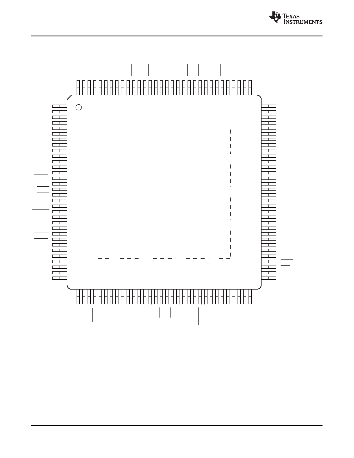
2.5 Terminal Assignments
The XIO2001 is available in either a 169-ball ZGU MicroStar BGA or a 144−ball ZAJ MicroStar BGA
package.
Figure 2-1 shows a terminal diagram of the ZGU package.
Figure 2-2 shows a terminal diagram of the ZAJ package.
Figure 2-3 shows a terminal diagram of the PNP package.
Copyright © 2009–2010, Texas Instruments Incorporated Overview 11
Submit Documentation Feedback
Product Folder Link(s): XIO2001

1 2 3 4 5 6 7 8 9 10 11 12 13
N N
M M
L L
K K
J J
H H
G G
F F
E
AD15 AD14 AD13 VDD_33 VSS VSS VSS VSS VSS VSSA VSSA RXN RXP
E
D D
C C
B B
A A
1 2 3 4 5 6 7 8 9 10 11 12 13
C
/BE[3] AD25 AD27 AD30 AD31 INTB PRST SERIRQ GPIO0// GPIO2 GPIO3//SDA JTAG_TDI GRST
N
AD20 AD22 AD24 AD26 AD28 I
NTA INTC LOCK GPIO1// GP IO4// JTAG_TDO JTAG_TCK WAKE
M
L
K
J
H
S
TOP PERR SERR# VDD_15 VSS VSS VSS VSS VSS VDD_15 VSSA TXN TXP
G
F
PAR C
/BE[1] CLK VSS VSS VSS VSS VSS VSS VDD_15 VSS VSS VDDA_15
F
E
AD12 AD11 AD8 VSS VDD_33 VSS VDD_15 VSS VDD_33 VSS C
LKREQ VREG_PD33 VDDA_33
D
_SEL
C
B
PCIR
AD4 AD1 R
EQ0 GNT0 REQ1 CLKOUT2 REQ2 CLKOUT4 CLKOUT5 GNT4 RE Q5 CLKRUN_EN
A
AD16 AD17
PCIR
VSS VSS VSS VDD_15 VSS VDD_33 VSSA VDD_33_ REF0_PCIE REF1_PCIE
I
RDY FRAME C/BE[2] VDD _33 VSS VSS VSS VSS VSS VSS VDD_33_ VDD_33 VDD_33_
T
RDY DEVSEL VDD_33 VSS VSS VSS VSS VSS VSS VDD_15 PERST VSSA VDDA_15
CLKRUN
AD10 AD9 AD7 AD5 AD0 GNT1 VDD_33 REQ3 REQ4 EXT_ARB_EN VSSA REFCLK– REFCLK+
C/BE[0] AD6 AD3 AD2 CLKOUT0 CLKOUT1 CLKOUT3 GNT2 GNT3 GNT5 CLKOUT6 PCLK66_SEL REFCLK125
AUX COMB
COMB_IO
AD18 AD19 AD21 AD23 AD29 M66EN INTD VDD_33 JTAG_ JTAG_TMS VSS PME VDD_15_
TRST# COMB
PWR_OVRD SCL
XIO2001
SCPS212D–MAY 2009–REVISED JANUARY 2010
www.ti.com
Figure 2-1. XIO2001 ZGU MicroStar BGA Package (Bottom View)
12 Overview Copyright © 2009–2010, Texas Instruments Incorporated
Submit Documentation Feedback
Product Folder Link(s): XIO2001

1 2 3 4 5 6 7 8 9 10 11 12 13
N N
M M
L L
K K
J J
H H
G G
F F
E
AD13 AD12 AD14 VDD_33 VSS VSS VSS VSS VREG_PD33 VDDA_15 RXP
E
D D
C C
B B
A A
1 2 3 4 5 6 7 8 9 10 11 12 13
AD21 AD24 AD27 AD28 AD31 I
NTA INTD LOCK GPIO0// GPIO2 JTAG_TDO JTAG_TCK VDD_15_
N
AD18 AD22 C
/BE[3] AD25 AD29 M66EN INTC SERIRQ GPIO1// GPIO4_ GRS T PME REF0_PCIE
M
L
K
J
H
PAR S
ERR PERR VSS VDD_33 VDD_33 VDD_15 VSSA VDD_15 VSSA TXN
G
F
CLK AD15 C/BE[1]
VSS VDD_33 VDD_33 VDD_33 VSS VDD_15 VSS VSSA
F
E
AD11 AD9
PCIR
CLKREQ
VSSA RXN
D
C
B
AD7 AD4 AD3 R
EQ0 GNT0 GNT1 CLKOUT3 CLKOUT4 REQ4 CLKOUT5 PCLK66_ EXT_ARB_ REFCLK125
A
C/BE[2]
AD19 AD17 VDD_33_ VDD_33_ VDD_15
FRAME
TRDY
PCIR
VSS VSS VDD_15 VDD_15 VSS VDD_33 VDD_33_ VSSA
S
TOP DEVSEL IRDY VSS VDD_33 VDD_33 VDD_15 VSS PERST VDDA_15 TXP
CLKRUN
AD10 C/BE[0] AD5 AD2 AD1 REQ1 REQ2 REQ3 REQ5 CLKOUT6 CLKRUN_EN VDDA_33 REFCLK+
AD8 AD6 AD0 CLKOUT0 CLKOUT1 CLKOUT2 GNT2 GNT3 GNT4 GNT5 VSSA REFCLK-
AD16 AD20 AD23 AD26 AD30 INTB PRST GPIO3//SDA JTAG_ JTAG_TDI JTAG_TMS WAKE REF1_PCIE
T
RST
PWR_OVRD SCL
COMB
SEL EN _SEL
AUX
COMB_IO COMB
XIO2001
www.ti.com
SCPS212D–MAY 2009–REVISED JANUARY 2010
Figure 2-2. XIO2001 ZAJ MicroStar BGA Package (Bottom View)
Copyright © 2009–2010, Texas Instruments Incorporated Overview 13
Submit Documentation Feedback
Product Folder Link(s): XIO2001
1
8
11
24
5
16
19
29
3
12
15
27
7
20
23
31
2
10
13
26
6
18
21
30
4
14
17
28
9
22
25
32
96
89
86
73
92
81
78
68
94
85
82
70
90
77
74
66
95
87
84
71
91
79
76
67
93
83
80
69
88
75
72
65
33
40
43
56
37
48
51
61
35
44
47
59
39
52
55
63
34
42
45
58
38
50
53
62
36
46
49
60
41
54
57
64
128
121
118
105
124
113
110
100
126
117
114
102
122
109
106
98
127
119
116
103
123
111
108
99
125
115
112
101
120
107
104
97
AD7
VCCP
C/BE[0]
AD8
AD9
AD10
VDD_33
AD11
AD12
AD13
AD14
AD15
CLK
C/BE[1]
SERR
PERR
STOP
DEVSEL
PAR
VDD_33
VDD_15
TRDY
IRDY
FRAME
C/BE[2]
AD16
VCCP
AD17
AD18
AD19
AD20
AD21
AD26
AD25
AD24
C/BE[3]
AD23
AD22
VDD_33
AD27
AD28
AD29
AD30
AD31
M66EN
VDD_33
INTA
INTB
INTC
INTD
PRST
SERIRQ
VDD_15
LOCK
GPIO0 // CLKRUN
GPIO1 // PWR_OVER
GPIO2
GPIO3 // SDA
GPIO4 // SCL
JTAG_TRST
JTAG_TDO
VDD_33
JTAG_TDI
JTAG_TMS
CLKRUN_EN
JTAG_TCK
GRST
REFCLK125_SEL
REFCLK–
REFCLK+
VDDA_33_REF_CLK
CLKREQ
VREG_PD33
VSSA_PCIE
RXN
RXP
VSSA_PCIE
VDDA_15_PCIE_RX
VDDPLL_15_PCIE
VDD_15_PCIE
VSSA_PCIE
TXN
TXP
VSSA_PCIE
VDDA_15_PCIE_TX
PERST
VDD_15_MAIN
VDD_33_COMB
VDD_33_MAIN
VDD_33_AUX
REF1_PCIE
REF0_PCIE
VDD_33_COM_IO
VDD_15_COMB
WAKE
PME
AD6
AD5
VDD_33
VDD_33
AD4
AD3
AD2
AD1
AD0
CLKOUT0
REQ0
CLKOUT1
GNT0
REQ1
GNT1
CLKOUT2
VDD_15
CLKOUT3
REQ2
GNT2
REQ3
CLKOUT4
GNT3
REQ4
CLKOUT5
GNT4
REQ5
GNT5
VDD_33
CLKOUT6
PCLK66_SEL
EXT_ARB_EN
XIO2001
SCPS212D–MAY 2009–REVISED JANUARY 2010
www.ti.com
Figure 2-3. XIO2001 PNP PowerPad™ HTQFP Package (Top View)
Submit Documentation Feedback
Product Folder Link(s): XIO2001
14 Overview Copyright © 2009–2010, Texas Instruments Incorporated

XIO2001
www.ti.com
SCPS212D–MAY 2009–REVISED JANUARY 2010
2.6 Terminal Descriptions
The following tables give a description of the terminals. These terminals are grouped in tables by
functionality. Each table includes the terminal name, terminal number, I/O type, and terminal description.
The following list describes the different input/output cell types that appear in the terminal description
tables:
• HS DIFF IN = High speed differential input
• HS DIFF OUT = High speed differential output
• PCI BUS = PCI bus 3-state bidirectional buffer with 3.3-V or 5.0-V clamp rail.
• LV CMOS = 3.3-V low voltage CMOS input or output with 3.3-V clamp rail
• BIAS = Input/output terminals that generate a bias voltage to determine a driver's operating current
• Feed through = these terminals connect directly to macros within the part and not through an input or
output cell.
• PWR = Power terminal
• GND = Ground terminal
Table 2-1. Power Supply Terminals
SIGNAL DESCRIPTION
PCIR A01, K03 D03, J03 I/O Resistor PCI Rail. 5.0-V or 3.3-V PCI bus clamp voltage to set
V
DD_15
V
DDA_15
V
DD_33
V
DD_33_AUX
V
DDA_33
ZGU ZAJ PNP I/O EXTERNAL
BALL # BALL # PIN # TYPE PARTS
maximum I/O voltage tolerance of the secondary PCI
bus signals. Connect this terminal to the secondary
PCI bus I/O clamp rail through a 1kΩ resistor.
G04, K07, J08, H08, 21, 53, 113 PWR Bypass 1.5-V digital core power terminals
D07, H10, J07, G08, capacitors
G10, F10 N13, K13,
G11, F11
F13, H13 E12, H12 PWR Pi filter 1.5-V analog power terminal
E04, H03, E05, G06, 7, 19, 33, 46, PWR Bypass 3.3-V digital I/O power terminal
J04, L08, H07, G07, 62, 100, 111, capacitors
K09, D09, H06, F08, 126
C07, D05, F07, F06,
J12 J11
J11 J12 73 PWR Bypass 3.3-V auxiliary power terminal Note: This terminal is
capacitors connected to VSSthrough a pulldown resistor if no
auxiliary supply is present.
D13 C12 PWR Pi filter 3.3-V analog power terminal
Copyright © 2009–2010, Texas Instruments Incorporated Overview 15
Submit Documentation Feedback
Product Folder Link(s): XIO2001

XIO2001
SCPS212D–MAY 2009–REVISED JANUARY 2010
Table 2-2. Ground Terminals
SIGNAL ZGU BALL # ZAJ BALL # I/O TYPE DESCRIPTION
V
SS
D04, F04, H04, E06, F05, G05, H05, GND Digital ground terminals
K04, K05, K06, J05, J06, J09, H09,
K08, L11, J10, E09, E08, E07, F12
D10, D08, D06, ,F09
F11, F12
V
SS
E05, E06, E07, GND Ground terminals for thermally-enhanced package
E08, E09, F05,
F06, F07, F08,
F09, G05, G06,
G07, G08, G09,
H05, H06, H07,
H08, H09, J05,
J06, J07, J08,
J09
V
SSA
K10, C11, H12, G09, B12, J13, G12, GND Analog ground terminal
G11, E11, E10 F13, D12
Table 2-3. Combined Power Output Terminals
SIGNAL DESCRIPTION
V
DD_15_COMB
V
DD_33_COMB
V
DD_33_COMBIO
ZGU ZAJ PNP I/O EXTERNAL
BALL # BALL # PIN # TYPE PARTS
L13 N13 69 Internally-combined 1.5-V main and V
Feed Bypass
through capacitors
output for external bypass capacitor filtering.
Supplies all internal 1.5-V circuitry powered by V
Caution: Do not use this terminal to supply external
power to other devices.
J13 K12 75 Internally-combined 3.3-V main and V
Feed Bypass
through capacitors
output for external bypass capacitor filtering.
Supplies all internal 3.3-V circuitry powered by V
Caution: Do not use this terminal to supply external
power to other devices.
K11 K11 70 Internally-combined 3.3-V main and V
output for external bypass capacitor filtering.
Feed Bypass
through capacitors
Supplies all internal 3.3-V input/output circuitry
powered by V
AUX
.
Caution: Do not use this terminal to supply external
power to other devices.
AUX
AUX
AUX
www.ti.com
power
AUX
power
AUX
power
.
.
Table 2-4. PCI Express Terminals
SIGNAL DESCRIPTION
CLKREQ D11 D11 91 0 LV V
PERST H11 H11 77 I LV V
REFCLK125_SEL B13 A13 95 I LV V
16 Overview Copyright © 2009–2010, Texas Instruments Incorporated
ZGU ZAJ PNP I/O CELL CLAMP EXTERNAL
BALL # BALL # PIN # TYPE TYPE RAIL PARTS
CMOS
CMOS
CMOS reference clock input.
DD_33_
COMBIO
DD_33_
COMBIO
DD_33
–
–
Pullup or
pulldown 0 = 100-MHz differential common reference clock
resistor used.
Submit Documentation Feedback
Product Folder Link(s): XIO2001
Clock request. When asserted low, requests
upstream device start clock in cases where clock
may be removed in L1.
Note: Since CLKREQ is an open-drain output
buffer, a system side pullup resistor is required.
PCI Express reset input. The PERST signal
identifies when the system power is stable and
generates an internal power on reset.
Note: The PERST input buffer has hysteresis.
Reference clock select. This terminal selects the
1 = 125-MHz single-ended, reference clock used.
XIO2001
www.ti.com
SCPS212D–MAY 2009–REVISED JANUARY 2010
Table 2-4. PCI Express Terminals (continued)
SIGNAL DESCRIPTION
REFCLK+ C13 C13 93 DI HS DIFF V
REFCLK– C12 B13 94 DI HS DIFF V
REF0_PCIE K12 M13 71 I/O BIAS – External reference resistor + and – terminals for
REF1_PCIE K13 L13 72 setting TX driver current. An external resistance
RXP E13 E13 87 DI HS DIFF V
RXN E12 D13 88 IN – the differential receive pair for the single PCI
TXP G13 H13 80 DO HS DIFF V
TXN G12 G13 81 OUT the differential transmit pair for the single PCI
WAKE M13 L12 68 O LV V
ZGU ZAJ PNP I/O CELL CLAMP EXTERNAL
BALL # BALL # PIN # TYPE TYPE RAIL PARTS
IN comprise the differential input pair for the
IN comprise the differential input pair for the
CMOS
DD_33
DD_33
SS
DD_15
DD_33_
COMBIO
– 100-MHz system reference clock. For a
Capacitor
for VSSfor
single-
ended node
External
resistor
Series
capacitor
–
Reference clock. REFCLK+ and REFCLK–
single-ended, 125-MHz system reference clock,
use the REFCLK+ input.
Reference clock. REFCLK+ and REFCLK–
100-MHz system reference clock. For a
single-ended, 125-MHz system reference clock,
attach a capacitor from REFCLK– to VSS.
of 14,532-Ω is connected between REF0_PCIE
and REF1_PCIE terminals. To eliminate the need
for a custom resistor, two series resistors are
recommended: a 14.3-kΩ, 1% resistor and a
232-Ω, 1% resistor.
High-speed receive pair. RXP and RXN comprise
Express lane supported.
High-speed transmit pair. TXP and TXN comprise
Express lane supported.
Wake is an active low signal that is driven low to
reactivate the PCI Express link hierarchy’s main
power rails and reference clocks.
Note: Since WAKE is an open-drain output
buffer, a system side pullup resistor is required.
Table 2-5. PCI System Terminals
SIGNAL DESCRIPTION
AD31 N05 N05 44 I/O PCI PCIR PCI address data lines
AD30 N04 L05 43 Bus
AD29 L05 M05 42
AD28 M05 N04 41
AD27 N03 N03 40
AD26 M04 L04 39
AD25 N02 M04 38
AD24 M03 N02 37
AD23 L04 L03 35
AD22 M02 M02 34
AD21 L03 N01 32
AD20 M01 L02 31
AD19 L02 K02 30
AD18 L01 M01 29
AD17 K02 K03 28
AD16 K01 L01 26
AD15 E01 F02 12
AD14 E02 E03 11
AD13 E03 E01 10
AD12 D01 E02 9
AD11 D02 D01 8
AD10 C01 C01 6
AD9 C02 D02 5
AD8 D03 B01 4
AD7 C03 A01 1
AD6 B02 B03 128
AD5 C04 C03 127
AD4 A02 A02 125
AD3 B03 A03 124
AD2 B04 C04 123
AD1 A03 C05 122
AD0 C05 B04 121
ZGU ZAJ PNP I/O CELL CLAMP EXTERNAL
BALL # BALL # PIN # TYPE TYPE RAIL PARTS
–
Copyright © 2009–2010, Texas Instruments Incorporated Overview 17
Submit Documentation Feedback
Product Folder Link(s): XIO2001
XIO2001
SCPS212D–MAY 2009–REVISED JANUARY 2010
www.ti.com
Table 2-5. PCI System Terminals (continued)
SIGNAL DESCRIPTION
C/BE[3] N01 M03 36 I/O PCI PCIR PCI command byte enables
C/BE[2] J03 K01 25 Bus
C/BE[1] F02 F03 14
C/BE[0] B01 C02 3
CLK F03 F01 13 I PCI PCIR PCI clock input. This is the clock input
CLKOUT0 B05 B05 120 O PCI PCIR PCI clock outputs. These clock outputs
CLKOUT1 B06 B06 117 Bus are used to clock the PCI bus. If the
CLKOUT2 A07 B07 114 bridge PCI bus clock outputs are used,
CLKOUT3 B07 A07 112 – then CLKOUT6 must be connected to
CLKOUT4 A09 A08 107 the CLK input.
CLKOUT5 A10 A10 104
CLKOUT6 B11 C10 99
DEVSEL H02 H02 20 I/O PCI PCIR Pullup PCI device select
FRAME J02 J01 24 I/O PCI PCIR Pullup PCI frame
GNT5 B10 B11 101 O PCI PCIR PCI grant outputs. These signals are
GNT4 A11 B10 103 Bus used for arbitration when the PCI bus
GNT3 B09 B09 106 is the secondary bus and an external
GNT2 B08 B08 109 arbiter is not used. GNT0 is used as
GNT1 C06 A06 115 the REQ for the bridge when an
GNT0 A05 A05 118 external arbiter is used.
INTA M06 N06 47 I PCI PCIR PCI interrupts A–D. These signals are
INTB N06 L06 48 Bus interrupt inputs to the bridge on the
INTC M07 M07 49 secondary PCI bus.
INTD L07 N07 50
IRDY J01 H03 23 I/O PCI PCIR Pullup PCI initiator ready
LOCK M08 N08 54 I/O PCI PCIR This terminal functions as PCI LOCK
M66EN L06 M06 45 I PCI PCIR 66-MHz mode enable
PAR F01 G01 15 I/O PCI PCIR PCI bus parity
PERR G02 G03 17 I/O PCI PCIR Pullup PCI parity error
PME L12 M12 67 I LV V
ZGU ZAJ PNP I/O CELL CLAMP EXTERNAL
BALL # BALL # PIN # TYPE TYPE RAIL PARTS
–
Bus to the PCI bus core.
Bus resistor per
Bus resistor per
Bus resistor per
Bus when bit 12 (LOCK_EN) is set in the
Bus
Bus
Bus resistor per
CMOS
DD_33_
COMBIO
–
PCI spec
PCI spec
–
Pullup
resistor per
PCI spec
PCI spec
Pullup
resistor per
PCI spec
Pullup PCLK66_SEL is low then the
resistor per frequency will be 25 MHz.
PCI spec
–
PCI spec
Pullup
resistor per
PCI spec
general control register (see
Section 4.65).
Note: In lock mode, an external pullup
resistor is required to prevent the
LOCK signal from floating.
0 = Secondary PCI bus and clock
outputs operate at 33 MHz. If
1 = Secondary PCI bus and clock
outputs operate at 66 MHz. If
PCLK66_SEL is low then the
frequency will be 50 MHz.
Pullup resistor per PCI spec PCI power
management event. This terminal may
be used to detect PME events from a
PCI device on the secondary bus.
Note: The PME input buffer has
hysteresis.
18 Overview Copyright © 2009–2010, Texas Instruments Incorporated
Submit Documentation Feedback
Product Folder Link(s): XIO2001

XIO2001
www.ti.com
SCPS212D–MAY 2009–REVISED JANUARY 2010
Table 2-5. PCI System Terminals (continued)
SIGNAL DESCRIPTION
REQ5 A12 C09 102 I PCI PCIR PCI request inputs. These signals are
REQ4 C09 A09 105 Bus If unused, a used for arbitration on the secondary
REQ3 C08 C08 108 weak pullup PCI bus when an external arbiter is not
REQ2 A08 C07 110 resistor per used. REQ0 is used as the GNT for
REQ1 A06 C06 116 PCI spec the bridge when an external arbiter is
REQ0 A04 A04 119 used.
PRST N07 L07 51 O PCI PCIR PCI reset. This terminal is an output to
SERR G03 G02 16 I/O PCI PCIR Pullup PCI system error
STOP G01 H01 18 I/O PCI PCIR Pullup PCI stop
TRDY H01 J02 22 I/O PCI PCIR Pullup PCI target ready
ZGU ZAJ PNP I/O CELL CLAMP EXTERNAL
BALL # BALL # PIN # TYPE TYPE RAIL PARTS
Bus the secondary PCI bus.
–
Bus resistor per
PCI spec
Bus resistor per
PCI spec
Bus resistor per
PCI spec
Table 2-6. JTAG Terminals
SIGNAL DESCRIPTION
JTAG_TCK M12 N12 65 I LV V
JTAG_TDI N12 L10 63 I LV V
JTAG_TDO M11 N11 61 O LV V
JTAG_TMS L10 L11 64 I LV V
ZGU ZAJ PNP I/O CELL CLAMP EXTERNAL
BALL # BALL # PIN # TYPE TYPE RAIL PARTS
CMOS provides the clock for the internal TAP
DD_33
Optional pullup
resistor
CMOS instructions and data are received on
DD_33
Optional pullup Note: This terminal has an internal
resistor active pullup resistor. The pullup is
CMOS serial output for test instructions and
DD_33
–
CMOS received at JTAG_TMS is decoded by
DD_33
Optional pullup
resistor
JTAG test clock input. This signal
controller.
Note: This terminal has an internal
active pullup resistor. The pullup is
active at all times.
Note: This terminal should be tied to
ground or pulled low if JTAG is not
required.
JTAG test data input. Serial test
this terminal.
active at all times.
Note: This terminal can be left
unconnected if JTAG is not required.
JTAG test data output. This terminal the
data.
Note: This terminal can be left
unconnected if JTAG is not required.
JTAG test mode select. The signal
the internal TAP controller to control test
operations.
Note: This terminal has an internal
active pullup resistor. The pullup is
active at all times.
Note: This terminal can be left
unconnected if JTAG is not required.
Copyright © 2009–2010, Texas Instruments Incorporated Overview 19
Submit Documentation Feedback
Product Folder Link(s): XIO2001

XIO2001
SCPS212D–MAY 2009–REVISED JANUARY 2010
Table 2-6. JTAG Terminals (continued)
SIGNAL DESCRIPTION
JTAG_TRST L09 L09 60 I LV V
ZGU ZAJ PNP I/O CELL CLAMP EXTERNAL
BALL # BALL # PIN # TYPE TYPE RAIL PARTS
CMOS Optional for asynchronous initialization
DD_33
Optional pullup
resistor
JTAG test reset. This terminal provides
of the TAP controller.
Note: This terminal has an internal
active pullup resistor. The pullup is
active at all times.
Note: This terminal should be tied to
ground or pulled low if JTAG is not
required.
Table 2-7. Miscellaneous Terminals
SIGNAL DESCRIPTION
CLKRUN_E A13 C11 96 I LV V
N CMOS
EXT_ARB_ C10 A12 97 I LV V
EN CMOS
GPIO0 // N09 N09 55 I/O LV V
CLKRUN CMOS
GPIO1 // M09 M09 56 I/O LV V
PWR_OVR CMOS
D
GPIO2 N10 N10 57 I/O LV V
ZGU ZAJ PNP I/O CELL CLAMP EXTERNAL
BALL # BALL # PIN # TYPE TYPE RAIL PARTS
DD_33
Optional
pullup
resistor
DD_33
Optional
pullup
resistor
DD_33
Optional
pullup
resistor
DD_33
–
CMOS
DD_33
–
Clock run enable
0 = Clock run support disabled
1 = Clock run support enabled
Note: The CLKRUN_EN input buffer has an
internal active pulldown. This pulldown is active
at all times.
External arbiter enable
0 = Internal arbiter enabled
1 = External arbiter enabled
Note: The EXT_ARB_EN input buffer has an
internal active pulldown. This pulldown is active
at all times.
General-purpose I/O 0/clock run. This terminal
functions as a GPIO controlled by bit 0
(GPIO0_DIR) in the GPIO control register (see
Section 4.59) or the clock run terminal. This
terminal is used as clock run input when the
bridge is placed in clock run mode.
Note: In clock run mode, an external pullup
resistor is required to prevent the CLKRUN
signal from floating.
Note: This terminal has an internal active pullup
resistor. The pullup is only active when reset is
asserted or when the GPIO is configured as an
input.
General-purpose I/O 1/power override. This
terminal functions as a GPIO controlled by bit 1
(GPIO1_DIR) in the GPIO control register (see
Section 4.59) or the power override output
terminal. GPIO1 becomes PWR_OVRD when
bits 22:20 (POWER_OVRD) in the general
control register are set to 001b or 011b (see
Section 4.65).
Note: This terminal has an internal active pullup
resistor. The pullup is only active when reset is
asserted or when the GPIO is configured as an
input.
General-purpose I/O 2. This terminal functions
as a GPIO controlled by bit 2 (GPIO2_DIR) in
the GPIO control register (see Section 4.59).
Note: This terminal has an internal active pullup
resistor. The pullup is only active when reset is
asserted or when the GPIO is configured as an
input.
www.ti.com
20 Overview Copyright © 2009–2010, Texas Instruments Incorporated
Submit Documentation Feedback
Product Folder Link(s): XIO2001

XIO2001
www.ti.com
SCPS212D–MAY 2009–REVISED JANUARY 2010
Table 2-7. Miscellaneous Terminals (continued)
SIGNAL DESCRIPTION
GPIO3 // N11 L08 58 I/O LV V
SDA CMOS
GPIO4 // M10 M10 59 I/O LV V
SCL CMOS
GRST N13 M11 66 I LV V
PCLK66_SE B12 A11 98 I LV V
L CMOS
SERIRQ N08 M08 52 I/O PCI Bus PCIR
VREG_PD3 D12 E11 90 I LV V
3 CMOS
ZGU ZAJ PNP I/O CELL CLAMP EXTERNAL
BALL # BALL # PIN # TYPE TYPE RAIL PARTS
DD_33
Optional set in the Serial Bus Control and Status
pullup Register (see Section 4.58). If no pullup is
resistor detected then this terminal functions as GPIO3.
DD_33
Optional
pullup
resistor
CMOS
DD_33
_COMBIO
–
DD_33
Optional
pulldown
resistor
Pullup or
pulldown
resistor
DD_33
_COMBIO
Pulldown terminal should always be tied directly to
resistor ground or an optional pulldown resistor can be
GPIO3 or serial-bus data. This terminal
functions as serial-bus data if a pullup resistor is
detected on SCL or when the SBDETECT bit is
Note: In serial-bus mode, an external pullup
resistor is required to prevent the SDA signal
from floating.
GPIO4 or serial-bus clock. This terminal
functions as serial-bus clock if a pullup resistor
is detected on SCL or when the SBDETECT bit
is set in the Serial Bus Control and Status
Register (see Section 4.58). If no pullup is
detected then this terminal functions as GPIO4.
Note: In serial-bus mode, an external pullup
resistor is required to prevent the SCL signal
from floating.
Note: This terminal has an internal active pullup
resistor. The pullup is only active when reset is
asserted or when the GPIO is configured as an
input.
Global reset input. Asynchronously resets all
logic in device, including sticky bits and power
management state machines.
Note: The GRST input buffer has both
hysteresis and an internal active pullup. The
pullup is active at all times.
PCI clock select. This terminal determines the
default PCI clock frequency driven out the
CLKOUTx terminals.
0 = 50 MHz PCI Clock
1 = 66 MHz PCI Clock
Note: This terminal has an internal active pullup
resistor. This pullup is active at all times.
Note: M66EN terminal also has an affect of PCI
clock frequency.
Serial IRQ interface. This terminal functions as
a serial IRQ interface if a pullup is detected
when PERST is deasserted. If a pulldown is
detected, then the serial IRQ interface is
disabled.
3.3-V voltage regulator powerdown. This
used.
Copyright © 2009–2010, Texas Instruments Incorporated Overview 21
Submit Documentation Feedback
Product Folder Link(s): XIO2001
PCI Express
Transmitter
PCI Express
Receiver
PCI Bus Interface
Configuration and
Memory Register
GPIO
Serial
EEPROM
Serial
IRQ
Reset
Controller
Clock
Generator
Power
Mgmt
XIO2001
SCPS212D–MAY 2009–REVISED JANUARY 2010
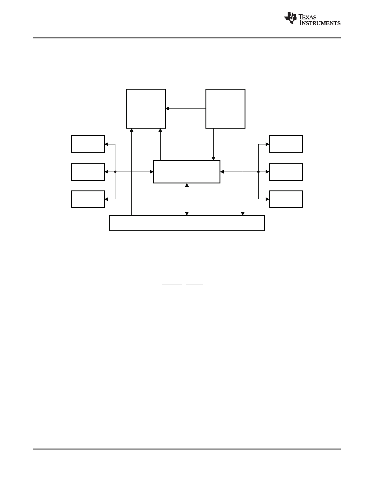
3 Feature/Protocol Descriptions
This chapter provides a high-level overview of all significant device features. Figure 3-1 shows a simplified
block diagram of the basic architecture of the PCI-Express to PCI Bridge. The top of the diagram is the
PCI Express interface and the PCI bus interface is located at the bottom of the diagram.
www.ti.com
Figure 3-1. XIO2001 Block Diagram
3.1 Power-Up/-Down Sequencing
The bridge contains both 1.5-V and 3.3-V power terminals. The following power-up and power-down
sequences describe how power is applied to these terminals.
In addition, the bridge has three resets: PERST, GRST and an internal power-on reset. These resets are
fully described in Section 3.2. The following power-up and power-down sequences describe how PERST
is applied to the bridge.
The application of the PCI Express reference clock (REFCLK) is important to the power-up/-down
sequence and is included in the following power-up and power-down descriptions.
22 Feature/Protocol Descriptions Copyright © 2009–2010, Texas Instruments Incorporated
Submit Documentation Feedback
Product Folder Link(s): XIO2001
V and
DD_15
V
DDA_15
REFCLK
PERST
100 ms
100 ms
V and
DD_33
V
DDA_33
PCIR
XIO2001
www.ti.com
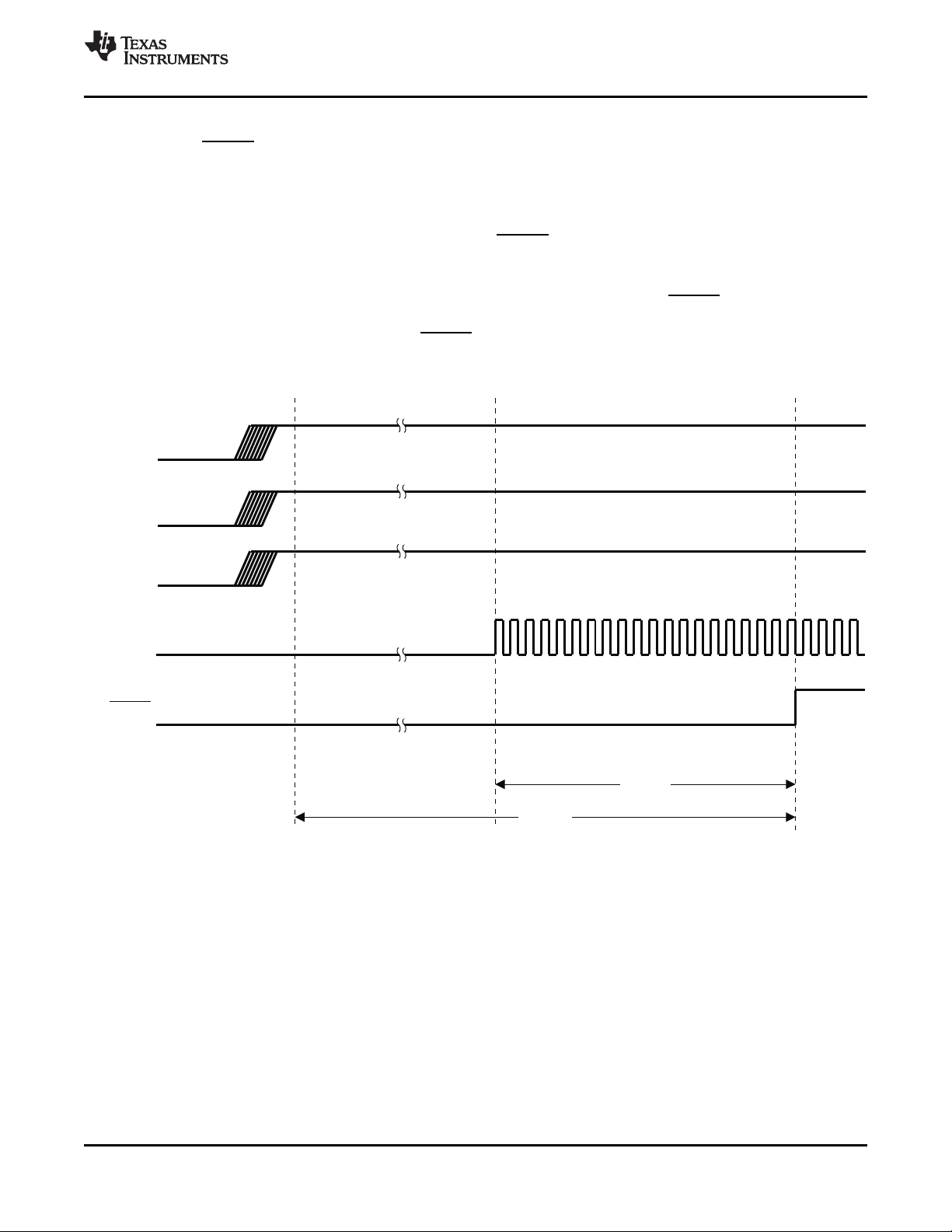
3.1.1 Power-Up Sequence
1. Assert PERST to the device.
2. Apply 1.5-V and 3.3-V voltages.
3. Apply PCIR clamp voltage.
4. Apply a stable PCI Express reference clock.
5. To meet PCI Express specification requirements, PERST cannot be deasserted until the following two
delay requirements are satisfied:
– Wait a minimum of 100 ms after applying a stable PCI Express reference clock. The 100-ms limit
satisfies the requirement for stable device clocks by the deassertion of PERST.
– Wait a minimum of 100 ms after applying power. The 100-ms limit satisfies the requirement for
stable power by the deassertion of PERST.
See the power-up sequencing diagram in Figure 3-2.
SCPS212D–MAY 2009–REVISED JANUARY 2010
Figure 3-2. Power-Up Sequence
Copyright © 2009–2010, Texas Instruments Incorporated Feature/Protocol Descriptions 23
Submit Documentation Feedback
Product Folder Link(s): XIO2001
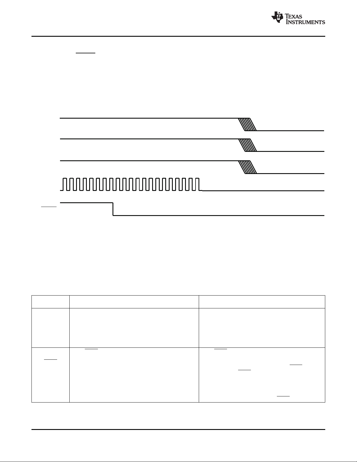
V and
DD_15
V
DDA_15
V and
DD_33
V
DDA_33
PCIR
REFCLK
PERST
XIO2001
SCPS212D–MAY 2009–REVISED JANUARY 2010
3.1.2 Power-Down Sequence
1. Assert PERST to the device.
2. Remove the reference clock.
3. Remove PCIR clamp voltage.
4. Remove 3.3-V and 1.5-V voltages.
See the power-down sequencing diagram in Figure 3-3. If the V
after a system shutdown, then the bridge power-down sequence is exactly the same as shown in
Figure 3-3.
DD_33_AUX
www.ti.com
terminal is to remain powered
Figure 3-3. Power-Down Sequence
3.2 Bridge Reset Features
There are five bridge reset options that include internally-generated power-on reset, resets generated by
asserting input terminals, and software-initiated resets that are controlled by sending a PCI Express hot
reset or setting a configuration register bit. Table 3-1 identifies these reset sources and describes how the
bridge responds to each reset.
Table 3-1. XIO2001 Reset Options
RESET XIO2001 FEATURE RESET RESPONSE
OPTION
Bridge During a power-on cycle, the bridge asserts an internal reset When the internal power-on reset is asserted, all control
internally- and monitors the V
generated reaches 90% of the nominal input voltage specification, management state machines are initialized to their default
power-on reset power is considered stable. After stable power, the bridge state.
monitors the PCI Express reference clock (REFCLK) and In addition, the XIO2001 asserts the internal PCI bus reset.
waits 10 ms after active clocks are detected. Then, internal
power-on reset is deasserted.
Global reset When GRST is asserted low, an internal power-on reset When GRST is asserted low, all control registers, state
input occurs. This reset is asynchronous and functions during machines, sticky register bits, and power management
GRST both normal power states and V
DD_15_COMB
terminal. When this terminal registers, state machines, sticky register bits, and power
power states. state machines are initialized to their default state. In
AUX
addition, the bridge asserts PCI bus reset (PRST). When
the rising edge of GRST occurs, the bridge samples the
state of all static control inputs and latches the information
internally. If an external serial EEPROM is detected, then a
download cycle is initiated. Also, the process to configure
and initialize the PCI Express link is started. The bridge
starts link training within 80 ms after GRST is deasserted.
24 Feature/Protocol Descriptions Copyright © 2009–2010, Texas Instruments Incorporated
Submit Documentation Feedback
Product Folder Link(s): XIO2001

XIO2001
www.ti.com
SCPS212D–MAY 2009–REVISED JANUARY 2010
Table 3-1. XIO2001 Reset Options (continued)
RESET XIO2001 FEATURE RESET RESPONSE
OPTION
PCI Express This XIO2001 input terminal is used by an upstream PCI When PERST is asserted low, all control register bits that
reset input Express device to generate a PCI Express reset and to are not sticky are reset. Within the configuration register
PERST signal a system power good condition. maps, the sticky bits are indicated by the ┦ symbol. Also,
When PERST is asserted low, the XIO2001 generates an
internal PCI Express reset as defined in the PCI Express
specification.
When PERST transitions from low to high, a system power In addition, the XIO2001 asserts the internal PCI bus reset.
good condition is assumed by the XIO2001.
Note: The system must assert PERST before power is When the rising edge of PERST occurs, the XIO2001
removed, before REFCLK is removed or before REFCLK samples the state of all static control inputs and latches
becomes unstable. the information internally. If an external serial EEPROM is
PCI Express The XIO2001 responds to a training control hot reset In the DL_DOWN state, all remaining configuration register
training control received on the PCI Express interface. After a training bits and state machines are reset. All remaining bits
hot reset control hot reset, the PCI Express interface enters the exclude sticky bits and EEPROM loadable bits. All
DL_DOWN state. remaining state machines exclude sticky functionality and
PCI bus reset System software has the ability to assert and deassert the When bit 6 (SRST) in the bridge control register at offset
PRST PRST terminal on the secondary PCI bus interface. This 3Eh (see Section 4.29) is asserted, the bridge asserts the
terminal is the PCI bus reset. PRST terminal. A 0 in the SRST bit deasserts the PRST
all state machines that are not associated with sticky
functionality are reset.
detected, then a download cycle is initiated. Also, the
process to configure and initialize the PCI Express link is
started. The XIO2001 starts link training within 80 ms after
PERST is deasserted.
EEPROM functionality.
Within the configuration register maps, the sticky bits are
indicated by the ┦ symbol and the EEPROM loadable bits
are indicated by the † symbol.
In addition, the XIO2001 asserts the internal PCI bus reset.
terminal.
3.3 PCI Express Interface
3.3.1 External Reference Clock
The bridge requires either a differential, 100-MHz common clock reference or a single-ended, 125-MHz
clock reference. The selected clock reference must meet all PCI Express Electrical Specification
requirements for frequency tolerance, spread spectrum clocking, and signal electrical characteristics.
Spread Spectrum is an optional feature of the PCI Express Electrical Specification that is supported by
this bridge.
If the REFCLK125_SEL input is connected to VSS, then a differential, 100-MHz common clock reference is
expected by the XIO2001. If the REFCLK125_SEL terminal is connected to V
125-MHz clock reference is expected by the bridge
When the single-ended, 125-MHz clock reference option is enabled, the single-ended clock signal is
connected to the REFCLK+ terminal. The REFCLK– terminal is connected to one side of an external
capacitor with the other side of the capacitor connected to VSS.
When using a single-ended reference clock, care must be taken to ensure interoperability from a system
jitter standpoint. The PCI Express Base Specification does not ensure interoperability when using a
differential reference clock commonly used in PC applications along with a single-ended clock in a
non-common clock architecture. System jitter budgets will have to be verified to ensure interoperability.
See the PCI Express Jitter and BER White Paper from the PCI-SIG.
, then a single-ended,
DD_33
Copyright © 2009–2010, Texas Instruments Incorporated Feature/Protocol Descriptions 25
Submit Documentation Feedback
Product Folder Link(s): XIO2001

XIO2001
SCPS212D–MAY 2009–REVISED JANUARY 2010
3.3.2 Beacon
The bridge supports the PCI Express in-band beacon feature. Beacon is driven on the upstream PCI
Express link by the bridge to request the reapplication of main power when in the L2 link state. To enable
the beacon feature, bit 10 (BEACON_ENABLE) in the general control register at offset D4h is asserted.
See Section 4.65, General Control Register, for details.
If the bridge is in the L2 link state and beacon is enabled, when a secondary PCI bus device asserts PME,
then the bridge outputs the beacon signal on the upstream PCI Express link. The beacon signal frequency
is approximately 500 kHz ± 50% with a differential peak-to-peak amplitude of 500 mV and no
de-emphasis. Once the beacon is activated, the bridge continues to send the beacon signal until main
power is restored as indicated by PERST going inactive. At this time, the beacon signal is deactivated.
3.3.3 Wake
The bridge supports the PCI Express sideband WAKE feature. WAKE is an active low signal driven by the
bridge to request the reapplication of main power when in the L2 link state. Since WAKE is an
open-collector output, a system-side pullup resistor is required to prevent the signal from floating.
When the bridge is in the L2 link state and PME is received from a device on the secondary PCI bus, the
WAKE signal is asserted low as a wakeup mechanism. Once WAKE is asserted, the bridge drives the
signal low until main power is restored as indicated by PERST going inactive. At this time, WAKE is
deasserted.
3.3.4 Initial Flow Control Credits
www.ti.com
The bridge flow control credits are initialized using the rules defined in the PCI Express Base
Specification. Table 3-2 identifies the initial flow control credit advertisement for the bridge.
Table 3-2. Initial Flow Control Credit Advertisements
CREDIT TYPE INITIAL ADVERTISEMENT
Posted request headers (PH) 8
Posted request data (PD) 128
Non-posted header (NPH) 4
Non-posted data (NPD) 4
Completion header (CPLH) 0 (infinite)
Completion data (CPLD) 0 (infinite)
3.3.5 PCI Express Message Transactions
PCI Express messages are both initiated and received by the bridge. Table 3-3 outlines message support
within the bridge.
Table 3-3. Messages Supported by the Bridge
MESSAGE SUPPORTED BRIDGE ACTION
Assert_INTx Yes Transmitted upstream
Deassert_INTx Yes Transmitted upstream
PM_Active_State_Nak Yes Received and processed
PM_PME Yes Transmitted upstream
PME_Turn_Off Yes Received and processed
PME_TO_Ack Yes Transmitted upstream
ERR_COR Yes Transmitted upstream
ERR_NONFATAL Yes Transmitted upstream
26 Feature/Protocol Descriptions Copyright © 2009–2010, Texas Instruments Incorporated
Submit Documentation Feedback
Product Folder Link(s): XIO2001
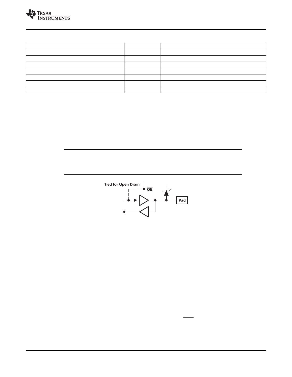
PCIR
XIO2001
www.ti.com
SCPS212D–MAY 2009–REVISED JANUARY 2010
Table 3-3. Messages Supported by the Bridge (continued)
MESSAGE SUPPORTED BRIDGE ACTION
ERR_FATAL Yes Transmitted upstream
Set_Slot_Power_Limit Yes Received and processed
Unlock No Discarded
Hot plug messages No Discarded
Advanced switching messages No Discarded
Vendor defined type 0 No Unsupported request
Vendor defined type 1 No Discarded
All supported message transactions are processed per the PCI Express Base Specification.
3.4 PCI Bus Interface
3.4.1 I/O Characteristics
Figure 3-4 shows a 3-state bi-directional buffer that represents the I/O cell design for the PCI bus.
Section 7.7, Electrical Characteristics over Recommended Operating Conditions, provides the electrical
characteristics of the PCI bus I/O cell.
NOTE
The PCI bus interface on the bridge meets the ac specifications of the PCI Local Bus
Specification. Additionally, PCI bus terminals (input or I/O) must be held high or low to
prevent them from floating.
Figure 3-4. 3-State Bidirectional Buffer
3.4.2 Clamping Voltage
In the bridge, the PCI bus I/O drivers are powered from the V
tolerant to input signals with 5-V peak-to-peak amplitudes.
For PCI bus interfaces operating at 50MHz or 66 MHz, all devices are required to output only 3.3-V
peak-to-peak signal amplitudes. For PCI bus interfaces operating at 25-MHz or 33-MHz, devices may
output either 3.3-V or 5-V peak-to-peak signal amplitudes. The bridge accommodates both signal
amplitudes.
Each PCI bus I/O driver cell has a clamping diode connected to the internal V
the cell from excessive input voltage. The internal V
rail is connected to two PCIR terminals. If the PCI
CCP
signaling is 3.3-V, then PCIR terminals are connected to a 3.3-V power supply via a 1kΩ resistor. If the
PCI signaling is 5-V, then the PCIR terminals are connected to a 5-V power supply via a 1kΩ resistor.
The PCI bus signals attached to the V
clamping voltage are identified as follows
CCP
• Table 2-5, PCI System Terminals, all terminal names except for PME
• Table 2-7, Miscellaneous Terminals, the terminal name SERIRQ.
Copyright © 2009–2010, Texas Instruments Incorporated Feature/Protocol Descriptions 27
Submit Documentation Feedback
Product Folder Link(s): XIO2001
power rail. Plus, the I/O driver cell is
DD_33
voltage rail that protects
CCP

XIO2001
SCPS212D–MAY 2009–REVISED JANUARY 2010
3.4.3 PCI Bus Clock Run
The bridge supports the clock run protocol as specified in the PCI Mobile Design Guide. When the clock
run protocol is enabled, the bridge assumes the role of the central resource master.
To enable the clock run function, terminal CLKRUN_EN is asserted high. Then, terminal GPIO0 is enabled
as the CLKRUN signal. An external pullup resistor must be provided to prevent the CLKRUN signal from
floating To verify the operational status of the PCI bus clocks, bit 0 (SEC_CLK_STATUS) in the clock run
status register at offset DAh (see Section 4.68) is read.
Since the bridge has several unique features associated with the PCI bus interface, the system designer
must consider the following interdependencies between these features and the CLKRUN feature:
1. If the system designer chooses to generate the PCI bus clock externally, then the CLKRUN mode of
the bridge must be disabled. The central resource function within the bridge only operates as a
CLKRUN master and does not support the CLKRUN slave mode.
2. If the central resource function has stopped the PCI bus clocks, then the bridge still detects INTx state
changes and will generate and send PCI Express messages upstream.
3. If the serial IRQ interface is enabled and the central resource function has stopped the PCI bus clocks,
then any PCI bus device that needs to report an IRQ interrupt asserts CLKRUN to start the bus clocks.
4. When a PCI bus device asserts CLKRUN, the central resource function turns on PCI bus clocks for a
minimum of 512 cycles.
5. If the serial IRQ function detects an IRQ interrupt, then the central resource function keeps the PCI bus
clocks running until the IRQ interrupt is cleared by software.
6. If the central resource function has stopped the PCI bus clocks and the bridge receives a downstream
transaction that is forwarded to the PCI bus interface, then the bridge asserts CLKRUN to start the bus
clocks.
7. The central resource function is reset by PCI bus reset (PRST) assuring that clocks are present during
PCI bus resets.
www.ti.com
3.4.4 PCI Bus External Arbiter
The bridge supports an external arbiter for the PCI bus. Terminal (EXT_ARB_EN), when asserted high,
enables the use of an external arbiter.
When an external arbiter is enabled, GNT0 is connected to the external arbiter as the REQ for the bridge.
Likewise, REQ0 is connected to the external arbiter as the GNT for the bridge.
3.4.5 MSI Messages Generated from the Serial IRQ Interface
When properly configured, the bridge converts PCI bus serial IRQ interrupts into PCI Express message
signaled interrupts (MSI). classic PCI configuration register space is provided to enable this feature. The
following list identifies the involved configuration registers:
1. Command register at offset 04h, bit 2 (MASTER_ENB) is asserted (see Table 4-2).
2. MSI message control register at offset 52h, bits 0 (MSI_EN) and 6:4 (MM_EN) enable single and
multiple MSI messages, respectively (see Section 4.42).
3. MSI message address register at offsets 54h and 58h specifies the message memory address. A
nonzero address value in offset 58h initiates 64-bit addressing (see Section 4.37 and Section 4.44).
4. MSI message data register at offset 5Ch specifies the system interrupt message (see Section 4.45).
5. Serial IRQ mode control register at offset E0h specifies the serial IRQ bus format (see Section 4.72).
6. Serial IRQ edge control register at offset E2h selects either level or edge mode interrupts (see
Section 4.73).
7. Serial IRQ status register at offset E4h reports level mode interrupt status (see Section 4.74).
28 Feature/Protocol Descriptions Copyright © 2009–2010, Texas Instruments Incorporated
Submit Documentation Feedback
Product Folder Link(s): XIO2001

XIO2001
www.ti.com
SCPS212D–MAY 2009–REVISED JANUARY 2010
A PCI Express MSI is generated based on the settings in the serial IRQ edge control register. If the
system is configured for edge mode, then an MSI message is sent when the corresponding serial IRQ
interface sample phase transitions from low to high. If the system is configured for level mode, then an
MSI message is sent when the corresponding IRQ status bit in the serial IRQ status register changes from
low to high.
The bridge has a dedicated SERIRQ terminal for all PCI bus devices that support serialized interrupts.
This SERIRQ interface is synchronous to the PCI bus clock input (CLK) frequency. The bridge always
generates a 17-phase serial IRQ stream. Internally, the bridge detects only 16 IRQ interrupts, IRQ0 frame
through IRQ15 frame. The IOCHCK frame is not monitored by the serial IRQ state machine and never
generates an IRQ interrupt or MSI message.
The multiple message enable (MM_EN) field determines the number of unique MSI messages that are
sent upstream on the PCI Express link. From 1 message to 16 messages, in powers of 2, are selectable.
If fewer than 16 messages are selected, then the mapping from IRQ interrupts to MSI messages is
aliased. Table 3-4 illustrates the IRQ interrupt to MSI message mapping based on the number of enabling
messages.
Table 3-4. IRQ Interrupt to MSI Message Mapping
IRQ 1 MESSAGE 2 MESSAGES 4 MESSAGES 16 MESSAGES
INTERRUPT ENABLED ENABLED ENABLED ENABLED
IRQ0 MSI MSG #0 MSI MSG #0 MSI MSG #0 MSI MSG #0 MSI MSG #0
IRQ1 MSI MSG #0 MSI MSG #1 MSI MSG #1 MSI MSG #1 MSI MSG #1
IRQ2 MSI MSG #0 MSI MSG #0 MSI MSG #2 MSI MSG #2 MSI MSG #2
IRQ3 MSI MSG #0 MSI MSG #1 MSI MSG #3 MSI MSG #3 MSI MSG #3
IRQ4 MSI MSG #0 MSI MSG #0 MSI MSG #0 MSI MSG #4 MSI MSG #4
IRQ5 MSI MSG #0 MSI MSG #1 MSI MSG #1 MSI MSG #5 MSI MSG #5
IRQ6 MSI MSG #0 MSI MSG #0 MSI MSG #2 MSI MSG #6 MSI MSG #6
IRQ7 MSI MSG #0 MSI MSG #1 MSI MSG #3 MSI MSG #7 MSI MSG #7
IRQ8 MSI MSG #0 MSI MSG #0 MSI MSG #0 MSI MSG #0 MSI MSG #8
IRQ9 MSI MSG #0 MSI MSG #1 MSI MSG #1 MSI MSG #1 MSI MSG #9
IRQ10 MSI MSG #0 MSI MSG #0 MSI MSG #2 MSI MSG #2 MSI MSG #10
IRQ11 MSI MSG #0 MSI MSG #1 MSI MSG #3 MSI MSG #3 MSI MSG #11
IRQ12 MSI MSG #0 MSI MSG #0 MSI MSG #0 MSI MSG #4 MSI MSG #12
IRQ13 MSI MSG #0 MSI MSG #1 MSI MSG #1 MSI MSG #5 MSI MSG #13
IRQ14 MSI MSG #0 MSI MSG #0 MSI MSG #2 MSI MSG #6 MSI MSG #14
IRQ15 MSI MSG #0 MSI MSG #1 MSI MSG #3 MSI MSG #7 MSI MSG #15
8 MESSAGES ENABLED
The MSI message format is compatible with the PCI Express request header format for 32-bit and 64-bit
memory write transactions. The system message and message number fields are included in bytes 0 and
1 of the data payload.
3.4.6 PCI Bus Clocks
The bridge has seven PCI bus clock outputs and one PCI bus clock input. Up to six PCI bus devices are
supported by the bridge.
Terminal PCLK66_SEL selects the default operating frequency. This signal works in conjunction with
terminal M66EN to determine the final output frequency. When PCLK66_SEL is asserted high then the
clock frequency will be either 66-MHz or 33-MHz depending on the state of M66EN. When M66EN is
asserted high then the clock frequency will be 66-MHz, when M66EN is de-asserted the clock frequency
Copyright © 2009–2010, Texas Instruments Incorporated Feature/Protocol Descriptions 29
Submit Documentation Feedback
Product Folder Link(s): XIO2001
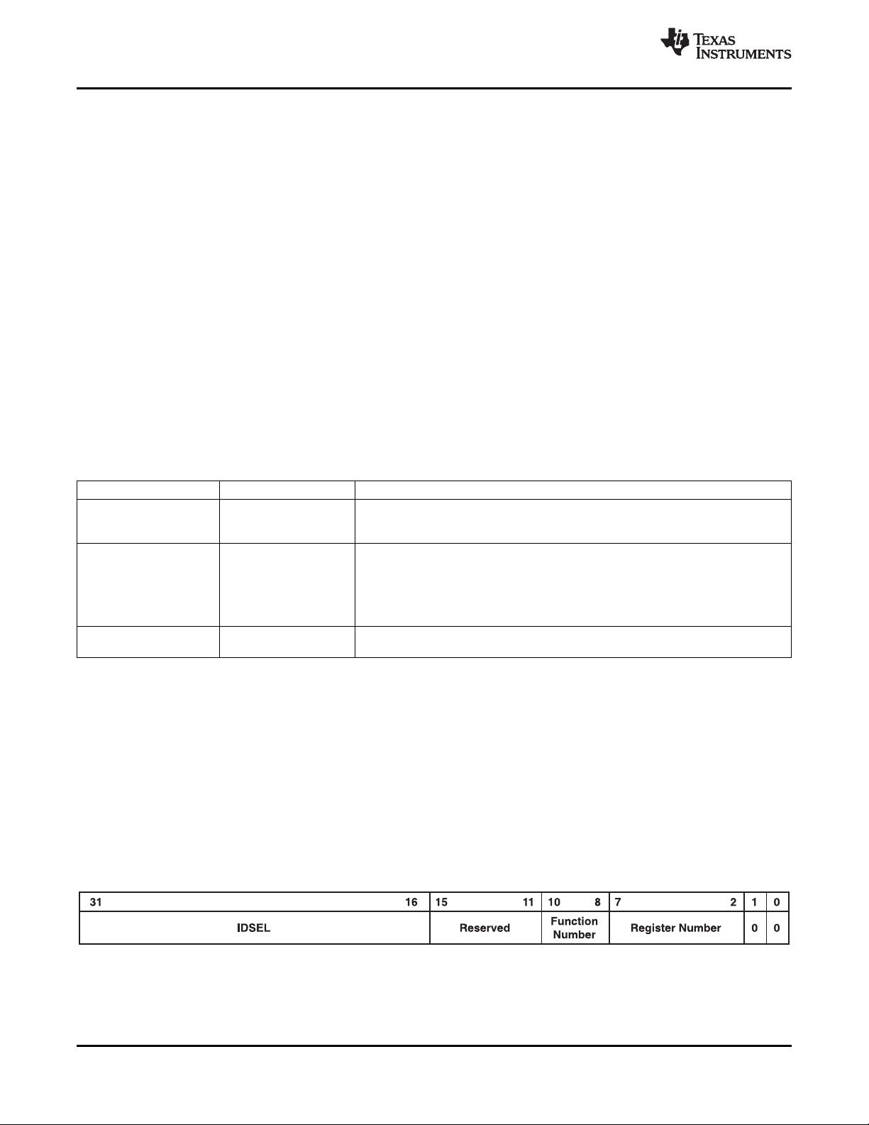
XIO2001
SCPS212D–MAY 2009–REVISED JANUARY 2010
will be 33-MHz. When PCLK66_SEL is de-asserted then the clock frequency will be either 50-MHz or
25-MHz. When M66EN is asserted high then the clock frequency will be 50-MHz, when M66EN is
de-asserted the clock frequency will be 25-MHz. The clock control register at offset D8h provides 7 control
bits to individually enable or disable each PCI bus clock output (see Section 4.66). The register default is
enabled for all 7 outputs.
The PCI bus clock (CLK) input provides the clock to the internal PCI bus core and serial IRQ core. When
the internal PCI bus clock source is selected, PCI bus clock output 6 (CLKOUT6) is connected to the PCI
bus clock input (CLK). When an external PCI bus clock source is selected, the external clock source is
connected to the PCI bus clock input (CLK). For external clock mode, all seven CLKOUT6:0 terminals
must be disabled using the clock control register at offset D8h (see Section 4.66).
3.5 PCI Port Arbitration
The internal PCI port arbitration logic supports up to six external PCI bus devices plus the bridge. This
bridge supports a classic PCI arbiter.
3.5.1 Classic PCI Arbiter
The classic PCI arbiter is configured through the classic PCI configuration space at offset DCh. Table 3-5
identifies and describes the registers associated with classic PCI arbitration mode.
Table 3-5. Classic PCI Arbiter Registers
PCI OFFSET REGISTER NAME DESCRIPTION
Classic PCI configuration Arbiter control
register DCh (see Section 4.69)
Classic PCI configuration Arbiter request mask status if a PCI device does not respond within 16 PCI bus clocks. Bit 6
register DDh (see Section 4.70) (AUTO_MASK) in the arbiter request mask register automatically masks a PCI bus
Classic PCI configuration Arbiter time-out status When bit 7 (ARB_TIMEOUT) in the arbiter request mask register is asserted,
register DEh (see Section 4.71) timeout status for each PCI bus device is reported in this register.
Contains a two-tier priority scheme for the bridge and six PCI bus devices. The
bridge defaults to the high priority tier. The six PCI bus devices default to the low
priority tier. A bus parking control bit (bit 7, PARK) is provided.
Six mask bits provide individual control to block each PCI Bus REQ input. Bit 7
(ARB_TIMEOUT) in the arbiter request mask register enables generating timeout
REQ if the device does not respond after GNT is issued. The AUTO_MASK bit is
cleared to disable any automatically generated mask.
www.ti.com
3.6 Configuration Register Translation
PCI Express configuration register transactions received by the bridge are decoded based on the
transaction’s destination ID. These configuration transactions can be broken into three subcategories: type
0 transactions, type 1 transactions that target the secondary bus, and type 1 transactions that target a
downstream bus other than the secondary bus.
PCI Express type 0 configuration register transactions always target the configuration space and are never
passed on to the secondary interface.
Type 1 configuration register transactions that target a device on the secondary bus are converted to type
0 configuration register transactions on the PCI bus. Figure 3-5 shows the address phase of a type 0
configuration transaction on the PCI bus as defined by the PCI specification.
Figure 3-5. Type 0 Configuration Transaction Address Phase Encoding
In addition, the bridge converts the destination ID device number to one of the AD[31:16] lines as the
IDSEL signal. The implemented IDSEL signal mapping is shown in Table 3-6.
30 Feature/Protocol Descriptions Copyright © 2009–2010, Texas Instruments Incorporated
Submit Documentation Feedback
Product Folder Link(s): XIO2001

XIO2001
www.ti.com
SCPS212D–MAY 2009–REVISED JANUARY 2010
Table 3-6. Type 0 Configuration Transaction
IDSEL Mapping
DEVICE
NUMBER
00000 0000 0000 0000 0001
00001 0000 0000 0000 0010
00010 0000 0000 0000 0100
00011 0000 0000 0000 1000
00100 0000 0000 0001 0000
00101 0000 0000 0010 0000
00110 0000 0000 0100 0000
00111 0000 0000 1000 0000
01000 0000 0001 0000 0000
01001 0000 0010 0000 0000
01010 0000 0100 0000 0000
01011 0000 1000 0000 0000
01100 0001 0000 0000 0000
01101 0010 0000 0000 0000
01110 0100 0000 0000 0000
01111 1000 0000 0000 0000
1xxxx 0000 0000 0000 0000
AD[31:16]
Type 1 configuration registers transactions that target a downstream bus other then the secondary bus are
output on the PCI bus as type 1 PCI configuration transactions. Figure 3-6 shows the address phase of a
type 1 configuration transaction on the PCI bus as defined by the PCI specification.
Figure 3-6. Type 1 Configuration Transaction Address Phase Encoding
Copyright © 2009–2010, Texas Instruments Incorporated Feature/Protocol Descriptions 31
Submit Documentation Feedback
Product Folder Link(s): XIO2001

XIO2001
SCPS212D–MAY 2009–REVISED JANUARY 2010
3.7 PCI Interrupt Conversion to PCI Express Messages
The bridge converts interrupts from the PCI bus sideband interrupt signals to PCI Express interrupt
messages.
Table 3-7, Figure 3-7, and Figure 3-8 illustrate the format for both the assert and deassert INTx
messages.
Table 3-7. Interrupt Mapping
In The Code Field
INTERRUPT CODE FIELD
INTA 00
INTB 01
INTC 10
INTD 11
www.ti.com
Figure 3-7. PCI Express ASSERT_INTX Message
Figure 3-8. PCI Express DEASSERT_INTX Message
3.8 PME Conversion to PCI Express Messages
When the PCI bus PME input transitions low, the bridge generates and sends a PCI Express PME
message upstream. The requester ID portion of the PME message uses the stored value in the secondary
bus number register as the bus number, 0 as the device number, and 0 as the function number. The Tag
field for each PME message is 00h. A PME message is sent periodically until the PME signal transitions
high.
Figure 3-9 illustrates the format for a PCI Express PME message.
32 Feature/Protocol Descriptions Copyright © 2009–2010, Texas Instruments Incorporated
Submit Documentation Feedback
Product Folder Link(s): XIO2001

DataAddress
CLK
FRAME
LOCK
AD
IRDY
TRDY
DEVSEL
XIO2001
www.ti.com
Figure 3-9. PCI Express PME Message
3.9 PCI Express to PCI Bus Lock Conversion
The bus-locking protocol defined in the PCI Express Base Specification and PCI Local Bus Specification is
provided on the bridge as an additional compatibility feature. The PCI bus LOCK signal is a dedicated
output that is enabled by setting bit 12 in the general control register at offset D4h. See Section 4.65,
General Control Register, for details.
The use of LOCK is only supported by PCI-Express to PCI Bridges in the downstream
direction (away from the root complex).
SCPS212D–MAY 2009–REVISED JANUARY 2010
NOTE
PCI Express locked-memory read request transactions are treated the same as PCI Express memory read
transactions except that the bridge returns a completion for a locked-memory read. Also, the bridge uses
the PCI LOCK protocol when initiating the memory read transaction on the PCI bus.
When a PCI Express locked-memory read request transaction is received and the bridge is not already
locked, the bridge arbitrates for use of the LOCK terminal by asserting REQ. If the bridge receives GNT
and the LOCK terminal is high, then the bridge drives the LOCK terminal low after the address phase of
the first locked-memory read transaction to take ownership of LOCK. The bridge continues to assert
LOCK except during the address phase of locked transactions. If the bridge receives GNT and the LOCK
terminal is low, then the bridge deasserts its REQ and waits until LOCK is high and the bus is idle before
re-arbitrating for the use of LOCK.
Figure 3-10. Starting a Locked Sequence
Once the bridge has ownership of LOCK, the bridge initiates the lock read as a memory read transaction
on the PCI bus. When the target of the locked-memory read returns data, the bridge is considered locked
and all transactions not associated with the locked sequence are blocked by the bridge.
Copyright © 2009–2010, Texas Instruments Incorporated Feature/Protocol Descriptions 33
Submit Documentation Feedback
Product Folder Link(s): XIO2001

CLK
FRAME
LOCK
IRDY
XIO2001
SCPS212D–MAY 2009–REVISED JANUARY 2010
Figure 3-11. Continuing a Locked Sequence
Because PCI Express does not have a unique locked-memory write request packet, all PCI Express
memory write requests that are received while the bridge is locked are considered part of the locked
sequence and are transmitted to PCI as locked-memory write transactions.
The bridge terminates the locked sequence when an unlock message is received from PCI Express and
all previous locked transactions have been completed.
www.ti.com
Figure 3-12. Terminating a Locked Sequence
In the erroneous case that a normal downstream memory read request is received during a locked
sequence, the bridge responds with an unsupported request completion status. Note that this condition
must never occur, because the PCI Express Specification requires the root complex to block normal
memory read requests at the source. All locked sequences that end successfully or with an error condition
must be immediately followed by an unlock message. This unlock message is required to return the bridge
to a known unlocked state.
3.10 Two-Wire Serial-Bus Interface
The bridge provides a two-wire serial-bus interface to load subsystem identification information and
specific register defaults from an external EEPROM. The serial-bus interface signals (SDA and SCL) are
shared with two of the GPIO terminals (3 and 4). If the serial bus interface is enabled, then the GPIO3 and
GPIO4 terminals are disabled. If the serial bus interface is disabled, then the GPIO terminals operate as
described in Section 3.13.
3.10.1 Serial-Bus Interface Implementation
To enable the serial-bus interface, a pullup resistor must be implemented on the SCL signal. At the rising
34 Feature/Protocol Descriptions Copyright © 2009–2010, Texas Instruments Incorporated
Submit Documentation Feedback
Product Folder Link(s): XIO2001

GPIO4 // SCL
GPIO3 // SDA
V
DD_33
A0
A1A2SCL
SDA
XIO2001
Serial
EEPROM
XIO2001
www.ti.com
edge of PERST or GRST, whichever occurs later in time, the SCL terminal is checked for a pullup resistor.
If one is detected, then bit 3 (SBDETECT) in the serial-bus control and status register (see Section 4.58)
is set. Software may disable the serial-bus interface at any time by writing a 0b to the SBDETECT bit. If
no external EEPROM is required, then the serial-bus interface is permanently disabled by attaching a
pulldown resistor to the SCL signal.
The bridge implements a two-terminal serial interface with one clock signal (SCL) and one data signal
(SDA). The SCL signal is a unidirectional output from the bridge and the SDA signal is bidirectional. Both
are open-drain signals and require pullup resistors. The bridge is a bus master device and drives SCL at
approximately 60 kHz during data transfers and places SCL in a high-impedance state (0 frequency)
during bus idle states. The serial EEPROM is a bus slave device and must acknowledge a slave address
equal to A0h. Figure 3-13 illustrates an example application implementing the two-wire serial bus.
SCPS212D–MAY 2009–REVISED JANUARY 2010
Figure 3-13. Serial EEPROM Application
3.10.2 Serial-Bus Interface Protocol
All data transfers are initiated by the serial-bus master. The beginning of a data transfer is indicated by a
start condition, which is signaled when the SDA line transitions to the low state while SCL is in the high
state, as illustrated in Figure 3-14. The end of a requested data transfer is indicated by a stop condition,
which is signaled by a low-to-high transition of SDA while SCL is in the high state, as shown in
Figure 3-14. Data on SDA must remain stable during the high state of the SCL signal, as changes on the
SDA signal during the high state of SCL are interpreted as control signals, that is, a start or stop condition.
Figure 3-14. Serial-Bus Start/Stop Conditions and Bit Transfers
Copyright © 2009–2010, Texas Instruments Incorporated Feature/Protocol Descriptions 35
Submit Documentation Feedback
Product Folder Link(s): XIO2001

SCL From
Master
1 2 3 7 8 9
SDA Output
By Transmitter
SDA Output
By Receiver
XIO2001
SCPS212D–MAY 2009–REVISED JANUARY 2010
Data is transferred serially in 8-bit bytes. During a data transfer operation, the exact number of bytes that
are transmitted is unlimited. However, each byte must be followed by an acknowledge bit to continue the
data transfer operation. An acknowledge (ACK) is indicated by the data byte receiver pulling the SDA
signal low, so that it remains low during the high state of the SCL signal. Figure 3-15 illustrates the
acknowledge protocol.
Figure 3-15. Serial-Bus Protocol Acknowledge
The bridge performs three basic serial-bus operations: single byte reads, single byte writes, and multibyte
reads. The single byte operations occur under software control. The multibyte read operations are
performed by the serial EEPROM initialization circuitry immediately after a PCI Express reset. See
Section 3.10.3, Serial-Bus EEPROM Application, for details on how the bridge automatically loads the
subsystem identification and other register defaults from the serial-bus EEPROM.
www.ti.com
Figure 3-16 illustrates a single byte write. The bridge issues a start condition and sends the 7-bit slave
device address and the R/W command bit is equal to 0b. A 0b in the R/W command bit indicates that the
data transfer is a write. The slave device acknowledges if it recognizes the slave address. If no
acknowledgment is received by the bridge, then bit 1 (SB_ERR) is set in the serial-bus control and status
register (PCI offset B3h, see Section 4.58). Next, the EEPROM word address is sent by the bridge, and
another slave acknowledgment is expected. Then the bridge delivers the data byte MSB first and expects
a final acknowledgment before issuing the stop condition.
Figure 3-16. Serial-Bus Protocol – Byte Write
Figure 3-17 illustrates a single byte read. The bridge issues a start condition and sends the 7-bit slave
device address and the R/W command bit is equal to 0b (write). The slave device acknowledges if it
recognizes the slave address. Next, the EEPROM word address is sent by the bridge, and another slave
acknowledgment is expected. Then, the bridge issues a restart condition followed by the 7-bit slave
address and the R/W command bit is equal to 1b (read). Once again, the slave device responds with an
acknowledge. Next, the slave device sends the 8-bit data byte, MSB first. Since this is a 1-byte read, the
bridge responds with no acknowledge (logic high) indicating the last data byte. Finally, the bridge issues a
stop condition.
36 Feature/Protocol Descriptions Copyright © 2009–2010, Texas Instruments Incorporated
Submit Documentation Feedback
Product Folder Link(s): XIO2001

XIO2001
www.ti.com
Figure 3-18 illustrates the serial interface protocol during a multi-byte serial EEPROM download. The
serial-bus protocol starts exactly the same as a 1-byte read. The only difference is that multiple data bytes
are transferred. The number of transferred data bytes is controlled by the bridge master. After each data
byte, the bridge master issues acknowledge (logic low) if more data bytes are requested. The transfer
ends after a bridge master no acknowledge (logic high) followed by a stop condition.
SCPS212D–MAY 2009–REVISED JANUARY 2010
Figure 3-17. Serial-Bus Protocol – Byte Read
Figure 3-18. Serial-Bus Protocol – Multibyte Read
Bit 7 (PROT_SEL) in the serial-bus control and status register changes the serial-bus protocol. Each of
the three previous serial-bus protocol figures illustrates the PROT_SEL bit default (logic low). When this
control bit is asserted, the word address and corresponding acknowledge are removed from the serial-bus
protocol. This feature allows the system designer a second serial-bus protocol option when selecting
external EEPROM devices.
3.10.3 Serial-Bus EEPROM Application
The registers and corresponding bits that are loaded through the EEPROM are provided in Table 3-8.
Table 3-8. EEPROM Register Loading Map
SERIAL EEPROM WORD BYTE DESCRIPTION
ADDRESS
00h PCI-Express to PCI bridge function indicator (00h)
01h Number of bytes to download (25h)
02h PCI 44h, subsystem vendor ID, byte 0
03h PCI 45h, subsystem vendor ID, byte 1
04h PCI 46h, subsystem ID, byte 0s
05h PCI 47h, subsystem ID, byte 1s
06h PCI D4h, general control, byte 0
Copyright © 2009–2010, Texas Instruments Incorporated Feature/Protocol Descriptions 37
Submit Documentation Feedback
Product Folder Link(s): XIO2001

XIO2001
SCPS212D–MAY 2009–REVISED JANUARY 2010
Table 3-8. EEPROM Register Loading Map (continued)
SERIAL EEPROM WORD BYTE DESCRIPTION
ADDRESS
07h PCI D5h, general control, byte 1
08h PCI D6h, general control, byte 2
09h PCI D7h, general control, byte 3
0Ah PCI D8h, clock control
0Bh PCI D9h, clock mask
0Ch Reserved—no bits loaded
0Dh PCI DCh, arbiter control
0Eh PCI DDh, arbiter request mask
0Fh PCI C0h, control and diagnostic register, byte 0
10h PCI C1h, control and diagnostic register, byte 1
11h PCI C2h, control and diagnostic register, byte 2
12h PCI C3h, control and diagnostic register, byte 3
13h PCI C4h, control and diagnostic register, byte 0
14h PCI C5h, control and diagnostic register, byte 1
15h PCI C6h, control and diagnostic register, byte 2
15h PCI C6h, control and diagnostic register, byte 2
16h PCI C7h, control and diagnostic register, byte 3
17h PCI C8h, control and diagnostic register, byte 0
18h PCI C9h, control and diagnostic register, byte 1
19h PCI CAh, control and diagnostic register, byte 2
1Ah PCI CBh, control and diagnostic register, byte 3
1Bh Reserved—no bits loaded
1Ch Reserved—no bits loaded
1Dh PCI E0h, serial IRQ mode control
1Eh PCI E2h, serial IRQ edge control, byte 0
1Fh PCI E3h, serial IRQ edge control, byte 1
20h PCI E8h, PFA_REQ_LENGTH_LIMIT
21h PCI E9h, PFA_REQ_CNT_LIMIT
22h PCI EAh, CACHE_TMR_XFR_LIMIT
23h PCI ECh, CACHE_TIMER_LOWER_LIMIT, Byte 0
24h PCI EDh, CACHE_TIMER_LOWER_LIMIT, Byte 1
25h PCI EEh, CACHE_TIMER_UPPER_LIMIT, Byte 0
26h PCI EFh, CACHE_TIMER_UPPER_LIMIT, Byte 1
27h End-of-list indicator (80h)
www.ti.com
This format must be explicitly followed for the bridge to correctly load initialization values from a serial
EEPROM. All byte locations must be considered when programming the EEPROM.
The serial EEPROM is addressed by the bridge at slave address 1010 000b. This slave address is
internally hardwired and cannot be changed by the system designer. Therefore, all three hardware
address bits for the EEPROM are tied to VSSto achieve this address. The serial EEPROM in the sample
application circuit (Figure 3-13) assumes the 1010b high-address nibble. The lower three address bits are
terminal inputs to the chip, and the sample application shows these terminal inputs tied to VSS.
During an EEPROM download operation, bit 4 (ROMBUSY) in the serial-bus control and status register is
asserted. After the download is finished, bit 0 (ROM_ERR) in the serial-bus control and status register
may be monitored to verify a successful download.
38 Feature/Protocol Descriptions Copyright © 2009–2010, Texas Instruments Incorporated
Submit Documentation Feedback
Product Folder Link(s): XIO2001

XIO2001
www.ti.com
SCPS212D–MAY 2009–REVISED JANUARY 2010
3.10.4 Accessing Serial-Bus Devices Through Software
The bridge provides a programming mechanism to control serial-bus devices through system software.
The programming is accomplished through a doubleword of PCI configuration space at offset B0h.
Table 3-9 lists the registers that program a serial-bus device through software.
Table 3-9. Registers Used To Program Serial-Bus Devices
PCI OFFSET REGISTER NAME DESCRIPTION
B0h Serial-bus data (see Contains the data byte to send on write commands or the received data byte on read
B1h Serial-bus word address The content of this register is sent as the word address on byte writes or reads. This register is
B2h Serial-bus slave address Write transactions to this register initiate a serial-bus transaction. The slave device address and
B3h Serial-bus control and Serial interface enable, busy, and error status are communicated through this register. In
Section 4.55) commands.
(see Section 4.56) not used in the quick command protocol. Bit 7 (PROT_SEL) in the serial-bus control and status
register (offset B3h, see Section 4.58) is set to 1b to enable the slave address to be sent.
(see Section 4.57) the R/W command selector are programmed through this register.
status (see Section 4.58) addition, the protocol-select bit (PROT_SEL) and serial-bus test bit (SBTEST) are programmed
through this register.
To access the serial EEPROM through the software interface, the following steps are performed:
1. The control and status byte is read to verify the EEPROM interface is enabled (SBDETECT asserted)
and not busy (REQBUSY and ROMBUSY deasserted).
2. The serial-bus word address is loaded. If the access is a write, then the data byte is also loaded.
3. The serial-bus slave address and R/W command selector byte is written.
4. REQBUSY is monitored until this bit is deasserted.
5. SB_ERR is checked to verify that the serial-bus operation completed without error. If the operation is a
read, then the serial-bus data byte is now valid.
3.11 Advanced Error Reporting Registers
In the extended PCI Express configuration space, the bridge supports the advanced error reporting
capabilities structure. For the PCI Express interface, both correctable and uncorrectable error statuses are
provided. For the PCI bus interface, secondary uncorrectable error status is provided. All uncorrectable
status bits have corresponding mask and severity control bits. For correctable status bits, only mask bits
are provided.
Both the primary and secondary interfaces include first error pointer and header log registers. When the
first error is detected, the corresponding bit position within the uncorrectable status register is loaded into
the first error pointer register. Likewise, the header information associated with the first failing transaction
is loaded into the header log. To reset this first error control logic, the corresponding status bit in the
uncorrectable status register is cleared by a writeback of 1b.
For systems that require high data reliability, ECRC is fully supported on the PCI Express interface. The
primary side advanced error capabilities and control register has both ECRC generation and checking
enable control bits. When the checking bit is asserted, all received TLPs are checked for a valid ECRC
field. If the generation bit is asserted, then all transmitted TLPs contain a valid ECRC field.
3.12 Data Error Forwarding Capability
The bridge supports the transfer of data errors in both directions.
If a downstream PCI Express transaction with a data payload is received that targets the internal PCI bus
and the EP bit is set indicating poisoned data, then the bridge must ensure that this information is
transferred to the PCI bus. To do this, the bridge forces a parity error on each PCI bus data phase by
inverting the parity bit calculated for each double-word of data.
Copyright © 2009–2010, Texas Instruments Incorporated Feature/Protocol Descriptions 39
Submit Documentation Feedback
Product Folder Link(s): XIO2001

XIO2001
SCPS212D–MAY 2009–REVISED JANUARY 2010
If the bridge is the target of a PCI transaction that is forwarded to the PCI Express interface and a data
parity error is detected, then this information is passed to the PCI Express interface. To do this, the bridge
sets the EP bit in the upstream PCI Express header.
3.13 General-Purpose I/O Interface
Up to five general-purpose input/output (GPIO) terminals are provided for system customization. These
GPIO terminals are 3.3-V tolerant.
The exact number of GPIO terminals varies based on implementing the clock run, power override, and
serial EEPROM interface features. These features share four of the five GPIO terminals. When any of the
three shared functions are enabled, the associated GPIO terminal is disabled.
All five GPIO terminals are individually configurable as either inputs or outputs by writing the
corresponding bit in the GPIO control register at offset B4h (See Section 4.59). A GPIO data register at
offset B6h exists to either read the logic state of each GPIO input or to set the logic state of each GPIO
output. The power-up default state for the GPIO control register is input mode.
3.14 Set Slot Power Limit Functionality
The PCI Express Specification provides a method for devices to limit internal functionality and save power
based on the value programmed into the captured slot power limit scale (CSPLS) and capture slot power
limit value (CSPLV) fields of the PCI Express device capabilities register at offset 74h. See Section 4.49,
Device Capabilities Register, for details. The bridge writes these fields when a set slot power limit
message is received on the PCI Express interface.
www.ti.com
After the deassertion of PERST, the XIO2001 compares the information within the CSPLS and CSPLV
fields of the device capabilities register to the minimum power scale (MIN_POWER_SCALE) and minimum
power value (MIN_POWER_VALUE) fields in the general control register at offset D4h. See Section 4.65,
General Control Register, for details. If the CSPLS and CSPLV fields are less than the
MIN_POWER_SCALE and MIN_POWER_VALUE fields, respectively, then the bridge takes the
appropriate action that is defined below.
The power usage action is programmable within the bridge. The general control register includes a 3-bit
POWER_OVRD field. This field is programmable to the following options:
1. Ignore slot power limit fields.
2. Assert the PWR_OVRD terminal.
3. Disable secondary clocks as specified by the clock mask register at offset D9h (see Section 4.67).
4. Disable secondary clocks as specified by the clock mask register and assert the PWR_OVRD terminal.
5. Respond with unsupported request to all transactions except type 0/1 configuration transactions and
set slot power limit messages
3.15 PCI Express and PCI Bus Power Management
The bridge supports both software-directed power management and active state power management
through standard PCI configuration space. Software-directed registers are located in the power
management capabilities structure located at offset 48h (see Section 4.31). Active state power
management control registers are located in the PCI Express capabilities structure located at offset 70h
(see Section 4.41).
During software-directed power management state changes, the bridge initiates link state transitions to L1
or L2/L3 after a configuration write transaction places the device in a low power state. The power
management state machine is also responsible for gating internal clocks based on the power state.
Table 3-10 identifies the relationship between the D-states and bridge clock operation.
40 Feature/Protocol Descriptions Copyright © 2009–2010, Texas Instruments Incorporated
Submit Documentation Feedback
Product Folder Link(s): XIO2001

XIO2001
www.ti.com
CLOCK SOURCE D0/L0 D1/L1 D2/L1 D3/L2/L3
PCI express reference clock input (REFCLK) On On On On/Off
Internal PCI bus clock to bridge function On Off Off Off
The link power management (LPM) state machine manages active state power by monitoring the PCI
Express transaction activity. If no transactions are pending and the transmitter has been idle for at least
the minimum time required by the PCI Express Specification, then the LPM state machine transitions the
link to either the L0s or L1 state. By reading the bridge’s L0s and L1 exit latency in the link capabilities
register, the system software may make an informed decision relating to system performance versus
power savings. The ASLPMC field in the link control register provides an L0s only option, L1 only option,
or both L0s and L1 option.
3.16 Auto Pre-Fetch Agent
The auto pre-fetch agent is an internal logic module that will generate speculative read requests on behalf
of a PCI master to improve upstream memory read performance.
The auto pre-fetch agent will generate a read thread on the PCI-express bus when it receives an
upstream prefetchable memory read request on the PCI bus. A read thread is a sequence of one or more
read requests with contiguous read addresses. The first read of thread will be started by a master on the
PCI bus requesting a read that is forwarded to the root complex by the bridge. Each subsequent read in
the thread will be initiated by the auto pre-fetch agent. Each subsequent read will use the address that
immediately follows the last address of data in the previous read of the thread. Each read request in the
thread will be assigned to an upstream request processor. The pre-fetch agent can issue reads for two
threads at one time, alternating between the threads.
SCPS212D–MAY 2009–REVISED JANUARY 2010
Table 3-10. Clocking In Low Power States
Copyright © 2009–2010, Texas Instruments Incorporated Feature/Protocol Descriptions 41
Submit Documentation Feedback
Product Folder Link(s): XIO2001

XIO2001
SCPS212D–MAY 2009–REVISED JANUARY 2010
4 Classic PCI Configuration Space
The programming model of the XIO2001 PCI-Express to PCI bridge is compliant to the classic PCI-to-PCI
bridge programming model. The PCI configuration map uses the type 1 PCI bridge header.
All bits marked with a are sticky bits and are reset by a global reset (GRST) or the internally-generated
power-on reset. All bits marked with a ┦ are reset by a PCI Express reset (PERST), a GRST, or the
internally-generated power-on reset. The remaining register bits are reset by a PCI Express hot reset,
PERST, GRST, or the internally-generated power-on reset.
Table 4-1. Classic PCI Configuration Register Map
REGISTER NAME OFFSET
Device ID Vendor ID 000h
Status Command 004h
Class code Revision ID 008h
BIST Header type Latency timer Cache line size 00Ch
Device control base address 010h
Reserved 014h
Secondary latency timer Subordinate bus number Secondary bus number Primary bus number 018h
Secondary status I/O limit I/O base 01Ch
Memory limit Memory base 020h
Prefetchable memory limit Prefetchable memory base 024h
Prefetchable base upper 32 bits 028h
Prefetchable limit upper 32 bits 02Ch
I/O limit upper 16 bits I/O base upper 16 bits 030h
Reserved Capabilities pointer 034h
Expansion ROM base address 038h
Bridge control Interrupt pin Interrupt line 03Ch
Reserved Next item pointer SSID/SSVID CAP ID 040h
Subsystem ID
Power management capabilities Next item pointer PM CAP ID 048h
PM Data PMCSR_BSE Power management CSR 04Ch
MSI message control Next item pointer MSI CAP ID 050h
Reserved MSI message data 05Ch
PCI Express capabilities register Next item pointer PCI Express capability ID 070h
Device status Device control 078h
Link status Link control 080h
Slot Status Slot Control 088h
Root Capabilities Root Control 08Ch
(1)
MSI message address 054h
MSI upper message address 058h
MSI Mask Bits Register 060h
MSI Pending Bits Register 064h
Reserved 068h–06Ch
Device Capabilities 074h
Link Capabilities 07Ch
Slot Capabilities 084h
Root Status 090h
Device Capabilities 2 094h
Subsystem vendor ID
(1)
www.ti.com
044h
(1) One or more bits in this register are reset by a PCI Express reset (PERST), a GRST, or the internally-generated power-on reset.
Registers highlighted in gray are reserved or not implemented.
42 Classic PCI Configuration Space Copyright © 2009–2010, Texas Instruments Incorporated
Submit Documentation Feedback
Product Folder Link(s): XIO2001
XIO2001
www.ti.com
Table 4-1. Classic PCI Configuration Register Map (continued)
Device Status 2 Device Control 2 098h
Link Status 2 Link Control 2 0A0h
Slot Status 2 Slot Control 2 0A8h
Serial-bus control and Serial-bus slave address
(1)
status
GPIO data
(1)
TL Control and diagnostic register 0
DLL Control and diagnostic register 1
PHY Control and diagnostic register 2
Reserved Clock run status
Reserved Arbiter time-out status Arbiter request mask
Serial IRQ edge control
(1)
Reserved Serial IRQ status 0E4h
Cache Timer Transfer Limit PFA Request Limit 0E8h
Cache Timer Upper Limit Cache Timer Lower Limit 0ECh
SCPS212D–MAY 2009–REVISED JANUARY 2010
REGISTER NAME OFFSET
Link Capabilities 2 09Ch
Slot Capabilities 2 0A4h
Reserved 0ACh
(1)
Serial-bus word address
(1)
GPIO control
Serial-bus data
(1)
(1)
0B0h
0B4h
Reserved 0B8h–0BCh
(1)
(1)
(1)
0C0h
0C4h
0C8h
Reserved 0CCh
Subsystem access
General control
(1)
(1)
(1)
Clock mask Clock control 0D8h
(1)
Arbiter control
(1)
Reserved Serial IRQ mode control
0D0h
0D4h
0DCh
(1)
0E0h
Reserved 0F0h–0FCh
4.1 Vendor ID Register
This 16-bit read-only register contains the value 104Ch, which is the vendor ID assigned to Texas
Instruments.
PCI register offset: 00h
Register type: Read-only
Default value: 104Ch
BIT NUMBER 15 14 13 12 11 10 9 8 7 6 5 4 3 2 1 0
RESET STATE 0 0 0 1 0 0 0 0 0 1 0 0 1 1 0 0
4.2 Device ID Register
This 16-bit read-only register contains the value 8231h, which is the device ID assigned by TI for the
bridge.
PCI register offset: 02h
Register type: Read-only
Default value: 8240h
BIT NUMBER 15 14 13 12 11 10 9 8 7 6 5 4 3 2 1 0
RESET STATE 1 0 0 0 0 0 1 0 0 1 0 0 0 0 0 0
Copyright © 2009–2010, Texas Instruments Incorporated Classic PCI Configuration Space 43
Submit Documentation Feedback
Product Folder Link(s): XIO2001

XIO2001
SCPS212D–MAY 2009–REVISED JANUARY 2010
4.3 Command Register
The command register controls how the bridge behaves on the PCI Express interface. See Table 4-2 for a
complete description of the register contents.
PCI register offset: 04h
Register type: Read-only, Read/Write
Default value: 0000h
BIT NUMBER 15 14 13 12 11 10 9 8 7 6 5 4 3 2 1 0
RESET STATE 0 0 0 0 0 0 0 0 0 0 0 0 0 0 0 0
Table 4-2. Command Register Description
BIT FIELD NAME ACCESS DESCRIPTION
15:11 RSVD R Reserved. Returns 00000b when read.
10 INT_DISABLE R
9 FBB_ENB R
8 SERR_ENB RW
7 STEP_ENB R
6 PERR_ENB RW
5 VGA_ENB R
4 MWI_ENB RW
3 SPECIAL R
2 MASTER_ENB RW
1 MEMORY_ENB RW
0 IO_ENB RW
INTx disable. This bit enables device specific interrupts. Since the bridge does not
generate any internal interrupts, this bit is read-only 0b.
Fast back-to-back enable. The bridge does not generate fast back-to-back transactions;
therefore, this bit returns 0b when read.
SERR enable bit. When this bit is set, the bridge can signal fatal and nonfatal errors on the
PCI Express interface on behalf of SERR assertions detected on the PCI bus.
0 = Disable the reporting of nonfatal errors and fatal errors (default)
1 = Enable the reporting of nonfatal errors and fatal errors
Address/data stepping control. The bridge does not support address/data stepping, and
this bit is hardwired to 0b.
Controls the setting of bit 8 (DATAPAR) in the status register (offset 06h, see Section 4.4)
in response to a received poisoned TLP from PCI Express. A received poisoned TLP is
forwarded with bad parity to conventional PCI regardless of the setting of this bit.
0 = Disables the setting of the master data parity error bit (default)
1 = Enables the setting of the master data parity error bit
VGA palette snoop enable. The bridge does not support VGA palette snooping; therefore,
this bit returns 0b when read.
Memory write and invalidate enable. When this bit is set, the bridge translates PCI
Express memory write requests into memory write and invalidate transactions on the PCI
interface.
0 = Disable the promotion to memory write and invalidate (default)
1 = Enable the promotion to memory write and invalidate
Special cycle enable. The bridge does not respond to special cycle transactions; therefore,
this bit returns 0b when read.
Bus master enable. When this bit is set, the bridge is enabled to initiate transactions on
the PCI Express interface.
0 = PCI Express interface cannot initiate transactions. The bridge must disable the
response to memory and I/O transactions on the PCI interface (default).
1 = PCI Express interface can initiate transactions. The bridge can forward memory
and I/O transactions from PCI secondary interface to the PCI Express interface.
Memory space enable. Setting this bit enables the bridge to respond to memory
transactions on the PCI Express interface.
0 = PCI Express receiver cannot process downstream memory transactions and must
respond with an unsupported request (default)
1 = PCI Express receiver can process downstream memory transactions. The bridge
can forward memory transactions to the PCI interface.
I/O space enable. Setting this bit enables the bridge to respond to I/O transactions on the
PCI Express interface.
0 = PCI Express receiver cannot process downstream I/O transactions and must
respond with an unsupported request (default)
1 = PCI Express receiver can process downstream I/O transactions. The bridge can
forward I/O transactions to the PCI interface.
www.ti.com
44 Classic PCI Configuration Space Copyright © 2009–2010, Texas Instruments Incorporated
Submit Documentation Feedback
Product Folder Link(s): XIO2001

XIO2001
www.ti.com
SCPS212D–MAY 2009–REVISED JANUARY 2010
4.4 Status Register
The status register provides information about the PCI Express interface to the system. See Table 4-3 for
a complete description of the register contents.
PCI register offset: 06h
Register type: Read-only, Read/Clear
Default value: 0010h
BIT NUMBER 15 14 13 12 11 10 9 8 7 6 5 4 3 2 1 0
RESET STATE 0 0 0 0 0 0 0 0 0 0 0 1 0 0 0 0
Table 4-3. Status Register Description
BIT FIELD NAME ACCESS DESCRIPTION
Detected parity error. This bit is set when the PCI Express interface receives a poisoned
TLP. This bit is set regardless of the state of bit 6 (PERR_ENB) in the command register
15 PAR_ERR RCU
14 SYS_ERR RCU
13 MABORT RCU
12 TABORT_REC RCUT
11 TABORT_SIG RCUT
10:9 PCI_SPEED R DEVSEL timing. These bits are read-only 00b, because they do not apply to PCI Express.
8 DATAPAR RCU
7 FBB_CAP R
6 RSVD R Reserved. Returns 0b when read.
5 66MHZ R
4 CAPLIST R
3 INT_STATUS R
2:0 RSVD R Reserved. Returns 000b when read.
(offset 04h, see Section 4.3).
0 = No parity error detected
1 = Parity error detected
Signaled system error. This bit is set when the bridge sends an ERR_FATAL or
ERR_NONFATAL message and bit 8 (SERR_ENB) in the command register (offset 04h,
see Section 4.3) is set.
0 = No error signaled
1 = ERR_FATAL or ERR_NONFATAL signaled
Received master abort. This bit is set when the PCI Express interface of the bridge
receives a completion-with-unsupported-request status.
0 = Unsupported request not received on the PCI Express interface
1 = Unsupported request received on the PCI Express interface
Received target abort. This bit is set when the PCI Express interface of the bridge receives
a completion-with-completer-abort status.
0 = Completer abort not received on the PCI Express interface
1 = Completer abort received on the PCI Express interface
Signaled target abort. This bit is set when the PCI Express interface completes a request
with completer abort status.
0 = Completer abort not signaled on the PCI Express interface
1 = Completer abort signaled on the PCI Express interface
Master data parity error. This bit is set if bit 6 (PERR_ENB) in the command register (offset
04h, see Section 4.3) is set and the bridge receives a completion with data marked as
poisoned on the PCI Express interface or poisons a write request received on the PCI
Express interface.
0 = No uncorrectable data error detected on the primary interface
1 = Uncorrectable data error detected on the primary interface
Fast back-to-back capable. This bit does not have a meaningful context for a PCI Express
device and is hardwired to 0b.
66-MHz capable. This bit does not have a meaningful context for a PCI Express device and
is hardwired to 0b.
Capabilities list. This bit returns 1b when read, indicating that the bridge supports additional
PCI capabilities.
Interrupt status. This bit reflects the interrupt status of the function. This bit is read-only 0b
since the bridge does not generate any interrupts internally.
Copyright © 2009–2010, Texas Instruments Incorporated Classic PCI Configuration Space 45
Submit Documentation Feedback
Product Folder Link(s): XIO2001

XIO2001
SCPS212D–MAY 2009–REVISED JANUARY 2010
www.ti.com
4.5 Class Code and Revision ID Register
This read-only register categorizes the base class, subclass, and programming interface of the bridge. The
base class is 06h, identifying the device as a bridge. The subclass is 04h, identifying the function as a
PCI-to-PCI bridge, and the programming interface is 00h. Furthermore, the TI device revision is indicated
in the lower byte (03h). See Table 4-4 for a complete description of the register contents.
PCI register offset: 08h
Register type: Read-only
Default value: 0604 0000
BIT NUMBER 31 30 29 28 27 26 25 24 23 22 21 20 19 18 17 16
RESET STATE 0 0 0 0 0 1 1 0 0 0 0 0 0 1 0 0
BIT NUMBER 15 14 13 12 11 10 9 8 7 6 5 4 3 2 1 0
RESET STATE 0 0 0 0 0 0 0 0 0 0 0 0 0 0 0 0
Table 4-4. Class Code and Revision ID Register Description
BIT FIELD NAME ACCESS DESCRIPTION
31:24 BASECLASS R Base class. This field returns 06h when read, which classifies the function as a bridge device.
23:16 SUBCLASS R Subclass. This field returns 04h when read, which classifies the function as a PCI-to-PCI bridge.
15:8 PGMIF R Programming interface. This field returns 00h when read.
7:0 CHIPREV R Silicon revision. This field returns the silicon revision of the function.
4.6 Cache Line Size Register
This register is used to determine when a downstream write is memory write (MW) or memory write
invalidate (MWI).
A posted write TLP will normally be sent as a MW on the PCI bus. It will be sent as a MWI when the
following conditions are met:
• Cacheline size register has a value that is a power of two (1, 2, 4, 8, 16, 32, 64, or 128)
• The write starts on a cacheline boundary
• The write is one or more cachelines in length
• First and last bytes have all lanes enabled
• Memory write invalidates are enabled
PCI register offset: 0Ch
Register type: Read/Write
Default value: 00h
BIT NUMBER 7 6 5 4 3 2 1 0
RESET STATE 0 0 0 0 0 0 0 0
46 Classic PCI Configuration Space Copyright © 2009–2010, Texas Instruments Incorporated
Submit Documentation Feedback
Product Folder Link(s): XIO2001

XIO2001
www.ti.com
4.7 Primary Latency Timer Register
This read-only register has no meaningful context for a PCI Express device and returns 00h when read.
PCI register offset: 0Dh
Register type: Read only
Default value: 00h
BIT NUMBER 7 6 5 4 3 2 1 0
RESET STATE 0 0 0 0 0 0 0 0
4.8 Header Type Register
This read-only register indicates that this function has a type one PCI header. Bit 7 of this register is 0b
indicating that the bridge is a single-function device.
PCI register offset: 0Eh
Register type: Read only
Default value: 01h
BIT NUMBER 7 6 5 4 3 2 1 0
RESET STATE 0 0 0 0 0 0 0 1
SCPS212D–MAY 2009–REVISED JANUARY 2010
4.9 BIST Register
Since the bridge does not support a built-in self test (BIST), this read-only register returns the value of 00h
when read.
PCI register offset: 0Fh
Register type: Read only
Default value: 00h
BIT NUMBER 7 6 5 4 3 2 1 0
RESET STATE 0 0 0 0 0 0 0 0
4.10 Device Control Base Address Register
This register programs the memory base address that accesses the device control registers. By default,
this register is read only. If bit 5 of the Control and Diagnostic Register 2 (see Section 4.63) is set, then
the bits 31:12 of this register become read/write. See Table 4-5 for a complete description of the register
contents.
PCI register offset: 10h
Register type: Read-only, Read/Write
Default value: 0000 0000h
BIT NUMBER 31 30 29 28 27 26 25 24 23 22 21 20 19 18 17 16
RESET STATE 0 0 0 0 0 0 0 0 0 0 0 0 0 0 0 0
BIT NUMBER 15 14 13 12 11 10 9 8 7 6 5 4 3 2 1 0
RESET STATE 0 0 0 0 0 0 0 0 0 0 0 0 0 0 0 0
Copyright © 2009–2010, Texas Instruments Incorporated Classic PCI Configuration Space 47
Submit Documentation Feedback
Product Folder Link(s): XIO2001

XIO2001
SCPS212D–MAY 2009–REVISED JANUARY 2010
Table 4-5. Device Control Base Address Register Description
BIT FIELD NAME ACCESS DESCRIPTION
31:12 ADDRESS R or RW Memory Address. The memory address field for XIO2001 uses 20 read/write bits indicating
that 4096 bytes of memory space are required. While less than this is actually used, typical
systems will allocate this space on a 4K boundary. If the BAR0_EN bit (bit 5 at C8h) is ‘0’,
then these bits are read-only and return zeros when read. If the BAR0_EN bit is ‘1’, then
these bits are read/write.
11:4 RSVD R Reserved. These bits are read-only and return 00h when read.
3 PRE_FETCH R Prefetchable. This bit is read-only 0b indicating that this memory window is not prefetchable.
2:1 MEM_TYPE R Memory type. This field is read-only 00b indicating that this window can be located anywhere
in the 32-bit address space.
0 MEM_IND R Memory space indicator. This field returns 0b indicating that memory space is used.
4.11 Primary Bus Number Register
This read/write register specifies the bus number of the PCI bus segment that the PCI Express interface is
connected to.
PCI register offset: 18h
Register type: Read/Write
Default value: 00h
BIT NUMBER 7 6 5 4 3 2 1 0
RESET STATE 0 0 0 0 0 0 0 0
www.ti.com
4.12 Secondary Bus Number Register
This read/write register specifies the bus number of the PCI bus segment that the PCI interface is
connected to. The bridge uses this register to determine how to respond to a type 1 configuration
transaction.
PCI register offset: 19h
Register type: Read/Write
Default value: 00h
BIT NUMBER 7 6 5 4 3 2 1 0
RESET STATE 0 0 0 0 0 0 0 0
4.13 Subordinate Bus Number Register
This read/write register specifies the bus number of the highest number PCI bus segment that is
downstream of the bridge. The bridge uses this register to determine how to respond to a type 1
configuration transaction.
PCI register offset: 1Ah
Register type: Read/Write
Default value: 00h
BIT NUMBER 7 6 5 4 3 2 1 0
RESET STATE 0 0 0 0 0 0 0 0
48 Classic PCI Configuration Space Copyright © 2009–2010, Texas Instruments Incorporated
Submit Documentation Feedback
Product Folder Link(s): XIO2001

XIO2001
www.ti.com
4.14 Secondary Latency Timer Register
This read/write register specifies the secondary bus latency timer for the bridge, in units of PCI clock
cycles.
PCI register offset: 1Bh
Register type: Read/Write
Default value: 00h
BIT NUMBER 7 6 5 4 3 2 1 0
RESET STATE 0 0 0 0 0 0 0 0
4.15 I/O Base Register
This read/write register specifies the lower limit of the I/O addresses that the bridge forwards downstream.
See Table 4-6 for a complete description of the register contents.
PCI register offset: 1Ch
Register type: Read-only, Read/Write
Default value: 01h
BIT NUMBER 7 6 5 4 3 2 1 0
RESET STATE 0 0 0 0 0 0 0 1
SCPS212D–MAY 2009–REVISED JANUARY 2010
Table 4-6. I/O Base Register Description
BIT FIELD NAME ACCESS DESCRIPTION
I/O base. Defines the bottom address of the I/O address range that determines when to forward I/O
7:4 IOBASE RW address. The lower 12 bits are assumed to be 000h. The 16 bits corresponding to address bits
3:0 IOTYPE R I/O type. This field is read-only 1h indicating that the bridge supports 32-bit I/O addressing.
transactions from one interface to the other. These bits correspond to address bits [15:12] in the I/O
[31:16] of the I/O address are defined in the I/O base upper 16 bits register (offset 30h, see
Section 4.24).
4.16 I/O Limit Register
This read/write register specifies the upper limit of the I/O addresses that the bridge forwards downstream.
See Table 4-7 for a complete description of the register contents.
PCI register offset: 1Dh
Register type: Read-only, Read/Write
Default value: 01h
BIT NUMBER 7 6 5 4 3 2 1 0
RESET STATE 0 0 0 0 0 0 0 1
Table 4-7. I/O Limit Register Description
BIT FIELD NAME ACCESS DESCRIPTION
I/O limit. Defines the top address of the I/O address range that determines when to forward I/O
7:4 IOLIMIT RW address. The lower 12 bits are assumed to be FFFh. The 16 bits corresponding to address bits
3:0 IOTYPE R I/O type. This field is read-only 1h indicating that the bridge supports 32-bit I/O addressing.
transactions from one interface to the other. These bits correspond to address bits [15:12] in the I/O
[31:16] of the I/O address are defined in the I/O limit upper 16 bits register (offset 32h, see
Section 4.25).
Copyright © 2009–2010, Texas Instruments Incorporated Classic PCI Configuration Space 49
Submit Documentation Feedback
Product Folder Link(s): XIO2001

XIO2001
SCPS212D–MAY 2009–REVISED JANUARY 2010
4.17 Secondary Status Register
The secondary status register provides information about the PCI bus interface. See Table 4-8 for a
complete description of the register contents.
PCI register offset: 1Eh
Register type: Read-only, Read/Clear
Default value: 02X0h
BIT NUMBER 15 14 13 12 11 10 9 8 7 6 5 4 3 2 1 0
RESET STATE 0 0 0 0 0 0 1 0 1 0 0 0 0 0 0 0
Table 4-8. Secondary Status Register Description
BIT FIELD NAME ACCESS DESCRIPTION
Detected parity error. This bit reports the detection of an uncorrectable address, attribute, or data
error by the bridge on its internal PCI bus secondary interface. This bit must be set when any of the
following three conditions are true:
• The bridge detects an uncorrectable address or attribute error as a potential target.
• The bridge detects an uncorrectable data error when it is the target of a write transaction.
15 PAR_ERR RCU • The bridge detects an uncorrectable data error when it is the master of a read transaction
14 SYS_ERR RCU
13 MABORT RCU
12 TABORT_REC RCU
11 TABORT_SIG RCU
10:9 PCI_SPEED R DEVSEL timing. These bits are 01b indicating that this is a medium speed decoding device.
8 DATAPAR RCU
7 FBB_CAP R
6 RSVD R Reserved. Returns 0b when read.
5 66MHZ R
4:0 RSVD R Reserved. Returns 00000b when read.
(immediate read data).
The bit is set irrespective of the state of bit 0 (PERR_EN) in the bridge control register at offset 3Eh
(see Section 4.29).
0 = Uncorrectable address, attribute, or data error not detected on secondary interface
1 = Uncorrectable address, attribute, or data error detected on secondary interface
Received system error. This bit is set when the bridge detects an SERR assertion.
0 = No error asserted on the PCI interface
1 = SERR asserted on the PCI interface
Received master abort. This bit is set when the PCI interface of the bridge reports the detection of a
master abort termination by the bridge when it is the master of a transaction on its secondary
interface.
0 = Master abort not received on the PCI interface
1 = Master abort received on the PCI interface
Received target abort. This bit is set when the PCI interface of the bridge receives a target abort.
0 = Target abort not received on the PCI interface
1 = Target abort received on the PCI interface
Signaled target abort. This bit reports the signaling of a target abort termination by the bridge when it
responds as the target of a transaction on its secondary interface.
0 = Target abort not signaled on the PCI interface
1 = Target abort signaled on the PCI interface
Master data parity error. This bit is set if the bridge is the bus master of the transaction on the PCI
bus, bit 0 (PERR_EN) in the bridge control register (offset 3Eh see Section 4.29) is set, and the
bridge either asserts PERR on a read transaction or detects PERR asserted on a write transaction.
0 = No data parity error detected on the PCI interface
1 = Data parity error detected on the PCI Interface
Fast back-to-back capable. This bit returns a 1b when read indicating that the secondary PCI
interface of bridge supports fast back-to-back transactions.
66-MHz capable. The bridge operates at a PCI bus CLK frequency of 66 MHz; therefore, this bit
always returns a 1b.
www.ti.com
50 Classic PCI Configuration Space Copyright © 2009–2010, Texas Instruments Incorporated
Submit Documentation Feedback
Product Folder Link(s): XIO2001

XIO2001
www.ti.com
SCPS212D–MAY 2009–REVISED JANUARY 2010
4.18 Memory Base Register
This read/write register specifies the lower limit of the memory addresses that the bridge forwards
downstream. See Table 4-9 for a complete description of the register contents.
PCI register offset: 20h
Register type: Read-only, Read/Write
Default value: 0000h
BIT NUMBER 15 14 13 12 11 10 9 8 7 6 5 4 3 2 1 0
RESET STATE 0 0 0 0 0 0 0 0 0 0 0 0 0 0 0 0
Table 4-9. Memory Base Register Description
BIT FIELD NAME ACCESS DESCRIPTION
15:4 MEMBASE RW forward memory transactions from one interface to the other. These bits correspond to address bits
3:0 RSVD R Reserved. Returns 0h when read.
Memory base. Defines the lowest address of the memory address range that determines when to
[31:20] in the memory address. The lower 20 bits are assumed to be 00000h.
4.19 Memory Limit Register
This read/write register specifies the upper limit of the memory addresses that the bridge forwards
downstream. See Table 4-10 for a complete description of the register contents.
PCI register offset: 22h
Register type: Read-only, Read/Write
Default value: 0000h
BIT NUMBER 15 14 13 12 11 10 9 8 7 6 5 4 3 2 1 0
RESET STATE 0 0 0 0 0 0 0 0 0 0 0 0 0 0 0 0
Table 4-10. Memory Limit Register Description
BIT FIELD NAME ACCESS DESCRIPTION
15:4 MEMLIMIT RW forward memory transactions from one interface to the other. These bits correspond to address bits
3:0 RSVD R Reserved. Returns 0h when read.
Memory limit. Defines the highest address of the memory address range that determines when to
[31:20] in the memory address. The lower 20 bits are assumed to be FFFFFh.
4.20 Prefetchable Memory Base Register
This read/write register specifies the lower limit of the prefetchable memory addresses that the bridge
forwards downstream. See Table 4-11 for a complete description of the register contents.
PCI register offset: 24h
Register type: Read-only, Read/Write
Default value: 0001h
BIT NUMBER 15 14 13 12 11 10 9 8 7 6 5 4 3 2 1 0
RESET STATE 0 0 0 0 0 0 0 0 0 0 0 0 0 0 0 1
Copyright © 2009–2010, Texas Instruments Incorporated Classic PCI Configuration Space 51
Submit Documentation Feedback
Product Folder Link(s): XIO2001

XIO2001
SCPS212D–MAY 2009–REVISED JANUARY 2010
www.ti.com
Table 4-11. Prefetchable Memory Base Register Description
BIT FIELD NAME ACCESS DESCRIPTION
Prefetchable memory base. Defines the lowest address of the prefetchable memory address range
15:4 PREBASE RW correspond to address bits [31:20] in the memory address. The lower 20 bits are assumed to be
3:0 64BIT 64-bit memory indicator. These read-only bits indicate that 64-bit addressing is supported for this
that determines when to forward memory transactions from one interface to the other. These bits
00000h. The prefetchable base upper 32 bits register (offset 28h, see Section 4.22) specifies the bit
[63:32] of the 64-bit prefetchable memory address.
R
memory window.
4.21 Prefetchable Memory Limit Register
This read/write register specifies the upper limit of the prefetchable memory addresses that the bridge
forwards downstream. See Table 4-12 for a complete description of the register contents.
PCI register offset: 26h
Register type: Read-only, Read/Write
Default value: 0001h
BIT NUMBER 15 14 13 12 11 10 9 8 7 6 5 4 3 2 1 0
RESET STATE 0 0 0 0 0 0 0 0 0 0 0 0 0 0 0 1
Table 4-12. Prefetchable Memory Limit Register Description
BIT FIELD NAME ACCESS DESCRIPTION
Prefetchable memory limit. Defines the highest address of the prefetchable memory address range
15:4 PRELIMIT RW correspond to address bits [31:20] in the memory address. The lower 20 bits are assumed to be
3:0 64BIT 64-bit memory indicator. These read-only bits indicate that 64-bit addressing is supported for this
that determines when to forward memory transactions from one interface to the other. These bits
FFFFFh. The prefetchable limit upper 32 bits register (offset 2Ch, see Section 4.23) specifies the bit
[63:32] of the 64-bit prefetchable memory address.
R
memory window.
4.22 Prefetchable Base Upper 32-Bit Register
This read/write register specifies the upper 32 bits of the prefetchable memory base register. See
Table 4-13 for a complete description of the register contents.
PCI register offset: 28h
Register type: Read/Write
Default value: 0000 0000h
BIT NUMBER 31 30 29 28 27 26 25 24 23 22 21 20 19 18 17 16
RESET STATE 0 0 0 0 0 0 0 0 0 0 0 0 0 0 0 0
BIT NUMBER 15 14 13 12 11 10 9 8 7 6 5 4 3 2 1 0
RESET STATE 0 0 0 0 0 0 0 0 0 0 0 0 0 0 0 0
Table 4-13. Prefetchable Base Upper 32-Bit Register Description
BIT FIELD NAME ACCESS DESCRIPTION
31:0 PREBASE RW prefetchable memory address range that determines when to forward memory transactions
52 Classic PCI Configuration Space Copyright © 2009–2010, Texas Instruments Incorporated
Prefetchable memory base upper 32 bits. Defines the upper 32 bits of the lowest address of the
downstream.
Submit Documentation Feedback
Product Folder Link(s): XIO2001

XIO2001
www.ti.com
SCPS212D–MAY 2009–REVISED JANUARY 2010
4.23 Prefetchable Limit Upper 32-Bit Register
This read/write register specifies the upper 32 bits of the prefetchable memory limit register. See
Table 4-14 for a complete description of the register contents.
PCI register offset: 2Ch
Register type: Read/Write
Default value: 0000 0000h
BIT NUMBER 31 30 29 28 27 26 25 24 23 22 21 20 19 18 17 16
RESET STATE 0 0 0 0 0 0 0 0 0 0 0 0 0 0 0 0
BIT NUMBER 15 14 13 12 11 10 9 8 7 6 5 4 3 2 1 0
RESET STATE 0 0 0 0 0 0 0 0 0 0 0 0 0 0 0 0
Table 4-14. Prefetchable Limit Upper 32-Bit Register Description
BIT FIELD NAME ACCESS DESCRIPTION
31:0 PRELIMIT RW prefetchable memory address range that determines when to forward memory transactions
Prefetchable memory limit upper 32 bits. Defines the upper 32 bits of the highest address of the
downstream.
4.24 I/O Base Upper 16-Bit Register
This read/write register specifies the upper 16 bits of the I/O base register. See Table 4-15 for a complete
description of the register contents.
PCI register offset: 30h
Register type: Read/Write
Default value: 0000h
BIT NUMBER 15 14 13 12 11 10 9 8 7 6 5 4 3 2 1 0
RESET STATE 0 0 0 0 0 0 0 0 0 0 0 0 0 0 0 0
Table 4-15. I/O Base Upper 16-Bit Register Description
BIT FIELD NAME ACCESS DESCRIPTION
15:0 IOBASE RW that determines when to forward I/O transactions downstream. These bits correspond to address
I/O base upper 16 bits. Defines the upper 16 bits of the lowest address of the I/O address range
bits [31:20] in the I/O address. The lower 20 bits are assumed to be 00000h.
4.25 I/O Limit Upper 16-Bit Register
This read/write register specifies the upper 16 bits of the I/O limit register. See Table 4-16 for a complete
description of the register contents.
PCI register offset: 32h
Register type: Read/Write
Default value: 0000h
BIT NUMBER 15 14 13 12 11 10 9 8 7 6 5 4 3 2 1 0
RESET STATE 0 0 0 0 0 0 0 0 0 0 0 0 0 0 0 0
Copyright © 2009–2010, Texas Instruments Incorporated Classic PCI Configuration Space 53
Submit Documentation Feedback
Product Folder Link(s): XIO2001

XIO2001
SCPS212D–MAY 2009–REVISED JANUARY 2010
www.ti.com
Table 4-16. I/O Limit Upper 16-Bit Register Description
BIT FIELD NAME ACCESS DESCRIPTION
15:0 IOLIMIT RW determines when to forward I/O transactions downstream. These bits correspond to address bits
I/O limit upper 16 bits. Defines the upper 16 bits of the top address of the I/O address range that
[31:20] in the I/O address. The lower 20 bits are assumed to be FFFFFh.
4.26 Capabilities Pointer Register
This read-only register provides a pointer into the PCI configuration header where the PCI power
management block resides. Since the PCI power management registers begin at 40h, this register is
hardwired to 40h.
PCI register offset: 34h
Register type: Read-only
Default value: 40h
BIT NUMBER 7 6 5 4 3 2 1 0
RESET STATE 0 1 0 0 0 0 0 0
4.27 Interrupt Line Register
This read/write register is programmed by the system and indicates to the software which interrupt line the
bridge has assigned to it. The default value of this register is FFh, indicating that an interrupt line has not
yet been assigned to the function. Since the bridge does not generate interrupts internally, this register is
a scratch pad register.
PCI register offset: 3Ch
Register type: Read/Write
Default value: FFh
BIT NUMBER 7 6 5 4 3 2 1 0
RESET STATE 1 1 1 1 1 1 1 1
4.28 Interrupt Pin Register
The interrupt pin register is read-only 00h indicating that the bridge does not generate internal interrupts.
While the bridge does not generate internal interrupts, it does forward interrupts from the secondary
interface to the primary interface.
PCI register offset: 3Dh
Register type: Read-only
Default value: 00h
BIT NUMBER 7 6 5 4 3 2 1 0
RESET STATE 0 0 0 0 0 0 0 0
54 Classic PCI Configuration Space Copyright © 2009–2010, Texas Instruments Incorporated
Submit Documentation Feedback
Product Folder Link(s): XIO2001

XIO2001
www.ti.com
SCPS212D–MAY 2009–REVISED JANUARY 2010
4.29 Bridge Control Register
The bridge control register provides extensions to the command register that are specific to a bridge. See
Table 4-17 for a complete description of the register contents.
PCI register offset: 3Eh
Register type: Read-only, Read/Write, Read/Clear
Default value: 0000h
BIT NUMBER 15 14 13 12 11 10 9 8 7 6 5 4 3 2 1 0
RESET STATE 0 0 0 0 0 0 0 0 0 0 0 0 0 0 0 0
Table 4-17. Bridge Control Register Description
BIT FIELD NAME ACCESS DESCRIPTION
15:12 RSVD R Reserved. Returns 0h when read.
11 DTSERR RW Discard timer SERR enable. Applies only in conventional PCI mode. This bit enables the
10 DTSTATUS RCU Discard timer status. This bit indicates if a discard timer expires and a delayed transaction
9 SEC_DT RW Selects the number of PCI clocks that the bridge waits for a master on the secondary
8 PRI_DEC R Primary discard timer. This bit has no meaning in PCI Express and is hardwired to 0b.
7 FBB_EN RW Fast back-to-back enable. This bit allows software to enable fast back-to-back
6 SRST RW Secondary bus reset. This bit is set when software wishes to reset all devices
bridge to generate either an ERR_NONFATAL (by default) or ERR_FATAL transaction on
the primary interface when the secondary discard timer expires and a delayed transaction
is discarded from a queue in the bridge. The severity is selectable only if advanced error
reporting is supported.
0 = Do not generate ERR_NONFATAL or ERR_FATAL on the primary interface as a
result of the expiration of the secondary discard timer. Note that an error message
can still be sent if advanced error reporting is supported and bit 10
(DISCARD_TIMER_MASK) in the secondary uncorrectable error mask register
(offset 130h, see Section 5.11) is clear (default).
1 = Generate ERR_NONFATAL or ERR_FATAL on the primary interface if the
secondary discard timer expires and a delayed transaction is discarded from a
queue in the bridges.
is discarded.
0 = No discard timer error
1 = Discard timer error
interface to repeat a delayed transaction request. The counter starts once the delayed
completion (the completion of the delayed transaction on the primary interface) has
reached the head of the downstream queue of the bridge (i.e., all ordering requirements
have been satisfied and the bridge is ready to complete the delayed transaction with the
initiating master on the secondary bus). If the master does not repeat the transaction
before the counter expires, then the bridge deletes the delayed transaction from its queue
and sets the discard timer status bit.
0 = The secondary discard timer counts 215PCI clock cycles (default)
1 = The secondary discard timer counts 210PCI clock cycles
transactions on the secondary PCI interface.
0 = Fast back-to-back transactions are disabled (default)
1 = Secondary interface fast back-to-back transactions are enabled
downstream of the bridge. Setting this bit causes the PRST signal on the secondary
interface to be asserted.
0 = Secondary interface is not in reset state (default)
1 = Secondary interface is in the reset state
Copyright © 2009–2010, Texas Instruments Incorporated Classic PCI Configuration Space 55
Submit Documentation Feedback
Product Folder Link(s): XIO2001

XIO2001
SCPS212D–MAY 2009–REVISED JANUARY 2010
Table 4-17. Bridge Control Register Description (continued)
BIT FIELD NAME ACCESS DESCRIPTION
5 MAM RW Master abort mode. This bit controls the behavior of the bridge when it receives a master
abort or an unsupported request.
0 = Do not report master aborts. Returns FFFF FFFFh on reads and discard data on
writes (default)
1 = Respond with an unsupported request on PCI Express when a master abort is
received on PCI. Respond with target abort on PCI when an unsupported request
completion on PCI Express is received. This bit also enables error signaling on
master abort conditions on posted writes.
4 VGA16 RW VGA 16-bit decode. This bit enables the bridge to provide full 16-bit decoding for VGA I/O
addresses. This bit only has meaning if the VGA enable bit is set.
0 = Ignore address bits [15:10] when decoding VGA I/O addresses (default)
1 = Decode address bits [15:10] when decoding VGA I/O addresses
3 VGA RW VGA enable. This bit modifies the response by the bridge to VGA compatible addresses.
If this bit is set, then the bridge decodes and forwards the following accesses on the
primary interface to the secondary interface (and, conversely, block the forwarding of
these addresses from the secondary to primary interface):
• Memory accesses in the range 000A 0000h to 000B FFFFh
• I/O addresses in the first 64 KB of the I/O address space (address bits [31:16] are
0000h) and where address bits [9:0] are in the range of 3B0h to 3BBh or 3C0h to
3DFh (inclusive of ISA address aliases – address bits [15:10] may possess any
value and are not used in the decoding)
If this bit is set, then forwarding of VGA addresses is independent of the value of bit 2
(ISA), the I/O address and memory address ranges defined by the I/O base and limit
registers, the memory base and limit registers, and the prefetchable memory base and
limit registers of the bridge. The forwarding of VGA addresses is qualified by bits 0
(IO_ENB) and 1 (MEMORY_ENB) in the command register (offset 04h, see Section 4.3).
0 = Do not forward VGA compatible memory and I/O addresses from the primary to
secondary interface (addresses defined above) unless they are enabled for
forwarding by the defined I/O and memory address ranges (default).
1 = Forward VGA compatible memory and I/O addresses (addresses defined above)
from the primary interface to the secondary interface (if the I/O enable and memory
enable bits are set) independent of the I/O and memory address ranges and
independent of the ISA enable bit.
2 ISA RW ISA enable. This bit modifies the response by the bridge to ISA I/O addresses. This
applies only to I/O addresses that are enabled by the I/O base and I/O limit registers and
are in the first 64 KB of PCI I/O address space (0000 0000h to 0000 FFFFh). If this bit is
set, then the bridge blocks any forwarding from primary to secondary of I/O transactions
addressing the last 768 bytes in each 1-KB block. In the opposite direction (secondary to
primary), I/O transactions are forwarded if they address the last 768 bytes in each 1K
block.
0 = Forward downstream all I/O addresses in the address range defined by the I/O
base and I/O limit registers (default)
1 = Forward upstream ISA I/O addresses in the address range defined by the I/O base
and I/O limit registers that are in the first 64 KB of PCI I/O address space (top 768
bytes of each 1-KB block)
1 SERR_EN RW SERR enable. This bit controls forwarding of system error events from the secondary
interface to the primary interface. The bridge forwards system error events when:
• This bit is set
• Bit 8 (SERR_ENB) in the command register (offset 04h, see Section 4.3) is set
• SERR is asserted on the secondary interface
0 = Disable the forwarding of system error events (default)
1 = Enable the forwarding of system error events
www.ti.com
56 Classic PCI Configuration Space Copyright © 2009–2010, Texas Instruments Incorporated
Submit Documentation Feedback
Product Folder Link(s): XIO2001

XIO2001
www.ti.com
SCPS212D–MAY 2009–REVISED JANUARY 2010
Table 4-17. Bridge Control Register Description (continued)
BIT FIELD NAME ACCESS DESCRIPTION
0 PERR_EN RW Parity error response enable. Controls the bridge's response to data, uncorrectable
address, and attribute errors on the secondary interface. Also, the bridge always forwards
data with poisoning, from conventional PCI to PCI Express on an uncorrectable
conventional PCI data error, regardless of the setting of this bit.
0 = Ignore uncorrectable address, attribute, and data errors on the secondary interface
(default)
1 = Enable uncorrectable address, attribute, and data error detection and reporting on
the secondary interface
4.30 Capability ID Register
This read-only register identifies the linked list item as the register for Subsystem ID and Subsystem
Vendor ID capabilities. The register returns 0Dh when read.
PCI register offset: 40h
Register type: Read-only
Default value: 0Dh
BIT NUMBER 7 6 5 4 3 2 1 0
RESET STATE 0 0 0 0 1 1 0 1
4.31 Next Item Pointer Register
The contents of this read-only register indicate the next item in the linked list of capabilities for the bridge.
This register reads 48h pointing to the PCI Power Management Capabilities registers.
PCI register offset: 41h
Register type: Read-only
Default value: 48h
BIT NUMBER 7 6 5 4 3 2 1 0
RESET STATE 0 1 0 0 1 0 0 0
4.32 Subsystem Vendor ID Register
This register, used for system and option card identification purposes, may be required for certain
operating systems. This read-only register is initialized through the EEPROM and can be written through
the subsystem alias register. This register is reset by a PCI Express reset (PERST), a GRST, or the
internally-generated power-on reset.
PCI register offset: 44h
Register type: Read-only
Default value: 0000h
BIT NUMBER 15 14 13 12 11 10 9 8 7 6 5 4 3 2 1 0
RESET STATE 0 0 0 0 0 0 0 0 0 0 0 0 0 0 0 0
Copyright © 2009–2010, Texas Instruments Incorporated Classic PCI Configuration Space 57
Submit Documentation Feedback
Product Folder Link(s): XIO2001

XIO2001
SCPS212D–MAY 2009–REVISED JANUARY 2010
4.33 Subsystem ID Register
This register, used for system and option card identification purposes, may be required for certain
operating systems. This read-only register is initialized through the EEPROM and can be written through
the subsystem alias register. This register is reset by a PCI Express reset (PERST), a GRST, or the
internally-generated power-on reset.
PCI register offset: 46h
Register type: Read-only
Default value: 0000h
BIT NUMBER 15 14 13 12 11 10 9 8 7 6 5 4 3 2 1 0
RESET STATE 0 0 0 0 0 0 0 0 0 0 0 0 0 0 0 0
4.34 Capability ID Register
This read-only register identifies the linked list item as the register for PCI Power Management ID
Capabilities. The register returns 01h when read.
PCI register offset: 48h
Register type: Read-only
Default value: 01h
www.ti.com
BIT NUMBER 7 6 5 4 3 2 1 0
RESET STATE 0 0 0 0 0 0 0 1
4.35 Next Item Pointer Register
The contents of this read-only register indicate the next item in the linked list of capabilities for the bridge.
This register reads 50h pointing to the MSI Capabilities registers.
PCI register offset: 49h
Register type: Read-only
Default value: 50h
BIT NUMBER 7 6 5 4 3 2 1 0
RESET STATE 0 1 0 1 0 0 0 0
4.36 Power Management Capabilities Register
This read-only register indicates the capabilities of the bridge related to PCI power management. See
Table 4-18 for a complete description of the register contents.
PCI register offset: 4Ah
Register type: Read-only
Default value: 0603h
BIT NUMBER 15 14 13 12 11 10 9 8 7 6 5 4 3 2 1 0
RESET STATE 0 0 0 0 0 1 1 0 0 0 0 0 0 0 1 1
58 Classic PCI Configuration Space Copyright © 2009–2010, Texas Instruments Incorporated
Submit Documentation Feedback
Product Folder Link(s): XIO2001

XIO2001
www.ti.com
SCPS212D–MAY 2009–REVISED JANUARY 2010
Table 4-18. Power Management Capabilities Register Description
BIT FIELD NAME ACCESS DESCRIPTION
15:11 PME_SUPPORT R PME support. This 5-bit field indicates the power states from which the bridge may assert
10 D2_SUPPORT R This bit returns a 1b when read, indicating that the function supports the D2 device power
9 D1_SUPPORT R This bit returns a 1b when read, indicating that the function supports the D1 device power
8:6 AUX_CURRENT R 3.3 V
5 DSI R Device specific initialization. This bit returns 0b when read, indicating that the bridge does
4 RSVD R Reserved. Returns 0b when read.
3 PME_CLK R PME clock. This bit returns 0b indicating that the PCI clock is not needed to generate PME.
2:0 PM_VERSION R Power management version. If bit 26 (PCI_PM_VERSION_CTRL) in the general control
PME. Because the bridge never generates a PME except on a behalf of a secondary
device, this field is read-only and returns 00000b.
state.
state.
auxiliary current requirements. This field returns 000b since the bridge does not
AUX
generate PME from D3
not require special initialization beyond the standard PCI configuration header before a
generic class driver is able to use it.
register (offset D4h, see Section 4.65) is 0b, then this field returns 010b indicating revision
1.1 compatibility. If PCI_PM_VERSION_CTRL is 1b, then this field returns 011b indicating
revision 1.2 compatibility.
cold
.
4.37 Power Management Control/Status Register
This register determines and changes the current power state of the bridge. No internal reset is generated
when transitioning from the D3
register contents.
state to the D0 state. See Table 4-19 for a complete description of the
hot
PCI register offset: 4Ch
Register type: Read-only, Read/Write
Default value: 0008h
BIT NUMBER 15 14 13 12 11 10 9 8 7 6 5 4 3 2 1 0
RESET STATE 0 0 0 0 0 0 0 0 0 0 0 0 1 0 0 0
Table 4-19. Power Management Control/Status Register Description
BIT FIELD NAME ACCESS DESCRIPTION
15 PME_STAT R PME status. This bit is read-only and returns 0b when read.
14:13 DATA_SCALE R Data scale. This 2-bit field returns 00b when read since the bridge does not use the data
12:9 DATA_SEL R Data select. This 4-bit field returns 0h when read since the bridge does not use the data
8 PME_EN RW PME enable. This bit has no function and acts as scratchpad space. The default value for
7:4 RSVD R Reserved. Returns 0h when read.
3 NO_SOFT_RESET R No soft reset. If bit 26 (PCI_PM_VERSION_CTRL) in the general control register (offset
2 RSVD R Reserved. Returns 0b when read.
1:0 PWR_STATE RW Power state. This 2-bit field determines the current power state of the function and sets the
register.
register.
this bit is 0b.
D4h, see Section 4.65) is 0b, then this bit returns 0b for compatibility with version 1.1 of the
PCI Power Management Specification. If PCI_PM_VERSION_CTRL is 1b, then this bit
returns 1b indicating that no internal reset is generated and the device retains its
configuration context when transitioning from the D3
function into a new power state. This field is encoded as follows:
00 = D0 (default)
01 = D1
10 = D2
11 = D3
hot
state to the D0 state.
hot
Copyright © 2009–2010, Texas Instruments Incorporated Classic PCI Configuration Space 59
Submit Documentation Feedback
Product Folder Link(s): XIO2001
XIO2001
SCPS212D–MAY 2009–REVISED JANUARY 2010
4.38 Power Management Bridge Support Extension Register
This read-only register indicates to host software what the state of the secondary bus will be when the
bridge is placed in D3. See Table 4-20 for a complete description of the register contents.
PCI register offset: 4Eh
Register type: Read-only
Default value: 40h
BIT NUMBER 7 6 5 4 3 2 1 0
RESET STATE 0 1 0 0 0 0 0 0
Table 4-20. PM Bridge Support Extension Register Description
BIT FIELD NAME ACCESS DESCRIPTION
7 BPCC R Bus power/clock control enable. This bit indicates to the host software if the bus secondary
clocks are stopped when the bridge is placed in D3. The state of the BPCC bit is
controlled by bit 11 (BPCC_E) in the general control register (offset D4h, see
Section 4.65).
0 = The secondary bus clocks are not stopped in D3
1 = The secondary bus clocks are stopped in D3
6 BSTATE R B2/B3 support. This bit is read-only 1b indicating that the bus state in D3 is B2.
5:0 RSVD R Reserved. Returns 00 0000b when read.
www.ti.com
4.39 Power Management Data Register
The read-only register is not applicable to the bridge and returns 00h when read.
PCI register offset: 4Fh
Register type: Read-only
Default value: 00h
BIT NUMBER 7 6 5 4 3 2 1 0
RESET STATE 0 0 0 0 0 0 0 0
4.40 MSI Capability ID Register
This read-only register identifies the linked list item as the register for message signaled interrupts
capabilities. The register returns 05h when read.
PCI register offset: 50h
Register type: Read-only
Default value: 05h
BIT NUMBER 7 6 5 4 3 2 1 0
RESET STATE 0 0 0 0 0 1 0 1
60 Classic PCI Configuration Space Copyright © 2009–2010, Texas Instruments Incorporated
Submit Documentation Feedback
Product Folder Link(s): XIO2001

XIO2001
www.ti.com
SCPS212D–MAY 2009–REVISED JANUARY 2010
4.41 Next Item Pointer Register
The contents of this read-only register indicate the next item in the linked list of capabilities for the bridge.
This register reads 70h pointing to the subsystem ID capabilities registers.
PCI register offset: 51h
Register type: Read-only
Default value: 70h
BIT NUMBER 7 6 5 4 3 2 1 0
RESET STATE 0 1 1 1 0 0 0 0
4.42 MSI Message Control Register
This register controls the sending of MSI messages. See Table 4-21 for a complete description of the
register contents.
PCI register offset: 52h
Register type: Read-only, Read/Write
Default value: 0088h
BIT NUMBER 15 14 13 12 11 10 9 8 7 6 5 4 3 2 1 0
RESET STATE 0 0 0 0 0 0 0 0 1 0 0 0 1 0 0 0
Table 4-21. MSI Message Control Register Description
BIT FIELD NAME ACCESS DESCRIPTION
15:8 RSVD R Reserved. Returns 00h when read.
7 64CAP R 64-bit message capability. This bit is read-only 1b indicating that the bridge supports 64-bit
6:4 MM_EN RW Multiple message enable. This bit indicates the number of distinct messages that the
3:1 MM_CAP R Multiple message capabilities. This field indicates the number of distinct messages that
0 MSI_EN RW MSI enable. This bit enables MSI interrupt signaling. MSI signaling must be enabled by
MSI message addressing.
bridge is allowed to generate.
000 = 1 message (default)
001 = 2 messages
010 = 4 messages
011 = 8 messages
100 = 16 messages
101 = Reserved
110 = Reserved
111 = Reserved
bridge is capable of generating. This field is read-only 100b indicating that the bridge can
signal 1 interrupt for each IRQ supported on the serial IRQ stream up to a maximum of 16
unique interrupts.
software for the bridge to signal that a serial IRQ has been detected.
0 = MSI signaling is prohibited (default)
1 = MSI signaling is enabled
4.43 MSI Message Lower Address Register
This register contains the lower 32 bits of the address that a MSI message writes to when a serial IRQ is
detected. See Table 4-22 for a complete description of the register contents.
PCI register offset: 54h
Register type: Read-only, Read/Write
Default value: 0000 0000h
Copyright © 2009–2010, Texas Instruments Incorporated Classic PCI Configuration Space 61
Submit Documentation Feedback
Product Folder Link(s): XIO2001

XIO2001
SCPS212D–MAY 2009–REVISED JANUARY 2010
BIT NUMBER 31 30 29 28 27 26 25 24 23 22 21 20 19 18 17 16
RESET STATE 0 0 0 0 0 0 0 0 0 0 0 0 0 0 0 0
BIT NUMBER 15 14 13 12 11 10 9 8 7 6 5 4 3 2 1 0
RESET STATE 0 0 0 0 0 0 0 0 0 0 0 0 0 0 0 0
Table 4-22. MSI Message Lower Address Register Description
BIT FIELD NAME ACCESS DESCRIPTION
31:2 ADDRESS RW System specified message address
1:0 RSVD R Reserved. Returns 00b when read.
4.44 MSI Message Upper Address Register
This register contains the upper 32 bits of the address that a MSI message writes to when a serial IRQ is
detected. If this register contains 0000 0000h, then 32-bit addressing is used; otherwise, 64-bit addressing
is used.
PCI register offset: 58h
Register type: Read/Write
Default value: 0000 0000h
BIT NUMBER 31 30 29 28 27 26 25 24 23 22 21 20 19 18 17 16
RESET STATE 0 0 0 0 0 0 0 0 0 0 0 0 0 0 0 0
www.ti.com
BIT NUMBER 15 14 13 12 11 10 9 8 7 6 5 4 3 2 1 0
RESET STATE 0 0 0 0 0 0 0 0 0 0 0 0 0 0 0 0
4.45 MSI Message Data Register
This register contains the data that software programmed the bridge to send when it send a MSI message.
See Table 4-23 for a complete description of the register contents.
PCI register offset: 5Ch
Register type: Read/Write
Default value: 0000h
BIT NUMBER 15 14 13 12 11 10 9 8 7 6 5 4 3 2 1 0
RESET STATE 0 0 0 0 0 0 0 0 0 0 0 0 0 0 0 0
Table 4-23. MSI Message Data Register Description
BIT FIELD NAME ACCESS DESCRIPTION
15:4 MSG RW System specific message. This field contains the portion of the message that the bridge
3:0 MSG_NUM RW Message number. This portion of the message field may be modified to contain the
forwards unmodified.
message number is multiple messages are enable. The number of bits that are modifiable
depends on the number of messages enabled in the message control register.
1 message = No message data bits can be modified (default)
2 messages = Bit 0 can be modified
4 messages = Bits 1:0 can be modified
8 messages = Bits 2:0 can be modified
16 messages = Bits 3:0 can be modified
62 Classic PCI Configuration Space Copyright © 2009–2010, Texas Instruments Incorporated
Submit Documentation Feedback
Product Folder Link(s): XIO2001

XIO2001
www.ti.com
4.46 PCI Express Capability ID Register
This read-only register identifies the linked list item as the register for subsystem ID and subsystem
vendor ID capabilities. The register returns 10h when read.
PCI register offset: 70h
Register type: Read-only
Default value: 10h
BIT NUMBER 7 6 5 4 3 2 1 0
RESET STATE 0 0 0 1 0 0 0 0
4.47 Next Item Pointer Register
The contents of this read-only register indicate the next item in the linked list of capabilities for the bridge.
This register reads 00h, indicating no additional capabilities are supported.
PCI register offset: 71h
Register type: Read-only
Default value: 00h
BIT NUMBER 7 6 5 4 3 2 1 0
RESET STATE 0 0 0 0 0 0 0 0
SCPS212D–MAY 2009–REVISED JANUARY 2010
4.48 PCI Express Capabilities Register
This read-only register indicates the capabilities of the bridge related to PCI Express. See Table 4-24 for a
complete description of the register contents.
PCI register offset: 72h
Register type: Read-only
Default value: 0072h
BIT NUMBER 15 14 13 12 11 10 9 8 7 6 5 4 3 2 1 0
RESET STATE 0 0 0 0 0 0 0 0 0 1 1 1 0 0 0 1
Table 4-24. PCI Express Capabilities Register Description
BIT FIELD NAME ACCESS DESCRIPTION
15:14 RSVD R Reserved. Returns 00b when read.
13:9 INT_NUM R Interrupt message number. This field is used for MSI support and is implemented as
8 SLOT R Slot implemented. This bit is not valid for the bridge and is read-only 0b.
7:4 DEV_TYPE R Device/port type. This read-only field returns 0111b indicating that the device is a PCI
3:0 VERSION R Capability version. This field returns 2h indicating revision 2 of the PCI Express capability.
read-only 00000b in the bridge.
Express-to-PCI bridge.
Copyright © 2009–2010, Texas Instruments Incorporated Classic PCI Configuration Space 63
Submit Documentation Feedback
Product Folder Link(s): XIO2001

XIO2001
SCPS212D–MAY 2009–REVISED JANUARY 2010
www.ti.com
4.49 Device Capabilities Register
The device capabilities register indicates the device specific capabilities of the bridge. See Table 4-25 for
a complete description of the register contents.
PCI register offset: 74h
Register type: Read-only
Default value: 0000 8D82
BIT NUMBER 31 30 29 28 27 26 25 24 23 22 21 20 19 18 17 16
RESET STATE 0 0 0 0 0 0 0 0 0 0 0 0 0 0 0 0
BIT NUMBER 15 14 13 12 11 10 9 8 7 6 5 4 3 2 1 0
RESET STATE 1 0 0 0 1 1 0 1 1 0 0 0 0 0 1 0
Table 4-25. Device Capabilities Register Description
BIT FIELD NAME ACCESS DESCRIPTION
31:28 RSVD R Reserved. Returns 0h when read.
27:26 CSPLS RU Captured slot power limit scale. The value in this field is programmed by the host by issuing a
25:18 CSPLV RU Captured slot power limit value. The value in this field is programmed by the host by issuing a
17:16 RSVD R Reserved. Return 00b when read.
15 RBER R Role based error reporting. This bit is hardwired to 1 indicating that this bridge supports Role
14 PIP R Power indicator present. This bit is hardwired to 0b indicating that a power indicator is not
13 AIP R Attention indicator present. This bit is hardwired to 0b indicating that an attention indicator is not
12 ABP R Attention button present. This bit is hardwired to 0b indicating that an attention button is not
11:9 EP_L1_LAT RU Endpoint L1 acceptable latency. This field indicates the maximum acceptable latency for a
8:6 EP_L0S_LAT RU Endpoint L0s acceptable latency. This field indicates the maximum acceptable latency for a
5 ETFS R Extended tag field supported. This field indicates the size of the tag field not supported.
4:3 PFS R Phantom functions supported. This field is read-only 00b indicating that function numbers are
2:0 MPSS R Maximum payload size supported. This field indicates the maximum payload size that the
Set_Slot_Power_Limit message. When a Set_Slot_Power_Limit message is received, bits 9:8
are written to this field. The value in this field specifies the scale used for the slot power limit.
00 = 1.0x
01 = 0.1x
10 = 0.01x
11 = 0.001x
Set_Slot_Power_Limit message. When a Set_Slot_Power_Limit message is received, bits 7:0
are written to this field. The value in this field in combination with the slot power limit scale value
(bits 27:26) specifies the upper limit of power supplied to the slot. The power limit is calculated
by multiplying the value in this field by the value in the slot power limit scale field.
Based Error Reporting.
implemented.
implemented.
implemented.
transition from L1 to L0 state. This field can be programmed by writing to the L1_LATENCY
field (bits 15:13) in the general control register (offset D4h, see Section 4.65). The default value
for this field is 110b which indicates a range from 32ms to 64ms. This field cannot be
programmed to be less than the latency for the PHY to exit the L1 state.
transition from L0s to L0 state. This field can be programmed by writing to the L0s_LATENCY
field (bits 18:16) in the general control register (offset D4h, see Section 4.65). The default value
for this field is 110b which indicates a range from 2ms to 4ms. This field cannot be programmed
to be less than the latency for the PHY to exit the L0s state.
not used for phantom functions.
device can support for TLPs. This field is encoded as 010b indicating the maximum payload
size for a TLP is 512 bytes.
64 Classic PCI Configuration Space Copyright © 2009–2010, Texas Instruments Incorporated
Submit Documentation Feedback
Product Folder Link(s): XIO2001

XIO2001
www.ti.com
SCPS212D–MAY 2009–REVISED JANUARY 2010
4.50 Device Control Register
The device control register controls PCI Express device specific parameters. See Table 4-26 for a
complete description of the register contents.
PCI register offset: 78h
Register type: Read-only, Read/Write
Default value: 2000h
BIT NUMBER 15 14 13 12 11 10 9 8 7 6 5 4 3 2 1 0
RESET STATE 0 0 1 0 0 0 0 0 0 0 0 0 0 0 0 0
Table 4-26. Device Control Register Description
BIT FIELD NAME ACCESS DESCRIPTION
15 CFG_RTRY_ENB RW Configuration retry status enable. When this read/write bit is set to 1b, the bridge returns a
14:12 MRRS RW Maximum read request size. This field is programmed by host software to set the maximum
11 ENS R Enable no snoop. This bit is hardwired to 0 since this device never sets the No Snoop attribute
10 APPE RW Auxiliary power PM enable. This bit has no effect in the bridge.
9 PFE R Phantom function enable. Since the bridge does not support phantom functions, this bit is
8 ETFE R Extended tag field enable. Since the bridge does not support extended tags, this bit is
7:5 MPS RW Maximum payload size. This field is programmed by host software to set the maximum size of
4 ERO R Enable relaxed ordering. Since the bridge does not support relaxed ordering, this bit is
3 URRE RW Unsupported request reporting enable. If this bit is set, then the bridge sends an
2 FERE RW Fatal error reporting enable. If this bit is set, then the bridge is enabled to send ERR_FATAL
completion with completion retry status on PCI Express if a configuration transaction
forwarded to the secondary interface did not complete within the implementation specific
time-out period. When this bit is set to 0b, the bridge does not generate completions with
completion retry status on behalf of configuration transactions. The default value of this bit is
0b.
size of a read request that the bridge can generate. The bridge uses this field to determine
how much data to fetch on a read request. This field is encoded as:
000 = 128B
001 = 256B
010 = 512B (default)
011 = 1024B
100 = 2048B
101 = 4096B
110 = Reserved
111 = Reserved
in transactions that it initiates.
0 = AUX power is disabled (default)
1 = AUX power is enabled
read-only 0b.
read-only 0b.
posted writes or read completions that the bridge can initiate. This field is encoded as:
000 = 128B (default)
001 = 256B
010 = 512B
011 = 1024B
100 = 2048B
101 = 4096B
110 = Reserved
111 = Reserved
read-only 0b.
ERR_NONFATAL message to the root complex when an unsupported request is received.
0 = Do not report unsupported requests to the root complex (default)
1 = Report unsupported requests to the root complex
messages to the root complex when a system error event occurs.
0 = Do not report fatal errors to the root complex (default)
1 = Report fatal errors to the root complex
Copyright © 2009–2010, Texas Instruments Incorporated Classic PCI Configuration Space 65
Submit Documentation Feedback
Product Folder Link(s): XIO2001

XIO2001
SCPS212D–MAY 2009–REVISED JANUARY 2010
Table 4-26. Device Control Register Description (continued)
BIT FIELD NAME ACCESS DESCRIPTION
1 NFERE RW Nonfatal error reporting enable. If this bit is set, then the bridge is enabled to send
ERR_NONFATAL messages to the root complex when a system error event occurs.
0 = Do not report nonfatal errors to the root complex (default)
1 = Report nonfatal errors to the root complex
0 CERE RW Correctable error reporting enable. If this bit is set, then the bridge is enabled to send
ERR_COR messages to the root complex when a system error event occurs.
0 = Do not report correctable errors to the root complex (default)
1 = Report correctable errors to the root complex
4.51 Device Status Register
The device status register provides PCI Express device specific information to the system. See Table 4-27
for a complete description of the register contents.
PCI register offset: 7Ah
Register type: Read-only
Default value: 0000h
BIT NUMBER 15 14 13 12 11 10 9 8 7 6 5 4 3 2 1 0
RESET STATE 0 0 0 0 0 0 0 0 0 0 0 0 0 0 0 0
www.ti.com
Table 4-27. Device Status Register Description
BIT FIELD NAME ACCESS DESCRIPTION
15:6 RSVD R Reserved. Returns 00 0000 0000b when read.
5 PEND RU Transaction pending. This bit is set when the bridge has issued a non-posted transaction that
4 APD RU AUX power detected. This bit indicates that AUX power is present.
3 URD RCU Unsupported request detected. This bit is set by the bridge when an unsupported request is
2 FED RCU Fatal error detected. This bit is set by the bridge when a fatal error is detected.
1 NFED RCU Nonfatal error detected. This bit is set by the bridge when a nonfatal error is detected.
0 CED RCU Correctable error detected. This bit is set by the bridge when a correctable error is detected.
has not been completed.
0 = No AUX power detected
1 = AUX power detected
received.
4.52 Link Capabilities Register
The link capabilities register indicates the link specific capabilities of the bridge. See Table 4-28 for a
complete description of the register contents.
PCI register offset: 7Ch
Register type: Read-only
Default value: 000Y XC11h
BIT NUMBER 31 30 29 28 27 26 25 24 23 22 21 20 19 18 17 16
RESET STATE 0 0 0 0 0 0 0 0 0 0 0 0 0 1 y y
BIT NUMBER 15 14 13 12 11 10 9 8 7 6 5 4 3 2 1 0
RESET STATE y x x x 1 1 0 0 0 0 0 1 0 0 0 1
66 Classic PCI Configuration Space Copyright © 2009–2010, Texas Instruments Incorporated
Submit Documentation Feedback
Product Folder Link(s): XIO2001

XIO2001
www.ti.com
SCPS212D–MAY 2009–REVISED JANUARY 2010
Table 4-28. Link Capabilities Register Description
BIT FIELD NAME ACCESS DESCRIPTION
31:24 PORT_NUM R Port number. This field indicates port number for the PCI Express link. This field is read-only
23:22 RSVD R Reserved. Return 00b when read.
21 LBN_CAP R Link bandwidth notification. This bit is hardwired to 0b since this field is not applicable to a
20 DLLLAR_CAP R DLL link active reporting capable. This bit is hardwired to 0b since the bridge does not support
19 SDER_CAP R Surprise down error reporting capable. This bit is hardwired to 0b since the bridge does not
18 CLK_PM R Clock Power Management. This bit is hardwired to 1 to indicate that XIO2001 supports Clock
17:15 L1_LATENCY R L1 exit latency. This field indicates the time that it takes to transition from the L1 state to the L0
14:12 L0S_LATENCY R L0s exit latency. This field indicates the time that it takes to transition from the L0s state to the
11:10 ASLPMS R Active state link PM support. This field indicates the level of active state power management
9:4 MLW R Maximum link width. This field is encoded 00 0001b to indicate that the bridge only supports a
3:0 MLS R Maximum link speed. This field is encoded 1h to indicate that the bridge supports a maximum
00h indicating that the link is associated with port 0.
bridge.
this capability.
support this capability.
Power Management through CLKREQ protocol.
state. Bit 6 (CCC) in the link control register (offset 80h, see Section 4.53) equals 1b for a
common clock and equals 0b for an asynchronous clock.
For a common reference clock, the value of this field is determined by bits 20:18
(L1_EXIT_LAT_ASYNC) of the control and diagnostic register 1 (offset C4h, see Section 4.62).
For an asynchronous reference clock, the value of this field is determined by bits 17:15
(L1_EXIT_LAT_COMMON) of the control and diagnostic register 1 (offset C4h, see
Section 4.62).
L0 state. Bit 6 (CCC) in the link control register (offset 80h, see Section 4.53) equals 1b for a
common clock and equals 0b for an asynchronous clock.
For a common reference clock, the value of 011b indicates that the L1 exit latency falls between
256 ns to less than 512 ns.
For an asynchronous reference clock, the value of 100b indicates that the L1 exit latency falls
between 512 ns to less than 1 ms.
that the bridge supports. The value 11b indicates support for both L0s and L1 through active
state power management.
x1 PCI Express link.
link speed of 2.5 Gb/s.
4.53 Link Control Register
The link control register controls link specific behavior. See Table 4-29 for a complete description of the
register contents.
PCI register offset: 80h
Register type: Read-only, Read/Write
Default value: 0Y0Xh
BIT NUMBER 15 14 13 12 11 10 9 8 7 6 5 4 3 2 1 0
RESET STATE 0 0 0 0 0 0 0 y 0 0 0 0 0 0 x x
Table 4-29. Link Control Register Description
BIT FIELD NAME ACCESS DESCRIPTION
15:12 RSVD R Reserved. Returns 0h when read.
11 LABW_IEN R Link autonomous bandwidth interrupt enable. This bit is hardwired to 0b since this field is
10 LBWN_IEN R Link bandwidth management interrupt enable. This bit is hardwired to 0b since this field is
Copyright © 2009–2010, Texas Instruments Incorporated Classic PCI Configuration Space 67
not applicable to a bridge.
not applicable to a bridge.
Submit Documentation Feedback
Product Folder Link(s): XIO2001

XIO2001
SCPS212D–MAY 2009–REVISED JANUARY 2010
Table 4-29. Link Control Register Description (continued)
BIT FIELD NAME ACCESS DESCRIPTION
9 HWAW_DIS R Hardware autonomous width disable. This bit is hardwired to 0b since this field is not
supported by this bridge.
8 CPM_EN RW Clock Power Management Enable. This bit is used to enable the bridge to use CLKREQ
for clock power management
0 = Clock Power Management is disabled. CLKREQ is held low.
1 = Clock Power Management is enabled and the bridge is permitted to use the
CLKREQ signal to allow the REFCLK input to be stopped
The default value for this is bit is determined by bit 23 (CPM_EN_DEF_OVRD) in
the general control register (offset D4h, see Section 4.65).
7 ES RW Extended synch. This bit forces the bridge to extend the transmission of FTS ordered sets
and an extra TS2 when exiting from L1 prior to entering to L0.
0 = Normal synch (default)
1 = Extended synch
6 CCC RW Common clock configuration. When this bit is set, it indicates that the bridge and the
device at the opposite end of the link are operating with a common clock source. A value
of 0b indicates that the bridge and the device at the opposite end of the link are operating
with separate reference clock sources. The bridge uses this common clock configuration
information to report the L0s and L1 exit latencies.
0 = Reference clock is asynchronous (default)
1 = Reference clock is common
5 RL R Retrain link. This bit has no function and is read-only 0b.
4 LD R Link disable. This bit has no function and is read-only 0b.
3 RCB RW Read completion boundary. This bit is an indication of the RCB of the root complex. The
state of this bit has no affect on the bridge, since the RCB of the bridge is fixed at 128
bytes.
0 = 64 bytes (default)
1 = 128 bytes
2 RSVD R Reserved. Returns 0b when read.
1:0 ASLPMC RW Active state link PM control. This field enables and disables the active state PM. The
default value for this is bit is determined by bits 29:28 (ASPM_CTRL_DEF_OVRD) in the
general control register (offset D4h, see Section 4.65).
00 = Active state PM disabled (default)
01 = L0s entry enabled
10 = L1 entry enabled
11 = L0s and L1 entry enabled
www.ti.com
4.54 Link Status Register
The link status register indicates the current state of the PCI Express link. See Table 4-30 for a complete
description of the register contents.
PCI register offset: 82h
Register type: Read-only
Default value: X011h
BIT NUMBER 15 14 13 12 11 10 9 8 7 6 5 4 3 2 1 0
RESET STATE 0 0 0 x 0 0 0 0 0 0 0 1 0 0 0 1
Table 4-30. Link Status Register Description
BIT FIELD NAME ACCESS DESCRIPTION
15 LABW R Link autonomous bandwidth status. This bit has no function and is read-only 0b.
14 LBWM R Link bandwidth management status. This bit has no function and is read-only 0b.
13 DLLLA R Data link layer link active. This bit has no function and is read-only 0b.
68 Classic PCI Configuration Space Copyright © 2009–2010, Texas Instruments Incorporated
Submit Documentation Feedback
Product Folder Link(s): XIO2001

XIO2001
www.ti.com
SCPS212D–MAY 2009–REVISED JANUARY 2010
Table 4-30. Link Status Register Description (continued)
BIT FIELD NAME ACCESS DESCRIPTION
12 SCC R Slot clock configuration. This bit indicates that the bridge uses the same physical reference
11 LT R Link training. This bit has no function and is read-only 0b.
10 TE R Retrain link. This bit has no function and is read-only 0b.
9:4 NLW R Negotiated link width. This field is read-only 00 0001b indicating the lane width is x1.
3:0 LS R Link speed. This field is read-only 1h indicating the link speed is 2.5 Gb/s.
clock that the platform provides on the connector. If the bridge uses an independent clock
irrespective of the presence of a reference on the connector, then this bit must be cleared.
0 = Independent 125-MHz reference clock is used
1 = Common 100-MHz reference clock is used
4.55 Serial-Bus Data Register
The serial-bus data register reads and writes data on the serial-bus interface. Write data is loaded into this
register prior to writing the serial-bus slave address register (offset B2h, see Section 4.57) that initiates the
bus cycle. When reading data from the serial bus, this register contains the data read after bit 5
(REQBUSY) of the serial-bus control and status register (offset B3h, see Section 4.58) is cleared. This
register is reset by a PCI Express reset (PERST), a GRST, or the internally-generated power-on reset.
PCI register offset: B0h
Register type: Read/Write
Default value: 00h
BIT NUMBER 7 6 5 4 3 2 1 0
RESET STATE 0 0 0 0 0 0 0 0
4.56 Serial-Bus Word Address Register
The value written to the serial-bus word address register represents the word address of the byte being
read from or written to the serial-bus device. The word address is loaded into this register prior to writing
the serial-bus slave address register (offset B2h, see Section 4.57) that initiates the bus cycle. This
register is reset by a PCI Express reset (PERST), a GRST, or the internally-generated power-on reset.
PCI register offset: B1h
Register type: Read/Write
Default value: 00h
BIT NUMBER 7 6 5 4 3 2 1 0
RESET STATE 0 0 0 0 0 0 0 0
Copyright © 2009–2010, Texas Instruments Incorporated Classic PCI Configuration Space 69
Submit Documentation Feedback
Product Folder Link(s): XIO2001

XIO2001
SCPS212D–MAY 2009–REVISED JANUARY 2010
4.57 Serial-Bus Slave Address Register
The serial-bus slave address register indicates the slave address of the device being targeted by the
serial-bus cycle. This register also indicates if the cycle is a read or a write cycle. Writing to this register
initiates the cycle on the serial interface. See Table 4-31 for a complete description of the register
contents.
PCI register offset: B2h
Register type: Read/Write
Default value: 00h
BIT NUMBER 7 6 5 4 3 2 1 0
RESET STATE 0 0 0 0 0 0 0 0
Table 4-31. Serial-Bus Slave Address Register Descriptions
BIT FIELD NAME ACCESS DESCRIPTION
(1)
7:1
(1) These bits are reset by a PCI Express reset (PERST), a GRST, or the internally-generated power-on reset.
SLAVE_ADDR RW Serial-bus slave address. This 7-bit field is the slave address for a serial-bus read or write
(1)
0
RW_CMD RW Read/write command. This bit determines if the serial-bus cycle is a read or a write cycle.
transaction. The default value for this field is 000 0000b.
0 = A single byte write is requested (default).
1 = A single byte read is requested.
www.ti.com
4.58 Serial-Bus Control and Status Register
The serial-bus control and status register controls the behavior of the serial-bus interface. This register
also provides status information about the state of the serial bus. See Table 4-32 for a complete
description of the register contents.
PCI register offset: B3h
Register type: Read-only, Read/Write, Read/Clear
Default value: 00h
BIT NUMBER 7 6 5 4 3 2 1 0
RESET STATE 0 0 0 0 0 0 0 0
Table 4-32. Serial-Bus Control and Status Register Description
BIT FIELD NAME ACCESS DESCRIPTION
(1)
7
PROT_SEL RW Protocol select. This bit selects the serial-bus address mode used.
0 = Slave address and word address are sent on the serial-bus (default)
1 = Only the slave address is sent on the serial-bus
6 RSVD R Reserved. Returns 0b when read.
(1)
5
REQBUSY RU Requested serial-bus access busy. This bit is set when a software-initiated serial-bus cycle
(1)
4
ROMBUSY RU Serial EEPROM access busy. This bit is set when the serial EEPROM circuitry in the bridge
(1)
3
SBDETECT RWU Serial Bus Detect. This bit is set when an EEPROM is detected at PERST.
is in progress.
0 = No serial-bus cycle
1 = Serial-bus cycle in progress
is downloading register defaults from a serial EEPROM.
0 = No EEPROM activity
1 = EEPROM download in progress
(1) These bits are reset by a PCI Express reset (PERST), a GRST, or the internally-generated power-on reset.
70 Classic PCI Configuration Space Copyright © 2009–2010, Texas Instruments Incorporated
Submit Documentation Feedback
Product Folder Link(s): XIO2001

XIO2001
www.ti.com
Table 4-32. Serial-Bus Control and Status Register Description (continued)
BIT FIELD NAME ACCESS DESCRIPTION
(1)
2
SBTEST RW Serial-bus test. This bit is used for internal test purposes. This bit controls the clock source
for the serial interface clock.
0 = Serial-bus clock at normal operating frequency ~ 60 kHz (default)
1 = Serial-bus clock frequency increased for test purposes ~ 4 MHz
(1)
1
SB_ERR RCU Serial-bus error. This bit is set when an error occurs during a software-initiated serial-bus
cycle.
0 = No error
1 = Serial-bus error
(1)
0
ROM_ERR RCU Serial EEPROM load error. This bit is set when an error occurs while downloading registers
from serial EEPROM.
0 = No error
1 = EEPROM load error
4.59 GPIO Control Register
This register controls the direction of the five GPIO terminals. This register has no effect on the behavior
of GPIO terminals that are enabled to perform secondary functions. The secondary functions share GPIO0
(CLKRUN), GPIO1 (PWR_OVRD), GPIO3 (SDA), and GPIO4 (SCL). See Table 4-33 for a complete
description of the register contents.
PCI register offset: B4h
Register type: Read-only, Read/Write
Default value: 0000h
SCPS212D–MAY 2009–REVISED JANUARY 2010
BIT NUMBER 15 14 13 12 11 10 9 8 7 6 5 4 3 2 1 0
RESET STATE 0 0 0 0 0 0 0 0 0 0 0 0 0 0 0 0
Table 4-33. GPIO Control Register Description
BIT FIELD NAME ACCESS DESCRIPTION
15:5 RSVD R Reserved. Return 000h when read.
(1)
4
GPIO4_DIR RW GPIO 4 data direction. This bit selects whether GPIO4 is in input or output mode.
0 = Input (default)
1 = Output
(1)
3
GPIO3_DIR RW GPIO 3 data direction. This bit selects whether GPIO3 is in input or output mode.
0 = Input (default)
1 = Output
(1)
2
GPIO2_DIR RW GPIO 2 data direction. This bit selects whether GPIO2 is in input or output mode.
0 = Input (default)
1 = Output
(1)
GPIO1_DIR RW GPIO 1 data direction. This bit selects whether GPIO1 is in input or output mode.
0 = Input (default)
1 = Output
(1)
0
GPIO0_DIR RW GPIO 0 data direction. This bit selects whether GPIO0 is in input or output mode.
0 = Input (default)
1 = Output
(1) These bits are reset by a PCI Express reset (PERST), a GRST, or the internally-generated power-on reset.
Copyright © 2009–2010, Texas Instruments Incorporated Classic PCI Configuration Space 71
Submit Documentation Feedback
Product Folder Link(s): XIO2001

XIO2001
SCPS212D–MAY 2009–REVISED JANUARY 2010
4.60 GPIO Data Register
This register reads the state of the input mode GPIO terminals and changes the state of the output mode
GPIO terminals. Writing to a bit that is in input mode or is enabled for a secondary function is ignored. The
secondary functions share GPIO0 (CLKRUN), GPIO1 (PWR_OVRD), GPIO3 (SDA), and GPIO4 (SCL).
The default value at power up depends on the state of the GPIO terminals as they default to
general-purpose inputs. See Table 4-34 for a complete description of the register contents.
PCI register offset: B6h
Register type: Read-only, Read/Write
Default value: 00XXh
BIT NUMBER 15 14 13 12 11 10 9 8 7 6 5 4 3 2 1 0
RESET STATE 0 0 0 0 0 0 0 0 0 0 0 x x x x x
Table 4-34. GPIO Data Register Description
BIT FIELD NAME ACCESS DESCRIPTION
15:5 RSVD R Reserved. Returns 000h when read.
(1)
4
GPIO4_DATA RW GPIO 4 data. This bit reads the state of GPIO4 when in input mode or changes the state of
(1)
3
GPIO3_DATA RW GPIO 3 data. This bit reads the state of GPIO3 when in input mode or changes the state of
(1)
2
GPIO2_DATA RW GPIO 2 data. This bit reads the state of GPIO2 when in input mode or changes the state of
(1)
1
GPIO1_DATA RW GPIO 1 data. This bit reads the state of GPIO1 when in input mode or changes the state of
(1)
0
GPIO0_DATA RW GPIO 0 data. This bit reads the state of GPIO0 when in input mode or changes the state of
(1) These bits are reset by a PCI Express reset (PERST), a GRST, or the internally-generated power-on reset.
GPIO4 when in output mode.
GPIO3 when in output mode.
GPIO2 when in output mode.
GPIO1 when in output mode.
GPIO0 when in output mode.
www.ti.com
4.61 TL Control and Diagnostic Register 0
The contents of this register are used for monitoring status and controlling behavior of the bridge. See
Table 4-35 for a complete description of the register contents. It is recommended that all values within this
register be left at the default value. Improperly programming fields in this register may cause
interoperability or other problems.
PCI register offset: C0h
Register type: Read/Write
Default value: 0000 0001h
BIT NUMBER 31 30 29 28 27 26 25 24 23 22 21 20 19 18 17 16
RESET STATE 0 0 0 0 0 0 0 0 0 0 0 0 0 0 0 0
BIT NUMBER 15 14 13 12 11 10 9 8 7 6 5 4 3 2 1 0
RESET STATE 0 0 0 0 0 0 0 0 0 0 0 0 0 0 0 1
Table 4-35. Control and Diagnostic Register 0 Description
BIT FIELD NAME S DESCRIPTION
(1)
31:24
23:19
(1) These bits are reset by a PCI Express reset (PERST), a GRST, or the internally-generated power-on reset.
PRI_BUS_NUM R This field contains the captured primary bus number.
(1)
PRI_DEVICE_ NUM R This field contains the captured primary device number.
ACCES
72 Classic PCI Configuration Space Copyright © 2009–2010, Texas Instruments Incorporated
Submit Documentation Feedback
Product Folder Link(s): XIO2001

XIO2001
www.ti.com
SCPS212D–MAY 2009–REVISED JANUARY 2010
Table 4-35. Control and Diagnostic Register 0 Description (continued)
BIT FIELD NAME S DESCRIPTION
18 ALT_ERROR_REP RW Alternate Error Reporting. This bit controls the method that the XIO2001 uses for error
17:16 RSVD R Reserved. Returns 00b when read.
(1)
15:14
13:12 RSVD R Reserved. Returns 00b when read.
11:7
RSVD RW Reserved. Bits 15:14 default to 00b. If this register is programmed via EEPROM or another
(1)
RSVD RW Reserved. Bits 11:7 default to 00000b. If this register is programmed via EEPROM or
6:3 RSVD R Reserved. Returns 0h when read.
(1)
2
CFG_ACCESS RW Configuration access to memory-mapped registers. When this bit is set, the bridge allows
_MEM_REG configuration access to memory-mapped configuration registers.
(1)
1
RSVD RW Reserved. Bit 1 defaults to 0b. If this register is programmed via EEPROM or another
(1)
0
FORCE_CLKREQ RW Force CLKREQ. When this bit is set, the bridge will force the CLKREQ output to always be
ACCES
reporting.
0 = Advisory Non-Fatal Error reporting supported (default)
1 = Advisory Non-Fatal Error reporting not supported
mechanism, the value written into this field must be 00b.
another mechanism, the value written into this field must be 00000b.
mechanism, the value written into this field must be 0b.
asserted. The default setting for this bit is 1b.
4.62 Control and Diagnostic Register 1
The contents of this register are used for monitoring status and controlling behavior of the bridge. See
Table 4-36 for a complete description of the register contents. It is recommended that all values within this
register be left at the default value. Improperly programming fields in this register may cause
interoperability or other problems.
PCI register offset: C4h
Register type: Read/Write
Default value: 0012 0108h
BIT NUMBER 31 30 29 28 27 26 25 24 23 22 21 20 19 18 17 16
RESET STATE 0 0 0 0 0 0 0 0 0 0 0 1 0 0 1 0
BIT NUMBER 15 14 13 12 11 10 9 8 7 6 5 4 3 2 1 0
RESET STATE 0 0 0 0 0 0 0 1 0 0 0 0 1 0 0 0
Table 4-36. Control and Diagnostic Register 1 Description
BIT FIELD NAME ACCESS DESCRIPTION
32:21 RSVD R Reserved. Returns 000h when read.
(1)
20:18
17:15
14:11
10
9:6
L1_EXIT_LAT_A RW L1 exit latency for asynchronous clock. When bit 6 (CCC) of the link control register (offset
SYNC 80h, see Section 4.53) is set, the value in this field is mirrored in bits 17:15 (L1_LATENCY)
(1)
L1_EXIT_LAT_C RW L1 exit latency for common clock. When bit 6 (CCC) of the link control register (offset 80h, see
OMMON Section 4.53) is clear, the value in this field is mirrored in bits 17:15 (L1_LATENCY) field in the
(1)
RSVD RW Reserved. Bits 14:11 default to 0000b. If this register is programmed via EEPROM or another
(1)
SBUS_RESET_M RW Secondary bus reset bit mask. When this bit is set, the bridge masks the reset caused by bit 6
ASK (SRST) of the bridge control register (offset 3Eh, see Section 4.29). This bit defaults to 0b.
(1)
L1ASPM_TIMER RW L1ASPM entry timer. This field specifies the value (in 512-ns ticks) of the L1ASPM entry timer.
field in the link capabilities register (offset 7Ch, see Section 4.52). This field defaults to 100b.
link capabilities register (offset 7Ch, see Section 4.52). This field defaults to 100b.
mechanism, the value written into this field must be 0000b.
This field defaults to 0100b.
(1) These bits are reset by a PCI Express reset (PERST), a GRST, or the internally-generated power-on reset.
Copyright © 2009–2010, Texas Instruments Incorporated Classic PCI Configuration Space 73
Submit Documentation Feedback
Product Folder Link(s): XIO2001

XIO2001
SCPS212D–MAY 2009–REVISED JANUARY 2010
Table 4-36. Control and Diagnostic Register 1 Description (continued)
BIT FIELD NAME ACCESS DESCRIPTION
(1)
5:2
1:0
L0s_TIMER RW L0s entry timer. This field specifies the value (in 62.5-MHz clock ticks) of the L0s entry timer.
(1)
RSVD RW Reserved. Bits 1:0 default to 00b. If this register is programmed via EEPROM or another
This field defaults to 0010b.
mechanism, then the value written into this field must be 00b.
4.63 Control and Diagnostic Register 2
The contents of this register are used for monitoring status and controlling behavior of the bridge. See
Table 4-37 for a complete description of the register contents. It is recommended that all values within this
register be left at the default value. Improperly programming fields in this register may cause
interoperability or other problems.
PCI register offset: C8h
Register type: Read/Write
Default value: 3214 2000h
BIT NUMBER 31 30 29 28 27 26 25 24 23 22 21 20 19 18 17 16
RESET STATE 0 0 1 1 0 0 1 0 0 0 0 1 0 1 0 0
BIT NUMBER 15 14 13 12 11 10 9 8 7 6 5 4 3 2 1 0
RESET STATE 0 0 1 0 0 0 0 0 0 0 0 0 0 0 0 0
www.ti.com
Table 4-37. Control and Diagnostic Register 2 Description
BIT FIELD NAME ACCESS DESCRIPTION
(1)
31:24
23:16
15:13 PHY_REV R PHY revision number
12:8
4:0
(1) These bits are reset by a PCI Express reset (PERST), a GRST, or the internally-generated power-on reset.
N_FTS_ RW N_FTS for asynchronous clock. When bit 6 (CCC) of the link control register (offset A0h, see
ASYNC_CLK Section 4.53) is clear, the value in this field is the number of FTS that are sent on a transition from
(1)
N_FTS_ RW N_FTS for common clock. When bit 6 (CCC) of the link control register (offset A0h, see Section 4.53)
COMMON_ is set, the value in this field is the number of FTS that are sent on a transition from L0s to L0. This
CLK field defaults to 14h.
(1)
LINK_NUM RW Link number
(1)
7
EN_L2_PWR_ RW Enable L2 Power Savings
SAVE
6 RSVD R Reserved. Returns 0b when read.
(1)
5
BAR0_EN RW BAR 0 Enable.
(1)
RSVD RW Reserved. Bits 4:0 default to 00000b. If this register is programmed via EEPROM or another
L0s to L0. This field shall default to 32h.
0= Power savings not enabled when in L2
1= Power savings enabled when in L2.
0 = BAR at offset 10h is disabled (default)
1 = BAR at offset 10h is enabled
mechanism, then the value written into this field must be 00000b.
4.64 Subsystem Access Register
The contents of this read/write register are aliased to the subsystem vendor ID and subsystem ID registers
at PCI offsets 84h and 86h. See Table 4-38 for a complete description of the register contents.
PCI register offset: D0h
Register type: Read/Write
Default value: 0000 0000h
74 Classic PCI Configuration Space Copyright © 2009–2010, Texas Instruments Incorporated
Submit Documentation Feedback
Product Folder Link(s): XIO2001

XIO2001
www.ti.com
BIT NUMBER 31 30 29 28 27 26 25 24 23 22 21 20 19 18 17 16
RESET STATE 0 0 0 0 0 0 0 0 0 0 0 0 0 0 0 0
BIT NUMBER 15 14 13 12 11 10 9 8 7 6 5 4 3 2 1 0
RESET STATE 0 0 0 0 0 0 0 0 0 0 0 0 0 0 0 0
SCPS212D–MAY 2009–REVISED JANUARY 2010
Table 4-38. Subsystem Access Register Description
BIT FIELD NAME ACCESS DESCRIPTION
(1)
31:16
15:0
(1) These bits are reset by a PCI Express reset (PERST), a GRST, or the internally-generated power-on reset.
SubsystemID RW Subsystem ID. The value written to this field is aliased to the subsystem ID register at PCI
(1)
SubsystemVendorID RW Subsystem vendor ID. The value written to this field is aliased to the subsystem vendor ID
offset 46h (see Section 4.33).
register at PCI offset 44h (see Section 4.32).
Copyright © 2009–2010, Texas Instruments Incorporated Classic PCI Configuration Space 75
Submit Documentation Feedback
Product Folder Link(s): XIO2001

XIO2001
SCPS212D–MAY 2009–REVISED JANUARY 2010
4.65 General Control Register
This read/write register controls various functions of the bridge. See Table 4-39 for a complete description
of the register contents.
PCI register offset: D4h
Register type: Read-only, Read/Write
Default value: 8600 025Fh
BIT NUMBER 31 30 29 28 27 26 25 24 23 22 21 20 19 18 17 16
RESET STATE 1 0 0 0 0 1 1 0 0 0 0 0 0 0 0 0
BIT NUMBER 15 14 13 12 11 10 9 8 7 6 5 4 3 2 1 0
RESET STATE 0 0 0 0 0 0 1 0 0 1 0 1 1 1 1 1
Table 4-39. General Control Register Description
BIT FIELD NAME ACCESS DESCRIPTION
(1)
31:30
29:28
27
26
25
23
(1) These bits are reset by a PCI Express reset (PERST), a GRST, or the internally-generated power-on reset.
CFG_RETRY_CN RW Configuration retry counter. Configures the amount of time that a configuration request must be
TR retried on the secondary PCI bus before it may be completed with configuration retry status on
the PCI Express side.
00 = 25 ms
01 = 1 ms
10 = 25 ms (default)
11 = 50 ms
(1)
ASPM_CTRL_DE RW Active State Power Management Control Default Override. These bits are used to determine the
F_OVRD power up default for bits 1:0 of the Link Control Register in the PCI Express Capability Structure.
00 = Power on default indicates that the active state power management is disable (00b)
01 = (default)
10 = Power on default indicates that the active state power management is enabled for L0s
11 = (01b)
Power on default indicates that the active state power management is enabled for L1s
(10b)
Power on default indicates that the active state power management is enabled for L0s
and L1s (11b)
(1)
LOW_POWER_E RW Low-power enable. When this bit is set, the half-amplitude, no pre-emphasis mode for the PCI
N Express TX drivers is enabled. The default for this bit is 0b.
(1)
PCI_PM_VERSIO RW PCI power management version control. This bit controls the value reported in bits 2:0
N_CTRL (PM_VERSION) in the power management capabilities register (offset 4Ah, see Section 4.36). It
also controls the value of bit 3 (NO_SOFT_RESET) in the power management control/status
register (offset 4Ch, see Section 4.37).
0 = Version fields reports 010b and NO_SOFT_RESET reports 0b for Power
Management 1.1 compliance
1 = Version fields reports 011b and NO_SOFT_RESET reports 1b for Power
Management 1.2 compliance (default)
(1)
RSVD RW Reserved. Bit 25 defaults to 0b. If this register is programmed via EEPROM or another
mechanism, then the value written into this field must be 0b.
24 RSVD R Reserved. Returns 0b when read.
(1)
CPM_EN_DEF_O RW Clock power management enable default override. This bit determines the power-up default for
VRD bits 1:0 (CPM_EN) of the link control register (offset 80h, see Section 4.53) in the PCI Express
Capability structure.
0 = Power-on default indicates that clock power management is disabled (00b) (default)
1 = Power-on default indicates that clock power management is enabled for L0s and L1
(11b)
www.ti.com
76 Classic PCI Configuration Space Copyright © 2009–2010, Texas Instruments Incorporated
Submit Documentation Feedback
Product Folder Link(s): XIO2001

XIO2001
www.ti.com
Table 4-39. General Control Register Description (continued)
BIT FIELD NAME ACCESS DESCRIPTION
(1)
22:20
19
18:16
15:13
12
11
10
(2) These bits are sticky and must retain their value when the bridge is powered by V
POWER_OVRD RW Power override. This bit field determines how the bridge responds when the slot power limit is
less than the amount of power required by the bridge and the devices behind the bridge.
000 = Ignore slot power limit (default).
001 = Assert the PWR_OVRD terminal.
010 = Disable secondary clocks selected by the clock mask register.
011 = Disable secondary clocks selected by the clock mask register and assert the
PWR_OVRD terminal.
100 = Respond with unsupported request to all transactions except for configuration
transactions (type 0 or type 1) and set slot power limit messages.
101,110, Reserved
111 =
(1)
READ_PREFETC RW Read Prefetch Disable. This bit is used to control the pre-fetch functionality on PCI memory read
H_DIS transactions.
0 = Memory read, memory read line, and memory read multiple will be treated as
prefetchable reads (default)
1 = Memory read line, and memory read multiple will be treated as pre-fetchable reads.
Memory read will not be prefetchable. No auto-prefetch reads will be made for these
requests.
(1)
L0s_LATENCY RW L0s maximum exit latency. This field programs the maximum acceptable latency when exiting the
L0s state. This sets bits 8:6 (EP_L0S_LAT) in the device capabilities register (offset 74h, see
Section 4.49).
000 = Less than 64 ns (default)
001 = 64 ns up to less than 128 ns
010 = 128 ns up to less than 256 ns
011 = 256 ns up to less than 512 ns
100 = 512 ns up to less than 1 ms
101 = 1 ms up to less than 2 ms
110 = 2 ms to 4 ms
111 = More than 4 ms
(1)
L1_LATENCY RW L1 maximum exit latency. This field programs the maximum acceptable latency when exiting the
L1 state. This sets bits 11:9 (EP_L1_LAT) in the device capabilities register (offset 74h, see
Section 4.49).
000 = Less than 1 ms (default)
001 = 1 ms up to less than 2 ms
010 = 2 ms up to less than 4 ms
011 = 4 ms up to less than 8 ms
100 = 8 ms up to less than 16 ms
101 = 6 ms up to less than 32 ms
110 = 32 ms to 64 ms
111 = More than 64 ms
(1)
VC_CAP_EN R VC Capability Structure Enable. This bit is hardwired to 0b indicating that the VC Capability
structure is permanently disabled.
(2)
BPCC_E RW Bus power clock control enable. This bit controls whether the secondary bus PCI clocks are
stopped when the XIO2001 is placed in the D3 state. It is assumed that if the secondary bus
clocks are required to be active, that a reference clock continues to be provided on the PCI
Express interface.
0 = Secondary bus clocks are not stopped in D3 (default)
1 = Secondary bus clocks are stopped on D3
(2)
BEACON_ENABL RW Beacon enable. This bit controls the mechanism for waking up the physical PCI Express link
E when in L2.
0 = WAKE mechanism is used exclusively. Beacon is not used (default)
1 = Beacon and WAKE mechanisms are used
AUX
SCPS212D–MAY 2009–REVISED JANUARY 2010
.
Copyright © 2009–2010, Texas Instruments Incorporated Classic PCI Configuration Space 77
Submit Documentation Feedback
Product Folder Link(s): XIO2001

XIO2001
SCPS212D–MAY 2009–REVISED JANUARY 2010
Table 4-39. General Control Register Description (continued)
BIT FIELD NAME ACCESS DESCRIPTION
(1)
9:8
MIN_POWER_S RW Minimum power scale. This value is programmed to indicate the scale of bits 7:0
CALE (MIN_POWER_VALUE).
00 = 1.0x
01 = 0.1x
10 = 0.01x (default)
11 = 0.001x
(1)
7:0
MIN_POWER_VA RW Minimum power value. This value is programmed to indicate the minimum power requirements.
LUE This value is multiplied by the minimum power scale field (bits 9:8) to determine the minimum
power requirements for the bridge. The default is 5Fh, indicating that the bridge requires 0.95 W
of power. This field can be reprogrammed through an EEPROM or the system BIOS.
4.66 Clock Control Register
This register enables and disables the PCI clock outputs (CLKOUT). See Table 4-40 for a complete
description of the register contents.
PCI register offset: D8h
Register type: Read-only, Read/Write
Default value: 00h
BIT NUMBER 7 6 5 4 3 2 1 0
RESET STATE 0 0 0 0 0 0 0 0
www.ti.com
Table 4-40. Clock Control Register Description
BIT FIELD NAME ACCESS DESCRIPTION
(1)
7
RSVD R Reserved. Returns 0b when read.
(1)
6
CLOCK6_DISABLE RW 0 = Clock enabled (default)
(1)
5
CLOCK5_DISABLE RW 0 = Clock enabled (default)
(1)
4
CLOCK4_DISABLE RW 0 = Clock enabled (default)
(1)
3
CLOCK3_DISABLE RW 0 = Clock enabled (default)
(1)
2
CLOCK2_DISABLE RW 0 = Clock enabled (default)
(1)
1
CLOCK1_DISABLE RW 0 = Clock enabled (default)
(1)
0
CLOCK0_DISABLE RW 0 = Clock enabled (default)
(1) These bits are reset by a PCI Express reset (PERST), a GRST, or the internally-generated power-on reset.
Clock output 6 disable. This bit disables secondary CLKOUT6.
1 = Clock disabled
Clock output 5 disable. This bit disables secondary CLKOUT5.
1 = Clock disabled
Clock output 4 disable. This bit disables secondary CLKOUT4.
1 = Clock disabled
Clock output 3 disable. This bit disables secondary CLKOUT3.
1 = Clock disabled
Clock output 2 disable. This bit disables secondary CLKOUT2.
1 = Clock disabled
Clock output 1 disable. This bit disables secondary CLKOUT1.
1 = Clock disabled
Clock output 0 disable. This bit disables secondary CLKOUT0.
1 = Clock disabled
78 Classic PCI Configuration Space Copyright © 2009–2010, Texas Instruments Incorporated
Submit Documentation Feedback
Product Folder Link(s): XIO2001

XIO2001
www.ti.com
SCPS212D–MAY 2009–REVISED JANUARY 2010
4.67 Clock Mask Register
This register selects which PCI bus clocks are disabled when bits 22:20 (POWER_OVRD) in the general
control register (offset D4h, see Section 4.65) are set to 010h or 011h. This register has no effect on the
clock outputs if the POWER_OVRD bits are not set to 010h or 011h or if the slot power limit is greater
than the power required. See Table 4-41 for a complete description of the register contents.
PCI register offset: D9h
Register type: Read-only, Read/Write
Default value: 00h
BIT NUMBER 7 6 5 4 3 2 1 0
RESET STATE 0 0 0 0 0 0 0 0
Table 4-41. Clock Mask Register Description
BIT FIELD NAME ACCESS DESCRIPTION
7 RSVD R Reserved. Returns 0b when read.
(1)
6
CLOCK6_MASK RW
(1)
5
CLOCK5_MASK RW
(1)
4
CLOCK4_MASK RW
(1)
3
CLOCK3_MASK RW
(1)
2
CLOCK2_MASK RW
(1)
1
CLOCK1_MASK RW
(1)
0
CLOCK0_MASK RW
(1) These bits are reset by a PCI Express reset (PERST), a GRST, or the internally-generated power-on reset.
Clock output 6 mask. This bit disables CLKOUT6 when the POWER_OVRD bits are set to
010b or 011b and the slot power limit is exceeded.
0 = Clock enabled (default)
1 = Clock disabled
Clock output 5 mask. This bit disables CLKOUT5 when the POWER_OVRD bits are set to
010b or 011b and the slot power limit is exceeded.
0 = Clock enabled (default)
1 = Clock disabled
Clock output 4 mask. This bit disables CLKOUT4 when the POWER_OVRD bits are set to
010b or 011b and the slot power limit is exceeded.
0 = Clock enabled (default)
1 = Clock disabled
Clock output 3 mask. This bit disables CLKOUT3 when the POWER_OVRD bits are set to
010b or 011b and the slot power limit is exceeded.
0 = Clock enabled (default)
1 = Clock disabled
Clock output 2 mask. This bit disables CLKOUT2 when the POWER_OVRD bits are set to
010b or 011b and the slot power limit is exceeded.
0 = Clock enabled (default)
1 = Clock disabled
Clock output 1 mask. This bit disables CLKOUT1 when the POWER_OVRD bits are set to
010b or 011b and the slot power limit is exceeded.
0 = Clock enabled (default)
1 = Clock disabled
Clock output 0 mask. This bit disables CLKOUT0 when the POWER_OVRD bits are set to
010b or 011b and the slot power limit is exceeded.
0 = Clock enabled (default)
1 = Clock disabled
Copyright © 2009–2010, Texas Instruments Incorporated Classic PCI Configuration Space 79
Submit Documentation Feedback
Product Folder Link(s): XIO2001

XIO2001
SCPS212D–MAY 2009–REVISED JANUARY 2010
4.68 Clock Run Status Register
The clock run status register indicates the state of the PCI clock-run features in the bridge. See
Table 4-42 for a complete description of the register contents.
PCI register offset: DAh
Register type: Read-only
Default value: 00h
BIT NUMBER 7 6 5 4 3 2 1 0
RESET STATE 0 0 0 0 0 0 0 0
Table 4-42. Clock Run Status Register Description
BIT FIELD NAME ACCESS DESCRIPTION
7:1 RSVD R Reserved. Returns 000 0000b when read.
(1)
0
SEC_CLK_STATUS RU
(1) These bits are reset by a PCI Express reset (PERST), a GRST, or the internally-generated power-on reset.
Secondary clock status. This bit indicates the status of the PCI bus secondary clock
outputs.
0 = Secondary clock running
1 = Secondary clock stopped
www.ti.com
80 Classic PCI Configuration Space Copyright © 2009–2010, Texas Instruments Incorporated
Submit Documentation Feedback
Product Folder Link(s): XIO2001

XIO2001
www.ti.com
4.69 Arbiter Control Register
The arbiter control register controls the bridge internal arbiter. The arbitration scheme used is a two-tier
rotational arbitration. The bridge is the only secondary bus master that defaults to the higher priority
arbitration tier. See Table 4-43 for a complete description of the register contents.
PCI register offset: DCh
Register type: Read/Write
Default value: 40h
BIT NUMBER 7 6 5 4 3 2 1 0
RESET STATE 0 1 0 0 0 0 0 0
Table 4-43. Clock Control Register Description
BIT FIELD NAME ACCESS DESCRIPTION
(1)
7
PARK RW
(1)
6
BRIDGE_TIER_SEL RW
(1)
5
TIER_SEL5 RW
(1)
4
TIER_SEL4 RW
(1)
3
TIER_SEL3 RW
(1)
2
TIER_SEL2 RW
(1)
1
TIER_SEL1 RW
Bus parking mode. This bit determines where the internal arbiter parks the secondary bus.
When this bit is set, the arbiter parks the secondary bus on the bridge. When this bit is
cleared, the arbiter parks the bus on the last device mastering the secondary bus.
0 = Park the secondary bus on the last secondary bus master (default)
1 = Park the secondary bus on the bridge
Bridge tier select. This bit determines in which tier the bridge is placed in the arbitration
scheme.
0 = Lowest priority tier
1 = Highest priority tier (default)
GNT5 tier select. This bit determines in which tier GNT5 is placed in the arbitration
scheme.
0 = Lowest priority tier (default)
1 = Highest priority tier
GNT4 tier select. This bit determines in which tier GNT4 is placed in the arbitration
scheme.
0 = Lowest priority tier (default)
1 = Highest priority tier
GNT3 tier select. This bit determines in which tier GNT3 is placed in the arbitration
scheme.
0 = Lowest priority tier (default)
1 = Highest priority tier
GNT2 tier select. This bit determines in which tier GNT2 is placed in the arbitration
scheme.
0 = Lowest priority tier (default)
1 = Highest priority tier
GNT1 tier select. This bit determines in which tier GNT1 is placed in the arbitration
scheme.
0 = Lowest priority tier (default)
1 = Highest priority tier
SCPS212D–MAY 2009–REVISED JANUARY 2010
(1) These bits are reset by a PCI Express reset (PERST), a GRST, or the internally-generated power-on reset.
Copyright © 2009–2010, Texas Instruments Incorporated Classic PCI Configuration Space 81
Submit Documentation Feedback
Product Folder Link(s): XIO2001

XIO2001
SCPS212D–MAY 2009–REVISED JANUARY 2010
Table 4-43. Clock Control Register Description (continued)
BIT FIELD NAME ACCESS DESCRIPTION
(1)
0
TIER_SEL0 RW
GNT0 tier select. This bit determines in which tier GNT0 is placed in the arbitration
scheme.
0 = Lowest priority tier (default)
1 = Highest priority tier
www.ti.com
82 Classic PCI Configuration Space Copyright © 2009–2010, Texas Instruments Incorporated
Submit Documentation Feedback
Product Folder Link(s): XIO2001

XIO2001
www.ti.com
4.70 Arbiter Request Mask Register
The arbiter request mask register enables and disables support for requests from specific masters on the
secondary bus. The arbiter request mask register also controls if a request input is automatically masked
on an arbiter time-out. See Table 4-44 for a complete description of the register contents.
PCI register offset: DDh
Register type: Read/Write
Default value: 00h
BIT NUMBER 7 6 5 4 3 2 1 0
RESET STATE 0 0 0 0 0 0 0 0
Table 4-44. Arbiter Request Mask Register Description
BIT FIELD NAME ACCESS DESCRIPTION
(1)
7
ARB_TIMEOUT RW Arbiter time-out. This bit enables the arbiter time-out feature. The arbiter time-out is
(1)
6
AUTO_MASK RW Automatic request mask. This bit enables automatic request masking when an arbiter
(1)
5
REQ5_MASK RW
defined as the number of PCI clocks after the PCI bus has gone idle for a device to assert
FRAME before the arbiter assumes the device will not respond.
0 = Arbiter time disabled (default)
1 = Arbiter time-out set to 16 PCI clocks
time-out occurs.
0 = Automatic request masking disabled (default)
1 = Automatic request masking enabled
Request 5 (REQ5) Mask. Setting this bit forces the internal arbiter to ignore requests
signal on request input 0.
SCPS212D–MAY 2009–REVISED JANUARY 2010
0 = Use request 5 (default)
1 = Ignore request 5
(1)
4
REQ4_MASK RW
Request 4 (REQ4) Mask. Setting this bit forces the internal arbiter to ignore requests
signal on request input 0.
0 = Use request 4 (default)
1 = Ignore request 4
(1)
3
REQ3_MASK RW
Request 3 (REQ3) Mask. Setting this bit forces the internal arbiter to ignore requests
signal on request input 0.
0 = Use request 3 (default)
1 = Ignore request 3
(1)
2
REQ2_MASK RW
Request 2 (REQ2) Mask. Setting this bit forces the internal arbiter to ignore requests
signal on request input 0.
0 = Use request 2 (default)
1 = Ignore request 2
(1)
1
REQ1_MASK RW
Request 1 (REQ1) Mask. Setting this bit forces the internal arbiter to ignore requests
signal on request input 0.
0 = Use request 2 (default)
1 = Ignore request 2
(1)
0
REQ0_MASK RW Request 0 (REQ0) Mask. Setting this bit forces the internal arbiter to ignore requests
signal on request input 0.
0 = Use request 0 (default)
1 = Ignore request 0
(1) These bits are reset by a PCI Express reset (PERST), a GRST, or the internally-generated power-on reset.
Copyright © 2009–2010, Texas Instruments Incorporated Classic PCI Configuration Space 83
Submit Documentation Feedback
Product Folder Link(s): XIO2001

XIO2001
SCPS212D–MAY 2009–REVISED JANUARY 2010
4.71 Arbiter Time-Out Status Register
The arbiter time-out status register contains the status of each request (request 5–0) time-out. The
time-out status bit for the respective request is set if the device did not assert FRAME after the arbiter
time-out value. See Table 4-45 for a complete description of the register contents.
PCI register offset: DEh
Register type: Read/Clear
Default value: 00h
BIT NUMBER 7 6 5 4 3 2 1 0
RESET STATE 0 0 0 0 0 0 0 0
Table 4-45. Arbiter Time-Out Status Register Description
BIT FIELD NAME ACCESS DESCRIPTION
7:6 RSVD R Reserved. Returns 00b when read.
5 REQ5_TO RCU Request 5 Time Out Status
0 = No time-out
1 = Time-out has occurred
4 REQ4_TO RCU Request 4 Time Out Status
0 = No time-out
1 = Time-out has occurred
3 REQ3_TO RCU Request 3 Time Out Status
0 = No time-out
1 = Time-out has occurred
2 REQ2_TO RCU Request 2 Time Out Status
0 = No time-out
1 = Time-out has occurred
1 REQ1_TO RCU Request 1Time Out Status
0 = No time-out
1 = Time-out has occurred
0 REQ0_TO RCU Request 0 Time Out Status
0 = No time-out
1 = Time-out has occurred
www.ti.com
4.72 Serial IRQ Mode Control Register
This register controls the behavior of the serial IRQ controller. See Table 4-46 for a complete description
of the register contents.
PCI register offset: E0h
Register type: Read-only, Read/Write
Default value: 00h
BIT NUMBER 7 6 5 4 3 2 1 0
RESET STATE 0 0 0 0 0 0 0 0
84 Classic PCI Configuration Space Copyright © 2009–2010, Texas Instruments Incorporated
Submit Documentation Feedback
Product Folder Link(s): XIO2001

XIO2001
www.ti.com
SCPS212D–MAY 2009–REVISED JANUARY 2010
Table 4-46. Serial IRQ Mode Control Register Description
BIT FIELD NAME ACCESS DESCRIPTION
7:4 RSVD R Reserved. Returns 0h when read.
Start frame pulse width. Sets the width of the start frame for a SERIRQ stream.
(1)
3:2
(1) These bits are reset by a PCI Express reset (PERST), a GRST, or the internally-generated power-on reset.
START_WIDTH RW
(1)
1
POLLMODE RW
(1)
0
DRIVEMODE RW
00 = 4 clocks (default)
01 = 6 clocks
10 = 8 clocks
11 = Reserved
Poll mode. This bit selects between continuous and quiet mode.
0 = Continuous mode (default)
1 = Quiet mode
RW Drive mode. This bit selects the behavior of the serial IRQ controller during the
recovery cycle.
0 = Drive high (default)
1 = 3-state
4.73 Serial IRQ Edge Control Register
This register controls the edge mode or level mode for each IRQ in the serial IRQ stream. See Table 4-47
for a complete description of the register contents.
PCI register offset: E2h
Register type: Read/Write
Default value: 0000h
BIT NUMBER 15 14 13 12 11 10 9 8 7 6 5 4 3 2 1 0
RESET STATE 0 0 0 0 0 0 0 0 0 0 0 0 0 0 0 0
Table 4-47. Serial IRQ Edge Control Register Description
BIT FIELD NAME ACCESS DESCRIPTION
IRQ 15 edge mode
0 = Edge mode (default)
1 = Level mode
IRQ 14 edge mode
0 = Edge mode (default)
1 = Level mode
IRQ 13 edge mode
0 = Edge mode (default)
1 = Level mode
15
14
13
(1)
IRQ15_MODE RW
(1)
IRQ14_MODE RW
(1)
IRQ13_MODE RW
(1)
12
(1) These bits are reset by a PCI Express reset (PERST), a GRST, or the internally-generated power-on reset.
Copyright © 2009–2010, Texas Instruments Incorporated Classic PCI Configuration Space 85
IRQ12_MODE RW
IRQ 12 edge mode
0 = Edge mode (default)
1 = Level mode
Submit Documentation Feedback
Product Folder Link(s): XIO2001

XIO2001
SCPS212D–MAY 2009–REVISED JANUARY 2010
Table 4-47. Serial IRQ Edge Control Register Description (continued)
BIT FIELD NAME ACCESS DESCRIPTION
IRQ 11 edge mode
0 = Edge mode (default)
1 = Level mode
IRQ 10 edge mode
0 = Edge mode (default)
1 = Level mode
IRQ 9 edge mode
0 = Edge mode (default)
1 = Level mode
IRQ 8 edge mode
0 = Edge mode (default)
1 = Level mode
IRQ 7 edge mode
0 = Edge mode (default)
1 = Level mode
11
10
(1)
IRQ11_MODE RW
(1)
IRQ10_MODE RW
(1)
9
IRQ9_MODE RW
(1)
8
IRQ8_MODE RW
(1)
7
IRQ7_MODE RW
www.ti.com
(1)
6
IRQ6_MODE RW
(1)
5
IRQ5_MODE RW
(1)
4
IRQ4_MODE RW
(1)
3
IRQ3_MODE RW
(1)
2
IRQ2_MODE RW
(1)
1
IRQ1_MODE RW
IRQ 6 edge mode
0 = Edge mode (default)
1 = Level mode
IRQ 5 edge mode
0 = Edge mode (default)
1 = Level mode
IRQ 4 edge mode
0 = Edge mode (default)
1 = Level mode
IRQ 3 edge mode
0 = Edge mode (default)
1 = Level mode
IRQ 2 edge mode
0 = Edge mode (default)
1 = Level mode
IRQ 1 edge mode
0 = Edge mode (default)
1 = Level mode
(1)
0
IRQ0_MODE RW
0 = Edge mode (default)
1 = Level mode
86 Classic PCI Configuration Space Copyright © 2009–2010, Texas Instruments Incorporated
Submit Documentation Feedback
Product Folder Link(s): XIO2001
IRQ 0 edge mode

XIO2001
www.ti.com
SCPS212D–MAY 2009–REVISED JANUARY 2010
4.74 Serial IRQ Status Register
This register indicates when a level mode IRQ is signaled on the serial IRQ stream. After a level mode
IRQ is signaled, a write-back of 1b to the asserted IRQ status bit re-arms the interrupt. IRQ interrupts that
are defined as edge mode in the serial IRQ edge control register are not reported in this status register.
See Table 4-48 for a complete description of the register contents.
PCI register offset: E4h
Register type: Read/Clear
Default value: 0000h
BIT NUMBER 15 14 13 12 11 10 9 8 7 6 5 4 3 2 1 0
RESET STATE 0 0 0 0 0 0 0 0 0 0 0 0 0 0 0 0
Table 4-48. Serial IRQ Status Register Description
BIT FIELD NAME ACCESS DESCRIPTION
IRQ 15 asserted. This bit indicates that the IRQ15 has been asserted.
0 = Deasserted
1 = Asserted
IRQ 14 asserted. This bit indicates that the IRQ14 has been asserted.
0 = Deasserted
1 = Asserted
15
14
(1)
IRQ15 RCU
(1)
IRQ14 RCU
13
12
11
10
(1)
IRQ13 RCU
(1)
IRQ12 RCU
(1)
IRQ11 RCU
(1)
IRQ10 RCU
(1)
9
IRQ9 RCU
(1)
8
IRQ8 RCU
IRQ 13 asserted. This bit indicates that the IRQ13 has been asserted.
0 = Deasserted
1 = Asserted
IRQ 12 asserted. This bit indicates that the IRQ12 has been asserted.
0 = Deasserted
1 = Asserted
IRQ 11 asserted. This bit indicates that the IRQ11 has been asserted.
0 = Deasserted
1 = Asserted
IRQ 10 asserted. This bit indicates that the IRQ10 has been asserted.
0 = Deasserted
1 = Asserted
IRQ 9 asserted. This bit indicates that the IRQ9 has been asserted.
0 = Deasserted
1 = Asserted
IRQ 8 asserted. This bit indicates that the IRQ8 has been asserted.
0 = Deasserted
1 = Asserted
(1)
7
IRQ7 RCU
(1) These bits are reset by a PCI Express reset (PERST), a GRST, or the internally-generated power-on reset.
Copyright © 2009–2010, Texas Instruments Incorporated Classic PCI Configuration Space 87
IRQ 7 asserted. This bit indicates that the IRQ7 has been asserted.
0 = Deasserted
1 = Asserted
Submit Documentation Feedback
Product Folder Link(s): XIO2001

XIO2001
SCPS212D–MAY 2009–REVISED JANUARY 2010
Table 4-48. Serial IRQ Status Register Description (continued)
BIT FIELD NAME ACCESS DESCRIPTION
(1)
6
IRQ6 RCU
(1)
5
IRQ5 RCU
(1)
4
IRQ4 RCU
(1)
3
IRQ3 RCU
(1)
2
IRQ2 RCU
IRQ 6 asserted. This bit indicates that the IRQ6 has been asserted.
0 = Deasserted
1 = Asserted
IRQ 5 asserted. This bit indicates that the IRQ5 has been asserted.
0 = Deasserted
1 = Asserted
IRQ 4 asserted. This bit indicates that the IRQ4 has been asserted.
0 = Deasserted
1 = Asserted
IRQ 3 asserted. This bit indicates that the IRQ3 has been asserted.
0 = Deasserted
1 = Asserted
IRQ 2 asserted. This bit indicates that the IRQ2 has been asserted.
0 = Deasserted
1 = Asserted
www.ti.com
(1)
1
IRQ1 RCU
(1)
0
IRQ0 RCU
IRQ 1 asserted. This bit indicates that the IRQ1 has been asserted.
0 = Deasserted
1 = Asserted
IRQ 0 asserted. This bit indicates that the IRQ0 has been asserted.
0 = Deasserted
1 = Asserted
4.75 Pre-Fetch Agent Request Limits Register
This register is used to set the Pre-Fetch Agent's limits on retrieving data using upstream reads. See
Table 4-49 for a complete description of the register contents.
PCI register offset: E8h
Register type: Read/Clear
Default value: 0443h
BIT NUMBER 15 14 13 12 11 10 9 8 7 6 5 4 3 2 1 0
RESET STATE 0 0 0 0 0 1 0 0 0 1 0 0 0 0 1 1
88 Classic PCI Configuration Space Copyright © 2009–2010, Texas Instruments Incorporated
Submit Documentation Feedback
Product Folder Link(s): XIO2001

XIO2001
www.ti.com
Table 4-49. Pre-Fetch Agent Request Limits Register Description
BIT FIELD NAME ACCESS DESCRIPTION
15:12 RSVD R Reserved. Returns 0h when read.
Request count limit. Determines the number of Pre-Fetch reads that takes place in each
burst.
PFA_REQ_
(1)
11:8
CNT_LIMIT
PFA_CPL_CACHE_
7:6 RW
MODE
5:4 RSVD R Reserved. Returns 00b when read.
RW 4'h0 = Auto-prefetch agent is disabled.
4'h1 = Thread is limited to one buffer. No auto-prefetch reads will be generated.
4'h2:F = Thread will be limited to initial read and (PFA_REQ_CNT_LIMIT – 1)
Completion cache mode. Determines the rules for completing the caching process.
00 = No caching.
• Pre-fetching is disabled.
• All remaining read completion data will be discarded after any of the data has been
returned to the PCI master.
01 = Light caching.
• Pre-fetching is enabled.
• All remaining read completion data will be discarded after data has been returned to
the PCI master and the PCI master terminated the transfer.
• All remaining read completion data will be cached after data has been returned to the
PCI master and the bridge has terminated the transfer with RETRY.
10 = Full caching.
• Pre-fetching is enabled.
• All remaining read completion data will be cached after data has been returned to the
PCI master and the PCI master terminated the transfer.
• All remaining read completion data will be cached after data has been returned to the
PCI master and the bridge has terminated the transfer with RETRY.
11 = Reserved.
SCPS212D–MAY 2009–REVISED JANUARY 2010
Request Length Limit. Determines the number of bytes in the thread that the pre-fetch
agent will read for that thread.
0000 = 64 bytes
0001 = 128 bytes
0010 = 256 bytes
PFA_REQ_LENGT
3:0 RW 0011 = 512 bytes
H_LIMIT
0100 = 1 Kbytes
0101 = 2 Kbytes
0110 = 4 Kbytes
0111 = 8 Kbytes
1000:1111 = Reserved
(1) These bits are reset by a PCI Express reset (PERST), a GRST, or the internally-generated power-on reset.
4.76 Cache Timer Transfer Limit Register
This register is used to set the number of PCI cycle starts that have to occur without a read hit on the
completion data buffer, before the cache data can be discarded. See Table 4-50 for a complete
description of the register contents.
PCI register offset: EAh
Register type: Read/Clear
Default value: 0008h
Copyright © 2009–2010, Texas Instruments Incorporated Classic PCI Configuration Space 89
Submit Documentation Feedback
Product Folder Link(s): XIO2001

XIO2001
SCPS212D–MAY 2009–REVISED JANUARY 2010
BIT NUMBER 15 14 13 12 11 10 9 8 7 6 5 4 3 2 1 0
RESET STATE 0 0 0 0 0 0 0 0 0 0 0 0 1 0 0 0
Table 4-50. Cache Timer Transfer Limit Register Description
BIT FIELD NAME ACCESS DESCRIPTION
15:8 RSVD R Reserved. Returns 00h when read.
CACHE_TMR_XFR Number of PCI cycle starts that have to occur without a read hit on the completion data
(1)
7:0
(1) These bits are reset by a PCI Express reset (PERST), a GRST, or the internally-generated power-on reset.
_LIMIT buffer, before the cache data can be discarded.
RW
4.77 Cache Timer Lower Limit Register
Minimum number of clock cycles that must have passed without a read hit on the completion data buffer
before the "cache miss limit" check can be triggered. See Table 4-51 for a complete description of the
register contents.
PCI register offset: ECh
Register type: Read/Clear
Default value: 007Fh
BIT NUMBER 15 14 13 12 11 10 9 8 7 6 5 4 3 2 1 0
RESET STATE 0 0 0 0 0 0 0 0 0 1 1 1 1 1 1 1
www.ti.com
Table 4-51. Cache Timer Lower Limit Register Description
BIT FIELD NAME ACCESS DESCRIPTION
15:12 RSVD R Reserved. Returns 0h when read.
CACHE_TIMER Minimum number of clock cycles that must have passed without a read hit on the
(1)
11:0
(1) These bits are reset by a PCI Express reset (PERST), a GRST, or the internally-generated power-on reset.
_LOWER_LIMIT completion data buffer before the "cache miss limit" check can be triggered.
RW
4.78 Cache Timer Upper Limit Register
Discard cached data after this number of clock cycles have passed without a read hit on the completion
data buffer. See Table 4-52 for a complete description of the register contents.
PCI register offset: EEh
Register type: Read/Clear
Default value: 01C0h
BIT NUMBER 15 14 13 12 11 10 9 8 7 6 5 4 3 2 1 0
RESET STATE 0 0 0 0 0 0 0 1 1 1 0 0 0 0 0 0
Table 4-52. Cache Timer Upper Limit Register Description
BIT FIELD NAME ACCESS DESCRIPTION
15:12 RSVD R Reserved. Returns 0h when read.
CACHE_TIMER Discard cached data after this number of clock cycles have passed without a read hit on
(1)
11:0
(1) These bits are reset by a PCI Express reset (PERST), a GRST, or the internally-generated power-on reset.
_UPPER_LIMIT the completion data buffer.
RW
90 Classic PCI Configuration Space Copyright © 2009–2010, Texas Instruments Incorporated
Submit Documentation Feedback
Product Folder Link(s): XIO2001

XIO2001
www.ti.com
SCPS212D–MAY 2009–REVISED JANUARY 2010
5 PCI Express Extended Configuration Space
The programming model of the PCI Express extended configuration space is compliant to the PCI Express
Base Specification and the PCI Express to PCI/PCI-X Bridge Specification programming models. The PCI
Express extended configuration map uses the PCI Express advanced error reporting capability.
All bits marked with a ┦ are sticky bits and are reset by a global reset (GRST) or the internally-generated
power-on reset. All bits marked with a ┦ are reset by a PCI Express reset (PERST), a GRST, or the
internally-generated power-on reset. The remaining register bits are reset by a PCI Express hot reset,
PERST, GRST, or the internally-generated power-on reset.
Table 5-1. PCI Express Extended Configuration Register Map
REGISTER NAME OFFSET
Next capability offset / capability version PCI Express advanced error reporting capabilities ID 100h
Uncorrectable error status register
Uncorrectable error mask register
Uncorrectable error severity register
Correctable error status register
Correctable error mask
Advanced error capabilities and control
Header log register
Header log register
Header log register
Header log register
Secondary uncorrectable error status
Secondary uncorrectable error mask
Secondary uncorrectable error severity register
Secondary error capabilities and control register
Secondary header log register
Secondary header log register
Secondary header log register
Secondary header log register
Reserved 14Ch–FFCh
(1) These bits are reset by a PCI Express reset (PERST), a GRST, or the internally-generated power-on reset.
(1)
(1)
(1)
(1)
(1)
(1)
(1)
(1)
(1)
(1)
(1)
(1)
(1)
(1)
(1)
(1)
(1)
(1)
104h
108h
10Ch
110h
114h
118h
11Ch
120h
124h
128h
12Ch
130h
134h
138h
13Ch
140h
144h
148h
5.1 Advanced Error Reporting Capability ID Register
This read-only register identifies the linked list item as the register for PCI Express advanced error
reporting capabilities. The register returns 0001h when read.
PCI Express extended register offset: 100h
Register type: Read-only
Default value: 0001h
BIT NUMBER 15 14 13 12 11 10 9 8 7 6 5 4 3 2 1 0
RESET STATE 0 0 0 0 0 0 0 0 0 0 0 0 0 0 0 1
Copyright © 2009–2010, Texas Instruments Incorporated PCI Express Extended Configuration Space 91
Submit Documentation Feedback
Product Folder Link(s): XIO2001

XIO2001
SCPS212D–MAY 2009–REVISED JANUARY 2010
5.2 Next Capability Offset/Capability Version Register
This read-only register identifies the next location in the PCI Express extended capabilities link list. The
upper 12 bits in this register shall be 000h, indicating that the Advanced Error Reporting Capability is the
last capability in the linked list. The least significant four bits identify the revision of the current capability
block as 1h.
PCI Express extended register offset: 102h
Register type: Read-only
Default value: 0001h
BIT NUMBER 15 14 13 12 11 10 9 8 7 6 5 4 3 2 1 0
RESET STATE 0 0 0 0 0 0 0 0 0 0 0 0 0 0 0 1
5.3 Uncorrectable Error Status Register
The uncorrectable error status register reports the status of individual errors as they occur on the primary
PCI Express interface. Software may only clear these bits by writing a 1b to the desired location. See
Table 5-2 for a complete description of the register contents.
PCI Express extended register offset: 104h
Register type: Read-only, Read/Clear
Default value: 0000h
www.ti.com
BIT NUMBER 31 30 29 28 27 26 25 24 23 22 21 20 19 18 17 16
RESET STATE 0 0 0 0 0 0 0 0 0 0 0 0 0 0 0 0
BIT NUMBER 15 14 13 12 11 10 9 8 7 6 5 4 3 2 1 0
RESET STATE 0 0 0 0 0 0 0 0 0 0 0 0 0 0 0 0
Table 5-2. Uncorrectable Error Status Register Description
BIT FIELD NAME ACCESS DESCRIPTION
31:22 RSVD R Reserved. Returns 000 0000 0000b when read.
21 ACS_VIOLATION R ACS Violation. Not supported, ths bit returns 0b when read.
(1)
20
19
18
17
16
15
14
13
12
11:6 RSVD R Reserved. Returns 00 0000b when read.
(1) These bits are reset by a PCI Express reset (PERST), a GRST, or the internally-generated power-on reset.
UR_ERROR RCU Unsupported request error. This bit is asserted when an unsupported request is received.
(1)
ECRC_ERROR RCU Extended CRC error. This bit is asserted when an extended CRC error is detected.
(1)
MAL_TLP RCU Malformed TLP. This bit is asserted when a malformed TLP is detected.
(1)
RX_OVERFLOW RCU Receiver overflow. This bit is asserted when the flow control logic detects that the
(1)
UNXP_CPL RCU Unexpected completion. This bit is asserted when a completion packet is received that
(1)
CPL_ABORT RCU Completer abort. This bit is asserted when the bridge signals a completer abort.
(1)
CPL_TIMEOUT RCU Completion time-out. This bit is asserted when no completion has been received for an
(1)
FC_ERROR RCU Flow control error. This bit is asserted when a flow control protocol error is detected either
(1)
PSN_TLP RCU Poisoned TLP. This bit is asserted when a poisoned TLP is received.
5 SD_ERROR R Surprise down error. Not supported, this bit returns 0b when read.
(1)
4
DLL_ERROR RCU Data link protocol error. This bit is asserted if a data link layer protocol error is detected.
3:0 RSVD R Reserved. Returns 0h when read.
transmitting device has illegally exceeded the number of credits that were issued.
does not correspond to an issued request.
issued request before the time-out period.
during initialization or during normal operation.
92 PCI Express Extended Configuration Space Copyright © 2009–2010, Texas Instruments Incorporated
Submit Documentation Feedback
Product Folder Link(s): XIO2001

XIO2001
www.ti.com
SCPS212D–MAY 2009–REVISED JANUARY 2010
5.4 Uncorrectable Error Mask Register
The uncorrectable error mask register controls the reporting of individual errors as they occur. When a
mask bit is set to 1b, the corresponding error status bit is not set, PCI Express error messages are
blocked, the header log is not loaded, and the first error pointer is not updated. See Table 5-3 for a
complete description of the register contents.
PCI Express extended register offset: 108h
Register type: Read-only, Read/Write
Default value: 0000h
BIT NUMBER 31 30 29 28 27 26 25 24 23 22 21 20 19 18 17 16
RESET STATE 0 0 0 0 0 0 0 0 0 0 0 0 0 0 0 0
BIT NUMBER 15 14 13 12 11 10 9 8 7 6 5 4 3 2 1 0
RESET STATE 0 0 0 0 0 0 0 0 0 0 0 0 0 0 0 0
Table 5-3. Uncorrectable Error Mask Register Description
BIT FIELD NAME ACCESS DESCRIPTION
31:22 RSVD R Reserved. Returns 000 0000 0000b when read.
21 ACS_VIOLATION_MASK RW ACS Violation mask. Not supported, this bit returns 0b when read.
(1)
20
19
18
17
16
15
14
13
12
11:6 RSVD R Reserved. Returns 000 0000b when read.
UR_ERROR_MASK RW Unsupported request error mask
0 = Error condition is unmasked (default)
1 = Error condition is masked
(1)
ECRC_ERROR_MASK RW Extended CRC error mask
0 = Error condition is unmasked (default)
1 = Error condition is masked
(1)
MAL_TLP_MASK RW Malformed TLP mask
0 = Error condition is unmasked (default)
1 = Error condition is masked
(1)
RX_OVERFLOW_MASK RW Receiver overflow mask
0 = Error condition is unmasked (default)
1 = Error condition is masked
(1)
UNXP_CPL_MASK RW Unexpected completion mask
0 = Error condition is unmasked (default)
1 = Error condition is masked
(1)
CPL_ABORT_MASK RW Completer abort mask
0 = Error condition is unmasked (default)
1 = Error condition is masked
(1)
CPL_TIMEOUT_MASK RW Completion time-out mask
0 = Error condition is unmasked (default)
1 = Error condition is masked
(1)
FC_ERROR_MASK RW Flow control error mask
0 = Error condition is unmasked (default)
1 = Error condition is masked
(1)
PSN_TLP_MASK RW Poisoned TLP mask
0 = Error condition is unmasked (default)
1 = Error condition is masked
5 SD_ERROR_MASK R SD error mask. Not supported, returns 0b when read.
(1)
4
DLL_ERROR_MASK RW Data link protocol error mask
0 = Error condition is unmasked (default)
1 = Error condition is masked
(1) These bits are reset by a PCI Express reset (PERST), a GRST, or the internally-generated power-on reset.
Copyright © 2009–2010, Texas Instruments Incorporated PCI Express Extended Configuration Space 93
Submit Documentation Feedback
Product Folder Link(s): XIO2001

XIO2001
SCPS212D–MAY 2009–REVISED JANUARY 2010
Table 5-3. Uncorrectable Error Mask Register Description (continued)
BIT FIELD NAME ACCESS DESCRIPTION
3:0 RSVD R Reserved. Returns 0h when read.
5.5 Uncorrectable Error Severity Register
The uncorrectable error severity register controls the reporting of individual errors as ERR_FATAL or
ERR_NONFATAL. When a bit is set, the corresponding error condition is identified as fatal. When a bit is
cleared, the corresponding error condition is identified as nonfatal. See Table 5-4 for a complete
description of the register contents.
PCI Express extended register offset: 10Ch
Register type: Read-only, Read/Write
Default value: 0006 2031h
BIT NUMBER 31 30 29 28 27 26 25 24 23 22 21 20 19 18 17 16
RESET STATE 0 0 0 0 0 0 0 0 0 0 0 0 0 1 1 0
BIT NUMBER 15 14 13 12 11 10 9 8 7 6 5 4 3 2 1 0
RESET STATE 0 0 1 0 0 0 0 0 0 0 1 1 0 0 0 1
Table 5-4. Uncorrectable Error Severity Register Description
www.ti.com
BIT FIELD NAME ACCESS DESCRIPTION
31:22 RSVD R Reserved. Returns 000 0000 0000b when read.
21 ACS_VIOLATION_SEV R ACS violation severity. Not supported, returns 0b when read.
R
(1)
20
UR_ERROR_SEVRO RW Unsupported request error severity
0 = Error condition is signaled using ERR_NONFATAL
1 = Error condition is signaled using ERR_FATAL
(1)
19
ECRC_ERROR_SEVRR RW Extended CRC error severity
0 = Error condition is signaled using ERR_NONFATAL
1 = Error condition is signaled using ERR_FATAL
(1)
18
MAL_TLP_SEVR RW Malformed TLP severity
0 = Error condition is signaled using ERR_NONFATAL
1 = Error condition is signaled using ERR_FATAL
(1)
17
RX_OVERFLOW_SEVR RW Receiver overflow severity
0 = Error condition is signaled using ERR_NONFATAL
1 = Error condition is signaled using ERR_FATAL
(1)
16
UNXP_CPL_SEVRP RW Unexpected completion severity
0 = Error condition is signaled using ERR_NONFATAL
1 = Error condition is signaled using ERR_FATAL
(1)
15
CPL_ABORT_SEVR RW Completer abort severity
0 = Error condition is signaled using ERR_NONFATAL
1 = Error condition is signaled using ERR_FATAL
(1)
14
CPL_TIMEOUT_SEVR RW Completion time-out severity
0 = Error condition is signaled using ERR_NONFATAL
1 = Error condition is signaled using ERR_FATAL
(1)
13
FC_ERROR_SEVR RW Flow control error severity
0 = Error condition is signaled using ERR_NONFATAL
1 = Error condition is signaled using ERR_FATAL
(1) These bits are reset by a PCI Express reset (PERST), a GRST, or the internally-generated power-on reset.
94 PCI Express Extended Configuration Space Copyright © 2009–2010, Texas Instruments Incorporated
Submit Documentation Feedback
Product Folder Link(s): XIO2001
XIO2001
www.ti.com
SCPS212D–MAY 2009–REVISED JANUARY 2010
Table 5-4. Uncorrectable Error Severity Register Description (continued)
BIT FIELD NAME ACCESS DESCRIPTION
(1)
12
PSN_TLP_SEVR RW Poisoned TLP severity
0 = Error condition is signaled using ERR_NONFATAL
1 = Error condition is signaled using ERR_FATAL
11:6 RSVD R Reserved. Returns 000 000b when read.
5 SD_ERROR_SEVR R SD error severity. Not supported, returns 1b when read.
(1)
4
DLL_ERROR_SEVR RW Data link protocol error severity
0 = Error condition is signaled using ERR_NONFATAL
1 = Error condition is signaled using ERR_FATAL
3:1 RSVD R Reserved. Retirms 000b wjem read/
0 RSVD R Reserved. Returns 1h when read.
5.6 Correctable Error Status Register
The correctable error status register reports the status of individual errors as they occur. Software may
only clear these bits by writing a 1b to the desired location. See Table 5-5 for a complete description of
the register contents.
PCI Express extended register offset: 110h
Register type: Read-only, Read/Clear
Default value: 0000 0000h
BIT NUMBER 31 30 29 28 27 26 25 24 23 22 21 20 19 18 17 16
RESET STATE 0 0 0 0 0 0 0 0 0 0 0 0 0 0 0 0
BIT NUMBER 15 14 13 12 11 10 9 8 7 6 5 4 3 2 1 0
RESET STATE 0 0 0 0 0 0 0 0 0 0 0 0 0 0 0 0
Table 5-5. Correctable Error Status Register Description
BIT FIELD NAME ACCESS DESCRIPTION
31:14 RSVD R Reserved. Returns 000 0000 0000 0000 0000b when read.
(1)
13
ANFES RCU Advisory Non-Fatal Error Status. This bit is asserted when an Advisor Non-Fatal Error has
(1)
12
REPLAY_TMOUT RCU Replay timer time-out. This bit is asserted when the replay timer expires for a pending request
11:9 RSVD R Reserved. Returns 000b when read.
(1)
8
REPLAY_ROLL RCU REPLAY_NUM rollover. This bit is asserted when the replay counter rolls over after a pending
(1)
7
BAD_DLLP RCU Bad DLLP error. This bit is asserted when an 8b/10b error was detected by the PHY during
(1)
6
BAD_TLP RCU Bad TLP error. This bit is asserted when an 8b/10b error was detected by the PHY during the
5:1 RSVD R Reserved. Returns 00000b when read.
(1)
0
RX_ERROR RCU Receiver error. This bit is asserted when an 8b/10b error is detected by the PHY at any time.
(1) These bits are reset by a PCI Express reset (PERST), a GRST, or the internally-generated power-on reset.
been reported.
or completion that has not been acknowledged.
request or completion has not been acknowledged.
the reception of a DLLP.
reception of a TLP.
Copyright © 2009–2010, Texas Instruments Incorporated PCI Express Extended Configuration Space 95
Submit Documentation Feedback
Product Folder Link(s): XIO2001

XIO2001
SCPS212D–MAY 2009–REVISED JANUARY 2010
5.7 Correctable Error Mask Register
The correctable error mask register controls the reporting of individual errors as they occur. When a mask
bit is set to 1b, the corresponding error status bit is not set, PCI Express error messages are blocked, the
header log is not loaded, and the first error pointer is not updated. See Table 5-6 for a complete
description of the register contents.
PCI Express extended register offset: 114h
Register type: Read-only, Read/Write
Default value: 0000 2000h
BIT NUMBER 31 30 29 28 27 26 25 24 23 22 21 20 19 18 17 16
RESET STATE 0 0 0 0 0 0 0 0 0 0 0 0 0 0 0 0
BIT NUMBER 15 14 13 12 11 10 9 8 7 6 5 4 3 2 1 0
RESET STATE 0 0 1 0 0 0 0 0 0 0 0 0 0 0 0 0
Table 5-6. Correctable Error Mask Register Description
BIT FIELD NAME ACCESS DESCRIPTION
31:14 RSVD R Reserved. Returns 000 0000 0000 0000 0000b when read.
(1)
13
ANFEM RW Advisory Non-Fatal Error Mask.
0 = Error condition is unmasked
1 = Error condition is masked (default)
(1)
12
REPLAY_TMOUT_MAS RW Replay timer time-out mask.
K
11:9 RSVD R Reserved. Returns 000b when read.
(1)
8
REPLAY_ROLL_MASK RW REPLAY_NUM rollover mask.
(1)
7
BAD_DLLP_MASK RW Bad DLLP error mask.
(1)
6
BAD_TLP_MASK RW Bad TLP error mask.
5:1 RSVD R Reserved. Returns 00000b when read.
(1)
0
RX_ERROR_MASK RW Receiver error mask.
(1) These bits are reset by a PCI Express reset (PERST), a GRST, or the internally-generated power-on reset.
0 = Error condition is unmasked (default)
1 = Error condition is masked
0 = Error condition is unmasked (default)
1 = Error condition is masked
0 = Error condition is unmasked (default)
1 = Error condition is masked
0 = Error condition is unmasked (default)
1 = Error condition is masked
0 = Error condition is unmasked (default)
1 = Error condition is masked
www.ti.com
96 PCI Express Extended Configuration Space Copyright © 2009–2010, Texas Instruments Incorporated
Submit Documentation Feedback
Product Folder Link(s): XIO2001

XIO2001
www.ti.com
SCPS212D–MAY 2009–REVISED JANUARY 2010
5.8 Advanced Error Capabilities and Control Register
The advanced error capabilities and control register allows the system to monitor and control the
advanced error reporting capabilities. See Table 5-7 for a complete description of the register contents.
PCI Express extended register 118h
offset:
Register type: Read-only, Read/Write
Default value: 0000 00A0h
BIT NUMBER 31 30 29 28 27 26 25 24 23 22 21 20 19 18 17 16
RESET STATE 0 0 0 0 0 0 0 0 0 0 0 0 0 0 0 0
BIT NUMBER 15 14 13 12 11 10 9 8 7 6 5 4 3 2 1 0
RESET STATE 0 0 0 0 0 0 0 0 1 0 1 0 0 0 0 0
Table 5-7. Advanced Error Capabilities and Control Register Description
BIT FIELD NAME ACCESS DESCRIPTION
31:9 RSVD R Reserved. Returns 000 0000 0000 0000 0000 0000b when read.
(1)
8
ECRC_CHK_EN RW Extended CRC check enable
0 = Extended CRC checking is disabled
1 = Extended CRC checking is enabled
7 ECRC_CHK_CAPABLE R Extended CRC check capable. This read-only bit returns a value of 1b indicating that the
(1)
6
ECRC_GEN_EN RW Extended CRC generation enable
5 ECRC_GEN_CAPABLE R Extended CRC generation capable. This read-only bit returns a value of 1b indicating
(1)
4:0
FIRST_ERR RU First error pointer. This 5-bit value reflects the bit position within the uncorrectable error
(1) These bits are reset by a PCI Express reset (PERST), a GRST, or the internally-generated power-on reset.
bridge is capable of checking extended CRC information.
0 = Extended CRC generation is disabled
1 = Extended CRC generation is enabled
that the bridge is capable of generating extended CRC information.
status register (offset 104h, see Section 5.3) corresponding to the class of the first error
condition that was detected.
5.9 Header Log Register
The header log register stores the TLP header for the packet that lead to the most recently detected error
condition. Offset 11Ch contains the first DWORD. Offset 128h contains the last DWORD (in the case of a
4DW TLP header). Each DWORD is stored with the least significant byte representing the earliest
transmitted. This register shall only be reset by a PCI Express reset (PERST), a GRST, or the
internally-generated power-on reset.
PCI Express extended register offset: 11Ch, 120h, 124h, and 128h
Register type: Read-only
Default value: 0000 0000h
BIT NUMBER 31 30 29 28 27 26 25 24 23 22 21 20 19 18 17 16
RESET STATE 0 0 0 0 0 0 0 0 0 0 0 0 0 0 0 0
BIT NUMBER 15 14 13 12 11 10 9 8 7 6 5 4 3 2 1 0
RESET STATE 0 0 0 0 0 0 0 0 0 0 0 0 0 0 0 0
Copyright © 2009–2010, Texas Instruments Incorporated PCI Express Extended Configuration Space 97
Submit Documentation Feedback
Product Folder Link(s): XIO2001

XIO2001
SCPS212D–MAY 2009–REVISED JANUARY 2010
5.10 Secondary Uncorrectable Error Status Register
The secondary uncorrectable error status register reports the status of individual PCI bus errors as they
occur. Software may only clear these bits by writing a 1b to the desired location. See Table 5-8 for a
complete description of the register contents.
PCI Express extended register offset: 12Ch
Register type: Read-only, Read/Clear
Default value: 0000 0000h
BIT NUMBER 31 30 29 28 27 26 25 24 23 22 21 20 19 18 17 16
RESET STATE 0 0 0 0 0 0 0 0 0 0 0 0 0 0 0 0
BIT NUMBER 15 14 13 12 11 10 9 8 7 6 5 4 3 2 1 0
RESET STATE 0 0 0 0 0 0 0 0 0 0 0 0 0 0 0 0
Table 5-8. Secondary Uncorrectable Error Status Register Description
BIT FIELD NAME ACCESS DESCRIPTION
31:14 RSVD R Reserved. Returns 000 0000 0000 0000 0000b when read.
13 INTERNAL_ERROR R Internal bridge error. This error bit is associated with a PCI-X error and returns 0b when
(1)
12
11
10
SERR_DETECT RCU SERR assertion detected. This bit is asserted when the bridge detects the assertion of
(1)
PERR_DETECT RCU PERR assertion detected. This bit is asserted when the bridge detects the assertion of
(1)
DISCARD_TIMER RCU Delayed transaction discard timer expired. This bit is asserted when the discard timer
(1)
9
UNCOR_ADDR RCU Uncorrectable address error. This bit is asserted when the bridge detects a parity error
8 UNCOR_ATTRIB R Uncorrectable attribute error. This error bit is associated with a PCI-X error and returns 0b
(1)
7
UNCOR_DATA RCU Uncorrectable data error. This bit is asserted when the bridge detects a parity error during
6 UNCOR_SPLTMSG R Uncorrectable split completion message data error. This error bit is associated with a
5 UNXPC_SPLTCMP R Unexpected split completion error. This error bit is associated with a PCI-X error and
4 RSVD R Reserved. Returns 0b when read.
(1)
3
MASTER_ABORT RCU Received master abort. This bit is asserted when the bridge receives a master abort on
(1)
2
TARGET_ABORT RCU Received target abort. This bit is asserted when the bridge receives a target abort on the
1 MABRT_SPLIT R Master abort on split completion. This error bit is associated with a PCI-X error and returns
0 TABRT_SPLIT R Target abort on split completion status. This error bit is associated with a PCI-X error and
(1) These bits are reset by a PCI Express reset (PERST), a GRST, or the internally-generated power-on reset.
read.
SERR on the secondary bus.
PERR on the secondary bus.
expires for a pending delayed transaction that was initiated on the secondary bus.
during the address phase of an upstream transaction.
when read.
a data phase of an upstream write transaction, or when the bridge detects the assertion of
PERR when forwarding read completion data to a PCI device.
PCI-X error and returns 0b when read.
returns 0b when read.
the PCI interface.
PCI interface.
0b when read.
returns 0b when read.
www.ti.com
98 PCI Express Extended Configuration Space Copyright © 2009–2010, Texas Instruments Incorporated
Submit Documentation Feedback
Product Folder Link(s): XIO2001

XIO2001
www.ti.com
SCPS212D–MAY 2009–REVISED JANUARY 2010
5.11 Secondary Uncorrectable Error Mask Register
The secondary uncorrectable error mask register controls the reporting of individual errors as they occur.
When a mask bit is set to 1b, the corresponding error status bit is not set, PCI Express error messages
are blocked, the header log is not loaded, and the first error pointer is not updated. See Table 5-9 for a
complete description of the register contents.
PCI Express extended register offset: 130h
Register type: Read-only, Read/Write
Default value: 0000 17A8h
BIT NUMBER 31 30 29 28 27 26 25 24 23 22 21 20 19 18 17 16
RESET STATE 0 0 0 0 0 0 0 0 0 0 0 0 0 0 0 0
BIT NUMBER 15 14 13 12 11 10 9 8 7 6 5 4 3 2 1 0
RESET STATE 0 0 0 1 0 1 1 1 1 0 1 0 1 0 0 0
Table 5-9. Secondary Uncorrectable Error Mask Register Description
BIT FIELD NAME ACCESS DESCRIPTION
31:14 RSVD R Reserved. Returns 00 0000 0000 0000 0000b when read.
(1)
13
INTERNAL_ERROR_MASK RW Internal bridge error. This mask bit is associated with a PCI-X error and has no effect
(1)
12
SERR_DETECT_MASK RW SERR assertion detected
(1)
11
PERR_DETECT_MASK RW PERR assertion detectedi
(1)
10
DISCARD_TIMER_MASK RW Delayed transaction discard timer expired
(1)
9
UNCOR_ADDR_MASK RW Uncorrectable address error
(1)
8
UNCOR_ATTRIB_MASK RW Uncorrectable attribute error. This mask bit is associated with a PCI-X error and has
(1)
7
UNCOR_DATA_MASK RW Uncorrectable data error
(1)
6
UNCOR_SPLTMSG_MASK RW Uncorrectable split completion message data error. This mask bit is associated with a
(1)
5
SC_ERROR_MASK RW Unexpected split completion error. This mask bit is associated with a PCI-X error and
4 RSVD R Reserved. Returns 0b when read.
(1)
3
MASTER_ABORT_MASK RW Received master abort
(1)
2
TARGET_ABORT_MASK RW Received target abort
(1)
1
MABRT_SPLIT_MASK RW Master abort on split completion. This mask bit is associated with a PCI-X error and
0 TABRT_SPLIT_MASK R Target abort on split completion. This mask bit is associated with a PCI-X error and
(1) These bits are reset by a PCI Express reset (PERST), a GRST, or the internally-generated power-on reset.
on the bridge.
0 = Error condition is unmasked
1 = Error condition is masked (default)
0 = Error condition is unmasked
1 = Error condition is masked (default)
0 = Error condition is unmasked
1 = Error condition is masked (default)
0 = Error condition is unmasked
1 = Error condition is masked (default)
no effect on the bridge.
0 = Error condition is unmasked
1 = Error condition is masked (default)
PCI-X error and has no effect on the bridge.
has no effect on the bridge.
0 = Error condition is unmasked
1 = Error condition is masked (default)
0 = Error condition is unmasked
1 = Error condition is masked (default)
has no effect on the bridge.
has no effect on the bridge.
Copyright © 2009–2010, Texas Instruments Incorporated PCI Express Extended Configuration Space 99
Submit Documentation Feedback
Product Folder Link(s): XIO2001

XIO2001
SCPS212D–MAY 2009–REVISED JANUARY 2010
5.12 Secondary Uncorrectable Error Severity
The uncorrectable error severity register controls the reporting of individual errors as ERR_FATAL or
ERR_NONFATAL. When a bit is set, the corresponding error condition is identified as fatal. When a bit is
cleared, the corresponding error condition is identified as nonfatal. See Table 5-10 for a complete
description of the register contents.
PCI Express extended register offset: 134h
Register type: Read-only, Read/Write
Default value: 0000 1340h
BIT NUMBER 31 30 29 28 27 26 25 24 23 22 21 20 19 18 17 16
RESET STATE 0 0 0 0 0 0 0 0 0 0 0 0 0 0 0 0
BIT NUMBER 15 14 13 12 11 10 9 8 7 6 5 4 3 2 1 0
RESET STATE 0 0 0 1 0 0 1 1 0 1 0 0 0 0 0 0
Table 5-10. Secondary Uncorrectable Error Severity Register Description
BIT FIELD NAME ACCESS DESCRIPTION
31:14 RSVD R Reserved. Returns 00 0000 0000 0000 0000b when read.
(1)
13
INTERNAL_ERROR_SEVR RW Internal bridge error. This severity bit is associated with a PCI-X error and has no effect
(1)
12
SERR_DETECT_SEVR RW SERR assertion detected
(1)
11
PERR_DETECT_SEVR RW PERR assertion detected
(1)
10
DISCARD_TIMER_SEVR RW Delayed transaction discard timer expired
(1)
9
UNCOR_ADDR_SEVR RW Uncorrectable address error
(1)
8
UNCOR_ATTRIB_SEVR RW Uncorrectable attribute error. This severity bit is associated with a PCI-X error and has
(1)
7
UNCOR_DATA_SEVR RW Uncorrectable data error
(1)
6
UNCOR_SPLTMSG_SEVR RW Uncorrectable split completion message data error. This severity bit is associated with
(1)
5
UNCOR_SPLTCMP_SEVR RW Unexpected split completion error. This severity bit is associated with a PCI-X error and
4 RSVD R Reserved. Returns 0b when read.
(1)
3
MASTER_ABORT_SEVR RW Received master abort
(1)
2
TARGET_ABORT_SEVR RW Received target aborta
(1)
1
MABRT_SPLIT_SEVR RW Master abort on split completion. This severity bit is associated with a PCI-X error and
0 TABRT_SPLIT_SEVR R Target abort on split completion. This severity bit is associated with a PCI-X error and
(1) These bits are reset by a PCI Express reset (PERST), a GRST, or the internally-generated power-on reset.
on the bridge.
0 = Error condition is signaled using ERR_NONFATAL
1 = Error condition is signaled using ERR_FATAL (default)
0 = Error condition is signaled using ERR_NONFATAL (default)
1 = Error condition is signaled using ERR_FATAL
0 = Error condition is signaled using ERR_NONFATAL (default)
1 = Error condition is signaled using ERR_FATAL
0 = Error condition is signaled using ERR_NONFATAL
1 = Error condition is signaled using ERR_FATAL (default)
no effect on the bridge.
0 = Error condition is signaled using ERR_NONFATAL (default)
1 = Error condition is signaled using ERR_FATAL
a PCI-X error and has no effect on the bridge.
has no effect on the bridge.
0 = Error condition is signaled using ERR_NONFATAL (default)
1 = Error condition is signaled using ERR_FATAL
0 = Error condition is signaled using ERR_NONFATAL (default)
1 = Error condition is signaled using ERR_FATAL
has no effect on the bridge.
has no effect on the bridge.
www.ti.com
100 PCI Express Extended Configuration Space Copyright © 2009–2010, Texas Instruments Incorporated
Submit Documentation Feedback
Product Folder Link(s): XIO2001
 Loading...