

查询VSP3200供应商
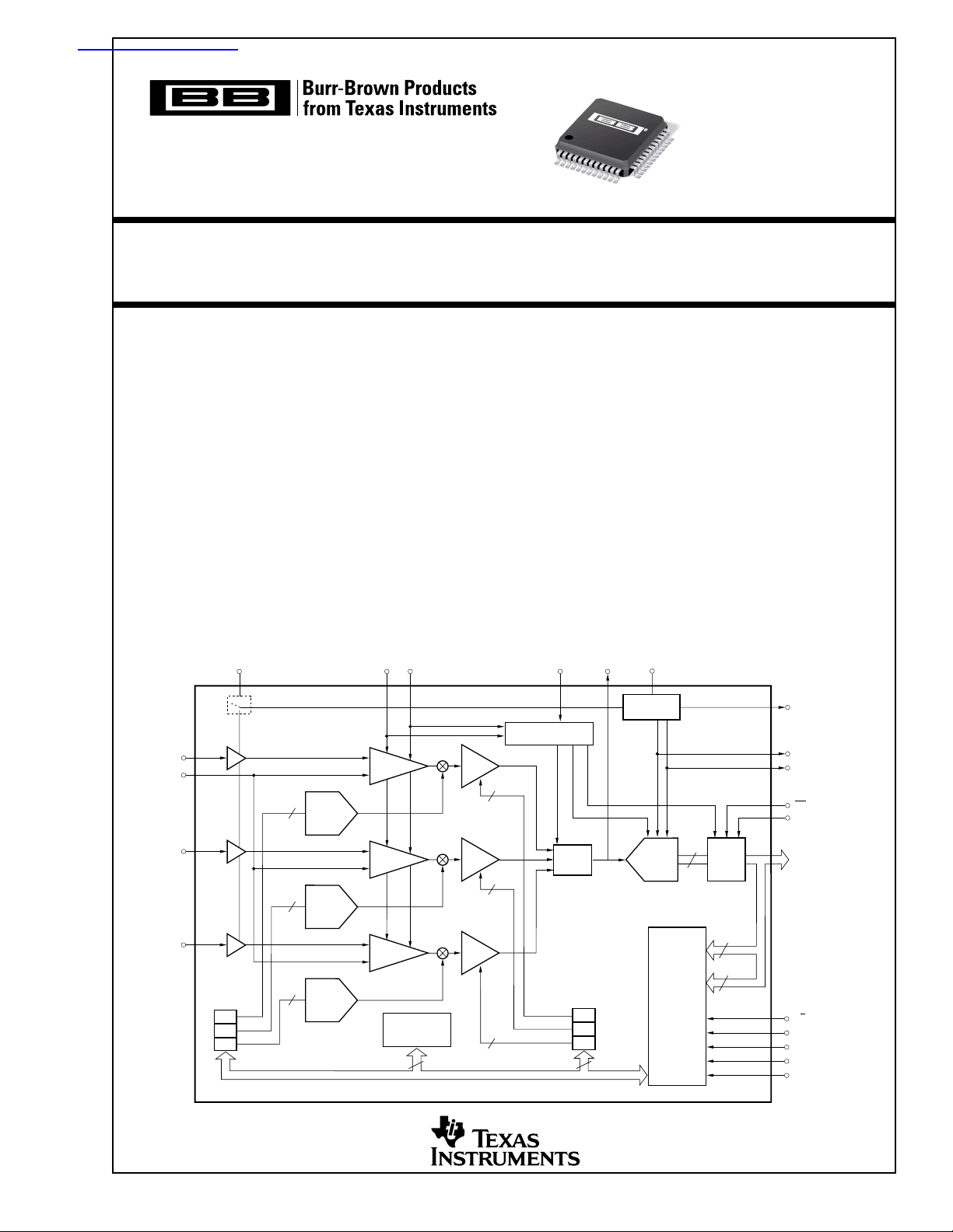
VSP3200
www.ti.com
CCD SIGNAL PROCESSOR FOR
SCANNER APPLICATIONS
FEATURES
F INTEGRATED TRIPLE-CORRELATED
DOUBLE SAMPLER
F OPERATION MODE SELECTABLE:
1-Channel, 3-Channel CCD Mode, 8Msps
F PROGRAMMABLE GAIN AMPLIFIER:
0dB to +13dB
F SELECTABLE OUTPUT MODES:
Normal/Demultiplexed
F OFFSET CONTROL RANGE: ±500mV
F +3V, +5V Digital Output
F LOW POWER: 300mW (typ)
F LQFP-48 SURFACE-MOUNT PACKAGE
VSP3200
VSP3210
DESCRIPTION
The VSP3200 and VSP3210 are complete CCD image
processors that operate from single +5V supplies.
This complete image processor includes three Correlated Double Samplers (CDSs) and Programmable
Gain Amplifiers (PGAs) to process CCD signals.
The VSP3200 is interface compatible with the
VSP3210, which is a 16-bit, one-chip product.
The VSP3210 is pin-to-pin compatible with VSP3100,
when in demultiplexed output mode.
The VSP3200 and VSP3210 can be operated from 0°C
to +85°C, and are available in LQFP-48 packages.
RINP
AGND
GINP
BINP
Clamp
Clamp
Clamp
Register
Offset
R
G
B
CK1CLP CK2
CDS
10
10-Bit
DAC
CDS
10
10-Bit
DAC
CDS
10
10-Bit
DAC
Configuration
Register
PGA
6
PGA
6
PGA
6
VSP3200
ADCCK
Timing Generator
MUX
Control
Register
Gain
R
G
B
68
TP0
V
REF
Reference
Circuit
16-Bit
A/D
Converter
Register
Port
CM
REFP
REFN
OE
V
DRV
Digital
Output
Control
16
3
10
B0-B15
(A0-A2, D0-D9)
P/S
WRT
RD
SCLK
SD
Copyright © 2000, Texas Instruments Incorporated SBMS012A Printed in U.S.A. November, 2000
SPECIFICATIONS
At TA = 25°C, VCC = +5.0V, V
otherwise specified.
PARAMETER CONDITIONS MIN TYP MAX UNITS
RESOLUTION 16 Bits
CONVERSION CHARACTERISTICS
1-Channel CCD Mode, Max 8 MHz
3-Channel CCD Mode, Max 8 MHz
DIGITAL INPUTS
Logic Family CMOS
Convert Command Start Conversion Rising Edge of ADCCK Clock
High-Level Input Current (V
Low-Level Input Current (VIN = 0V) 20 µA
Positive-Going Threshold Voltage 2.20 V
Negative-Going Threshold Voltage 0.80 V
Input Limit AGND – 0.3 V
Input Capacitance 5pF
ANALOG INPUTS
Full-Scale Input Range 0.5 3.5 Vp-p
Input Capacitance 10 pF
Input Limits AGND – 0.3 V
External Reference Voltage Range 0.25 1.75 V
Reference Input Resistance 800 W
DYNAMIC CHARACTERISTICS
Integral Non-Linearity (INL) V
Differential Non-Linearity (DNL) ±1.5 LSB
No Missing Codes
Output Noise 8.0 LSBs rms
PSRR V
DC ACCURACY
Zero Error 0.8 % FS
Gain Error 1.5 % FS
Offset Control Range 10-Bit Control DAC
DIGITAL OUTPUTS
Logic Family CMOS
Logic Coding Straight Binary
Digital Data Output Rate, Max Normal Mode 8 MHz
Supply Range +2.7 +5.3 V
V
DRV
Output Voltage, V
DRV
Low Level I
High Level IOH = 50µA +4.6 V
Low Level I
High Level I
Output Voltage, V
DRV
Low Level I
High Level I
Output Enable Time Output Enable = LOW 20 40 ns
3-State Enable Time Output Enable = HIGH 2 10 ns
Output Capacitance 5pF
Data Latency 8 Clock Cycles
Data Output Delay C
POWER-SUPPLY REQUIREMENTS
Supply Voltage: V
CC
Supply Current: ICC (No Load) 3-Ch CCD Mode 70 mA
Power Dissipation (No Load) 3-Ch CCD Mode 350 mW
TEMPERATURE RANGE
Operation Temperature LQFP-48 0 +85 °C
Thermal Resistance
= +3.0V, Conversion Rate (f
DRV
ADCCK
) = 6MHz, f
= 2MHz, f
CK1
= 2MHz, PGA Gain = 1, normal output mode, no output load, unless
CK2
VSP3200Y
VSP3210Y
= VCC) 20 µA
IN
+ 0.3 V
CC
+ 0.3 V
CC
= 500mV (V
IN
PGA Gain = 0dB, Input Grounded
= +5V, ±0.25V 0.04 % FSR
CC
= 1.0V) ±8 LSB
REF
Guaranteed
Output Voltage Range ±500 mV
Demultiplexed Mode 8 MHz
= +5V
= 50µA +0.1 V
OL
= 1.6mA +0.4 V
OL
= 0.5mA +2.4 V
OH
= +3V
= 50µA +0.1 V
OL
= 50µA +2.5 V
OH
= 15pF 12 ns
L
4.7 5 5.3 V
1-Ch CCD Mode 60 mA
1-Ch CCD Mode 300 mW
θ
JA
100 °C/W
2
VSP3200, 3210
SBMS012A
ABSOLUTE MAXIMUM RATINGS
, V
Supply Voltage: V
Supply Voltage Differences: Among V
GND Voltage Differences: Among GNDA........................................ ±0.1V
Digital Input Voltage ............................................... –0.3V to (V
Analog Input Voltage .............................................. –0.3V to (V
Input Current (Any Pins Except Supplies) .....................................±10mA
Ambient Temperature Under Bias ................................. –40°C to +125°C
Storage Temperature .................................................... –55°C to +125°C
Junction Temperature.................................................................... +150°C
Lead Temperature (soldering, 5s)................................................. +260°C
Package Temperature (IR Reflow, peak, 10s) ............................. +235°C
NOTE: (1) Stresses above these ratings may cause permanent damage.
Exposure to absolute maximum conditions for extended periods may degrade
device reliability.
...............................................................+6.5V
CC
DRV
(1)
.........................................±0.1V
CC
CC
CC
+ 0.3V)
+ 0.3V)
ELECTROSTATIC
DISCHARGE SENSITIVITY
This integrated circuit can be damaged by ESD. Burr-Brown
recommends that all integrated circuits be handled with
appropriate precautions. Failure to observe proper handling
and installation procedures can cause damage.
ESD damage can range from subtle performance degradation
to complete device failure. Precision integrated circuits may
be more susceptible to damage because very small parametric
changes could cause the device not to meet its published
specifications.
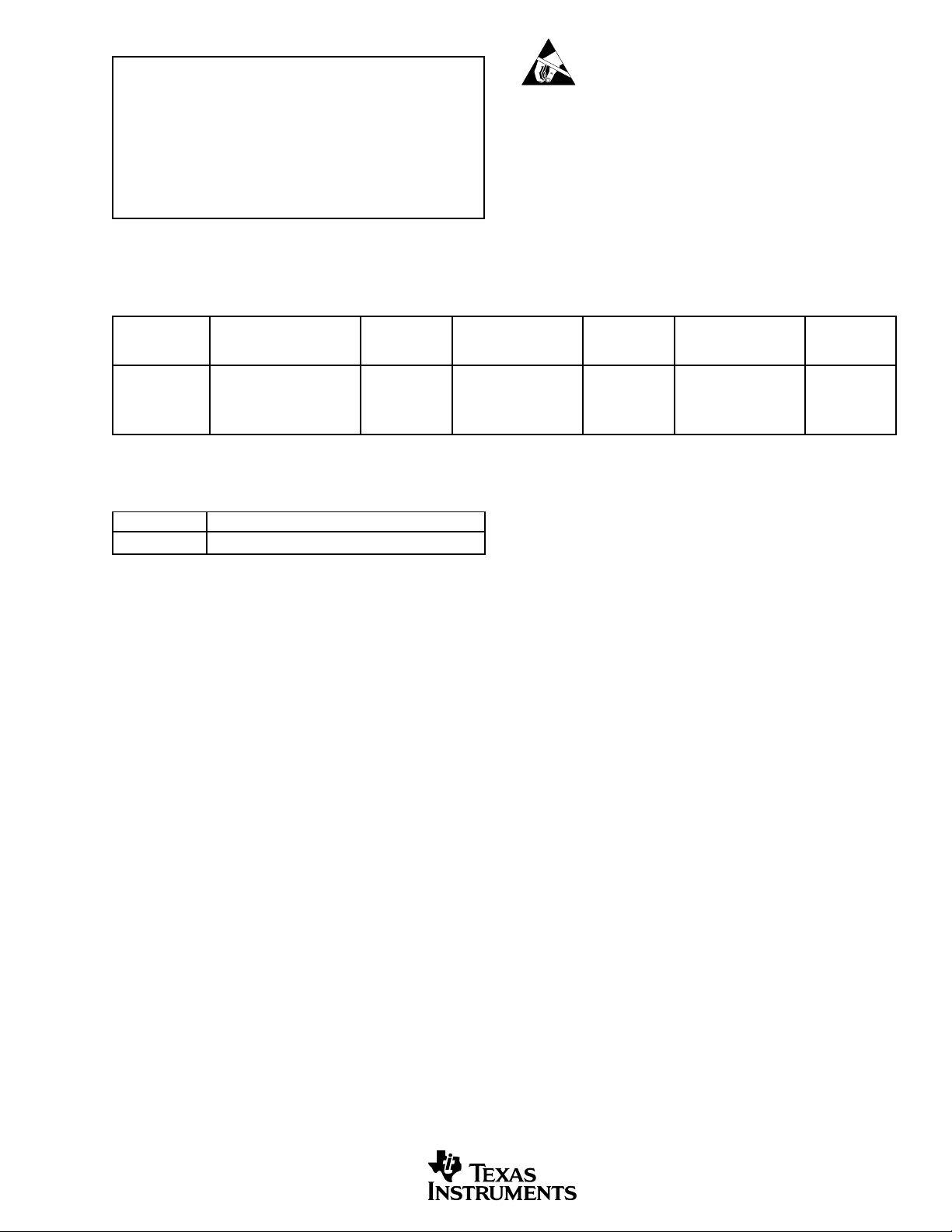
PACKAGE/ORDERING INFORMATION
PACKAGE SPECIFIED
PRODUCT PACKAGE NUMBER RANGE MARKING NUMBER
DRAWING TEMPERATURE PACKAGE ORDERING TRANSPORT
VSP3200Y LQFP-48 340 0°C to +85°C VSP3200Y VSP3200Y 250-Piece Tray
"""""VSP3200Y/2K Tape and Reel
VSP3210Y LQFP-48 340 0°C to +85°C VSP3210Y VSP3210Y 250-Piece Tray
"""""VSP3210Y/2K Tape and Reel
NOTE: (1) Models with a slash (/) are available only in Tape and Reel in the quantities indicated (e.g., /2K indicates 2000 devices per reel). Ordering 2000 pieces
of “VSP3200Y/2K” will get a single 2000-piece Tape and Reel.
(1)
MEDIA
DEMO BOARD ORDERING INFORMATION
PRODUCT PACKAGE
VSP3200Y DEM-VSP3200Y
VSP3200, 3210
SBMS012A
3
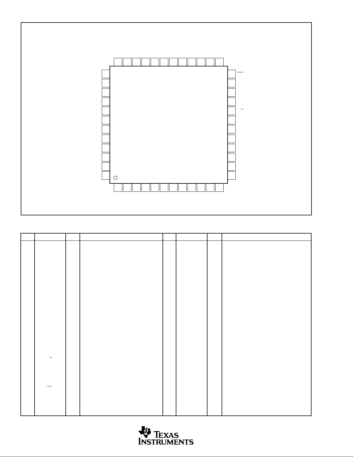
PIN CONFIGURATION
Top View LQFP
B11 (A1)
B10 (A0)
B9 (D9)
B8 (D8)
B7 (D7)
B6 (D6)
B5 (D5)
B4 (D4)
B3 (D3)
B2 (D2)
B1 (D1)
B0 (D0) LSB
36 35 34 33 32 31 30
29 28 27 26
B13
B14
V
DRV
V
V
AGND
TP0
V
REF
V
REFN
37
38
39
40
41
42
CC
43
CC
44
45
46
47
CC
48
B12 (A2)
B15 (MSB)
12345678910112512
CM
REFP
AGND
AGND
PIN DESCRIPTIONS (VSP3200Y)
PIN DESIGNATOR TYPE DESCRIPTION
1 CM AO Common-Mode Voltage
2 REFP AO Upper-Level Reference
3 AGND P Analog Ground
4 AGND P Analog Ground
5 RINP AI Red Channel Analog Input
6 AGND P Analog Ground
7 GINP AI Green Channel Analog Input
8 AGND P Analog Ground
9 BINP AI Blue Channel Analog Input
10 AGND P Analog Ground
11 V
12 CLP DI Clamp Enable
13 V
14 ADCCK DI Clock for A/D Converter Digital Data Output
CC
CC
15 CK1 DI Sample Reference Clock
16 CK2 DI Sample Data Clock
17 AGND P Analog Ground
18 RD DI Read Signal for Registers
19 WRT DI Write Signal for Registers
20 P/S DI Parallel/Serial Port Select
21 SD DI Serial Data Input
22 SCLK DI Serial Data Shift Clock
23 V
24 OE DI Output Enable
CC
25 B0 (D0) LSB DIO A/D Output (Bit 0) and Register Data (D0)
26 B1 (D1) DIO A/D Output (Bit 1) and Register Data (D1)
27 B2 (D2) DIO A/D Output (Bit 2) and Register Data (D2)
28 B3 (D3) DIO A/D Output (Bit 3) and Register Data (D3)
P Analog Power Supply, +5V
HIGH = Enable, LOW = Disable
P Analog Power Supply, +5V
HIGH = Parallel Port, LOW = Serial Port
P Analog Power Supply, +5V
24
OE
23
V
CC
22
SCLK
21
SD
20
P/S
19
WRT
VSP3200Y
RINP
AGND
GINP
AGND
BINP
AGND
18
RD
17
AGND
16
CK2
15
CK1
14
ADCCK
13
V
CC
CC
V
CLP
PIN DESIGNATOR TYPE DESCRIPTION
29 B4 (D4) DIO A/D Output (Bit 4) and Register Data (D4)
30 B5 (D5) DIO A/D Output (Bit 5) and Register Data (D5)
31 B6 (D6) DIO A/D Output (Bit 6) and Register Data (D6)
32 B7 (D7) DIO A/D Output (Bit 7) and Register Data (D7)
33 B8 (D8) DIO A/D Output (Bit 8) and Register Data (D8)
B0 LSB DO A/D Output (Bit 0) when Demultiplexed Output Mode
34 B9 (D9) DIO A/D Output (Bit 9) and Register Data (D9)
B1 DO A/D Output (Bit 1) when Demultiplexed Output Mode
35 B10 (A0) DIO A/D Output (Bit 10) and Register Address (A0)
B2 DO A/D Output (Bit 2) when Demultiplexed Output Mode
36 B11 (A1) DIO A/D Output (Bit 11) and Register Address (A1)
B3 DO A/D Output (Bit 3) when Demultiplexed Output Mode
37 B12 (A2) DIO A/D Output (Bit 12) and Register Address (A2)
B4 DO A/D Output (Bit 4) when Demultiplexed Output Mode
38 B13 DO A/D Output (Bit 13)
B5 DO A/D Output (Bit 5) when Demultiplexed Output Mode
39 B14 DO A/D Output (Bit 14)
B6 DO A/D Output (Bit 6) when Demultiplexed Output Mode
40 B15 MSB DO A/D Output (Bit 15)
B7 MSB DO A/D Output (Bit 7) when Demultiplexed Output Mode
41 V
42 V
43 V
44 AGND P Analog Ground
DRV
CC
CC
P Digital Output Driver Power Supply
P Analog Power Supply, +5V
P Analog Power Supply, +5V
45 TP0 AO A/D Converter Input Monitor Pin (single-ended output)
46 V
REF
AIO Reference Voltage Input/Output
INT Ref: Bypass to GND with 0.1µF
EXT Ref: Input Pin for Ref Voltage
47 V
48 REFN AO Lower-Level Reference
CC
P Analog Power Supply, +5V
4
VSP3200, 3210
SBMS012A
PIN CONFIGURATION
Top View LQFP
B5, B13
B4, B12
B3, B11
B2, B10
B1, B9
B0, B8 (LSB)NCNC
36 35 34 33 32 31 30
NC
NC
29 28 27 26
NC
NC
NC
NC
V
DRV
V
V
AGND
TP0
V
REF
V
REFN
37
38
39
40
41
42
CC
43
CC
44
45
46
47
CC
48
B6, B14
B7, B15 (MSB)
12345678910112512
CM
REFP
AGND
PIN DESCRIPTIONS (VSP3210Y)
PIN DESIGNATOR TYPE DESCRIPTION
1 CM AO Common-Mode Voltage
2 REFP AO Upper-Level Reference
3 AGND P Analog Ground
4 AGND P Analog Ground
5 RINP AI Red Channel Analog Input
6 AGND P Analog Ground
7 GINP AI Green Channel Analog Input
8 AGND P Analog Ground
9 BINP AI Blue Channel Analog Input
10 AGND P Analog Ground
11 V
12 CLP DI Clamp Enable
13 V
14 ADCCK DI Clock for A/D Converter Digital Data Output
CC
CC
15 CK1 DI Sample Reference Clock
16 CK2 DI Sample Data Clock
17 AGND P Analog Ground
18 AGND P Analog Ground
19 WRT DI Write Signal for Registers
20 AGND P Analog Ground
21 SD DI Serial Data Input
22 SCLK DI Serial Data Shift Clock
23 V
24 OE DI Output Enable
CC
25 NC – Should Be Left OPEN
26 NC – Should Be Left OPEN
27 NC – Should Be Left OPEN
28 NC – Should Be Left OPEN
29 NC – Should Be Left OPEN
P Analog Power Supply, +5V
HIGH = Enable, LOW = Disable
P Analog Power Supply, +5V
P Analog Power Supply, +5V
24
OE
23
V
CC
22
SCLK
21
SD
20
AGND
19
WRT
VSP3210Y
RINP
AGND
AGND
GINP
AGND
BINP
V
AGND
18
AGND
17
AGND
16
CK2
15
CK1
14
ADCCK
13
V
CC
CC
CLP
PIN DESIGNATOR TYPE DESCRIPTION
30 NC – Should Be Left OPEN
31 B0 LSB DO A/D Output (Bit 0) LSB
B8 DO A/D Output (Bit 8)
32 B1 DO A/D Output (Bit 1)
B9 DO A/D Output (Bit 9)
33 B2 DO A/D Output (Bit 2)
B10 DO A/D Output (Bit 10)
34 B3 DO A/D Output (Bit 3)
B11 DO A/D Output (Bit 11)
35 B4 DO A/D Output (Bit 4)
B12 DO A/D Output (Bit 12)
36 B5 DO A/D Output (Bit 5)
B13 DO A/D Output (Bit 13)
37 B6 DO A/D Output (Bit 6)
B14 DO A/D Output (Bit 14)
38 B7 DO A/D Output (Bit 7)
B15 MSB DO A/D Output (Bit 15) MSB
39 NC – Should Be Left OPEN
40 NC – Should Be Left OPEN
41 V
42 V
43 V
44 AGND P Analog Ground
DRV
CC
CC
P Digital Output Driver Power Supply
P Analog Power Supply, +5V
P Analog Power Supply, +5V
45 TP0 AO A/D Converter Input Monitor Pin (single-ended output)
46 V
REF
AIO Reference Voltage Input/Output
INT Ref: Bypass to GND with 0.1µF
EXT Ref: Input Pin for Ref Voltage
47 V
48 REFN AO Lower-Level Reference
CC
P Analog Power Supply, +5V
VSP3200, 3210
SBMS012A
5

TIMING SPECIFICATIONS
VSP3200 AND VSP3210 1-CHANNEL CCD MODE TIMING
Pixel 1
Pixel 2
CCD Output
t
S
t
CK1W-1
t
S
t
CK1P-1
CK1
t
t
CK1CK2-1
CK2W-1
t
CK2CK1-1
CK2
t
CNV
ADCCK
t
t
SET
CK1ADC
t
ADCCK2-1
Pixel 1
t
ADCW
t
ADCP
t
ADCW
SYMBOL PARAMETER MIN TYP MAX UNITS
t
CK1W-1
t
CK1P-1
t
CK2W-1
t
CK1CK2-1
t
CK2CK1-1
t
CK1ADC
t
ADCCK2-1
t
ADCW
t
ADCP
t
S
t
SET
t
CNV
DL Data Latency, Normal Operation Mode 8 (fixed) Clock Cycles
CK1 Pulse Width 20 ns
1-Channel Mode Conversion Rate 125 166 ns
CK2 Pulse Width 20 ns
CK1 Falling to CK2 Rising 15 ns
CK2 Falling to CK1 Rising 50 ns
CK1 Rising to ADCCK Falling 10 ns
ADCCK Falling to CK2 Falling 15 ns
ADCCK Pulse Width 62 83 ns
ADCCK Period 125 166 ns
Sampling Delay 10 ns
ADCCK Rising to CK1 Rising 40 ns
Conversion Delay 10 ns
VSP3200 TIMING FOR PARALLEL PORT READING
P/S
Register Data
A2-A0
RD
D9-D0
SYMBOL
Parallel Ready Time 20 ns
t
PR
t
DA
t
RW
t
RD
t
RH
Data Setup Time 30 50 ns
Address Setup Time 20 50 ns
NOTES: (1) This feature is for the VSP3200 only. (2) Reading out register
data through the serial port is prohibited.
t
PR
Valid
t
DA
Stable
t
RW
t
RD
Valid
PARAMETER MIN TYP MAX UNITS
Read Out Delay 20 ns
Data Hold Time 1 ns
t
RH
VSP3200 TIMING FOR PARALLEL PORT WRITING
P/S
A2-A0
D9-D0
WRT
Register Data
SYMBOL
t
t
t
t
Parallel Ready Time 20 ns
PR
t
W
WD
Address Setup Time 20 50 ns
RW
DA
NOTE: (1) This feature is for the VSP3200 only.
t
PR
Stable
t
RW
Stable
t
DAtW
t
WD
Valid
PARAMETER MIN TYP MAX UNITS
WRT Pulse Width 30 50 ns
Data Valid Time 30 ns
Data Setup Time 30 50 ns
6
VSP3200, 3210
SBMS012A

VSP3200 AND VSP 3210 3-CHANNEL CCD MODE TIMING
Pixel 1 (R/G/B) Pixel 2 (R/G/B)
CCD Output
t
S
t
CK1W-3
CK1
t
CK1CK2-3
t
ADCCK2-3
CK2
ADCCK
t
SET
t
t
CNV
S
t
CK2W-3
t
CK1P-3
t
CK2CK1-3
t
SET
ADCW
(G)
(B) Pixel 1 (R)
Pixel 1 (G) Pixel 1 (B)
(R)
t
ADCW
t
ADCP
t
SYMBOL PARAMETER MIN TYP MAX UNITS
t
CK1W-3
t
CK1P-3
t
CK2W-3
t
CK1CK2-3
t
CK2CK1-3
t
ADCCK2-3
t
ADCW
t
ADCP
t
S
t
SET
t
CNV
DL Data Latency, Normal Operation Mode 8 (fixed) Clock Cycles
CK1 Pulse Width 20 ns
3-Channel Mode Conversion Rate 375 500 ns
CK2 Pulse Width 20 ns
CK1 Falling to CK2 Rising 15 ns
CK2 Falling to CK1 Rising 112 ns
ADCCK Falling to CK2 Falling 5 n s
ADCCK Pulse Width 62 83 ns
ADCCK Period 125 166 ns
Sampling Delay 10 n s
ADCCK Rising to CK1 Rising 10 ns
Conversion Delay 40 ns
VSP3200, 3210
SBMS012A
7

DIGITAL DATA OUTPUT SEQUENCE: 1-Ch CCD Mode, (B-Ch: D4 = 1 and D5 = 0)
Pixel (n+1) Pixel (n+8)
• • •
• • •
t
SET
t
CNV
(n) (n+1) (n+7) (n+8)
B (n)
t
CNV
B (n+1) B (n+7) B (n+8)
• • •
• • •
• • •
• • •
CCD Output
CK1
CK2
ADCCK
CDS Output
A/D Input
Digital Output (Normal Mode)
t
SET
Pixel (n)
DIGITAL DATA OUTPUT SEQUENCE: 3-Ch CCD Mode, R > G > B Sequence
B (n)
CCD Output
CK1
CK2
ADCCK
CDS Output
A/D Input
Digital Output
(Normal Mode)
Pixel (n)
Pixel (n+1) Pixel (n+2)
t
SET
t
CNV
(n)
R (n) G (n) B (n)
R (n+1) G (n+1) B (n+1) R (n+2)
t
SET
t
CNV
(n+1) (n+2)
R (n) G (n) B (n)
R (n+1)
8
VSP3200, 3210
SBMS012A
VSP3200 AND VSP3210 TIMING FOR DIGITAL DATA OUTPUT (DEMULTIPLEXED OUTPUT MODE)
VSP3200 TIMING FOR DIGITAL DATA OUTPUT
(NORMAL OUTPUT MODE)
(1)
P/S
t
OES
OE
t
OER
ADCCK
Digital Output
B[15:0]
SYMBOL
t
OES
t
OER
t
3E
t
OEW
t
DODH
t
DODL
t
OEP
Digital Data Output Delay, High-Byte
Digital Data Output Delay, Low-Byte
t
DODH
(Hi-Z)
PARAMETER MIN TYP MAX UNITS
A/D Output Enable Setup Time
Output Enable Time 20 40 ns
3-State Enable Time 2 10 ns
OE Pulse Width 100 ns
Parallel Port Setup Time 10 ns
NOTES: (1) The VSP3210 has no P/S signal; t
not needed. (2) When in inhibit operation mode, OE sets LOW during
t
OEW
(n)
t
DODL
n (B6-B13)
(n)
t
DODH
n (B0-B5)
20 ns
OES
(n+1)
n+1 (B6-B13)
and t
t
OEP
t
3E
12 ns
12 ns
specs. are
OEP
(Hi-Z)
P/S = HIGH period.
VSP3200 AND VSP3210 TIMING FOR SERIAL PORT
WRITING
P/S
t
OES
t
OEW
t
OEP
OE
ADCCK
Digital Output
B[15:0]
t
DOD
t
OER
t
DOD
Data n (14-Bit)
t
DOD
Data n+1
(n+2) (n+1) (n)
Data n+2
t
3E
(Hi-Z)(Hi-Z)
SYMBOL PARAMETER MIN TYP MAX UNITS
A/D Output Enable Setup Time 20 ns
t
OES
t
OER
t
t
OEW
t
DOD
t
OEP
3E
Output Enable Time 20 40 ns
3-State Enable Time 2 10 ns
OE Pulse Width 100 ns
Digital Data Output Delay 12 ns
Parallel Port Setup Time 10 ns
NOTES: (1) This feature is for the VSP3200 only. (2) When in inhibit
operation mode, OE sets LOW during P/S = HIGH period.
(1)
P/S
SCLK
SD
WRT
Register Data
SYMBOL
t
W
t
WD
t
SD
t
SCK
t
SCKP
t
SS
t
SW
t
SS
t
SD
A2 A1
A0 D9 D1 D0
PARAMETER MIN TYP MAX UNITS
WRT Pulse Width 30 50 ns
Data Valid Time 30 ns
Data Ready Time 15 50 ns
Serial Clock Pulse Width
Serial Clock Period 60 100 ns
Serial Ready 100 200 ns
WRT Pulse Setup Time 50 ns
t
SCKtSCK
t
SCKP
• • •
t
SW
30 50 ns
NOTE: (1) VSP3210 has no P/S signal; tSS spec. is not needed.
t
W
t
WD
Valid
VSP3200, 3210
SBMS012A
9

THEORY OF OPERATION
INTRODUCTION
The VSP3200 and VSP3210 are complete mixed-signal ICs
that contain all of the key features associated with the
processing of the CCD line sensor output signal in scanners,
photo copiers, and similar applications. See the simplified
block diagram on page 1 for details. The VSP3200 and
VSP3210 include Correlated Double Samplers (CDSs), Programmable Gain Amplifiers (PGAs), Multiplexer (MUX),
Analog-to-Digital (A/D) converter, input clamp, offset control, serial interface, timing control, and reference control
generator.
The VSP3200 and VSP3210 can be operated in one of the
following two modes:
• 1-Channel CCD mode
• 3-Channel CCD mode
1-CHANNEL CCD MODE
In this mode, the VSP3200 and VSP3210 process only one
CCD signal (D3 of the Configuration Register sets to “1”).
The CCD signal is AC-coupled to RINP, GINP, or BINP
(depending on D4 and D5 of the Configuration Register). The
CLP signal enables internal biasing circuitry to clamp this
input to a proper voltage, so that internal CDS circuitry can
work properly. The VSP3200 and VSP3210 inputs may be
applied as DC-coupled inputs, which needs to be level-shifted
to a proper DC level.
The CDS takes two samples of the incoming CCD signals:
the CCD reset signal is taken on the falling edge of CK1, and
the CCD information is taken on the falling edge of CK2.
These two samples are then subtracted by the CDS and the
result is stored as a CDS output.
In the 1-Channel CCD mode, only one of the three channels
is enabled. Each channel consists of a 10-bit offset Digital-toAnalog Converter (DAC) with a range from –500mV to
+500mV. A 3-to-1 analog MUX is inserted between the CDSs
and a high-performance, 16-bit A/D converter. The outputs of
the CDSs are then multiplexed to the A/D converter for
digitization. The analog MUX is not cycling between channels
in this mode. Instead, it is connected to a specific channel,
depending on the contents of D4 and D5 in the Configuration
Register.
The VSP3200 allows two types of output modes:
• Normal (D7 of Configuration Register sets to “0”).
• Demultiplexed (D7 of Configuration Register sets to “1”).
The VSP3210 allows one type of output mode:
• Demultiplexed (D7 of Configuration Register sets to “1”).
As specified in the “1-Channel CCD Mode” timing diagram,
the rising edge of CK1 must be in the HIGH period of
ADCCK, and at the same time, the falling edge of the CK2
must be in the LOW period of ADCCK. Otherwise, the
VSP3200 and VSP3210 will not function properly.
3-CHANNEL CCD MODE
In the 3-Channel CCD mode, the VSP3200 and VSP3210 can
simultaneously process triple output CCD signals. CCD signals are AC coupled to the RINP, GINP, and BINP inputs. The
CLP signal enables internal biasing circuitry to clamp these
inputs to a proper voltage so that internal CDS circuitry can
work properly. The VSP3200 and VSP3210 inputs may be
applied as DC-coupled inputs, which need to be level-shifted
to a proper DC level.
The CDSs take two samples of the incoming CCD signals:
the CCD reset signals are taken on the falling edge of CK1,
and the CCD information is taken on the falling edge of
CK2. These two samples are then subtracted by the CDSs
and the results are stored as a CDS output.
In this mode, three CDSs are used to process three inputs
simultaneously. Each channel consists of a 10-bit Offset
DAC (range from –500mV to +500mV). A 3-to-1 analog
MUX is inserted between the CDSs and a high-performance,
16-bit A/D converter. The outputs of the CDSs are then
multiplexed to the A/D converter for digitization. The analog MUX is switched at the falling edge of CK2, and can be
programmed to cycle between the Red, Green, and Blue
channels. When D6 of the Configuration Register sets to
“0”, the MUX sequence is Red > Green > Blue. When D6
of the Configuration Register sets to “1”, the MUX sequence
is Blue > Green > Red.
MUX resets at the falling edge of CK1. In the case of a
Red > Green > Blue sequence, it resets to “R”, and in the
case of a Blue > Green > Red sequence, it resets to “B”.
The VSP3200 allows two types of output modes:
• Normal (D7 of Configuration Register sets to “0”).
• Demultiplexed (D7 of Configuration Register sets to “1”).
The VSP3210 allows one type of output mode:
• Demultiplexed (D7 of Configuration Register sets to “1”).
As specified in the “3-Channel CCD Mode” timing diagram,
the falling edge of CK2 must be in the LOW period of
ADCCK. If the falling edge of CK2 is in the HIGH period
of ADCCK (in the timing diagram, ADCCK for sampling
B-channel), the VSP3200 and VSP3210 will not function
properly.
DIGITAL OUTPUT FORMAT
See Table I for the Digital Output Format. The VSP3200 and
VSP3210 can be operated in one of the following two digital
output modes:
• Normal output.
• Demultiplexed (B15-based Big Endian Format).
In Normal mode, the VSP3200 outputs the 16-bit data by B0
(pin 25) through B15 (pin 40) simultaneously.
In Demultiplexed mode, the VSP3200 outputs the high byte
(upper 8 bits) by B8 (pin 33) through B15 (pin 40) at the
rising edge of ADCCK HIGH, then outputs the low byte
(lower 8 bits) by B8 (pin 33) through B15 (pin 40) at the
falling edge of ADCCK.
10
VSP3200, 3210
SBMS012A

The VSP3210 can be operated in Demultiplexed mode as the
digital output (B13-based Big Endian Format), as shown in
Table I. The VSP3210 outputs the high byte (upper 8 bits)
by pin 31 through pin 38 at the rising edge of ADCCK
HIGH, then outputs the low byte (lower 8 bits) by pin 31
through pin 38 at the falling edge of ADCCK (as shown in
Table II). An 8-bit interface can be used between the
VSP3200 and the Digital Signal Processor, allowing for a
low-cost system solution.
VSP3200 and VSP3210 from any digital noise activities on
the bus coupling back high-frequency noise. In addition,
resistors in series with each data line may help minimize the
surge current. Their use depends on the capacitive loading
seen by the converter. As the output levels change from
LOW to HIGH and HIGH to LOW, values in the range of
100W to 200W will limit the instantaneous current the output
stage has to provide for recharging the parasitic capacitances.
DIGITAL OUTPUTS
The digital outputs of the VSP3200 and VSP3210 are
designed to be compatible with both high-speed TTL and
CMOS logic families. The driver stage of the digital outputs
is supplied through a separate supply pin, V
(pin 41),
DRV
which is not connected to the analog supply pins (VCC). By
adjusting the voltage on V
, the digital output levels will
DRV
vary respectively. Thus, it is possible to operate the VSP3200
and VSP3210 on +5V analog supplies while interfacing the
digital outputs to 3V logic. It is recommended to keep the
capacitive loading on the data lines as low as possible
(typically less than 15pF). Larger capacitive loads demanding higher charging current surges can feed back to the
analog portion of the VSP3200 and VSP3210 and influence
the performance. If necessary, external buffers or latches
may be used, providing the added benefit of isolating the
PROGRAMMABLE GAIN AMPLIFIER (PGA)
The VSP3200 and VSP3210 have one PGA which is inserted between the CDSs and the 3:1 MUX. The PGA is
controlled by a 6-bit of Gain Register; each channel (Red,
Green, and Blue) has its own Gain Register.
The gain varies from 1 to 4.8 (0dB to 14dB), and the curve
has log characteristics. Gain Register Code all “0” corresponds to minimum gain, and Code all “1” corresponds to
maximum gain.
The transfer function of the PGA is:
Gain = 80/(80 – GC)
where, GC is the integer representation of the 6-bit PGA
gain register.
Figure 1 shows the PGA transfer function plots.
PIN 40 39 38 37 36 35 34 33 32 31 30 29 28 27 26 25
High Byte B15 B14 B13 B13 B11 B10 B9 B8 Low Low Low Low Low Low Low Low
Low Byte B7 B6 B5 B4 B3 B2 B1 B0 Low Low Low Low Low Low Low Low
TABLE I. Output Format for VSP3200 (Demultiplexed Mode).
PIN 40 39 38 37 36 35 34 33 32 31 30 29 28 27 26 25
High Byte ––B15 B14 B13 B12 B11 B10 B9 B8 –– ––– –
Low Byte ––B7 B6 B5 B4 B3 B2 B1 B0 –– ––– –
TABLE II. Output Format for VSP3210.
5
4.5
4
3.5
3
Gain
2.5
2
1.5
1
0
4
8
12162024283236404448525660
PGA Gain Code (0 to 3)
FIGURE 1. PGA Transfer Function Plots.
VSP3200, 3210
SBMS012A
14
12
10
8
6
Gain (dB)
4
2
0
0
4
8
12162024283236404448525660
PGA Gain Code (0 to 63)
11

INPUT CLAMP
The input clamp should be used for 1-Channel and 3-Channel
CCD mode, and enabled when both CLP and CK1 are set to
HIGH.
Bit Clamp: the input clamp is always enabled.
Line Clamp: enables during the dummy pixel interval at
every horizontal line, and disables during the effective pixel
interval.
Generally, “Bit Clamp” is used for many scanner applications, however “Line Clamp” is used instead of “Bit Clamp”
when the clamp noise is impressive.
CHOOSING THE AC INPUT COUPLING
CAPACITORS
The purpose of the Input Coupling Capacitor is to isolate the
DC offset of the CCD array from affecting the VSP3200 and
VSP3210 input circuitry. The internal clamping circuitry is
used to restore the necessary DC bias to make the VSP3200
and VSP3210 input circuitry functional. Internal clamp voltage, V
HIGH. V
V
CLAMP
Register set to “0”), and V
, is set when both the CLP pin and CK1 are set
CLAMP
is 2.5V if V
changes depending on the value of V
CLAMP
is set to 1V (D1 of the Configuration
REF
CLAMP
is 3V if V
REF
REF
is set to 1.5V
(D1 of the Configuration Register set to “1”).
There are many factors that decide what size of Input
Coupling Capacitor is needed. Those factors are CCD signal
swing, voltage difference between the Input Coupling Capacitor, leakage current of the VSP3200 and VSP3210 input
circuitry, and the time period of CK1.
Figure 2 shows the equivalent circuit of the VSP3200 and
VSP3210 inputs.
In this equivalent circuit, Input Coupling Capacitor CIN, and
Sampling Capacitor C1, are constructed as a capacitor divider
during CK1. For AC analysis, OP inputs are grounded.
Therefore, the sampling voltage, VS, during CK1 is:
VS = (CIN/(CIN + C1)) • V
IN
From the above equation, we know that a larger CIN makes
VS close to VIN. In other words, the input signal (VIN) will
not be attenuated if CIN is large.
However, there is a disadvantage of using a large C
take longer for the CLP signal to charge up CIN so that the
input circuitry of the VSP3200 and VSP3210 can work
properly.
CHOOSING C
MAX
AND C
MIN
As mentioned before, a large CIN is better if there is enough
time for the CLP signal to charge up CIN so that the input
circuitry of the VSP3200 and VSP3210 can work properly.
Typically, 0.01µF to 0.1µF of CIN can be used for most
.
cases.
In order to optimize CIN, the following two equations can be
used to calculate the maximum (C
) and minimum (C
MAX
values of CIN:
C
where t
= (t
MAX
is the time when both CK1 and CLP go HIGH,
CK1
• N)/[RSW • ln(VD/V
CK1
ERROR
and N is the number of black pixels; RSW is the switch
resistance of the VSP3200 and VSP3210 (typically, driver
impedance + 4kW); VD is the droop voltage of CIN; V
is the voltage difference between VS and V
CLAMP
IN
)]
.
: it will
MIN
ERROR
)
CK1
C
1
4pF
C
CLP
CK1
IN
C
4pF
CK2
V
CLAMP
V
IN
Op
Amp
2
FIGURE 2. Equivalent Circuit of VSP3200 and VSP3210
Inputs.
C
MIN
= (II/V
ERROR
) • t
where II is the leakage current of the VSP3200 and VSP3210
input circuitry (10nA is a typical number for this leakage
current); t is the clamp pulse period.
SETTING FOR FULL-SCALE INPUT RANGE
The input range of the internal 16-bit A/D converter can be
set in two ways:
• Internal reference: to set the internal reference mode, D2
of the configuration register must be set to “0” and the
reference voltage set through D1. The full-scale input
voltage setting is twice the reference voltage. When the
reference voltage is set at 1V (D1 = “0”), the full-scale
voltage is 2Vp-p. However, when the reference voltage is
set at 1.5V (D1 = “1”), the full-scale voltage is 3Vp-p. In
internal reference mode, V
GND with a 0.1µF capacitor. Do not use V
should be connected to
REF
voltages in
REF
12
VSP3200, 3210
SBMS012A

other system circuits, as it would affect the reference
voltage of the A/D converter and prevent proper A/D
conversion.
• External Reference: to set the external reference mode,
D2 of the configuration register must be set to “1”. In
external reference mode, V
operates as an analog
REF
voltage input pin. Inputting half the voltage necessary for
the full-scale voltage range (e.g.: 1.7V applied for a
necessary 3.4Vp-p input range), with a reference voltage
range from 0.25V to 1.75V, will create the full-scale
range. Thus, when V
be 0.5Vp-p, and when V
is 0.5V, the full-scale range will
REF
is 1.75V, the full-scale range
REF
will be 3.5Vp-p.
PROGRAMMING THE VSP3200 AND VSP3210
The VSP3200 and VSP3210 consist of three CCD channels
and a 16-bit A/D. Each channel (Red, Green, and Blue) has
its own 10-bit Offset and 6-bit Gain Adjustable Registers to
be programmed by the user. There is also an 8-bit Configuration Register, on-chip, to program the different operation
modes. Those registers are shown in Table III.
ADDRESS POWER-ON
A2 A1 A0 REGISTER DEFAULT VALUE
0 0 0 Configuration Register (8-bit) All “0s”
0 0 1 Red Channel Offset Register (10-bit) All “0s”
0 1 0 Green Channel Offset Register (10-bit) All “0s”
0 1 1 Blue Channel Offset Register (10-bit) All “0s”
1 0 0 Red Channel Gain Register (6-bit) All “0s”
1 0 1 Green Channel Gain Register (6-bit) All “0s”
1 1 0 Blue Channel Gain Register (6-bit) All “0s”
1 1 1 Reserved
TABLE III. On-Chip Registers.
These registers can be accessed by the following two programming modes:
• Parallel Programming Mode (VSP3200 only) using digital data output pins, with the data bus assigned as D0 to
D9 (pins 25 to 34), and the address bus as A0 to A2 (pins
35 to 37). It can be used for both reading and writing
operations. However, it cannot be used by the
Demultiplexed mode (when D7 of the Configuration
Register is set to “1”).
• Serial Programming Mode using a serial port, Serial Data
(SD), the Serial Shift Clock (SCLK), and Write Signal
(WRT) assigned.
It can be used only for writing operations; reading operations via the serial port are prohibited.
Table IV shows how to access these modes (VSP3200 only).
OE P/S MODE
0 0 Digital data output enabled, Serial mode enabled
0 1 Prohibit mode (can not set this mode)
1 0 Digital data output disabled, Serial mode enabled
1 1 Digital data output disabled, Parallel mode enabled
TABLE IV. Access Mode for Serial and Parallel Port
(VSP3200 Only).
CONFIGURATION REGISTER
The Configuration Register design is shown in Table V.
BIT LOGIC ‘0’ LOGIC ‘1’
D0 CCD mode CIS mode
D1 V
D2 Internal Reference External Reference
D3 3-channel Mode, 1-channel Mode,
D4, D5
D6 MUX Sequence MUX Sequence
(1)
D7
NOTE: (1) D7 of the configuration register should always be set to “1” for the
VSP3210. Power-on default value is “0”; initial write operation for “1” is also
needed for the VSP3210, when in power-on.
= 1V V
REF
D4 and D5 disabled D4 and D5 enabled
(disabled when 3-channel) D4 D5
Red > Green > Blue Blue > Green >Red
Normal output mode Demultiplexed output mode
=1.5V
REF
00
1-channel mode, Red channel
01
1-channel mode, Green channel
10
1-channel mode, Blue channel
TABLE V. Configuration Register Design.
Power-on default value is all “0s”, set to 3-Channel CCD
mode with 1V internal reference, R > G > B MUX sequence,
and normal output mode.
For reading/writing to the Configuration Register, the address will be A2 = “0”, A1 = “0”, and A0 = “0”.
For Example:
A 3-Channel CCD with internal reference V
= 1V (2V
REF
full-scale input), R > G > B sequence and normal output
mode will be D0 = “0”, D1 = “0”, D2 =“0”, D3 = “0”,
D4 = “x (don’t care)”, D5 = “x (don’t care)”, D6 = “0”, and
D7 = “0”.
For this example, bypass V
with an appropriate capacitor
REF
(e.g.:, 10µF to 0.1µF) when internal reference mode is used.
Another Example:
A 1-Channel CCD mode (Green channel) with an external
1.2V reference (2.4V full-scale input), Demultiplexed Output mode will be D0 = “0”, D1 = “x (don’t care)”, D2 = “1”,
D3 = “1”, D4 = “0”, D5 = “1”, D6 = “x (don’t care)”, and
D7 = “1”.
For this example, V
will be an input pin applied with 1.2V.
REF
VSP3200, 3210
SBMS012A
13

OFFSET REGISTER
Offset Registers control the analog offset input to channels
prior to the PGA. There is a 10-bit Offset Register on each
channel. The offset range varies from –500mV to +500mV.
The Offset Register uses a straight binary code. All “0s”
corresponds to –500mV, and all “1s” corresponds to +500mV
of the offset adjustment. The register code (200H) corresponds to 0mV of the offset adjustment. The Power-on
default value of the Offset Register is all ”0s”, so the offset
adjustment should be set to –500mV.
PGA GAIN REGISTER
PGA Gain Registers control the gain to channels prior to the
digitization by the A/D converter. There is a 6-bit PGA Gain
Register on each channel. The gain range varies from 1 to
4.8 (from 0dB to 13dB). The PGA Gain Register is a straight
binary code. All “0s” corresponds to an analog gain of 0dB,
and all “1s” corresponds to an analog gain of 13dB. PGA
Transfer function is log gain curve. Power-on default value
is all “0s”, so that it sets the gain of 0dB.
OFFSET AND GAIN CALIBRATION SEQUENCE
When the VSP3200 and VSP3210 are powered on, they will
be initialized as 3-Channel CCDs, 1V internal reference
mode (2V full-scale) with an analog gain of 1, and normal
output mode. This mode is commonly used for CCD scanner
applications. The calibration procedure is done at the very
beginning of the scan.
To calibrate the VSP3200, use the following procedures:
1) Set the VSP3200 to the proper mode.
2) Set Offset to 0mV (control code: 00
), and PGA gain to
H
1 (control code: 200H).
3) Scan dark line.
4) Calculate the pixel offsets according to the A/D Converter
output.
5) Readjust input Offset Registers.
6) Scan white line.
7) Calculate gain. It will be the A/D Converter full-scale
divided by the A/D Converter output when the white line
is scanned.
8) Set the Gain Register. If the A/D Converter output is not
close to full-scale, go back to item 3. Otherwise, the
calibration is done.
The calibration procedure is started at the very beginning of
the scan. Once calibration is done, registers on the VSP3200
will keep this information (offset and gain for each channel)
during the operation.
RECOMMENDATION FOR POWER SUPPLY,
GROUNDING, AND DEVICE DECOUPLING
The VSP3200 and VSP3210 incorporate a very-high precision, high-speed A/D converter and analog circuitry vulnerable to any extraneous noise from the rails, etc. Therefore, it
should be treated as an analog component and all supply
pins, except V
, should be powered by the only analog
DRV
supply in the system. This will ensure the most consistent
results, since digital power lines often carry high levels of
wideband noise that otherwise would be coupled into the
device and degrade the achievable performance.
Proper grounding, bypassing, short lead length, and the use
of ground planes are particularly important for high-frequency designs. Multilayer PC boards are recommended for
the best performance since they offer distinct advantages
such as minimization of ground impedance, separation of
signal layers by ground layers, etc.
It is recommended that all ground pins of the VSP3200 and
VSP3210 be joined together at the IC and connected only to
the analog ground of the system. The driver stage of the
digital outputs (B[15:0]) is supplied through a dedicated
supply pin, V
, and should be completely separated from
DRV
other supply pins with at least a ferrite bead. Keeping the
capacitive loading on the output data lines as low as possible
(typically less than 15pF) is also recommended. Larger
capacitive loads demand higher charging current surges that
can feed back into the analog portions of the VSP3200 and
VSP3210, affecting device performance. If possible, external buffers or latches should be used, providing the added
benefit of isolating the VSP3200 and VSP3210 from any
digital noise activity on the data lines.
In addition, resistors in series with each data line may help
minimize surge currents. Values in the range of 100W to
200W will limit the instantaneous current the output stage
requires from recharging parasitic capacitances as output
levels change from LOW to HIGH or HIGH to LOW. As the
result of the high operation speed, the converter also generates high-frequency current transients and noises that are fed
back into the supply and reference lines. This requires that
the supply and reference pins be sufficiently bypassed. In
most cases, 0.1µF ceramic chip capacitors are adequate in
decoupling reference pins. Supply pins should be decoupled
to the ground plane with a parallel combination of tantalum
(1µF to 22µF) and ceramic (0.1µF) capacitors. Decoupling
effectiveness largely depends upon the proximity to the
individual pins.
14
VSP3200, 3210
SBMS012A

MPQF102
®
PACKAGE DRAWING

IMPORTANT NOTICE
Texas Instruments Incorporated and its subsidiaries (TI) reserve the right to make corrections, modifications,
enhancements, improvements, and other changes to its products and services at any time and to discontinue
any product or service without notice. Customers should obtain the latest relevant information before placing
orders and should verify that such information is current and complete. All products are sold subject to TI’s terms
and conditions of sale supplied at the time of order acknowledgment.
TI warrants performance of its hardware products to the specifications applicable at the time of sale in
accordance with TI’s standard warranty . Testing and other quality control techniques are used to the extent TI
deems necessary to support this warranty . Except where mandated by government requirements, testing of all
parameters of each product is not necessarily performed.
TI assumes no liability for applications assistance or customer product design. Customers are responsible for
their products and applications using TI components. T o minimize the risks associated with customer products
and applications, customers should provide adequate design and operating safeguards.
TI does not warrant or represent that any license, either express or implied, is granted under any TI patent right,
copyright, mask work right, or other TI intellectual property right relating to any combination, machine, or process
in which TI products or services are used. Information published by TI regarding third–party products or services
does not constitute a license from TI to use such products or services or a warranty or endorsement thereof.
Use of such information may require a license from a third party under the patents or other intellectual property
of the third party , or a license from TI under the patents or other intellectual property of TI.
Reproduction of information in TI data books or data sheets is permissible only if reproduction is without
alteration and is accompanied by all associated warranties, conditions, limitations, and notices. Reproduction
of this information with alteration is an unfair and deceptive business practice. TI is not responsible or liable for
such altered documentation.
Resale of TI products or services with statements different from or beyond the parameters stated by TI for that
product or service voids all express and any implied warranties for the associated TI product or service and
is an unfair and deceptive business practice. TI is not responsible or liable for any such statements.
Mailing Address:
Texas Instruments
Post Office Box 655303
Dallas, Texas 75265
Copyright 2001, Texas Instruments Incorporated
 Loading...