

Page 1

查询DEM-VSP2262Y供应商
www.ti.com
CCD SIGNAL PROCESSOR for
VSP2262
VSP2262
DIGITAL CAMERAS
FEATURES
● CCD SIGNAL PROCESSING:
Correlated Double Sampling (CDS)
Programmable Black Level Clamping
● PROGRAMMABLE GAIN AMPLIFIER (PGA):
–6dB to +42dB Gain Ranging
● 12-BIT DIGITAL DATA OUTPUT:
Up to 20MHz Conversion Rate
No Missing Codes
● 79dB SIGNAL-TO-NOISE RATIO
● PORTABLE OPERATION:
Low Voltage: 2.7V to 3.6V
Low Power: 83mW (typ) at 3.0V
Stand-By Mode: 6mW
SHPCLPDM SHD SLOAD SCLK SDATA
Serial Interface
Input
Clamp
DESCRIPTION
The VSP2262 is a complete mixed-signal processing
IC for digital cameras, providing signal conditioning
and Analog-to-Digital (A/D) conversion for the output
of a CCD array. The primary CCD channel provides
Correlated Double Sampling (CDS) to extract video
information from the pixels, –6dB to +42dB gain
range with digital control for varying illumination
conditions, and black level clamping for an accurate
black level reference. Input signal clamping and offset
correction of the input CDS are also performed. The
stable gain control is linear in dB. Additionally, the
black level is quickly recovered after gain change. The
VSP2262Y is available in an LQFP-48 package and
operates from a single +3V/+3.3V supply.
RESET
Timing
Control
ADCCK
DRV
V
DD
CC
PBLK
Correlated
Double
Sampling
(CDS)
Optical Black (OB)
Level Clamping
COB
CCDIN
CCD
Output
Signal
Copyright © 2000, Texas Instruments Incorporated SBMS011 Printed in U.S.A. November, 2000
Preblanking
Programmable
Amplifier
CLPOB
Gain
(PGA)
–6dB
to
+42dB
Reference Voltage Generator
BYPP2 BYP BYPM REFN CM REFP DRVGND GNDA
Analog-
to-
Digital
Converter
Output
Latch
12-Bit
Digital
Output
B[11:0]
Page 2
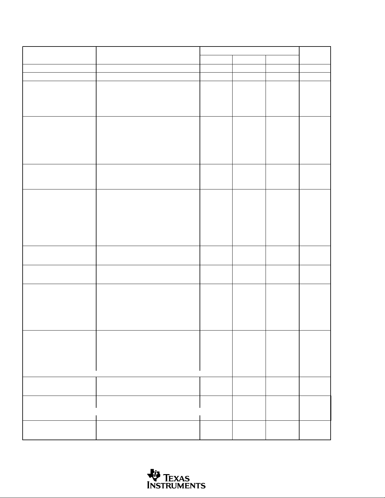
SPECIFICATIONS
At TA = +25°C, VCC = +3.0V, DRVDD = +3.0V, Conversion Rate (f
PARAMETER CONDITIONS MIN TYP MAX UNITS
RESOLUTION 12 Bits
CONVERSION RATE 20 MHz
DIGITAL INPUT
Logic Family TTL
Input Voltage LOW to HIGH Threshold Voltage (VT+) 1.7 V
HIGH to LOW Threshold Voltage (VT–) 1.0 V
Input Current Logic HIGH (I
Logic LOW (I
DIGITAL OUTPUT
Logic Family CMOS
Logic Coding Straight Binary
Output Voltage Logic HIGH (V
Logic LOW (V
ADCCK Clock Duty Cycle 50 %
Input Capacitance 5pF
Maximum Input Voltage –0.3 5.3 V
ANALOG INPUT (CCDIN)
Input Signal Level for Full-Scale Out
PGA Gain = 0dB 900 mV
Input Capitance 15 pF
Input Limit –0.3 3.3 V
TRANSFER CHARACTERISTICS
Differential Non-Linearity (DNL) PGA Gain = 0dB ±0.5 LSB
Integral Non-Linearity (INL) PGA Gain = 0dB ±1 LSB
No Missing Codes Guaranteed
Step Response Settling Time Full-Scale Step Input 1 Pixel
Overload Recovery Time Step Input from 1.8V to 0V 2 Pixels
Data Latency 9 (Fixed) Clock Cycles
Signal-to-Noise Ratio
(1)
Grounded Input Cap, PGA Gain = 0dB 79 dB
Grounded Input Cap, Gain = +24dB 55 dB
CCD Offset Correction Range –180 200 mV
CDS
Reference Sample Settling Time Within 1LSB, Driver Impedance = 50Ω 11 ns
Data Sample Settling Time Within 1LSB, Driver Impedance = 50Ω 11 ns
INPUT CLAMP
Clamp-On Resistance 400 Ω
Clamp Level 1.5 V
PROGRAMMABLE GAIN AMP (PGA)
Gain-Control Resolution 10 Bits
Maximum Gain Gain Code = 1111111111 42 dB
High Gain Gain Code = 1101001000 34 dB
Medium Gain Gain Code = 1000100000 20 dB
Low Gain Gain Code = 0010000000 0 dB
Minimum Gain Gain Code = 0000000000 –6dB
Gain Control Error ±0.5 dB
OPTICAL BLACK CLAMP LOOP
Control DAC Resolution 10 Bits
Optical Black Clamp Level Programmable Range of Clamp Level 2 60 LSB
OBCLP Level at CODE = 1000 130 LSB
Min Output Current for Control DAC
Max Output Current for Control DAC
Loop Time Constant C
Slew Rate C
= 0.1µF, Output Current from Control DAC is Saturated 1530 V/s
COB
COB Pin ±0.15 µA
COB Pin ±153 µA
COB
REFERENCE
Positive Reference Voltage 1.75 V
Negative Reference Voltage 1.25 V
POWER SUPPLY
Supply Voltage V
Power Dissipation Normal Operation Mode: No Load, DAC0 and DAC1 are Suspended 86 mW
CC
Stand-By Mode: f
TEMPERATURE RANGE
Operating Temperature –25 +85 °C
Thermal Resistance
θ
JA
LQFP-48 100 °C/W
NOTE: (1) SNR = 20 log(full-scale voltage/rms noise).
) = 20MHz, unless otherwise noted.
ADCCK
VSP2262Y
) VIN = +3V ±20 µA
IH
) VIN = 0V ±20 µA
IL
) IOH = –2mA 2.4 V
OH
) IOL = 2mA 0.4 V
OL
= 0.1µF µs
, DRV
DD
= Not Apply 6 mW
ADCCK
2.7 3.0 3.6 V
2
VSP2262
SBMS011
Page 3
ABSOLUTE MAXIMUM RATINGS
Supply Voltage: VCC, DRVDD...........................................................+4.0V
Supply-Voltage Differences: Among V
Ground-Voltage Differences: Among GNDA .................................... ±0.1V
Digital Input Voltage ............................................................ –0.3 to +5.3V
Analog Input Voltage .................................................. –0.3 to V
Input Current (Any Pins Except Supplies) ..................................... ±10mA
Ambient Temperature Under Bias .....................................–40 to +125°C
Storage Temperature .........................................................–55 to +125°C
Junction Temperature .................................................................... +150°C
Lead Temperature (Soldering, 5s) ................................................ +260°C
Package Temperature (IR Reflow, Peak, 10s) ............................. +235°C
NOTE: (1) Stresses above these ratings may cause permanent damage.
Exposure to absolute maximum conditions for extended periods may
degrade device reliability.
(1)
......................................... ±0.1V
CC
CC
+ 0.3V
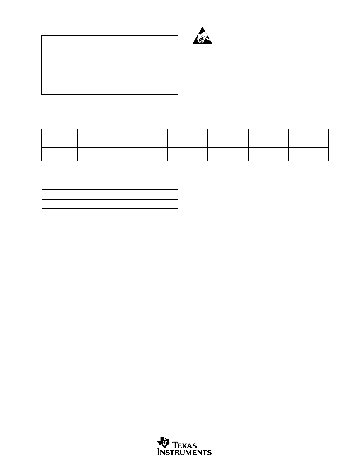
ELECTROSTATIC
DISCHARGE SENSITIVITY
This integrated circuit can be damaged by ESD. Burr-Brown
recommends that all integrated circuits be handled with
appropriate precautions. Failure to observe proper handling
and installation procedures can cause damage.
ESD damage can range from subtle performance degradation to complete device failure. Precision integrated circuits
may be more susceptible to damage because very small
parametric changes could cause the device not to meet its
published specifications.
PACKAGE/ORDERING INFORMATION
PACKAGE SPECIFIED
PRODUCT PACKAGE NUMBER RANGE MARKING NUMBER
DRAWING TEMPERATURE PACKAGE ORDERING TRANSPORT
VSP2262Y LQFP-48 340 0 to +85°C VSP2262Y VSP2262Y 250-Piece Tray
(1)
MEDIA
"""""VSP2262Y/2K Tape and Reel
NOTE: (1) Models with a slash (/) are available only in Tape and Reel in the quantities indicated (e.g., /2K indicates 2000 devices per reel). Ordering 2000 pieces
of “VSP2262Y/2K” will get a single 2000 piece Tape and Reel.
DEMO BOARD ORDERING INFORMATION
PRODUCT ORDERING NUMBER
VSP2262Y DEM-VSP2262Y
VSP2262
SBMS011
3
Page 4
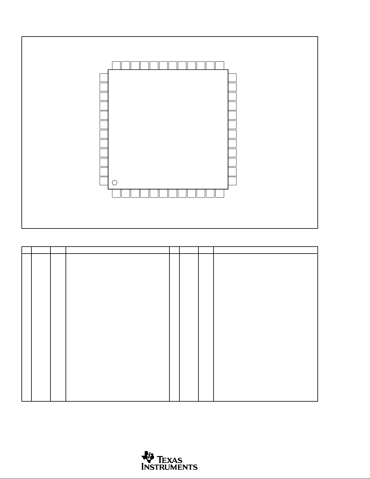
PIN CONFIGURATION
Top View LQFP
GNDA
GNDA
VCCVCCBYPM
36 35 34 33 32 31 30
BYP
CCDIN
BYPP2
COB
VCCGNDA
29 28 27 26
GNDA
CM
REFP
REFN
V
CC
GNDA
GNDA
NC
NC
RESET
SLOAD
SDATA
SCLK
37
38
39
40
41
42
43
VSP2262
44
45
46
47
48
24
23
22
21
20
19
18
17
16
15
14
13
V
CC
CLPDM
SHD
SHP
CLPOB
PBLK
V
CC
GNDA
ADCCK
GNDA
DRVGND
DRV
DD
12345678910112512
B1
B2
B3
B4
B5
B6
B7
B8
B9
B10
B0 (LSB)
B11 (MSB)
PIN DESCRIPTIONS
(1)
PIN NAME TYPE
1 B0 (LSB) DO Bit 0 (LSB), A/D Converter Output
2 B1 DO Bit 1, A/D Converter Output
3 B2 DO Bit 2, A/D Converter Output
4 B3 DO Bit 3, A/D Converter Output
5 B4 DO Bit 4, A/D Converter Output
6 B5 DO Bit 5, A/D Converter Output
7 B6 DO Bit 6, A/D Converter Output
8 B7 DO Bit 7, A/D Converter Output
9 B8 DO Bit 8, A/D Converter Output
10 B9 DO Bit 9, A/D Converter Output
11 B10 DO Bit 10, A/D Converter Output
12
B11 (MSB)
13 DRV
14 DRVGND P Digital Ground, Exclusively for Digital Output
DD
15 GNDA P Analog Ground
16 ADCCK DI Clock for Digital Output Buffer
17 GNDA P Analog Ground
18 V
CC
19 PBLK DI Preblanking:
20 CLPOB DI Optical Black Clamp Pulse (Default = Active LOW)
21 SHP DI
22 SHD DI CDS Data Level Sampling Pulse (Default = Active LOW)
23 CLPDM DI Dummy Pixel Clamp Pulse (Default = Active LOW)
DESCRIPTION
DO Bit 11 (MSB), A/D Converter Output
P Power Supply, Exclusively for Digital Output
P Analog Power Supply
HIGH = Normal Operation Mode
LOW = Preblanking Mode: Digital Output “All Zero”
CDS Reference Level Sampling Pulse (Default = Active LOW)
PIN NAME
24 V
CC
25 GNDA P Analog Ground
26 GNDA P Analog Ground
27 V
CC
28 COB AO Optical Black Clamp Loop Reference
29 BYPP2 AO Internal Reference P
30 CCDIN AI CCD Signal Input
31 BYP AO Internal Reference C
32 BYPM AO Internal Reference N
33 V
CC
34 V
CC
35 GNDA P Analog Ground
36 GNDA P Analog Ground
37 CM AO A/D Converter Common-Mode Voltage
38 REFP AO A/D Converter Positive Reference
39 REFN AO A/D Converter Negative Reference
40 V
CC
41 GNDA P Analog Ground
42 GNDA P Analog Ground
43
NC
44
(5)
(5)
(5)
(5)
NC
45 RESET DI Asynchronous System Reset (Active LOW)
46 SLOAD DI Serial Data Latch Signal (Triggered at the Rising Edge)
47 SDATA DI Serial Data Input
48 SCLK DI Clock for Serial Data Shift (Triggered at the Rising Edge)
NOTES: (1) Type designators: P = Power Supply and Ground; DI = Digital Input; DO = Digital Output; AI = Analog Input; AO = Analog Output. (2) Should be
connected to ground with a bypass capacitor. We recommend the value of 0.1µF to 0.22 µF, however, it depends on the application environment. Refer to the “Optical
Black Level Clamp Loop” section for more detail. (3) Should be connected to ground with a bypass capacitor. We recommend the value of 400pF to 9000pF, however,
it depends on the application environment. Refer to the “Voltage Reference” section for more detail. (4) Should be connected to ground with a bypass capacitor
(0.1µF). Refer to the “Voltage Reference” section for more detail. (5) Refer to “Serial Interface” section for more detail.
(1)
TYPE
DESCRIPTION
P Analog Power Supply
P Analog Power Supply
P Analog Power Supply
P Analog Power Supply
P Analog Power Supply
– Should be Left OPEN
– Should be Left OPEN
(3)
(2)
(4)
(3)
(4)
(4)
(4)
4
VSP2262
SBMS011
Page 5
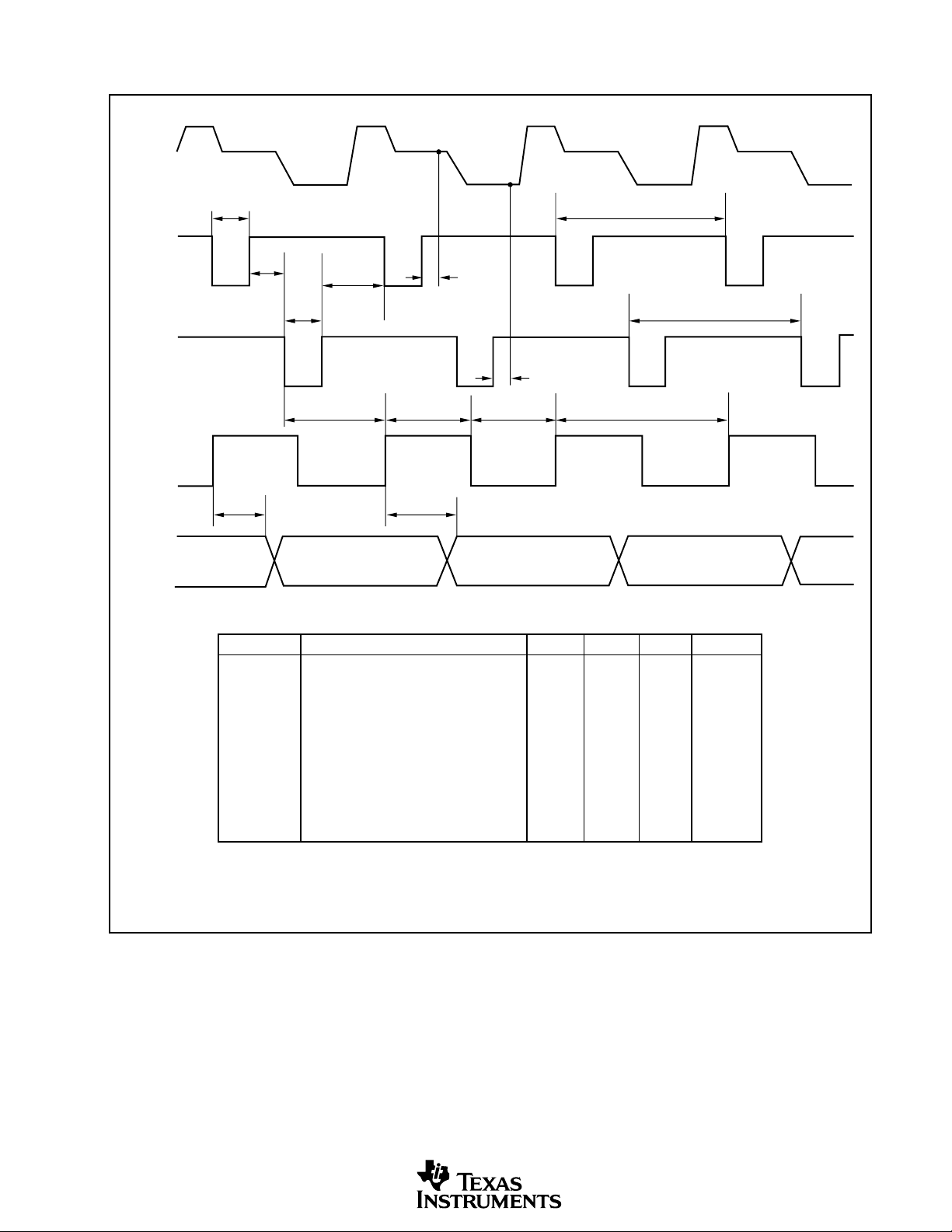
CDS TIMING SPECIFICATIONS
CCD
Output
Signal
N
N + 1 N + 2 N + 3
SHP
SHD
ADCCK
B[11:0]
t
WP
(1)
(1)
t
HOLD
t
PD
t
WD
t
INHIBIT
t
DP
t
t
S
t
S
t
ADC
OD
t
ADC
t
CKP
t
CKP
t
CKP
N – 9N – 8N – 7N – 11 N – 10
SYMBOL PARAMETER MIN TYP MAX UNITS
t
CKP
t
ADC
t
WP
t
WD
t
PD
t
DP
t
t
INHIBIT
t
HOLD
t
OD
ADCCK HIGH/LOW Pulse Width 20 ns
SHP Trailing Edge to SHD Leading Edge
SHD Trailing Edge to SHP Leading Edge
S
Clock Period 48 ns
SHP Pulse Width 14 ns
SHD Pulse Width 11 ns
(1)
8ns
(1)
12 ns
Sampling Delay 5 ns
Inhibited Clock Period 20 ns
Output Hold Time 7 ns
Output Delay 38 ns
DL Data Latency, Normal Operation Mode 9 (fixed) Clock Cycles
NOTE: (1) The description and timing diagrams in this data sheet are all based on the polarity of Active LOW
(default value). The user can select the active polarity (Active LOW or Active HIGH) through the serial interface.
Refer to the “Serial Interface” section for more detail.
VSP2262
SBMS011
5
Page 6

SERIAL INTERFACE TIMING SPECIFICATIONS
t
SLOAD
XS
t
XH
SCLK
SDATA
t
t
CKH
t
t
DS
DH
CKL
t
CKP
MSB
2 Bytes
SYMBOL PARAMETER MIN TYP MAX UNITS
t
t
t
CKP
CKH
CKL
t
DS
t
DH
t
XS
t
XH
Clock Period 100 ns
Clock HIGH Pulse Width 40 ns
Clcok LOW Pulse Width 40 ns
Data Setup Time 30 ns
Data Hold TIme 30 ns
SLOAD to SCLK Setup Time 30 ns
SCLK to SLOAD Hold Time 30 ns
NOTES: (1) Data shift operation should occur at the rising edge of SCLK while SLOAD is LOW. Two bytes of input
data are loaded to the parallel latch in the VSP2260 at the rising edge of SLOAD. (2) When the input serial data
is longer than two bytes (16 bits), the last two bytes become effective and the former bits are lost.
LSB
6
VSP2262
SBMS011
Page 7
THEORY OF OPERATION
INTRODUCTION
The VSP2262 is a complete mixed-signal IC that contains
all of the key features associated with the processing of the
CCD imager output signal in a video camera, a digital still
camera, security camera, or similar applications (see the
simplified block diagram on page 1 for details). The VSP2262
includes a Correlated Double Sampler (CDS), Programmable Gain Amplifier (PGA), Analog-to-Digital Converter
(ADC), input clamp, Optical Black (OB) level clamp loop,
serial interface, timing control, reference voltage generator,
and general-purpose 8-bit Digital-to-Analog Converters
(DAC). We recommend an off-chip emitter follower buffer
between the CCD output and the VSP2262 CCDIN input.
The PGA gain control, clock polarity setting, and operation
mode can be selected through the serial interface. All parameters are reset to the default value when the RESET pin goes
LOW asynchronously from the clocks.
capacitance can be seen at the input pin. The analog input
signal range at the CCDIN pin is 1Vp-p, and the appropriate
common-mode voltage for the CDS is around 0.5V to 1.5V.
The reference level is sampled during SHP active period,
and the voltage level is held on sampling capacitor C
at the
1
trailing edge of SHP. The data level is sampled during SHD
active period, and the voltage level is held on the sampling
capacitor C
at the trailing edge of SHD. The switched-
2
capacitor amplifier then performs the subtraction of these
two levels.
The user can select the active polarity of SHP/SHD (Active
HIGH or Active LOW) through the serial interface (refer to
the “Serial Interface” section for more detail). The default
value of SHP/SHD is “Active LOW”. However, immediately
after power ON, this value is Unknown. For this reason, the
appropriate value must be set by using the serial interface, or
reset to the default value by strobing the RESET pin. The
descriptions and the timing diagrams in this data sheet are all
based on the polarity of Active LOW (default value).
CORRELATED DOUBLE SAMPLER (CDS)
The output signal of a CCD imager is sampled twice during
one pixel period: once at the reference interval and the other
at the data interval. Subtracting these two samples from each
other extracts the video information of the pixel as well as
removes any noise that is common, or correlated, to both the
intervals. Thus, the CDS is very important in reducing the
reset noise and low-frequency noises that are present on the
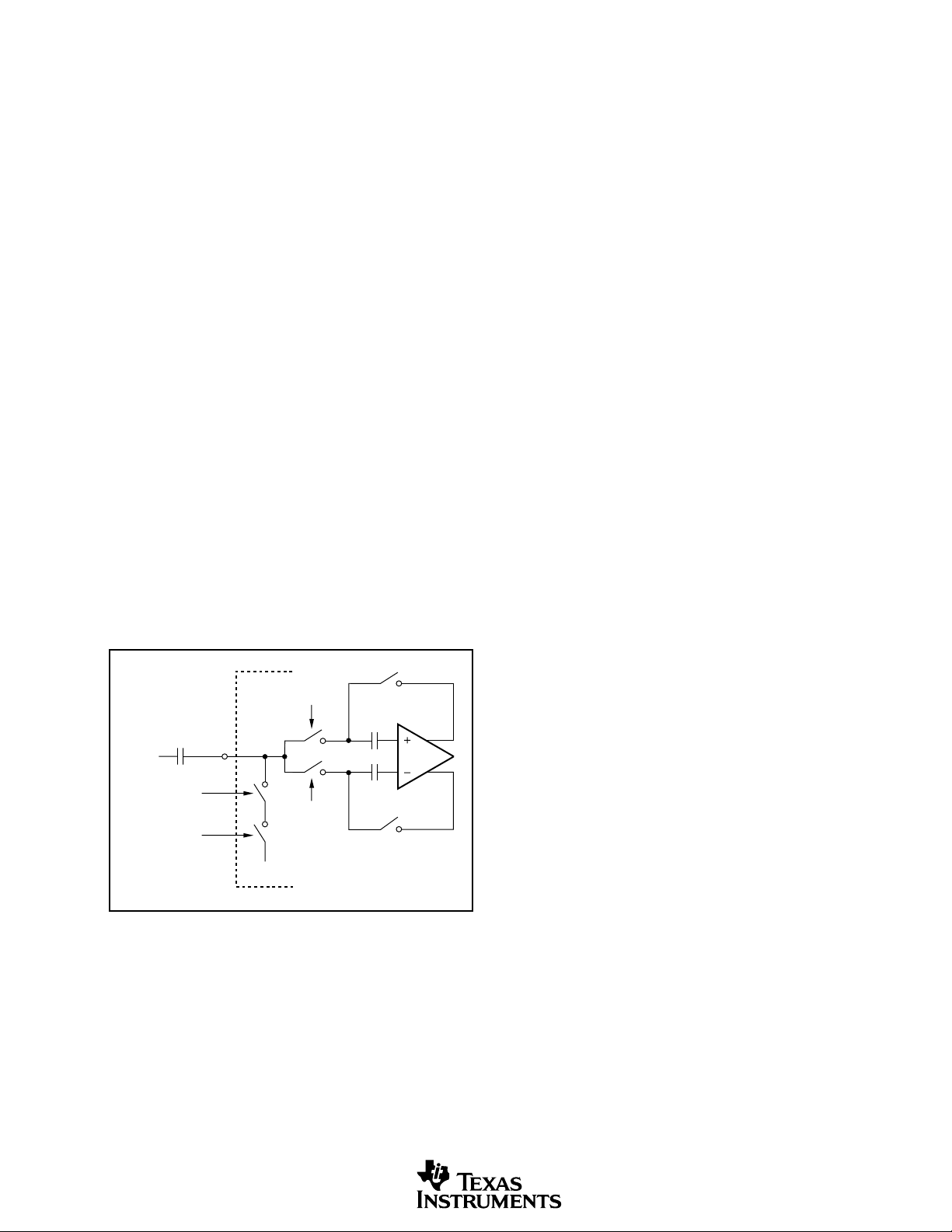
CCD output signal. Figure 1 shows the simplified block
diagram of the CDS and input clamp.
CCD
Output
C
IN
CLPDM
SHP
VSP2262
CCDIN
CM (1.5V)
SHP
SHD
C
10pF
C
10pF
1
OPA
2
FIGURE 1. Simplified Block Diagram of CDS and Input
Clamp.
INPUT CLAMP OR DUMMY PIXEL CLAMP
The buffered CCD output is capacitively coupled to the
VSP2262. The purpose of the input clamp is to restore the
DC component of the input signal that was lost with the AC
coupling and establish the desired DC bias point for the
CDS. A simplified block diagram of the input clamp is
shown in Figure 1. The input level is clamped to the internal
reference voltage, CM (1.5V), during the dummy pixel
interval. More specifically, when both CLPDM and SHP are
active, the dummy clamp function becomes active. If the
dummy pixels and/or the CLPDM pulse are not available in
your system, the CLPOB pulse can be used in place of
CLPDM, as long as the clamping takes place during black
pixels. In this case, both the CPLDM pin (active at same
timing as CLPOB) and SHP become active during the
optical black pixel interval, and then the dummy clamp
function becomes active.
The active polarity of CLPDM and SHP (Active HIGH or
Active LOW) can be selected through the serial interface
(refer to the “Serial Interface” section for more detail).
The default value of CLPDM and SHP is “Active LOW”.
However, immediately after power ON, this value is Unknown. For this reason, the appropriate value must be set by
using the serial interface, or reset to the default value by
strobing the RESET pin. The descriptions and the timing
diagrams in this data sheet are all based on the polarity of
Active LOW (default value).
The CDS is driven through an off-chip coupling capacitor
(C
). AC coupling is strongly recommended because the
IN
DC level of the CCD output signal is usually several volts
too high for the CDS to work properly.
A 0.1µF capacitor is recommended for C
, depending on
IN
the application environment. Additionally, we recommend
an off-chip emitter follower buffer that can drive more than
10pF, because the 10pF capacitor and a few pF of stray
VSP2262
SBMS011
HIGH PERFORMANCE ANALOG-TO-DIGITAL
CONVERTER (ADC)
The ADC utilizes a fully differential and pipelined architecture. This ADC is well suited for low-voltage operations,
low power consumption requirements, and high-speed applications. It guarantees 12-bit resolution with no missing
codes. The VSP2262 includes a reference voltage generator
for the ADC. REFP (Positive Reference, pin 38), REFN
7
Page 8

(Negative Reference, pin 39), and CM (Common-Mode
Voltage, pin 37) should be bypassed to ground with a 0.1µF
ceramic capacitor and should not be used elsewhere in the
system, as they affect the stability of these reference levels,
which causes ADC performance degradation. Note that
these are analog output pins and, therefore, do not apply
external voltage.
PROGRAMMABLE GAIN AMPLIFIER (PGA)
Figure 2 shows the characteristics of the PGA gain. The PGA
provides a gain range of –6dB to +42dB, which is linear in dB.
The gain is controlled by a digital code with
10-bit resolution, and can be set through the serial interface
(refer to the “Serial Interface” section for more detail). The
default value of the gain control code is 128 (PGA Gain =
0dB)
.
However, immediately after power ON, this value is
Unknown. For this reason, the appropriate value must be set
by using the serial interface, or reset to the default value by
strobing the RESET pin.
50
40
30
20
Gain (dB)
10
0
–10
0
100
200
300
400
Input Code for Gain Control (0 to 1023)
500
600
700
800
900
1k
1023
FIGURE 2. The Characteristics of PGA Gain.
OPTICAL BLACK (OB) LEVEL CLAMP LOOP
To extract the video information correctly, the CCD signal
must be referenced to a well-established OB level. The
VSP2262 has an auto-calibration loop to establish the OB
level using the optical black pixels output from the CCD
imager. The input signal level of the OB pixels is identified
as the real “OB level”, and the loop should be closed while
CLPOB is active.
During the effective pixel interval, the reference level of the
CCD output signal is clamped to the OB level by the OB
level clamp loop. To determine the loop time constant, an
off-chip capacitor is required, and should be connected to
COB (pin 28). Time constant T is given in the following
equation:
T = C/(16384 • I
Where C is the capacitor value connected to COB, I
MIN
)
is the
MIN
minimum current (0.15µA) of the control Digital-to-Analog
Converter (DAC) in the OB level clamp loop, and 0.15µA is
equivalent to 1LSB of the DAC output current. When C is
0.1µF, time constant T is 40.7µs.
Additionally, the slew rate SR is given the following equa-
tion:
MAX
/C
MAX
is
SR = I
Where C is the capacitor value connected to COB, I
the maximum current (153µA) of the control DAC in the OB
level clamp loop, and 153µA is equivalent to 1023LSB of
the DAC output current.
Generally, OB level clamping at high speed causes “Clamp
Noise” (or “White Streak Noise”), however, the noise will
decrease by increasing C. On the other hand, an increased C
requires a much longer time to restore from Stand-by mode,
or right after power ON. Therefore, we consider 0.1µF to
0.22µF a reasonable value for C. However, it depends on the
application environment; we recommend making careful
adjustments using trial-and-error.
The “OB clamp level” (the pedestal level) is programmable
through the serial interface (refer to the “Serial Interface”
section for more detail). Table I shows the relationship
between input code and the OB clamp level.
INPUT CODE OB CLAMP LEVEL, LSBs OF 12 BITS
0000 2LSB
0001 18LSB
0010 34LSB
0011 50LSB
0100 66LSB
0101 82LSB
0110 98LSB
0111 114LSB
1000 (Default) 130LSB
1001 146LSB
1010 162LSB
1011 178LSB
1100 194LSB
1101 210LSB
1110 226LSB
1111 242LSB
TABLE I. Programmable OB Clamp Level.
The active polarity of CLPOB (Active HIGH or Active
LOW) can be selected through the serial interface (refer to
the “Serial Interface” section for more detail). The default
value of CLPOB is “Active LOW”. However, immediately
after power ON, this value is Unknown. For this reason, the
appropriate value must be set by using the serial interface, or
reset to the default value by strobing the RESET pin. The
descriptions and the timing diagrams in this data sheet are all
based on the polarity of Active LOW (default value).
PREBLANKING AND DATA LATENCY
The VSP2262 has an input blanking, or preblanking, function. When PBLK goes LOW, all digital outputs will go to
ZERO at the 11th rising edge of ADCCK. In this mode, the
digital output data comes out on the rising edge of ADCCK
with a delay of 11 clock cycles (data latency is 11). This is
8
VSP2262
SBMS011
Page 9

different from the preblanking mode in which the digital
output data comes out on the rising edge of ADCCK with a
delay of nine clock cycles (data latency is nine).
If the input voltage is higher than the supply rail by 0.3V or
lower than the ground rail by 0.3V, the protection diodes
will be turned on to prevent the input voltage from going any
further. Such a high swing signal may cause device damage
to the VSP2262 and should be avoided.
STAND-BY MODE
For the purpose of saving power, the VSP2262 can be set to
Stand-by mode (or Power-Down mode) through the serial
interface when the VSP2262 is not in use. Refer to the
“Serial Interface” section for more detail. In this mode, all
the function blocks are disabled and the digital outputs will
go to all ZEROs, causing the current consumption to drop to
1mA. Since all the bypass capacitors will discharge during
this mode, a substantial time (usually of the order of 200ms
to 300ms) is required to power up from Stand-by mode.
VOLTAGE REFERENCE
All the reference voltages and bias currents needed in the
VSP2262 are generated by its internal bandgap circuitry.
The CDS and the ADC use mainly three reference voltages:
REFP (Positive Reference, pin 38), REFN (Negative Reference, pin 39) and CM (Common-Mode Voltage, pin 37).
REFP, REFN and CM should be heavily decoupled with
appropriate capacitors (e.g., 0.1µF ceramic capacitor). Do
not use these voltages elsewhere in the system as they affect
the stability of the reference level, and cause ADC performance degradation. Note that these are analog output pins
and do not apply external voltage.
BYPP2 (pin 29), BYP (pin 31), and BYPM (pin 32) are also
reference voltages to be used in the analog circuit. BYP
should be connected to ground with a 0.1µF ceramic capacitor. Since the capacitor value for BYPP2 and BYPM affects
the step response, we consider 400pF to 9000pF to be a
reasonable value. However, as it depends on the application
environment, we recommend making careful adjustments
using trial-and-error.
BYPP2, BYP and BYPM should all be heavily decoupled
with appropriate capacitors, and not used elsewhere in the
system. They affect the stability of the reference levels, and
cause performance degradation. Note that these are analog
output pins and do not apply external voltage.
SERIAL INTERFACE
The serial interface has a 2-byte shift register and various
parallel registers to control all the digitally programmable
features of the VSP2262. Writing to these registers is controlled by four signals (SLOAD, SCLK, SDATA, and RESET). To enable the shift register, SLOAD must be pulled
LOW. SDATA is the serial data input and the SCLK is the
shift clock. The data at SDATA is taken into the shift
register at the rising edge of SCLK; the data length should
be two bytes. After the 2-byte shift operation, the data in the
shift register is transferred to the parallel latch at the rising
edge of SLOAD. In addition to the parallel latch, there are
several registers dedicated to the specific features of the
device and are synchronized with ADCCK. It takes five or
six clock cycles for the data in the parallel latch to be written
to those registers. Therefore, to complete the data updates, it
requires five or six clock cycles after parallel latching by the
rising edge of SLOAD.
See Table II for the serial interface data format. TEST is the
flag for the test mode (Texas Instruments proprietary only),
A0 to A2 is the address for the various registers, and D0 to
D11 is the data (or operand) field.
VSP2262
SBMS011
9
Page 10

MSB LSB
REGISTERS TEST A2 A1 A0 D11 D10 D9 D8 D7 D6 D5 D4 D3 D2 D1 D0
Configuration 000000000000 00 0C0
PGA Gain 000100G9G8G7G6G5G4G3G2G1G0
OB Clamp Level 001000000000O3O2O1O0
Clock Polarity 001100000000 0P2P1P0
Reserved 0100xxxxxxxx xx x x
Reserved 0101xxxxxxxx xx x x
Reserved 0110xxxxxxxx xx x x
Reserved 0111xxxxxxxx xx x x
Reserved 1 xxxxxxxxxxxxx x x
x = Don’t Care.
TABLE II. Serial Interface Data Format.
REGISTER DEFINITIONS
C[0] Operation Mode, Normal/Stand-By
Serial Interface and Registers are always active, independently from the operation mode.
C0 = Operation Mode for the entire chip except the serial interface and registers.
(C0 = 0 “Active”; C0 = 1 “Stand-by”)
G[9:0] The Characteristics of PGA Gain (refer to Figure 2)
O[3:0] Programmable OB Clamp Level (refer to Table I)
P[2:0] Clock Polarity
P0 = Polarity for CLPDM (P0 = 0 “Active LOW”; P0 = 1 “Active HIGH”)
P1 = for CLPOB (P0 = 0 “Active LOW”; P0 = 1 “Active HIGH”)
P2 = for SHP/SHD (P0 = 0 “Active LOW”; P0 = 1 “Active HIGH”)
Immediately after power ON, these values are Unknown. The appropriate value must be set by using the serial interface, or reset
to the default value by strobing the RESET pin.
Default values are:
C[2:0] = 0 Normal Operation Mode
G[9:0] = 0010000000 PGA Gain = 0dB
O[3:0] = 1000 OB Clamp Level = 32LSB
P[2:0] = 000 CLPDM, CLPOB, SHP/SHD are all “Active LOW”
NOTE: (1) The descriptions and the timing diagrams in this data sheet are all based on the polarity of Active LOW (default value).
(1)
10
VSP2262
SBMS011
Page 11

TIMINGS
The CDS and the ADC are operated by SHP/SHD and their
derivative timing clocks generated by the on-chip timing
generator. The digital output data is synchronized with
ADCCK. See the VSP2262 “CDS Timing Specifications” for
the timing relationship among the CCD signal, SHP/SHD,
ADCCK and the output data. CLPOB is used to activate the
black level clamp loop during the OB pixel interval, and
CLPDM is used to activate the input clamping during the
dummy pixel interval. If the CLPDM pulse is not available in
your system, the CLPOB pulse can be used in place of
CLPDM as long as the clamping takes place during black
pixels (refer to the “Input Clamp and Dummy Pixel Clamp”
section for more detail). The clock polarities of SHP/SHD,
CLPOB and CLPDM can be independently set through the
serial interface (refer to the “Serial Interface” section for more
detail). The descriptions and the timing diagrams in this data
sheet are all based on the polarity of Active LOW (default
value). In order to keep a stable and accurate OB clamp level,
we recommend CLPOB should not be activated during PBLK
active period. Refer to the “Preblanking and Data Latency”
section for more detail. In Stand-by mode, ADCCK, SHP,
SHD, CLPOB and CLPDM are internally masked and pulled
HIGH.
POWER SUPPLY, GROUNDING AND DEVICE
DECOUPLING RECOMMENDATIONS
The VSP2262 incorporates analog circuitry and a very
high-precision, high-speed ADC that are vulnerable to any
extraneous noise from the rails or elsewhere. For this reason,
it should be treated as an analog component and all supply
pins except for DRV
should be powered by the only
DD
analog supply of the system. This will ensure the most
consistent results, since digital power lines often carry high
levels of wideband noise that would otherwise be coupled
into the device and degrade the achievable performance.
Proper grounding, short lead length, and the use of ground
planes are also very important for high-frequency designs.
Multi-layer PC boards are recommended for the best performance, since they offer distinct advantages like minimizing
ground impedance, separation of signal layers by ground
layers, etc. It is highly recommended that analog and digital
ground pins of the VSP2262 be joined together at the IC and
be connected only to the analog ground of the system. The
driver stage of the digital outputs (B[11:0]) is supplied
through a dedicated supply pin (DRV
) and it should be
DD
separated from the other supply pins completely, or at least
with a ferrite bead.
It is also recommended to keep the capacitive loading on the
output data lines as low as possible (typically less than
15pF). Larger capacitive loads demand higher charging
current surges that can feed back into the analog portion of
the VSP2262 and affect the performance. If possible, external buffers or latches should be used, providing the added
benefit of isolating the VSP2262 from any digital noise
activities on the data lines. In addition, resistors in series
with each data line may help minimize the surge current.
Values in the range of 100Ω to 200Ω will limit the instantaneous current the output stage has to provide for recharging the parasitic capacitances as the output levels change
from LOW to HIGH, or HIGH to LOW. Due to high
operation speed, the converter also generates high-frequency
current transients and noises that are fed back into the supply
and reference lines. This requires the supply and reference
pins to be sufficiently bypassed. In most cases, 0.1µF ceramic chip capacitors are adequate to decouple the reference
pins. Supply pins should be decoupled to the ground plane
with a parallel combination of tantalum (1µF to 22µF) and
ceramic (0.1µF) capacitors. The effectiveness of the decoupling largely depends on the proximity to the individual pin.
DRV
should be decoupled to the proximity of DRVGND.
DD
Special attention must be paid to the bypassing of COB,
BYPP2 and BYPM, since these capacitor values determine
important analog performances of the device.
VSP2262
SBMS011
11
Page 12

PACKAGE OPTION ADDENDUM
www.ti.com
30-Mar-2005
PACKAGING INFORMATION
Orderable Device Status
(1)
Package
Type
Package
Drawing
Pins Package
Qty
Eco Plan
VSP2262Y ACTIVE LQFP PT 48 250 TBD CU SNPB Level-1-235C-UNLIM
VSP2262Y/2K ACTIVE LQFP PT 48 2000 TBD CU SNPB Level-1-235C-UNLIM
(1)
The marketing status values are defined as follows:
ACTIVE: Product device recommended for new designs.
LIFEBUY: TI has announced that the device will be discontinued, and a lifetime-buy period is in effect.
NRND: Not recommended for new designs. Device is in production to support existing customers, but TI does not recommend using this part in
a new design.
PREVIEW: Device has been announced but is not in production. Samples may or may not be available.
OBSOLETE: TI has discontinued the production of the device.
(2)
Eco Plan - The planned eco-friendly classification: Pb-Free (RoHS) or Green (RoHS & no Sb/Br) - please check
http://www.ti.com/productcontent for the latest availability information and additional product content details.
TBD: The Pb-Free/Green conversion plan has not been defined.
Pb-Free (RoHS): TI's terms "Lead-Free" or "Pb-Free" mean semiconductor products that are compatible with the current RoHS requirements
for all 6 substances, including the requirement that lead not exceed 0.1% by weight in homogeneous materials. Where designed to be soldered
at high temperatures, TI Pb-Free products are suitable for use in specified lead-free processes.
Green (RoHS & no Sb/Br): TI defines "Green" to mean Pb-Free (RoHS compatible), and free of Bromine (Br) and Antimony (Sb) based flame
retardants (Br or Sb do not exceed 0.1% by weight in homogeneous material)
(3)
MSL, Peak Temp. -- The Moisture Sensitivity Level rating according to the JEDEC industry standard classifications, and peak solder
temperature.
(2)
Lead/Ball Finish MSL Peak Temp
(3)
Important Information and Disclaimer:The information provided on this page represents TI's knowledge and belief as of the date that it is
provided. TI bases its knowledge and belief on information provided by third parties, and makes no representation or warranty as to the
accuracy of such information. Efforts are underway to better integrate information from third parties. TI has taken and continues to take
reasonable steps to provide representative and accurate information but may not have conducted destructive testing or chemical analysis on
incoming materials and chemicals. TI and TI suppliers consider certain information to be proprietary, and thus CAS numbers and other limited
information may not be available for release.
In no event shall TI's liability arising out of such information exceed the total purchase price of the TI part(s) at issue in this document sold by TI
to Customer on an annual basis.
Addendum-Page 1
Page 13

IMPORTANT NOTICE
Texas Instruments Incorporated and its subsidiaries (TI) reserve the right to make corrections, modifications,
enhancements, improvements, and other changes to its products and services at any time and to discontinue
any product or service without notice. Customers should obtain the latest relevant information before placing
orders and should verify that such information is current and complete. All products are sold subject to TI’s terms
and conditions of sale supplied at the time of order acknowledgment.
TI warrants performance of its hardware products to the specifications applicable at the time of sale in
accordance with TI’s standard warranty. T esting and other quality control techniques are used to the extent TI
deems necessary to support this warranty . Except where mandated by government requirements, testing of all
parameters of each product is not necessarily performed.
TI assumes no liability for applications assistance or customer product design. Customers are responsible for
their products and applications using TI components. To minimize the risks associated with customer products
and applications, customers should provide adequate design and operating safeguards.
TI does not warrant or represent that any license, either express or implied, is granted under any TI patent right,
copyright, mask work right, or other TI intellectual property right relating to any combination, machine, or process
in which TI products or services are used. Information published by TI regarding third-party products or services
does not constitute a license from TI to use such products or services or a warranty or endorsement thereof.
Use of such information may require a license from a third party under the patents or other intellectual property
of the third party, or a license from TI under the patents or other intellectual property of TI.
Reproduction of information in TI data books or data sheets is permissible only if reproduction is without
alteration and is accompanied by all associated warranties, conditions, limitations, and notices. Reproduction
of this information with alteration is an unfair and deceptive business practice. TI is not responsible or liable for
such altered documentation.
Resale of TI products or services with statements different from or beyond the parameters stated by TI for that
product or service voids all express and any implied warranties for the associated TI product or service and
is an unfair and deceptive business practice. TI is not responsible or liable for any such statements.
Following are URLs where you can obtain information on other Texas Instruments products and application
solutions:
Products Applications
Amplifiers amplifier.ti.com Audio www.ti.com/audio
Data Converters dataconverter.ti.com Automotive www.ti.com/automotive
DSP dsp.ti.com Broadband www.ti.com/broadband
Interface interface.ti.com Digital Control www.ti.com/digitalcontrol
Logic logic.ti.com Military www.ti.com/military
Power Mgmt power.ti.com Optical Networking www.ti.com/opticalnetwork
Microcontrollers microcontroller.ti.com Security www.ti.com/security
Telephony www.ti.com/telephony
Video & Imaging www.ti.com/video
Wireless www.ti.com/wireless
Mailing Address: Texas Instruments
Post Office Box 655303 Dallas, Texas 75265
Copyright 2005, Texas Instruments Incorporated
 Loading...