

Page 1

Using the UCC28810EVM-002
User's Guide
Literature Number: SLUU355A
March 2009 – Revised June 2009
Page 2

SLUU355A – March 2009 – Revised June 2009
A 0.9-A Constant Current Supply with PFC for 100-W LED
Lighting Applications
1 Introduction
The UCC28810EVM-002 is a constant current non-isolated power supply for LED lighting applications. It
will convert universal mains (90 VRMS to 264 VRMS) to a 0.9-A constant current into a 100-W load. This
evaluation module will allow the customer evaluate the UCC28810/11 in a typical LED lighting application.
2 Description
The evaluation module uses a two stage approach to controlling the output current.
The first stage is a transition mode PFC circuit. This ensures the design meets the harmonic current or
power factor requirements set out by various standards, such as EN61000-3-2. The PFC circuit converts
the AC input to a regulated DC voltage. This DC voltage can be configured in one of two ways. The
default configuration of the module is that of a boost follower type PFC. The boost follower PFC is where
the PFC regulated output DC voltage tracks the AC input peak voltage. The second configuration requires
removing some components and changing a resistor value see below for more details. This second
configuration removes the tracking element of the PFC circuit. The PFC DC output voltage will then be
regulated to a fixed value in the region of 396 VDC.
The second stage also uses transition mode but is configured as a buck converter. It converts the PFC
output voltage to a fixed constant current. This circuit is capable of supplying 0.9 A into a 100-W load. It
also accepts PWM dimming inputs. Alternatively the user can use the PWM circuit on the module to see
the dimming function.
This module will work with most high brightness LED’s (HB-LED) that operate with 0.9 A and a total string
voltage drop of between 55 V and 110 V.
User's Guide
2.1 Typical Applications
• AC Input General Lighting Applications Using HB-LED’s
• Industrial, Commercial and Residential Lighting Fixtures
• Outdoor Lighting: Street, Roadway, Parking, Construction and Ornamental LED Lighting Fixtures
2.2 Features
• 90 VRMS to 264 VRMS operation
• Boost Follower or Fixed Output PFC Stage
• PFC Disable
• Output Current Disable
• External or Internal PWM Dimming
A 0.9-A Constant Current Supply with PFC for 100-W LED Lighting Applications2 SLUU355A – March 2009 – Revised June 2009
Submit Documentation Feedback
Page 3
www.ti.com
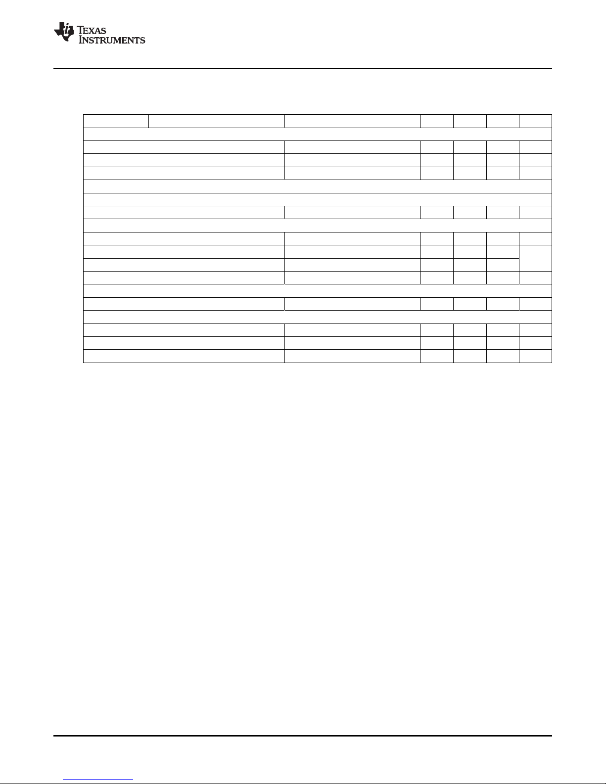
3 Electrical Performance Specifications
SYMBOL PARAMETER CONDITIONS MIN NOM MAX UNITS
INPUT CHARACTERSTICS
V
I
IN
PF Power factor P
OUTPUT CHARACTERSTICS
PFC Stage
V
LED Driver Stage
P
I
OUT
SYSTEMS CHARACTERSTICS
η Full load efficiency 90% 93%
PWM Dimming
Input voltage 90 264 V
IN
Input current 0.175 1.1 A
PFC output voltage 235 415 VDC
OUT
Output power 45 80 100 W
OUT
Output current 0.84 0.9 0.96
Line regulation 0.03
Frequency 60 128 kHz
Threshold 0.72 1.3 V
Frequency range 200 1000 Hz
Duty cycle 0% 90%
Table 1. UCC28810EVM-002 Electrical Performance Specifications
(1)
Electrical Performance Specifications
= 80 W to 100 W 0.95 0.97
OUT
RMS
RMS
A
(1)
The PWM dimming signal is inverted, 0% duty cycle is 100% LED current.
SLUU355A – March 2009 – Revised June 2009 A 0.9-A Constant Current Supply with PFC for 100-W LED Lighting Applications 3
Submit Documentation Feedback
Page 4
++
+
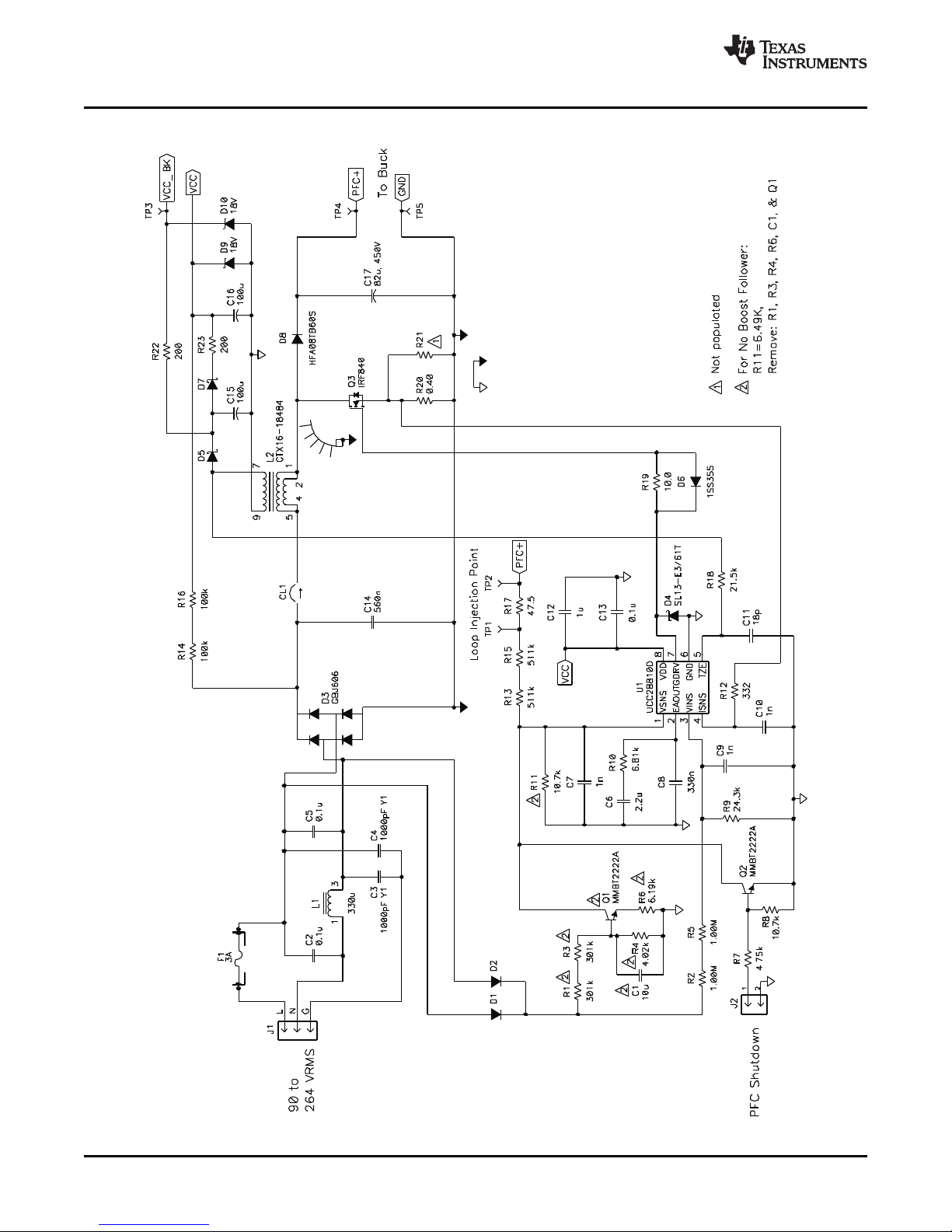
Schematic
www.ti.com
4 Schematic
Figure 1. UCC28810EVM-002 PFC Stage Schematic
4 A 0.9-A Constant Current Supply with PFC for 100-W LED Lighting Applications SLUU355A – March 2009 – Revised June 2009
Submit Documentation Feedback
Page 5

VSENSE
EAOUT
VINS
ISENSE TZE
GND
GDRV
VDD
www.ti.com
Schematic
Figure 2. UCC28810EVM-002 Buck Stage Schematic
SLUU355A – March 2009 – Revised June 2009 A 0.9-A Constant Current Supply with PFC for 100-W LED Lighting Applications 5
Submit Documentation Feedback
Page 6

Test Setup
5 Test Setup
5.1 Test Equipment
See Figure 3 for recommended test set up.
5.1.1 Voltage Source:
• Source 1: Isolated AC voltage source or VARIAC, capable of 90 VRMS to 264 VRMS at 150 W.
• Source 2: A 3.3-V DC source capable of 100 mA.
5.1.2 Multimeters
Three digital multimeters are recommend, one for current measurement, A1, and two for voltage
measurements, V1 and V2.
www.ti.com
WARNING
High voltages, that may cause injury, exist on this evaluation
module (EVM). Please ensure all safety procedures are followed
when working on this EVM. Never leave a powered EVM
unattended. The use of isolated test equipment is highly
recommended.
5.1.3 Output Load
It is recommended that actual high brightness LED’s (HB-LED’s) are used for the load. They should be
rated at 0.9 A. The HB-LED’s should be connected in series. Their voltage drop should be between 55
VDC and 110 VDC. Alternatively a constant voltage electronic load could be used. If using a constant
voltage electronic load a 1000- µ F/250 VDC capacitor is required at the input to the electronic load. The
1000 µ F capacitor should not be used if using HB-LED’s as the load.
5.1.4 Oscilloscope
A digital or analog oscilloscope with current probe is required to view the AC current in the PFC inductor
or buck inductor.
5.1.5 Signal Generator
A signal generator that can produce a square wave pulse train at between 200 Hz and 1 kHz is required
to do external PWM dimming.
5.1.6 Fan
Forced air cooling is not required
5.1.7 Recommended Wire Gauge
A minimum of 18 AWG wire is recommended. Also the wire connections between the AC source and the
EVM, and the EVM and load should be less than two feet long. The AC input connector accepts a
standard IEC320-C13 connector with ground pin.
A 0.9-A Constant Current Supply with PFC for 100-W LED Lighting Applications6 SLUU355A – March 2009 – Revised June 2009
Submit Documentation Feedback
Page 7

TP3
Buckbiasvoltagemonitor
TP4&TP5
PFCoutputvoltage
TP1&TP2
Loopinjectionpoint
CL2
CurrentProbe:
Buckinductor
ripplecurrent
monitor
J3
ShortpinstoEnable
OnBoardDimming
+
L N
V2
CL1
CurrentProbe:
PFCinductor
ripplecurrent
monitor
1000uF
250V
A1
V1
J4
Pin1:BuckShutdown
Pin2:GND
Pin3ExternalPWMdimminginput
J2
Pin1:PFCShutdown
Pin2:GND
IEC320
-C13
Plug
90-265
VRMS
ACSource
Constant
Voltage
Load
+ -
www.ti.com
5.2 Recommended Test Setup
Test Setup
Figure 3. UCC28810EVM-002 Recommended Test Set Up
Note: The 1000- µ F/250-V capacitor on the output is not required if the load is a string of HB-LED’s.
5.3 List of Test Points
Table 2. Test Point Functions
TEST POINTS NAME DESCRIPTION
TP1 Loop injection point
TP2 Loop injection point, PFC output
TP3 VCC_BK Buck bias voltage output
TP4 PFC+ PFC output voltage
TP5 PFC- PFC output voltage ground
TP6 VCC_BK Buck bias voltage input
TP7 GND Buck bias voltage ground
TP8 GND Ground connection
TP9 EN Buck enable
TP10 GND Buck input voltage ground
TP11 BK_IN Buck input voltage
J2-1 PFC shutdown Apply 3.3 V to this pin to shutdown PFC stage
J2-2 GND
J4-1 BK_Shutdown Apply 3.3 V to this pin to shutdown buck stage
J4-2 GND
J4-3 PWM Dim Input for external PWM dimming
J3 On board dim
Short the two pins on J3 to enable on board PWM diming. R26
varies dimming duty cycle
SLUU355A – March 2009 – Revised June 2009 A 0.9-A Constant Current Supply with PFC for 100-W LED Lighting Applications 7
Submit Documentation Feedback
Page 8

Test Procedure
6 Test Procedure
All tests will use the set up described in Section 5 of this user guide. Ensure potentiometer R26 is rotated
completely clockwise.
HIGH VOLTAGE levels are present on this evaluation module
whenever it is energized. Proper precautions must be observed
whenever working with this module. There is an energy storage
capacitor (C17) on this module which must be discharged before
the board can be handled. Serious injury can occur if proper safety
procedures are not followed.
6.1 Applying Power to the EVM
1. Set up the EVM as described in Section 5 of this user guide.
2. Ensure the AC source is off.
3. Ensure potentiometer R26 is rotated completely clockwise.
4. Set constant voltage load to between 55 V and 110 V. If using a HB-LED string ensure the voltage
drop, when operating, is between 55 V to 110 V nominal. Note the 1000- µ F/250 V capacitor is not
required on the output if using a HB-LED string.
5. Set AC source to 90 VRMS.
6. Turn on AC source.
7. Monitor PFC output voltage at TP4 and TP5, V2.
8. Monitor output current at A1.
9. Monitor output voltage at V1.
10. The EVM is now ready for testing.
www.ti.com
WARNING
6.2 Line/Load Regulation and Efficiency Measurement Procedure
1. Apply power to the EVM per Section 6.1 .
2. Vary the constant voltage load from 110 V to 55 V.
3. Observe output current on A1 stays constant.
4. Vary AC source from 90 VRMS to 264 VRMS.
5. Observe output current on A1 stays constant.
6. PFC inductor ripple current can be measured at CL1 using an oscilloscope and current probe.
7. The buck output inductor current can be measured at CL2 using an oscilloscope and current probe.
8. See Section 7 for some typical test results.
6.3 PFC Disable
1. Ensure the AC source is off.
2. Connect a DC source to J2.
3. Set DC source to 0 V.
4. Apply power to the EVM per Section 6.1 .
5. Increase DC source to 3.3 V. This input can accept up to 12 V.
6. Observe PFC output voltage reduces, V2.
7. PFC inductor ripple current looses high frequency component.
A 0.9-A Constant Current Supply with PFC for 100-W LED Lighting Applications8 SLUU355A – March 2009 – Revised June 2009
Submit Documentation Feedback
Page 9

www.ti.com
6.4 Buck Disable
1. Ensure the AC source is off.
2. Connect a DC source to J4, pins 1 and 2.
3. Set DC source to 0 V.
4. Apply power to the EVM per Section 6.1 .
5. Increase DC source to 3.3 V. This input can accept up to 12 V.
6. Observe output current, A1, drops to zero.
7. PFC voltage, V2, does not change.
6.5 Internal Dimming Function
1. Ensure the AC source is off.
2. Ensure jumper is present on J3.
3. Apply power to the EVM per Section 6.1 .
4. Rotate R26 potentiometer slowly anti clockwise.
5. Observe output current on A1 reduce from nominal 0.9 A to 0.1 A. If LED string is attached observe
LED’s dim.
6.6 External Dimming Function
1. Ensure the AC source is off.
2. Ensure jumper is removed from J3.
3. Connect signal generator to J4, pins 3 and 2.
4. Set signal generator to generator a pulse from 0 V to 3.3 V at 200 Hz with variable duty cycle. Note
when the PWM signal is high the LED light is reduced. 100% duty cycle will turn LED off.
5. Apply power to the EVM per Section 6.1 .
6. Vary the duty cycle of the signal generator output.
7. Observe output current, A1, changes. If an LED string is attached observe LED’s dim.
Test Procedure
6.7 Configuring the PFC Stage for Fixed Output
The EVM ships configured as a boost follower PFC. Using a soldering iron some simple component
modifications can change the PFC configuration from boost follower to fixed output voltage.
1. Remove R1, R3, R4, R6, C1 and Q1.
2. Change R11 to 6.49 k Ω .
3. The EVM now uses a fixed output voltage PFC stage. Repeat tests to see functionality.
6.8 Equipment Shutdown
1. If DC sources are connected to shutdown pins, J2 and J4, ensure they are set to 0 V.
2. Ensure load is at maximum, this will help discharge C17.
3. Turn off AC source.
4. Monitor PFC output voltage V2. Do not handle EVM until V2 reads less than 50 VDC.
SLUU355A – March 2009 – Revised June 2009 A 0.9-A Constant Current Supply with PFC for 100-W LED Lighting Applications 9
Submit Documentation Feedback
Page 10

80 100 120 140 200 220 260
V
RMS
-LineVoltage-V
0.88
0.98
1.00
160 180 240
0.92
0.94
PF - Power Factor and Efficiency - %
EFFICIENCY/POWERFACTOR
vs
LINEVOLTAGE
Efficiency
PowerFactor
0.90
0.96
0
2
4
10
12
6
8
THD - Total Harmonic Distortion - %
80 100 120 140 200 220 260
V
RMS
-LineVoltage-V
160 180 240
TOTAL HARMONICDISTORTION
vs
LINEVOLTAGE
Ch2:
BuckV
DS
Ch4:
LEDVoltage
0.5 A/div.
Ch3:
LEDCurrent
Ch1:
BuckV
IN
TRANSITIONMODEBUCKPWMRESPONSE
(Ch1andCh4shareGNDreference)
Ch2:
BuckV
DS
Ch4:
LEDVoltage
0.5 A/div.
Ch3:LED
Current
Ch1:
BuckV
IN
TRANSITIONMODEBUCKPWMRESPONSEEXPANDED
(Ch1andCh4shareGNDreference)
Performance Data and Typical Characteristic Curves
7 Performance Data and Typical Characteristic Curves
Figure 4 through Figure 8 present some typical performance curves for the UCC28810EVM-002 with 30
Cree XRE LED’s at 900 mA.
www.ti.com
Figure 4. Figure 5.
7.1 Transient
A 0.9-A Constant Current Supply with PFC for 100-W LED Lighting Applications10 SLUU355A – March 2009 – Revised June 2009
Figure 6. Figure 7.
Submit Documentation Feedback
Page 11

Ch2:
BuckV
DS
Ch4:
LEDV
OUT
Ch3:
ACInput
Current
Ch1:
BuckV
IN
TRANSITIONMODEBUCKPWM ANDLINEINPUTCURRENT
(Ch1andCh4shareGNDreference)
www.ti.com
7.2 Input Current
Performance Data and Typical Characteristic Curves
Figure 8.
SLUU355A – March 2009 – Revised June 2009 A 0.9-A Constant Current Supply with PFC for 100-W LED Lighting Applications 11
Submit Documentation Feedback
Page 12

EVM Assembly Drawing and PCB layout
8 EVM Assembly Drawing and PCB layout
Figure 9 through Figure 11 show the design of the UCC28810EVM-002 printed circuit board.
Figure 9. UCC28810EVM-002 Top Layer Assembly Drawing (top view)
www.ti.com
Figure 10. UCC28810EVM-002 Top Copper (top view)
Figure 11. UCC28810EVM-002 Bottom Layer (viewed through top layer)
A 0.9-A Constant Current Supply with PFC for 100-W LED Lighting Applications12 SLUU355A – March 2009 – Revised June 2009
Submit Documentation Feedback
Page 13

www.ti.com
9 List of Materials
The EVM components list according to the schematic shown in Figure 1 and Figure 2 .
Table 3. List of Materials
QTY REF DES DESCRIPTION MFR PART NUMBER
1 C1 Capacitor, ceramic, 10 µ F, 25 V, X5R, 20%, 1206 Std Std
C2, C5 Capacitor, metallized polyester film, 0.1 µ F, 275 VAC,
2 Std Std
2 C3, C4 Capacitor, ceramic disc, 1 nF, 250 V, Y1/X1 Panasonic ECK-ANA102MB
1 C6 Capacitor, ceramic, 2.2 µ F, 25 V, X7R, 10%, 0805 Std Std
C7, C9, Capacitor, ceramic, 1 nF, 50 V, NPO, 5%, 0805
6 C10, C21, Std Std
C23, C25
1 C8 Capacitor, ceramic, 330 nF, 16 V, X7R, 10%, 0805 Std Std
1 C11 Capacitor, ceramic, 18 pF, 50 V, NPO, 5%, 1206 Std Std
C12, C28, Capacitor, ceramic, 1 µ F, 25 V, X5R, 10%, 0805
3 Std Std
C34
C13, C20, Capacitor, ceramic, 0.1 µ F, 25 V, X7R, 10%, 0805
3 Std Std
C29
1 C14 Capacitor, polypropylene film, 0.56 µ F, 400 V, 5% Panasonic ECW-F4564JL
C15, C16 Capacitor, aluminum electrolytic, 100 µ F, 35 V, 20%, 6.3
2 Std Std
1 C17 Capacitor, aluminum electrolytic, 82 µ F, 450 V, TS-HB Panasonic ECO-S2WB820BA
1 C18 Capacitor, ceramic, 10 µ F, 25 V, X7R, 10%, 1210 Std Std
2 C19, C22 Capacitor, ceramic, 10 nF, 50 V, X7R, 10%, 0805 Std Std
1 C24 Capacitor, ceramic, 100 pF, 200 V, NPO, 5%, 0805 Std Std
1 C26 Capacitor, ceramic, 47 pF, 50 V, NPO, 5%, 0805 Std Std
1 C27 Capacitor, ceramic, 33 pF, 50 V, NPO, 5%, 1206 Std Std
1 C30 Capacitor, polypropylene film, 0.56 µ F, 630 V, 5% Panasonic ECW-F6564JL
2 C31, C32 Capacitor, metallized polyester film, 1.0 µ F, 250 V, 10% Panasonic ECQ-E2105KF
1 C33 Capacitor, ceramic, 470 pF, 50 V, NPO, 5%, 0805 Std Std
2 CL1, CL2 Current loop, wire, 20 AWG., stranded, 3.0 in. Std NA
2 D1, D2 Diode, 1.5 A, 600 V Std BYG10J
1 D3 Diode, bridge rectifier, 6 A, 600 V Std GBJ606
2 D4, D16 Diode, Schottky, 1.5 A, 30 V Std SL13-E3/61T
2 D5, D7 Diode, Schottky, 1 A, 90 V Std BYS11-90-E3/TR
2 D6, D17 Diode, switching, 90 V, 225 mA Ifm, high speed Rohm 1SS355
2 D8, D18 Diode, ultra fast, 8 A, 600 V IR HFA08TB60S
2 D9, D10 Diode, Zener, 18 V, 1 W Std SMAZ18-13
D11, D13, Diode, signal, 300 mA, 75 V, 35 mW
3 Std 1N4148W
D15
2 D12, D21 Diode, dual Schottky, 200 mA, 30 V Std BAT54C
1 D14 Diode, Zener, 5.1 V, 1 W Std SMAZ5V1-13-F
D19, D20, Diode, Zener, 500 mW, 75 V
4 Std MMSZ5267BT1
D22, D23
10%, X2, 17.5 mm x 5.5 mm
mm x 11.5 mm
List of Materials
SLUU355A – March 2009 – Revised June 2009 A 0.9-A Constant Current Supply with PFC for 100-W LED Lighting Applications 13
Submit Documentation Feedback
Page 14

List of Materials
www.ti.com
Table 3. List of Materials (continued)
QTY REF DES DESCRIPTION MFR PART NUMBER
1 F1 Fuse, SMP, 1.25 A Bel SMP 1.25
1 F1 Fuse 250 V UL fast 5 X 20 MM Std Std
2 FH1 Fuse clip, 5 x 20 mm, PC mount Wickmann 01000056H
2 HS1, HS2 Heatsink, TO-220, vertical mount, 15 ° C/W Aavid 593002
1 J1 Connector, AC receptacle, board mount, R/A, 9 mm Qualtek Electronics 703W-00/54
2 J2, J3 Header, male 2 pin, 100-mil spacing, (36-pin strip) Sullins PTC36SAAN
1 J4 Header, male 3 pin, 100-mil spacing, (36-pin strip) Sullins PTC36SAAN
1 J5 Terminal block, 2 pin 9.52-mm spacing OST OSTT7022150
1 L1 Inductor, thru hole, 1.3 A, 126 m Ω muRata 33331C
1 L2 Transformer, 1 prim, 1 sec, 1 mH, 3.1 A Coiltronics CTX16-18484
1 L3 Transformer, 1 prim, 1 sec, 400 µ H, 2 A Coiltronics CTX33-18428
Q1, Q2, Transistor, NPN, 75 V, 500 mA
4 Std MMBT2222A
Q4, Q7
1 Q3 MOSFET, N-channel , 400 V, 10 A IR IRF840
1 Q5 MOSFET, N-channel, 500 V, 6 A ST STP6NK50Z
1 Q6 Bipolar, PNP, -500 V, -500 mA Zetex FMMT560
2 R1, R3 Resistor, chip, 301 k Ω , 1/4 W, 1%, 1206 Std Std
2 R2, R5 Resistor, chip, 1.00 M Ω , 1/4 W, 1%, 1206 Std Std
1 R4 Resistor, chip, 4.02 k Ω , 1/8 W, 1%, 0805 Std Std
1 R6 Resistor, chip, 6.19 k Ω , 1/8 W, 1%, 0805 Std Std
2 R7, R28 Resistor, chip, 4.75 k Ω , 1/8 W, 1%, 0805 Std Std
R8, R11, Resistor, chip, 10.7 k Ω , 1/8 W, 1%, 0805
6 R29, R30, Std Std
R33, R44
1 R9 Resistor, chip, 24.3 k Ω , 1/8 W, 1%, 0805 Std Std
1 R10 Resistor, chip, 6.81 k Ω , 1/8 W, 1%, 0805 Std Std
1 R12 Resistor, chip, 332 Ω , 1/8 W, 1%, 0805 Std Std
R13, R15, Resistor, chip, 511 k Ω , 1/4 W, 1%, 1206
4 Std Std
R39, R40
2 R14, R16 Resistor, chip, 100 k Ω , 1/4 W, 1%, 1206 Std Std
1 R17 Resistor, chip, 47.5 Ω , 1/8 W, 1%, 0805 Std Std
2 R18, R37 Resistor, chip, 21.5 k Ω , 1/8 W, 1%, 0805 Std Std
2 R19, R36 Resistor, chip, 10.0 Ω , 1/8 W, 1%, 0805 Std Std
2 R20, R35 Resistor, chip, 0.40 Ω , 1 W, 1%, 2512 Std Std
2 R22, R23 Resistor, chip, 200 Ω , 1/2 W, 1%, 1812 Std Std
2 R24, R42 Resistor, chip, 10.0 k Ω , 1/8 W, 1%, 0805 Std Std
2 R25, R46 Resistor, chip, 100 k Ω , 1/8 W, 1%, 0805 Std Std
1 R26 Potentiometer, 3/8 cermet, single turn, flat Bourns 3362P-504
1 R27 Resistor, chip, 665 Ω , 1/4 W, 1%, 1206 Std Std
14 A 0.9-A Constant Current Supply with PFC for 100-W LED Lighting Applications SLUU355A – March 2009 – Revised June 2009
Submit Documentation Feedback
Page 15

www.ti.com
List of Materials
Table 3. List of Materials (continued)
QTY REF DES DESCRIPTION MFR PART NUMBER
R31, R32, Resistor, chip, 15.0 k Ω , 1/8 W, 1%, 0805
3 Std Std
R45
1 R34 Resistor, chip, 560 Ω , 1/8 W, 1%, 0805 Std Std
1 R38 Resistor, chip, 0.47 Ω , 1 W, 1%, 2512 Std Std
1 R41 Resistor, chip, 4.75 k Ω , 1/4 W, 1%, 1206 Std Std
1 R43 Resistor, chip, 221 k Ω , 1/8 W, 1%, 0805 Std Std
2 R47, R48 Resistor, chip, 221 k Ω , 1/4 W, 1%, 1206 Std Std
1 U1 LED Lighting Power Controller TI UCC28810D
1 U2 Timer, Low-Power CMOS TI TLC555D
1 U3 LED Lighting Power Controller TI UCC28811D
1 -- PCB, 10.4 in x 2 in x 0.062 in Any HPA439 REVA
2 Washer, #4, shoulder, nylon Keystone
2 Heatpad TO-220 0.009" SP900 Bergquist SP900S-90
2 Washer, #4 split, ss Std Std
2 Nut, #4-40, ss Std Std
2 Screw, #4 - 40, SS, 0.5 in. Std Std
1 JP1 Connector, jumper, shorting, gold, 0.100" Sullens
SLUU355A – March 2009 – Revised June 2009 A 0.9-A Constant Current Supply with PFC for 100-W LED Lighting Applications 15
Submit Documentation Feedback
Page 16

EVALUATION BOARD/KIT IMPORTANT NOTICE
Texas Instruments (TI) provides the enclosed product(s) under the following conditions:
This evaluation board/kit is intended for use for ENGINEERING DEVELOPMENT, DEMONSTRATION, OR EVALUATION PURPOSES
ONLY and is not considered by TI to be a finished end-product fit for general consumer use. Persons handling the product(s) must have
electronics training and observe good engineering practice standards. As such, the goods being provided are not intended to be complete
in terms of required design-, marketing-, and/or manufacturing-related protective considerations, including product safety and environmental
measures typically found in end products that incorporate such semiconductor components or circuit boards. This evaluation board/kit does
not fall within the scope of the European Union directives regarding electromagnetic compatibility, restricted substances (RoHS), recycling
(WEEE), FCC, CE or UL, and therefore may not meet the technical requirements of these directives or other related directives.
Should this evaluation board/kit not meet the specifications indicated in the User’s Guide, the board/kit may be returned within 30 days from
the date of delivery for a full refund. THE FOREGOING WARRANTY IS THE EXCLUSIVE WARRANTY MADE BY SELLER TO BUYER
AND IS IN LIEU OF ALL OTHER WARRANTIES, EXPRESSED, IMPLIED, OR STATUTORY, INCLUDING ANY WARRANTY OF
MERCHANTABILITY OR FITNESS FOR ANY PARTICULAR PURPOSE.
The user assumes all responsibility and liability for proper and safe handling of the goods. Further, the user indemnifies TI from all claims
arising from the handling or use of the goods. Due to the open construction of the product, it is the user’s responsibility to take any and all
appropriate precautions with regard to electrostatic discharge.
EXCEPT TO THE EXTENT OF THE INDEMNITY SET FORTH ABOVE, NEITHER PARTY SHALL BE LIABLE TO THE OTHER FOR ANY
INDIRECT, SPECIAL, INCIDENTAL, OR CONSEQUENTIAL DAMAGES.
TI currently deals with a variety of customers for products, and therefore our arrangement with the user is not exclusive.
TI assumes no liability for applications assistance, customer product design, software performance, or infringement of patents or
services described herein.
Please read the User’s Guide and, specifically, the Warnings and Restrictions notice in the User’s Guide prior to handling the product. This
notice contains important safety information about temperatures and voltages. For additional information on TI’s environmental and/or
safety programs, please contact the TI application engineer or visit www.ti.com/esh .
No license is granted under any patent right or other intellectual property right of TI covering or relating to any machine, process, or
combination in which such TI products or services might be or are used.
FCC Warning
This evaluation board/kit is intended for use for ENGINEERING DEVELOPMENT, DEMONSTRATION, OR EVALUATION PURPOSES
ONLY and is not considered by TI to be a finished end-product fit for general consumer use. It generates, uses, and can radiate radio
frequency energy and has not been tested for compliance with the limits of computing devices pursuant to part 15 of FCC rules, which are
designed to provide reasonable protection against radio frequency interference. Operation of this equipment in other environments may
cause interference with radio communications, in which case the user at his own expense will be required to take whatever measures may
be required to correct this interference.
EVM WARNINGS AND RESTRICTIONS
It is important to operate this EVM within the input voltage range of 90 VRMS to 264 VRMS and the output voltage range of 55 VRMS to
110 VRMS.
Exceeding the specified input range may cause unexpected operation and/or irreversible damage to the EVM. If there are questions
concerning the input range, please contact a TI field representative prior to connecting the input power.
Applying loads outside of the specified output range may result in unintended operation and/or possible permanent damage to the EVM.
Please consult the EVM User's Guide prior to connecting any load to the EVM output. If there is uncertainty as to the load specification,
please contact a TI field representative.
During normal operation, some circuit components may have case temperatures greater than 60 ° C. The EVM is designed to operate
properly with certain components above as long as the input and output ranges are maintained. These components include but are not
limited to linear regulators, switching transistors, pass transistors, and current sense resistors. These types of devices can be identified
using the EVM schematic located in the EVM User's Guide. When placing measurement probes near these devices during operation,
please be aware that these devices may be very warm to the touch.
Mailing Address: Texas Instruments, Post Office Box 655303, Dallas, Texas 75265
Copyright 2008, Texas Instruments Incorporated
Page 17

IMPORTANT NOTICE
Texas Instruments Incorporated and its subsidiaries (TI) reserve the right to make corrections, modifications, enhancements, improvements,
and other changes to its products and services at any time and to discontinue any product or service without notice. Customers should
obtain the latest relevant information before placing orders and should verify that such information is current and complete. All products are
sold subject to TI’s terms and conditions of sale supplied at the time of order acknowledgment.
TI warrants performance of its hardware products to the specifications applicable at the time of sale in accordance with TI’s standard
warranty. Testing and other quality control techniques are used to the extent TI deems necessary to support this warranty. Except where
mandated by government requirements, testing of all parameters of each product is not necessarily performed.
TI assumes no liability for applications assistance or customer product design. Customers are responsible for their products and
applications using TI components. To minimize the risks associated with customer products and applications, customers should provide
adequate design and operating safeguards.
TI does not warrant or represent that any license, either express or implied, is granted under any TI patent right, copyright, mask work right,
or other TI intellectual property right relating to any combination, machine, or process in which TI products or services are used. Information
published by TI regarding third-party products or services does not constitute a license from TI to use such products or services or a
warranty or endorsement thereof. Use of such information may require a license from a third party under the patents or other intellectual
property of the third party, or a license from TI under the patents or other intellectual property of TI.
Reproduction of TI information in TI data books or data sheets is permissible only if reproduction is without alteration and is accompanied
by all associated warranties, conditions, limitations, and notices. Reproduction of this information with alteration is an unfair and deceptive
business practice. TI is not responsible or liable for such altered documentation. Information of third parties may be subject to additional
restrictions.
Resale of TI products or services with statements different from or beyond the parameters stated by TI for that product or service voids all
express and any implied warranties for the associated TI product or service and is an unfair and deceptive business practice. TI is not
responsible or liable for any such statements.
TI products are not authorized for use in safety-critical applications (such as life support) where a failure of the TI product would reasonably
be expected to cause severe personal injury or death, unless officers of the parties have executed an agreement specifically governing
such use. Buyers represent that they have all necessary expertise in the safety and regulatory ramifications of their applications, and
acknowledge and agree that they are solely responsible for all legal, regulatory and safety-related requirements concerning their products
and any use of TI products in such safety-critical applications, notwithstanding any applications-related information or support that may be
provided by TI. Further, Buyers must fully indemnify TI and its representatives against any damages arising out of the use of TI products in
such safety-critical applications.
TI products are neither designed nor intended for use in military/aerospace applications or environments unless the TI products are
specifically designated by TI as military-grade or "enhanced plastic." Only products designated by TI as military-grade meet military
specifications. Buyers acknowledge and agree that any such use of TI products which TI has not designated as military-grade is solely at
the Buyer's risk, and that they are solely responsible for compliance with all legal and regulatory requirements in connection with such use.
TI products are neither designed nor intended for use in automotive applications or environments unless the specific TI products are
designated by TI as compliant with ISO/TS 16949 requirements. Buyers acknowledge and agree that, if they use any non-designated
products in automotive applications, TI will not be responsible for any failure to meet such requirements.
Following are URLs where you can obtain information on other Texas Instruments products and application solutions:
Products Applications
Amplifiers amplifier.ti.com Audio www.ti.com/audio
Data Converters dataconverter.ti.com Automotive www.ti.com/automotive
DLP® Products www.dlp.com Broadband www.ti.com/broadband
DSP dsp.ti.com Digital Control www.ti.com/digitalcontrol
Clocks and Timers www.ti.com/clocks Medical www.ti.com/medical
Interface interface.ti.com Military www.ti.com/military
Logic logic.ti.com Optical Networking www.ti.com/opticalnetwork
Power Mgmt power.ti.com Security www.ti.com/security
Microcontrollers microcontroller.ti.com Telephony www.ti.com/telephony
RFID www.ti-rfid.com Video & Imaging www.ti.com/video
RF/IF and ZigBee® Solutions www.ti.com/lprf Wireless www.ti.com/wireless
Mailing Address: Texas Instruments, Post Office Box 655303, Dallas, Texas 75265
Copyright © 2009, Texas Instruments Incorporated
 Loading...