

Page 1

Using the UCC28610EVM-474
User's Guide
Literature Number: SLUU383B
November 2009–Revised May 2011
Page 2

UCC28610EVM-474 25-W Universal Off-Line Flyback
1 Introduction
The UCC28610EVM-474 evaluation module is a 25-W off-line Discontinuous Mode (DCM) flyback
converter providing 12 V at 2.1-A maximum load current, operating from a universal AC input. The module
is controlled with the UCC28610 Green-Mode Flyback Controller which uses a cascoded architecture that
allows fully integrated current control without an external sense resistor. The converter maintains
discontinuous mode operation over the entire operating range. This innovative approach results in
efficiency, reliability, and system cost improvements over a conventional flyback.
2 Description
This evaluation module uses the UCC28610 Green-Mode Flyback Controller (TI Literature Number
SLUS888) in a 25-W DCM flyback converter that exceeds Energy Star™ EPS version 2.0 for efficiency
during active load and no-load power consumption. The input accepts a voltage range of 85 VACto 265
VAC. The output provides a regulated output voltage of 12 VDCat a load current of up to 2.1 A. The
converter will transition through three operating modes: green mode (GM), amplitude modulation (AM),
and frequency modulation (FM), depending upon the power level and FB current. In FM mode, the on-time
is fixed, resulting in a fixed peak primary current at each cycle, and the switching frequency is increased
with increasing load. In AM mode, the switching frequency is fixed at 30 kHz and the peak primary current
is modulated with the on-time as with any typical PWM controller. Green mode operation at light load
consists of burst packets of 30-kHz pulses with a fixed on-time and peak primary currents of 33% of the
maximum programmed level. Low system parts count and built in advanced protection features result in a
cost-effective solution that meets stringent world-wide energy efficiency requirements.
This user’s guide provides the schematic, component list, assembly drawing, art work, and test set up
necessary to evaluate the UCC28610 in a typical off-line converter application.
User's Guide
SLUU383B–November 2009–Revised May 2011
Converter
2
UCC28610EVM-474 25-W Universal Off-Line Flyback Converter SLUU383B–November 2009– Revised May 2011
Copyright © 2009–2011, Texas Instruments Incorporated
Submit Documentation Feedback
Page 3

www.ti.com
2.1 Applications
The UCC28610 is suited for use in isolated off-line systems requiring high efficiency and advanced fault
protection features including:
• AC/DC Adaptors that have a Peak Power Output of 12 W to 65 W
• Housekeeping and Auxiliary Power Supplies
• Off-line Battery Chargers
• Consumer Electronics (DVD players, set-top boxes, gaming, printers, etc.)
2.2 Features
The UCC28610EVM-474 features include:
• Isolated 25 W, 12-V output
• Universal Off-Line Input Voltage Range
• Exceeds Energy Star™ EPS Version 2.0 Requirements for Active Load Efficiency and No-Load Power
Consumption
• Cascoded Configuration Allows Fully Integrated Current Control Without an External Sense Resistor
• Multiple Operating Modes for Optimum Efficiency Over entire Operating Range
• Over Current Protection to Limit RMS Input and Output Current
• Timed overload with Shutdown/Retry Response
• Opto-Less Output Overload Protection
Description
CAUTION
High voltage levels are present on the evaluation module whenever it is
energized. Proper precautions must be taken when working with the EVM. The
large bulk capacitor, C9, and the output capacitors, C15 and C16, must be
completely discharged before the EVM can be handled. Serious injury can
occur if proper safety precautions are not followed.
SLUU383B–November 2009– Revised May 2011 UCC28610EVM-474 25-W Universal Off-Line Flyback Converter
Submit Documentation Feedback
Copyright © 2009–2011, Texas Instruments Incorporated
3
Page 4
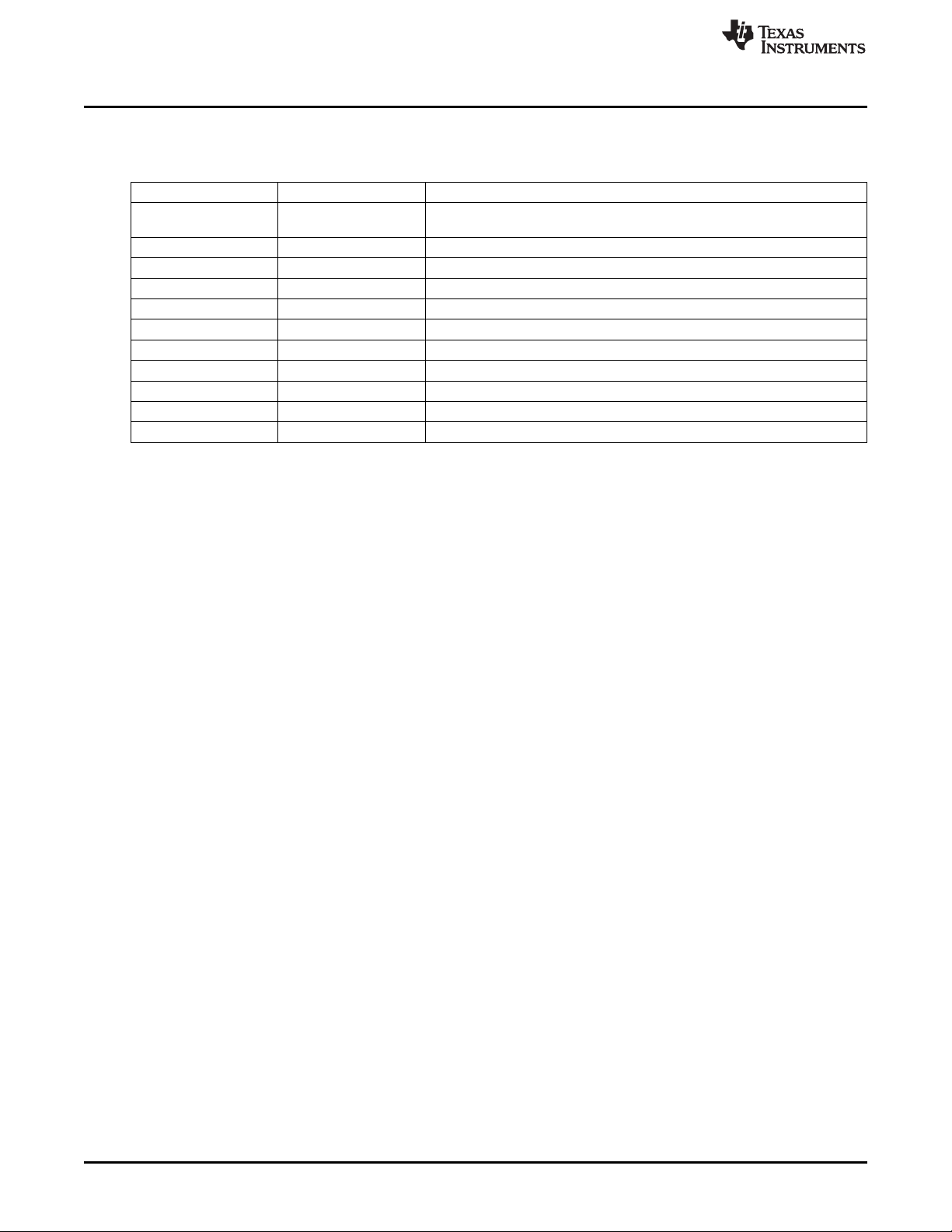
Electrical Performance Specifications
3 Electrical Performance Specifications
Table 1. UCC28610EVM-474 Electrical Performance Specifications
PARAMETER CONDITIONS MIN NOM MAX UNITS
INPUT CHARACTERISTICS
V
IN
I
IN
V
UVLO
OUTPUT CHARACTERISTICS
V
OUT
V
ripple
I
OUT
I
OCP
V
OVP
SYSTEM CHARACTERISTICS
f
SW
h
PEAK
MECHANICAL CHARACTERISTICS
Width Dimensions 2.3
Length 3.5 inches
Height Component height 1
Input voltage 85 265 VRMS
Input current VIN= 115 V
VIN= 115 V
Brown out I
OUT
RMS
RMS
= max 72 V
Output voltage VIN= min to max, I
Output voltage ripple VIN= 115 V
RMS
Output current VIN= min to max 0 2.1 A
Output over current VIN= max
inception point
Output OVP I
Transient response voltage I
over shoot
= min to max 16 V
OUT
= min to max
OUT
Switching frequency 26.3 140.4 kHz
Peak efficiency VIN= 115 V
No load power consumption VIN= 115 V
VIN= 230 V
RMS
RMS
RMS
Operating temperature VIN= min to max, I
range
, I
= max 0.3 A
OUT
, I
= 0 A 0.03 A
OUT
= min to max 10.8 12 13.2 V
OUT
, I
= max 80 120 mVpp
OUT
3 A
500 mV
, I
= 1.05 A 85.7 %
OUT
67
107
= min to max
OUT
25 °C
www.ti.com
mW
4
UCC28610EVM-474 25-W Universal Off-Line Flyback Converter SLUU383B–November 2009– Revised May 2011
Copyright © 2009–2011, Texas Instruments Incorporated
Submit Documentation Feedback
Page 5
T
INSTRUMENTS
EXAS
www.ti.com
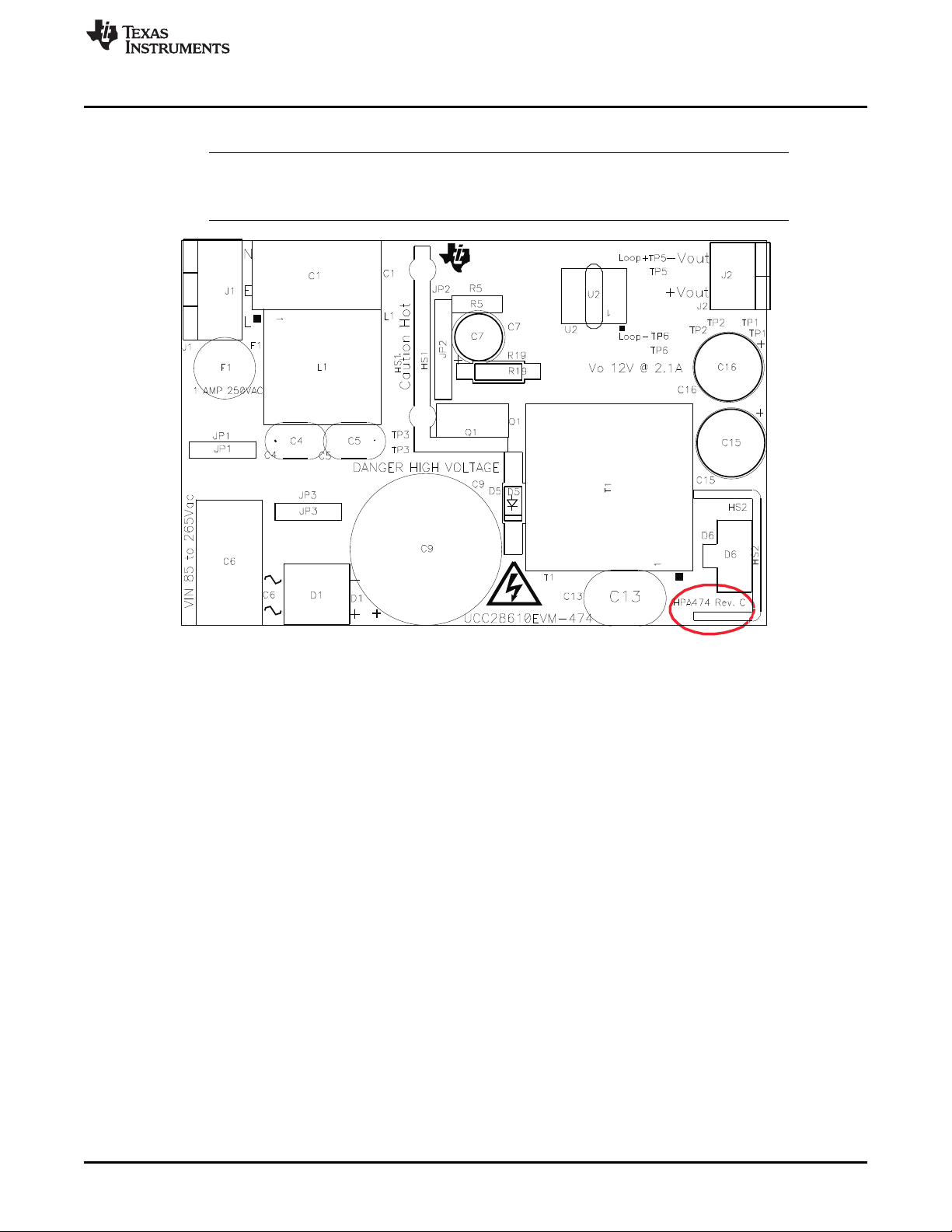
4 Schematic/Revision Code Placement
NOTE: For revision A versions of the evaluation module, please refer to Appendix A of this user's
guide for the schematic, list of materials and board layout. The EVM revision code can be
found on the lower right corner of the top side of the board, as shown in Figure 1.
Schematic/Revision Code Placement
Figure 1. Placement of Revision Code for the Evaluation Module.
SLUU383B–November 2009– Revised May 2011 UCC28610EVM-474 25-W Universal Off-Line Flyback Converter
Submit Documentation Feedback
Copyright © 2009–2011, Texas Instruments Incorporated
5
Page 6
+
+
+
+
Schematic/Revision Code Placement
www.ti.com
Figure 2. UCC28610EVM-474 Schematic
6
UCC28610EVM-474 25-W Universal Off-Line Flyback Converter SLUU383B–November 2009– Revised May 2011
Copyright © 2009–2011, Texas Instruments Incorporated
Submit Documentation Feedback
Page 7

www.ti.com
4.1 Circuit Description
A brief description of the circuit elements follows:
• Diode bridge D1, input capacitor C9, transformer (a.k.a. flyback inductor) T1, HV MOSFET Q1,
UCC28610 controller U1, Schottky rectifier D6, Output capacitors C15 and C16 form the power stage
of the converter. Note that the UCC28610 U1 is part of the power stage. This is because the DRV and
GND pins carry the full peak primary side current of the converter.
• Capacitors C12, C14, and C17 filter the high frequency noise directly across the electrolytic input and
output capacitors.
• The input EMI filter is made up of X2 capacitors, C1 and C6, and common mode inductor L1 and Y2
capacitors, C4 and C5. Excessive surge current protection is provided by a slow blow fuse, F1.
• Resistor R11, capacitor C11, and diode D5 make up the primary side voltage clamp for the HV
MOSFET. The clamp prevents the drain voltage on Q1 from exceeding its maximum rating. The
integrated snubber, composed of R12 and C11, reduces the ringing on the primary side windings that
might inadvertently trigger the zero current detection circuit in the device.
• Resistors R7, R8, and R9 supply start up bias current to the VGG shunt regulator. Schottky diode D3
is required to provide initial start up to VDD from VGG at start up.
• Operating bias to the controller is provided by the auxiliary winding on T1, diode D2, and bulk capacitor
C7. The zener diode, D4, maintains the bias voltage on VDD below the absolute maximum rating at full
load.
• Gate drive circuitry is composed of gate drive resistor R10, used for damping oscillations during turn
on. Resistor R16 and diode D8 are required to provide a current path at turn off because the gate is
shorted to the source of the HV MOSFET during each switching cycle. For circuits that experience high
ringing on VGG at turn off, R16 can be replaced with a ferrite bead.
• Capacitors C8 and C10 are decoupling capacitors which should always be good quality low ESR/ESL
type capacitors placed as close to the device pins as possible and returned directly to the device
ground reference.
• C13 filters the common mode noise between the primary and secondary sides.
• Inductor L2, with capacitor C16, reduces the output voltage ripple.
• Resistors R5 and R3 program the over voltage threshold. Capacitor C3 can be used to add a small
delay to ZCD, to align the turn on time of the primary switch with the resonant valley of the primary
winding.
• Resistor R6 programs the maximum on time of the HV MOSFET.
• Resistor R4 sets the maximum value for the peak primary current.
• Resistor R2 and capacitor C2 provide a filter for the FB signal while resistor R1 ensures that the
optocoupler emitter current can go to 0A. Resistor R19 provides a non-intrusive point to monitor the FB
by measuring the voltage drop across R19.
• The simple output voltage feedback loop is composed of zener diode D7, resistors R14 and R15, and
the optocoupler U2. Using an opto with a low CTR provides better noise immunity. Resistor R13 is
used as an injection point for small signal frequency response testing.
Schematic/Revision Code Placement
SLUU383B–November 2009– Revised May 2011 UCC28610EVM-474 25-W Universal Off-Line Flyback Converter
Submit Documentation Feedback
Copyright © 2009–2011, Texas Instruments Incorporated
7
Page 8

EVM Test Set Up
5 EVM Test Set Up
Figure 2 shows the equipment set up when measuring the input power consumption during no load. Note
the addition of the 10-Ω shunt resistor in Figure 3. During the no-load test, the power analyzer should be
set for long averaging in order to include several cycles of operation and an appropriate current scale
factor for using the external shunt must be used. Figure 3 shows the basic test set up recommended to
evaluate the UCC28610EVM-474 with a load.
High voltages that may cause injury exist on this evaluation
module (EVM). Please ensure all safety procedures are followed
when working on this EVM. Never leave a powered EVM
unattended.
5.1 Test Equipment
See Figure 3 and Figure 4 for recommended test set ups.
• AC Input Source: The input source shall be an isolated variable AC source capable of supplying
between 85 V
Figure 4. For accurate efficiency calculations, a power meter should be inserted between the neutral
line of the AC source and the Neutral terminal of the EVM. For highest accuracy, connect the voltage
terminals of the power meter directly across the Line and Neutral terminals of the EVM.
• Load: For the output load, a programmable electronic load set to constant current mode and capable
of sinking 0 to 3 ADCat 12 VDCshall be used. For highest accuracy, V
connecting a DC voltmeter, DMM V1, directly across the +Vout and –Vout terminals as shown in
Figure 3 and Figure 4. A DC current meter, DMM A1, should be placed in series with the electronic
load for accurate output current measurements.
• Power Meter: The power analyzer shall be capable of measuring low input current, typically less than
10 mA, and a long averaging mode if low power standby mode input power measurements are to be
taken. An example of such an analyzer is the Voltech PM100 Single Phase Power Analyzer. To
measure the intermittent bursts of current and power drawn from the line during no-load operation, an
external 10-Ω shunt, with a current scale factor of 10 A/V, was used at a high sample rate over an
extended period of time in order to display the averaged results (refer to Figure 3).
• Multimeters: Two digital multimeters are used to measure the regulated output voltage (DMM V1) and
load current (DMM A1).
• Oscilloscope: A digital or analog oscilloscope with a 500-MHz scope probe is recommended.
• Fan: Forced air cooling is not required.
• Recommended Wire Gauge: a minimum of AWG18 wire is recommended. The wire connections
between the AC source and the EVM , and the wire connections between the EVM and the load
should be less than two feet long.
RMS
and 265 V
WARNING
at no less than 30 W and connected as shown in Figure 3 and
RMS
can be monitored by
OUT
www.ti.com
8
UCC28610EVM-474 25-W Universal Off-Line Flyback Converter SLUU383B–November 2009– Revised May 2011
Copyright © 2009–2011, Texas Instruments Incorporated
Submit Documentation Feedback
Page 9
T
I
NSTRUMENTS
EXAS
AC SOURCE
Line
Neutral
DMM V
1
+ -
Oscilloscope
POWER METER
V
HI
VLOA
HI
A
LO
A
EXT
+ +
-
-
10
AC SOURCE
LineNeutral
DMM A
1
+ -
DMM V
1
+ -
Oscilloscope
ELECTRONIC
LOAD
+
-
POWER METER
V
HI
VLOA
HI
A
LO
A
EXT
+ +
--
T
I
NSTRUMENTS
EXAS
www.ti.com
5.2 Recommended Test Set Up for Operation Without a Load
EVM Test Set Up
Figure 3. UCC28610EVM-474 Recommended Test Set Up Without a Load
5.3 Recommended Test Set Up for Operation With a Load
SLUU383B–November 2009– Revised May 2011 UCC28610EVM-474 25-W Universal Off-Line Flyback Converter
Submit Documentation Feedback
Figure 4. UCC28610EVM-474 Recommended Test Set Up With a Load
Copyright © 2009–2011, Texas Instruments Incorporated
9
Page 10
EVM Test Set Up
5.4 List of Test Points
TEST POINT NAME DESCRIPTION
TP1 +Vout
TP2 -Vout Return of the output of the EVM, secondary side GND reference.
TP3 Pwr RTN Primary side power ground
TP4 QGND Primary side signal ground
TP5 +LOOP Loop injection point, EVM output
TP6 -LOOP Loop injection point
J1-1 Neutral Neutral input from the AC source
J1-2 Earth Earth reference from the AC source
J1-3 AC Line Line input from AC source
J2-1 +Vout Positive output terminal of the EVM to the load
J2-2 -Vout Return connection of the EVM output to the load
www.ti.com
Table 2. Test Point Functional Description
Output voltage of EVM; this designator is not populated with a pin in order to
facilitate tip and barrel output ripple voltage measurements.
10
UCC28610EVM-474 25-W Universal Off-Line Flyback Converter SLUU383B–November 2009– Revised May 2011
Copyright © 2009–2011, Texas Instruments Incorporated
Submit Documentation Feedback
Page 11

www.ti.com
6 Test Procedure
All tests should use the set up as described in Section 5 of this user’s guide. The following test procedure
is recommended primarily for power up and shutting down the evaluation module. Never leave a powered
EVM unattended for any length of time.
6.1 Applying Power to the EVM
1. Set up the EVM as shown in Section 5 of this user’s guide
(a) If no-load input power measurements are to be made, set the power analyzer to long averaging
and external shunt mode. Insert a shunt, such as a 10-Ω resistor as shown in Figure 3, in series
with the Neutral terminal of the EVM. Set the appropriate current scale on the power analyzer.
(b) For operation with a load, as shown in Figure 4, set the electronic load to constant current mode to
sink 0 A.
2. Prior to turning on the AC source, set the voltage to between 85 VACand 265 VAC.
3. Turn on the AC source.
4. Monitor the output voltage on DMM V1.
5. Monitor the output current on DMM A1.
6. The EVM is now ready for testing.
6.2 No-Load Power Consumption
1. Use the test set up shown in Figure 3.
(a) Set the power analyzer to external shunt mode.
(b) Set the appropriate current scale factor for using an external shunt on the power analyzer. A 10-Ω
shunt scales at 10,000 mV/A for the PM100 Voltech.
(c) Set the power analyzer long averaging time to include several cycles of operation. The PM100
Voltech should be set to a long averaging time of 10 or more for accurate burst mode
measurements.
2. Apply power to the EVM per Section 6.1.
3. Monitor the input power on the power analyzer while varying the input voltage.
4. Make sure the input power is off and the bulk capacitor and output capacitors are completely
discharged before handling the EVM.
Test Procedure
SLUU383B–November 2009– Revised May 2011 UCC28610EVM-474 25-W Universal Off-Line Flyback Converter
Submit Documentation Feedback
Copyright © 2009–2011, Texas Instruments Incorporated
11
Page 12

Test Procedure
6.3 Output Voltage Regulation and Efficiency
1. For load regulation:
(a) Use the test set up shown in Figure 4.
(i) Be sure to remove the external shunt from the power analyzer and set the analyzer to normal
mode (not long averaging).
(b) Set the AC source to a constant voltage between 85 VACand 265 VAC.
(c) Apply power to the EVM per Section 6.1.
(d) Vary the load current from 0 A up to 2.1 A, as measured on DMM A1.
(e) Observe that the output voltage on DMM V1remains within 10% of 12 VDC.
2. For line regulation:
(a) Set the load to sink 2.1 A.
(b) Vary the AC source from 85 VACto 265 VAC.
(c) Observe that the output voltage on DMM V1remains within 10% of 12 VDC.
3. Make sure the input power is off and the bulk capacitor and output capacitors are completely
discharged before handling the EVM.
6.4 Output Voltage Ripple
1. Expose the ground barrel of the scope probe. Insert the tip of the probe into the plated via located on
the +Vout pad of the EVM (TP1) and lean the probe so that the exposed ground barrel is resting on the
test point on the –Vout pad of the EVM (TP2) for a tip and barrel measurement as shown in the
example depicted in Figure 5.
2. Apply power to the EVM per Section 6.1.
3. Monitor the output voltage ripple on the oscilloscope.
www.ti.com
Figure 5. Typical Example of Tip and Barrel Measurement Technique
NOTE: This photo was not taken on the UCC28610EVM specifically but serves as a visual aid to
perform the test measurement.
6.5 Equipment Shutdown
1. Ensure the load is at maximum; this will quickly discharge the output capacitors.
2. Turn off the AC source.
12
UCC28610EVM-474 25-W Universal Off-Line Flyback Converter SLUU383B–November 2009– Revised May 2011
Copyright © 2009–2011, Texas Instruments Incorporated
Submit Documentation Feedback
Page 13

EFFICIENCY vs. LOAD CURRENT
0.800
0.810
0.820
0.830
0.840
0.850
0.860
0.870
0.5 0.7 0.9 1.1 1.3 1.5 1.7 1.9 2.1 2.3
LOA D(A)
E F FI C IE N C Y
85VAC
115VAC
230VAC
264VAC
No-Load Power Consumption vs. Line Voltage
265Vac
230Vac
85Vac
115Vac
0
20
40
60
80
100
120
140
80 100 120 140 160 180 200 220 240 260 280
Line Voltage (Vac)
In p u t P o w e r ( m W )
www.ti.com
Performance Data and Typical Characteristic Curves
7 Performance Data and Typical Characteristic Curves
Figure 6 through Figure 23 present typical performance curves for the UCC28610EVM-474.
Figure 6. Efficiency as a Function of Load Current and Input Voltage
Figure 7. No-Load Input Power as a Function of Input Voltage
SLUU383B–November 2009– Revised May 2011 UCC28610EVM-474 25-W Universal Off-Line Flyback Converter
Submit Documentation Feedback
Copyright © 2009–2011, Texas Instruments Incorporated
13
Page 14

FB CURRENTvs. DRV CURRENT
0
200
400
600
800
1000
1200
1400
1600
1800
0 50 100 150 200 250 300 350
IFB (uA)
ID R V ( m A )
85Vac
115Vac
230Vac
265Vac
FB CURRENT vs. SWITCHING FREQUENCY
0
20
40
60
80
100
120
140
0 50 100 150 200 250 300 350
IFB(uA)
F sw ( k H z)
85Vac
115Vac
230Vac
265Vac
Performance Data and Typical Characteristic Curves
www.ti.com
Figure 8. DRV Current as a Function of FB Current
Figure 9. Switching Frequency as a Function of FB Current
14
UCC28610EVM-474 25-W Universal Off-Line Flyback Converter SLUU383B–November 2009– Revised May 2011
Copyright © 2009–2011, Texas Instruments Incorporated
Submit Documentation Feedback
Page 15

OUTPUT VOLTAGEvs LOADCURRENT
10.8
11.3
11.8
12.3
12.8
0 0.5 1 1.5 2 2.5 3
LOAD CURRENT (A)
O U T P U T V O L T A G E ( V)
85Vac
115Vac
230Vac
265Vac
www.ti.com
Performance Data and Typical Characteristic Curves
Figure 10. Output Voltage as a Function of Load Current and Line Voltage
(Note the shutdown/retry threshold for each line voltage.)
Figure 11. Start-Up Waveform
(Input voltage = 115 VAC, full load. Ch.1 = bulk input voltage, 100 V/div., Ch.2 = VGG, 10 V/div., Ch.3 =
VDD, 10V/div., Ch.4 = DRV, 10V/div.)
SLUU383B–November 2009– Revised May 2011 UCC28610EVM-474 25-W Universal Off-Line Flyback Converter
Submit Documentation Feedback
Copyright © 2009–2011, Texas Instruments Incorporated
15
Page 16

Performance Data and Typical Characteristic Curves
www.ti.com
Figure 12. FM Mode Switching Cycle Waveform
(Input voltage = 115 VAC, full load, fSW= 112 kHz. Ch.1 = I
MOSFET, 100 V/div., Ch.3 = ZCD, 5 V/div.)
, 500 mA/div., I
DRV
= 1.53 A, Ch.2 = Drain of HV
DRV
Figure 13. AM Mode Switching Cycle Waveform
(Input voltage = 85 VAC, 0.3-A load, fSW= 28.2 kHz, Ch.1 = I
MOSFET, 100 V/div., Ch.3 = ZCD, 5 V/div., Ch. 4 = VDD, 10 V/div.)
16
UCC28610EVM-474 25-W Universal Off-Line Flyback Converter SLUU383B–November 2009– Revised May 2011
Copyright © 2009–2011, Texas Instruments Incorporated
, 500 mA/div., I
DRV
= 1.1 A, Ch.2 = Drain of HV
DRV
Submit Documentation Feedback
Page 17

www.ti.com
Performance Data and Typical Characteristic Curves
Figure 14. GM Mode Switching Cycle Waveform
(Input voltage = 85 VAC, 0-A load, fSW= 28 kHz, Ch.1 = I
MOSFET, 100 V/div., Ch.3 = ZCD, 5 V/div., Ch. 4 = VDD, 10 V/div.)
, 500 mA/div., I
DRV
= 440 mA, Ch.2 = Drain of HV
DRV
Figure 15. Ripple on VGG and VDD During Green Mode Operation
(Ch.3 = VGG, AC coupled, 2 V/div., Ch.4 = VDD, AC coupled, 200 mV/div.)
SLUU383B–November 2009– Revised May 2011 UCC28610EVM-474 25-W Universal Off-Line Flyback Converter
Submit Documentation Feedback
Copyright © 2009–2011, Texas Instruments Incorporated
17
Page 18

Performance Data and Typical Characteristic Curves
www.ti.com
Figure 16. Output Voltage Ripple During Green Mode Operation
(Input voltage = 85 VAC, no load. Ch.2 = V
, AC coupled, 20 mV/div.)
OUT
18
Figure 17. Output Voltage Ripple During Frequency Modulation Mode
(Input voltage = 85 VAC, full load. Ch.2 = V
UCC28610EVM-474 25-W Universal Off-Line Flyback Converter SLUU383B–November 2009– Revised May 2011
Copyright © 2009–2011, Texas Instruments Incorporated
, AC coupled, 20 mV/div.)
OUT
Submit Documentation Feedback
Page 19

www.ti.com
Performance Data and Typical Characteristic Curves
Figure 18. Load Transient, 0% to 100% Load Step
(Ch.1 = I
, 2 A/div., Ch.2 = V
OUT
, AC coupled, 200 mV/div.)
OUT
Figure 19. Brown-Out Protection
(MOT shutdown/retry response triggered at full load when input voltage dropped to 72.4 VAC. Note the
750-ms t
SLUU383B–November 2009– Revised May 2011 UCC28610EVM-474 25-W Universal Off-Line Flyback Converter
Submit Documentation Feedback
RETRY
. Ch.1 = I
Copyright © 2009–2011, Texas Instruments Incorporated
, Ch.3 = VDD, 10 V/div., Ch.4 = VGG, 10 V/div.)
DRV
19
Page 20

Performance Data and Typical Characteristic Curves
www.ti.com
Figure 20. Output Short Circuit Protection
(Short circuit maintained on output; note the output current goes to 4.62 A, refer to equation 13 in the
data sheet, during the 250-ms delay to overload fault, tOL, and retries after t
85 VAC. Ch.1 = I
, 1 A/div., Ch. 3 = V
OUT
, 1 V/div.)
OUT
= 750 ms. Input voltage =
RETRY
Figure 21. Output Over Voltage Protection
(The EVM was tested with an open FB loop, no load. OVP threshold is equal to 15.44 V. Ch. 3 = V
V/div., offset by 4 V.)
20
UCC28610EVM-474 25-W Universal Off-Line Flyback Converter SLUU383B–November 2009– Revised May 2011
Copyright © 2009–2011, Texas Instruments Incorporated
Submit Documentation Feedback
OUT
, 2
Page 21

115Vac Bode Plot
-60
-40
-20
0
20
40
60
100 1000 10000
Frequen cy (Hz)
G a in (d B )
-180
-120
-60
0
60
120
180
P h a s e ( d e g r e es )
Gain Phase
230Vac Bode Plot
-60
-40
-20
0
20
40
60
100 1000 10000
Frequency (Hz)
G a i n (d B )
-180
-120
-60
0
60
120
180
P h a s e ( d e g r e e s)
Gain Phase
www.ti.com
Performance Data and Typical Characteristic Curves
Figure 22. Bode Plot (Input voltage = 115 VAC, full load.)
Figure 23. Bode Plot (Input voltage = 230 VAC, full load.)
SLUU383B–November 2009– Revised May 2011 UCC28610EVM-474 25-W Universal Off-Line Flyback Converter
Submit Documentation Feedback
Copyright © 2009–2011, Texas Instruments Incorporated
21
Page 22

T
INSTRUMENTS
EXAS
EVM Assembly Drawing and Layout
8 EVM Assembly Drawing and Layout
Figure 24 through Figure 26 show the design of the UCC28610EVM-474 printed circuit board.
www.ti.com
Figure 24. Top Layer Component Placement
22
UCC28610EVM-474 25-W Universal Off-Line Flyback Converter SLUU383B–November 2009– Revised May 2011
Copyright © 2009–2011, Texas Instruments Incorporated
Submit Documentation Feedback
Page 23

Figure 28. Bottom Layer Component Placement.
www.ti.com
EVM Assembly Drawing and Layout
Figure 25. Bottom Layer Routing
Figure 26. Bottom Layer Component Placement
SLUU383B–November 2009– Revised May 2011 UCC28610EVM-474 25-W Universal Off-Line Flyback Converter
Submit Documentation Feedback
Copyright © 2009–2011, Texas Instruments Incorporated
23
Page 24

List of Materials
9 List of Materials
COUNT REF DES DESCRIPTION PART NUMBER MFR
2 C1, C6 ECQ-U2A334ML Panasonic
1 C2 Capacitor, ceramic, 100 pF, 50 V, NP0, ±5%, 0603 Std Std
C3 Capacitor, ceramic, not populated, 50 V, NP0, ±5%,
0 Std Std
C4, C5 Capacitor, ceramic, 2200 pF, 250 VAC, X1/Y2, ±20%,
2 DE2E3KY222MA2BM01 muRata
(optional) 0.315 x 0.200 inch
1 C7 EEU-FC1V680 Panasonic
1 C8 Capacitor, ceramic, 0.1 µF, 50 V, X7R, ±10%, 0805 CC0805KRX7R9BB104 Yageo Corporation
1 C9 EET-HC2G101BA Panasonic
1 C10 Capacitor, ceramic, 0.1 µF, 100 V, X7R, ±10%, 1206 Std Std
1 C11 Std Std
1 C12 Capacitor, ceramic, 0.1 µF, 630 V, X7R, ±10%, 1812 C4532X7R2J104K TDK Corporation
1 C13 ECK-ANA102MB Panasonic
2 C14, C17 Capacitor, ceramic, 1 µF, 25 V, X5R, ±10%, 0805 Std Std
2 C15, C16 EEU-FM1E681 Panasonic
1 D1 Diode, bridge, 1 A, 600 V DF06M Diodes Inc.
1 D2 Diode, ultra fast, 1 A, 200 V, SMA MURA120T3G On Semiconductor
1 D3 Diode, schottky, 100 mA, 40 V, SOD-323 RB501V-40TE-17
1 D4 Diode, Zener, 25 V, 500 mW, SOD-123 MMSZ5253BT1G On Semiconductor
1 D5 UF4007-TP
1 D6 Diode, dual Schottky, 20 A, 100 V, TO-220 STPS20H100CT STMicroelectronics
1 D7 Diode, Zener, 10 V, 500 mW, SOD-123 MMSZ5240B
1 D8 Diode, Schottky barrier, 1 A, 30 V, SMini2-F2 MA21D3400L Panasonic - SSG
1 F1 Fuse, slow blow, 1 A, 250 V, 0.335 inch 38211000410
1 HS1 Heatsink, TO-220, vertical-mount, 0.5 x 0.750 inch 507302B00000 Aavid Thermalloy
1 HS2 Heatsink, alloy 1110 copper, 0.530 x 1.200 inch HS001 NH Stamp
1 L1 54P512-276
1 L2 HCP0703-3R3-R Coiltronics/Cooper
1 Q1 MOSFET, Nch, 600 V, 6 A, SC-67 2SK3562 Toshiba
www.ti.com
Table 3. List of Materials for UCC28610EVM-474
Capacitor, film, 0.33 µF, 275 VAC, X2, ±20%, 0.690 x
0.374 inch
0603
Capacitor, aluminum electrolytic, 68 µF, 35 V, ±20%,
0.200 inch
Capacitor, aluminum electrolytic, 100 µF, 400 VDC,
±20%, 25 x 20 mm
Capacitor, ceramic, 330 pF, 630 V, C0G, NP0, ±5%,
1206
Capacitor, ceramic disk, 1000 pF, 250 V, Y1/X1, ±20%,
0.394 x 0.315 inch
Capacitor, aluminum electrolytic, 680 µF, 25 V, ±20%,
10 x 25 mm
Rohm
Semiconductor
Diode, fast recovery glass passivated, 1 A, 1 kV, Micro Commercial
DO-41 Co.
Fairchild
Semiconductor
Littelfuse /
Wickmann
Inductor, AC line, common choke, 2 7 mH, 1 A, 0.660 x Vitec Electronics
0.670 inch Corp.
Inductor, high current choke, 3.3 µH, 0.276 x 0.288
inch
24
UCC28610EVM-474 25-W Universal Off-Line Flyback Converter SLUU383B–November 2009– Revised May 2011
Copyright © 2009–2011, Texas Instruments Incorporated
Submit Documentation Feedback
Page 25

www.ti.com
References
Table 3. List of Materials for UCC28610EVM-474 (continued)
COUNT REF DES DESCRIPTION PART NUMBER MFR
1 R1 Resistor, chip, 100 kΩ, 1/10 W, ±1%, 0603 Std Std
1 R2 Resistor, chip, 20.5 kΩ, 1/10 W, ±1%, 0603 Std Std
1 R3 Resistor, chip, 51.1 kΩ, 1/10 W, ±1%, 0603 Std Std
1 R4 Resistor, chip, 64.9 kΩ, 1/10 W, ±1%, 0603 Std Std
1 R5 SFR16S0001693FR500
1 R6 Resistor, chip, 68.1 kΩ, 1/10 W, ±1%, 0603 Std Std
R7, R8,
3 Resistor, chip, 2.05MΩ, 1/8 W, 150V, ±1%, 0805 CRCW08052M05FKEA Vishay/Dale
R9
1 R10 Resistor, chip, 15.4 Ω, 1/8 W, ±1%, 0805 Std Std
1 R11 Resistor, chip, 64.9 kΩ, 1/2 W, ±1%, 2010 Std Std
1 R12 Resistor, chip, 33.2 Ω, 1 W, ±5%, 2512 Std Std
1 R13 Resistor, chip, 20.5 Ω, 1/10 W, ±1%, 0603 Std Std
1 R14 Resistor, chip, 1.00 kΩ, 1/10 W, ±1%, 0603 Std Std
1 R15 Resistor, chip, 681 Ω, 1/10 W, ±1%, 0603 Std Std
1 R16 Resistor, chip, 0 Ω, 1/10 W, ±1%, 0603 Std Std
1 R19 Resistor, metal film, 1.00 kΩ, 1/4 W, ±1%, TH-400 Std Std
1 T1 Transformer, flyback, 220 µH, PQ20/20 58P6936 Vitec Electronics
1 U1 Green-mode flyback controller, SO-8 UCC28610D Texas Instruments
1 U2 CNY17F1M
Resistor, metal film, 169 kΩ, 1/2 W, ±1%, 0.300 x Vishay/BC
0.100 inch Components
Optocoupler, CTR 40% - 80%, 70 Vceo, 5000 V
DIP6 Optoelectronics
, Fairchild
RMS
10 References
1. UCC28610 Green-Mode Flyback Controller, Datasheet, (TI Literature Number SLUS888)
2. Standby and Low Power Measurements, VOLTECHNOTES, VPN 104-054/1,
http://www.voltech.com/Downloads/PMAppNotes/Low%20Power%20Standby.pdf
SLUU383B–November 2009– Revised May 2011 UCC28610EVM-474 25-W Universal Off-Line Flyback Converter
Submit Documentation Feedback
Copyright © 2009–2011, Texas Instruments Incorporated
25
Page 26

+
+
+
+
Appendix A
A.1 UCC28610EVM-474 Rev. A
The following schematic, board layout, and list of materials apply to the UCC28610EVM-474 Rev. A
version of the evaluation module. The Rev. A version of the EVM includes differential mode inductors L2
and L3. Subsequent revisions of the EVM replaced these inductors with a short circuit.
www.ti.com
26
Figure 27. UCC28610EVM-474 Rev. A Schematic
SLUU383B–November 2009– Revised May 2011
Copyright © 2009–2011, Texas Instruments Incorporated
Submit Documentation Feedback
Page 27

T
I
NSTRUMENTS
EXAS
www.ti.com
UCC28610EVM-474 Rev. A
Figure 28. Top Side View of UCC28610EVM-474 Rev. A
Figure 29. Top Layer Component Placement for UCC28610EVM-474 Rev. A
SLUU383B–November 2009– Revised May 2011
Submit Documentation Feedback
Copyright © 2009–2011, Texas Instruments Incorporated
27
Page 28

UCC28610EVM-474 Rev. A
www.ti.com
Figure 30. Bottom Layer Routing of UCC28610EVM-474 Rev. A
Figure 31. Bottom Layer Component Placement of UCC28610EVM-474 Rev. A
28
SLUU383B–November 2009– Revised May 2011
Submit Documentation Feedback
Copyright © 2009–2011, Texas Instruments Incorporated
Page 29

www.ti.com
UCC28610EVM-474 Rev. A
Table 4. Table 4. List of Materials for UCC28610EVM-474 Rev. A
COUNT REF DES DESCRIPTION PART NUMBER MFR
2 C1, C6 ECQ-U2A334ML Panasonic
1 C2 Capacitor, ceramic, 100 pF, 50 V, NP0, ±5%, 0603 Std Std
0 C3 Capacitor, ceramic, not populated, 50 V, NP0, ±5%, 0603 Std Std
C4, C5 Capacitor, ceramic, 2200 pF, 250 VAC, X1/Y2, ±20%, DE2E3KY222MA2BM
2 muRata
(optional) 0.315 x 0.200 inch 01
1 C7 EEU-FC1V680 Panasonic
1 C8 Capacitor, ceramic, 0.1 µF, 50 V, X7R, ±10%, 0805 Yageo Corporation
1 C9 EET-HC2G101BA Panasonic
1 C10 Capacitor, ceramic, 0.1 µF, 100 V, X7R, ±10%, 1206 Std Std
1 C11 Capacitor, ceramic, 330 pF, 630 V, C0G, NP0, ±5%, 1206 Std Std
1 C12 Capacitor, ceramic, 0.1 µF, 630 V, X7R, ±10%, 1812 C4532X7R2J104K TDK Corporation
1 C13 ECK-ANA102MB Panasonic
2 C14, C17 Capacitor, ceramic, 1 µF, 25 V, X5R, ±10%, 0805 Std Std
2 C15, C16 EEU-FM1E681 Panasonic
1 D1 Diode, bridge, 1 A, 600 V DF06M Diodes Inc.
1 D2 Diode, ultra fast, 1 A, 200 V, SMA MURA120T3G On Semiconductor
1 D3 Diode, Schottky, 100 mA, 40 V, SOD-323 RB501V-40TE-17 Rohm Semiconductor
1 D4 Diode, Zener, 500 mW, 25 V, SOD-123 MMSZ5253BT1G On Semiconductor
1 D5 Diode, fast recovery glass passivated, 1 A, 1 kV, DO-41 UF4007-TP Micro Commercial Co.
1 D6 Diode, dual Schottky, 20 A, 100 V, TO-220 STPS20H100CT STMicroelectronics
1 D7 Diode, Zener, 10 V, 500 mW, SOD-123 MMSZ5240B
1 D8 Diode, Schottky barrier, 1 A, 30 V, SMini2-F2 MA21D3400L Panasonic - SSG
1 F1 Fuse, slow blow, 1 A, 250 V, 0.335 inch 38211000410 Littelfuse / Wickmann
1 HS1 Heatsink, TO-220, vertical mount, 0.5 x 0.750 inch 507302B00000 Aavid Thermalloy
1 HS2 Heatsink, alloy 1110 copper, 0.530 x 1.200 inch HS001 NH Stamp
1 L1 54P512-276
2 L2, L3 Inductor, EMI, 723 µH, 0.620 Ω, ±15%, 11.94 x 15.49 mm 54P2986
1 L4 Inductor, high current choke, 3.3 µH, 0.276 x 0.288 inch HCP0703-3R3-R Coiltronics/Cooper
1 Q1 MOSFET, N-channel, 600 V, 6A, SC-67 2SK3562 Toshiba
Capacitor, film, 0.33 µF, 275VAC, X2, ±20%, 0.690 x
0.374 inch
Capacitor, aluminum electrolytic, 68 µF, 35 V, ±20%,
0.200 inch
CC0805KRX7R9BB10
4
Capacitor, aluminum electrolytic, 100 µF, 400 VDC, ±20%,
25 x 20 mm
Capacitor, ceramic disk, 1000 pF, 250 V, Y1/X1, ±20%,
0.394 x 0.315 inch
Capacitor, aluminum electrolytic, 680 µF, 25 V, ±20%, 10
x 25 mm
Fairchild
Semiconductor
Inductor, AC line, common choke, 27 mH, 1 A, 0.660 x Vitec Electronics
0.670 inch Corp.
Vitec Electronics
Corp.
SLUU383B–November 2009– Revised May 2011
Submit Documentation Feedback
Copyright © 2009–2011, Texas Instruments Incorporated
29
Page 30

UCC28610EVM-474 Rev. A
Table 4. Table 4. List of Materials for UCC28610EVM-474 Rev. A (continued)
COUNT REF DES DESCRIPTION PART NUMBER MFR
1 R1 Resistor, chip, 100 kΩ, 1/10 W, ±1%, 0603 Std Std
1 R2 Resistor, chip, 20.5 kΩ, 1/10 W, ±1%, 0603 Std Std
1 R3 Resistor, chip, 51.1 kΩ, 1/10 W, ±1%, 0603 Std Std
1 R4 Resistor, chip, 64.9 kΩ, 1/10 W, ±1%, 0603 Std Std
1 R5
1 R6 Resistor, chip, 68.1 kΩ, 1/10 W, ±1%, 0603 Std Std
R7, R8, CRCW08052M05FKE
3 Resistor, chip, 2.05 MΩ, 1/8 W, 150 V, ±1%, 0805 Vishay/Dale
R9 A
1 R10 Resistor, chip, 15.4 W, 1/8 W, ±1%, 0805 Std Std
1 R11 Resistor, chip, 64.9 kΩ, 1/2 W, ±1%, 2010 Std Std
1 R12 Resistor, chip, 33.2 Ω, 1 W, ±5%, 2512 Std Std
1 R13 Resistor, chip, 20.5 Ω, 1/10 W, ±1%, 0603 Std Std
1 R14 Resistor, chip, 1.00 kΩ, 1/10 W, ±1%, 0603 Std Std
1 R15 Resistor, chip, 681 Ω, 1/10 W, ±1%, 0603 Std Std
1 R16 Resistor, chip, 0 Ω, 1/10 W, ±1%, 0603 Std Std
1 R19 Resistor, metal film, 1.00 kΩ, 1/4 W, ±1%, TH-400 Std Std
1 T1 Transformer, flyback, 220 µH, PQ20/20 58P6936 Vitec Electronics
1 U1 Green-Mode Flyback Controller, SO-8 UCC28610D Texas Instruments
1 U2 Optocoupler, CTR 40% - 80%, 70 Vceo, 5000Vrms, DIP6 CNY17F1M
www.ti.com
Resistor, metal film, 169 kΩ, 1/2 W, ±1%, 0.300 x 0.100 SFR16S0001693FR5 Vishay/BC
inch 00 Components
Fairchild
Optoelectronics
30
SLUU383B–November 2009– Revised May 2011
Copyright © 2009–2011, Texas Instruments Incorporated
Submit Documentation Feedback
Page 31

www.ti.com
UCC28610EVM-474 Rev. A
EVALUATION BOARD/KIT IMPORTANT NOTICE
Texas Instruments (TI) provides the enclosed product(s) under the following conditions:
This evaluation board/kit is intended for use for ENGINEERING DEVELOPMENT, DEMONSTRATION, OR EVALUATION
PURPOSES ONLY and is not considered by TI to be a finished end-product fit for general consumer use. Persons handling the
product(s) must have electronics training and observe good engineering practice standards. As such, the goods being provided are
not intended to be complete in terms of required design-, marketing-, and/or manufacturing-related protective considerations,
including product safety and environmental measures typically found in end products that incorporate such semiconductor
components or circuit boards. This evaluation board/kit does not fall within the scope of the European Union directives regarding
electromagnetic compatibility, restricted substances (RoHS), recycling (WEEE), FCC, CE or UL, and therefore may not meet the
technical requirements of these directives or other related directives.
Should this evaluation board/kit not meet the specifications indicated in the User’s Guide, the board/kit may be returned within 30
days from the date of delivery for a full refund. THE FOREGOING WARRANTY IS THE EXCLUSIVE WARRANTY MADE BY
SELLER TO BUYER AND IS IN LIEU OF ALL OTHER WARRANTIES, EXPRESSED, IMPLIED, OR STATUTORY, INCLUDING
ANY WARRANTY OF MERCHANTABILITY OR FITNESS FOR ANY PARTICULAR PURPOSE.
The user assumes all responsibility and liability for proper and safe handling of the goods. Further, the user indemnifies TI from all
claims arising from the handling or use of the goods. Due to the open construction of the product, it is the user’s responsibility to
take any and all appropriate precautions with regard to electrostatic discharge.
EXCEPT TO THE EXTENT OF THE INDEMNITY SET FORTH ABOVE, NEITHER PARTY SHALL BE LIABLE TO THE OTHER
FOR ANY INDIRECT, SPECIAL, INCIDENTAL, OR CONSEQUENTIAL DAMAGES.
TI currently deals with a variety of customers for products, and therefore our arrangement with the user is not exclusive.
TI assumes no liability for applications assistance, customer product design, software performance, or infringement of
patents or services described herein.
Please read the User’s Guide and, specifically, the Warnings and Restrictions notice in the User’s Guide prior to handling the
product. This notice contains important safety information about temperatures and voltages. For additional information on TI’s
environmental and/or safety programs, please contact the TI application engineer or visit www.ti.com/esh.
No license is granted under any patent right or other intellectual property right of TI covering or relating to any machine, process, or
combination in which such TI products or services might be or are used.
FCC Warning
This evaluation board/kit is intended for use for ENGINEERING DEVELOPMENT, DEMONSTRATION, OR EVALUATION
PURPOSES ONLY and is not considered by TI to be a finished end-product fit for general consumer use. It generates, uses, and
can radiate radio frequency energy and has not been tested for compliance with the limits of computing devices pursuant to part 15
of FCC rules, which are designed to provide reasonable protection against radio frequency interference. Operation of this
equipment in other environments may cause interference with radio communications, in which case the user at his own expense
will be required to take whatever measures may be required to correct this interference.
EVM WARNINGS AND RESTRICTIONS
It is important to operate this EVM within the input voltage range of 85 VACto 265 VACand the output voltage of 12 V .
Exceeding the specified input range may cause unexpected operation and/or irreversible damage to the EVM. If there are
questions concerning the input range, please contact a TI field representative prior to connecting the input power.
Applying loads outside of the specified output range may result in unintended operation and/or possible permanent damage to the
EVM. Please consult the EVM User's Guide prior to connecting any load to the EVM output. If there is uncertainty as to the load
specification, please contact a TI field representative.
During normal operation, some circuit components may have case temperatures greater than 60 °C. The EVM is designed to
operate properly with certain components above as long as the input and output ranges are maintained. These components include
but are not limited to linear regulators, switching transistors, pass transistors, and current sense resistors. These types of devices
can be identified using the EVM schematic located in the EVM User's Guide. When placing measurement probes near these
devices during operation, please be aware that these devices may be very warm to the touch.
Mailing Address: Texas Instruments, Post Office Box 655303, Dallas, Texas 75265
Copyright © 2010, Texas Instruments Incorporated
SLUU383B–November 2009– Revised May 2011
Submit Documentation Feedback
Copyright © 2009–2011, Texas Instruments Incorporated
31
Page 32

IMPORTANT NOTICE
Texas Instruments Incorporated and its subsidiaries (TI) reserve the right to make corrections, modifications, enhancements, improvements,
and other changes to its products and services at any time and to discontinue any product or service without notice. Customers should
obtain the latest relevant information before placing orders and should verify that such information is current and complete. All products are
sold subject to TI’s terms and conditions of sale supplied at the time of order acknowledgment.
TI warrants performance of its hardware products to the specifications applicable at the time of sale in accordance with TI’s standard
warranty. Testing and other quality control techniques are used to the extent TI deems necessary to support this warranty. Except where
mandated by government requirements, testing of all parameters of each product is not necessarily performed.
TI assumes no liability for applications assistance or customer product design. Customers are responsible for their products and
applications using TI components. To minimize the risks associated with customer products and applications, customers should provide
adequate design and operating safeguards.
TI does not warrant or represent that any license, either express or implied, is granted under any TI patent right, copyright, mask work right,
or other TI intellectual property right relating to any combination, machine, or process in which TI products or services are used. Information
published by TI regarding third-party products or services does not constitute a license from TI to use such products or services or a
warranty or endorsement thereof. Use of such information may require a license from a third party under the patents or other intellectual
property of the third party, or a license from TI under the patents or other intellectual property of TI.
Reproduction of TI information in TI data books or data sheets is permissible only if reproduction is without alteration and is accompanied
by all associated warranties, conditions, limitations, and notices. Reproduction of this information with alteration is an unfair and deceptive
business practice. TI is not responsible or liable for such altered documentation. Information of third parties may be subject to additional
restrictions.
Resale of TI products or services with statements different from or beyond the parameters stated by TI for that product or service voids all
express and any implied warranties for the associated TI product or service and is an unfair and deceptive business practice. TI is not
responsible or liable for any such statements.
TI products are not authorized for use in safety-critical applications (such as life support) where a failure of the TI product would reasonably
be expected to cause severe personal injury or death, unless officers of the parties have executed an agreement specifically governing
such use. Buyers represent that they have all necessary expertise in the safety and regulatory ramifications of their applications, and
acknowledge and agree that they are solely responsible for all legal, regulatory and safety-related requirements concerning their products
and any use of TI products in such safety-critical applications, notwithstanding any applications-related information or support that may be
provided by TI. Further, Buyers must fully indemnify TI and its representatives against any damages arising out of the use of TI products in
such safety-critical applications.
TI products are neither designed nor intended for use in military/aerospace applications or environments unless the TI products are
specifically designated by TI as military-grade or "enhanced plastic." Only products designated by TI as military-grade meet military
specifications. Buyers acknowledge and agree that any such use of TI products which TI has not designated as military-grade is solely at
the Buyer's risk, and that they are solely responsible for compliance with all legal and regulatory requirements in connection with such use.
TI products are neither designed nor intended for use in automotive applications or environments unless the specific TI products are
designated by TI as compliant with ISO/TS 16949 requirements. Buyers acknowledge and agree that, if they use any non-designated
products in automotive applications, TI will not be responsible for any failure to meet such requirements.
Following are URLs where you can obtain information on other Texas Instruments products and application solutions:
Products Applications
Audio www.ti.com/audio Communications and Telecom www.ti.com/communications
Amplifiers amplifier.ti.com Computers and Peripherals www.ti.com/computers
Data Converters dataconverter.ti.com Consumer Electronics www.ti.com/consumer-apps
DLP® Products www.dlp.com Energy and Lighting www.ti.com/energy
DSP dsp.ti.com Industrial www.ti.com/industrial
Clocks and Timers www.ti.com/clocks Medical www.ti.com/medical
Interface interface.ti.com Security www.ti.com/security
Logic logic.ti.com Space, Avionics and Defense www.ti.com/space-avionics-defense
Power Mgmt power.ti.com Transportation and www.ti.com/automotive
Microcontrollers microcontroller.ti.com Video and Imaging www.ti.com/video
RFID www.ti-rfid.com Wireless www.ti.com/wireless-apps
RF/IF and ZigBee® Solutions www.ti.com/lprf
TI E2E Community Home Page e2e.ti.com
Automotive
Mailing Address: Texas Instruments, Post Office Box 655303, Dallas, Texas 75265
Copyright © 2011, Texas Instruments Incorporated
 Loading...