

Page 1
1
2
3
4
8
7
6
5
VCC
DRV
GND
ZCD
VO_SNS
COMP
MULTIN
CS
UCC28051
C
BULK
1
2
3
4
8
7
6
5
STATUS
OVP
VDD
OUT
SS
FB
CS
GND
UCC28600
C
SS
C
BP
R
PL
R
SU
R
CS
C
VDD
Primary Secondary
TL431
Feedback
R
OVP2
R
OVP1
18 V
C
B
N
P
N
S
N
B
M
1
UCC28600
www.ti.com
SLUS646J –NOVEMBER 2005– REVISED JULY 2011
8-Pin Quasi-Resonant Flyback Green-Mode Controller
Check for Samples: UCC28600
1
FEATURES
2
• Green-Mode Controller With Advanced Energy
Saving Features PDP-TV, and Set Top Boxes
• Quasi-Resonant Mode Operation for Reduced • AC/DC Adapters and Offline Battery Chargers
EMI and Low Switching Losses (Low Voltage
Switching)
• Low Standby Current for System No-Load
Power Consumption
• Low Startup Current: 25 μA Maximum
• Programmable Overvoltage Protection, Line
and Load
• Internal Overtemperature Protection
• Current Limit Protection
– Cycle-by-Cycle Power Limit
– Primary-Side Overcurrent Hiccup Restart
Mode
• 1-A Sink TrueDrive™, -0.75-A Source Gate
Drive Output
• Programmable Soft-Start
• Green-Mode Status Pin (PFC Disable Function)
.
.
APPLICATIONS
• Bias Supplies for LCD-Monitors, LCD-TV,
• Energy Efficient Power Supplies up to 200 W
DESCRIPTION
The UCC28600 is a PWM controller with advanced
energy features to meet stringent world-wide energy
efficiency requirements.
UCC28600 integrates built-in advanced energy
saving features with high level protection features to
provide cost effective solutions for energy efficient
power supplies. UCC28600 incorporates frequency
fold back and green mode operation to reduce the
operation frequency at light load and no load
operations.
UCC28600 is offered in the 8-pin SOIC (D) package.
Operating junction temperature range is -40°C to
105°C.
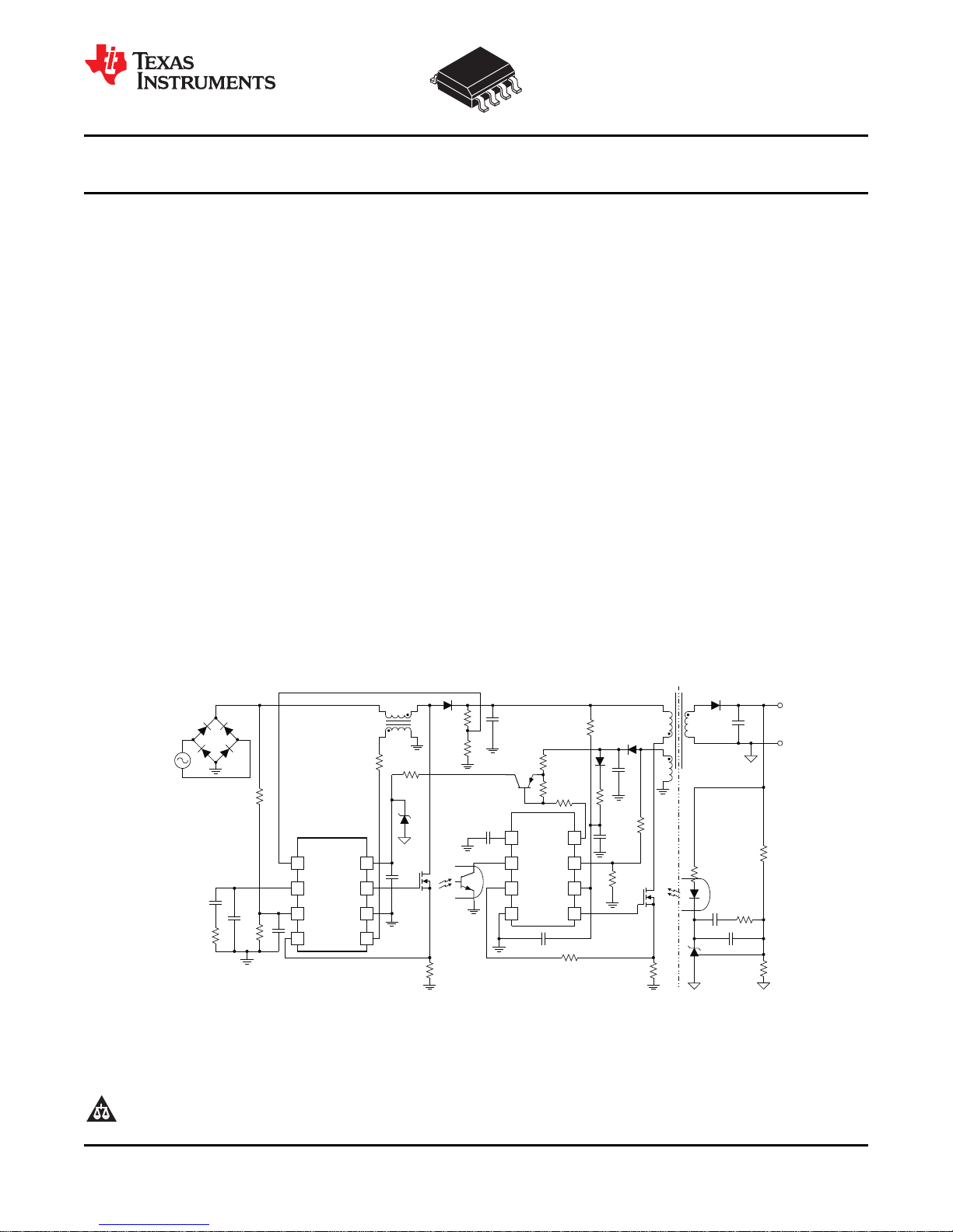
TYPICAL APPLICATION
1
2TrueDrive is a trademark of Texas Instruments.
PRODUCTION DATA information is current as of publication date.
Products conform to specifications per the terms of the Texas
Instruments standard warranty. Production processing does not
necessarily include testing of all parameters.
Please be aware that an important notice concerning availability, standard warranty, and use in critical applications of Texas
Instruments semiconductor products and disclaimers thereto appears at the end of this data sheet.
Copyright © 2005–2011, Texas Instruments Incorporated
Page 2
UCC28600
SLUS646J –NOVEMBER 2005– REVISED JULY 2011
www.ti.com
DESCRIPTION (CONT.)
The Design Calculator, (Texas Instruments Literature number SLVC104), located in the Tools and Software
section of the UCC28600 product folder, provides a user-interactive iterative process for selecting recommended
component values for an optimal design.
ABSOLUTE MAXIMUM RATINGS
over operating free-air temperature range unless otherwise noted
VDD Supply voltage range IDD< 20 mA 32 V
I
DD
I
OUT(sink)
I
OUT(source)
V
OVP
I
OVP(source)
V
STATUS
T
J
T
stg
T
LEAD
(1) Stresses beyond those listed under “absolute maximum ratings” may cause permanent damage to the device. These are stress ratings
only, and functional operation of the device at these or any other conditions beyond those indicated under “recommended operating
conditions” is not implied. Exposure to absolute-maximum-rated conditions for extended periods may affect device reliability. All voltages
are with respect to GND. Currents are positive into, negative out of the specified terminal. Consult Packaging Section of the databook
for thermal limitations and considerations of packages.
Supply current 20 mA
Output sink current (peak) 1.2
Output source current (peak) -0.8
Analog inputs FB, CS, SS -0.3 to 6.0
VDD = 0 V to 30 V 30 V
Power dissipation SOIC-8 package, TA= 25°C 650 mW
Operating junction temperature range –55 to 150
Storage temperature –65 to 150 °C
Lead temperature 1,6 mm (1/16 inch) from case for 10 seconds 300
(1)
UCC28600 UNIT
A
-1.0 to 6.0
-1.0 mA
V
RECOMMENDED OPERATING CONDITIONS
MIN NOM MAX UNIT
VDD Input voltage 21 V
I
T
Output sink current 0 A
OUT
Operating junction temperature -40 105 °C
J
ELECTROSTATIC DISCHARGE (ESD) PROTECTION
MIN MAX UNIT
Human body model 2000
CDM 1500
V
2 Copyright © 2005–2011, Texas Instruments Incorporated
Page 3
UCC28600
www.ti.com
SLUS646J –NOVEMBER 2005– REVISED JULY 2011
ELECTRICAL CHARACTERISTICS
VDD = 15 V, 0.1-μF capacitor from VDD to GND, 3.3-nF capacitor from SS to GND charged over 3.5 V, 500-Ω resistor from
OVP to -0.1 V, FB = 4.8 V, STATUS = not connected, 1-nF capacitor from OUT to GND, CS = GND, TA= -40°C to 105°C,
(unless otherwise noted)
PARAMETER TEST CONDITIONS MIN TYP MAX UNIT
Overall
I
STARTUP
I
STANDBY
I
DD
Undervoltage Lockout
VDD
(uvlo)
ΔVDD
(uvlo)
PWM (Ramp)
D
MIN
D
MAX
Oscillator (OSC)
f
QR(max)
f
QR(min)
f
SS
dTS/dFB VCO gain TSfor 1.6 V < VFB< 1.8 V -38 -30 -22 μs/V
Feedback (FB)
R
FB
V
FB
Status
R
DS(on)
I
STATUS(leakage)
(1) R
SCT
and C
Startup current VDD = V
-0.3 V 12 25
UVLO
Standby current VFB= 0 V 350 550
Operating current mA
Not switching 2.5 3.5
130 kHz, QR mode 5.0 7.0
VDD clamp FB = GND, IDD= 10 mA 21 26 32 V
Startup threshold 10.3 13.0 15.3
Stop threshold 6.3 8 9.3 V
Hysteresis 4.0 5.0 6.0
(1)
Minimum duty cycle VSS= GND, VFB= 2 V 0%
Maximum duty cycle QR mode, fS= max, (open loop) 99%
Maximum QR and DCM frequency 117 130 143
Minimum QR and FFM frequency VFB= 1.3 V 32 40 48 kHz
Soft start frequency VSS= 2.0 V 32 40 48
Feedback pullup resistor 12 20 28 kΩ
FB, no load QR mode 3.30 4.87 6.00
Green-mode ON threshold VFBthreshold 0.3 0.5 0.7
Green-mode OFF threshold VFBthreshold 1.2 1.4 1.6
Green-mode hysteresis VFBthreshold 0.7 0.9 1.1 V
FB threshold burst-ON VFBduring green mode 0.3 0.5 0.7
FB threshold burst-OFF VFBduring green mode 0.5 0.7 0.9
Burst Hysteresis VFBduring green mode 0.13 0.25 0.42
STATUS on resistance V
STATUS leakage/off current VFB= 0.44 V, V
are not connected in the circuit for maximum and minimum duty cycle tests, current sense tests and power limit tests.
CST
= 1 V 1.0 2.4 3.8 kΩ
STATUS
= 15 V -0.1 2.0 μA
STATUS
μA
Copyright © 2005–2011, Texas Instruments Incorporated 3
Page 4
UCC28600
SLUS646J –NOVEMBER 2005– REVISED JULY 2011
www.ti.com
ELECTRICAL CHARACTERISTICS (continued)
VDD = 15 V, 0.1-μF capacitor from VDD to GND, 3.3-nF capacitor from SS to GND charged over 3.5 V, 500-Ω resistor from
OVP to -0.1 V, FB = 4.8 V, STATUS = not connected, 1-nF capacitor from OUT to GND, CS = GND, TA= -40°C to 105°C,
(unless otherwise noted)
PARAMETER TEST CONDITIONS MIN TYP MAX UNIT
Current Sense (CS)
A
CS(FB)
V
CS(os)
Power Limit (PL)
I
PL(cs)
V
PL
Soft Start (SS)
I
SS(chg)
I
SS(dis)
V
SS
Overvoltage Protection (OVP)
I
OVP(line)
V
OVP(on)
V
OVP(load)
Thermal Protection (TSP)
OUT
t
RISE
t
FALL
(2) R
(3) Ensured by design. Not production tested.
SCT
and C
(2)
Gain, FB = ΔVFB/ ΔV
CS
QR mode 2.5 V/V
Shutdown threshold VFB= 2.4 V, VSS= 0 V 1.13 1.25 1.38 V
CS to output delay time (power limit) CS = 1.0 V
CS to output delay time (over current
fault)
CS = 1.45 V
PULSE
PULSE
100 175 300
50 100 150
CS discharge impedance CS = 0.1 V, VSS= 0 V 25 115 250 Ω
CS offset SS mode, VSS≤ 2.0 V, via FB 0.35 0.40 0.45 V
(2)
CS current OVP = -300 μA -165 -150 -135 μA
CS working range QR mode, peak CS voltage 0.70 0.81 0.92
PL threshold Peak CS voltage + CS offset 1.05 1.20 1.37
Softstart charge current VSS= GND -8.3 -6.0 -4.5 μA
Softstart discharge current VSS= 0.5 V 2.0 5.0 10 mA
Switching ON threshold Output switching start 0.8 1.0 1.2 V
Line overvoltage protection I
OVP voltage at OUT = HIGH -125 -25 mV
Load overvoltage protection V
Thermal shutdown (TSP) temperature
(3)
threshold, OUT = HI -512 -450 -370 μA
OVP
VFB= 4.8 V, VSS= 5.0 V, I
μA
threshold, OUT = LO 3.37 3.75 4.13 V
OVP
OVP(on)
, = -300
130 140 150
Thermal shutdown hysteresis 15
Rise time 10% to 90% of 13 V typical out clamp 50 75
Fall time 10 20
are not connected in the circuit for maximum and minimum duty cycle tests, current sense tests and power limit tests.
CST
ns
V
°C
ns
4 Copyright © 2005–2011, Texas Instruments Incorporated
Page 5
STATUS
GND
V
FB
V
CS
V
OVP
V
OUT
V
DD
I
DD
I
OVP
R
OVP
500 Ω
C
OUT
1.0 nF
R
OUT
10 Ω
C
BIAS
1 µF
CDD 100 nF
I
CS
C
FB
47 pF
C
SS
3.3 nF
C
CST
560 pF
See Note
R
CST
37.4 kΩ
See Note
SS
VDD
GND
OUT
FB
CS
OVP
STATUS
UCC28600
+
1
2
3
4 5
6
7
8
5 V
2
1
6
5.0
VREF
SS
VDD
4
GND
5
OUT
FB
1.5R
8
3
CS
UVLO
+
C
BULK
Feedback
20kW
C
SS
7
OVP
On-Chip
Thermal
Shutdown
REF
26V
R
STATUS
13/8V
R
CS
R
OVP1
R
OVP2
C
VDD
+
400mV
REF
R
SU
+
Q
Q
SET
CLR
D
REF
GAIN=1/2.5
+
Modulation
Comparison
UCC28600
FaultLogic
LINE_OVP
LOAD_OVP
REF_OK
RUN
UVLO
CS
OVR_T
STATUS
SS_DIS
GREENMODE
FB_CLAMP
OSC_CL
FB
QRDETECT
LOAD_OVP
LINE_OVP
QR_DONE
____
OUT
CS
OSCILLATOR
QR_DONE
CLK
RUN
SS_OVR
OSC_CL
R
PL
PL
1.2V
SS_OVR BURST BURST
R
VDD
VDD
UCC28600
www.ti.com
OPEN LOOP TEST CIRCUIT
R
and C
CST
sense tests and power limit tests.
are not connected for maximum and minimum duty cycle tests, current
CST
SLUS646J –NOVEMBER 2005– REVISED JULY 2011
NOTE
BLOCK DIAGRAM/TYPICAL APPLICATION
Copyright © 2005–2011, Texas Instruments Incorporated 5
Page 6
1
2
3
4
8
7
6
5
SS
FB
CS
GND
STATUS
OVP
VDD
OUT
UCC28600
D PACKAGE
(TOP VIEW)
UCC28600
SLUS646J –NOVEMBER 2005– REVISED JULY 2011
www.ti.com
ORDERING INFORMATION
T
A
-40°C to 105°C SOIC (D)
(1) SOIC (D) package is available taped and reeled by adding “R” to the above part numbers. Reeled quantities for UCC28600DR is 2,500
devices per reel.
PACKAGES PART NUMBER
(1)
UCC28600D
DEVICE INFORMATION
TERMINAL FUNCTIONS
TERMINAL
NAME NO.
CS 3 I protection. The CS voltage input originates across a current sense resistor and ground. Power limit is
FB 2 I Connect the collector of the photo-transistor of the feedback optocoupler directly to this pin; connect the emitter
GND 4 -
OUT 5 O
OVP 7 I Detect line, load and resonant conditions using the primary bias winding of the transformer, adjust sensitivity
SS 1 I be placed as close as possible to the SS pin and GND, keeping trace length to a minimum. All faults discharge
STATUS 8 O disable the PFC control circuit (high impedance = green mode). STATUS pin is high during UVLO, (VDD <
VDD 6 I pin, as described in the GND pin description. Operating energy is usually delivered from auxiliary winding. To
I/O DESCRIPTION
Current sense input. Also programs power limit, and used to control modulation and activate overcurrent
programmed with an effective series resistance between this pin and the current sense resistor.
Feedback input or control input from the optocoupler to the PWM comparator used to control the peak current
in the power MOSFET. An internal 20-kΩ resistor is between this pin and the internal 5-V regulated voltage.
of the photo-transistor to GND. The voltage of this pin controls the mode of operation in one of the three
modes: quasi resonant (QR), frequency foldback mode (FFM) and green mode (GM).
Ground for internal circuitry. Connect a ceramic 0.1-μF bypass capacitor between VDD and GND, with the
capacitor as close to these two pins as possible.
1-A sink (TrueDrive™ ) and 0.75-A source gate drive output. This output drives the power MOSFET and
switches between GND and the lower of VDD or the 13-V internal output clamp.
Over voltage protection (OVP) input senses line-OVP, load-OVP and the resonant trough for QR turn-on.
with resistors connected to this pin.
Soft-start programming pin. Program the soft-start rate with a capacitor to ground; the rate is determined by the
capacitance and the internal soft-start charge current. Placement of the soft-start capacitor is critical and should
the SS pin to GND through an internal MOSFET with an R
comparator reacts to the lowest of the SS voltage, the internal FB voltage and the peak current limit.
ACTIVE HIGH open drain signal that indicates the device has entered standby mode. This pin can be used to
startup threshold), and softstart, (SS < FB).
Provides power to the device. Use a ceramic 0.1-μF by-pass capacitor for high-frequency filtering of the VDD
prevent hiccup operation during start-up, a larger energy storage cap is also needed between VDD and GND.
of approximately 100 Ω. The internal modulator
DS(on)
6 Copyright © 2005–2011, Texas Instruments Incorporated
Page 7
R
CS
+
ǒ
VPL* V
CS(os)
Ǔǒ
I
CS(2)
* I
CS(1)
Ǔ
I
CS(2)IP(1)
* I
CS(1)IP(2)
R
PL
+
ǒ
VPL* V
CS(os)
Ǔǒ
I
P(2)
* I
P(1)
Ǔ
I
CS(1)IP(2)
* I
CS(2)IP(1)
R
OVP1
+
1
I
OVP(line)
ǒ
N
B
N
P
V
BULK(ov)
Ǔ
R
OVP2
+ R
OVP1
ȧ
ȧ
ȡ
Ȣ
V
OVP(load)
N
B
N
S
ǒ
V
OUT(shutdown)
) V
F
Ǔ
* V
OVP(load)
ȧ
ȧ
ȣ
Ȥ
UCC28600
www.ti.com
TERMINAL COMPONENTS
TERMINAL
NAME NO.
CS 3 I
FB 2 I Opto-isolator collector
GND 4 - Bypass capacitor to VDD, CBP= 0.1 μF
OUT 5 O Power MOSFET gate
I/O DESCRIPTION
where:
• IP1is the peak primary current at low line, full load
• IP2is the peak primary current at high line, full load
• I
CS1
• I
CS2
• VPLis the Power Limit (PL) threshold
• V
CS(os)
(1) (2) (3)
is the power limit current that is sourced at the CS pin at low-line voltage
is the power limit current that is sourced at the CS pin at high-line voltage
is the CS offset voltage
(2)
SLUS646J –NOVEMBER 2005– REVISED JULY 2011
(1)
(3)
(3)
(3)
(3)
(2)
OVP 7 I
(1) Refer to Figure 1 for all reference designators in the Terminal Components Table.
(2) Refer to the Electrical Characteristics Table for constant parameters.
(3) Refer to the UCC28600 Design Calculator (TI Literature Number SLVC104) or laboratory measurements for currents, voltages and times
in the operational circuit.
Copyright © 2005–2011, Texas Instruments Incorporated 7
where:
• I
OVP(line)
• V
BULK(ov)
• V
OVP(load)
• V
OUT(shutdown)
• VFis the forward voltage of the secondary rectifier
• NBis the number of turns on the bias winding
• NSis the number of turns on the secondary windings
• NPis the number of turns on the primary windings
is OVP
is the allowed input over- voltage level
is OVP
current threshold
line
(2)
load
is the allowed output over-voltage level
(2)
(3)
(3)
(3)
(3)
(3)
Page 8
CSSu I
SS
t
SS(min)
(
due power limit
)
A
CS(FB)
ǒ
VPL* V
CS(os)
Ǔ
t
SS(min)
+
ȧ
ȧ
ȱ
Ȳ
* R
LOAD(ss)COUT
2
ȏn
ȧ
ȡ
Ȣ
1 *
ǒ
V
OUT
* DV
OUT(step)
Ǔ
2
R
LOAD(ss)POUT(max)limit
ȧ
ȣ
Ȥ
ȧ
ȧ
ȳ
ȴ
t
SS(min)
+
ȧ
ȱ
Ȳ
C
OUTVOUT
2
2 P
LIM
ȧ
ȳ
ȴ
R
ST2
+
V
BE(off)
I
STATUS(leakage)
R
ST1
+
R
ST2
ƪ
VDD
(uvlo*on)
* V
BE(sat)
* R
DS(on)
ǒ
I
CC
b
sat
Ǔ
ƫ
* R
DS(on)VBE(sat)
ǒ
ǒ
I
CC
b
sat
Ǔ
R
ST2
Ǔ
) V
BE(sat)
UCC28600
SLUS646J –NOVEMBER 2005– REVISED JULY 2011
TERMINAL COMPONENTS (continued)
TERMINAL
NAME NO.
SS 1 I
I/O DESCRIPTION
where t
or
• R
LOAD(ss)
• ΔV
• P
OUT(max limit)
• A
CS(FB)
• V
CS(os)
• ISSis the soft-start charging current
• VPLis the power limit threshold
(1) (2) (3)
is the greater of:
SS(min)
is the effective load impedance during soft-start
OUT(step)
is the allowed change in V
is the current sense gain
is the CS offset voltage
due to a load step
Programmed power limit level, in W
OUT
(5)
(5)
(5)
(5)
www.ti.com
(2)
(4)
(4)
(4)
STATUS 8 O
where:
• β
• V
• VDD
• ICCis the collector current of Q
• I
• V
• R
(4) Refer to the UCC28600 Design Calculator (TI Literature Number SLVC104) or laboratory measurements for currents, voltages and times
in the operational circuit.
(5) Refer to the Electrical Characteristics Table for constant parameters.
8 Copyright © 2005–2011, Texas Instruments Incorporated
is the gain of transistor QSTin saturation
SAT
BE(sat)
(uvlo-on)
STATUS(leakage)
is the maximum allowable voltage across the base emitter junction that will not turn QSTon
BE(off)
DS(on)
is the base-emitter voltage of transistor QSTin saturation
is the startup threshold
is the maximum leakage/off current of the STATUS pin
is the R
DS(on)
of STATUS
(5)
ST
(5)
(5)
Page 9
C
VDD
+
ƪ
ǒ
IDD) C
ISSVOUT(hi)fQR(max)
Ǔ
T
BURST
DV
DD(burst)
ƫ
C
VDD
+
ƪ
ǒ
IDD) C
ISSVOUT(hi)fQR(max)
Ǔ
t
SS
DVDD
(uvlo)
ƫ
R
VDD
+
ǒ
p
4
Ǔ
ǒ
N
B
NP
Ǔ
ȧ
ȡ
Ȣ
ǒ
V
DS1(os)fQR(max)LLEAKAGE
ǒ
CD) C
SNUB
Ǔ
Ǹ
IDD) C
ISSVOUT(hi)fQR(max)
ȧ
ȣ
Ȥ
R
SU
+
V
BULK(min)
I
STARTUP
UCC28600
www.ti.com
TERMINAL COMPONENTS (continued)
TERMINAL
NAME NO.
VDD 6 I
(6) Refer to the Electrical Characteristics Table for constant parameters.
(7) Refer to the UCC28600 Design Calculator (TI Literature Number SLVC104) or laboratory measurements for currents, voltages and times
in the operational circuit.
I/O DESCRIPTION
C
is the greater of:
VDD
or
where:
• IDDis the operating current of the UCC28600
• C
ISS
• V
OUT(hi)
• f
QR(max)
• T
BURST
• ΔVDD
• ΔVDD
• V
DS1(os)
• L
LEAKAGE
• CDis the total drain node capacitance of MOSFET M
• I
STARTUP
• C
SNUB
• tSSis the soft start charge time
(1) (2) (3)
(6)
is the input capacitance of MOSFET M
is VOH of the OUT pin, either 13 V (typ) V
is fSat high line, maximum load
is the measured burst mode period
is the allowed VDDripple during burst mode
(burst)
is the UVLO hysteresis
(uvlo)
is the amount of drain-source overshoot voltage
is the leakage inductance of the primary winding
is IDDstart-up current of the UCC28600
is the snubber capacitor value
(6)
(7)
1
(6)
OUT
(6)
SLUS646J –NOVEMBER 2005– REVISED JULY 2011
(3)
clamp or less as measured
1
Copyright © 2005–2011, Texas Instruments Incorporated 9
Page 10
C
BULK
FEEDBACK
C
SS
R
CS
R
OVP1
R
OVP2
C
VDD
D1
R
SU
R
PL
TL431
2
1
6
SS
VDD
4 GND 5OUT
FB
8
3 CS
7OVP
STATUS
UCC28600
C
BP
100nF
R
ST2
R
ST1
C
OUT
PRIMARY SECONDARY
N
1
N
B
N
2
V
OUT
+
-
+
-
V
BULK
I
CC
R
VDD
Q
ST
R
OUT
R
SNUB
C
SNUB
M
1
PFC OUTPUT
or
BRIDGE RECTIFIER
PFC CONTROLLER BIAS
(if used)
C
BIAS
D2
UCC28600
SLUS646J –NOVEMBER 2005– REVISED JULY 2011
www.ti.com
Figure 1. Pin Termination Schematic
10 Copyright © 2005–2011, Texas Instruments Incorporated
Page 11

V
FB
0.5V0.7V 1.4V 2.0V 4.0V 5.0V
GreenMode-ON,
Burst-OFF
GreenMode-OFF,
Burst-ON
Burst
Hysteresis
0V
GreenMode
Hysteresis
GreenMode
FFM
40kHz < f
S
< 130kHz
V
FB
Control Range Limit
InternalReference
QR Mode or DCMMode
UCC28600
www.ti.com
SLUS646J –NOVEMBER 2005– REVISED JULY 2011
APPLICATION INFORMATION
Functional Description
The UCC28600 is a multi-mode controller, as illustrated in Figure 3 and Figure 4. The mode of operation
depends upon line and load conditions. Under all modes of operation, the UCC28600 terminates the OUT = HI
signal based on the switch current. Thus, the UCC28600 always operates in current mode control so that the
power MOSFET current is always limited.
Under normal operating conditions, the FB pin commands the operating mode of the UCC28600 at the voltage
thresholds shown in Figure 2. Soft-start and fault responses are the exception. Soft-start mode hard-switch
controls the converter at 40 kHz. The soft-start mode is latched-OFF when VFBbecomes less than VSSfor the
first time after UVLOON. The soft-start state cannot be recovered until after passing UVLO
At normal rated operating loads (from 100% to approximately 30% full rated power) the UCC28600 controls the
converter in quasi-resonant mode (QRM) or discontinuous conduction mode (DCM), where DCM operation is at
the clamped maximum switching frequency (130 kHz). For loads that are between approximately 30% and 10%
full rated power, the converter operates in frequency foldback mode (FFM), where the peak switch current is
constant and the output voltage is regulated by modulating the switching frequency for a given and fixed VIN.
Effectively, operation in FFM results in the application of constant volt-seconds to the flyback transformer each
switching cycle. Voltage regulation in FFM is achieved by varying the switching frequency in the range from 130
kHz to 40 kHz. For extremely light loads (below approximately 10% full rated power), the converter is controlled
using bursts of 40-kHz pulses. Keep in mind that the aforementioned boundaries of steady-state operation are
approximate because they are subject to converter design parameters.
Refer to the typical applications block diagram for the electrical connections to implement the features.
, and then, UVLOON.
OFF
Copyright © 2005–2011, Texas Instruments Incorporated 11
Figure 2. Mode Control with FB Pin Voltage
Page 12

START
VDD > 13V?
Soft Start
Monitor V
FB
VFB> 2.0V1.4V < VFB< 2.0VVFB< 1.4V
Fixed V /s
Freq. Foldback
(Light Load)
Quasi-Resonant
Mode or DCM
(Normal Load)
VFB< 0.5V
VDD < 8V?
REF < 4V?
OVP = Logic High?
OT = Logic High?
OC = Logic High
RUN = Logic High
STATUS = Hi Z
Y
N
Y
Y
RUN = Logic Low
STATUS = Hi Z
Fixed V-sec
40kHz Burst
N
N
Fixed V /s
40kHz
Zero Pulses
STATUS = Hi Z
(In Green-Mode)
VFB> 1.2V?VFB> 1.5V?
STATUS = 0V
(In Run-Mode)
STATUS = 0V
(In Run-Mode)
STATUS = 0V
(In Run-Mode)
N
N
YY
RUN = Logic Low
Continuous Fault
Monitor
UCC28600
SLUS646J –NOVEMBER 2005– REVISED JULY 2011
www.ti.com
Figure 3. Control Flow Chart
12 Copyright © 2005–2011, Texas Instruments Incorporated
Page 13

fsw
QR Mode
Switching
Frequency
Feedback
Voltage
Power Supply
Output Voltage
t
t
t
(40 kHz)
This mode applies bursts of
40kHz soft−start pulses to the
power MOSFET gate. The
average fsw is shown in this
operating mode.
DCM
(maximum fs)
IC Off
Softstart
Regular Operation
Green Mode
Peak MOSFET
Current
t
Fixed Frequency
Status, pulled up
to VDD
t
Green Mode,
PFC bias OFF
Load Power
t
f
MAX
=
Oscillator Frequency
(130 kHz)
SS Mode
(Fixed fSW )
f
SS
V
FB
V
OUT
V
STATUS
Load shown is slightly
less than overcurrent
threshold
P
OUT, (max)
P
OUT
f
GRMODE_MX
(40 kHz)
f
QR_MIN
Internally Limit-
ed to 40 kHz
Hysteretic
Transition into
Green Mode
Frequency
Foldback
(Valley Switching, VS)
(VS)
FFM, (VS)
Green Mode
Burst Hysteresis
UCC28600
www.ti.com
SLUS646J –NOVEMBER 2005– REVISED JULY 2011
Copyright © 2005–2011, Texas Instruments Incorporated 13
Figure 4. Operation Mode Switching Frequencies
Page 14

OSC_CL
QR_DONE
4.0V
0.1V
SS_OVR
REF
S Q
QR
CLK
130 kHz OSC
Clamp
Comparator
OSC Valley
Comparator
OSC Peak
Comparator
RUN
+
+
+
Oscillator
+
+
+
FB_CL
OSC_CL
FB
1.4 V
2.0 V
450 kΩ
450 kΩ
100 kΩ
100 kΩ
Mode Clamps
UCC28600
SLUS646J –NOVEMBER 2005– REVISED JULY 2011
www.ti.com
Details of the functional boxes in the Block Diagram/Typical Application drawing are shown in Figure 5, Figure 6,
Figure 7 and Figure 8. These figures conceptualize how the UCC28600 executes the command of the FB voltage
to have the responses that are shown in Figure 2, Figure 3 and Figure 4. The details of the functional boxes also
conceptualize the various fault detections and responses that are included in the UCC28600. During all modes of
operation, this controller operates in current mode control. This allows the UCC28600 to monitor the FB voltage
to determine and respond to the varying load levels such as heavy, light or ultra-light.
Quasi-resonant mode and DCM occurs for feedback voltages VFBbetween 2.0 V and 4.0 V, respectively. In turn,
the CS voltage is commanded to be between 0.4 V and 0.8 V. A cycle-by-cycle power limit imposes a fixed 0.8-V
limit on the CS voltage. An overcurrent shutdown threshold in the fault logic gives added protection against
high-current, slew-rate shorted winding faults, shown in Figure 8. The power limit feature in the QR DETECT
circuit of Figure 7 adds an offset to the CS signal that is proportional to the line voltage. The power limit feature is
programmed with RPL, as shown in the typical applications diagram.
14 Copyright © 2005–2011, Texas Instruments Incorporated
Figure 5. Oscillator Details
Figure 6. Mode Clamp Details
Page 15

R
SU
R
OVP2
C
IN
C
VDD
R
OVP1
Auxiliary
Winding
+
+
+
+
7
Slope
+
0.1 V
0.1 V
-0.1 V
REF (5 V)
1 kW
3.75 V
0.45 V
QR_DONE
(Oscillator)
LOAD_OVP
(Fault Logic)
LINE_OVP
(Fault Logic)
REF (5 V)
3CS
OVP
VDD
OUT (From Driver)
UCC28600
R
PL1
CS
R
CS
Power Limit
Offset
I
LINE
Burst
(from FAULT logic)
01
+
QR Detect
I
LINE
I
LINE
2
C
OUT
R
PL2
N
S
N
P
N
B
UCC28600
www.ti.com
SLUS646J –NOVEMBER 2005– REVISED JULY 2011
Figure 7. QR Detect Details
Copyright © 2005–2011, Texas Instruments Incorporated 15
Page 16

S Q
QR
REF
D Q
Q
CLR
SET
Power−Up Reset
Thermal
Shutdown
+
+
1.25 V
+
SS/DIS
RUN
3 CS
OVR_T
LINE_OVP
(QR Detect)
LOAD_OVP
(QR Detect)
UVLO
REF_OK
Burst
REF
(5 V)
FB
7
FB
CS
SS_OVR
STATUS8
UCC28600
BURST
Over−Current
Shutdown
20 kΩ
Fault Logic
0.5 V/0.7 V
0.5 V/1.4 V
UCC28600
SLUS646J –NOVEMBER 2005– REVISED JULY 2011
www.ti.com
Figure 8. Fault Logic Details
Quasi-Resonant / DCM Control
Quasi-resonant (QR) and DCM operation occur for feedback voltages VFBbetween 2.0 V and 4.0 V. In turn, the
peak CS voltage is commanded to be between 0.4 V and 0.8 V. During this control mode, the rising edge of OUT
always occurs at the valley of the resonant ring after demagnetization. Resonant valley switching is an integral
part of QR operation. Resonant valley switching is also imposed if the system operates at the maximum
switching frequency clamp. In other words, the frequency varies in DCM operation in order to have the switching
event occur on the first resonant valley that occurs after a 7.7-μs (130-kHz) interval. Notice that the CS pin has
an internal dependent current source, 1/2 I
. This current source is part of the cycle-by-cycle power limit
LINE
function that is discussed in the Protection Features section.
Frequency Foldback Mode Control
Frequency foldback mode uses elements of the FAULT LOGIC, shown in Figure 8 and the mode clamp circuit,
shown in Figure 6. At the minimum operating frequency, the internal oscillator sawtooth waveform has a peak of
4.0 V and a valley of 0.1 V. When the FB voltage is between 2.0 V and 1.4 V, the FB_CL signal in Figure 6
commands the oscillator in a voltage controlled oscillator (VCO) mode by clamping the peak oscillator voltage.
The additional clamps in the OSCILLATOR restrict VCO operation between 40 kHz and 130 kHz. The FB_CL
voltage is reflected to the modulator comparator effectively clamping the reflected CS command to 0.4 V.
Green-Mode Control
Green mode uses element of the fault logic, shown in Figure 8 and the mode clamps circuit, shown in Figure 6.
The OSC_CL signal clamps the Green-mode operating frequency at 40 kHz. Thus, when the FB voltage is
between 1.4 V and 0.5 V, the controller is commanding an excess of energy to be transferred to the load which
in turn, drives the error higher and FB lower. When FB reaches 0.5 V, OUT pulses are terminated and do not
resume until FB reaches 0.7 V. In this mode, the converter operates in hysteretic control with the OUT pulse
terminated at a fixed CS voltage level of 0.4 V. The power limit offset is turned OFF during Green mode and it
returns to ON when FB is above 1.4 V, as depicted in Figure 8. Green mode reduces the average switching
frequency in order to minimize switching losses and increase the efficiency at light load conditions.
16 Copyright © 2005–2011, Texas Instruments Incorporated
Page 17

8
5
VCC
GND
UCC28051
C
VCC
0.1 mF
C
BULK
2
4
8
6
STATUS
VDD
FB
GND
UCC28600
R
ST1
R
ST2
R
CS
C
VDD
Primary Secondary
10 V
TL431
Feedback
M1
Q1
To Zero
Current
Detection
M2
R
VCC
C
BIAS
R
SU
N
B
N
P
N
S
D
Z1
D
BIAS
D
VDD
UCC28600
www.ti.com
SLUS646J –NOVEMBER 2005– REVISED JULY 2011
Fault Logic
Advanced logic control coordinates the fault detections to provide proper power supply recovery. This provides
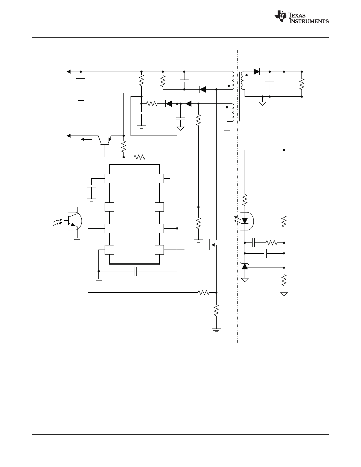
the conditioning for the thermal protection. Line overvoltage protection (line OVP) and load OVP are
implemented in this block. It prevents operation when the internal reference is below 4.5 V. If a fault is detected
in the thermal shutdown, line OVP, load OVP, or REF, the UCC28600 undergoes a shutdown/retry cycle.
Refer to the fault logic diagram in Figure 8 and the QR detect diagram in Figure 7 to program line OVP and load
OVP. To program the load OVP, select the R
shut-down voltage. To program line OVP, select the impedance of the R
μA when the V
is 0.45 V during the ON-time of the power MOSFET at the highest allowable input voltage.
OVP
OVP1
– R
divider ratio to be 3.75 V at the desired output
OVP2
OVP1
– R
combination to draw 450
OVP2
Oscillator
The oscillator, shown in Figure 5, is internally set and trimmed so it is clamped by the circuit in Figure 5 to a
nominal 130-kHz maximum operating frequency. It also has a minimum frequency clamp of 40 kHz. If the FB
voltage tries to drive operation to less than 40 kHz, the converter operates in green mode.
Status
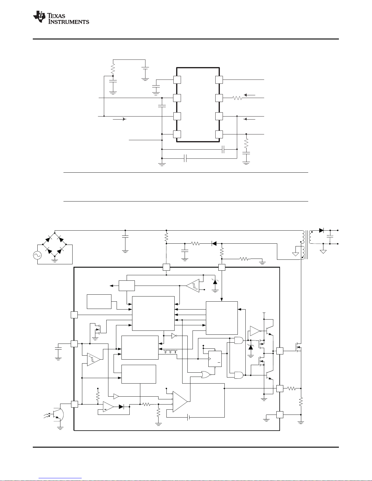
The STATUS pin is an open drain output, as shown in Figure 8. The status output goes into the OFF-state when
FB falls below 0.5 V and it returns to the ON-state (low impedance to GND) when FB rises above 1.4 V. This pin
is used to control bias power for a PFC stage, as shown in Figure 9. Key elements for implementing this function
include QST, R
ST1
and R
, as shown in the figure. Resistors R
ST2
ST1
and R
are selected to saturate QSTwhen it
ST2
is desirable for the PFC to be operational. During green mode, the STATUS pin becomes a high impedance and
R
causes QSTto turn-OFF, thus saving bias power. If necessary, use a zener diode and a resistor (DZ1and
ST1
RCC) to maintain VCCin the safe operating range of the PFC controller. Note the D
addition to the standard D
BIAS
- C
components. This added stage is required to isolate the STATUS circuitry
BIAS
VDD
- C
combination is in
VDD
from the startup resistor, RSU, to ensure there is no conduction through STATUS when VDD is below the UVLO
turn-on threshold.
Copyright © 2005–2011, Texas Instruments Incorporated 17
Figure 9. Using STATUS for PFC Shut-Down During Green Mode
Page 18

UCC28600
SLUS646J –NOVEMBER 2005– REVISED JULY 2011
www.ti.com
Operating Mode Programming
Boundaries of the operating modes are programmed by the flyback transformer and the four components RPL,
RCS, R
OVP1
and R
; shown in the Block Diagram/Application drawing.
OVP2
The transformer characteristics that predominantly affect the modes are the magnetizing inductance of the
primary and the magnitude of the output voltage, reflected to the primary. To a lesser degree (yet significant), the
boundaries are affected by the MOSFET output capacitance and transformer leakage inductance. The design
procedure here is to select a magnetizing inductance and a reflected output voltage that operates at the
DCM/CCM boundary at maximum load and maximum line. The actual inductance should be noticeably smaller to
account for the ring between the magnetizing inductance and the total stray capacitance measured at the drain
of the power MOSFET. This programs the QR/DCM boundary of operation. All other mode boundaries are preset
with the thresholds in the oscillator and green-mode blocks.
The four components RPL, RCS, R
OVP1
and R
must be programmed as a set due to the interactions of the
OVP2
functions. The use of the UCC28600 design calculator, TI Literature Number SLVC104, is highly recommended
in order to achieve the desired results with a careful balance between the transformer parameters and the
programming resistors.
Protection Features
The UCC28600 has many protection features that are found only on larger, full featured controllers. Refer to the
Block Diagram/Typical Application and Figures 1, 4, 5, 6 and 7 for detailed block descriptions that show how the
features are integrated into the normal control functions.
Overtemperature
Overtemperature lockout typically occurs when the substrate temperature reaches 140°C. Retry is allowed if the
substrate temperature reduces by the hysteresis value. Upon an overtemperature fault, CSSon softstart is
discharged and STATUS is forced to a high impedance.
18 Copyright © 2005–2011, Texas Instruments Incorporated
Page 19

UCC28600
www.ti.com
SLUS646J –NOVEMBER 2005– REVISED JULY 2011
Cycle-by-Cycle Power Limit
The cycle terminates when the CS voltage plus the power limit offset exceeds 1.2 V.
In order to have power limited over the full line voltage range of the QR Flyback converter, the CS pin voltage
must have a component that is proportional to the primary current plus a component that is proportional to the
line voltage due to predictable switching frequency variations due to line voltage. At power limit, the CS pin
voltage plus the internal CS offset is compared against a constant 1.2-V reference in the PWM comparator. Thus
during cycle-by-cycle power limit, the peak CS voltage is typically 0.8 V.
The current that is sourced from the OVP pin (I
) is reflected to a dependent current source of ½ I
LINE
LINE
, that is
connected to the CS pin. The power limit function can be programmed by a resistor, RPL, that is between the CS
pin and the current sense resistor. The current, I
NB/NPand resistor R
OVP1
. Current I
is programmed to set the line over voltage protection. Resistor RPLresults
LINE
, is proportional to line voltage by the transformer turns ratio
LINE
in the addition of a voltage to the current sense signal that is proportional to the line voltage. The proper amount
of additional voltage has the effect of limiting the power on a cycle-by-cycle basis. Note that RCS, RPL, R
R
must be adjusted as a set due to the functional interactions.
OVP2
OVP1
and
Current Limit
When the primary current exceeds maximum current level which is indicated by a voltage of 1.25 V at the CS
pin, the device initiates a shutdown. Retry occurs after a UVLO
/UVLOONcycle.
OFF
Over-Voltage Protection
Line and load over voltage protection is programmed with the transformer turn ratios, R
OVP1
and R
. The OVP
OVP2
pin has a 0-V voltage source that can only source current; OVP cannot sink current.
Line over voltage protection occurs when the OVP pin is clamped at 0 V. When the bias winding is negative,
during OUT = HI or portions of the resonant ring, the 0-V voltage source clamps OVP to 0 V and the current that
is sourced from the OVP pin is mirrored to the Line_OVP comparator and the QR detection circuit. The
Line_OVP comparator initiates a shutdown-retry sequence if OVP sources any more than 450 μA.
Load-over voltage protection occurs when the OVP pin voltage is positive. When the bias winding is positive,
during demagnetization or portions of the resonant ring, the OVP pin voltage is positive. If the OVP voltage is
greater than 3.75 V, the device initiates a shutdown. Retry occurs after a UVLO
/UVLOONcycle.
OFF
Undervoltage Lockout
Protection is provided to guard against operation during unfavorable bias conditions. Undervoltage lockout
(UVLO) always monitors VDD to prevent operation below the UVLO threshold.
Copyright © 2005–2011, Texas Instruments Incorporated 19
Page 20

–50 0 100 150
T – Temperature – °C
J
21
23
25
27
50
29
31
VDD – Clamp Voltage – V
–50 0 100 150
T – Temperature – °C
J
117
122
127
132
50
137
142
f – Switching Frequency – kHz
S
–50 0 100 150
T – Temperature – °C
J
0.70
0.75
0.80
0.85
50
0.90
0.95
PL Threshold, QR Mode, Peak CS Voltage – V
–50 0 100 150
T – Temperature – °C
J
–512
–492
–472
–452
50
–432
–412
–392
–372
I – Over Voltage Protection Threshold – µA
OVP
UCC28600
SLUS646J –NOVEMBER 2005– REVISED JULY 2011
CLAMP VOLTAGE SWITCHING FREQUENCY
vs vs
TEMPERATURE TEMPERATURE
www.ti.com
TYPICAL CHARACTERISTICS
Figure 10. Figure 11.
PL THRESHOLD OVER VOLTAGE PROTECTION THRESHOLD
vs vs
TEMPERATURE TEMPERATURE
Figure 12. Figure 13.
20 Copyright © 2005–2011, Texas Instruments Incorporated
Page 21

R
PL1
+ R
PL
ǒ
R
CS
R
DCS
Ǔ
R
PL2
+
R
PL1
ǒ
R
CS
R
DCS
Ǔ
* 1
R
CS
R
PL1
R
PL2
From power
MOSFET
To CS
R
DCS
R
PL
From power
MOSFET
To CS
(a) (b)
UCC28600
www.ti.com
SLUS646J –NOVEMBER 2005– REVISED JULY 2011
PRACTICAL DESIGN NOTES
Non-Ideal Current Sense Value
Resistors RCS, RPL, R
converter. Often, the ideal value for RCSis not available because the selection range of current sense resistors is
too coarse to meet the required power limit tolerances. This issue can be solved by using the next larger
available value of RCSand use a resistive divider with a Thevenin resistance that is equal to the ideal RPLvalue
in order to attenuate the CS signal to its ideal value, as shown in Figure 14. The equations for modifying the
circuit are:
• R
= ideal, but non-standard, value of current sense resistor.
DCS
• RPL= previously calculated value of the power limit resistor.
• RCS= available, standard value current sense resistor.
The board should be laid out to include R
readily available components.
OVP1
and R
must be programmed as a set due to functional interactions in the
OVP2
in order to fascillitate final optimization of the design based upon
PL2
(4)
(5)
Figure 14. Modifications to Fit a Standard Current Sense Resistor Value
Copyright © 2005–2011, Texas Instruments Incorporated 21
Page 22

PRIMARY SECONDARY
+
−
+
−
+
−
PRIMARY SECONDARY
+
−
+
−
+
−
(a)
(c)
0V
0V
(b)
0V
0V
(d)
V
D
V
D
V
D
V
D
V
G
V
G
V
G
V
G
L
M
L
M
L
LEAK
L
LEAK
V
BULK
V
BULK
C
BULK
C
BULK
V
IN
V
IN
V
R
V
R
∆V
SNUB
∆V
SNUB
C
SNUB
C
SNUB
R
SNUB2
R
SNUB1
R
SNUB1
C
D
C
D
R
CS
R
CS
M
1
M
1
D
S
D
S
Reduced L
LEAK CD
Resonance
L
LEAK CD
Resonance
UCC28600
SLUS646J –NOVEMBER 2005– REVISED JULY 2011
www.ti.com
Snubber Damping
Resonance between the leakage inductance and the MOSFET drain capacitance can cause false load-OVP
faults, in spite of the typical 2-μs delay in load-OVP detection. The bias winding is sensitive to the overshoot and
ringing because it is well coupled to the primary winding. A technique to eliminate the problem is to use an R2CD
snubber instead of an RCD snubber, shown in Figure 15. A damping resistor added to the RCD snubber reduces
ringing between the drain capacitor and the inductance when the snubber diode commutates OFF.
Figure 15. (a) RCD Snubber, (b) RCD Snubber Waveform, (c) R2CD Snubber, (d) R2CD Snubber
Waveform
22 Copyright © 2005–2011, Texas Instruments Incorporated
Page 23

Pick
DV
SNUB
V
R
+ between 0.5 and 1
C
SNUB
+
I
cs(peak)
2
L
LEAK
ǒ
VR) DV
SNUB
Ǔ
2
* V
R
2
R
SNUB1
+ ǒ
1
2
)
V
R
DV
SNUB
Ǔ
1
C
SNUB
ǒ
1
f
S(max)
*
L
LEAKICS(peak)
DV
SNUB
Ǔ
( )
2
2
SNUB
R
R
SNUB
SNUB1
SNUB1
V
1 1
V 1
V
1
2 3
V 2
P R
R
é ù
é ù
ê ú
ê ú
D
æ ö
æ ö
ê ú
ê ú
+ ´ + ´
ç ÷
ç ÷
ê ú
è ø
ê ú
è ø
+
ê ú
ê ú
ë û
ë û
=
R
SNUB2
+
DV
SNUB
I
CS(peak)
PǒR
SNUB
Ǔ
+ I
CS(peak)
2
R
SNUB2
ȧ
ȧ
ȧ
ȧ
ȡ
Ȣ
1
3
L
LEAKfS(max)
ǒ
V
R
)
DV
SNUB
2
Ǔ
ȧ
ȧ
ȧ
ȧ
ȣ
Ȥ
Q +
2V
R
DV
SNUB
) 1
Ǹ
UCC28600
www.ti.com
Begin the design of the R2CD using the same procedure as designing an RCD snubber. Then, add the damping
resistor, R
Select a capacitor for ΔV
Pick R
SNUB
Pick R
SNUB2
. The procedure is as follows:
SNUB2
:
SNUB
to discharge C
to dampen the L
:
SNUB
LEAK-CSNUB
resonance with a Q that is between 1.7 and 2.2:
SLUS646J –NOVEMBER 2005– REVISED JULY 2011
(6)
(7)
(8)
(9)
For the original selection of ΔV
SNUB
(10)
(11)
,
(12)
Copyright © 2005–2011, Texas Instruments Incorporated 23
Page 24

UCC28600
SLUS646J –NOVEMBER 2005– REVISED JULY 2011
www.ti.com
REFERENCES
1. Power Supply Seminar SEM-1400 Topic 2: Design And Application Guide For High Speed MOSFET Gate
Drive Circuits, by Laszlo Balogh, Texas Instruments Literature Number SLUP133
2. Datasheet, UCC3581 Micro Power PWM Controller, Texas Instruments Literature Number SLUS295
3. Datasheet, UCC28051 Transition Mode PFC Controller, Texas Instruments Literature Number SLUS515
4. UCC28600 Design Calculator, A QR Flyback Designer.xls, spreadsheet for Microsoft Excel 2003, Texas
Instruments Literature Number SLVC104
5. Design Considerations for the UCC28600, Texas Instruments Literature Number SLUA399
RELATED PRODUCTS
• UCC28051 Transition Mode PFC Controller (SLUS515)
• UCC3581 Micro Power PWM Controller (SLUS295)
REVISION HISTORY
Changes from Revision H (November 2005) to Revision I Page
• Changed Equation 9 ........................................................................................................................................................... 23
24 Copyright © 2005–2011, Texas Instruments Incorporated
Page 25

PACKAGE OPTION ADDENDUM
www.ti.com
11-Apr-2013
Addendum-Page 1
PACKAGING INFORMATION
Orderable Device Status
(1)
Package Type Package
Drawing
Pins Package
Qty
Eco Plan
(2)
Lead/Ball Finish MSL Peak Temp
(3)
Op Temp (°C) Top-Side Markings
(4)
Samples
UCC28600D ACTIVE SOIC D 8 75 Green (RoHS
& no Sb/Br)
CU NIPDAU Level-1-260C-UNLIM -40 to 105 28600D
UCC28600DG4 ACTIVE SOIC D 8 75 Green (RoHS
& no Sb/Br)
CU NIPDAU Level-1-260C-UNLIM -40 to 105 28600D
UCC28600DR ACTIVE SOIC D 8 2500 Green (RoHS
& no Sb/Br)
CU NIPDAU Level-1-260C-UNLIM -40 to 105 28600D
UCC28600DRG4 ACTIVE SOIC D 8 2500 Green (RoHS
& no Sb/Br)
CU NIPDAU Level-1-260C-UNLIM -40 to 105 28600D
(1)
The marketing status values are defined as follows:
ACTIVE: Product device recommended for new designs.
LIFEBUY: TI has announced that the device will be discontinued, and a lifetime-buy period is in effect.
NRND: Not recommended for new designs. Device is in production to support existing customers, but TI does not recommend using this part in a new design.
PREVIEW: Device has been announced but is not in production. Samples may or may not be available.
OBSOLETE: TI has discontinued the production of the device.
(2)
Eco Plan - The planned eco-friendly classification: Pb-Free (RoHS), Pb-Free (RoHS Exempt), or Green (RoHS & no Sb/Br) - please check http://www.ti.com/productcontent for the latest availability
information and additional product content details.
TBD: The Pb-Free/Green conversion plan has not been defined.
Pb-Free (RoHS): TI's terms "Lead-Free" or "Pb-Free" mean semiconductor products that are compatible with the current RoHS requirements for all 6 substances, including the requirement that
lead not exceed 0.1% by weight in homogeneous materials. Where designed to be soldered at high temperatures, TI Pb-Free products are suitable for use in specified lead-free processes.
Pb-Free (RoHS Exempt): This component has a RoHS exemption for either 1) lead-based flip-chip solder bumps used between the die and package, or 2) lead-based die adhesive used between
the die and leadframe. The component is otherwise considered Pb-Free (RoHS compatible) as defined above.
Green (RoHS & no Sb/Br): TI defines "Green" to mean Pb-Free (RoHS compatible), and free of Bromine (Br) and Antimony (Sb) based flame retardants (Br or Sb do not exceed 0.1% by weight
in homogeneous material)
(3)
MSL, Peak Temp. -- The Moisture Sensitivity Level rating according to the JEDEC industry standard classifications, and peak solder temperature.
(4)
Multiple Top-Side Markings will be inside parentheses. Only one Top-Side Marking contained in parentheses and separated by a "~" will appear on a device. If a line is indented then it is a
continuation of the previous line and the two combined represent the entire Top-Side Marking for that device.
Important Information and Disclaimer:The information provided on this page represents TI's knowledge and belief as of the date that it is provided. TI bases its knowledge and belief on information
provided by third parties, and makes no representation or warranty as to the accuracy of such information. Efforts are underway to better integrate information from third parties. TI has taken and
continues to take reasonable steps to provide representative and accurate information but may not have conducted destructive testing or chemical analysis on incoming materials and chemicals.
TI and TI suppliers consider certain information to be proprietary, and thus CAS numbers and other limited information may not be available for release.
In no event shall TI's liability arising out of such information exceed the total purchase price of the TI part(s) at issue in this document sold by TI to Customer on an annual basis.
Page 26

PACKAGE OPTION ADDENDUM
www.ti.com
11-Apr-2013
Addendum-Page 2
OTHER QUALIFIED VERSIONS OF UCC28600 :
•
Automotive: UCC28600-Q1
NOTE: Qualified Version Definitions:
•
Automotive - Q100 devices qualified for high-reliability automotive applications targeting zero defects
Page 27

PACKAGE MATERIALS INFORMATION
www.ti.com 10-Apr-2015
TAPE AND REEL INFORMATION
*All dimensions are nominal
Device Package
Type
UCC28600DR SOIC D 8 2500 330.0 12.4 6.4 5.2 2.1 8.0 12.0 Q1
Package
Drawing
Pins SPQ Reel
Diameter
(mm)
Reel
Width
W1 (mm)
A0
(mm)B0(mm)K0(mm)P1(mm)W(mm)
Pin1
Quadrant
Pack Materials-Page 1
Page 28

PACKAGE MATERIALS INFORMATION
www.ti.com 10-Apr-2015
*All dimensions are nominal
Device Package Type Package Drawing Pins SPQ Length (mm) Width (mm) Height (mm)
UCC28600DR SOIC D 8 2500 340.5 338.1 20.6
Pack Materials-Page 2
Page 29

Page 30

Page 31

IMPORTANT NOTICE
Texas Instruments Incorporated and its subsidiaries (TI) reserve the right to make corrections, enhancements, improvements and other
changes to its semiconductor products and services per JESD46, latest issue, and to discontinue any product or service per JESD48, latest
issue. Buyers should obtain the latest relevant information before placing orders and should verify that such information is current and
complete. All semiconductor products (also referred to herein as “components”) are sold subject to TI’s terms and conditions of sale
supplied at the time of order acknowledgment.
TI warrants performance of its components to the specifications applicable at the time of sale, in accordance with the warranty in TI’s terms
and conditions of sale of semiconductor products. Testing and other quality control techniques are used to the extent TI deems necessary
to support this warranty. Except where mandated by applicable law, testing of all parameters of each component is not necessarily
performed.
TI assumes no liability for applications assistance or the design of Buyers’ products. Buyers are responsible for their products and
applications using TI components. To minimize the risks associated with Buyers’ products and applications, Buyers should provide
adequate design and operating safeguards.
TI does not warrant or represent that any license, either express or implied, is granted under any patent right, copyright, mask work right, or
other intellectual property right relating to any combination, machine, or process in which TI components or services are used. Information
published by TI regarding third-party products or services does not constitute a license to use such products or services or a warranty or
endorsement thereof. Use of such information may require a license from a third party under the patents or other intellectual property of the
third party, or a license from TI under the patents or other intellectual property of TI.
Reproduction of significant portions of TI information in TI data books or data sheets is permissible only if reproduction is without alteration
and is accompanied by all associated warranties, conditions, limitations, and notices. TI is not responsible or liable for such altered
documentation. Information of third parties may be subject to additional restrictions.
Resale of TI components or services with statements different from or beyond the parameters stated by TI for that component or service
voids all express and any implied warranties for the associated TI component or service and is an unfair and deceptive business practice.
TI is not responsible or liable for any such statements.
Buyer acknowledges and agrees that it is solely responsible for compliance with all legal, regulatory and safety-related requirements
concerning its products, and any use of TI components in its applications, notwithstanding any applications-related information or support
that may be provided by TI. Buyer represents and agrees that it has all the necessary expertise to create and implement safeguards which
anticipate dangerous consequences of failures, monitor failures and their consequences, lessen the likelihood of failures that might cause
harm and take appropriate remedial actions. Buyer will fully indemnify TI and its representatives against any damages arising out of the use
of any TI components in safety-critical applications.
In some cases, TI components may be promoted specifically to facilitate safety-related applications. With such components, TI’s goal is to
help enable customers to design and create their own end-product solutions that meet applicable functional safety standards and
requirements. Nonetheless, such components are subject to these terms.
No TI components are authorized for use in FDA Class III (or similar life-critical medical equipment) unless authorized officers of the parties
have executed a special agreement specifically governing such use.
Only those TI components which TI has specifically designated as military grade or “enhanced plastic” are designed and intended for use in
military/aerospace applications or environments. Buyer acknowledges and agrees that any military or aerospace use of TI components
which have not been so designated is solely at the Buyer's risk, and that Buyer is solely responsible for compliance with all legal and
regulatory requirements in connection with such use.
TI has specifically designated certain components as meeting ISO/TS16949 requirements, mainly for automotive use. In any case of use of
non-designated products, TI will not be responsible for any failure to meet ISO/TS16949.
Products Applications
Audio www.ti.com/audio Automotive and Transportation www.ti.com/automotive
Amplifiers amplifier.ti.com Communications and Telecom www.ti.com/communications
Data Converters dataconverter.ti.com Computers and Peripherals www.ti.com/computers
DLP® Products www.dlp.com Consumer Electronics www.ti.com/consumer-apps
DSP dsp.ti.com Energy and Lighting www.ti.com/energy
Clocks and Timers www.ti.com/clocks Industrial www.ti.com/industrial
Interface interface.ti.com Medical www.ti.com/medical
Logic logic.ti.com Security www.ti.com/security
Power Mgmt power.ti.com Space, Avionics and Defense www.ti.com/space-avionics-defense
Microcontrollers microcontroller.ti.com Video and Imaging www.ti.com/video
RFID www.ti-rfid.com
OMAP Applications Processors www.ti.com/omap TI E2E Community e2e.ti.com
Wireless Connectivity www.ti.com/wirelessconnectivity
Mailing Address: Texas Instruments, Post Office Box 655303, Dallas, Texas 75265
Copyright © 2015, Texas Instruments Incorporated
 Loading...