
1
FEATURES
DESCRIPTION
APPLICATIONS
UCC28230
UCC28231
www.ti.com
................................................................................................................................................... SLUS814A – FEBRUARY 2008 – REVISED JUNE 2008
Advanced PWM Controller for Bus Converters
• Programmable, Load Depended Off Time
Control
The UCC28230, UCC28231 PWM bus controllers are
optimized for use in high efficiency, high power
• Frequency Controlled Start Up Allows Small
density, unregulated intermediate bus converters.
Output Inductor, Low Ripple and Constant
Topologies include push-pull, half-bridge and
Current Start with Large Output Capacitor
full-bridge. External drivers, such as the UCC27200
• Two 0.2-A Push-Pull Outputs Provide Matched
120-V high-side/low-side drivers, can be used with
Control Signals D to External Drivers
this controller.
• Two Additional 1- D Outputs for Optimal Use
Low cost, small size and highly efficient solutions are
of Self-Driven or Control Driven Synchronous
provided by innovations such as:
Rectifiers
• Start-up frequency control circuit allowing small
• Unregulated, Fixed Volt-Second or Fixed
output inductor and the ability to start with large
Frequency Modes set by User
intermediate bus capacitor.
• Two, 1.5% Overall Accuracy Reference Voltage
• Load depended off-time control set by user.
Options: 5-V for UCC28230 and 3.3-V for
Additional 1-D control outputs can be used for
UCC28231
primary winding clamping in self-driven output
• Resistor Programmable Switching Frequency
synchronous rectifier applications or as drive signals
up to 1 MHz
for the control-driven synchronous rectifier.
• Cycle-by-Cycle Current Limit Allows Parallel
Cycle-by-cycle current limit prevents overstresses of
Operation with Droop Based Current Sharing
converter. If the over current condition causes less
than 80% duty cycle at the output, then after a
• Single External Capacitor sets Soft-Start and
programmed time the controller proceeds into
Over Current Hiccup Mode Parameters with
periodical shutdown and restart hiccup mode.
Restart
The UCC28230 provides 5 V, and the UCC28231
• Severe Short Circuit Hiccup with Restart or
provides 3.3-V precision reference voltages with 1.5%
Latch Off Protection Option by External
overall accuracy and 10-mA output current. This
Resistor
reference voltage can be used to supply
• Input Under Voltage Lock Out
housekeeping circuit and/or microcontroller. The
• Thermal Shutdown
precision reference voltage can also be used for
accurate setting of system parameters.
• Thermally Enhanced 3 mm × 2 mm SON-12
and TSSOP-14 Package Options
Other features include under-voltage lockout, thermal
shut down, programmable soft start, over-current
hiccup mode and short circuit protection with internal
restart by default that can be set into latch-off mode
• Intermediate Bus Isolated Converters
by an external resistor.
• DC-to-DC Transformers
1
Please be aware that an important notice concerning availability, standard warranty, and use in critical applications of Texas
Instruments semiconductor products and disclaimers thereto appears at the end of this data sheet.
PRODUCTION DATA information is current as of publication date.
Copyright © 2008, Texas Instruments Incorporated
Products conform to specifications per the terms of the Texas
Instruments standard warranty. Production processing does not
necessarily include testing of all parameters.
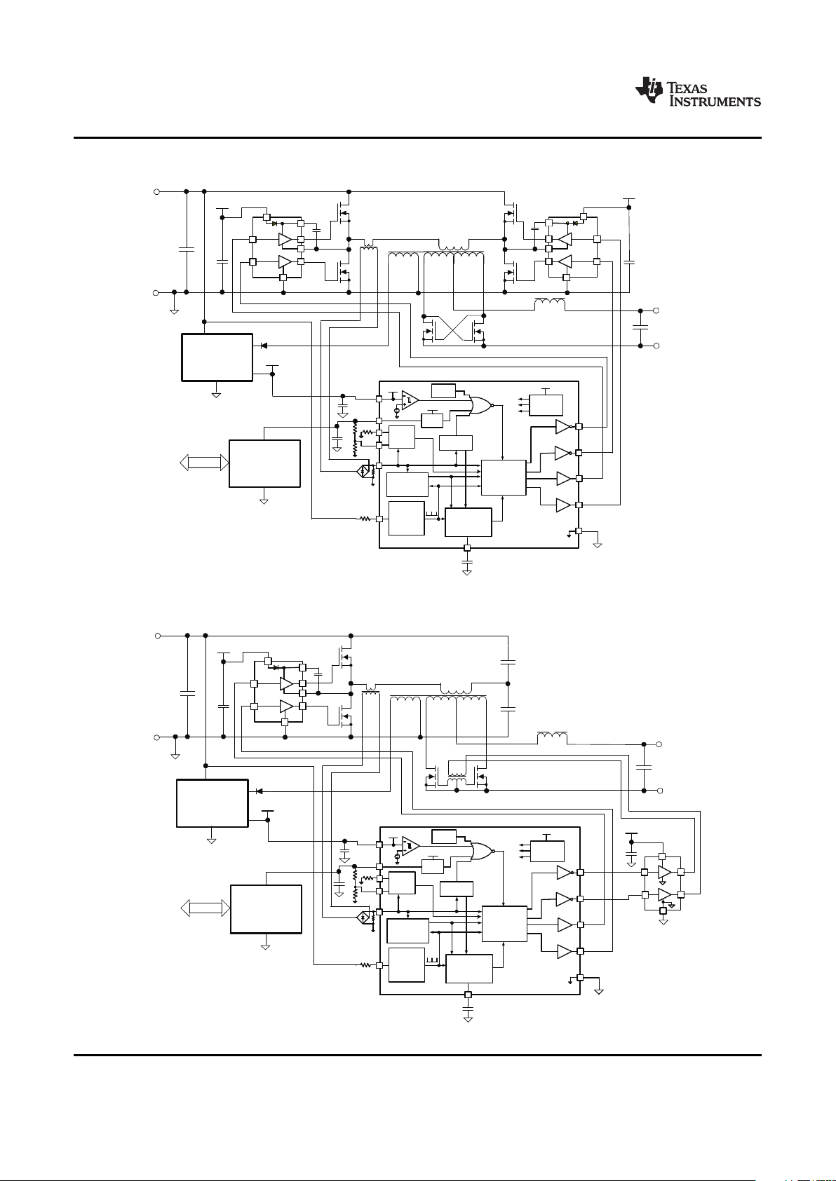
TYPICAL APPLICATION DIAGRAMS
Vin
36 Vto60V
+
_
CT
Vout
7 Vto12 V
400W
+
_
Vbias
Vbias
Vcc=5 Vor3.3V
Interface
with
System
HI
V
DD
V
SS
LI
HB
HO
HS
LO
HI
V
DD
V
SS
LI
HB
HO
HS
LO
UCC27200UCC27200
Bias
Power
Supply
Vbias
Housekeeping
Micro
Controller
GND
O1_D
VREF
V
DD
5V/3.3V
LDO
EN
UVLO
Comp.
6.3Vrise
5.7 Vfall
V
DD
V
DD
RT
CS
SS
Vin
OS
Thermal
Shutdown
Is
R1
R2
O2_DIN
O2_D
O1_DIN
8
10
11
9
7
1
2
6
4
12
SoftStart
&
HiccupCurrent
LimitCircuit
Logic
Block
V
DD
Reference
Generator
ShortCircuit
Shutdown
Oscillator
&
StartUp
Frequency
Control
Off Time
Control
Circuit
Cycle-by
-
CycleCurrent
Limit
CLK
3
OST
R3
5
Vin
36Vto60V
+
_
CT
Vout
7Vto12V
200W
+
_
Vbias
Houskeeping
Micro-
Controller
Vcc=5Vor3.3V
Interface
with
System
HI
V
DD
V
SS
LI
HB
HO
HS
LO
UCC27200
Bias
Power
Supply
Vbias
UCC28230/1
INA
2
4
7
5
6
3
V
DD
GND
INB
UCC27324
OUTA
OUTB
Vbias
GND
O1_D
VREF
V
DD
5V/3.3V
LDO
EN
UVLO
Comp.
6.3Vrise
5.7 Vfall
V
DD
V
DD
RT
CS
SS
Vin
OS
Thermal
Shutdown
Is
R1
R2
O2_DIN
O2_D
O1_DIN
8
10
11
9
7
1
2
6
4
12
SoftStart
&
HiccupCurrent
LimitCircuit
Logic
Block
V
DD
Reference
Generator
ShortCircuit
Shutdown
Oscillator
&
StartUp
Frequency
Control
Off Time
Control
Circuit
Cycle -by -
CycleCurrent
Limit
CLK
3
OST
R3
5
UCC28230
UCC28231
SLUS814A – FEBRUARY 2008 – REVISED JUNE 2008 ...................................................................................................................................................
www.ti.com
Figure 1. Full-Bridge Bus Converter
Figure 2. Half-Bridge Bus Converter with Control-Driven Synchronous Rectifier
2 Submit Documentation Feedback Copyright © 2008, Texas Instruments Incorporated
Product Folder Link(s): UCC28230 UCC28231

PINOUT CONFIGURATION
UCC28230
UCC28231
www.ti.com
................................................................................................................................................... SLUS814A – FEBRUARY 2008 – REVISED JUNE 2008
ORDERING INFORMATION
(1) (2)
TEMPERATURE RANGE,
REFERENCE VOLTAGE PACKAGE TAPE and REEL QTY PART NUMBER
TA= T
J
5 V .250 UCC28230DRNT
5 V 3000 UCC28230DRNR
Plastic 12-pin SON (DRN)
3.3 V 250 UCC28231DRNT
3.3 V 3000 UCC28231DRNR
– 55 ° C to +125 ° C
5 V 250 UCC28230PW
5 V 2000 UCC28230PWR
Plastic 14-pin TSSOP (PW)
3.3 V 250 UCC28231PW
3.3 V 2000 UCC28231PWR
(1) The 12-pin SON (DRN) and 14-pin TSSOP packages use Pb-Free lead finish of Pd-Ni-Au which is compatible with MSL level 1 at
255-260 ° C peak reflow temperature to be compatible with either lead free or Sn/Pb soldering operations.
(2) The pad underneath the center of the IC is a thermal substrate. The PCB “ thermal land ” design for this exposed die pad should include
thermal vias that drop down and connect to one or more buried copper plane(s). This combination of vias for vertical heat escape and
buried planes for heat spreading allows the DRN to achieve its full thermal potential. This pad is also internally connected to GND pin.
Copyright © 2008, Texas Instruments Incorporated Submit Documentation Feedback 3
Product Folder Link(s): UCC28230 UCC28231
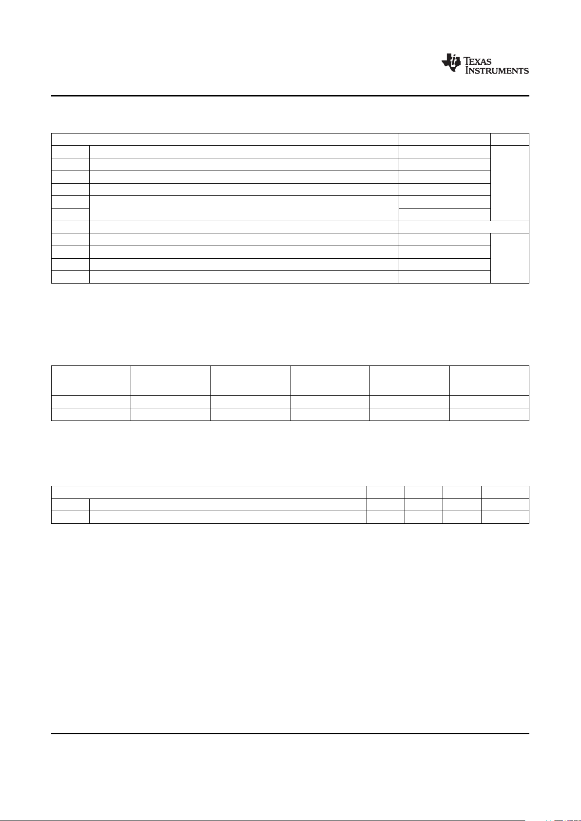
ABSOLUTE MAXIMUM RATINGS
DISSIPATION RATINGS
(1)
RECOMMENDED OPERATING CONDITIONS
UCC28230
UCC28231
SLUS814A – FEBRUARY 2008 – REVISED JUNE 2008 ...................................................................................................................................................
www.ti.com
over operating free-air temperature range
(1) (2)
(unless otherwise noted)
PARAMETER VALUE UNIT
V
DD
(3)
Input supply voltage range – 0.3 to 20.0
O1_D, O2_D, O1_DIN, O2_DIN – 0.3 to V
DD
+0.3
Inputs voltages on OS, CS, SS, RT, OST – 0.3 to 6.3
V
Output voltage on VREF – 0.3 to 5.6
HBM 2k
ESD rating
CDM 500
Continuous total power dissipation See Dissipation Rating Table
T
J
Operating virtual junction temperature range – 55 to +150
T
A
Operating ambient temperature range – 55 to +125
° C
T
stg
Storage Temperature – 65 to +150
Lead Temperature (Soldering, 10 sec.) PW Package +300
(1) Stresses beyond those listed under absolute maximum ratings may cause permanent damage to the device. These are stress ratings
only, and functional operation of the device at these or any other conditions beyond those indicated under recommended operating
conditions is not implied. Exposure to absolute-maximum-rated conditions for extended periods may affect device reliability.
(2) These devices are sensitive to electrostatic discharge; follow proper device handling procedures.
(3) All voltages are with respect to GND unless otherwise noted. Currents are positive into, negative out of the specified terminal. See
Packaging Section of the datasheet for thermal limitations and considerations of packages.
θJC( ° C/W) θJA( ° C/W) θJB( ° C/W)
θJP( ° C/W)
BOARD PACKAGE JUNCTION TO JUNCTION TO JUNCTION TO
JUNCTION TO PAD
CASE AMBIENT BOARD
High-K
(2)
DRN 70.66 15 37.66
PW 2.71 97.65 2.07
(1) These thermal data are taken at standard JEDEC test conditions and are useful for the thermal performance comparison of different
packages. The cooling condition and thermal impedance R
θ JA
of practical design is specific.
(2) The JEDEC test board JESD51-5 with direct thermal pad attach, 3-inch × 3-inch, 4-layer with 1-oz internal power and ground planes and
2-oz top and bottom trace layers (preliminary data based on modeling)
MIN NOM MAX UNIT
V
DD
Supply voltage range 7 12 17 V
Operating junction temperature range – 55 125 ° C
4 Submit Documentation Feedback Copyright © 2008, Texas Instruments Incorporated
Product Folder Link(s): UCC28230 UCC28231
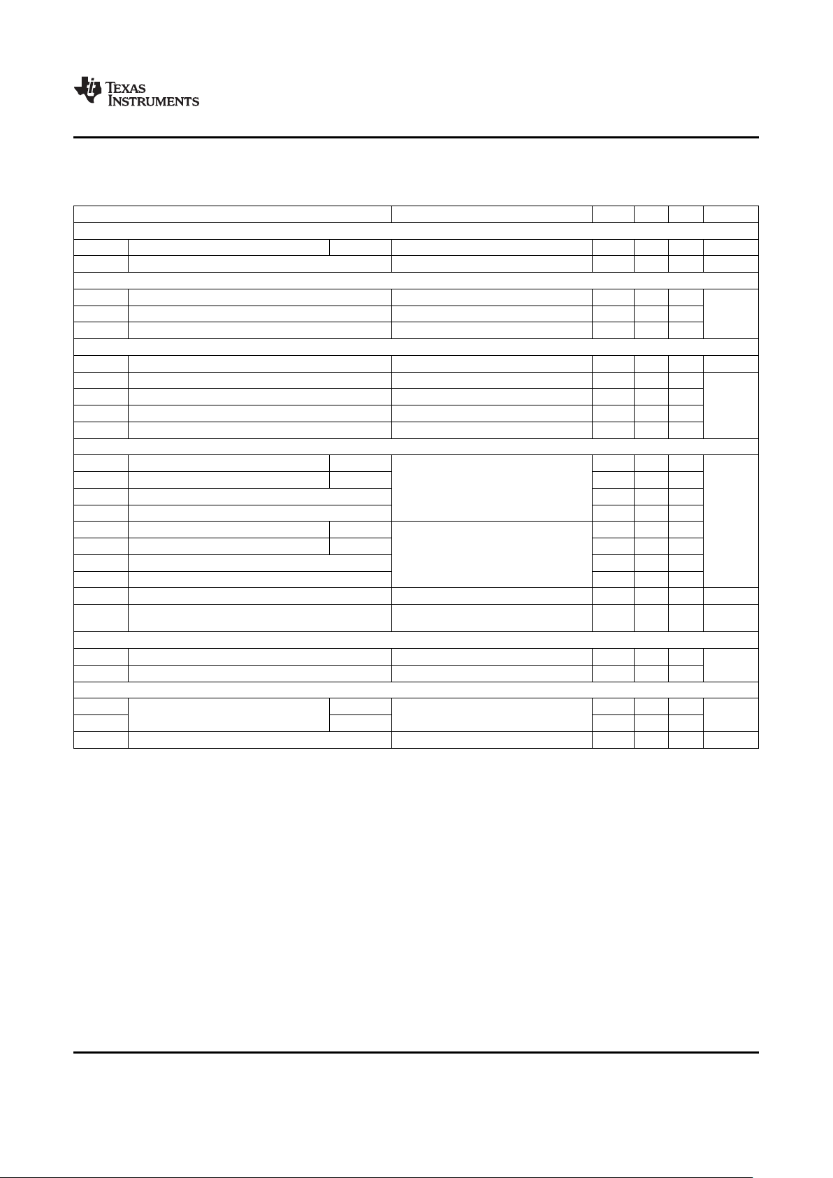
ELECTRICAL CHARACTERISTICS
(1)
UCC28230
UCC28231
www.ti.com
................................................................................................................................................... SLUS814A – FEBRUARY 2008 – REVISED JUNE 2008
V
DD
= 12V, 1- µ F capacitor from V
DD
and VREF to GND, TA= TJ= – 55 ° C to 125 ° C, RT = 49.9 k Ω connected to 4.4V supply to
set Fsw = 100 kHz (unless otherwise noted).
PARAMETER TEST CONDITIONS MIN TYP MAX UNIT
Supply Currents
ID
DD(off)
Startup current VDD= 5.2 V 150 200 µ A
I
DD
Operating supply current 1.5 2.5 mA
Under Voltage Lockout
Start threshold 5.9 6.3 6.9
Minimum operating voltage after start 5.3 5.7 6.2 V
Hysteresis 0.55 0.6 0.75
Soft Start (SS PIN, Figure 41 , Figure 44 )
I
SS
Charge current VSS= 0 V – 30 – 25 – 20 µ A
V
SS_STD
Shutdown/restart/reset threshold 0.3 0.55 0.68
V
SS_FP
Soft-start first pulse threshold 0.68 0.85 1.1
V
V
SS_PU
Pull up threshold 3.3 3.5 3.8
V
SS_CL
Clamp voltage 4.3 4.5 4.8
Off-Time Programming (Figure 33 )
T
OFF5
Off time between O1_D and O2_D UCC28230 32 40 50
T
OFF3
Off time between O1_D and O2_D UCC28231 30 40 53
OS = 8.45 k Ω , CS = 0.3 V, OST = 1 V
T
DT
Dead time between O1_D, O1_DIN and O2_D, O2_DIN 10 16
Δ T
OFF
Off time matching 2
ns
T
OFFR5
Off time between O1_D and O2_D UCC28230 32 40 50
T
OFFR3
Off time between O1_D and O2_D UCC28231 30 40 53
OS = 8.45 k Ω , CS = 0 V, OST = VREF
T
DTREF
Dead time between O1_D, O1_DIN and O2_D, O2_DIN 10 16
Δ T
OFFR
Off time matching 2
I
HYST
Hysteresis current source 10 µ A
OS = 8.45 k Ω , OST = 1 V, CS = CS
TH
– 0.03
T
OFFMAX
Maximum off time at low CS 165 235 ns
V
Switching Frequency at O1_D and O2_D Outputs
F
SWNOM
Nominal frequency VSS= 4 V 92 100 108
kHz
F
SWMAX
Maximum frequency VSS= 1.8 V 425 550 675
VREF Output Voltage
V
REF5
UCC28230 4.925 5 5.075
0 ≤ IR ≤ 10 mA; VDD= from 7 V to 17 V,
VREF total output range V
– 55 ° C ≤ TJ≤ 125 ° C
V
REF3
UCC28231 3.25 3.3 3.35
I
SCC
Short circuit current VREF = 0 V – 35 – 25 – 12 mA
(1) Typical values for TA= 25 ° C
Copyright © 2008, Texas Instruments Incorporated Submit Documentation Feedback 5
Product Folder Link(s): UCC28230 UCC28231
UCC28230
UCC28231
SLUS814A – FEBRUARY 2008 – REVISED JUNE 2008 ...................................................................................................................................................
www.ti.com
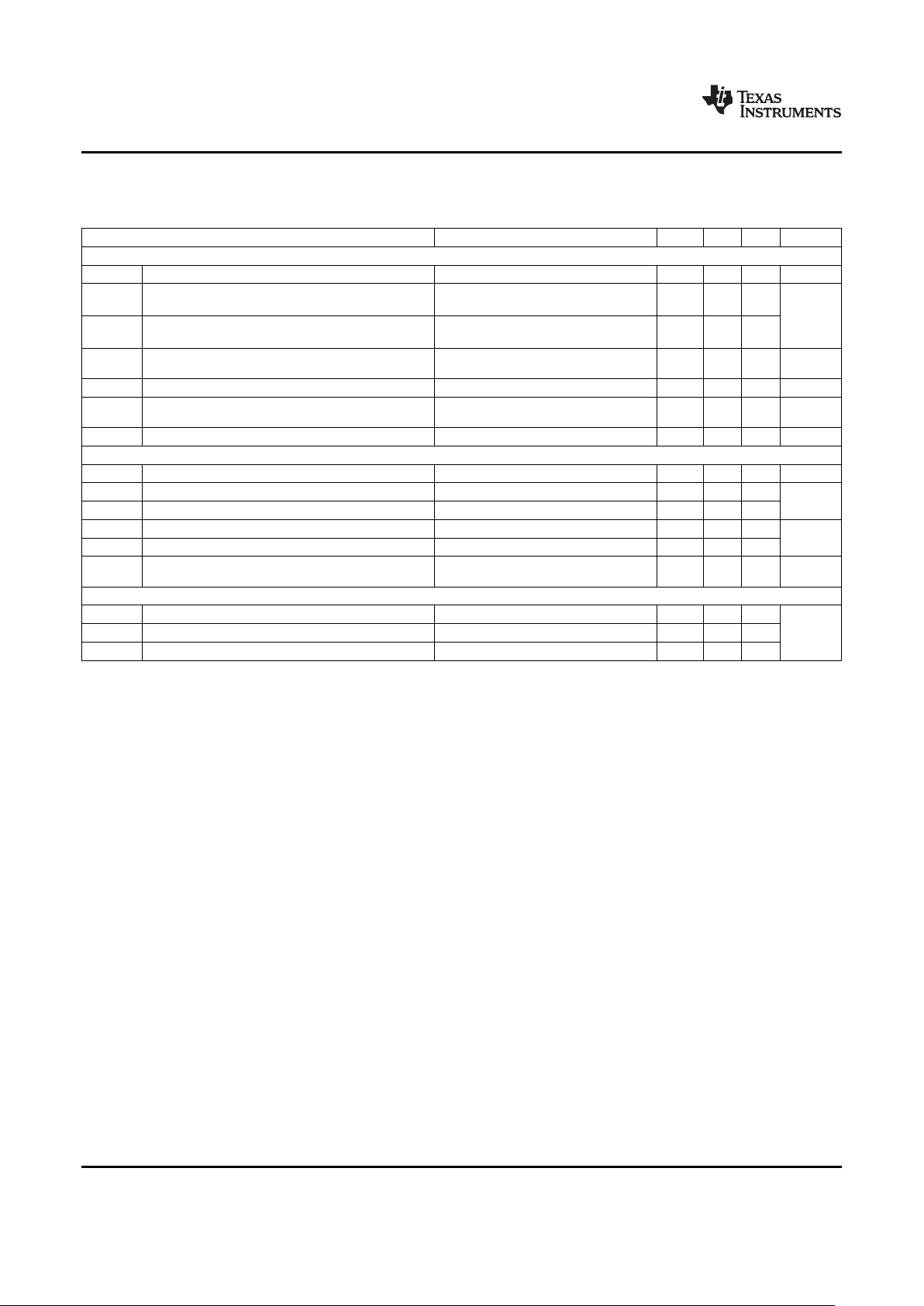
ELECTRICAL CHARACTERISTICS (continued)
V
DD
= 12V, 1- µ F capacitor from V
DD
and VREF to GND, TA= TJ= – 55 ° C to 125 ° C, RT = 49.9 k Ω connected to 4.4V supply to
set Fsw = 100 kHz (unless otherwise noted).
PARAMETER TEST CONDITIONS MIN TYP MAX UNIT
Current Sense, Cycle-by-Cycle Current Limit With Hiccup, Short Circuit Protection With Latch Off
V
CS_LIM
CS pin cycle-by-cycle threshold 0.48 0.5 0.515 V
Input pulse at CS from 0.3 V to 0.6 V with
T
CS
CS to O1_D and O2_D propagation delay 100
0.03 V/ns slew rate
ns
Input pulse at CS from 0.3 V to 0.6 V with
T
BL
Leading edge blanking time by internal filter 50
0.03 V/ns slew rate
Discharge current to set cycle-by-cycle current limit duration
I
DS
CS = 0.6 V, VSS= 4 V 15 20 25 µ A
(Figure 41 )
Hiccup OFF time threshold 3.1 3.4 3.7 V
Discharge current to set Hiccup Mode OFF Time
I
HCC
1.9 2.5 3.1 µ A
(Figure 41 , Figure 44 )
V
CS_SC
CS pin short circuit protection threshold (Figure 44 ) 0.65 0.7 0.75 V
Outputs O1_D, O2_D, O1_DIN, O2_DIN
Sink/Source peak current
(2)
0.2 A
Rise time C
LOAD
= 100 pF 12 25
ns
Fall time C
LOAD
= 100 pF 10 25
RSRC Output source resistance I
OUT
= 20 mA 10 20 35
Ω
RSINK Output sink resistance I
OUT
= 20 mA 5 15 30
Pins 7 and 9 pulses matching at FSW= 100
Duty cycle matching 35 ns
kHz
Thermal Shutdown
Rising threshold
(3)
150 160 170
Falling threshold
(3)
130 140 150 ° C
Hysteresis 20
(2) Output sink/source peak current value, defined by equation IP= 100 pF × dV/dt where dV/dt is taken from the output rise and fall
switching waveforms. It is not tested in production. Characterization is available upon request.
(3) Thermal shutdown is not tested in production. Characterization is available upon request
6 Submit Documentation Feedback Copyright © 2008, Texas Instruments Incorporated
Product Folder Link(s): UCC28230 UCC28231

FUNCTIONAL BLOCK DIAGRAMS
GND
O1_D
VREF
V
DD
5V/3.3V
LDO
EN
UVLO
Comp.
6.3V rise
5.7V fall
V
DD
V
DD
RT
CS
SS
Vin
CT
OS
Thermal
Shutdown
Is
R1
R2
O2_DIN
O2_D
O1_DIN
8
10
11
9
7
5
1
2
6
4
12
Soft Start &
Hiccup Current
Limit Circuit
Logic
Block
V
DD
Reference
Generator
Short Circuit
Shutdown
Oscillator &
Start Up
Frequency
Control
Off Time
Control
Circuit
Cycle-by-
Cycle Current
Limit
CLK
3
OST
R3
GND
O1_D
VREF
V
DD
5V/3.3V
LDO
EN
UVLO
Comp.
6.3V rise
5.7V fall
V
DD
V
DD
RT
CS
SS
Vin
CT
OS
Thermal
Shutdown
Is
R1
R2
O2_DIN
O2_D
O1_DIN
10
12
13
11
9
6
1
2
7
5
14
Soft Start &
Hiccup Current
Limit Circuit
Logic
Block
V
DD
Reference
Generator
Short Circuit
Shutdown
Oscillator &
Start Up
Frequency
Control
Off Time
Control
Circuit
Cycle-by-
Cycle Current
Limit
CLK
3
OST
R3
AGND
8
NC
4
UCC28230
UCC28231
www.ti.com
................................................................................................................................................... SLUS814A – FEBRUARY 2008 – REVISED JUNE 2008
Figure 3. SON-12 Package
Figure 4. TSSOP-14 Package
Copyright © 2008, Texas Instruments Incorporated Submit Documentation Feedback 7
Product Folder Link(s): UCC28230 UCC28231

UCC28230
UCC28231
SLUS814A – FEBRUARY 2008 – REVISED JUNE 2008 ...................................................................................................................................................
www.ti.com
TERMINAL FUNCTIONS
TERMINAL
I/O FUNCTION
DFN-12 TSSOP-14
NAME
PIN# PIN#
± 1.5% accurate 5 V for UCC28230 and 3.3 V for UCC28231, 10-mA output reference voltage with
short circuit protection that can be used for fixed switching frequency setting and/or for
1 1 VREF O
housekeeping microcontroller. Place decoupling capacitor in 1 µ F to 2.2 µ F range from this pin to
GND.
Off time control threshold pin uses a resistor divider to set current level as percentage of current
2 2 OST I
limit threshold.
Nominal off time T
OFF
and dead time TDTset pin. An external resistor connected between this pin
3 3 OS I
and GND sets the dead time and nominal off time.
4 NC Not connected pin, TSSOP-14 only.
Oscillator timing input pin. The external resistor which is connected between this pin and VINsets
4 5 RT I the oscillator frequency which varies with VIN. Tying the external resistor to VREF sets fixed
frequency operation independent of VIN.
Input to adjustable soft-start,and hiccup mode circuit. Place soft-start capacitor from this pin to
5 6 SS I/O GND. The internal charge/discharge current ISSand an external capacitor value set the soft-start
timing, duration of cycle-by-cycle current limit and controller turn-off time for hiccup mode operation.
6 7 CS I Current sensing pin used for cycle-by-cycle current limit, short circuit protection and off time control.
8 AGND Analog ground, TSSOP-14 only.
7 9 GND Ground pin connected to thermal pad. All signals are referenced to this node.
8 10 O2_DIN O 0.2-A sink/source switching output pin to an external driver providing 1-D pulse.
9 11 O2_D O 0.2-A sink/source switching output pin to an external driver providing D pulse.
10 12 O1_DIN O 0.2-A sink/source switching output pin to an external driver providing 1-D pulse.
11 13 O1_D O 0.2-A sink/source switching output pin to an external driver providing D pulse.
Connect this pin to a 7-V to 17-V bias supply. Place a high quality at least 1- µ F ceramic bypass
12 14 VDD I
capacitor from this pin to GND.
8 Submit Documentation Feedback Copyright © 2008, Texas Instruments Incorporated
Product Folder Link(s): UCC28230 UCC28231
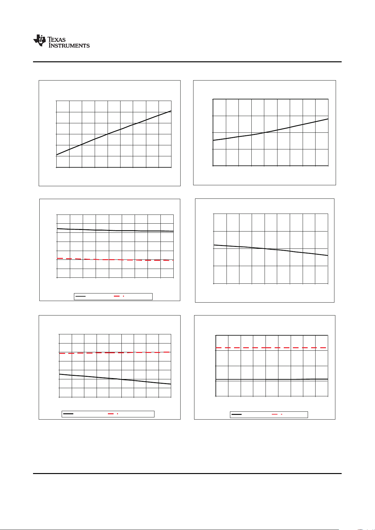
TYPICAL CHARACTERISTICS
Operating Supply Current I
DD
over Temperature at FSW=100kHz
1.40
1.45
1.50
1.55
1.60
-55 -35 -15 5 25 45 65 85 105 125
TJ-tempe rature, °C
I
DD,
mA
Start-up Current I
DDoff
over Temperature at VDD=5.2V
135
140
145
150
155
160
165
-55 -35 -15 5 25 45 65 85 105 125
TJ-tempera ture, °C
I
DDo ff,,
µA
Under Voltage Lockout Thresholds
over Temperature
5.3
5.5
5.7
5.9
6.1
6.3
6.5
6.7
-55 -35 -15 5 25 45 65 85 105 125
TJ-temperature, °C
UVLO Thresholds, V
Rising threshold
Falling threshold
Under Voltage Lockout Hysteresis
over Temperature
0.62
0.64
0.66
0.68
0.70
-55 -35 -15 5 25 45 65 85 105 125
TJ-temperature, °C
UVLO Hysteresis, V
Soft Start Shutdown V
SS_STD
and First Pulse V
SS_FP
Thresholds over Temperature
0.30
0.40
0.50
0.60
0.70
0.80
0.90
1.00
-55 -35 -15 5 25 45 65 85 105 125
TJ-te mperature, ° C
V
SS_STD
, V
SS_FP
, V
Soft Start Shutdown
First Puls e Threshold
Soft Start Pull-up V
SS_PU
and Clamp Voltage V
SS_CL
Thresholds over Temperature
3.00
3.50
4.00
4.50
5.00
-55 -35 -15 5 25 45 65 85 105 125
TJ-te mperature, ° C
V
SS_PU
, V
SS_CL
, V
Pull-up Threshold
Clamp Voltage
UCC28230
UCC28231
www.ti.com
................................................................................................................................................... SLUS814A – FEBRUARY 2008 – REVISED JUNE 2008
Figure 5. Figure 6.
Figure 7. Figure 8.
Figure 9. Figure 10.
Copyright © 2008, Texas Instruments Incorporated Submit Documentation Feedback 9
Product Folder Link(s): UCC28230 UCC28231

Soft-Start Charge Current I
SS
over Temperature
24.80
24.85
24.90
24.95
25.00
25.05
25.10
25.15
25.20
-55 -35 -15 5 25 45 65 85 105 125
TJ-temperature, °C
Iss, µA
OffTimeMatching ∆T
OFF
overTemperature
1.00
1.50
2.00
2.50
3.00
3.50
4.00
-55 -35 -15 5 25 45 65 85 105 125
TJ-temperature,°C
∆T
OFF
,ns
UCC28230 Off Time T
OFF
and Dead Time T
DT
over Temperature
10
20
30
40
50
-55 -35 -15 5 25 45 65 85 105 125
TJ- te mperature, °C
T
OFF
, T
DT
, ns
Off Time
Dead Time
UCC28231 Off Time T
OFF
and Dead Time T
DT
over T emperature
10
20
30
40
50
-55 -35 -15 5 25 45 65 85 105 125
TJ- tempe rature, °C
T
OFF
, T
DT
, ns
Off Time
Dead Time
Maximum Off Time T
OFFMAX
at Low V
CS
over Temperature
170.00
180.00
190.00
200.00
210.00
220.00
-55 -35 -15 5 25 45 65 85 105 125
TJ- te mperatu re, °C
T
OFFM AX
, ns
Nominal Switching Frequency F
SWNOM
over Temperature
99.00
99.50
100.00
100.50
101.00
-55 -35 - 15 5 25 45 65 85 105 125
TJ- te mperature, ° C
F
SWNOM
, kHz
UCC28230
UCC28231
SLUS814A – FEBRUARY 2008 – REVISED JUNE 2008 ...................................................................................................................................................
www.ti.com
TYPICAL CHARACTERISTICS (continued)
Figure 11. Figure 12.
Figure 13. Figure 14.
Figure 15. Figure 16.
10 Submit Documentation Feedback Copyright © 2008, Texas Instruments Incorporated
Product Folder Link(s): UCC28230 UCC28231
Maximum Switching Frequency F
SWMAX
over Temperature
500.00
510.00
520.00
530.00
540.00
550.00
-55 -35 - 15 5 25 45 65 85 105 125
TJ- temperature , °C
FSWMAX , kHz
Cycle-by-Cycle Current Limit Threshold
over Temperature
0.45
0.47
0.49
0.51
0.53
0.55
-55 -35 -15 5 25 45 65 85 105 125
TJ-tempera ture, °C
V
CS_LIM
, V
UCC28230 Refer ence Voltage at VDD=12V
over Te mperature and Load Curr ent
4.9 75
4.9 85
4.9 95
5.0 05
5.0 15
-55 -3 5 - 15 5 2 5 45 65 8 5 105 125
TJ- te mper ature, °C
V
REF
, V
Iload=10uA
Iload=1mA Iload=10mA
UCC28231 Refer ence Voltage at VDD=12V
over Te mperature and Load Curr ent
3.2 75
3.2 85
3.2 95
3.3 05
-55 -35 - 15 5 2 5 45 65 85 105 1 25
T
J
- te mper ature, °C
V
REF
, V
Iload=10uA
Iload=1mA Iload=10mA
UCC28230 Refer ence Voltage at I
LOAD
=1mA
over Te mper ature and Supply Voltage V
DD
4.990
4.994
4.998
5.002
5.006
-55 - 35 -15 5 25 45 65 85 105 125
TJ- te mper ature, °C
V
REF
, V
Vdd=7V
Vdd=12V Vdd=17V
UCC28231 Refer ence Voltage at I
LOAD
=1mA
over Te mperature and Supply Voltage V
DD
3.2 90
3.2 94
3.2 98
3.3 02
3.3 06
-55 -35 -1 5 5 25 45 65 8 5 105 1 25
TJ- te mper ature, °C
V
REF
, V
Vdd=7V
Vdd=12V Vdd=17V
UCC28230
UCC28231
www.ti.com
................................................................................................................................................... SLUS814A – FEBRUARY 2008 – REVISED JUNE 2008
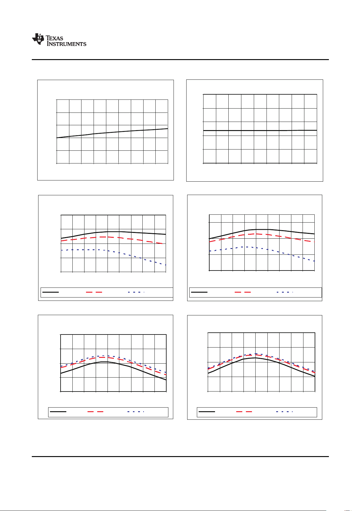
TYPICAL CHARACTERISTICS (continued)
Figure 17. Figure 18.
Figure 19. Figure 20.
Figure 21. Figure 22.
Copyright © 2008, Texas Instruments Incorporated Submit Documentation Feedback 11
Product Folder Link(s): UCC28230 UCC28231
Current Sense Propogation Delay T
CS
over Temperature
90.00
95.00
100.00
105.00
110.00
115.00
-55 -35 - 15 5 25 45 65 85 105 125
TJ- te mperatu re, °C
T
CS
, ns
Output Source Resistance R
SRC
and Sink Resistance
R
SINK
over Temperature
10.0
15.0
20.0
25.0
30.0
-55 -35 -15 5 25 45 65 85 105 125
TJ- te mperatur e, °C
R
SCR
, R
SINK
, O
Source Resistance
Sink Resist ance
UCC28230
UCC28231
SLUS814A – FEBRUARY 2008 – REVISED JUNE 2008 ...................................................................................................................................................
www.ti.com
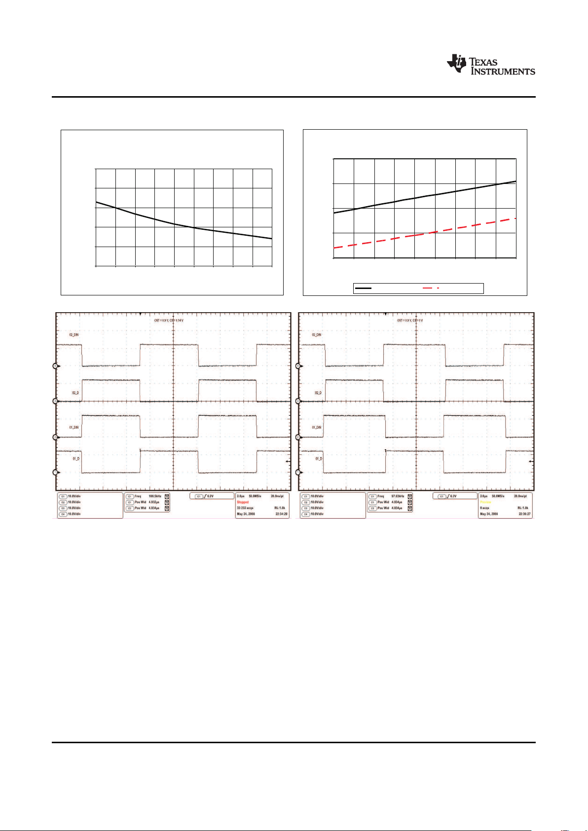
TYPICAL CHARACTERISTICS (continued)
Figure 23. Figure 24.
Figure 25. O1_D and O2_D Duty Cycle Matching at V
CS
= Figure 26. O1_D and O2_D Duty cycle Matching at V
CS
=
0.14 V and V
OST
= 1 V 0.0 V and V
OST
= 1 V
12 Submit Documentation Feedback Copyright © 2008, Texas Instruments Incorporated
Product Folder Link(s): UCC28230 UCC28231
UCC28230
UCC28231
www.ti.com
................................................................................................................................................... SLUS814A – FEBRUARY 2008 – REVISED JUNE 2008
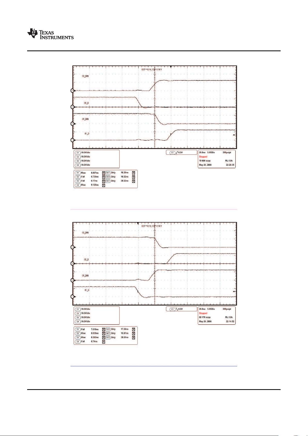
TYPICAL CHARACTERISTICS (continued)
Figure 27. Output Waveforms During First Half Switching Cycle at V
CS
= 0.14 V and V
OST
= 1 V
Figure 28. Output Waveforms During Second Half Switching Cycle at V
CS
= 0.14 V and V
OST
= 1 V
Copyright © 2008, Texas Instruments Incorporated Submit Documentation Feedback 13
Product Folder Link(s): UCC28230 UCC28231
UCC28230
UCC28231
SLUS814A – FEBRUARY 2008 – REVISED JUNE 2008 ...................................................................................................................................................
www.ti.com
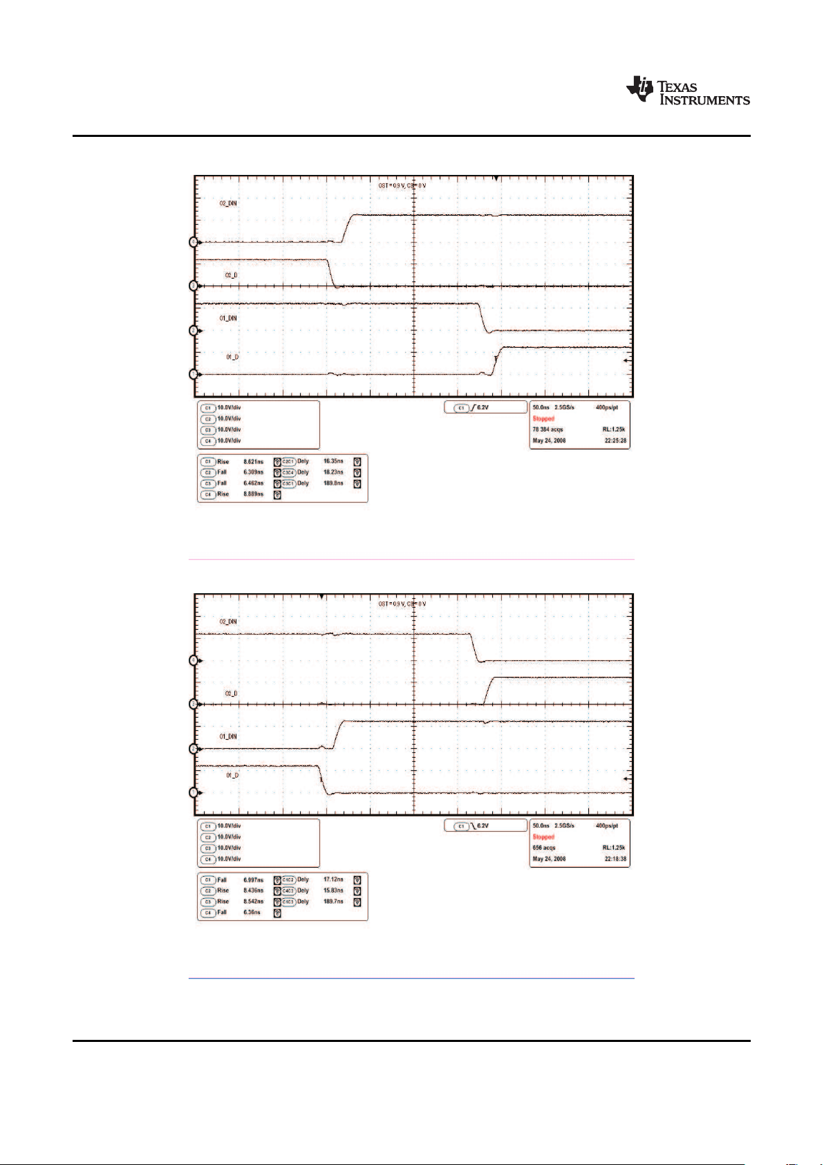
TYPICAL CHARACTERISTICS (continued)
Figure 29. Output Waveforms During First Half Switching Cycle at V
CS
= 0 V and V
OST
= 1 V
Figure 30. Output Waveforms During Second Half Switching Cycle at V
CS
= 0 V and V
OST
= 1 V
14 Submit Documentation Feedback Copyright © 2008, Texas Instruments Incorporated
Product Folder Link(s): UCC28230 UCC28231
 Loading...