

Page 1
Switch Mode Secondary Side Post Regulator
UCC1583
UCC2583
UCC3583
FEATURES
Precision Secondary Side Post
•
Regulation for Multiple Output Power
Supplies
Useful for Both Single Ended and
•
Center Tapped Secondary Circuits
Ideal Replacement for Complex
•
Magnetic Amplifier Regulated Circuits
Leading Edge Modulation
•
Does Not Require Gate Drive
•
Transformer
High Frequency (>500kHz) Operation
•
Applicable for Wide Range of Output
•
Voltages
• High Current Gate Driver (0.5A
Sink/1.5A Source)
• Average Current Limiting Loop
DESCRIPTION
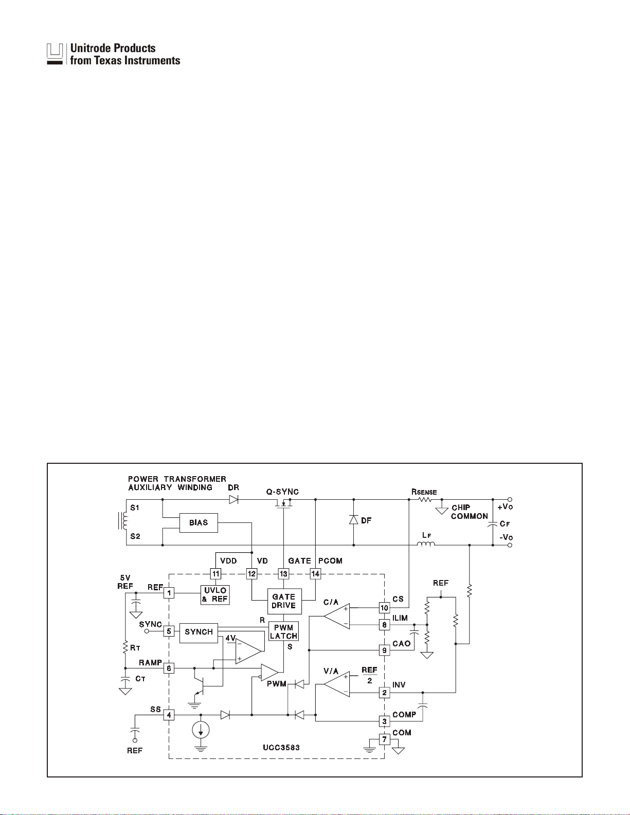
The UCC3583 is a synchronizable secondary side post regulator for preci
sion regulation of the auxiliary outputs of multiple output power supplies. It
contains a leading edge pulse width modulator, which generates the gate
drive signal for a FET power switch connected in series with the rectifying
diode. The turn-on of the power switch is delayed from the leading edge of
the secondary power pulse to regulate the output voltage. The UCC3583
contains a ramp generator slaved to the secondary power pulse, a voltage
error amplifier, a current error amplifier, a PWM comparator and associ
ated logic, a gate driver, a precision reference, and protection circuitry.
The ramp discharge and termination of the gate drive signal are triggered
by the synchronization pulse, typically derived from the falling edge of the
transformer secondary voltage. The ramp starts charging again once its
low threshold is reached. The gate drive signal is turned on when the ramp
voltage exceeds the control voltage. This leading edge modulation tech
nique prevents instability when the UCC3583 is used in peak current mode
primary controlled systems.
The controller operates from a floating power supply referenced to the output voltage being controlled. It features an undervoltage lockout (UVLO)
circuit, a soft start circuit, and an averaging current limit amplifier. The current limit can be programmed to be proportional to the output voltage, thus
achieving foldback operation to minimize the dissipation under short circuit
conditions.
-
-
-
TYPICAL APPLICATION AND BLOCK DIAGRAM
(continued)
Note: Pin connections shown for 14-pin packages.
SLUS299B - OCTOBER 1998 - REVISED JANUARY 2005
UDG-96201-2
Page 2
ABSOLUTE MAXIMUM RATINGS
VDD.......................................... 15V
I
.........................................15mA
VDD
RAMP .............................–0.3V to V
I
.........................................5mA
RAMP
I
....................................................
REF
P
COM ..................................–0.2V to 0.2V
I
(twp < 1µS and Duty Cycle < 10%) ...... –0.8A to 1.8A
GATE
I
..................................–5mA to 5mA
COMP
I
...................................–5mA to 5mA
CAO
V
............................–0.6V to V
SYNC
I
.................................–05mA to 5mA
SYNC
REF
+1V
DD
–30mA
+0.3V
INV, SS, ILIM, ISENSE..............–0.3V to VREF + 0.3V
Storage Temperature ...................–65°C to +150°C
Junction Temperature...................–55°C to +150°C
Lead Temperature (Soldering, 10 sec.) .............+300°C
All voltages are with respect to the COM terminal unless other
wise stated. Currents are positive into, negative out of the
specified terminal. Consult Packaging Section of Databook for
thermal limitations and considerations of packages.
THERMAL IMPEDANCE
PACKAGE qja qjc
N-14 90 45
J-14 90-120 28
D-14 50-120 35
PLCC-20 43-75 34
UCC1583
UCC2583
UCC3583
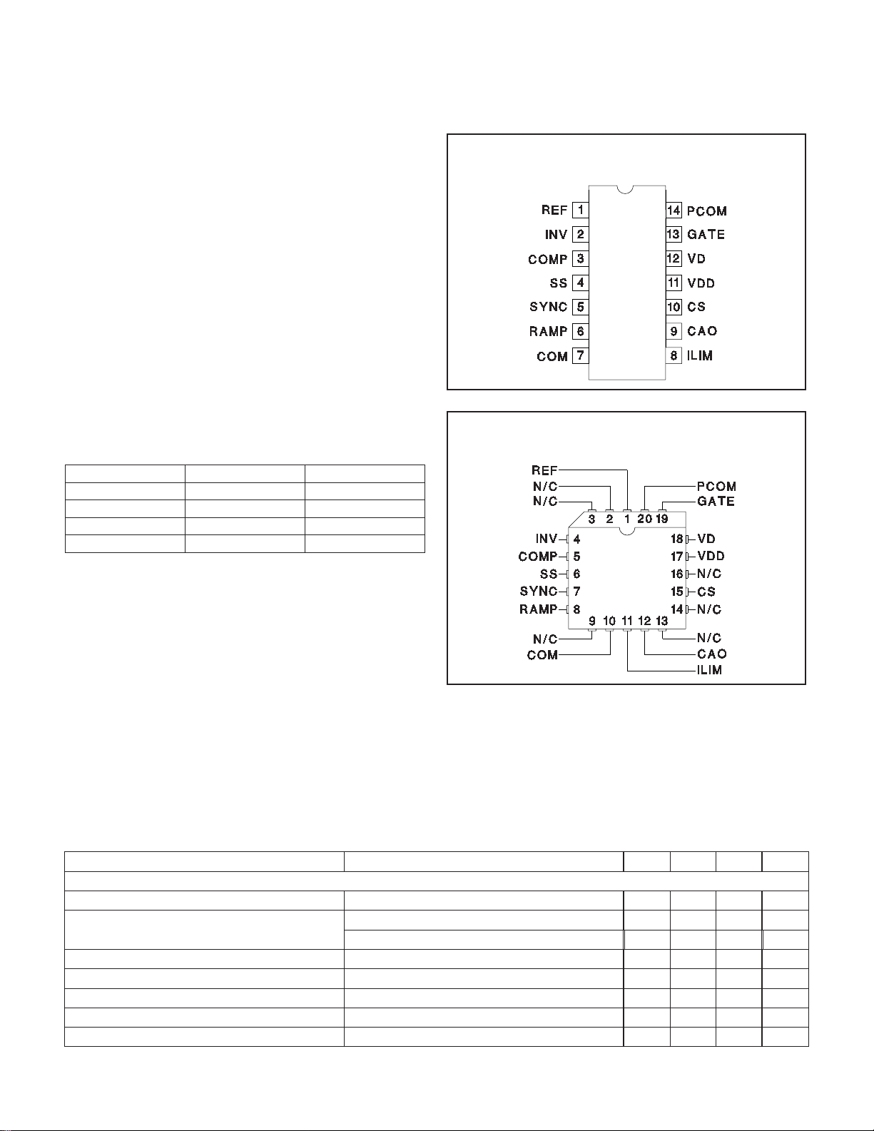
CONNECTION DIAGRAMS
DIL-14, SOIC-14 (Top View)
J, N, or D Packages
-
PLCC-20 (Top View)
Q Package
Note 1. qja (junction to ambient) is for devices mounted to 5 in2
FR4 PC board with one ounce copper where noted. When resistance range is given, lower values are for 5 in2 aluminum
PC board. Test PWB was .062 in thick and typically used 0.635
mm trace widths for power pkgs and 1.3 mm trace widths for
non-power pkgs with a 100x100 mil probe land area at the end
of each trace
Note 2. qjc data values stated were derived from
MIL-STD-1835B. MIL-STD-1835B states that “The baseline
values shown are worst case (mean + 2s) for a 60x60 mil
microcircuit device silicon die and applicable for devices with
die sizes up to 14400 square mils. For device die sizes greater
than14400 square mils use the following values; dual-in-line,
11°C/W; flat pack, 10°C/W; pin grid array, 10°C/W”.
ELECTRICAL CHARACTERISTICS:Unless otherwise stated, these specifications apply for T
UCC1583, –40°C to 85°C for UCC2583, and 0°C to 70°C for UCC3583; VDD = 12V, R
= 60k, CT= 100pF, TA=TJ.
T
= –55°Cto125°C for
A
PARAMETER TEST CONDITIONS MIN TYP MAX UNITS
Ramp Generation and Synchronization
Maximum Input Operating Frequency For input with 5% to 90% duty cycle (Note 1) 500 kHz
Ramp Frequency, Free Running T
Ramp Discharge Current V
= 25°C 95 100 105 kHz
A
T
= -55°C to 125°C 90 100 110 kHz
A
= 0.5V 2.0 3.6 mA
RAMP
Low Threshold Voltage No min, no max, 0=TYP 0 V
High Threshold Voltage 3.75 4 4.25 V
Synchronizing Threshold Voltage (On) (Note 1) 1 V
Synchronizing Comparator Hysteresis 1 V
2
Page 3

UCC1583
UCC2583
UCC3583
ELECTRICAL CHARACTERISTICS:
UCC1583, –40°C to 85°C for UCC2583, and 0°C to 70°C for UCC3583; VDD = 12V, R
Unless otherwise stated, these specifications apply for TA= –55°Cto125°C for
= 60k, CT= 100pF, TA=TJ.
T
PARAMETER TEST CONDITIONS MIN TYP MAX UNITS
Output Duty Cycle
Minimum Duty Cycle Output D/C = Output PW / Input PW 0 %
Maximum Duty Cycle Output D/C = Output PW / Input PW 100 %
Voltage Error Amplifier
V
INV
I
INV
Low V
V
COMP
V
High V
COMP
V
=VINV, 0°C to 70°C (UCC3583) 2.462 2.5 2.538 V
COMP
V
=VINV, All Other Temperature Ranges 2.45 2.5 2.55 V
COMP
V
=VINV 300 500 nA
COMP
= 2.6V, ICOMP = 100µA 450 700 mV
INV
= 2.4V, ICOMP = –100µA 5.0 5.5 6.0 V
INV
AVOL No Load 70 90 dB
GBW Product At f = 100kHz, T
A = 25°C (Note 1) 3 5 MHz
Current Error Amplifier
Input Offset Voltage 10 mV
Input CM Low Common Mode for CS and ILIM (Note 1) 0 V
Input CM High Common Mode for CS and ILIM (Note 1) 2 V
V
Low V
CAO
V
High V
CAO
+IN
+IN
= 0V, V
= 0V, V
= 0.1V, ICAO = 100µA 250 500 mV
–IN
= 0.1V, ICAO = –100µA 5.0 5.5 6.0 V
–IN
Input Current (ILIM and CS Pins) –50 0 50 nA
AVOL No Load 70 90 dB
GBW Product At f = 100kHz, T
= 25°C 2 4 MHz
A
Soft Start Current 10 25 µA
UVLO
VDD On Threshold Voltage 8.5 9.0 9.5 V
VDD Off Threshold Voltage 7.9 8.4 8.9 V
UVLO Hysteresis 0.3 0.6 0.9 V
Bias Supply
Supply Clamp Voltage 13 14 15 V
Supply Current (VDD) f = 100kHz With No Gate Output Load 3 5 mA
Output Driver
V
SAT High I
SAT Low IGATE = 50mA 0.4 0.75 V
V
Rise Time C
Fall Time C
= –150mA 0.6 1.0 V
GATE
GATE = 1nF 50 75 ns
GATE = 330pF 20 40 ns
Reference
REF IREF = 0, 0°C to 70°C (UCC3583) 4.925 5 5.075 V
V
I
REF = 0, All Other Temperature Ranges 4.900 5 5.100 V
Line Regulation VDD = 10V to 14V 2 30 mV
Load Regulation I
REF = 0mA to 2mA 1 20 mV
Note 1: Ensured by design. Not 100% tested in production.
3
Page 4

PIN DESCRIPTIONS
CAO: Output of the current error amplifier. Averaging of
the sensed current signal is provided by connecting an
integrating capacitor between ILIM and CAO. CAO feeds
into the PWM comparator input and controls the loop
when its voltage is higher than the voltage at COMP
(output of the voltage error amplifier).
COM: Signal ground for the chip. It is connected to the
positive terminal of the output voltage being regulated by
the IC.
COMP: Output of the voltage error amplifier fed into the
PWM comparator. Loop compensation components are
connected between COMP and INV.
CS: Non-inverting input of the current error amplifier. The
sensed current signal from the current sense resistor is
connected to this pin. By making the signal at CS
proportional to the output voltage, effective current
foldback limiting can be provided.
GATE: Gate drive output for the power switch FET. The
drive pin has a 0.5A sink/1.5A source capability and very
low output off-state impedance.
ILIM: Inverting input of the current error amplifier. It sets
the DC limit for the output current.
INV: Inverting input of the voltage error amplifier. The
feedback signal is connected to this pin using a resistive
divider between REF and –V
PCOM: Power ground for the chip. It is connected to the
source terminal of the MOSFET being regulated by the
IC.
RAMP: This pin is the input to the PWM comparator and
provides a ramp signal for generation of the PWM signal.
A capacitor to COM and a resistor to REF set the
charging rate for the ramp. An internal current source of
O.
UCC1583
UCC2583
UCC3583
1mA discharges RAMP when synchronization signal
appears or when RAMP crosses a 4V threshold. In the
intended mode of operation, the switching frequency is
determined by the secondary power pulse. The RC
components at RAMP should be selected to give an
appropriately sized ramp signal. In the absence of a
synchronizing pulse, these RC components determine
the free running frequency of the controller.
REF: Precision 5V reference pin. REF stays off until VDD
exceeds 9V and turns off again when VDD drops below
8.4V. Bypass REF to COM.
SS: This pin provides a soft start function. A capacitor to
REF programs the soft start time. During soft start, the
PWM comparator is controlled by the soft start voltage
resulting in a slow increase in output duty cycle. Once
the soft start capacitor is discharged, output control is
dictated by the larger of the output at CAO or COMP.
SYNC: Synchronization input pin. It is connected to a
signal representative of the secondary power pulse. One
possible implementation is to use a resistive divider
between terminal S2 of the secondary winding shown in
Figure 1 and REF for generating the input to the SYNC
pin. The synchronizing comparator is referenced to 0.5V
and has ±500mV of hysteresis. The trip levels are
approximate 1.0V and 0.0V. The designer should prevent
the SYNC pin from exceeding 0.3V below ground as this
will turn on the ESD diode.
VD: Power supply for the output driver. VD should be tied
to VDD in the application.
VDD: Power supply for the chip. VDD should be
bypassed to COM. VDD has to be 9V for the IC to start
and 8.4V for it to remain operational. A shunt clamp from
VDD to COM limits the supply voltage to 14V.
APPLICATION INFORMATION
Power Stage Circuit Configuration
The UCC3583 is designed for use in a post regulator ap
plication for tightly regulating auxiliary outputs in a multi
ple output converter. The post regulation is applied to the
secondary side power pulse of a power transformer
where the power pulse is controlled by the feedback sig
nal from the main output. In order to simplify the applica
tion of the UCC3583, it is required that the IC be
referenced to the positive output terminal and the output
filter inductor be placed in the return path. The placement
of the inductor in the return path facilitates better EMI
performance, in addition to making magnetic designs
and terminations easier to implement. Typical set-up and
circuit waveforms of the UCC3583 system application
are shown in Figure 1. Figure 2 shows waveforms for a
single ended output rectifier application of the UCC3583
shown on page 1. The UCC3583 can also be used in
half bridge rectifier applications as shown by the circuit
and waveforms depicted in Figures 3 and 4. Referencing
the IC to the positive output terminal creates a require
ment for a floating bias voltage for the IC which can be
referenced to the same positive voltage terminal. Possi
ble implementations of deriving the floating bias voltage
are shown in Figure 5.
4
-
-
Page 5

APPLICATION INFORMATION (cont.)
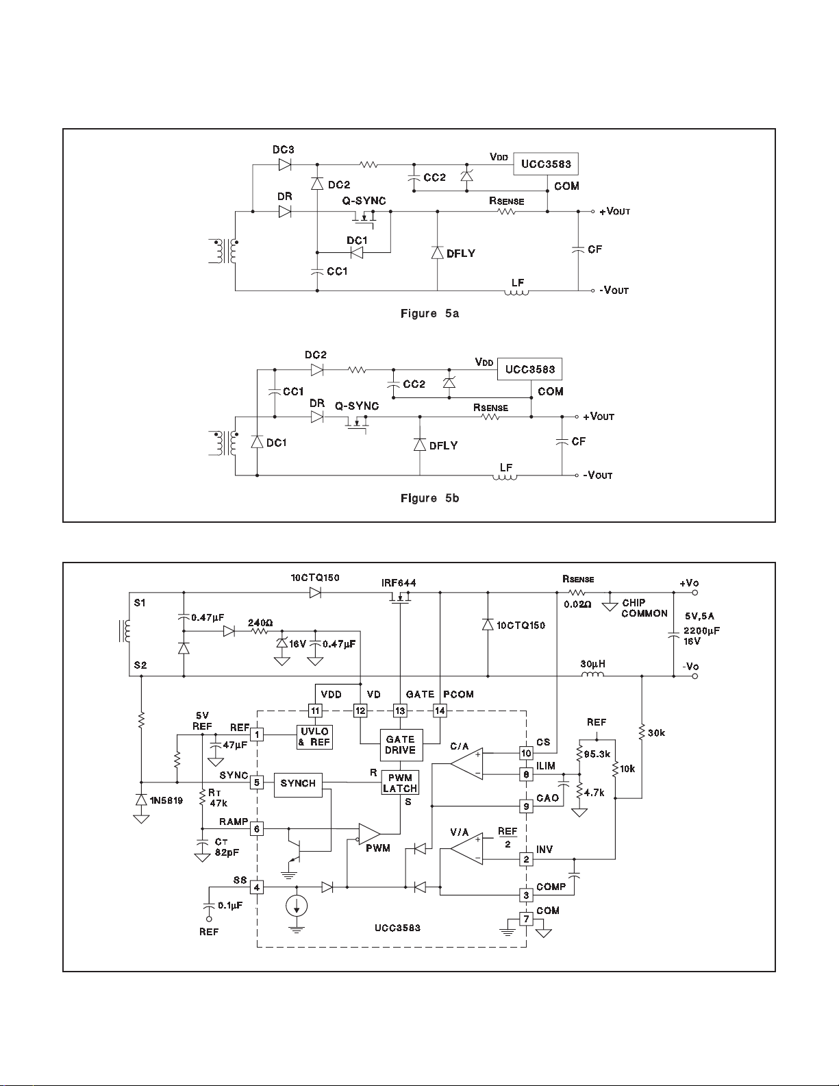
For the circuit shown in Figure 5a, CC1 is charged when
the transformer voltage is positive and the synchronous
switch is on. During the off period of Q-SYNC, the charge
is transferred to CC2 through diode DC2. Diode DC3
charges CC2 during the blocking interval of Q-SYNC.
This method is preferable when the transformer positive
voltage is high enough to generate the required bias volt
age. For the circuit shown in Figure 5b, CC1 is charged
during the period when reverse (reset) voltage appears
across the secondary. The charge on CC1 is transferred
to CC2 through DC2 when Q-SYNC turns on. This
method is preferable when the reverse voltage is high
enough to generate the required bias voltage. The series
resistor should be chosen to handle the required voltage
drop at full IC operating current when the zener clamp
across VDD and COM is activated.
The following is a description of the major functional
blocks of the UCC3583. Refer to Figure 6 (Typical Appli
cation Circuit) for component designations.
UVLO and Start Up
The UCC3583 has an internal undervoltage lockout circuit which keeps the internal circuitry inactive until VDD
exceeds the upper threshold (9V). Once the chip is activated, VDD has to be above the lower UVLO threshold
(8.4V) for it to remain functional. The IC requires a low
startup current of only 100µA when VDD is under the
UVLO threshold. VDD has an internal clamp of 14V
which can sink up to 10mA. Measures must be taken not
to exceed this current. The internal reference (REF) is
brought up when the UVLO on threshold is exceeded.
The soft start pin provides an effective means to start the
IC in a controlled manner. An internal current of 10µA
starts discharging a capacitor connected to SS when the
UVLO conditions have been removed. The voltage on
SS controls the duty cycle of the output during the dis
charge period.
Synchronizing Circuit and Oscillator
UCC3583 is primarily intended for synchronizable opera
tion where its switching frequency is determined by the
secondary pulse of the power transformer. However, it
has an internal oscillator which allows it to operate in
free-running mode when an external synchronization
pulse is not available. The switching frequency is deter
mined by resistor R
RAMP and capacitor C
The frequency is given by:
freq
1
=
tt
+
CH DIS
and
T connected between REF and
T connected from RAMP to GND.
where t R C
=••
156.
CH T T
UCC1583
UCC2583
UCC3583
CV
•
DIS
=
T
I
RAMP dis
t
The values of R
the ramp is discharged through an internal impedance of
2k. The value of R
-
that the internal discharge current is the current through
T during the entire discharge period. This results in
R
making the value of C
quency of operation.
When the synchronizing signal is available, the oscillator
frequency should be programmed to be lower than the
synchronizing frequency to ensure proper operation. A
large difference in self-running and synchronizing fre
quencies leads to smaller ramp amplitude and higher
noise sensitivity. The ramp capacitor is discharged when
the synchronization signal arrives and begins charging
-
when the low threshold is crossed.
There are two methods to synchronize to the secondary
pulse. One method is to use the rising edge of the secondary pulse, which reduces the maximum duty cycle
available. Subsequently, the post regulator switch cannot
be turned on during the C
method is to use the falling edge of the secondary pulse
for synchronization. This method is preferable because it
allows a slower discharge of the ramp capacitor without
affecting the maximum available duty cycle of the post
regulator. The UCC3583 SYNC input needs to reach a
fixed threshold (1.0V typical) for synchronization to take
effect. Hence the IC is usable with either method of syn
chronization. However, the UCC3583 oscillator configu
ration is better suited for synchronization to the falling
edge. A recommended method to implement the syn
chronization is shown in Figure 6. By connecting SYNC
to a resistive divider between REF and the secondary
-
terminal S2, the synchronization is achieved whenever
the voltage on S2 goes from a negative value to zero. R
and RBshould be selected so that the voltage on the
SYNC pin varies from 0V to 1V. Placement of a Schottky
-
diode from SYNC to COM prevents the voltage at SYNC
from going negative. The internal hysteretic SYNC com
parator has an inverting input set to 0.5V with about
±0.5V hysteresis.
PWM Comparator
The UCC3583 uses a leading edge PWM scheme. In a
leading edge PWM, the output pulse (gate signal) is
turned on when the error amplifier crosses the PWM
ramp and turned off by the clock/oscillator. Leading edge
modulation is naturally provided by magamp type post
regulators and is an essential feature for post regulators.
Without the leading edge modulation in a multiple output
5
()
RAMP p p
T and CT are also dictated by the fact that
–
ť
()
T needs to be at least 50k to ensure
3000
T relatively small for a desired fre
T discharge time. The other
C
T
-
-
-
-
-
A
-
Page 6
APPLICATION INFORMATION (cont.)
converter with post regulation on one or more outputs,
the primary current shape does not remain monotonic
and can lead to instability when the primary current is
used for current mode control or current limiting. When
compared to conventional trailing edge PWMs, the lead
ing edge modulation leads to a phase inversion that
needs to be accounted for in the feedback loop. For the
UCC3583, this inversion is automatically provided since
the sensed voltage at the power supply output negative
terminal has a negative polarity with respect to the chip
common. Thus, UCC3583 does not require inverting
buffers which would otherwise be needed.
Error Signal Generation and Current Limiting
The PWM comparator in the UCC3583 is controlled by
three parallel loops with only one of them in effect at a
time. During normal operation, the voltage error amplifier
output is fed to the PWM comparator. The voltage error
amplifier can be compensated using commonly used
feedback techniques to achieve the desired dynamic performance. The ouput drive capability of the voltage am-
plifier is limited to 100µA, so appropriately high
impedances should be used to utilize the full output
swing of the amplifier. During startup, the soft start ca-
UCC1583
UCC2583
UCC3583
pacitor controls the pulse width. The third control loop is
provided by the average current amplifier. By sensing the
instantaneous inductor current and filtering/averaging it
with the current error amplifier, accurate current limiting
-
is achieved. This loop is in effect only during the overcur
rent mode and provides a more accurate and noise free
control of the maximum output current compared to con
ventional peak current limiting circuits. The current limit is
set by programming the voltage at ILIM based on the
current sense resistor chosen. In addition, the current
limit can be made proportional to the output voltage in or
der to limit the power dissipation under short circuit con
ditions. This is implemented by inserting a bias voltage
on CS which is proportional to the output voltage.
Gate Drive Circuit
The gate drive circuit of the UCC3583 provides high cur
rent drive capability and is very easy to implement as a
result of tying the chip common to the source of the
switching device. Turn on current is higher (1.5A) as fast
turn on is essential for low losses and effective operation.
During the turn off, the drain voltage disappears, so turn
off time can be slower without increasing switching
losses.
-
-
-
-
-
ISOLATION
MAIN OUTPUT
S1
PRIMARY
SIDE
CONTROLLER
SYNC
V
GS
S2
I
UCC3583
SENSE
VOLTAGE FEEDBACK
CHIP
COMMON
V
AUXILIARY
OUTPUT
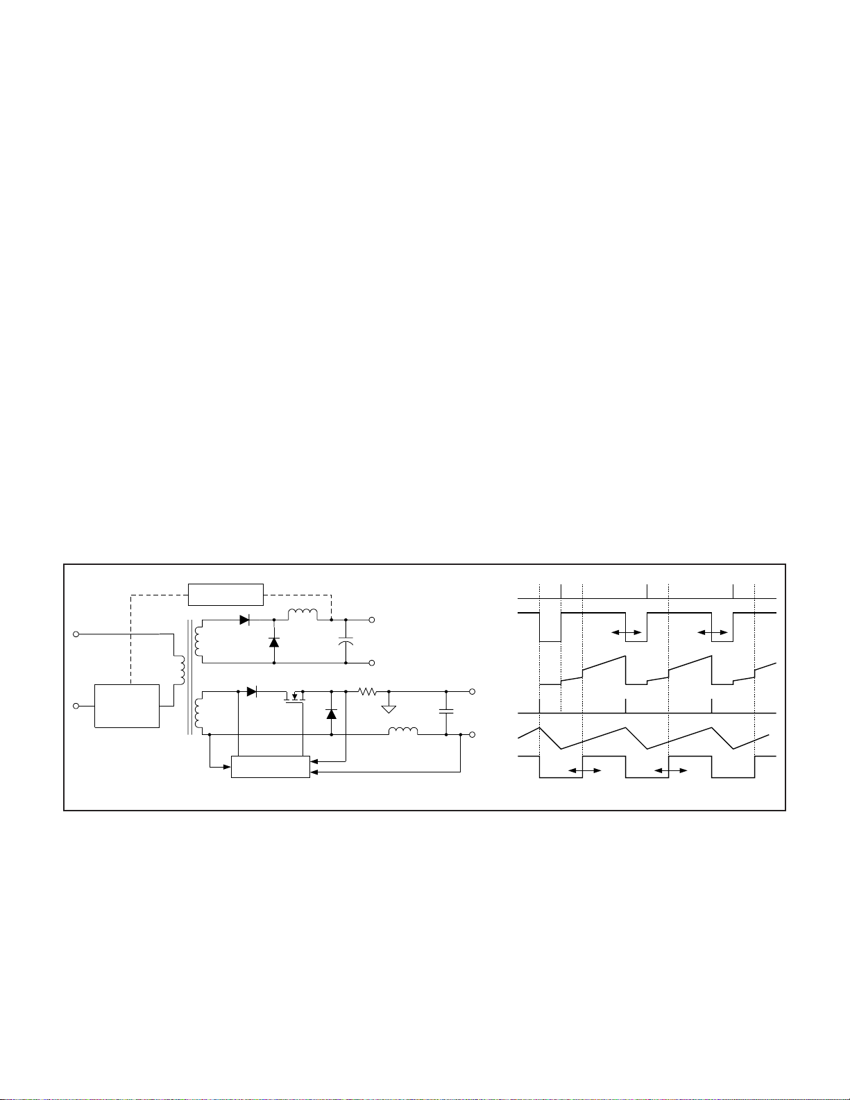
Figure 1. UCC3583 SSPR system application and typical waveforms.
PRIMARY CLOCK
PRIMARY
PULSE
PRIMARY
RAMP
CURRENT
SSPR
CLOCK
SSPR
POWER
PULSE
UDG-98195
+
O
–
6
Page 7

APPLICATION INFORMATION (cont.)
UCC1583
UCC2583
UCC3583
Note: All waveforms are referenced to chip common.
Figure 2. Single ended post regulator waveforms.
Figure 3. Half-bridge synchronous post regulator application.
7
UDG-96141-1
UDG-96142-1
Page 8

APPLICATION INFORMATION (cont.)
UCC1583
UCC2583
UCC3583
Figure 4. Half-bridge synchronous post regulator to waveforms.
8
UDG-96143-1
Page 9
APPLICATION INFORMATION (cont.)
UCC1583
UCC2583
UCC3583
Figure 5. Possible implementation for floating bias voltage generation.
-
UNI
TROD
R
B
UDG-96175-1
Figure 6. Typical application circuit.
UDG-96072-2
9
Page 10

PACKAGE OPTION ADDENDUM
www.ti.com
27-Feb-2008
PACKAGING INFORMATION
Orderable Device Status
(1)
Package
Type
Package
Drawing
Pins Package
Qty
Eco Plan
UCC2583D ACTIVE SOIC D 14 50 Green (RoHS &
no Sb/Br)
UCC2583DG4 ACTIVE SOIC D 14 50 Green (RoHS &
no Sb/Br)
UCC2583DTR ACTIVE SOIC D 14 2500 Green (RoHS &
no Sb/Br)
UCC2583DTRG4 ACTIVE SOIC D 14 2500 Green (RoHS &
no Sb/Br)
UCC2583N ACTIVE PDIP N 14 25 Green (RoHS &
no Sb/Br)
UCC2583NG4 ACTIVE PDIP N 14 25 Green (RoHS &
no Sb/Br)
UCC2583Q ACTIVE PLCC FN 20 46 Green (RoHS &
no Sb/Br)
UCC2583QG3 ACTIVE PLCC FN 20 46 Green (RoHS &
no Sb/Br)
UCC2583QTR ACTIVE PLCC FN 20 1000 Green (RoHS &
no Sb/Br)
UCC2583QTRG3 ACTIVE PLCC FN 20 1000 Green (RoHS &
no Sb/Br)
UCC3583D ACTIVE SOIC D 14 50 Green (RoHS &
no Sb/Br)
UCC3583DG4 ACTIVE SOIC D 14 50 Green (RoHS &
no Sb/Br)
UCC3583DTR ACTIVE SOIC D 14 2500 Green (RoHS &
no Sb/Br)
UCC3583DTRG4 ACTIVE SOIC D 14 2500 Green (RoHS &
no Sb/Br)
UCC3583N ACTIVE PDIP N 14 25 Green (RoHS &
no Sb/Br)
UCC3583NG4 ACTIVE PDIP N 14 25 Green (RoHS &
no Sb/Br)
(1)
The marketing status values are defined as follows:
ACTIVE: Product device recommended for new designs.
LIFEBUY: TI has announced that the device will be discontinued, and a lifetime-buy period is in effect.
NRND: Not recommended for new designs. Device is in production to support existing customers, but TI does not recommend using this part in
a new design.
PREVIEW: Device has been announced but is not in production. Samples may or may not be available.
OBSOLETE: TI has discontinued the production of the device.
(2)
Lead/Ball Finish MSL Peak Temp
CU NIPDAU Level-2-260C-1 YEAR
CU NIPDAU Level-2-260C-1 YEAR
CU NIPDAU Level-2-260C-1 YEAR
CU NIPDAU Level-2-260C-1 YEAR
CU NIPDAU N / A for Pkg Type
CU NIPDAU N / A for Pkg Type
CU SN Level-2-260C-1 YEAR
CU SN Level-2-260C-1 YEAR
CU SN Level-2-260C-1 YEAR
CU SN Level-2-260C-1 YEAR
CU NIPDAU Level-2-260C-1 YEAR
CU NIPDAU Level-2-260C-1 YEAR
CU NIPDAU Level-2-260C-1 YEAR
CU NIPDAU Level-2-260C-1 YEAR
CU NIPDAU N / A for Pkg Type
CU NIPDAU N / A for Pkg Type
(3)
(2)
Eco Plan - The planned eco-friendly classification: Pb-Free (RoHS), Pb-Free (RoHS Exempt), or Green (RoHS & no Sb/Br) - please check
http://www.ti.com/productcontent for the latest availability information and additional product content details.
TBD: The Pb-Free/Green conversion plan has not been defined.
Pb-Free (RoHS): TI's terms "Lead-Free" or "Pb-Free" mean semiconductor products that are compatible with the current RoHS requirements
for all 6 substances, including the requirement that lead not exceed 0.1% by weight in homogeneous materials. Where designed to be soldered
at high temperatures, TI Pb-Free products are suitable for use in specified lead-free processes.
Pb-Free (RoHS Exempt): This component has a RoHS exemption for either 1) lead-based flip-chip solder bumps used between the die and
package, or 2) lead-based die adhesive used between the die and leadframe. The component is otherwise considered Pb-Free (RoHS
compatible) as defined above.
Green (RoHS & no Sb/Br): TI defines "Green" to mean Pb-Free (RoHS compatible), and free of Bromine (Br) and Antimony (Sb) based flame
retardants (Br or Sb do not exceed 0.1% by weight in homogeneous material)
Addendum-Page 1
Page 11

PACKAGE OPTION ADDENDUM
www.ti.com
(3)
MSL, Peak Temp. -- The Moisture Sensitivity Level rating according to the JEDEC industry standard classifications, and peak solder
temperature.
Important Information and Disclaimer:The information provided on this page represents TI's knowledge and belief as of the date that it is
provided. TI bases its knowledge and belief on information provided by third parties, and makes no representation or warranty as to the
accuracy of such information. Efforts are underway to better integrate information from third parties. TI has taken and continues to take
reasonable steps to provide representative and accurate information but may not have conducted destructive testing or chemical analysis on
incoming materials and chemicals. TI and TI suppliers consider certain information to be proprietary, and thus CAS numbers and other limited
information may not be available for release.
In no event shall TI's liability arising out of such information exceed the total purchase price of the TI part(s) at issue in this document sold by TI
to Customer on an annual basis.
27-Feb-2008
Addendum-Page 2
Page 12

PACKAGE MATERIALS INFORMATION
www.ti.com
TAPE AND REEL INFORMATION
11-Mar-2008
*All dimensions are nominal
Device Package
UCC2583DTR SOIC D 14 2500 330.0 16.4 6.5 9.0 2.1 8.0 16.0 Q1
UCC3583DTR SOIC D 14 2500 330.0 16.4 6.5 9.0 2.1 8.0 16.0 Q1
Type
Package
Drawing
Pins SPQ Reel
Diameter
(mm)
Reel
Width
W1 (mm)
A0 (mm) B0 (mm) K0 (mm) P1
(mm)W(mm)
Pin1
Quadrant
Pack Materials-Page 1
Page 13

PACKAGE MATERIALS INFORMATION
www.ti.com
11-Mar-2008
*All dimensions are nominal
Device Package Type Package Drawing Pins SPQ Length (mm) Width (mm) Height (mm)
UCC2583DTR SOIC D 14 2500 346.0 346.0 33.0
UCC3583DTR SOIC D 14 2500 346.0 346.0 33.0
Pack Materials-Page 2
Page 14

Page 15

MECHANICAL DATA
MPLC004A – OCT OBER 1994
FN (S-PQCC-J**) PLASTIC J-LEADED CHIP CARRIER
20 PIN SHOWN
Seating Plane
0.004 (0,10)
D
D1
13
4
E1E
8
9
NO. OF
PINS
**
D/E
19
13
18
14
0.032 (0,81)
0.026 (0,66)
0.050 (1,27)
0.008 (0,20) NOM
D1/E1
MINMAXMIN
MAX
D2/E2
MIN
0.180 (4,57) MAX
0.120 (3,05)
0.090 (2,29)
0.020 (0,51) MIN
D2/E2
D2/E2
0.021 (0,53)
0.013 (0,33)
0.007 (0,18)
MAX
M
20
28
44
52
68
84
NOTES: A. All linear dimensions are in inches (millimeters).
B. This drawing is subject to change without notice.
C. Falls within JEDEC MS-018
0.385 (9,78)
0.485 (12,32)
0.685 (17,40)
0.785 (19,94)
0.985 (25,02)
1.185 (30,10)
0.395 (10,03)
0.495 (12,57)
0.695 (17,65)
0.795 (20,19)
0.995 (25,27)
1.195 (30,35)
0.350 (8,89)
0.450 (11,43)
0.650 (16,51)
0.750 (19,05)
0.950 (24,13)
1.150 (29,21)
0.356 (9,04)
0.456 (11,58)
0.656 (16,66)
0.756 (19,20)
0.958 (24,33)
1.158 (29,41)
0.141 (3,58)
0.191 (4,85)
0.291 (7,39)
0.341 (8,66)
0.441 (11,20)
0.541 (13,74)
0.169 (4,29)
0.219 (5,56)
0.319 (8,10)
0.369 (9,37)
0.469 (11,91)
0.569 (14,45)
4040005/B 03/95
POST OFFICE BOX 655303 • DALLAS, TEXAS 75265
1
Page 16
Page 17

IMPORTANT NOTICE
Texas Instruments Incorporated and its subsidiaries (TI) reserve the right to make corrections, modifications, enhancements, improvements,
and other changes to its products and services at any time and to discontinue any product or service without notice. Customers should
obtain the latest relevant information before placing orders and should verify that such information is current and complete. All products are
sold subject to TI’s terms and conditions of sale supplied at the time of order acknowledgment.
TI warrants performance of its hardware products to the specifications applicable at the time of sale in accordance with TI’s standard
warranty. Testing and other quality control techniques are used to the extent TI deems necessary to support this warranty. Except where
mandated by government requirements, testing of all parameters of each product is not necessarily performed.
TI assumes no liability for applications assistance or customer product design. Customers are responsible for their products and
applications using TI components. To minimize the risks associated with customer products and applications, customers should provide
adequate design and operating safeguards.
TI does not warrant or represent that any license, either express or implied, is granted under any TI patent right, copyright, mask work right,
or other TI intellectual property right relating to any combination, machine, or process in which TI products or services are used. Information
published by TI regarding third-party products or services does not constitute a license from TI to use such products or services or a
warranty or endorsement thereof. Use of such information may require a license from a third party under the patents or other intellectual
property of the third party, or a license from TI under the patents or other intellectual property of TI.
Reproduction of TI information in TI data books or data sheets is permissible only if reproduction is without alteration and is accompanied
by all associated warranties, conditions, limitations, and notices. Reproduction of this information with alteration is an unfair and deceptive
business practice. TI is not responsible or liable for such altered documentation. Information of third parties may be subject to additional
restrictions.
Resale of TI products or services with statements different from or beyond the parameters stated by TI for that product or service voids all
express and any implied warranties for the associated TI product or service and is an unfair and deceptive business practice. TI is not
responsible or liable for any such statements.
TI products are not authorized for use in safety-critical applications (such as life support) where a failure of the TI product would reasonably
be expected to cause severe personal injury or death, unless officers of the parties have executed an agreement specifically governing
such use. Buyers represent that they have all necessary expertise in the safety and regulatory ramifications of their applications, and
acknowledge and agree that they are solely responsible for all legal, regulatory and safety-related requirements concerning their products
and any use of TI products in such safety-critical applications, notwithstanding any applications-related information or support that may be
provided by TI. Further, Buyers must fully indemnify TI and its representatives against any damages arising out of the use of TI products in
such safety-critical applications.
TI products are neither designed nor intended for use in military/aerospace applications or environments unless the TI products are
specifically designated by TI as military-grade or "enhanced plastic." Only products designated by TI as military-grade meet military
specifications. Buyers acknowledge and agree that any such use of TI products which TI has not designated as military-grade is solely at
the Buyer's risk, and that they are solely responsible for compliance with all legal and regulatory requirements in connection with such use.
TI products are neither designed nor intended for use in automotive applications or environments unless the specific TI products are
designated by TI as compliant with ISO/TS 16949 requirements. Buyers acknowledge and agree that, if they use any non-designated
products in automotive applications, TI will not be responsible for any failure to meet such requirements.
Following are URLs where you can obtain information on other Texas Instruments products and application solutions:
Products Applications
Amplifiers amplifier.ti.com Audio www.ti.com/audio
Data Converters dataconverter.ti.com Automotive www.ti.com/automotive
DSP dsp.ti.com Broadband www.ti.com/broadband
Clocks and Timers www.ti.com/clocks Digital Control www.ti.com/digitalcontrol
Interface interface.ti.com Medical www.ti.com/medical
Logic logic.ti.com Military www.ti.com/military
Power Mgmt power.ti.com Optical Networking www.ti.com/opticalnetwork
Microcontrollers microcontroller.ti.com Security www.ti.com/security
RFID www.ti-rfid.com Telephony www.ti.com/telephony
RF/IF and ZigBee® Solutions www.ti.com/lprf Video & Imaging www.ti.com/video
Mailing Address: Texas Instruments, Post Office Box 655303, Dallas, Texas 75265
Copyright © 2008, Texas Instruments Incorporated
Wireless www.ti.com/wireless
 Loading...