

Page 1
UCB1500
PCI to AC97 bridge/host controller
Rev. 01 — 4 February 2000 Objective specification
1. General description
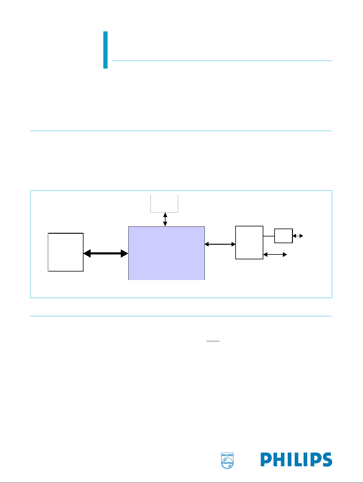
UCB1500 is a PCI-to-AC97 Bridge/Host Controller for modem or audio codecs
equipped with the AC-link interface. It integrates a PCI 2.2 compliant interface for
communication with the host PC, with built in support for PPMI (PCI Power
Management Interface) and wake-up. It also integrates an AC97 Rev. 2.1 compliant
host controller for connection to up to two AC-Link codecs, including analog modem
front ends such as the Philips UCB1510, and audio codecs.
Optional
EEPROM
c
c
PCI Interface
UCB1500
Host PC
Fig 1. Application with Philips UCB1510 analog modem front end
2. Features
■ 32-bit PCI 2.2 interface with bus master support
◆ Support up to two PCI functions with independent scatter/gather DMA
◆ PPMI and wake-up support via PME and V
◆ Download of subsystem IDs and auxiliary power consumption via optional
serial EEPROM
◆ 5 V tolerant interface for motherboard/PC add-on
■ AC97 rev 2.1 compliant host controller interface
◆ Supports up to two codecs
◆ Supports variable sample rate via the SLOTREQ protocol and valid tag bits
◆ Low latency GPIO data transfer
◆ Support modem wake-up on ring from D3cold
AC97
Interface
UCB1510
AUX
DAA
Phone
Line
GPIO
Page 2
Philips Semiconductors
UCB1500
PCI to AC97 bridge/host controller
■ Advanced power management support
◆ PPMI (PCI Power Management Interface)
◆ Instantly available PC
◆ ACPI
3. Applications
■ PCI-AC97 bridge/host controller
■ PCI modem cards
■ Host based modems
4. Ordering information
Table 1: Ordering information
Type number Package
Name Description Version
UCB1500 LQFP80 plastic low profile quad flat package, 80 leads; body 12 × 12 × 1.4 mm SOT315-1
5. Block diagram
PCI
Interface
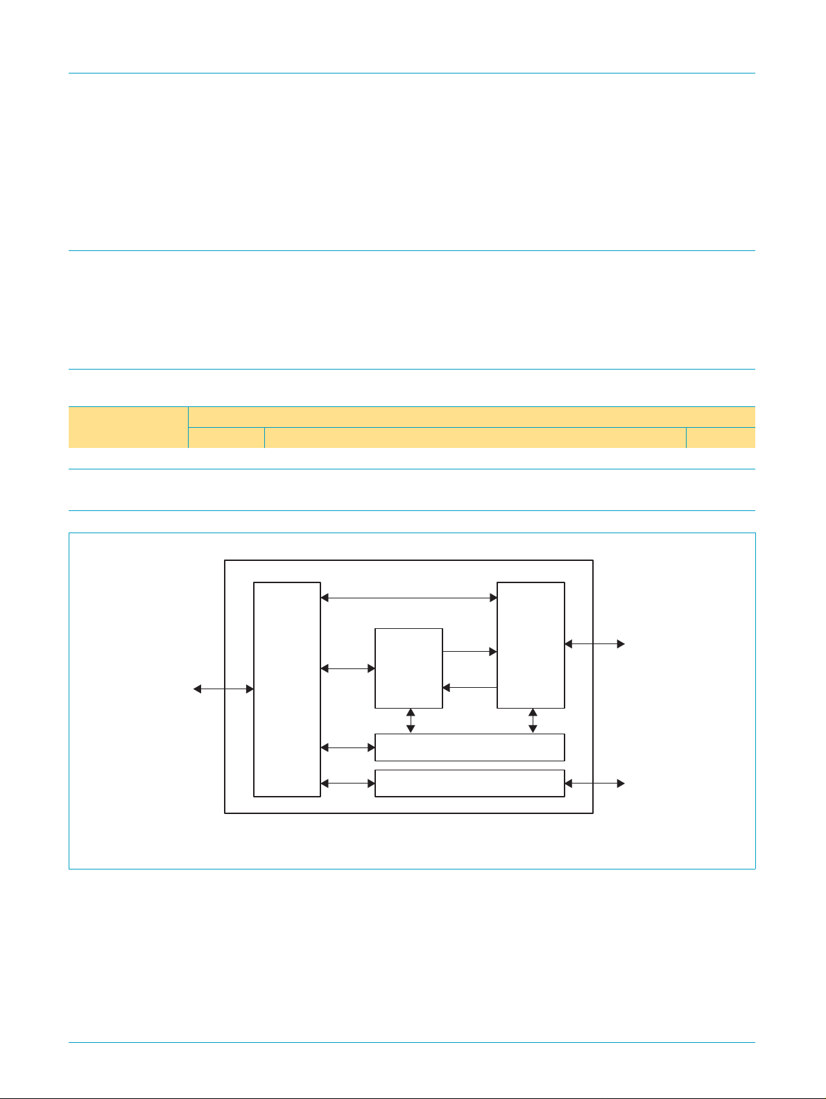
Fig 2. UCB1500 block diagram
PCI
Interface
DMA
Engine
Interrupt Control
EEPROM Interface
AC97
Controller
AC97
Interface
EEPROM
SC00177
9397 750 06854
Objective specification Rev. 01 — 4 February 2000 2 of 58
© Philips Electronics N.V. 2000. All rights reserved.
Page 3

Philips Semiconductors
6. Pinning information
6.1 Pinning
UCB1500
PCI to AC97 bridge/host controller
V
GNT
REQ
AD31
AD30
V
AD29
AD28
AD27
AD26
V
AD25
AD24
CBE3
IDSEL
V
AD23
AD22
AD21
AD20
INTA
AD18
SS
V
AD17
BITCLK
AD16
V
CLKRUN
PCICLK
TEST
78 77 76 75 74 73 72 71 7080 79 69 68 67 66 65
1
DD
2
3
4
5
6
SS
7
8
9
10
11
DD
12
13
14
15
16
SS
17
18
19
20
23 24 25 26 27 28 29
DD
VSSV
AD19
EEPD
DD
SS
V
EEPCLK
UCB1500
30 3121 22
CBE2
FRAME
VAUX_AV
SYNC
SDATAOUT
32 33 34 35 36
SS
V
IRDY
TRDY
RST
VAUX
STOP
DEVSEL
AC97_RST
SDATAIN1
64
37
PERR
SERR
PME
SDATAIN0
63 62 61
38 39 40
DD
V
PAR
AD0
CBE1
DD
V
60
59
58
57
56
55
54
53
52
51
50
49
48
47
46
45
44
43
42
41
SS
V
SC00178
AD1
AD2
V
SS
AD3
AD4
AD5
AD6
V
DD
AD7
CBE0
AD8
AD9
V
SS
AD10
AD11
AD12
AD13
V
DD
AD14
AD15
Fig 3. Pin configuration
6.2 Pin description
Table 2: Pin description
Symbol Pin Type Description
PCI interface
PCICLK 80 I PCI system clock.
RST 68 I PCI system reset, V
REQ 3 T/S PCI bus request.
GNT 2 T/S PCI bus grant.
FRAME 29 S/T/S
9397 750 06854
Objective specification Rev. 01 — 4 February 2000 3 of 58
[1]
PCI FRAME, input during slave, output during master.
powered.
AUX
© Philips Electronics N.V. 2000. All rights reserved.
Page 4

Philips Semiconductors
UCB1500
PCI to AC97 bridge/host controller
Table 2: Pin description
…continued
Symbol Pin Type Description
IRDY 30 S/T/S PCI IRDY, input during slave, output during master.
TRDY 31 S/T/S PCI TRDY, output during slave, input during master.
DEVSEL 33 S/T/S PCI DEVSEL, output during slave, input during master.
STOP 34 S/T/S PCI STOP, output during slave, input during master.
IDSEL 15 I PCI IDSEL signal.
AD[31:0] 4, 5, 7, 8, 9, 10, 12,
13, 17, 18, 19, 20,
23, 24, 25, 26,41,
42, 44, 45, 46, 47,
T/S PCI address/data.
slave mode: output only during data read phase.
master mode: output during address phase and data write phase.
49, 50, 52, 54, 55,
56, 57, 59, 60, 62
CBE[3:0] 14, 28, 39, 51 T/S PCI command/byte-enable, input during slave, output during master.
PAR 38 T/S PCI parity.
INTA 77 O/D
PME 63 O/D Open drain, V
[2]
PCI interrupt.
pins are V
powered PCI power management pin. SDA TAIN[1:0]
AUX
powered and can trigger PME.
AUX
SERR 36 O/D PCI system error
PERR 35 S/T/S PCI parity error
CLKRUN 78 S/T/S Primary PCI bus clock run. Used by the central resource to stop the PCI
clock or to slow it down
AC link controller interface
BITCLK 75 I Serial data clock; or input for secondary codecs.
SDATAIN[1:0] 65. 64 I Input from AC97/MC97 codecs. V
SDATAOUT 70 O Output to AC97/MC97 codecs. Driven to 0 at power-up or when
powered and can trigger PME.
AUX
RST
asserted.
SYNC 71 O AC97 sync. Driven to 0 at power-up or when
AC97_RST 66 O AC97 reset. Driven to 0 at power-up or when RST asserted. V
RST asserted.
AUX
powered.
Serial EEPROM interface
EEPCLK 73 O EEPROM clock.
EEPD 74 I/O EEPROM serial data port.
Power management; miscellaneous
_AV 69 I Auxiliary power available, V
V
AUX
powered.
AUX
TEST 79 I Test mode.
Power pins
V
DD
1, 11, 22, 27, 37,
S 3.3 V power pins.
43, 53, 61
V
SS
6, 16, 21, 32, 40,
S Ground pins.
48, 58, 72, 76
V
AUX
67 S Auxiliary power. If auxiliary power is not available or not necessary, this pin
must be connected to V
DD
.
[1] S/T/S: Sustained Tri-State is an active-LOW tri-state signal owned anddriven by one agent at a time. The agent that drives an S/T/S pin
LOW must drive it HIGH for at least one clock before letting it float. A new agent cannot start driving a S/T/S signal any sooner than one
clock after the previous owner tri-states it.
[2] O/D: Open Drain allows multiple devices to share as a wired OR.
9397 750 06854
Objective specification Rev. 01 — 4 February 2000 4 of 58
© Philips Electronics N.V. 2000. All rights reserved.
Page 5

Philips Semiconductors
7. PCI configuration space
7.1 Overview
By default, UCB1500 supports a single modem function. Under control of BIOS or an
external serial EEPROM, UCB1500 can support a maximum of two PCI functions,
which are typically one modem plus one audio functions. To allow IHV to overwrite
parameters such as Device ID, Vendor ID, Subsystem Vendor ID, Subsystem ID,
Class Code and Power Management Capabilities, UCB1500 provides two schemes:
For each function, Device ID, Vendor ID, Subsystem Vendor ID, Subsystem ID,
•
Class Code and Power Management Capabilities are placed in a dedicated PCI
configuration read/write area accessible by the corresponding function. An enable
bit for Function 1 is placed in a dedicated read/write area accessible byFunction 0.
This allows IHVs to enable Function 1 and change the corresponding read-only
parameters of Functions 0 and 1 (if enabled) in the BIOS POST routine when
UCB1500 is used as a motherboard device.
In case UCB1500 is used as a PCI card which BIOS cannot control, the above
•
parameters, together with Function 1 enable, can be changed by the external
serial EEPROM.
UCB1500
PCI to AC97 bridge/host controller
The EEPROM data map is given in Table 3.
Table 3: EEPROM data map
Byte address Tag Description
00-01h signature 1516h = valid signature, otherwise disable autoloading.
02-03h control Bit 0: 1=enable function 1, 0=disable function 1
Bit 1: 1=enable function 0 auto-loading from address 04-9Dh
Bit 2: 1=enable function 0 auto-loading from address 0A-11h
Bit 3: 1=enable function 1 auto-loading from address 10-17h
Bit 4: 1=enable function 1 auto-loading from address 18-1Fh
Other bits: reserved and must be 0s.
04-05h sub_vendorID Function 0 subsystem vendor ID, PCI configuration space address 2C-2Dh.
06-07h subsystemID Function 0 subsystem ID, PCI configuration space address 2E-2Fh.
08-09h pmc Function 0 power management capabilities, PCI configuration space address 82h.
0A-0Bh vendorID Function 0 vendor ID, PCI configuration space address 00-01h.
0C-0Dh deviceID Function 0 device ID, PCI configuration space address 02-03h.
0Eh -- Reserved.
0F-11h classCode Function 0 Class Code, PCI configuration space address 09-0Bh.
12-13h sub_vendorID Function 1 subsystem vendor ID, PCI configuration space address 2C-2Dh.
14-15h subsystemID Function 1 subsystem ID, PCI configuration space address 2E-2Fh.
16-17h pmc Function 1 power management capabilities, PCI configuration space offset 82h.
18-19h vendorID Function 1 vendor ID, PCI configuration space address 00-01h.
1A-1Bh deviceID Function 1 device ID, PCI configuration space address 02-03h.
1Ch -- Reserved.
1D-1Fh classCode Function 1 Class Code, PCI configuration space address 09-0Bh.
9397 750 06854
Objective specification Rev. 01 — 4 February 2000 5 of 58
© Philips Electronics N.V. 2000. All rights reserved.
Page 6

Philips Semiconductors
UCB1500
PCI to AC97 bridge/host controller
7.2 Configuration registers
7.2.1 Function 0 configuration registers
UCB1500 supports the PCI configuration cycle to control the UCB1500 access. It
sets up the PCI configuration bits and the UCB1500 IO port address. The following
table shows the supported PCI registers and their default values. Some of the
registers are programmable through the EEPROM interface (See EEPROM section
for details).
Remark: All registers are read/write, unless specified otherwise. Shaded registers
are read-only. A register with (S) means it is powered by V
sticky or otherwise stated, all read/write registers defaults to zero at PCI reset. All
reserved or unimplemented registers are hardwired to 0.
Table 4: Function 0 configuration registers
31-24 23-16 15-8 7-0 Address
Device ID = 3400
Modified by BIOS via writing to 42h or EEPROM auto
loading
Status = 0290 Command = 0000 04h
Class Code = 070300
Simple communication controller, generic modem.
Modified by BIOS via writing to 45h or EEPROM auto loading.
BIST = 00 Header Type
If multifunction,
header type = 80h,
otherwise 00h
I/O port Base Address [31:16]
Hardwired to 0000h
Reserved. 14h-2Bh
Subsystem ID = 3400
Modified by BIOS via writing to 6Eh or EEPROM auto
loading
Reserved 30h
Reserved
Reserved 38h
Reserved
Device ID Write = 3400 Vendor ID Write = 1131 40h
Class Code Write = 070300
Reserved EEPROM Status =00 48h
Reserved 4C-4Fh
Reserved
Reserved 54-67h
PMC Write = C801 Reserved 68h
Vendor ID = 1131
Modified by BIOS via writing to 40h or EEPROM auto
loading
Revision ID = 01 08h
Latency Timer = 00 Cache Line Size = 00 0Ch
I/O port Base Address[15:0] = 0001 10h
Subsystem Vendor ID = 1131
Modified by BIOS via writing to 6Ch or EEPROM auto
loading
Capability Pointer = 80 34h
Interrupt Pin = 01 Interrupt Line = 00 3Ch
Revision ID = 01 44h
Test Register = 00 50
and is sticky. Unless
AUX
00h
2Ch
9397 750 06854
Objective specification Rev. 01 — 4 February 2000 6 of 58
© Philips Electronics N.V. 2000. All rights reserved.
Page 7

Philips Semiconductors
UCB1500
PCI to AC97 bridge/host controller
Table 4: Function 0 configuration registers
31-24 23-16 15-8 7-0 Address
Subsystem ID Write = 3400 Subsystem Vendor ID Write = 1131 6Ch
Reserved 70-7Fh
PMC =
4801 (V
C801 (V
Modified by BIOS via writing to 6Ah, or EEPROM
autoloading to PCI-PM1.1
Reserved PMCSR = 0000 (S) 84h
= 0, no autoload)
AUX_AV
= 1, no autoload)
AUX_AV
…continued
Next Item Per = 00 Capability ID = 01 80h
[01-00]: Vendor ID (read only): Programmable through EEPROM interface, or
register 40h. Default value = 1131h
[03-02]: Device ID (read only): Programmable through EEPROM interface, or
register 42h. Default value = 3400h
[05-04]: Command Register
Table 5: Command Register bit description
Bit Description
15-10 Reserved.
9(r) Fast Back-to-back Transactions
Always 0, fast back-to-back transactions is not supported.
8
7(r) Address/Data Stepping
6 Parity Error Response
5(r) VGA Snooping
4(r) Memory Write and Invalidate Command
3(r) Special Cycle Response
2 Bus Master Control
1(r) Memory Space Response
0 I/O Space Control
SERR enable
If set,
SERR driver is enabled; if 0, SERR is disabled.
Always 0, address/data stepping is not implemented.
When set, the device must take its normal action when a parity error is detected.
If this bit is 0, the devicemust ignore any parity errors that it detects and continue
normal operation.
Always 0, not implemented.
Always 0, UCB1500 does not generate memory write and invalidate command.
Always 0, UCB1500 ignores all special cycles.
PCI Master access enable; this bit must be enabled to activate UCB1500 DMA
register.
1 = enable.
Always 0, UCB1500 does not respond to memory space accesses.
UCB1500 control register I/O space access enable.
1 = enable.
9397 750 06854
Objective specification Rev. 01 — 4 February 2000 7 of 58
© Philips Electronics N.V. 2000. All rights reserved.
Page 8

Philips Semiconductors
[07-06]: Status Register
Table 6: Status Register bit description
Bit Description
15
14
13 Received master abort
12 Received target abort
11(r) Target abort
10-9(r) Timing
8
7(r) Fast back-to-back capable
6(r) User Definable features
5(r) 66 MHz capable bit
4(r) Capabilities bit (read only)
3-0 Reserved.
UCB1500
PCI to AC97 bridge/host controller
PERR detected
Set to ‘1’ whenever parity error is detected. Write ‘1’ to clear.
SERR asserted
Set to ‘1’ if UCB1500 asserted
If set, UCB1500 has received master abort during its slaveoperation. Write ‘1’ to
clear.
If set, UCB1500 has received target abort during its master operation. Write `1'
to clear
Always ‘0’; UCB1500 never signals target abort.
Always 01b; wait state during slave access to UCB1500.
PERR reported
Not implemented, always 0.
Always ‘1’; NO wait state between PCI cycles.
Always ‘0’; device does not support user definable features.
Always ‘0’; device is 33MHz device only.
Always ‘1’; capabilities present.
SERR. Write ‘1' to clear.
[08]: Revision ID (read only): Current revision of chip = 1.
[0B-09]: Class Code Register (read only): Value = 070300h for simple
communication controller, generic modem. Programmable through EEPROM
interface or register 47-45h.
[0C]: Cache Line Size (read only): Always 0; no cache supported.
[0D]: Latency Timer
Table 7: Latency Timer register bit description
Bit Description
7-4 Latency Timer
Bits 7-4 of the latency timer, in units of PCI clocks * 16.
3-0(r) Latency Timer
These bits are read only and are always0000b, giving timer granularity of 16 PCI
clocks.
[0E]: Header Type (read only): If multifunction device, value is 80h otherwise 00h.
9397 750 06854
Objective specification Rev. 01 — 4 February 2000 8 of 58
© Philips Electronics N.V. 2000. All rights reserved.
Page 9

Philips Semiconductors
[0F]: BIST (read only): Always 0; no built-in test capability.
[10]: I/O port base address
Table 8: I/O Port Base Address register bit description
Bit Description
31-16(r) I/O port Base address
15-4 I/O port Base address
3-1 Always 000b
0 Always 1b
[2C-2F] Subsystem ID/Subsystem Vendor ID (read only): Programmable through
EEPROM interface or through register 6e-6ch. Default Value = 3400h/1131h.
[34] Capability pointer (read only): 80h points to start offset of power management
registers.
[3C]: Interrupt Register
UCB1500
PCI to AC97 bridge/host controller
A[31:16] always 0.
A[15:4]; programmable address space for control registers.
Table 9: Interrupt Register bit description
Bit Description
15:8 Interrupt pin (read only)
Always 01h; interrupt pin connected to
7:0 Interrupt line
Interrupt line routing information.
INTA.
[40-43] Device ID Write / Vendor ID Write: This register contains a copy of the
Device ID and Vendor ID registers. Writing to this register will update the original
Device ID and Vendor ID registers (offset 0h - 3h).
[44h]: Revision ID: Same as offset 08h.
[45-47] Class code Write: This register contains a copy of the Class Code registers.
Writing to this register will update the original Class Code registers (offset 9h-Bh).
[48]: EEPROM status register /Misc
Table 10: EEPROM Status register bit description
Bit Description
0 EEPROM autoload status
If set, EEPROM autoload cycle is in progress.
9397 750 06854
Objective specification Rev. 01 — 4 February 2000 9 of 58
© Philips Electronics N.V. 2000. All rights reserved.
Page 10

Philips Semiconductors
[50]: Test Register (For internal use only)
Table 11: Test Register bit description
Bit Description
0 Test Mode Enable
1 EEPROM Autoload enable
[6A-6B]: Power Management capabilities Write: This register contains a copy of
the Power Management capabilities register. Writing to this register will update the
original Power Management capabilities register (offset 82h-83h).
[6C-6F]: Subsystem-ID Write / Vendor ID Write: This register contains a copy of
the Subsystem-ID/Vendor ID register. Writing to this register will update the original
Subsystem-ID/Vendor ID registers (offset 2Ch-2Fh).
[80]: Capability Identifier (read only): This register is set to 01h to indicate power
management interface registers.
UCB1500
PCI to AC97 bridge/host controller
If set, chip operates under test mode. If ‘0’, chip operates normally.
If set, EEPROM autoload is disabled. If `0', EEPROM autoload sequence
operates as normal, depending on the EEPROM signature. This bit is for testing
only.
[81]: Next Item Pointer (read only): This field provides an offset into the function's
PCI Configuration Space pointing to the location of next item in the function's
capability list. This register is set to zero, signifying that there are no additional items
in the capability list.
9397 750 06854
Objective specification Rev. 01 — 4 February 2000 10 of 58
© Philips Electronics N.V. 2000. All rights reserved.
Page 11

Philips Semiconductors
[82]: Power Management Capabilities (read only)
Table 12: Power Management Capabilities register bit description
Read only
Bit Description
15-11(r) PME support
10(r) D2 support
9(r) D1 support
8-6(r) Aux_Current
5(r) DSI
4(r) Reserved.
3(r) PME Clock
2:0(r) Version
UCB1500
PCI to AC97 bridge/host controller
This 5-bit field indicates the power states in which the function may assert
Value is set to 11001 b if V
D3cold and D0. If V
AUX_AV
= 1 to indicate PME can be asserted from
AUX_AV
= 0, this field is set to 01001b to indicate PME can be
asserted from D3hot and D0.
The entire setting can be overwritten by BIOS via writing to 6Ah, or an external
EEPROM. If V
= 0, bit 15 shall always be zero. If V
AUX_AV
= 1, bit 15 shall
AUX
reflect the setting of 6Ah, or that loaded from EEPROM.
This bit is set to ‘0’ to indicate that function does not support the D2 power
management state. This setting can be overwritten by BIOS via 6Ah, or with the
external EEPROM.
This bit is set to ‘0’ to indicate that function does not support the D1 power
management state. This setting can be overwritten by BIOS via 6Ah, or with the
external EEPROM.
These bits are set to ‘0’ for PCI-PM 1.0 compliance. For PCI-PM 1.1 compliance,
these bits are overwritten by BIOS via 6Ah, or loaded from an external EEPROM
to reflect the 3.3V
current requirement.
AUX
The Device Specific Initialization bit indicates whether special initialization of this
function is required (beyond the standard PCI configuration header) before the
generic class device driver is able to use it. This register is set to ‘0’ to indicate
that it does not require special initialization.
This bit is a ‘0’, indicating that the function does not rely on the presence of the
PCI clock for
PME operation.
This register is set to 001b, indicating that this function complies with Rev 1.0 of
PCI Power Management Interface Specification
the
. These bits can also be
overwritten by BIOS via 6Ah, or loaded from an external EEPROM to 010b for
compliance with PCI-PM 1.1.
PME.
9397 750 06854
Objective specification Rev. 01 — 4 February 2000 11 of 58
© Philips Electronics N.V. 2000. All rights reserved.
Page 12

Philips Semiconductors
UCB1500
PCI to AC97 bridge/host controller
[84]: Power Management Control/Status: (V
powered: Only PME Status and
AUX
PME_EN are sticky.)
Table 13: Power Management Control/Status register bit description
Bit Description
15 PME Status - Sticky Bit
This bit is set when the function would normally assert the
independent of the state of the PME_EN bit. This bit is set when a power
management event occurs.
Writing a ‘1’ to this bit will clear it and cause the function to stop asserting a
(if enabled). Writing a ‘0’ has no effect.
14-13(r) Data scale
Not implemented.
12-9 Data select
This 4-bit field is used to select which data is to be reported through the Data
register and Data scale field. This function is not implemented in this chip.
8 PME_EN - Sticky Bit
A ‘1’ enables the function to assert
7-2(r) Reserved.
1-0 Power State
This 2-bit field is used both to determine the current power state of a function
and to set the function into a new power state. The definition of the field values is
given below.
00b - D0
01b - D1
10b - D2
11b - D3hot
If software writes D1 or D2 and the corresponding bit 10 or 9 or register 82
indicates it is not supported, the state change is discarded.
PME. When ‘0’, PME assertion is disabled.
PME signal
PME
[86-87]: Reserved.
9397 750 06854
Objective specification Rev. 01 — 4 February 2000 12 of 58
© Philips Electronics N.V. 2000. All rights reserved.
Page 13

Philips Semiconductors
UCB1500
PCI to AC97 bridge/host controller
7.2.2 Function 1 Configuration Registers
Table 14: Function 1 configuration registers
31-24 23-16 15-8 7-0 Address
Device ID = 3401
Modified by BIOS via writing to 42h or
EEPROM auto loading
Status = 0290 Command = 0000 04h
Class Code = 040100
Multimedia Audio Device.
Modified by BIOS via writing to 45h or EEPROM auto loading.
BIST = 00 Header Type = 00 Latency Timer = 00 Cache Line Size = 00 0Ch
I/O port Base Address [31:16]
Hardwired to 0000h
Reserved. 14h-2Bh
Subsystem ID = 3401
Modified by BIOS via writing to 6Eh or
EEPROM auto loading
Reserved 30h
Reserved 38h
Reserved
Device ID Write = 3401 Vendor ID Write = 1131 40h
Class Code Write = 040100
Reserved EEPROM Status =00 48h
Reserved 4C-4Fh
Reserved Test Register* = 00 50
Reserved 54-67h
PMC Write = 0401 Reserved 68h
Subsystem ID Write = 3401 Subsystem Vendor ID Write = 1131 6Ch
Reserved 70-7fh
PMC = 0401
Modified by BIOS via writing to 6Ah, or
EEPROM autoloading to PCI-PM1.1
Reserved PMCSR = 0000 (S) 84h
Vendor ID = 1131
Modified by BIOS via writing to 40h or
EEPROM auto loading
Revision ID = 01 08h
I/O port Base Address[15:0] = 0001 10h
Subsystem Vendor ID = 1131
Modified by BIOS via writing to 6Ch or
EEPROM auto loading
Capability Pointer = 80 34h
Interrupt Pin = 01 Interrupt Line = 00 3Ch
Revision ID = 01 44h
Next Item Ptr = 00 Capability ID = 01 80h
00h
2Ch
[01-00]: Vendor ID (read only): Programmable through EEPROM interface, or
register 40h. Default value = 1131h
[03-02]: Device ID (read only): Programmable through EEPROM interface, or
register 42h. Default value = 3401h
9397 750 06854
Objective specification Rev. 01 — 4 February 2000 13 of 58
© Philips Electronics N.V. 2000. All rights reserved.
Page 14

Philips Semiconductors
[05-04]: Command Register
Table 15: Command Register bit description
Bit Description
15-10 Reserved.
9(r) Fast Back-to-back Transactions
8
7(r) Address/Data Stepping
6 Parity Error Response
5(r) VGA Snooping
4(r) Memory Write and Invalidate Command
3(r) Special Cycle Response
2 Bus Master Control
1(r) Memory Space Response
0 I/O Space Control
UCB1500
PCI to AC97 bridge/host controller
Always 0, fast back-to-back transactions is not supported.
SERR enable
If set,
SERR driver is enabled; if 0, SERR is disabled.
Always 0, address/data stepping is not implemented.
When set, the device must take its normal action when a parity error is detected.
If this bit is 0, the devicemust ignore any parity errors that it detects and continue
normal operation.
Always 0, not implemented.
Always 0, UCB1500 does not generate memory write and invalidate command.
Always 0, UCB1500 ignores all special cycles.
PCI Master access enable; this bit must be enabled to activate UCB1500 DMA
register.
1 = enable.
Always 0, UCB1500 does not respond to memory space accesses.
UCB1500 control register I/O space access enable.
1 = enable.
9397 750 06854
Objective specification Rev. 01 — 4 February 2000 14 of 58
© Philips Electronics N.V. 2000. All rights reserved.
Page 15

Philips Semiconductors
[07-06]: Status Register
Table 16: Status Register bit description
Bit Description
15
14
13 Received master abort
12 Received target abort
11(r) Target abort
10-9(r) Timing
8
7(r) Fast back-to-back capable
6(r) User Definable features
5(r) 66 MHz capable bit
4(r) Capabilities bit (read only)
3-0 Reserved.
UCB1500
PCI to AC97 bridge/host controller
PERR detected
Set to ‘1’ whenever parity error is detected. Write ‘1’ to clear.
SERR asserted
Set to ‘1’ if UCB1500 asserted
If set, UCB1500 has received master abort during its slaveoperation. Write ‘1’ to
clear.
If set, UCB1500 has received target abort during its master operation. Write `1'
to clear
Always ‘0’; UCB1500 never signals target abort.
Always 01b; wait state during slave access to UCB1500.
PERR reported
Not implemented, always 0.
Always ‘1’; NO wait state between PCI cycles.
Always ‘0’; device does not support user definable features.
Always ‘0’; device is 33MHz device only.
Always ‘1’; capabilities present.
SERR. Write ‘1' to clear.
[08]: Revision ID (read only): Current revision of chip = 1.
[0B-09]: Class Code Register (read only): Value = 040100h for multimedia device,
audio. Programmable through EEPROM interface or register 47-45h.
[0C]: Cache Line Size (read only): Always 0; no cache supported.
[0D]: Latency Timer
Table 17: Latency Timer register bit description
Bit Description
7-4 Latency Timer
Bits 7-4 of the latency timer, in units of PCI clocks * 16.
3-0(r) Latency Timer
Bits 3-0 of the latency timer. These bits are read only and are always 0000b,
giving timer granularity of 16 PCI clocks.
[0E]: Header Type (read only): Always 0.
9397 750 06854
Objective specification Rev. 01 — 4 February 2000 15 of 58
© Philips Electronics N.V. 2000. All rights reserved.
Page 16

Philips Semiconductors
[0F]: BIST (read only): Always 0; no built-in test capability.
[10]: I/O port base address
Table 18: I/O Port Base Address register bit description
Bit Description
31-16(r) I/O port Base address
15-4 I/O port Base address
3-1 Always 000b
0 Always 1b
[2C-2F] Subsystem ID/Subsystem Vendor ID (read only): Programmable through
EEPROM interface or through register 6E-6Ch. Default Value = 3401h / 1131h.
[34] Capability pointer (read only): 80h points to start offset of power management
registers.
[3C]: Interrupt Register
UCB1500
PCI to AC97 bridge/host controller
A[31:16] always 0.
A[15:4]; programmable address space for control registers.
Table 19: Interrupt Register register bit description
Bit Description
15:8 Interrupt pin (read only)
Always 01h interrupt pin connected to
7:0 Interrupt line
Interrupt line routing information.
INTA.
[40-43] Device ID Write / Vendor ID Write: This register contains a copy of the
Device ID and Vendor ID registers. Writing to this register will update the original
Device ID and Vendor ID registers (offset 0h-3h).
[44h]: Revision ID: Same as offset 08.
[45-47] Class code Write: This register contains a copy of the Class Code registers.
Writing to this register will update the original Class Code registers (offset 9h-Bh).
[48]: EEPROM status register /Misc
Table 20: EEPROM Status Register / Misc. register bit description
Bit Description
0 EEPROM autoload status
If set, EEPROM autoload cycle is in progress.
9397 750 06854
Objective specification Rev. 01 — 4 February 2000 16 of 58
© Philips Electronics N.V. 2000. All rights reserved.
Page 17

Philips Semiconductors
[50]: Test Register (For internal use only)
Table 21: Test Register register bit description
Bit Description
0 Test Mode Enable
1 EEPROM Autoload Enable
[6A-6B]: Power Management capabilities Write: This register contains a copy of
the Power Management capabilities register. Writing to this register will update the
original Power Management capabilities register (offset 82h-83h).
[6C-6F]: Subsystem-ID Write / Vendor ID Write: This register contains a copy of
the Subsystem-ID/Vendor ID register. Writing to this register will update the original
Subsystem-ID/Vendor ID registers (offset 2Ch-2Fh).
[80]:Capability Identifier (read only): This register is set to 01h to indicate power
management interface registers.
UCB1500
PCI to AC97 bridge/host controller
If set, chip operates under test mode. If ‘0’, chip operates normally.
If set, EEPROM autoload is disabled. If ‘0’, EEPROM autoload sequence
operates as normal, depending on the EEPROM signature. This bit is for testing
only.
[81]: Next Item Pointer (read only): This field provides an offset into the function's
PCI Configuration Space pointing to the location of next item in the function's
capability list. This register is set to zero, signifying that there are no additional items
in the capability list.
9397 750 06854
Objective specification Rev. 01 — 4 February 2000 17 of 58
© Philips Electronics N.V. 2000. All rights reserved.
Page 18

Philips Semiconductors
[82]: Power Management Capabilities (read only)
Table 22: Power Management Capabilities register bit description
Read only
Bit Description
15-11(r) PME support
10(r) D2 support
9(r) D1 support
8-6(r) Aux_Current
5(r) DSI
4(r) Reserved.
3(r) PME Clock
2:0(r) Version
UCB1500
PCI to AC97 bridge/host controller
This 5-bit field indicates the power states in which the function may assert
Value is set to 00000b to indicate no
The entire setting can be overwritten by BIOS via writing to 6Ah, or an external
EEPROM. If V
reflect the setting of 6Ah, or that loaded from EEPROM.
This bit is set to ‘1’ to indicate that function supports the D2 power management
state. This setting can be overwritten by BIOS via 6Ah, or with the external
EEPROM.
This bit is set to ‘0’ to indicate that function does not support the D1 power
management state. This setting can be overwritten by BIOS via 6Ah, or with the
external EEPROM.
These bits are set to ‘0’ for PCI-PM 1.0 compliance. For PCI-PM 1.1 compliance,
these bits are overwritten by BIOS via 6Ah, or loaded from an external EEPROM
to reflect the 3.3V
The Device Specific Initialization bit indicates whether special initialization of this
function is required (beyond the standard PCI configuration header) before the
generic class device driver is able to use it. This register is set to ‘0’ to indicate
that it does not require special initialization.
This bit is a ‘0’, indicating that the function does not rely on the presence of the
PCI clock for
This register is set to 001b, indicating that this function complies with Rev 1.0 of
PCI Power Management Interface Specification
the
overwritten by BIOS via 6Ah, or loaded from an external EEPROM to 010b for
compliance with PCI-PM 1.1.
PME operation.
= 0, bit 15 shall always be zero. If V
AUX_AV
current requirement.
AUX
PME can be asserted.
AUX
. These bits can also be
= 1, bit 15 shall
PME.
9397 750 06854
Objective specification Rev. 01 — 4 February 2000 18 of 58
© Philips Electronics N.V. 2000. All rights reserved.
Page 19

Philips Semiconductors
UCB1500
PCI to AC97 bridge/host controller
[84]: Power Management Control/Status (V
Table 23: Power Management Control/Status register bit description
V
powered.
AUX
Bit Description
15 PME Status - Sticky Bit
This bit is set when the function would normally assert the
independent of the state of the PME_EN bit. This bit is set when a power
management event occurs.
Writing a ‘1’ to this bit will clear it and cause the function to stop asserting a
(if enabled). Writing a ‘0’ has no effect.
14-13(r) Data scale
Not implemented.
12-9 Data select
This 4-bit field is used to select which data is to be reported through the Data
register and Data scale field. This function is not implemented in this chip.
8 PME_EN - Sticky Bit
A ‘1’ enables the function to assert
7-2(r) Reserved.
1-0 Power State
This 2-bit field is used both to determine the current power state of a function
and to set the function into a new power state. The definition of the field values is
given below.
00b - D0
01b - D1
10b - D2
11b - D3hot
If software writes D1 or D2 and the corresponding bit 10 or 9 or register 82
indicates it is not supported, the state change is discarded.
powered)
AUX
PME. When ‘0’, PME assertion is disabled.
PME signal
PME
[86-87]: Reserved
9397 750 06854
Objective specification Rev. 01 — 4 February 2000 19 of 58
© Philips Electronics N.V. 2000. All rights reserved.
Page 20

Philips Semiconductors
8. Control Registers
To access any of the registers listed below, HOST needs to:
I/O write 8-bit data to the index port.
•
Read 8/16 bits from data port or write 8/16 bits to data port.
•
Data and Index Port Addresses are as follows:
Data Port = base address + 0h
•
Index Port = base address + 2h
•
All registers bits default to a value of 0 at power-up, unless otherwise stated. Sticky
bits initially haveunknown values at power-up, and retain programmed values if V
is available.
In addition to the Data port and the Index port, there are also status ports 1 and 2.
These ports can be used for interrupt handling. See section on interrupts for details.
The status port addresses are as follows:
UCB1500
PCI to AC97 bridge/host controller
AUX
Status port1 = base address + 4h (DMA status)
•
Status port2 = base address + ch (AC97 status)
•
Remark: Base address is specified in register 10h of the PCI configuration space. All
registers are word-based, accessible by HOST. All registers are read/write registers,
unless specified otherwise by the following notation: (r) = read only, (w) = write only.
Unless sticky or otherwise stated, all read/write registers default to zero at PCI reset.
All reserved or unimplemented registers are hardwired to 0.
Function 0 and Function 1 registers can be accessed through the specified I/O base
address programmed into register 10h. Even though function 0 and function 1 can
access the registers through different I/O addresses, there is only one physical set of
control registers for both functions. As a result of this, if function 0 writes to register 0
for example, followed by function 1 write to register 0, then if function 0 reads
register 0, it will get the value written by function 1.
8.1 DMA Registers
8.1.1 [0000-000F] Reserved.
8.1.2 [0010]: Receive DMA #1 Descriptor Table Pointer (DTP) register
Table 24: Receive DMA #1 DPT register bit description
Bit Description
15-3 Descriptor Table Pointer [15:3]
Bits 15-3 of receive DMA #1 Descriptor Table Pointer. 32-bit DTP points to
location of descriptor table in local memory.
9397 750 06854
Objective specification Rev. 01 — 4 February 2000 20 of 58
© Philips Electronics N.V. 2000. All rights reserved.
Page 21

Philips Semiconductors
8.1.3 [0011]: Receive DMA #1 Descriptor table pointer (DTP) register
Table 25: Receive DMA #1 DPT register bit description
Bit Description
15-0 Descriptor Table Pointer [31:16]
8.1.4 [0012]: Receive DMA #1 FIFO count register
Table 26: Receive DMA #1 FIFO count register bit description
Bit Description
15(r) Open PCI Master Cycle
14 DTP Invalid Bit Mask
13-7 Reserved.
6-0(r) Receive DMA #1 FIFO count
UCB1500
PCI to AC97 bridge/host controller
Bits 31-16 of receive DMA #1 Descriptor Table Pointer.
(For internal use only): This bit is set if there is an outstanding PCI master cycle
as a result of PCI retry termination by the target. Software should wait for this bit
to be cleared when initiating another DMA transfer right after an aborted DMA
transfer.
If this bit is set to ‘1’, the receive DMA engine will not stop even if the current
descriptor fetched has the invalid bit set.
(Forinternal use only) number of receivedbytes that is still in the internal 64-byte
FIFO.
8.1.5 [0013]: Receive DMA #1 command register
Table 27: Receive DMA #1 Command Register bit description
Bit Description
15-14 Threshold level
Specifies the level at which data is transferred from the 64-byte FIFO to main
memory. Recommended setting is for at least 16 bytes threshold.
00 = 4 bytes, data will be transferred to memory as soon as there is at least
4 bytes of receive data in the receive FIFO
01 = 16 bytes
10 = 32 bytes
11 = 48 bytes
13 Buffer Overrun auto recovery (for internal user only)
If set, UCB1500 will automatically recover from buffer overrun without user
intervention. Upon detecting an overrun condition, UCB1500 will clear the invalid
bit of the current descriptor, flush the internal FIFO, and then resume the DMA
cycle. UCB1500 keeps track of the number of DMA errors caused by buffer
overrun and will generate the auto recovery cycle until the count reaches 15h at
which time the DMA cycle is aborted.
12(r) Receive DMA #1 Abort status
This read-only bit is set if the receive channel has been aborted as a result of a
PCI abort or a software abort or a DMA error. The condition is cleared by writing
a ‘1’ to the receive DMA clear abort bit, bit 5 of this register.
9397 750 06854
Objective specification Rev. 01 — 4 February 2000 21 of 58
© Philips Electronics N.V. 2000. All rights reserved.
Page 22

Philips Semiconductors
UCB1500
PCI to AC97 bridge/host controller
Table 27: Receive DMA #1 Command Register bit description
Bit Description
11(r) Receive DMA #1 DT full
This read-only bit is set whenever all the receive descriptors for DMA #1 have
been used, and the receive DMA is done. If descriptor table is setup as a circular
queue, this bit does not become set. Writing a ‘1’ to this register clears this
status bit.
10-9 Reserved.
8(r) Receive-DMA #1 active status
If set, DT of receive DMA #1 is currently receiving data.
7 Receive DMA #1 enable
Must be set to 1.
6 Reserved.
5(w) Receive DMA #1 clear abort
Setting this bit clears the receive abort condition. This also clears bit 12 of this
register.
4(w) Receive DMA #1 software abort
Setting this bit immediately aborts receive cycle and disables receive DMA #1.
This also causes bit 12 of this register to become set.
3 Reserved.
2(w) Start receive-DMA #1
Set this bit to 1 initiate DMA#1 receive mode after the receive descriptor tables
are setup.
1 HOLD status/acknowledge
If this bit is set upon a read access, the UCB1500 is currently in the hold
condition, as a result of reading an invalid descriptor entry, and is waiting for an
acknowledgment before proceeding. Writing a 1 to this bit will send a hold
acknowledge to the UCB1500.
0 Reserved.
…continued
8.1.6 [0014-0015]: Transmit DMA #1 descriptor table pointer (DTP).
[0014] lower 16-bit of DTP
•
[0015] higher 16-bit of DTP
•
9397 750 06854
Objective specification Rev. 01 — 4 February 2000 22 of 58
© Philips Electronics N.V. 2000. All rights reserved.
Page 23

Philips Semiconductors
8.1.7 [0016]: Transmit DMA #1 FIFO count register
Table 28: Transmit DMA #1 FIFO count register bit description
Bit Description
15(r) Open PCI Master Cycle (for internal use only)
14 DTP Invalid Bit Mask
13-7 Reserved.
6-0(r) Transmit DMA #1 FIFO count (for internal use only)
8.1.8 [0017]: Transmit DMA #1 command register
Table 29: Transmit DMA #1 Command Register bit description
Bit Description
15-14 Threshold level
13 Reserved.
12(r) Transmit DMA #1 Abort status
11(r) Transmit DMA #1 DT full
10-9 Reserved.
8(r) Transmit-DMA #1 active status
7 Transmit DMA #1 enable
6 Reserved.
5(w) Clear Abort
UCB1500
PCI to AC97 bridge/host controller
This bit is set if there is an outstanding PCI master cycle as a result of PCI retry
termination by the target. Software should wait for this bit to be cleared when
initiating another DMA transfer right after an aborted DMA transfer.
If this bit is set to ‘1’, the transmit DMA engine will transmit data from the current
descriptor fetched even if the invalid bit set.
Number of bytes to be transmitted that is still in the internal 64-byte FIFO.
Specifies the level at which data is transferred from the memory to the 64-byte
transmit FIFO. The recommended setting for this register is 32 bytes threshold.
00 = 16 bytes, data will be transferred from memory as soon as there is at
least 16 bytes of free space in the transmit FIFO.
01 = 32 bytes
10 = 48 bytes
11 = 60 bytes
This read-only bit is set if the transmit channel has been aborted as a result of a
PCI, D-channel contention or a software abort. The condition is cleared by
writing a ‘1’ to the transmit DMA clear abort bit, bit 5 of this register.
This read only bit is set whenever all the transmit descriptors for DMA #1 have
been used, and the transmit DMA is done. If descriptor table is setup as a
circular queue, this bit does not become set. Writing a 1 to this register clears
this status bit.
If set, DT of transmit DMA #1 is currently transmitting data.
Must be set to 1.
Set this bit to 1 to clear abort status initiated by setting the transmit abort bit. This
bit clears the PCI abort and transmit abort condition. This is a write only bit and it
automatically goes back to 0 after one clock.
9397 750 06854
Objective specification Rev. 01 — 4 February 2000 23 of 58
© Philips Electronics N.V. 2000. All rights reserved.
Page 24

Philips Semiconductors
UCB1500
PCI to AC97 bridge/host controller
Table 29: Transmit DMA #1 Command Register bit description
Bit Description
4(w) Immediate Transmit Abort
Set this bit to immediately abort the current block trans mission. The fifo will also
be flushed. A partial initialization will be required to resume the transmission.
After setting this bit to 1, set bit 5 of this register, then clear this bit. See abort
procedures for more details.
4(r) Abort status
PCI aborted, or Software aborted, or DMA underrun = 1.
3 Normal Transmit Abort
Set this bit to abort the current block transmission after the current data buffer
has been completely transmitted. The FIFO will also be flushed. A partial
initialization will be required to resume the transmission. After setting this bit to 1,
set bit 5 of this register, then clear this bit. See abort procedures for more details
2(w) Start transmit-DMA #1
Set this bit to initiate DMA#1 transmit mode after the transmit descriptor tables
are ready.
1 HOLD status/acknowledge
If this bit is set upon a read access, the UCB1500 is currently in the hold
condition, as a result of reading an invalid descriptor entry, and is waiting for an
acknowledgment before proceeding. Writing a ‘1’ to this bit will send a hold
acknowledge to the UCB1500.
0 Reserved.
…continued
8.1.9 [0018-0019] Receive DMA #0 descriptor table pointer (DTP)
8.1.10 [001a]: Receive DMA #0 FIFO count register.
8.1.11 [001b]: Receive DMA #0 command register
Similar to Receive DMA #1 command register.
8.1.12 [001c-001d]: Transmit DMA #0 descriptor table pointer(DTP)
8.1.13 [001e]: Transmit DMA #0 FIFO counter register
8.1.14 [001f]: Transmit DMA #0 command register
Similar to Transmit DMA #1 command register
8.1.15 [0020 - 002F] Reserved
8.1.16 [0030]: Receive DMA #1 Byte Counter
Table 30: Receive DMA #1 Byte Counter register bit description
Bit Description
15-0 Receive DMA #1 Byte Counter
Number of valid bytes in the data buffer pointed to by receive DMA #1 current
descriptor entry.This counter counts up from 0 and contains the number of bytes
received and transferred to memory.
9397 750 06854
Objective specification Rev. 01 — 4 February 2000 24 of 58
© Philips Electronics N.V. 2000. All rights reserved.
Page 25

Philips Semiconductors
8.1.17 [0031]: Receive DMA #1 DT Index
Table 31: Receive DMA #1 DT Index register bit description
Bit Description
15-8 Reserved.
7-0 Receive DMA #1 DT index
8.1.18 [0032 - 0033]: Reserved
8.1.19 [0034]: Transmit DMA #1 Byte Counter
Table 32: Transmit DMA #1 Byte Counter register bit description
Bit Description
15-0 Transmit DMA #1 Byte Counter
UCB1500
PCI to AC97 bridge/host controller
Receive DMA #1 pointer to the current descriptor being processed in the
descriptor table.
Number of valid bytes in the data buffer pointed to by transmit DMA #1 current
descriptor entry. This counter counts down beginning with the length
programmed into the current descriptor entry and contains the number of bytes
in the data buffer that has not been transferred yet.
8.1.20 [0035]: Transmit DMA #1 DT Index
Table 33: Transmit DMA #1 DT Index register bit description
Bit Description
15-8 Reserved.
7-0 Transmit DMA #1 DT index
Transmit DMA #1 pointer to the current descriptor being processed in the
descriptor table.
8.1.21 [0035 - 0037]: Reserved
8.1.22 [0038]: Receive DMA #0 Byte Counter
8.1.23 [0039]: Receive DMA #0 DT Index
8.1.24 [0040 - 003B]: Reserved
8.1.25 [003C]: Transmit DMA #0 Byte Counter
8.1.26 [003D]: Transmit DMA #0 DT Index
8.1.27 [003D-0053]: Reserved
9397 750 06854
Objective specification Rev. 01 — 4 February 2000 25 of 58
© Philips Electronics N.V. 2000. All rights reserved.
Page 26

Philips Semiconductors
8.1.28 [0054]: Miscellaneous
Table 34: Miscellaneous register bit description
Bit Description
15-14 Reserved.
13 PCI read retry complete
12 Reserved.
11-10 PCI bus outstanding cycle limit
9 Software reset
8-0 Reserved
UCB1500
PCI to AC97 bridge/host controller
If set, UCB1500 will always complete any read cycle that is being retried by the
PCI target even if DMA is aborted. The data returned is then discarded.
Recommended setting is 1.
00 = allow 1 outstanding PCI master read cycle and 1 master write cycle.
01 = allow 2 outstanding PCI master read cycles and 1 master write cycle.
Other read cycles are allowed to proceed ahead of write cycles.
Other values are reserved
While set, internal state machine and IO registers revert to power-up state (see
software rest section).
8.1.29 [0055-56]: Reserved
8.1.30 [0057]: Miscellaneous
Table 35: Miscellaneous register bit description
Bit Description
15-9 Reserved.
8 Control register access
Control how I/O space can be accessed in different power states. Note that this
bit applies to each function separately.
If set to ‘1’, then for each of function, I/O register access is allowed if the
•
function is programmed to D0, D1 or D2 power state. If the function is
programmed to D3 power state, all I/O register access will be ignored, even if
its I/O space access bit is enabled in the PCI command register.
If set to ‘0’ (default), then for each function, I/O register access is allowed if
•
the function is programmed to D0 power state. If the function is programmed
to D1, D2 or D3 power state, all I/O register access will be ignored.
7 Function 1 Enable
If set to ‘1’, function 1 configuration space will be enabled, otherwise, EEPROM
will determine if it is enabled or not.
6 Reserved. Must be set to 1.
5(r) Function 1 status
If ‘1’, function 1 is enabled during reset.
4(r) EEPROM autoload
If ‘1’, EEPROM autoload is enabled during reset.
3-0 Reserved.
9397 750 06854
Objective specification Rev. 01 — 4 February 2000 26 of 58
© Philips Electronics N.V. 2000. All rights reserved.
Page 27

Philips Semiconductors
8.2 Interrupt Controller Registers
Note:
•
•
8.2.1 [0058]: Host interrupt enable #1
Table 36: Host interrupt enable #1 register bit description
Bit Description
15-12 Reserved.
11 Transmit DMA #1 DT done/Hold
10-9 Reserved.
8 Receive DMA #1 DT done/Hold
7-3 Reserved.
2 Receive DMA #1 DMA done:
1-0 Reserved.
UCB1500
PCI to AC97 bridge/host controller
Interrupt status can also be read by accessing the status port 1.
When UCB1500 generates an interrupt, first interrupt blocks the subsequent
interrupts. Thus, when the interrupt routine acknowledges the interrupt, only the
first sequence of interrupt event gets cleared. The UCB1500 would then generate
another interrupt to account for the subsequent events, which will then be cleared
by the next acknowledge from the interrupt service routine.
If set, an interrupt will occur whenever the current DMA #1 transmit DT has been
fully utilized. Also, an interrupt will occur when a hold condition takes place.
If set, an interrupt will occur if the current receive DMA #1 DT is full. Interrupt
occurs after all the data area is filled in the current DT and after all the current DT
entries status have been updated. Also, an interrupt will occur when a hold
condition takes place.
If set, an interrupt will occur after every received block on DMA # 1 receive
channel. Interrupt occurs after all the current DT entry data area is filled and
after the current DT entry status has been updated. Each DT entry can only have
one frame or part of a frame in it. Each new frame will require a new DT entry.
8.2.2 [0059]: Host interrupt enable #2
Table 37: Host interrupt enable #2 register bit description
Bit Description
15-6 Reserved.
5 Transmit DMA #1 Error
If set, an interrupt will occur if the transmit DMA #1 causes a transmit buffer
underrun by not servicing a transmit buffer fetch request.
4-3 Reserved.
2 Receive DMA #1 Error
If set, an interrupt will occur if the receive DMA #1 is overrun.
1-0 Reserved.
9397 750 06854
Objective specification Rev. 01 — 4 February 2000 27 of 58
© Philips Electronics N.V. 2000. All rights reserved.
Page 28

Philips Semiconductors
8.2.3 [005a]: Host interrupt status-register #1
Table 38: Host interrupt status-register bit description
Bit Description
15(r) Logical OR of register 5b.
14-12(r) Reserved.
11(r) Transmit DMA #1 DT done/Hold
10-9 Reserved.
8(r) Receive DMA #1 DT done/Hold
7-3 Reserved.
2(r) Receive DMA #1 done
1-0(r) Reserved.
8.2.4 [005b]: Host interrupt status-register #2
Table 39: Host interrupt status-register #2 bit description
Bit Description
15-6 Reserved.
5(r) Transmit DMA #1 Error
4-3 Reserved.
2(r) Receive DMA #1 Error
1-0 Reserved.
UCB1500
PCI to AC97 bridge/host controller
8.2.5 [005c]: Reserved
Should NEVER be accessed (read or written).
8.2.6 [005d]: Reserved
8.2.7 [005e]: Host interrupt enable #3
Table 40: Host interrupt enable #3 register bit description
Bit Description
15 Transmit DMA #0 done
If set, interrupt will occur after DMA portion of transmit cycle is done. Part of the
frame may still be in the internal FIFO, and not yet transmitted.
14 Transmit DMA #1 done
13-12 Reserved.
11 Counter #0 interrupt
10 Counter #1 interrupt
9-7 Reserved.
5 Transmit DMA #0 error
4 Receive DMA #0 error
3 Transmit DMA #0 DT done/Hold
2 Receive DMA #0 DT done/Hold
1 Reserved.
0 Receive DMA #0 done
9397 750 06854
Objective specification Rev. 01 — 4 February 2000 28 of 58
© Philips Electronics N.V. 2000. All rights reserved.
Page 29

Philips Semiconductors
8.2.8 [005f]: Host interrupt status register #3
Table 41: Host interrupt status register #3 bit description
Bit Description
15 Transmit DMA #0 done
14 Transmit DMA #1 done
13-12 Reserved.
11 Counter #0 interrupt
10 Counter #1 interrupt
9-7 Reserved.
5 Transmit DMA #0 error
4 Receive DMA #0 error
3 Transmit DMA #0 DT done/Hold
2 Receive DMA #0 DT done/Hold
1 Reserved.
0 Receive DMA #0 done
UCB1500
PCI to AC97 bridge/host controller
8.2.9 [0060-0061]: Reserved
9397 750 06854
Objective specification Rev. 01 — 4 February 2000 29 of 58
© Philips Electronics N.V. 2000. All rights reserved.
Page 30

Philips Semiconductors
8.3 General purpose counters
8.3.1 [0062]: General purpose counter #1
Table 42: General purpose counter #1 register bit description
Bit Description
15-0 Counter #1
8.3.2 [0063]: Counter control #1
Table 43: Counter control #1 register bit description
Bit Description
15-12 Counter #0 rate control:
11-8 Counter #1 rate control:
7-0 Reserved.
UCB1500
PCI to AC97 bridge/host controller
16-bit up counter. Writes to this register specifies the stop value for this counter.
This counter can generate an interrupt when stop value is reached by
programming the interrupt enable registers.
0000 = disable
0001 =
0010 =
0011 =
0100 =
0101 =
0110 =
0111 =
1000 =
1001 =
1010 =
1011 =
1100 =
1101 =
1110 =
1111 =
See counter #0 control.
PCICLK
PCICLK
PCICLK
PCICLK
PCICLK
PCICLK
PCICLK
PCICLK
PCICLK
PCICLK
PCICLK
PCICLK
PCICLK
PCICLK
PCICLK
⁄
32
⁄
64
⁄
128
⁄
256
⁄
512
⁄
1024
⁄
2048
⁄
4096
⁄
8192
⁄
16384
⁄
32768
⁄
65536
⁄
131072
⁄
262144
⁄
524288
8.3.3 [0064]: Counter control #2
Table 44: Counter control #2 register bit description
Bit Description
15-4 Reserved.
3 Clear counter #0
Writing a ‘1’ to this bit will clear and then restart counter #1.
2 Clear counter #1
Writing a ‘1’ to this bit will clear and then restart counter #0.
1-0 Reserved.
9397 750 06854
Objective specification Rev. 01 — 4 February 2000 30 of 58
© Philips Electronics N.V. 2000. All rights reserved.
Page 31

Philips Semiconductors
8.3.4 [0065]: General purpose counter #0
See register 62 for description.
8.3.5 [0066-0067]: Reserved
8.4 EEPROM
8.4.1 [0068]: EEPROM data register
Table 45: EEPROM data register bit description
Bit Description
15-0 16-bit EEPROM data
This register does not control the EEPROM state machine. These data are read/write
data for the EEPROM auto mode.
8.4.2 [0069]: EEPROM control #1
Table 46: EEPROM control #1 register bit description
Bit Description
15-13 Reserved.
12 Manual mode: EEPROM data input
11 Manual mode: EEPROM data output
10 Manual mode: EEPROM data output enable
9 Manual mode: EEPROM clock
8(w) Auto mode: 1 = EEPROM write data cycle, 0 = read cycle
7-1(w) Auto mode: EEPROM address bits 7-1 of the EEPROM address
0(w) Auto mode: 1 = START
UCB1500
PCI to AC97 bridge/host controller
Bit 0 is always 0 when accessing the EEPROM.
Start auto mode a 16-bit EEPROM cycle sequencer.
8.4.3 [006a] EEPROM control #2
Table 47: EEPROM control #2 register bit description
Bit Description
15-5 Reserved.
4(r) 1 = EEPROM ERROR in the previous cycle
EEPROM acknowledge not received.
3(r) EEPAUTO
1 = Power-up Auto load EEPROM initialization in progress.
2(r) 1 = Auto mode EEPROM cycle in progress status
1 Reserved.
0 1 = EEPROM in manual mode
8.4.4 [006b-009f]: Reserved
9397 750 06854
Objective specification Rev. 01 — 4 February 2000 31 of 58
© Philips Electronics N.V. 2000. All rights reserved.
Page 32

Philips Semiconductors
8.5 DMA counter control
8.5.1 [00a0]: Counter control/status for channel #1
Table 48: Counter control/status for channel #1 register bit description
Bit Description
15-1 Reserved.
0 General counter #0 overflow
8.5.2 [00a1-00af]: Reserved.
8.5.3 [00b0]: Counter control/status for channel #0
Table 49: Counter control/status for channel #0 register bit description
Bit Description
15-1 Reserved.
0 General counter #1 overflow
UCB1500
PCI to AC97 bridge/host controller
Indicates general purpose counter #0 (reg 62h) overflow if set.
Indicates general purpose counter #1 (reg 65h) overflow if set.
8.5.4 [00b1-00bf]: Reserved
8.6 AC-97 registers
8.6.1 [00c0]: AC97 DMA Channel 0 rate
Table 50: AC97 DMA channel 0 rate register bit description
Bit Description
15-8 Receive rate
Used to specify receive sample rate for receive channel #0.
Rate = 48 kHz * Receive rate / 256
For example, if set to 80h, every other AC97 received frame will be discarded by
UCB1500.
00h = 256 (default mode = 48 kHz)
ffh = 255
7-0 Transmit rate
Used to specify transmit sample rate for transmit channel #0.
Rate = 48 kHz * Transmit rate / 256
For example, if set to 80h, every other AC97 frame transmitted will contain valid
data.
00h = 256 (default mode = 48 kHz)
ffh = 255
9397 750 06854
Objective specification Rev. 01 — 4 February 2000 32 of 58
© Philips Electronics N.V. 2000. All rights reserved.
Page 33

Philips Semiconductors
8.6.2 [00c1]: DMA Channel 0 output slot enable
Table 51: DMA Channel 0 output slot enable register bit description
Bit Description
15-14 PCM LFE output slot enable
13-12 PCM Center output slot enable
11-10 Line 2 DAC output slot enable
9-8 Line 1 DAC output slot enable
7-6 PCM right surround output slot enable
5-4 PCM left surround output slot enable
3-2 PCM right channel output slot enable
1-0 PCM left channel output slot enable
UCB1500
PCI to AC97 bridge/host controller
Enables transmit channel #0 DMA output during AC97 slot 9.
00 = disable
01 = transmit 16-bit data
10 = transmit 18-bit data
11 = transmit 20-bit data
Enables transmit channel #0 DMA output during AC97 slot 6.
(Same encoding as bits 15-14.)
Enables transmit channel #0 DMA output during AC97 slot 10.
(Same encoding as bits 15-14.)
Enables transmit channel #0 DMA output during AC97 slot 5.
(Same encoding as bits 15-14.)
Enables transmit channel #0 DMA output during AC97 slot 8.
(Same encoding as bits 15-14.)
Enables transmit channel #0 DMA output during AC97 slot 7.
(Same encoding as bits 15-14.)
Enables transmit channel #0 DMA output during AC97 slot 4.
(Same encoding as bits 15-14.)
Enables transmit channel #0 DMA output during AC97 slot 3.
(Same encoding as bits 15-14.)
9397 750 06854
Objective specification Rev. 01 — 4 February 2000 33 of 58
© Philips Electronics N.V. 2000. All rights reserved.
Page 34

Philips Semiconductors
8.6.3 [00c2]: DMA Channel 0 input slot enable / miscellaneous
Table 52: DMA Channel 0 input slot enable / miscellaneous register bit description
Bit Description
15 Reserved.
14 PCM left/right channel bind
13-12 Reserved.
11-10 Handset ADC input slot enable
9-8 Microphone ADC input slot enable
7-6 Line 2 ADC input slot enable
5-4 Line 1 ADC input slot enable
3-2 PCM right channel input slot enable
1-0 PCM left channel input slot enable
UCB1500
PCI to AC97 bridge/host controller
If set, receive channel #0 DMA will store data received on AC97 slot 3 and 4
together in such a way that bits[3-0] of slot 3 and bits[19-16] of slot 4 will be
stored as 1 byte.
Enables receive channel #0 DMA to store data received on AC97 slot 11.
(Same encoding as bits 1-0.)
Enables receive channel #0 DMA to store data received on AC97 slot 6.
(Same encoding as bits 1-0.)
Enables receive channel #0 DMA to store data received on AC97 slot 10.
(Same encoding as bits 1-0.)
Enables receive channel #0 DMA to store data received on AC97 slot 5.
(Same encoding as bits 1-0.)
Enables receive channel #0 DMA to store data received on AC97 slot 4.
(Same encoding as bits 1-0.)
Enables receive channel #0 DMA to store data received on AC97 slot 3.
00 = disable
01 = store 16-bits
10 = store 18-bits
11 = store 20-bits
9397 750 06854
Objective specification Rev. 01 — 4 February 2000 34 of 58
© Philips Electronics N.V. 2000. All rights reserved.
Page 35

Philips Semiconductors
8.6.4 [00c3]: DMA Channel 0 input/output slot enable / miscellaneous
Table 53: DMA Channel 0 input slot enable / miscellaneous register bit description
Bit Description
15-14 Input slot 12 enable
13-12 Input slot 9 enable
11-10 Input slot 8 enable
9-8 Input slot 7 enable
7-6 Output slot 12 enable
5 PCM output left/right surround channel mono
4 PCM output left/right surround channel bind
3 PCM output left/right channel mono
2 PCM output left/right channel bind
1-0 Handset ADC output slot enable
UCB1500
PCI to AC97 bridge/host controller
[1]
Enables receive channel #0 DMA to store data received on AC97 slot 12.
(Same encoding as regC2.)
Enables receive channel #0 DMA to store data received on AC97 slot 9.
(Same encoding as regC2.)
Enables receive channel #0 DMA to store data received on AC97 slot 8.
(Same encoding as regC2.)
Enables receive channel #0 DMA to store data received on AC97 slot 7.
(Same encoding as regC2.)
[1]
Enables transmit channel #0 DMA to output data to AC97 output slot 12.
(Same encoding as regC1.)
If set, transmit channel #0 DMA will output the same data on the AC97 output
slots 7 and 8. Only data for 1 slot will be stored in memory.
If set, transmit channel #0 DMA will store data to be transmitted on AC97 output
slot 7 and 8 together in such a way that bits[3-0] of slot 7 and bits [19-16] of slot 8
will be stored as 1 byte.
If set, transmit channel #0 DMA will output the same data on the AC97 output
slots 3 and 4. Only data for 1 slot will be stored in memory.
If set, transmit channel #0 DMA will store data to be transmitted on aC97 output
slot 3 and 4 together in such a way that bits[3-0] of slot 3 and bits[19-16] of slot 4
will be stored as 1 byte.
Enables transmit channel #0 DMA to output data to AC97 output slot 11.
(Same encoding as in regC1.)
[1] Optional feature, use only if GPIO function is not required.
The following 4 registers are similar to the previous, except that they control data on
Channel 1 (which uses DMA controller #2).
8.6.5 [00c4]: AC97 DMA Channel 1 rate
8.6.6 [00c5]: DMA Channel 1 output slot enable
8.6.7 [00c6]: DMA Channel 1 input slot enable / miscellaneous
8.6.8 [00c7]: SMA Channel 1 input/output slot enable / miscellaneous
9397 750 06854
Objective specification Rev. 01 — 4 February 2000 35 of 58
© Philips Electronics N.V. 2000. All rights reserved.
Page 36

Philips Semiconductors
8.6.9 [00c8]: AC97 command/GPIO control and status register
Table 54: AC97 command/GPIO control and status register bit description
Bit Description
15-14 Command ID
13 Reserved.
12 Valid index data
11 Reserved.
10 Valid status data
9 AC97 command enable
8 AC97 command
7 Reserved.
6-0 Command register index
UCB1500
PCI to AC97 bridge/host controller
Specifies 1 of 4 codec IDs for the AC-LINK register access commands.
00 = Codec0
01 = Codec1
10 = Codec2
11 = Codec3
Reads to this register will return a “1” if there is valid index data from the codec
connected to AC97 channel #0 in register CCh, bits[6-0]. Writing a “1” to this bit
will clear the status.
Reads to this register will return a “1” if there is valid read data from the codec
connected to AC97 channel #0 in register CAh. Writing a “1” to this bit will clear
the status.
Writing a 1 to this bit issues a command to the AC97 codec as specified in
bits[7-0] of this register on the next AC97 slot 1. Data for the write command is
specified in register CAh. On reads, this register will return “1” while write cycle is
in progress.
1 = read; 0 = write. This bit is output during AC97 slot 1 bit 19.
Register index to use when generating register read/write command to AC97
codec. This data is output during AC97 slot 1, bits[18-12].
9397 750 06854
Objective specification Rev. 01 — 4 February 2000 36 of 58
© Philips Electronics N.V. 2000. All rights reserved.
Page 37

Philips Semiconductors
8.6.10 [00c9]: AC97 command/GPIO control and status register
Table 55: AC97 command/GPIO control and status register bit description
Bit Description
15-10 Reserved.
9 Valid GPIO data
8 AC97 command GPIO enable
7 Slotreq #1 enable
6 Slotreq #0 enable
5-3 Power-up Sync counter
2 BITCLK status
1 Warm AC97 Reset
0 Reserved.
UCB1500
PCI to AC97 bridge/host controller
Reads to this register will return a “1” if there is valid read data from the codec
connected to AC97 channel #0 in register CDh. Writing a “1” to this bit will clear
the status.
Writing a 1 to this bit issues GPIO data to slot 12. Data is specified in register
CDh. When enabled, specified value will be transmitted repeatedly during slot 12
timeslot. Writing a “0” to this bit will disable GPIO transmit (slot12 = ‘h00000,
tag big = invalid).
If “1”, UCB1500 will monitor the slotreq bits from codec enabled on DMA
channel #1. Used for 'On demand” sample transport scheme.
If “1”, UCB1500 will monitor the slotreq bits from codec enabled on DMA
channel #0. Used for 'On demand” sample transport scheme.
Register counts the number of audio frame times since AC97 Bit Clock was
restarted. This 3-bit counter counts up to 4, then remains 4 until the nexttime the
AC97 power down occurs.
0000 = 0 SYNC frame periods have occurred after power-up.
0001 = 1 SYNC frame periods have occurred after power-up.
0010 = 2 SYNC frame periods have occurred after power-up.
0011 = 3 SYNC frame periods have occurred after power-up.
0100 = 4 SYNC frame periods have occurred after power-up.
0101-1111 = Reserved.
This bit is set if the BITCLK is detected idle for PCLK × 48 period, or
approximately 1.4 µs. After PCLK × 66 time period has passed, or about 2 µs,
the SDATAOUT and SYNC signals are forced to zero.
Writing a “1” to this register will cause
by driving SYNC HIGH for a minimum of 1 µs. Reads to this bit will return a “1”
while power-up is in progress. Warm AC97 reset will only occur if BITCLK is
inactive for at least 1 audio frame. Writes to this bit is ignored if BITCLK is active.
UCB1500 to generate a Warm AC97 reset
9397 750 06854
Objective specification Rev. 01 — 4 February 2000 37 of 58
© Philips Electronics N.V. 2000. All rights reserved.
Page 38

Philips Semiconductors
8.6.11 [00ca]: AC97 command data register
Table 56: AC97 command data register bit description
Bit Description
15-0 Command data register
8.6.12 [00cb-00cc]: Reserved.
8.6.13 [00cd]: AC97 GPIO data register
Table 57: AC97 GPIO data register bit description
Bit Description
15-0 GPIO data register
UCB1500
PCI to AC97 bridge/host controller
This register contains data to be written to the AC97 during write command, and
contains read data from codec during read command. Read data is valid when
register C8h bit 10 is set.
This register contains data to be written to the AC97 during GPIO write
command, and contains read data from codec during read command. Read data
is valid when register C9h bit 9 is set.
8.6.14 [00ce-d2]: Reserved
8.6.15 [00d3]: AC97 GPIO_INT enable
Table 58: AC97 GPIO_INT enable register bit description
Bit Description
15-8 Reserved.
7 GPIO_INT interrupt enable
Enables interrupt on GPIO_INT.
6-4 Reserved.
3-0 GPIO_INT interrupt mode
Specifies which transition on GPIO_INT will generate the interrupt, if enabled.
100 = level 0
101 = level 1
110 = positive edge
111 = negative edge
8.6.16 [00d4]: Reserved
9397 750 06854
Objective specification Rev. 01 — 4 February 2000 38 of 58
© Philips Electronics N.V. 2000. All rights reserved.
Page 39

Philips Semiconductors
8.6.17 [00d5] Miscellaneous AC97 control/status register (VDD powered)
Table 59: Miscellaneous AC97 control/status register bit description
VDD powered.
Bit Description
15-9 Reserved.
8 Merge DIN[1:0]
7-5(r) Power down SYNC counter
4 Shutdown AC Link
3 Channel #1 Codec Ready status
2 Channel #0 Codec Ready status
1-0 Reserved.
UCB1500
PCI to AC97 bridge/host controller
Must be set to 1. Data coming in on channel #0 and channel #1 will be combined
into 1 channel. Codec ready and resume event detection will still be detected
separately.
Number of SYNCs since BITCLK is stopped and SYNC is “0”. This number
increments after each
Default = 0. Writing “1” to this register shall cause UCB1500 to disable AC Link
signals (SYNC and SDATA_OUT to 0). Writing “0” shall enable normal AC Link
operation.
This bit reflects the Codec Ready bit of AC97 Channel #1.
This bit reflects the Codec Ready bit of AC97 Channel #0.
PCICLK
⁄
time period.
4096
8.6.18 [d6]: Reserved
8.6.19 [d7]: AC97 semaphore register
Table 60: AC97 semaphore register bit description
Bit Description
15-12 Reserved.
11-1 Reserved.
0 Semaphore bit
Reads will return the current value, then set the bit to 1. Writing a “1” to this bit
will clear it.
9397 750 06854
Objective specification Rev. 01 — 4 February 2000 39 of 58
© Philips Electronics N.V. 2000. All rights reserved.
Page 40

Philips Semiconductors
8.6.20 [d8]: AC97 wake-up enable register
This register is powered by V
Table 61: AC97 wake-up enable register bit description
Bit Description
15-12 Reserved.
11-1 Reserved.
7 AC97 Channel #0 wake-up enable
6 AC97 Channel #1 wake-up enable
UCB1500
PCI to AC97 bridge/host controller
and sticky.
aux
Write “1” to enable wake-up on AC97 SDATAIN[0] active on channel #0. If “1”, a
LOW-to-HIGH transition of SDATAIN[0] will:
set AC97 Channel #0 wake-up status to “1”.
•
set PME Status of Function 0 PCI configuration register 84h to “1”.
•
Subsequent clearing of Function 0 PME Status is independent of clearing of
AC97 Channel #0 wake-up status.
Write “1” to enable wake-up on AC97 SDATAIN[1] active on channel #1. If “1”, a
LOW-to-HIGH transition of SDATAIN[1] will:
set AC97 Channel #1 wake-up status to “1”.
•
set PME Status of Function 1 PCI configuration register 84h to “1”.
•
Subsequent clearing of Function 1 PME Status is independent of clearing of
AC97 Channel #1 wake-up status.
5-0 Reserved.
8.6.21 [d9]: AC97 wake-up status register
This register is powered by V
Table 62: AC97 wake-up status register bit description
Bit Description
15-12 Reserved.
11-8 Reserved.
7 AC97 Channel #0 wake-up status
1 = AC97 channel #0 wake-up eventoccurred. Write “1” to clear. This status bit is
set if a LOW-to-HIGH transition occurs in SDATAIN[0] and AC97 Channel #0
wake-up enable of register d8h is set.
6 AC97 Channel #1 wake-up status
1 = AC97 channel #1 wake-up eventoccurred. Write “1” to clear. This status bit is
set if a LOW-to-HIGH transition occurs in SDATAIN[1] and AC97 Channel #1
wake-up enable of register d8h is set.
5-0 Reserved.
and sticky.
aux
9397 750 06854
Objective specification Rev. 01 — 4 February 2000 40 of 58
© Philips Electronics N.V. 2000. All rights reserved.
Page 41

Philips Semiconductors
UCB1500
PCI to AC97 bridge/host controller
8.6.22 [da]: Power-on flag (V
Table 63: Power-on flag (V
Bit Description
8 AC97 Reset
This bit controls the state of the AC97_
when
be asserted by writing a “0” to this register bit, and de-asserted by writing a “1”.
Remark: AC97_
hardware.
7-0 Power-on flag
Not affected by PCI reset. Used as a signature to control access to power
management registers. Valid values for flag are:
A5h: For Function 0 or 1, all write accesses to PME Status and PME_EN
registers of its PCI configuration space are allowed.
5Ah: (For testing only.) For Function 0 or 1, all write accesses to the
PME Status and PME_EN registers of its PCI configuration space shall be
ignored if either Function 0 or Function 1 is in D3 state.
If power-on flag is neither of these values, all PME Status and PME_EN registers
of Function 0 or 1 are invalid, and PME is not generated externally.
aux
RST is asserted, AC97_RST pin will be asserted. AC97_RST pin can also
8.6.23 [db]: Scratch Register (V
powered and sticky) / AC97 reset
powered and sticky) / AC97 reset register bit description
aux
RST pin (V
RST can only be de-asserted by software, and never by
powered)
aux
powered). At power-up, or
aux
Table 64: Scratch register bit description
V
powered
aux
Bit Description
15-0 Scratch register
Sticky, can be used for user-defined functions.
9397 750 06854
Objective specification Rev. 01 — 4 February 2000 41 of 58
© Philips Electronics N.V. 2000. All rights reserved.
Page 42

Philips Semiconductors
8.7 Status port registers
The following registers are used for event notification. If the corresponding interrupt is
enabled, and interrupt will be generated when an event occurs. For each event, write
‘1’ to the corresponding bit to clear it.
8.7.1 [Base address + 4]: Status port 1
Table 65: Status port 1 register bit description
Bit Description
31-28(r) Reserved.
27(r) Transmit DMA #0 error
26(r) Transmit DMA #1 error
25-24 Reserved.
23(r) Transmit DMA #0 DT done/Hold
22(r) Transmit DMA #1 DT done/Hold
21-20 Reserved.
19(r) Transmit DMA #0 done
18(r) Transmit DMA #1 done
17-16 Reserved.
15(r) Counter #1 interrupt
14(r) Counter #0 interrupt
13-12 Reserved.
11(r) Receive DMA #0 error
10(r) Receive DMA #1 error
9-8 Reserved.
7(r) Receive DMA #0 DT done/Hold
6(r) Receive DMA #1 DT done/Hold
5-4 Reserved.
3(r) Receive DMA #0 done
2(r) Receive DMA #1 done
1-0 Reserved.
UCB1500
PCI to AC97 bridge/host controller
8.7.2 [Base address + 8]: Reserved
8.7.3 [Base address + c]: Status port 2 (AC97 interrupt status)
Table 66: Status port 2 (AC97 interrupt status) register bit description
Bit Description
31-25 Reserved.
24(r) AC97 GPIO_INT occurred
23-0 Reserved.
9397 750 06854
Objective specification Rev. 01 — 4 February 2000 42 of 58
© Philips Electronics N.V. 2000. All rights reserved.
Page 43

Philips Semiconductors
9. DMA engine application notes
All DMA transfers use Descriptor Tables (DT). The DT must be contiguous in the Host
memory, and each DMA channel must have its own DT set up as one buffer. For
transmission, each DT must have not empty DT entries, and the last entry of a DT
must point to valid data, or to a linked descriptor table. Each DT entry is 8 bytes in
size. It contains the base address, byte count and command/status bits as illustrated
in Figure 4.
UCB1500
PCI to AC97 bridge/host controller
31
0
Data area BASEADDR in physical memory
CMD/STT COUNT
Fig 4. Descriptor Table entry format
23 15 BYTE
0
4
SC00209
Each DMA channel has a DTP (Descriptor Table Pointer), which points to entries in
the descriptor tables. When the last entry in the descriptor table is reached, and the
corresponding buffer is completely utilized, the DMA controller can jump to a new
descriptor table, if necessary, as specified by the link bit of the last entry. The entire
process is repeated for the remainder of the transfer session.
Note:
1. DT must be quad-word aligned. There are no restrictions to the size of the DT. No
empty DT entries are allowed. The DT has to be in the continuous physical
memory space up to 4 GigaBytes.
2. The data buffer area pointed by each DT entry must not exceed 64K−1 in size.
The data address must be double-word aligned as the UCB1500 fetches 4 bytes
at a time.
9397 750 06854
Objective specification Rev. 01 — 4 February 2000 43 of 58
© Philips Electronics N.V. 2000. All rights reserved.
Page 44

Philips Semiconductors
9.1 Transmit Descriptor Table format
Table 67: Transmit Descriptor Table format
BASEADDR
COUNT Byte count of data buffer
CMD/STT Command/status register (refer to Table 68).
Table 68: Command/status register bit description
Bit Description
15 DTtermination bit: If set, the current entry is the last entry of the DT.If link-bit is
14 Should always be set to 1.
13 Invalid entry bit: If set, it means that the current descriptor entry is not a valid
12-8 Reserved.
7 DT Link bit: If set, the current descriptor entry is a link pointer to another
6 Interrupt bit: Generate Transmit DMA done interrupt at the completion of this
5-0 Reserved.
UCB1500
PCI to AC97 bridge/host controller
Description
Base address of the data buffer if the DT Link bit is not enabled.
•
Link pointer if the DT Link bit is enabled.
•
‘1’, the address field contains an address for the next DT table. Otherwise, the
address field contains the buffer address for the current pacet data.
entry. For transmission, this means that all the data pointed to by the descriptor
has been transmitted. If the UCB1500 reads a descriptor entry with this bit set, it
enters the hold condition (see hold condition section).
descriptor table. This bit is only valid when both bit[15] and bit[7] are set to 1.
Otherwise, this bit is undefined.
DT data entry.
9397 750 06854
Objective specification Rev. 01 — 4 February 2000 44 of 58
© Philips Electronics N.V. 2000. All rights reserved.
Page 45

Philips Semiconductors
9.2 Receive Descriptor Table format
Table 69: Receive Descriptor Table format
BASEADDR
COUNT Byte count of data buffer
CMD/STT Command/status register (refer to Table 70).
Table 70: Command/status register bit description
Bit Description
15 DT termination bit: If set, the current entry is the last entry of the DT.
14 Reserved.
13 Invalid entry bit: If set, it means that the current descriptor entry is not a valid
12-8 Reserved.
7 DT Link bit: If set, the current descriptor entry is a link pointer to another
6 Interrupt bit: Generate Receive DMA done interrupt at the completion of this DT
5-0 Error Code
UCB1500
PCI to AC97 bridge/host controller
Description
Base address of the data buffer if the DT Link bit is not enabled.
•
Link pointer if the DT Link bit is enabled.
•
entry. For receive, this means the buffer corresponding to the descriptor is full,
and valid data is contained. If the UCB1500 reads a descriptor entry with this bit
set, it enters the hold condition (see hold condition section).
descriptor table. This bit is only valid when both bit[15] and bit[7] are set to 1.
Otherwise, this bit is undefined.
data entry.
00 = No error
11 = DMA error
When in receive mode, after receiving each frame, the DMA controller will update the
DT CMD/STT using a DMA cycle. Software can read the DT entry and determine the
status of the received data.
9397 750 06854
Objective specification Rev. 01 — 4 February 2000 45 of 58
© Philips Electronics N.V. 2000. All rights reserved.
Page 46
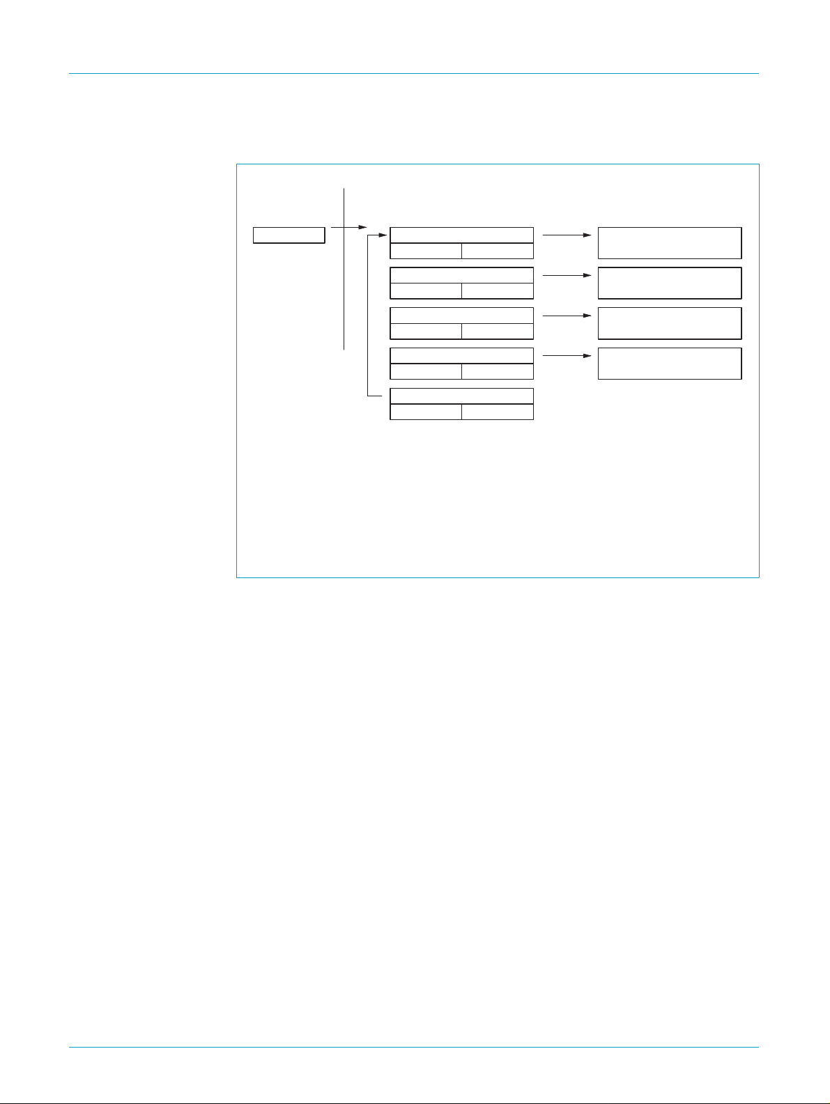
Philips Semiconductors
9.3 Continuous circular queue example
UCB1500
PCI to AC97 bridge/host controller
CB1500 REGISTER
DTP
0
1
2
3
4
(1) In this example, descriptor entry 5 points to the beginning of the descriptor table.
(2) The descriptor entries are processed in sequence, from 0 to 4, then loops back to 0.
(3) Each data buffer can be a maximum of 64k in size, and does not have to be sequential in
memory.
(4) If the Interrupt bit of an entry is set, it can generate a ‘Done’ interrupt provided that the
corresponding interrupt is enabled.
DESCRIPTOR TABLE
DT=1 DT Link=1
MEMORY
DATA
Fig 5. Continuous circular queue example
SC00210
9.3.1 Transmit algorithm
1. Create a transmit DT using the circular queue configuration.
2. Intialize UCB1500 DMA registers
Set the transmit DTP Invalid Bit Mask of the DMA channel in use.
•
Start transmission, while monitoring transmit done interrupt.
•
At transmit done interrupt, examine transmit DT index and Byte counter to
•
perform buffer management, if required.
9.3.2 Receive algorithm
1. Create a receive DT using the circular queue configuration.
2. Initialize UCB1500 DMA registers (refer to Section 8.1).
a. Set the receive DTP Invalid Bit Mask of the DMA channel in use.
b. Start transmission, while monitoring receive done interrupt.
c. At receive done interrupt, examine receive DT index and Byte counter to
perform buffer management, if required.
9397 750 06854
Objective specification Rev. 01 — 4 February 2000 46 of 58
© Philips Electronics N.V. 2000. All rights reserved.
Page 47

Philips Semiconductors
10. Limiting values
10.1 Maximum ratings
Table 71: Maximum ratings
Symbol Parameter Conditions Min Max Unit
T
stg
V
CC
V
i
[1] Stresses greater than those listed under MAXIMUM RATINGS may cause permanent damage to the
10.2 Recommended operating conditions
Table 72: Recommended operating conditions
Symbol Parameter Conditions Min Typ Max Unit
V
DD
V
i
V
o
T
amb
UCB1500
PCI to AC97 bridge/host controller
storage temperature -40 +125 °C
supply voltage -0.5 +4.6 V
DC input voltage -0.5 +6.0 V
device. This is a stress rating only and functional operation of the device at these or any conditions
above those indicated in the operational sections of this specification is not implied. Exposure to
absolute maximum rating conditions for extended periods of time may affect reliability.
supply voltage 3.0 3.3 3.6 V
input voltage 0 5.5 V
output voltage output active 0 V
operating free-air
0 +70 °C
temperature
DD
V
11. Static characteristics
Table 73: DC Characteristics
VCC= 3.3 V
Symbol Parameter Conditions Min Typ Max Unit
V
IH
V
IL
V
hyst
V
OH
V
OL
I
OH
I
OL
I
OH
I
OL
HIGH level input voltage 2.0 V
LOW level input voltage 0.8 V
Hysteresis voltage 0.4 V
HIGH level output voltage IOH= −4mA VDD−0.4 V
LOW level output voltage IOL=+4mA 0.4 V
HIGH level output current 5 ns slew rate output;
V
OH=VDD
−0.4 V
LOW level output current 5 ns slew rate output;
= 0.4 V
V
OL
-4.0 mA
4.0 mA
HIGH level short current 4 mA output; VOH=0V −60 mA
5 ns slew rate output;
=0V
V
OH
LOW level short current 4 mA output; VOL=V
5 ns slew rate output;
V
OL=VDD
DD
−60 mA
60 mA
60 mA
9397 750 06854
Objective specification Rev. 01 — 4 February 2000 47 of 58
© Philips Electronics N.V. 2000. All rights reserved.
Page 48

Philips Semiconductors
UCB1500
PCI to AC97 bridge/host controller
12. Dynamic characteristics
Table 74: AC Characteristics
VCC= 3.3 V
Symbol Parameter Conditions Min Typ Max Unit
I
OH(AC)
I
OL(AC)
I
OL
slew
slew
Switching current
HIGH
(test point) V
Switching current LOW V
(test point) V
LOW clamp current −5V<Vin< −1V mA
r
f
Output rise slew rate 0.4 V to 2.4 V load 1 3.3 V/ns
Output fall slew rate 2.4 V to 0.4 V load 1 3.3 V/ns
0 V < V
1.4 V < V
3.1 V < V
out
out
2.2 V > V
0.71 V > V
out
< 1.4 V −44 mA
out
< 2.4 V mA
out
out<VDD
44–
+
V
( 1.4 )–
out
----------------------------- -
0.024
Eqt’n A mA
= 3.1 V −142 mA
> 2.2 V 95 mA
> 0.55 V mA
out
> −1 V Eqt’n B
out
V
out
-------------
0.023
= 0.71 V 206 mA
V
1+()
in
25–
+
----------------------
0.015
13. Clock and timing specification
13.1 PCI clock timing
Table 75: PCI clock timing
Frequency = 33 MHz
Symbol Parameter Min Max Unit
T
cyc
T
high
T
low
13.2 PCI timing parameters
Table 76: PCI timing parameters
Frequency = 33 MHz
Symbol Parameter Min Max Unit
T
val
T
on
T
off
T
su
T
h
T
rst-clk
T
rst-off
PCICLK cycle time 30 ns
PCICLK HIGH time 11 ns
PCICLK LOW time 11 ns
PCICLK slew rate 1 4 V/ns
PCICLK to signal valid delay 2 11 ns
Float to active delay 2 ns
Active to float delay 28 ns
Input setup time to PCICLK 7 ns
Input hold time from PCICLK 0 ns
Reset active time after PCICLK stable 100 µs
Reset active to output float delay 40 ns
9397 750 06854
Objective specification Rev. 01 — 4 February 2000 48 of 58
© Philips Electronics N.V. 2000. All rights reserved.
Page 49
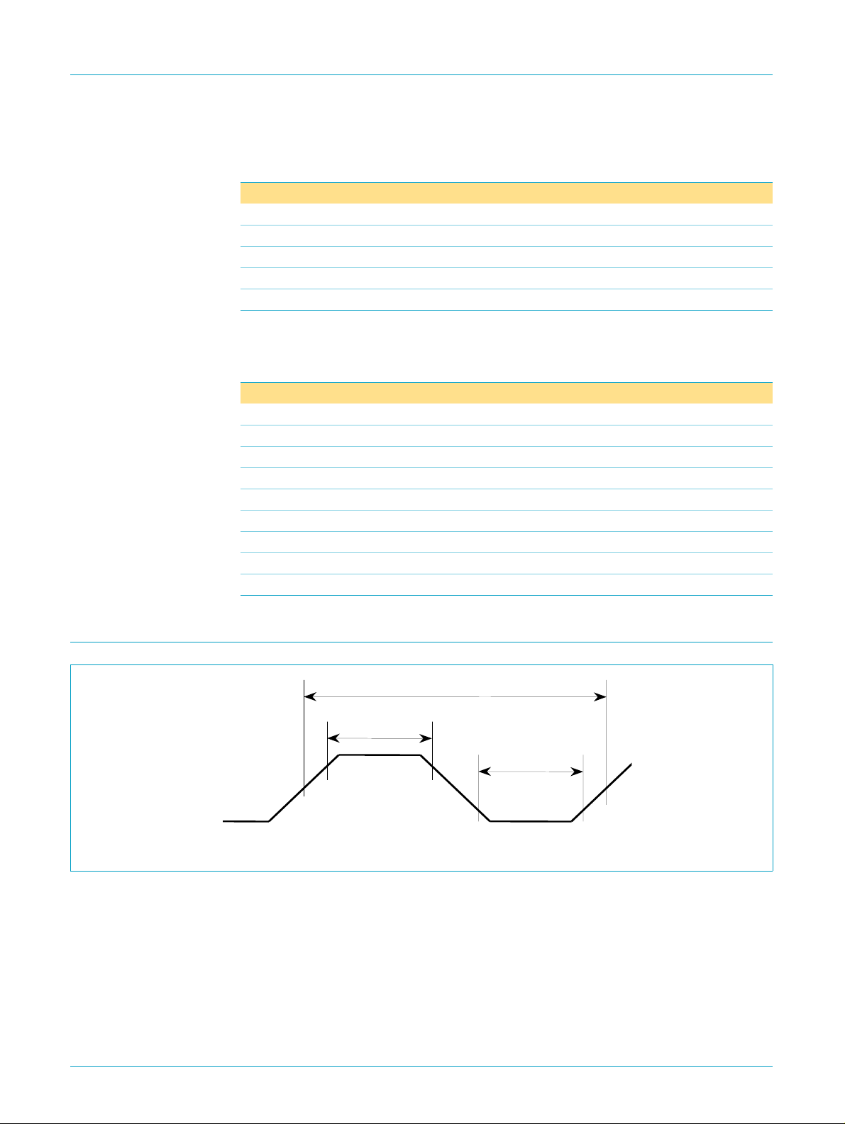
Philips Semiconductors
13.3 EEPROM clock timing
Table 77: EEPROM clock timing
Symbol Parameter Min Max Unit
T
low
T
high
T
pelh
T
pehl
13.4 EEPROM timing parameters
Table 78: EEPROM timing parameters
Symbol Parameter Min Max Unit
T
SU;STA
T
SU;STO
T
HD;STA
T
HD;STO
T
SU;DAT
T
HD;DAT
T
HD
T
AA
T
WR
UCB1500
PCI to AC97 bridge/host controller
EEPCLK frequency 0 129 kHz
EEPCLK HIGH time 3.7 µs
EEPCLK LOW time 3 µs
PCI clock rising edge to EEPCLK rising edge 8.03 ns
PCI clock rising edge to EEPCLK falling edge 7.75 ns
Start condition setup time 3.7 µs
Stop condition setup time 3.7 µs
Start condition hold time 3 µs
Stop condition hold time 3 µs
Data in setup time 250 ns
Data in hold time 0 ns
Data out hold time 0 ns
Clock to output 0.3 3.5 µs
Write cycle time 10 ms
14. System timing
Fig 6. 3.3 V clock waveform
T_cyc
T_high
T_low
9397 750 06854
Objective specification Rev. 01 — 4 February 2000 49 of 58
© Philips Electronics N.V. 2000. All rights reserved.
Page 50
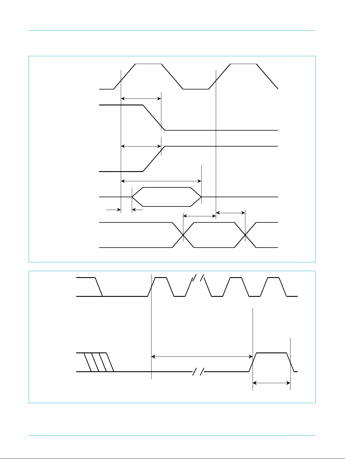
Philips Semiconductors
CLK
OUTPUT
DELAY
OUTPUT
DELAY
Tri-State
OUTPUT
T_off
T_fval
T_rval
T_off
T_su
UCB1500
PCI to AC97 bridge/host controller
T_h
INPUT
Fig 7. Input, output timing measurement conditions
PCICLK
RST#
Fig 8. PCI reset timing diagram
T_rst-clk
T_rst-off
9397 750 06854
Objective specification Rev. 01 — 4 February 2000 50 of 58
© Philips Electronics N.V. 2000. All rights reserved.
Page 51
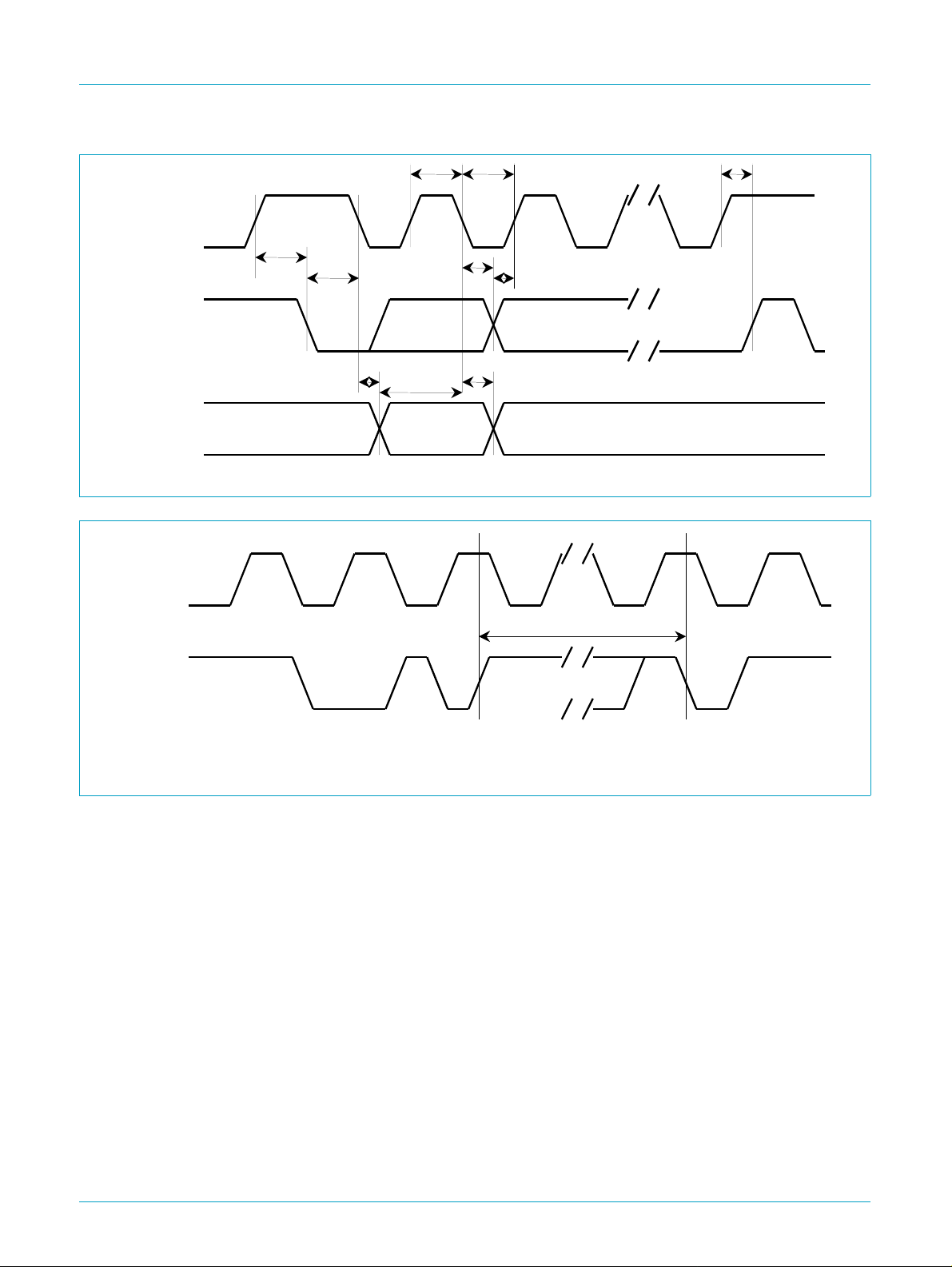
Philips Semiconductors
UCB1500
PCI to AC97 bridge/host controller
EEPCLK
T_su :sta
EEPD
(in)
EEPD
(out)
Fig 9. EEPROM bus timing
EEPCLK
T_hd :sta
T_hd :dat
T_aa T_hd :sto
T_lowT_high
T_su :dat
T_hd
T_su :sto
T_wr
EEPD
Fig 10. EEPROM write cycle
ACK
STOP
Condition
START
Condition
9397 750 06854
Objective specification Rev. 01 — 4 February 2000 51 of 58
© Philips Electronics N.V. 2000. All rights reserved.
Page 52
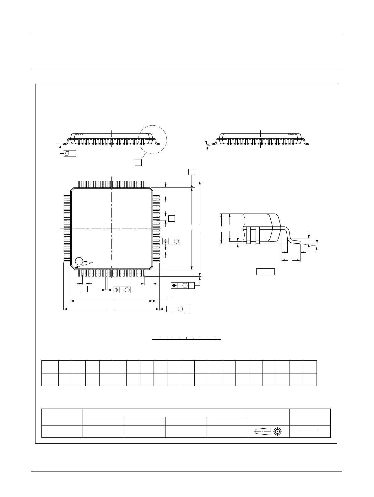
Philips Semiconductors
15. Package outline
UCB1500
PCI to AC97 bridge/host controller
LQFP80: plastic low profile quad flat package; 80 leads; body 12 x 12 x 1.4 mm
c
y
X
A
60 41
61
e
pin 1 index
b
p
D
H
w M
D
80
1
Z
40
E
e
H
E
E
w M
b
p
21
20
Z
D
v M
A
B
v M
B
A
2
A
A
1
detail X
SOT315-1
(A )
3
θ
L
p
L
0 5 10 mm
scale
DIMENSIONS (mm are the original dimensions)
mm
OUTLINE
VERSION
SOT315-1
A
A1A2A3bpcE
max.
0.16
1.6
0.04
1.5
1.3
0.27
0.13
0.18
0.12
0.25
IEC JEDEC EIAJ
UNIT
Note
1. Plastic or metal protrusions of 0.25 mm maximum per side are not included.
(1)
(1) (1)(1)
D
12.1
11.9
REFERENCES
eHELL
H
D
0.5
14.15
13.85
14.15
13.85
12.1
11.9
0.75
0.30
p
0.15 0.10.21.0
EUROPEAN
PROJECTION
Z
1.45
1.05
D
Zywv θ
E
1.45
1.05
ISSUE DATE
95-12-19
97-07-15
o
7
o
0
Fig 11. LQFP80 (SOT315-1)
9397 750 06854
Objective specification Rev. 01 — 4 February 2000 52 of 58
© Philips Electronics N.V. 2000. All rights reserved.
Page 53

Philips Semiconductors
16. Soldering
16.1 Introduction to soldering surface mount packages
This text gives a very brief insight to a complex technology. A more in-depth account
of soldering ICs can be found in our
Packages
There is no soldering method that is ideal for all surface mount IC packages. Wave
soldering is not always suitable for surface mount ICs, or for printed-circuit boards
with high population densities. In these situations reflow soldering is often used.
16.2 Reflow soldering
Reflow soldering requires solder paste (a suspension of fine solder particles, flux and
binding agent) to be applied to the printed-circuit board by screen printing, stencilling
or pressure-syringe dispensing before package placement.
Several methods exist for reflowing; for example, infrared/convection heating in a
conveyor type oven. Throughput times (preheating, soldering and cooling) vary
between 100 and 200 seconds depending on heating method.
UCB1500
PCI to AC97 bridge/host controller
Data Handbook IC26; Integrated Circuit
(document order number 9398 652 90011).
Typical reflow peak temperatures range from 215 to 250 °C. The top-surface
temperature of the packages should preferable be kept below 230 °C.
16.3 Wave soldering
Conventional single wave soldering is not recommended for surface mount devices
(SMDs) or printed-circuit boards with a high component density, as solder bridging
and non-wetting can present major problems.
To overcome these problems the double-wave soldering method was specifically
developed.
If wave soldering is used the following conditions must be observed for optimal
results:
Use a double-wave soldering method comprising a turbulent wave with high
•
upward pressure followed by a smooth laminar wave.
For packages with leads on two sides and a pitch (e):
•
– larger than or equal to 1.27 mm, the footprint longitudinal axis is preferred to be
parallel to the transport direction of the printed-circuit board;
– smaller than 1.27 mm, the footprint longitudinal axis must be parallel to the
transport direction of the printed-circuit board.
The footprint must incorporate solder thieves at the downstream end.
For packages with leads on four sides, the footprint must be placed at a 45° angle
•
to the transport direction of the printed-circuit board. The footprint must
incorporate solder thieves downstream and at the side corners.
During placement and before soldering, the package must be fixed with a droplet of
adhesive. The adhesive can be applied by screen printing, pin transfer or syringe
dispensing. The package can be soldered after the adhesive is cured.
9397 750 06854
Objective specification Rev. 01 — 4 February 2000 53 of 58
© Philips Electronics N.V. 2000. All rights reserved.
Page 54

Philips Semiconductors
Typical dwell time is 4 seconds at 250 °C. A mildly-activated flux will eliminate the
need for removal of corrosive residues in most applications.
16.4 Manual soldering
Fix the component by first soldering two diagonally-opposite end leads. Use a low
voltage (24 V or less) soldering iron applied to the flat part of the lead. Contact time
must be limited to 10 seconds at up to 300 °C.
When using a dedicated tool, all other leads can be soldered in one operation within
2 to 5 seconds between 270 and 320 °C.
16.5 Package related soldering information
Table 79: Suitability of surface mount IC packages for wave and reflow soldering
Package Soldering method
BGA, LFBGA, SQFP, TFBGA not suitable suitable
HBCC, HLQFP, HSQFP, HSOP, HTQFP,
HTSSOP, SMS
PLCC
LQFP, QFP, TQFP not recommended
SSOP, TSSOP, VSO not recommended
UCB1500
PCI to AC97 bridge/host controller
methods
Wave Reflow
not suitable
[3]
, SO, SOJ suitable suitable
[2]
[3] [4]
[5]
suitable
suitable
suitable
[1]
[1] All surface mount (SMD) packages are moisture sensitive. Depending upon the moisture content, the
maximum temperature (with respect to time) and body size of the package, there is a risk that internal
or external package cracks may occur due to vaporization of the moisture in them (the so called
popcorn effect). For details, refer to the Drypack information in the
Circuit Packages; Section: Packing Methods
[2] These packages are not suitable for wave soldering as a solder joint between the printed-circuit board
and heatsink (at bottom version) can not be achieved, and as solder may stick to the heatsink (on top
version).
[3] If wave soldering is considered, then the package must be placed at a 45° angle to the solder wave
direction. The package footprint must incorporate solder thieves downstream and at the side corners.
[4] Wave soldering is only suitable for LQFP, QFP and TQFP packages with a pitch (e) equal to or larger
than 0.8 mm; it is definitely not suitable for packages with a pitch (e) equal to or smaller than 0.65 mm.
[5] Wave soldering is only suitable for SSOP and TSSOP packages with a pitch (e) equal to or larger than
0.65 mm; it is definitely not suitable for packages with a pitch (e) equal to or smaller than 0.5mm.
.
Data Handbook IC26; Integrated
9397 750 06854
Objective specification Rev. 01 — 4 February 2000 54 of 58
© Philips Electronics N.V. 2000. All rights reserved.
Page 55

Philips Semiconductors
PCI to AC97 bridge/host controller
UCB1500
17. Revision history
Table 80: Revision history
Rev Date CPCN Description
01 000204 The format of this specification has be redesigned to comply with Philips Semiconductors
new presentation and information standard.
9397 750 06854
Objective specification Rev. 01 — 4 February 2000 55 of 58
© Philips Electronics N.V. 2000. All rights reserved.
Page 56

Philips Semiconductors
PCI to AC97 bridge/host controller
18.Data sheet status
UCB1500
Datasheet status Product status Definition
Objective specification Development This data sheet contains the design target or goal specifications for product development. Specification may
change in any manner without notice.
Preliminary specification Qualification This data sheet contains preliminary data, and supplementary data will be published at a later date. Philips
Semiconductors reserves the right to make changes at any time without notice in order to improve design and
supply the best possible product.
Product specification Production This data sheet contains final specifications. Philips Semiconductors reserves the right to make changes at any
time without notice in order to improve design and supply the best possible product.
[1] Please consult the most recently issued data sheet before initiating or completing a design.
19.Definitions
Short-form specification —Thedatainashort-formspecificationis
extractedfromafulldatasheetwiththesametypenumberandtitle.For
detailed information see the relevant data sheet or data handbook.
Limiting values definition —Limitingvaluesgivenareinaccordancewith
theAbsoluteMaximumRatingSystem(IEC60134).Stressaboveoneor
moreofthelimitingvaluesmaycausepermanentdamagetothedevice.
Thesearestressratingsonlyandoperationofthedeviceattheseoratany
otherconditionsabovethosegivenintheCharacteristicssectionsofthe
specificationisnotimplied.Exposuretolimitingvaluesforextendedperiods
may affect device reliability.
Application information —Applicationsthataredescribedhereinforany
oftheseproductsareforillustrativepurposesonly.PhilipsSemiconductors
makenorepresentationorwarrantythatsuchapplicationswillbesuitablefor
the specified use without further testing or modification.
[1]
20.Disclaimers
Life support —Theseproductsarenotdesignedforuseinlifesupport
appliances,devices,orsystemswheremalfunctionoftheseproductscan
reasonablybeexpectedtoresultinpersonalinjury.PhilipsSemiconductors
customersusingorsellingtheseproductsforuseinsuchapplicationsdoso
attheirownriskandagreetofullyindemnifyPhilipsSemiconductorsforany
damages resulting from such application.
Right to make changes —PhilipsSemiconductorsreservestherightto
makechanges,withoutnotice,intheproducts,includingcircuits,standard
cells,and/orsoftware,describedorcontainedhereininordertoimprove
design and/or performance. Philips Semiconductors assumes no
responsibilityorliabilityfortheuseofanyoftheseproducts,conveysno
licenceortitleunderanypatent,copyright,ormaskworkrighttothese
products,andmakesnorepresentationsorwarrantiesthattheseproducts
arefreefrompatent,copyright,ormaskworkrightinfringement,unless
otherwise specified.
9397 750 06854
© Philips Electronics N.V. 2000 All rights reserved.
Objective specification Rev. 01 — 4 February 2000 56 of 58
Page 57

Philips Semiconductors
PCI to AC97 bridge/host controller
Philips Semiconductors - a worldwide company
UCB1500
Argentina: see South America
Australia: Tel.+61297048141,Fax.+61297048139
Austria: Tel. +43160101, Fax.+431601011210
Belarus: Tel. +37517 220 0733, Fax.+37517 220 0773
Belgium: see The Netherlands
Brazil:see South America
Bulgaria: Tel. +359268 9211, Fax.+359268 9102
Canada: Tel. +18002347381
China/Hong Kong: Tel. +852 2 3197888, Fax.+8522 3197700
Colombia: see South America
Czech Republic: see Austria
Denmark: Tel. +453 2882636, Fax.+453 1570044
Finland: Tel. +3589615800, Fax.+358961580920
France: Tel. +33140996161, Fax.+33140996427
Germany: Tel. +4940235360, Fax.+49402353 6300
Hungary: see Austria
India: Tel. +91224938541, Fax.+91224938722
Indonesia: see Singapore
Ireland: Tel. +35317640000, Fax.+35317640200
Israel: Tel. +97236450444, Fax.+97236491007
Italy: Tel. +390392036838,Fax +390392036800
Japan: Tel. +81337405130, Fax.+81337405057
Korea: Tel. +8227091412, Fax.+8227091415
Malaysia: Tel. +60 37505214, Fax.+6037574880
Mexico: Tel. +9-58002347381
Middle East: see Italy
Netherlands: Tel. +31402782785, Fax.+31402788399
New Zealand: Tel. +6498494160, Fax.+6498497811
Norway: Tel. +4722748000, Fax.+4722748341
Philippines: Tel. +6328166380, Fax.+6328173474
Poland: Tel. +48225710000, Fax.+48225710001
Portugal: see Spain
Romania: see Italy
Russia: Tel. +70957556918, Fax.+70957556919
Singapore: Tel. +653502538, Fax.+652516500
Slovakia: see Austria
Slovenia: see Italy
South Africa: Tel. +27114715401, Fax.+27114715398
South America: Tel. +55118212333, Fax.+55118291849
Spain: Tel. +3433016312, Fax.+3433014107
Sweden: Tel. +4686322000, Fax.+4686322745
Switzerland: Tel. +4114882686, Fax.+4114817730
Taiwan: Tel. +886221342865, Fax.+886221342874
Thailand: Tel. +6627454090, Fax.+6623980793
Turkey: Tel. +902165221500, Fax.+902165221813
Ukraine: Tel. +380442642776, Fax.+380442680461
United Kingdom: Tel. +442087305000, Fax.+442087548421
United States: Tel. +18002347381
Uruguay: see South America
Vietnam: see Singapore
Yugoslavia: Tel. +38111625344, Fax.+38111635777
For all other countries apply to: Philips Semiconductors,
InternationalMarketing&SalesCommunications,
BuildingBE, P.O.Box218, 5600MDEINDHOVEN,
TheNetherlands,Fax.+31402724825
Internet:http://www.semiconductors.philips.com
(SCA68)
9397 750 06854
Objective specification Rev. 01 — 4 February 2000 57 of 58
© Philips Electronics N.V. 2000. All rights reserved.
Page 58

Philips Semiconductors
PCI to AC97 bridge/host controller
Contents
1 General description. . . . . . . . . . . . . . . . . . . . . . 1
2 Features . . . . . . . . . . . . . . . . . . . . . . . . . . . . . . . 1
3 Applications. . . . . . . . . . . . . . . . . . . . . . . . . . . . 2
4 Ordering information. . . . . . . . . . . . . . . . . . . . . 2
5 Block diagram . . . . . . . . . . . . . . . . . . . . . . . . . . 2
6 Pinning information. . . . . . . . . . . . . . . . . . . . . . 3
6.1 Pinning . . . . . . . . . . . . . . . . . . . . . . . . . . . . . . . 3
6.2 Pin description . . . . . . . . . . . . . . . . . . . . . . . . . 3
7 PCI configuration space . . . . . . . . . . . . . . . . . . 5
7.1 Overview. . . . . . . . . . . . . . . . . . . . . . . . . . . . . . 5
7.2 Configuration registers . . . . . . . . . . . . . . . . . . . 6
8 Control Registers. . . . . . . . . . . . . . . . . . . . . . . 20
8.1 DMA Registers . . . . . . . . . . . . . . . . . . . . . . . . 20
8.2 Interrupt Controller Registers . . . . . . . . . . . . . 27
8.3 General purpose counters . . . . . . . . . . . . . . . 30
8.4 EEPROM . . . . . . . . . . . . . . . . . . . . . . . . . . . . 31
8.5 DMA counter control. . . . . . . . . . . . . . . . . . . . 32
8.6 AC-97 registers. . . . . . . . . . . . . . . . . . . . . . . . 32
8.7 Status port registers . . . . . . . . . . . . . . . . . . . . 42
9 DMA engine application notes . . . . . . . . . . . . 43
9.1 Transmit Descriptor Table format. . . . . . . . . . 44
9.2 Receive Descriptor Table format . . . . . . . . . . 45
9.3 Continuous circular queue example. . . . . . . . 46
10 Limiting values. . . . . . . . . . . . . . . . . . . . . . . . . 47
10.1 Maximum ratings . . . . . . . . . . . . . . . . . . . . . . 47
10.2 Recommended operating conditions . . . . . . . 47
11 Static characteristics. . . . . . . . . . . . . . . . . . . . 47
12 Dynamic characteristics . . . . . . . . . . . . . . . . . 48
13 Clock and timing specification. . . . . . . . . . . . 48
13.1 PCI clock timing . . . . . . . . . . . . . . . . . . . . . . . 48
13.2 PCI timing parameters . . . . . . . . . . . . . . . . . . 48
13.3 EEPROM clock timing . . . . . . . . . . . . . . . . . . 49
13.4 EEPROM timing parameters . . . . . . . . . . . . . 49
14 System timing . . . . . . . . . . . . . . . . . . . . . . . . . 49
15 Package outline . . . . . . . . . . . . . . . . . . . . . . . . 52
16 Soldering . . . . . . . . . . . . . . . . . . . . . . . . . . . . . 53
16.1 Introduction to soldering surface mount
packages. . . . . . . . . . . . . . . . . . . . . . . . . . . . 53
16.2 Reflow soldering. . . . . . . . . . . . . . . . . . . . . . . 53
16.3 Wave soldering. . . . . . . . . . . . . . . . . . . . . . . . 53
16.4 Manual soldering . . . . . . . . . . . . . . . . . . . . . . 54
16.5 Package related soldering information. . . . . . 54
17 Revision history. . . . . . . . . . . . . . . . . . . . . . . . 55
18 Data sheet status. . . . . . . . . . . . . . . . . . . . . . . 56
19 Definitions . . . . . . . . . . . . . . . . . . . . . . . . . . . . 56
20 Disclaimers. . . . . . . . . . . . . . . . . . . . . . . . . . . . 56
UCB1500
© Philips Electronics N.V. 2000. Printed in the U.S.A.
Allrightsarereserved.Reproductioninwholeorinpartisprohibitedwithouttheprior
written consent of the copyright owner.
Theinformationpresentedinthisdocumentdoesnotformpartofanyquotationor
contract,isbelievedtobeaccurateandreliableandmaybechangedwithoutnotice.No
liabilitywillbeacceptedbythepublisherforanyconsequenceofitsuse.Publication
thereofdoesnotconveynorimplyanylicenseunderpatent-orotherindustrialor
intellectual property rights.
Date of release: 4 February 2000 Document order number: 9397 750 06854
 Loading...