

Datasheet UCC1580-1, UCC1580-2, UCC1580-3, UCC1580-4, UCC2580-1 Datasheet (TEXAS INSTRUMENTS)
...Page 1
Single Ended Active Clamp/Reset PWM
UCC1580-1,-2,-3,-4
UCC2580-1,-2,-3,-4
UCC3580-1,-2,-3,-4
FEATURES
Provides Auxiliary Switch Activation
Complementary to Main Power
Switch Drive
Programmable deadtime (Turn-on
Delay) Between Activation of Each
Switch
Voltage Mode Control with
Feedforward Operation
Programmable Limits for Both
Transformer Volt- Second Product
and PWM Duty Cycle
High Current Gate Driver for Both
Main and Auxiliary Outputs
Multiple Protection Features with
Latched Shutdown and Soft Restart
Low Supply Current (100 mA Startup,
1.5 mA Operation)
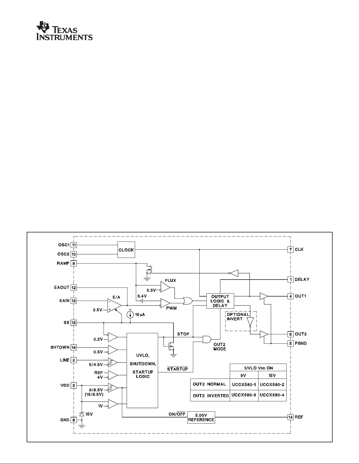
BLOCK DIAGRAM
DESCRIPTION
The UCC3580 family of PWM controllers is designed to implement a variety
of active clamp/reset and synchronous rectifier switching converter topologies. While containing all the necessary functions for fixed frequency, high
performance pulse width modulation, the additional feature of this design is
the inclusion of an auxiliary switch driver which complements the main
power switch, and with a programmable deadtime or delay between each
transition. The active clamp/reset technique allows operation of single
ended converters beyond 50% duty cycle while reducing voltage stresses
on the switches, and allows a greater flux swing for the power transformer.
This approach also allows a reduction in switching losses by recovering energy stored in parasitic elements such as leakage inductance and switch
capacitance.
The oscillator is programmed with two resistors and a capacitor to set
switching frequency and maximum duty cycle. A separate synchronized
ramp provides a voltage feedforward pulse width modulation and a programmed maximum volt-second limit. The generated clock from the oscillator contains both frequency and maximum duty cycle information.
(continued)
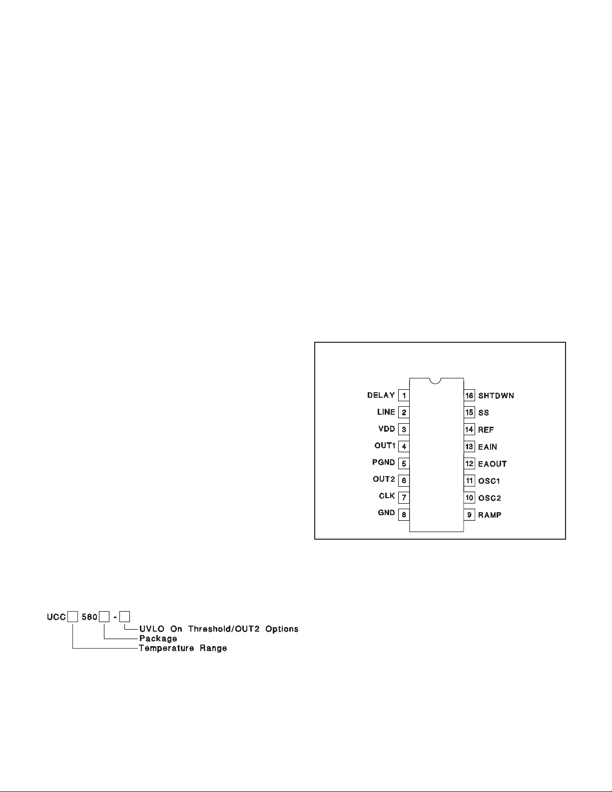
Pin Numbers refer to DIL-16 and SOIC-16 packages
SLUS292D - FEBRUARY 1999 - REVISED FEBRUARY 2007
UDG-95069-2
Page 2
DESCRIPTION (cont.)
The main gate drive output (OUT1) is controlled by the
pulse width modulator. The second output (OUT2) is intended to activate an auxiliary switch during the off time
of the main switch, except that between each transition
there is deadtime where both switches are off, programmed by a single external resistor. This design offers
two options for OUT2, normal and inverted. In the -1 and
-2 versions, OUT2 is normal and can be used to drive
PMOS FETs. In the -3 and -4 versions, OUT2 is inverted
and can be used to drive NMOS FETs. In all versions,
both the main and auxiliary switches are held off prior to
startup and when the PWM command goes to zero duty
cycle. During fault conditions, OUT1 is held off while
OUT2 operates at maximum duty cycle with a guaranteed off time equal to the sum of the two deadtimes.
UCC1580-1,-2,-3,-4
UCC2580-1,-2,-3,-4
UCC3580-1,-2,-3,-4
Undervoltage lockout monitors supply voltage (VDD), the
precision reference (REF), input line voltage (LINE), and
the shutdown comparator (SHTDWN). If after any of
these four have sensed a fault condition, recovery to full
operation is initiated with a soft start. VDD thresholds, on
and off, are 15V and 8.5V for the -2 and -4 versions, 9V
and 8.5V for the -1 and -3 versions.
The UCC1580-x is specified for operation over the military temperature range of
UCC2580-x is specified from -40°C to 85°C. The
UCC3580-x is specified from
tions include 16-pin surface mount and dual in-line.
-
55°C to 125°C. The
0°C to 70°C. Package op-
ABSOLUTE MAXIMUM RATINGS CONNECTION DIAGRAMS
VDD...........................................16V
I
..........................................25mA
VDD
LINE, RAMP ........................ 0.3V to VDD + 1V
I
LINE,IRAMP
DELAY ........................................5.3V
I
DELAY
I
OUT1
I
OUT2
I
................................ 100mA to 100mA
CLK
OSC1, OSC2, SS, SHTDWN, EAIN ..... 0.3V to REF + 0.3V
I
EAOUT
I
......................................... 30mA
REF
PGND.................................. 0.2V to 0.2V
Storage Temperature ..................
Junction Temperature..................
Lead Temperature (Soldering, 10 sec.).............+300°C
All voltages are with respect to ground unless otherwise stated.
Currents are positive into, negative out of the specified terminal. Consult Packaging Section of Databook for thermal limitations and considerations of packages.
.....................................5mA
........................................ 5mA
(tpw < 1 s and Duty Cycle < 10%) ....... 0.6A to 1.2A
(tpw < 1 s and Duty Cycle < 10%) ....... 0.4A to 0.4A
.................................. 5mAto5mA
-65°C to +150°C
-55°C to +150°C
DIL-16, SOIC-16 (Top View)
J, N, or D Packages
ORDER INFORMATION
2
Page 3

UCC1580-1,-2,-3,-4
UCC2580-1,-2,-3,-4
UCC3580-1,-2,-3,-4
ELECTRICAL CHARACTERISTICS
12V, R1 = 18.2 kW , R2 = 4.41 kW ,C
-40°C to 85°C for the UCC2580, -55°C to 125°C for the UCC1580, T
T
Unless otherwise stated, all specifications are over the full temperature range, VDD =
= 130 pF, R3 = 100 kW ,C
OUT1
=0F,C
A=TJ
=0F.TA= 0°C to 70°C for the UCC3580,
OUT2
.
PARAMETER TEST CONDITIONS MIN TYP MAX UNITS
Oscillator Section
Frequency 370 400 430 kHz
CLK Pulse Width 650 750 850 ns
I
CLK V
CLK V
OH
OL
= 3 mA 4.3 4.7 V
CLK
I
= 3 mA 0.3 0.5 V
CLK
Ramp Generator Section
I
Ramp V
OL
= 100 mA 50 100 mV
RAMP
Flux Comparator Vth 3.16 3.33 3.50 V
Pulse Width Modulator Section
Minimum Duty Cycle OUT1, EAOUT = VOL 0 %
Maximum Duty Cycle OUT1, EAIN = 2.6 V 63 66 69 %
PWM Comparator Offset 0.1 0.4 0.9 V
Error Amplifier Section
EAIN EAOUT = EAIN 2.44 2.5 2.56 V
I
EAIN
EAOUT, VOL EAIN = 2.6 V, I
EAOUT, VOH EAIN = 2.4 V, I
EAOUT = EAIN 150 400 nA
= 100 mA 0.3 0.5 V
EAOUT
= 100 mA 4 5 5.5 V
EAOUT
AVOL 70 80 dB
Gain Bandwidth Product f = 100 kHz (Note 1) 2 6 MHz
Softstart/Shutdown Section
Start Duty Cycle EAIN = 2.4 V 0 %
OL I
SS V
= 100 mA 100 350 mV
SS
SS Restart Threshold 400 550 mV
I
SS
SHTDWN V
I
SHTDWN
TH
0.4 0.5 0.6 V
–20 –35 mA
50 150 nA
Undervoltage Lockout Section
VDD On UCC3580-2,-4 14 15 16 V
UCC3580-1,-3 8 9 10 V
VDD Off 7.5 8.5 9.5 V
LINE On 4.7 5 5.3 V
LINE Off 4.2 4.5 4.8 V
I
LINE
LINE=6V 50 150 nA
Supply Section
VDD Clamp I
Start VDD < VDD On 160 250 A
I
VDD
Operating No Load 2.5 3.5 mA
I
VDD
=10mA 14 15 16 V
VDD
Output Drivers Section
OUT1 V
OUT1 V
OUT2 V
OUT2 V
High I
SAT
Low I
SAT
High I
SAT
Low I
SAT
OUT1 Fall Time C
OUT1 Rise Time C
OUT2 Fall Time C
OUT2 Rise Time C
= 50 mA 0.4 1.0 V
OUT1
=100 mA 0.4 1.0 V
OUT1
= 30 mA 0.4 1.0 V
OUT2
= 30 mA 0.4 1.0 V
OUT2
= 1nF, RS =3W 20 50 ns
OUT1
= 1nF, RS =3W 40 80 ns
OUT1
= 300pF, RS =10W 20 50 ns
OUT2
= 300pF, RS=10W 20 40 ns
OUT2
3
Page 4
UCC1580-1,-2,-3,-4
UCC2580-1,-2,-3,-4
UCC3580-1,-2,-3,-4
ELECTRICAL CHARACTERISTICS
12V, R1 = 18.2 kW , R2 = 4.41 kW ,C
-40°C to 85°C for the UCC2580, -55°C to 125°C for the UCC1580, T
PARAMETER TEST CONDITIONS MIN TYP MAX UNITS
Output Drivers Section (cont.)
Delay 1 OUT2 to OUT1 R3 = 100 kW,C
Delay 2 OUT1 to OUT2 R3 = 100 kW,C
Reference Section
REF I
Load Regulation I
Line Regulation VDD = 10 V to 14 V 1 20 mV
Note 1: Guaranteed by design. Not 100% tested in production.
T
Unless otherwise stated, all specifications are over the full temperature range, VDD =
= 130 pF, R3 = 100 kW ,C
T
T
= 25°C 100 120 140 ns
A=TJ
= 25°C 140 170 200 ns
A=TJ
= 0 4.875 5 5.125 V
REF
=0mAto1mA 1 20 mV
REF
=0F,C
OUT1
A=TJ
OUT1=COUT2
OUT1=COUT2
=0F.TA= 0°C to 70°C for the UCC3580,
OUT2
.
= 15 pF 90 120 160 ns
= 15 pF 110 170 250 ns
PIN DESCRIPTIONS
CLK: Oscillator clock output pin from a low impedance
CMOS driver. CLK is high during guaranteed off time.
CLK can be used to synchronized up to five other
UCC3580 PWMs.
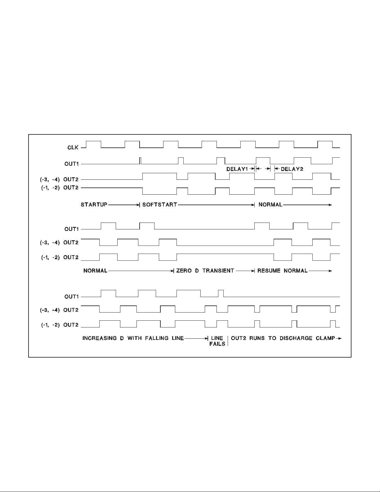
DELAY: A resistor from DELAY to GND programs the
nonoverlap delay between OUT1 and OUT2. The delay
times, Delay1 and Delay2, are shown in Figure 1 and are
as follows:
Delay pF R111 3=·.
Delay2 is designed to be larger than Delay1 by a ratio
shown in Figure 2.
EAIN: Inverting input to the error amplifier. The
noninverting input of the error amplifier is internally set to
2.5V. EAIN is used for feedback and loop compensation.
EAOUT: Output of the error amplifier and input to the
PWM comparator. Loop compensation components
connect from EAOUT to EAIN.
GND: Signal Ground.
LINE: Hysteretic comparator input. Thresholds are 5.0V
and 4.5V. Used to sense input line voltage and turn off
OUT1 when the line is low.
OSC1 & OSC2: Oscillator programming pins. A resistor
connects each pin to a timing capacitor. The resistor
connected to OSC1 sets maximum on time. The resistor
connected to OSC2 controls guaranteed off time. The
combined total sets frequency with the timing capacitor.
Frequency and maximum duty cycle are approximately
given by:
Frequency
=
R1 R CT
()( )
Maximum Duty Cycle
1.44
+· +227pF
R1
=
R1 R2
+
Maximum Duty Cycle for OUT1 is slightly less due to
Delay1 which is programmed by R3.
OUT1: Gate drive output for the main switch capable of
sourcing up to 0.5A and sinking 1A.
OUT2: Gate drive output for the auxiliary switch with
0.3A drive current capability.
PGND: Ground connection for the gate drivers. Connect
PGND to GND at a single point so that no high frequency
components of the output switching currents are in the
ground plane on the circuit board.
RAMP: A resistor (R4) from RAMP to the input voltage
and a capacitor (CR) from RAMP to GND programs the
feedforward ramp signal. RAMP is discharged to GND
when CLK is high and allowed to charge when CLK is
low. RAMP is the line feedforward sawtooth signal for the
PWM comparator. Assuming the input voltage is much
greater than 3.3V, the ramp is very linear. A flux
comparator compares the ramp signal to 3.3V to limit the
maximum allowable volt-second product:
Volt-Second Product Clamp = 3.3 • R4 • CR.
REF: Precision 5.0V reference pin. REF can supply up to
5mA to external circuits. REF is off until VDD exceeds 9V
(–1 and –3 versions) or activates the 15V clamp (–2 and
–4 versions) and turns off again when VDD droops below
8.5V. Bypass REF to GND with a 1mF capacitor.
SHTDWN: Comparator input to stop the chip. The
threshold is 0.5V. When the chip is stopped, OUT1 is low
and OUT2 continues to oscillate with guaranteed off time
equal to two non-overlap delay times. OUT2 continues to
switch after SHTDWN is asserted until the voltage on
VDD falls below VCS (typically 4 V) in order to discharge
the clamp capacitor.
4
Page 5
PIN DESCRIPTIONS (cont.)
SS: A capacitor from SS to ground programs the soft
start time. During soft start, EAOUT follows the amplitude
of SS’s slowly increasing waveform until regulation is
achieved.
APPLICATION INFORMATION
UCC1580-1,-2,-3,-4
UCC2580-1,-2,-3,-4
UCC3580-1,-2,-3,-4
VDD: Chip power supply pin. VDD should be bypassed
to PGND. The –1 and –3 versions require VDD to ex
ceed 9V to start and remain above 8.5V to continue run
ning. A shunt clamp from VDD to GND limits the supply
voltage to 15V. The –2 and –4 versions do not start until
-
-
Note: Waveforms are not to scale.
Figure 1. Output time relationships.
UVLO and Startup
For self biased off-line applications, -2 and -4 versions
(UVLO on and off thresholds of 15V and 8.5V typical)
are recommended. For all other applications, -1 and -3
versions provide the lower on threshold of 9V. The IC re
quires a low startup current of only 160mA when VDD is
under the UVLO threshold, enabling use of a large trickle
charge resistor (with corresponding low power dissipa
tion) from the input voltage. VDD has an internal clamp
at 15V which can sink up to 10mA. Measures should be
taken not to exceed this current. For -2 and -4 versions,
this clamp must be activated as an indication of reaching
the UVLO on threshold. The internal reference (REF) is
brought up when the UVLO on threshold is crossed. The
startup logic ensures that LINE and REF are above and
SHTDWN is below their respective thresholds before
outputs are asserted. LINE input is useful for monitoring
actual input voltage and shutting off the IC if it falls be
low a programmed value. A resistive divider should be
used to connect the input voltage to the LINE input. This
feature can protect the power supply from excessive
currents at low line voltages.
5
UDG-95070-2
-
Page 6
APPLICATION INFORMATION (cont.)
Delay Times
1400
DelayRatio
1200
1000
800
600
Delay ns
400
200
0
0 100 200 300 400 500 600 700 800 900 1000
Figure 2. Delay times.
Delay2
R3 ProgrammingResistor k
W
Delay1
1.80
1.70
1.60
1.50
1.40
1.30
1.20
1.10
UCC1580-1,-2,-3,-4
UCC2580-1,-2,-3,-4
UCC3580-1,-2,-3,-4
The soft start pin provides an effective means to start
the IC in a controlled manner. An internal current of
20 A begins charging a capacitor connected to SS once
the startup conditions listed above have been met. The
voltage on SS effectively controls maximum duty cycle
on OUT1 during the charging period. OUT2 is also con
trolled during this period (see Figure 1). Negation of any
of the startup conditions causes SS to be immediately
discharged. Internal circuitry ensures full discharge of
SS (to 0.3V) before allowing charging to begin again,
provided all the startup conditions are again met.
Delay2/Delay1 Ratio
Oscillator
Simplified oscillator block diagram and waveforms are
shown in Figure 3. OSC1 and OSC2 pins are used to
program the frequency and maximum duty cycle. Capac
itor CT is alternately charged through R1 and discharged
through R2 between levels of 1.67 V and 3.3 V. The
charging and discharging equations for CT are given by
t
2
REF
-
ö
t
1
3
÷
ø
t
-
t
2
æ
VC(charge) = • 1 • e
VC(dis ch a rg e ) = V e
ç
V
REF
è
2
··
3
-
-
-
Figure 3. Oscillator and ramp circuits.
UDG-96016-1
where t1=R1•CT andt2= R2 • CT. The charge time
and discharge time are given by
CH = 0.69 • R1 • CT and tDIS =0.69•R2•CT
t
The CLK output is high during the discharge period. It
blanks the output to limit the maximum duty cycle of
OUT1. The frequency and maximum duty cycle are
given by
Frequency =
(R1+ R2)• CT + 27 pF
Maximum Duty Cycle =
1.44
()
R1
R1+ R2
Maximum Duty Cycle for OUT1 will be slightly less due
to Delay1 which is programmed by R3.
Voltage Feedforward and Volt-Second Clamp
UCC3580 has a provision for input voltage feedforward.
As shown in Figure 3, the ramp slope is made propor
tional to input line voltage by converting it into a charging
current for CR. This provides a first order cancellation of
the effects of line voltage changes on converter perfor
mance. The maximum volt-second clamp is provided to
protect against transient saturation of the transformer
core. It terminates the OUT1 pulse when the RAMP volt
age exceeds 3.3V. If the feedforward feature is not used,
the ramp can be generated by tying R4 to REF. How
ever, the linearity of ramp suffers and in this case the
maximum volt-second clamp is no longer available.
6
-
-
-
-
Page 7

APPLICATION INFORMATION (cont.)
Output Configurations
The UCC3580 family of ICs is designed to provide con
trol functions for single ended active clamp circuits. For
different implementations of the active clamp approach,
different drive waveforms for the two switches (main and
auxiliary) are required. The -3 and -4 versions of the IC
supply complementary non-overlapping waveforms
(OUT1 and OUT2) with programmable delay which can
be used to drive the main and auxiliary switches. Most
active clamp configurations will require one of these out
puts to be transformer coupled to drive a floating switch
(e.g. Figure 5). The -1 and -2 versions have the phase of
OUT2 inverted to give overlapping waveforms. This con
figuration is suitable for capacity coupled driving of a
ground referenced p-channel auxiliary switch with the
OUT2 drive while OUT1 is directly driving an n-channel
main switch (e.g. Figure 4).
The programmable delay can be judiciously used to get
zero voltage turn-on of both the main and auxiliary
switches in the active clamp circuits. For the UCC3580,
UCC1580-1,-2,-3,-4
UCC2580-1,-2,-3,-4
UCC3580-1,-2,-3,-4
a single pin is used to program the delays between
OUT1 and OUT2 on both sets of edges. Figure 1 shows
the relationships between the outputs. Figure 2 gives the
ratio between the two delays. During the transition from
main to auxiliary switch, the delay is not very critical for
ZVS turn-on. For the first half of OUT1 off-time, the body
diode of the auxiliary switch conducts and OUT2 can be
turned on any time. The transition from auxiliary to main
switch is more critical. Energy stored in the parasitic in
ductance(s) at the end of the OUT2 pulse is used to dis
charge the parasitic capacitance across the main switch
during the delay time. The delay (Delay 1) should be op
timally programmed at 1/4 the resonant period deter
mined by parasitic capacitance and the resonant
inductor (transformer leakage and/or magnetizing induc
tances, depending on the topology). However, depend
ing on other circuit parasitics, the resonant behavior can
change, and in some cases, ZVS turn-on may not be ob
tainable. It can be shown that the optimum delay time is
independent of operating conditions for a specific circuit
and should be determined specifically for each circuit.
-
-
-
-
-
-
-
Figure 4. Active clamp forward converter.
UDG-95071-2
7
Page 8

APPLICATION INFORMATION (cont.)
UCC1580-1,-2,-3,-4
UCC2580-1,-2,-3,-4
UCC3580-1,-2,-3,-4
UDG-96017-1
Figure 5. Off-line active clamp flyback converter.
The use of active reset in a flyback power converter topology may be covered by U.S. Patent No. 5,402,329 owned by Technical
Witts, Inc., and for which Unitrode offers users a paid up license for application of the UCC1580 product family.
8
Page 9

APPLICATION INFORMATION (cont.)
UCC1580-1,-2,-3,-4
UCC2580-1,-2,-3,-4
UCC3580-1,-2,-3,-4
Figure 6. UCC3580 used in a synchronous rectifier application.
REVISION DATE COMMENT
SLUS292B MAY 2005 Updated OSC frequency and maximum duty cycle, CT charge and discharge
equations.
Updated SHTDWN pin description.
Updated typical CT value used for measurements in electrical characteristics
table.
SLUS292C MAY 2005 Removed Q package from datasheet.
9
UDG-96018-1
Page 10

PACKAGE OPTION ADDENDUM
www.ti.com
PACKAGING INFORMATION
Orderable Device Status
UCC1580J-2 OBSOLETE UTR TBD Call TI Call TI
UCC1580J-4 OBSOLETE CDIP J 16 TBD Call TI Call TI
UCC2580D-1 ACTIVE SOIC D 16 40 Green (RoHS &
UCC2580D-1G4 ACTIVE SOIC D 16 40 Green (RoHS &
UCC2580D-2 ACTIVE SOIC D 16 40 Green (RoHS &
UCC2580D-2G4 ACTIVE SOIC D 16 40 Green (RoHS &
UCC2580D-3 ACTIVE SOIC D 16 40 Green (RoHS &
UCC2580D-3G4 ACTIVE SOIC D 16 40 Green (RoHS &
UCC2580D-4 ACTIVE SOIC D 16 40 Green (RoHS &
UCC2580D-4G4 ACTIVE SOIC D 16 40 Green (RoHS &
UCC2580DTR-1 ACTIVE SOIC D 16 2500 Green (RoHS &
UCC2580DTR-1G4 ACTIVE SOIC D 16 2500 Green (RoHS &
UCC2580DTR-2 ACTIVE SOIC D 16 2500 Green (RoHS &
UCC2580DTR-2G4 ACTIVE SOIC D 16 2500 Green (RoHS &
UCC2580DTR-3 ACTIVE SOIC D 16 2500 Green (RoHS &
UCC2580DTR-3G4 ACTIVE SOIC D 16 2500 Green (RoHS &
UCC2580DTR-4 ACTIVE SOIC D 16 2500 Green (RoHS &
UCC2580DTR-4G4 ACTIVE SOIC D 16 2500 Green (RoHS &
UCC2580N-1 ACTIVE PDIP N 16 25 Green (RoHS &
UCC2580N-1G4 ACTIVE PDIP N 16 25 Green (RoHS &
UCC2580N-2 ACTIVE PDIP N 16 25 Green (RoHS &
UCC2580N-2G4 ACTIVE PDIP N 16 25 Green (RoHS &
UCC2580N-3 ACTIVE PDIP N 16 25 Green (RoHS &
UCC2580N-3G4 ACTIVE PDIP N 16 25 Green (RoHS &
UCC2580N-4 ACTIVE PDIP N 16 25 Green (RoHS &
UCC2580N-4G4 ACTIVE PDIP N 16 25 Green (RoHS & CU NIPDAU N / A for Pkg Type
(1)
Package
Type
Package
Drawing
Pins Package
Qty
Eco Plan
no Sb/Br)
no Sb/Br)
no Sb/Br)
no Sb/Br)
no Sb/Br)
no Sb/Br)
no Sb/Br)
no Sb/Br)
no Sb/Br)
no Sb/Br)
no Sb/Br)
no Sb/Br)
no Sb/Br)
no Sb/Br)
no Sb/Br)
no Sb/Br)
no Sb/Br)
no Sb/Br)
no Sb/Br)
no Sb/Br)
no Sb/Br)
no Sb/Br)
no Sb/Br)
(2)
Lead/Ball Finish MSL Peak Temp
CU NIPDAU Level-1-260C-UNLIM
CU NIPDAU Level-1-260C-UNLIM
CU NIPDAU Level-1-260C-UNLIM
CU NIPDAU Level-1-260C-UNLIM
CU NIPDAU Level-1-260C-UNLIM
CU NIPDAU Level-1-260C-UNLIM
CU NIPDAU Level-1-260C-UNLIM
CU NIPDAU Level-1-260C-UNLIM
CU NIPDAU Level-1-260C-UNLIM
CU NIPDAU Level-1-260C-UNLIM
CU NIPDAU Level-1-260C-UNLIM
CU NIPDAU Level-1-260C-UNLIM
CU NIPDAU Level-1-260C-UNLIM
CU NIPDAU Level-1-260C-UNLIM
CU NIPDAU Level-1-260C-UNLIM
CU NIPDAU Level-1-260C-UNLIM
CU NIPDAU N / A for Pkg Type
CU NIPDAU N / A for Pkg Type
CU NIPDAU N / A for Pkg Type
CU NIPDAU N / A for Pkg Type
CU NIPDAU N / A for Pkg Type
CU NIPDAU N / A for Pkg Type
CU NIPDAU N / A for Pkg Type
25-Dec-2007
(3)
Addendum-Page 1
Page 11

PACKAGE OPTION ADDENDUM
www.ti.com
Orderable Device Status
(1)
Package
Type
Package
Drawing
Pins Package
Qty
Eco Plan
no Sb/Br)
UCC3580D-1 ACTIVE SOIC D 16 40 Green (RoHS &
no Sb/Br)
UCC3580D-1G4 ACTIVE SOIC D 16 40 Green (RoHS &
no Sb/Br)
UCC3580D-2 ACTIVE SOIC D 16 40 Green (RoHS &
no Sb/Br)
UCC3580D-2G4 ACTIVE SOIC D 16 40 Green (RoHS &
no Sb/Br)
UCC3580D-3 ACTIVE SOIC D 16 40 Green (RoHS &
no Sb/Br)
UCC3580D-3G4 ACTIVE SOIC D 16 40 Green (RoHS &
no Sb/Br)
UCC3580D-4 ACTIVE SOIC D 16 40 Green (RoHS &
no Sb/Br)
UCC3580D-4G4 ACTIVE SOIC D 16 40 Green (RoHS &
no Sb/Br)
UCC3580DTR-1 ACTIVE SOIC D 16 2500 Green (RoHS &
no Sb/Br)
UCC3580DTR-1G4 ACTIVE SOIC D 16 2500 Green (RoHS &
no Sb/Br)
UCC3580DTR-2 ACTIVE SOIC D 16 2500 Green (RoHS &
no Sb/Br)
UCC3580DTR-2G4 ACTIVE SOIC D 16 2500 Green (RoHS &
no Sb/Br)
UCC3580DTR-3 ACTIVE SOIC D 16 2500 Green (RoHS &
no Sb/Br)
UCC3580DTR-3G4 ACTIVE SOIC D 16 2500 Green (RoHS &
no Sb/Br)
UCC3580DTR-4 ACTIVE SOIC D 16 2500 Green (RoHS &
no Sb/Br)
UCC3580DTR-4G4 ACTIVE SOIC D 16 2500 Green (RoHS &
no Sb/Br)
UCC3580N-1 ACTIVE PDIP N 16 25 Green (RoHS &
no Sb/Br)
UCC3580N-1G4 ACTIVE PDIP N 16 25 Green (RoHS &
no Sb/Br)
UCC3580N-2 ACTIVE PDIP N 16 25 Green (RoHS &
no Sb/Br)
UCC3580N-2G4 ACTIVE PDIP N 16 25 Green (RoHS &
no Sb/Br)
UCC3580N-3 ACTIVE PDIP N 16 25 Green (RoHS &
no Sb/Br)
UCC3580N-3G4 ACTIVE PDIP N 16 25 Green (RoHS &
no Sb/Br)
UCC3580N-4 ACTIVE PDIP N 16 25 Green (RoHS &
no Sb/Br)
UCC3580N-4G4 ACTIVE PDIP N 16 25 Green (RoHS &
no Sb/Br)
(1)
The marketing status values are defined as follows:
ACTIVE: Product device recommended for new designs.
(2)
Lead/Ball Finish MSL Peak Temp
CU NIPDAU Level-1-260C-UNLIM
CU NIPDAU Level-1-260C-UNLIM
CU NIPDAU Level-1-260C-UNLIM
CU NIPDAU Level-1-260C-UNLIM
CU NIPDAU Level-1-260C-UNLIM
CU NIPDAU Level-1-260C-UNLIM
CU NIPDAU Level-1-260C-UNLIM
CU NIPDAU Level-1-260C-UNLIM
CU NIPDAU Level-1-260C-UNLIM
CU NIPDAU Level-1-260C-UNLIM
CU NIPDAU Level-1-260C-UNLIM
CU NIPDAU Level-1-260C-UNLIM
CU NIPDAU Level-1-260C-UNLIM
CU NIPDAU Level-1-260C-UNLIM
CU NIPDAU Level-1-260C-UNLIM
CU NIPDAU Level-1-260C-UNLIM
CU NIPDAU N / A for Pkg Type
CU NIPDAU N / A for Pkg Type
CU NIPDAU N / A for Pkg Type
CU NIPDAU N / A for Pkg Type
CU NIPDAU N / A for Pkg Type
CU NIPDAU N / A for Pkg Type
CU NIPDAU N / A for Pkg Type
CU NIPDAU N / A for Pkg Type
25-Dec-2007
(3)
Addendum-Page 2
Page 12

PACKAGE OPTION ADDENDUM
www.ti.com
LIFEBUY: TI has announced that the device will be discontinued, and a lifetime-buy period is in effect.
NRND: Not recommended for new designs. Device is in production to support existing customers, but TI does not recommend using this part in
a new design.
PREVIEW: Device has been announced but is not in production. Samples may or may not be available.
OBSOLETE: TI has discontinued the production of the device.
(2)
Eco Plan - The planned eco-friendly classification: Pb-Free (RoHS), Pb-Free (RoHS Exempt), or Green (RoHS & no Sb/Br) - please check
http://www.ti.com/productcontent for the latest availability information and additional product content details.
TBD: The Pb-Free/Green conversion plan has not been defined.
Pb-Free (RoHS): TI's terms "Lead-Free" or "Pb-Free" mean semiconductor products that are compatible with the current RoHS requirements
for all 6 substances, including the requirement that lead not exceed 0.1% by weight in homogeneous materials. Where designed to be soldered
at high temperatures, TI Pb-Free products are suitable for use in specified lead-free processes.
Pb-Free (RoHS Exempt): This component has a RoHS exemption for either 1) lead-based flip-chip solder bumps used between the die and
package, or 2) lead-based die adhesive used between the die and leadframe. The component is otherwise considered Pb-Free (RoHS
compatible) as defined above.
Green (RoHS & no Sb/Br): TI defines "Green" to mean Pb-Free (RoHS compatible), and free of Bromine (Br) and Antimony (Sb) based flame
retardants (Br or Sb do not exceed 0.1% by weight in homogeneous material)
(3)
MSL, Peak Temp. -- The Moisture Sensitivity Level rating according to the JEDEC industry standard classifications, and peak solder
temperature.
Important Information and Disclaimer:The information provided on this page represents TI's knowledge and belief as of the date that it is
provided. TI bases its knowledge and belief on information provided by third parties, and makes no representation or warranty as to the
accuracy of such information. Efforts are underway to better integrate information from third parties. TI has taken and continues to take
reasonable steps to provide representative and accurate information but may not have conducted destructive testing or chemical analysis on
incoming materials and chemicals. TI and TI suppliers consider certain information to be proprietary, and thus CAS numbers and other limited
information may not be available for release.
25-Dec-2007
In no event shall TI's liability arising out of such information exceed the total purchase price of the TI part(s) at issue in this document sold by TI
to Customer on an annual basis.
Addendum-Page 3
Page 13

PACKAGE MATERIALS INFORMATION
www.ti.com
TAPE AND REEL INFORMATION
19-Mar-2008
*All dimensions are nominal
Device Package
UCC2580DTR-1 SOIC D 16 2500 330.0 16.4 6.5 10.3 2.1 8.0 16.0 Q1
UCC2580DTR-2 SOIC D 16 2500 330.0 16.4 6.5 10.3 2.1 8.0 16.0 Q1
UCC2580DTR-3 SOIC D 16 2500 330.0 16.4 6.5 10.3 2.1 8.0 16.0 Q1
UCC2580DTR-4 SOIC D 16 2500 330.0 16.4 6.5 10.3 2.1 8.0 16.0 Q1
UCC3580DTR-1 SOIC D 16 2500 330.0 16.4 6.5 10.3 2.1 8.0 16.0 Q1
UCC3580DTR-2 SOIC D 16 2500 330.0 16.4 6.5 10.3 2.1 8.0 16.0 Q1
UCC3580DTR-3 SOIC D 16 2500 330.0 16.4 6.5 10.3 2.1 8.0 16.0 Q1
UCC3580DTR-4 SOIC D 16 2500 330.0 16.4 6.5 10.3 2.1 8.0 16.0 Q1
Type
Package
Drawing
Pins SPQ Reel
Diameter
(mm)
Reel
Width
W1 (mm)
A0 (mm) B0 (mm) K0 (mm) P1
(mm)W(mm)
Pin1
Quadrant
Pack Materials-Page 1
Page 14

PACKAGE MATERIALS INFORMATION
www.ti.com
19-Mar-2008
*All dimensions are nominal
Device Package Type Package Drawing Pins SPQ Length (mm) Width (mm) Height (mm)
UCC2580DTR-1 SOIC D 16 2500 333.2 345.9 28.6
UCC2580DTR-2 SOIC D 16 2500 333.2 345.9 28.6
UCC2580DTR-3 SOIC D 16 2500 333.2 345.9 28.6
UCC2580DTR-4 SOIC D 16 2500 333.2 345.9 28.6
UCC3580DTR-1 SOIC D 16 2500 333.2 345.9 28.6
UCC3580DTR-2 SOIC D 16 2500 333.2 345.9 28.6
UCC3580DTR-3 SOIC D 16 2500 333.2 345.9 28.6
UCC3580DTR-4 SOIC D 16 2500 333.2 345.9 28.6
Pack Materials-Page 2
Page 15

Page 16

Page 17

Page 18

IMPORTANT NOTICE
Texas Instruments Incorporated and its subsidiaries (TI) reserve the right to make corrections, modifications, enhancements, improvements,
and other changes to its products and services at any time and to discontinue any product or service without notice. Customers should
obtain the latest relevant information before placing orders and should verify that such information is current and complete. All products are
sold subject to TI’s terms and conditions of sale supplied at the time of order acknowledgment.
TI warrants performance of its hardware products to the specifications applicable at the time of sale in accordance with TI’s standard
warranty. Testing and other quality control techniques are used to the extent TI deems necessary to support this warranty. Except where
mandated by government requirements, testing of all parameters of each product is not necessarily performed.
TI assumes no liability for applications assistance or customer product design. Customers are responsible for their products and
applications using TI components. To minimize the risks associated with customer products and applications, customers should provide
adequate design and operating safeguards.
TI does not warrant or represent that any license, either express or implied, is granted under any TI patent right, copyright, mask work right,
or other TI intellectual property right relating to any combination, machine, or process in which TI products or services are used. Information
published by TI regarding third-party products or services does not constitute a license from TI to use such products or services or a
warranty or endorsement thereof. Use of such information may require a license from a third party under the patents or other intellectual
property of the third party, or a license from TI under the patents or other intellectual property of TI.
Reproduction of TI information in TI data books or data sheets is permissible only if reproduction is without alteration and is accompanied
by all associated warranties, conditions, limitations, and notices. Reproduction of this information with alteration is an unfair and deceptive
business practice. TI is not responsible or liable for such altered documentation. Information of third parties may be subject to additional
restrictions.
Resale of TI products or services with statements different from or beyond the parameters stated by TI for that product or service voids all
express and any implied warranties for the associated TI product or service and is an unfair and deceptive business practice. TI is not
responsible or liable for any such statements.
TI products are not authorized for use in safety-critical applications (such as life support) where a failure of the TI product would reasonably
be expected to cause severe personal injury or death, unless officers of the parties have executed an agreement specifically governing
such use. Buyers represent that they have all necessary expertise in the safety and regulatory ramifications of their applications, and
acknowledge and agree that they are solely responsible for all legal, regulatory and safety-related requirements concerning their products
and any use of TI products in such safety-critical applications, notwithstanding any applications-related information or support that may be
provided by TI. Further, Buyers must fully indemnify TI and its representatives against any damages arising out of the use of TI products in
such safety-critical applications.
TI products are neither designed nor intended for use in military/aerospace applications or environments unless the TI products are
specifically designated by TI as military-grade or "enhanced plastic." Only products designated by TI as military-grade meet military
specifications. Buyers acknowledge and agree that any such use of TI products which TI has not designated as military-grade is solely at
the Buyer's risk, and that they are solely responsible for compliance with all legal and regulatory requirements in connection with such use.
TI products are neither designed nor intended for use in automotive applications or environments unless the specific TI products are
designated by TI as compliant with ISO/TS 16949 requirements. Buyers acknowledge and agree that, if they use any non-designated
products in automotive applications, TI will not be responsible for any failure to meet such requirements.
Following are URLs where you can obtain information on other Texas Instruments products and application solutions:
Products Applications
Amplifiers amplifier.ti.com Audio www.ti.com/audio
Data Converters dataconverter.ti.com Automotive www.ti.com/automotive
DSP dsp.ti.com Broadband www.ti.com/broadband
Clocks and Timers www.ti.com/clocks Digital Control www.ti.com/digitalcontrol
Interface interface.ti.com Medical www.ti.com/medical
Logic logic.ti.com Military www.ti.com/military
Power Mgmt power.ti.com Optical Networking www.ti.com/opticalnetwork
Microcontrollers microcontroller.ti.com Security www.ti.com/security
RFID www.ti-rfid.com Telephony www.ti.com/telephony
RF/IF and ZigBee® Solutions www.ti.com/lprf Video & Imaging www.ti.com/video
Mailing Address: Texas Instruments, Post Office Box 655303, Dallas, Texas 75265
Copyright © 2008, Texas Instruments Incorporated
Wireless www.ti.com/wireless
 Loading...