

Regulating Pulse Width Modulators
DESCRIPT IO N
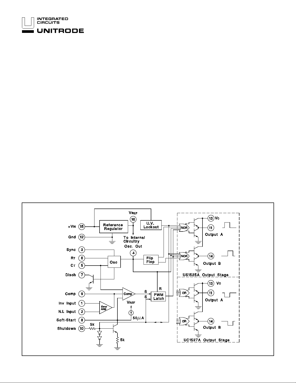
The UC1525A/1527A series of pulse width modulator integrated circuits are designed to offer improved performance and lowered external parts count when used
in designing all types of switching power supplies. The on-chip +5.1V reference is
trimmed to ±1% and the input common-mode range of the error amplifier includ es
the reference voltage, eliminating external resistors. A sync input to the oscillator
allows multiple units to be slaved or a single unit to be synchronized to an external
system clock. A single resistor between the CT and the discharge terminals provides a wide range of dead-time adjustment. These devices also feature built-in
soft-start circuitry with only an external timing ca pacitor r equired. A shutdo wn term inal controls both the soft-star t circuitry and the output stages, providing instantan eous turn off through the PWM latch with pulsed shutdown, as well as soft-start
recycle with longer shutdown commands. These functions are also controlled by
an undervoltage lockout which keeps the outputs off and the soft-start capacitor
discharged for sub-normal input voltages. This lockout circuitry includes approximately 500mV of hysteresis for jitter- free operat ion. Another f eatur e of thes e P WM
circuits is a latch following the comparator. Once a PWM pulse has been terminated for any reason, the outputs will remain off for the duration of the period. The
latch is reset with each clock pulse. The output stages are totem-pole designs capable of sourcing or sinking in excess of 200mA. The UC1525A output stage features NOR logic, giving a LOW output for an OFF state. The UC1527A utilizes OR
logic which r esu lts in a HIGH out put lev el when OFF.
FEATURES
• 8 to 35V Operation
• 5.1V Reference Trimmed to
±1%
• 100Hz to 500kHz Oscillator
Range
• Separate Oscillator Sync
Terminal
• Adjustable Deadtime Control
• Internal Soft-Start
• Pulse-by-Pulse Shutdown
• Input Undervoltage Lockout
with Hysteresis
UC1525A/27A
UC2525A/27A
UC3525A/27A
• Latching PWM to Prevent
Multiple Pulses
• Dual Source/Sink Output
Drivers
BLOCK DIAGRA M
2/96
ABSOLUTE MAXI MUM RATING S (Note 1)
UC1525A/2 7A
UC2525A/2 7A
UC3525A/2 7A
Supply Voltage, (+VIN) . . . . . . . . . . . . . . . . . . . . . . . . . . . . +40V
Collector Supply Voltage (V
C) . . . . . . . . . . . . . . . . . . . . . . +40V
Logic Inputs . . . . . . . . . . . . . . . . . . . . . . . . . . . . -0. 3V t o +5.5 V
Analog Input s . . . . . . . . . . . . . . . . . . . . . . . . . . . . -0.3V to +V
Output Current , Source or Sink . . . . . . . . . . . . . . . . . . . 500mA
Reference Output Current . . . . . . . . . . . . . . . . . . . . . . . . 50mA
Oscillator Char ging Cur ren t . . . . . . . . . . . . . . . . . . . . . . . . 5mA
Power Dissipation at T
Power Dissipation at T
A = +25°C (Note 2). . . . . . . . . . 1000mW
C = +25°C (Note 2). . . . . . . . . . 2000mW
Operating Junct ion Te mp era ture . . . . . . . . . . . -55°C to +150°C
Storage Temperature Range . . . . . . . . . . . . . . -65°C to +150°C
Lead Tempera tu re (Solderin g, 10 seconds). . . . . . . . . . +300°C
Note 1: Values beyond which dama ge may occur .
Note 2: Consult packaging Section of Da ta book for th erma l
limitations and consider at ions of pac kage .
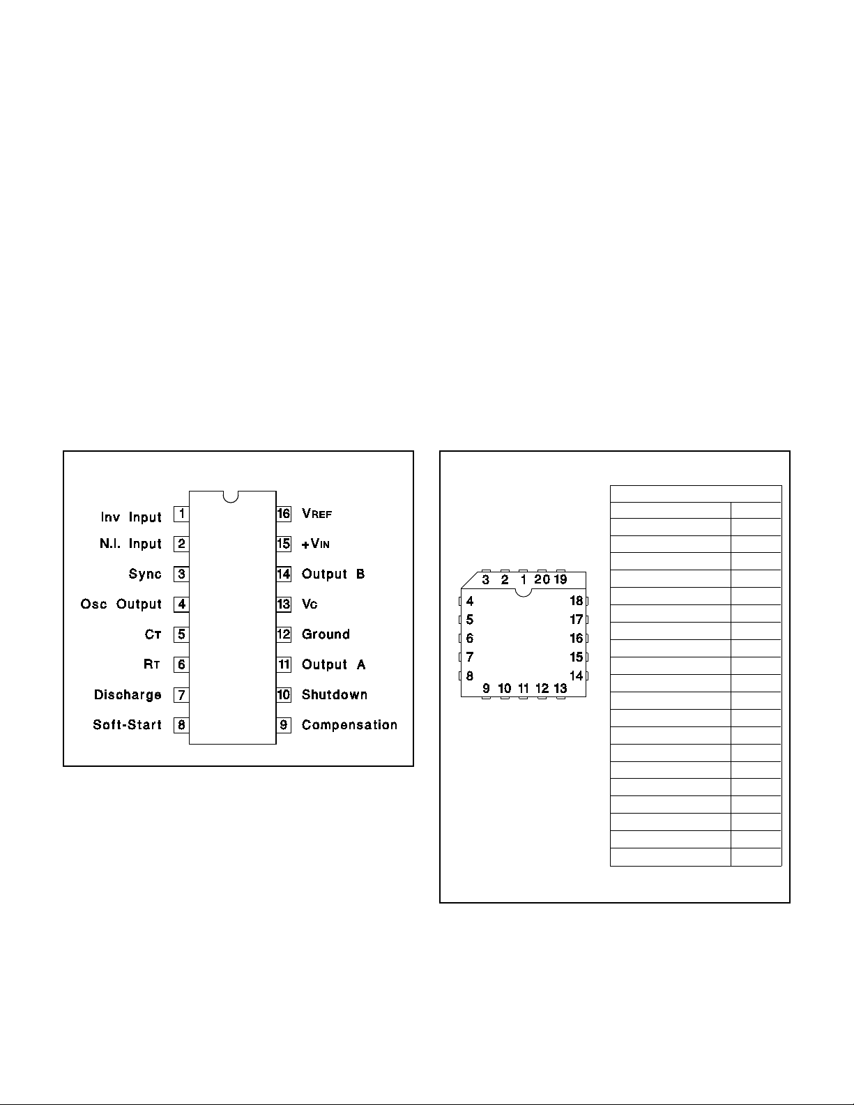
CONNECTION DIAGRAMS
RECOMMENDED OPERAT ING CONDITI ONS
(Note 3)
Input Voltage (+VIN) . . . . . . . . . . . . . . . . . . . . . . . . +8V to +35V
Collector Supply Voltage (V
IN
Sink/Source Load Current (steady state). . . . . . . . 0 to 100mA
Sink/Source Load Current (pe ak). . . . . . . . . . . . . . 0 to 400mA
Referen ce L oa d Curr ent. . . . . . . . . . . . . . . . . . . . . . 0 to 20mA
Oscillator Frequen cy Range. . . . . . . . . . . . . . 100Hz to 400kHz
Oscillator Timing Re sist or. . . . . . . . . . . . . . . . . . . 2kΩ to 150kΩ
Oscillator Timing Ca pacit or. . . . . . . . . . . . . . . . .001µF to 0.1µF
Dead Time Resistor Range . . . . . . . . . . . . . . . . . . . . 0 to 500Ω
Operating Ambient Temperature Range
UC1525A, UC152 7A. . . . . . . . . . . . . . . . . . -55°C to +125°C
UC2525A, UC252 7A. . . . . . . . . . . . . . . . . . . -25°C to +85°C
UC3525A, UC352 7A. . . . . . . . . . . . . . . . . . . . . 0°C to +70°C
Note 3: Range over which the device is functional and
parameter limit s are guar ant ee d.
C) . . . . . . . . . . . . . . +4.5V to +35V
DIL-16 (TOP VIEW)
J or N Package
PLCC-20, LCC- 20 (T OP VIEW)
Q, L Package
PACKAGE PIN FUNCTION
N/C 1
Inv. Input 2
N.I. Input 3
SYNC 4
OSC. output 5
N/C 6
C
R
Discharge 9
Softstart 10
N/C 11
Compensation 12
Shutdown 13
Output A 14
Ground 15
N/C 16
V
Output B 18
+V
V
FUNCTION PIN
T 7
T 8
C 17
IN 19
REF 20
2
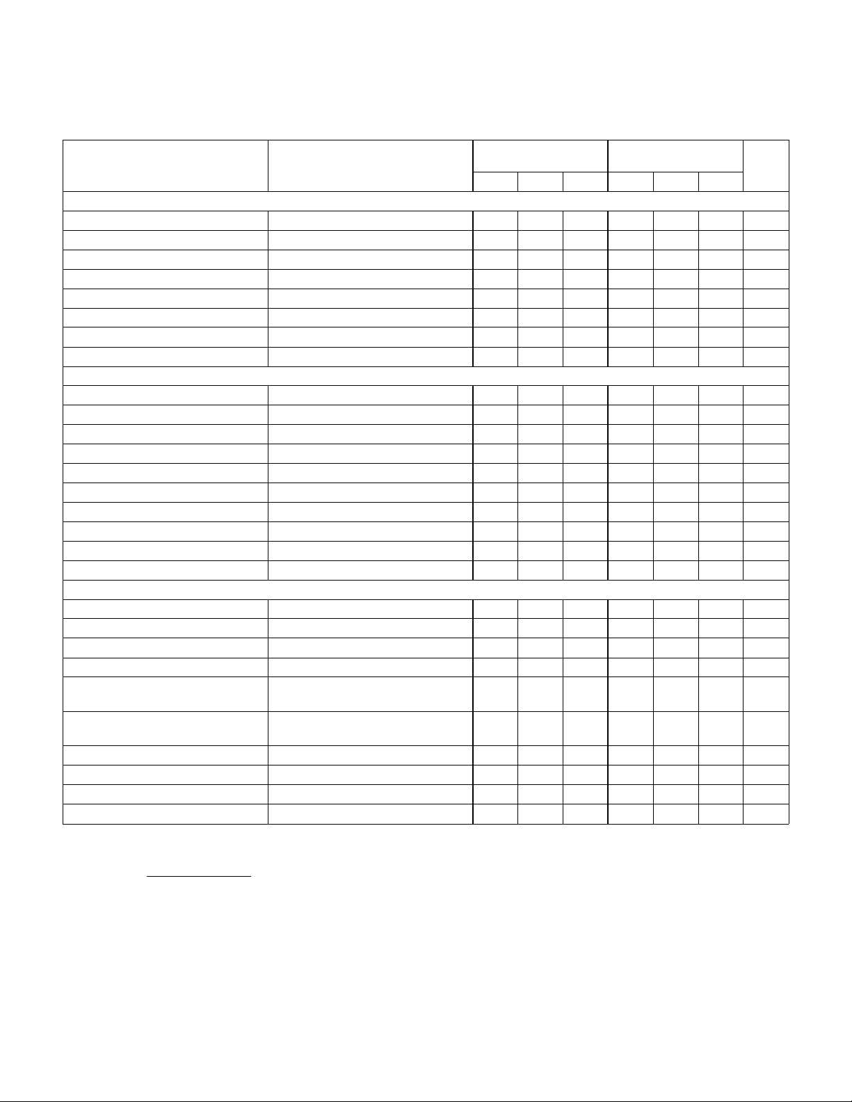
ELECTRICAL CHARACTERISTICS:
UC1525A/2 7A
UC2525A/2 7A
UC3525A/2 7A
+VIN = 20V, and over operating tempera tu re, unless other w ise specified, TA = T J
PARAMETER TEST CONDITIONS
UC1525A/UC2525A
UC1527A/UC2527A
UC3525A
UC3527A
UNITS
MIN TYP MAX MIN TYP MAX
Reference Sec tio n
Output Voltage T
Line Regulation V
Load Regulation I
J = 25°C 5.05 5.10 5.15 5.00 5.10 5.20 V
IN = 8 to 35V 10 20 10 20 mV
L = 0 to 20mA 20 50 20 50 mV
Temperature Stability (Note 5) Over Operating Range 20 50 20 50
Total Output Var iation (Note 5) Line , Load, and Te mp eratu re 5.00 5.20 4.95 5.25 V
Shorter Circuit Curre nt V
Output Noise Voltage (Note 5) 10Hz ≤ 10kHz, T
Long Term Stability (Note 5) T
REF = 0, TJ = 25° C 80 100 80 100 mA
J = 25°C 40 200 40 200 µVrms
J = 125°C 20 50 20 50 mV
Oscillato r Sect ion (Note 6)
Initial Accuracy (Not es 5 & 6) T
Voltage Stability (Notes 5 & 6) V
J = 25°C ± 2 ± 6 ± 2 ± 6%
IN = 8 to 35V ± 0.3 ± 1 ± 1 ± 2%
Temperature Stability (Note 5) Over Operating Range ± 3 ± 6 ± 3 ± 6%
Minimum Frequency R
Maximum Frequency R
Current Mirror I
T = 200kΩΩ, CT = 0.1µµF120120Hz
T = 2kΩΩ, CT = 470pF 400 400 kHz
RT = 2mA 1.7 2.0 2.2 1.7 2.0 2.2 mA
Clock Amplitude (Notes 5 & 6) 3.0 3.5 3.0 3.5 V
Clock Width (Notes 5 & 6) T
J = 25°C 0.3 0.5 1.0 0.3 0.5 1.0 µs
Sync Threshold 1.2 2.0 2.8 1.2 2.0 2.8 V
Sync Input Current Sync Voltage = 3.5V 1.0 2.5 1.0 2.5 mA
Error Amplifier Section (V
CM = 5.1V)
Input Offs et Voltage 0.5 5 2 10 mV
Input Bias Cur ren t 1 10 1 10 µA
Input Offs et Current 1 1 µA
DC Open Loop G ai n R
Gain-Bandwidth Produc t
L ≥≥ 10MΩΩ 60 75 60 75 dB
A
V = 0dB, TJ = 25°C 12 12 MHz
(Note 5)
DC Transconducta nce
J = 25°°C, 30kΩΩ ≤≤ RL ≤≤ 1MΩΩ 1.1 1.5 1.1 1.5 mS
T
(Note s 5 & 7 )
Output Low Le vel 0.2 0.5 0.2 0.5 V
Output High Leve l 3.8 5.6 3.8 5.6 V
Common Mode Rejection V
Supply Voltage Rejection V
CM = 1.5 to 5.2V 60 75 60 75 dB
IN = 8 to 35V 50 60 50 60 dB
Note 5: These parameters, althou gh gua ran te ed ove r the recom m ende d operat ing con dition s, are not 100% teste d in prod uction.
OSC
Note 6: Tested at f
=
f
C
= 40kHz (RT = 3.6kΩ, CT = 0.01µF, RD = 0Ω). Approximate oscillator frequency is defined by:
1
T
(0.7RT
+
3R
D
)
Note 7: DC transconductance (gM) relates to DC open-loop voltag e gain (AV) according to the following equa tion: AV = gMR
where RL is the resistance from pin 9 to ground..
The minimum g
M
specification is used to calculate minimum AV when the error amplifier ou tput is loaded.
3
L

ELECTRICAL CHARACTERISTICS:
UC1525A/27A
UC2525A/27A
UC3525A/27A
+VIN = 20V, and over operating temperat ur e, unless ot he rwise sp ecif ied, TA = TJ
PARAMETER TEST CONDITIONS
UC1525A/UC2525A
UC1527A/UC2527A
UC3525A
UC3527A
UNITS
MIN TYP MAX MIN TYP MAX
PWM Comparator
Minimum Duty-Cycle 0 0 %
Maximum Duty-Cycle 45 49 45 49 %
Input Thresh old (Note 6) Zero Duty-Cycle 0.7 0.9 0.7 0.9 V
Maximum Dut y-Cy c le 3.3 3.6 3.3 3.6 V
Input Bias Curren t (Note 5) .05 1.0 .05 1.0 µA
Shutdown Section
Soft Start Current V
Soft Start Low Level V
Shutdown Thresho ld To outputs, V
Shutdown In put Current V
Shutdown Delay (Note 5) V
Output Drivers (Eac h Out put ) (V
Output Low Le vel I
Output High Leve l I
Under-Voltage Loc kout V
V
C OFF Curren t (Not e 7) VC = 35V 200 200 µA
Rise Time (Note 5) C
Fall Time (Note 5) C
SD = 0V, VSS = 0V 25 50 80 25 50 80 µA
SD = 2.5V 0.4 0.7 0.4 0.7 V
SS = 5.1V, TJ = 25°C 0.6 0.8 1.0 0.6 0.8 1.0 V
SD = 2.5V 0.4 1.0 0.4 1.0 mA
SD = 2.5V, TJ = 25°C 0.2 0.5 0.2 0.5 µs
C = 20V)
SINK = 20 mA 0.2 0.4 0.2 0.4 V
I
SINK
= 100mA 1.0 2.0 1.0 2.0 V
SOURCE = 20mA 1819 1819 V
I
SOURCE = 100mA 17 18 17 18 V
COMP and VSS = High 678678V
L = 1nF, TJ = 25°C 100 600 100 600 ns
L = 1nF, TJ = 25°C 50 300 50 300 ns
Total Standby Current
Supply Current V
IN = 35V 1420 1420mA
Note 5: These parameters, althou gh gua ran te ed ove r the recom m ende d operat ing con dition s, are not 100% teste d in prod uction.
Note 6: Tested at f
= 40kHz (RT = 3.6kΩ, CT = 0.01µF, RD = 0
Ω).
OSC
Note 7: Collector off-state quiescent current measured at pin 13 with outputs low for UC1525A and high for UC1527A.
4

PRINCIPLES OF OPERATI ON AND TYPICAL CHARACTERI ST ICS
UC1525A/2 7A
UC2525A/2 7A
UC3525A/2 7A
UC1525A Output Circuit
(1/2 Circuit Shown)
UC1525A Output Saturation Characteristics
For single-ended su pplies, the drive r outpu ts are
grounded . The V
totem-pole sou rce transist or s on alter nate osc illator cycles.
The low source impeda nce of the out pu t driver s provides
rapid charging of power FET Input capac itance while
minimizing external compon ents.
C terminal is switched to ground by the
In conventional push- pull bipolar designs , forward base
drive is controlled by R1-R3. Rapid turn -of f times for the
power devices are achieved with speed- up cap acit ors
C1 and C2.
Low power transf orm ers can be driven by the UC1525A.
Automatic reset occurs during de ad t ime, when both
ends of the primary winding ar e switc hed to ground .
5

UC1525A/27A
UC2525A/27A
UC3525A/27A
UC1525A Oscillator Schematic
PRINCIPLES OF OPERATION AND TYPICAL CHARACTERISTIC SHUTDO WN OPT IONS
(See Block Diagram)
Since both the compensation and soft-start terminals
(Pins 9 and 8) have current source pull-ups, either can
readily accept a pull-down signal which only has to sink a
maximum of 100µA to turn off the outputs. This is subject
to the added requi rement of disch arging whate ver external capacitance may be attached to these pins.
An alternate approach is the use of the shutdown circuitry
of Pin 10 whi ch ha s been improved to enhance the available shutdown options. Activa ting th is circui t by appl yi ng
Oscillator Charge Time
vs R
T and CT
a positive signal on Pin 10 performs two functions; the
PWM latch is immedi ately set providing the fastest turnoff signal to the outputs; and a 150µA-current sink begins
to discharge the external soft-star t capacitor. If the shutdown command is short, the PWM signal is terminated
without significant discharge of the soft-start capacitor,
thus, allowing, for example, a convenient implementation
of pulse-by-pulse current limiting. Holding Pin 10 high for
a longe r duration, however, will ultimately discharge this
external capacitor , recycling slow turn-on upon release.
Pin 10 should not be left floating as noise pickup could
conceivably interrupt normal operation.
Oscillator Disch arge Time
vs R
D and CT
6

UC1525A/27A
UC2525A/27A
UC3525A/27A
Maximum Value RD vs Minimum Value RT
LAB TEST FIXTURE
Error Amplif ier Voltage Gain
and Phase vs Frequency
RL is impedance from pin 9 to ground. Values below
30kΩΩ will begin to limit the maximum duty cy cle.
UNITRODE INTEGRATED CIRCUITS
7 CONTINENTAL BLVD. •• MERRIMACK, NH 03054
TEL. (603) 424-2410 • FAX (603) 424-3460
7

IMPORTANT NOTICE
T exas Instruments and its subsidiaries (TI) reserve the right to make changes to their products or to discontinue
any product or service without notice, and advise customers to obtain the latest version of relevant information
to verify, before placing orders, that information being relied on is current and complete. All products are sold
subject to the terms and conditions of sale supplied at the time of order acknowledgement, including those
pertaining to warranty, patent infringement, and limitation of liability.
TI warrants performance of its semiconductor products to the specifications applicable at the time of sale in
accordance with TI’s standard warranty. Testing and other quality control techniques are utilized to the extent
TI deems necessary to support this warranty . Specific testing of all parameters of each device is not necessarily
performed, except those mandated by government requirements.
CERTAIN APPLICATIONS USING SEMICONDUCT OR PRODUCTS MAY INVOLVE POTENTIAL RISKS OF
DEATH, PERSONAL INJURY, OR SEVERE PROPERTY OR ENVIRONMENTAL DAMAGE (“CRITICAL
APPLICATIONS”). TI SEMICONDUCTOR PRODUCTS ARE NOT DESIGNED, AUTHORIZED, OR
WARRANTED TO BE SUITABLE FOR USE IN LIFE-SUPPORT DEVICES OR SYSTEMS OR OTHER
CRITICAL APPLICA TIONS. INCLUSION OF TI PRODUCTS IN SUCH APPLICATIONS IS UNDERST OOD TO
BE FULLY AT THE CUSTOMER’S RISK.
In order to minimize risks associated with the customer’s applications, adequate design and operating
safeguards must be provided by the customer to minimize inherent or procedural hazards.
TI assumes no liability for applications assistance or customer product design. TI does not warrant or represent
that any license, either express or implied, is granted under any patent right, copyright, mask work right, or other
intellectual property right of TI covering or relating to any combination, machine, or process in which such
semiconductor products or services might be or are used. TI’s publication of information regarding any third
party’s products or services does not constitute TI’s approval, warranty or endorsement thereof.
Copyright 1999, Texas Instruments Incorporated
 Loading...