

Advanced Regulating Pulse Width Modulators
UC1524
UC2524
UC3524
FEATURES
Complete PWM Power Control
•
Circuitry
Uncommitted Outputs for
•
Single-ended or Push-pull
Applications
Low Standby Current…8mA Typical
•
Interchangeable with SG1524,
•
SG2524 and SG3524, Respectively
DESCRIPTION
The UC1524, UC2524 and UC3524 incorporate on a single monolithic chip
all the functions required for the construction of regulating power supplies, in
verters or switching regulators. They can also be used as the control element
for high-power-output applications. The UC1524 family was designed for
switching regulators of either polarity, transformer-coupled dc-to-dc convert
ers, transformerless voltage doublers and polarity converter applications em
ploying fixed-frequency, pulse-width modulation techniques. The dual
alternating outputs allow either single-ended or push-pull applications. Each
device includes an on-chip reference, error amplifier, programmable oscilla
tor, pulse-steering flip-flop, two uncommitted output transistors, a high-gain
comparator, and current-limiting and shut-down circuitry. The UC1524 is
characterized for operation over the full military temperature range of -55°C
to +125°C. The UC2524 and UC3524 are designed for operation from -25°C
to +85°C and 0° to +70°C, respectively.
-
-
-
-
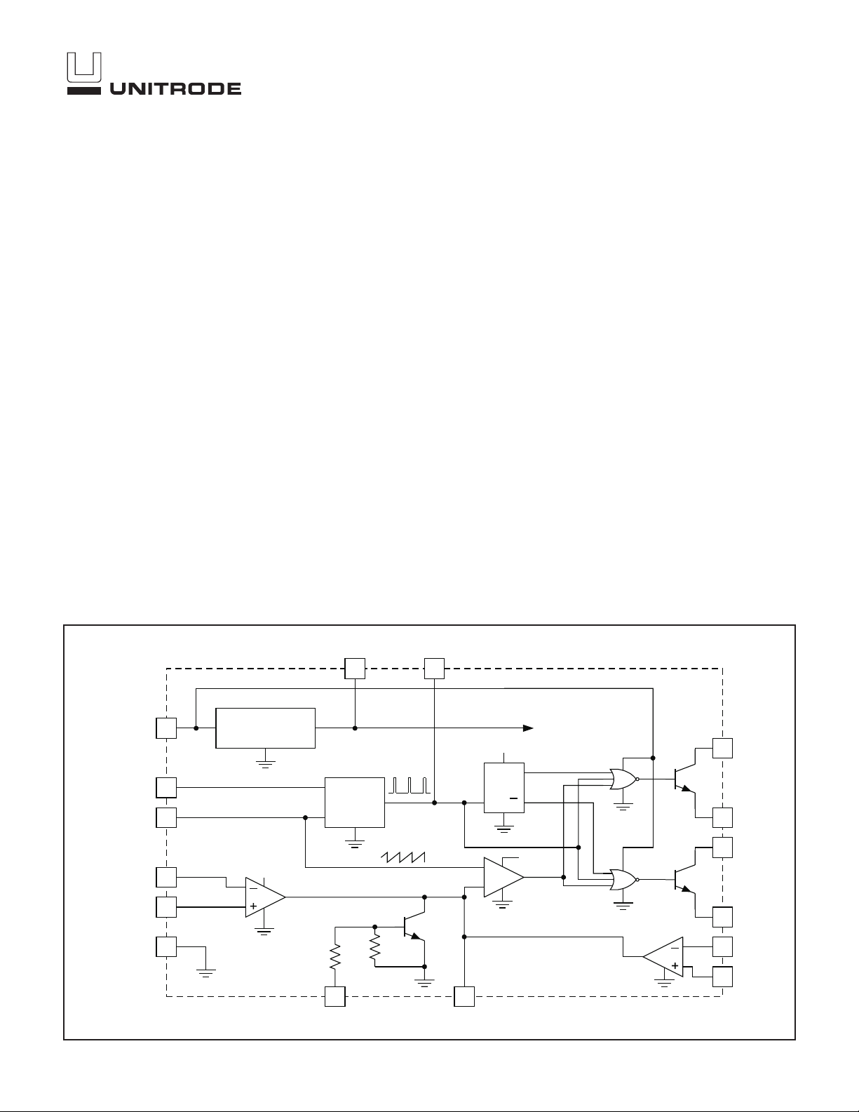
BLOCK DIAGRAM
15
V
IN
6
R
T
7
C
T
(RAMP)
INV INPUT
NI INPUT
GROUND
(SUBSTRATE)
1
2
8
REFERENCE
REGULATOR
+5V
EA
10
V
REF
16
OSC
1k
OSC OUT
COMPARATOR
10k
3
+5V TO ALL
INTERNAL
Q
QR
CIRCUITRY
+5V
CL
11
13
14
5
4
C
A
E
A
C
B
E
B
–SENSE
+SENSE
+5V 12
9
SLUS180A - NOVEMBER 1999
SHUTDOWN
COMPENSATION
ABSOLUTE MAXIMUM RATINGS (Note 1)
Supply Voltage, VCC(Notes 2 and 3) . . . . . . . . . . . . . . . . . 40V
Collector Output Current. . . . . . . . . . . . . . . . . . . . . . . . . 100mA
Reference Output Current . . . . . . . . . . . . . . . . . . . . . . . . 50mA
Current Through C
Power Dissipation at T
Power Dissipation at T
Terminal . . . . . . . . . . . . . . . . . . . . . . –5mA
T
= +25°C (Note 4). . . . . . . . . . 1000mW
A
= +25°C (Note 4). . . . . . . . . . 2000mW
C
Operating Junction Temperature Range . . . . –55°C to +150°C
Storage Temperature Range . . . . . . . . . . . . . –65°C to +150°C
Note 1: Over operating free-air temperature range unless oth
erwise noted.
Note 2: All voltage values are with respect to the ground termi
nal, pin 8.
Note 3: The reference regulator may be bypassed for opera
tion from a fixed 5V supply by connecting the V
CC
-
and
reference output pins both to the supply voltage. In this
configuration the maximum supply voltage is 6V.
Note 4: Consult packaging section of databook for thermal lim
itations and considerations of package.
RECOMMENDED OPERATING CONDITIONS
Supply Voltage, VCC. . . . . . . . . . . . . . . . . . . . . . . . . . 8V to 40V
Reference Output Current . . . . . . . . . . . . . . . . . . . . . 0 to 20mA
Current through C
Timing Resistor, R
Timing Capacitor, C
Operating Ambient Temperature Range
UC1524 . . . . . . . . . . . . . . . . . . . . . . . . . . . . –55°C to +125°C
UC2524 . . . . . . . . . . . . . . . . . . . . . . . . . . . . . –25°C to +85°C
UC3524 . . . . . . . . . . . . . . . . . . . . . . . . . . . . . . . 0°C to +70°C
Terminal . . . . . . . . . . . . . –0.03mA to –2mA
T
. . . . . . . . . . . . . . . . . . . . . 1.8kΩ to 100kΩ
T
. . . . . . . . . . . . . . . . . . . 0.001µF to 0.1µF
T
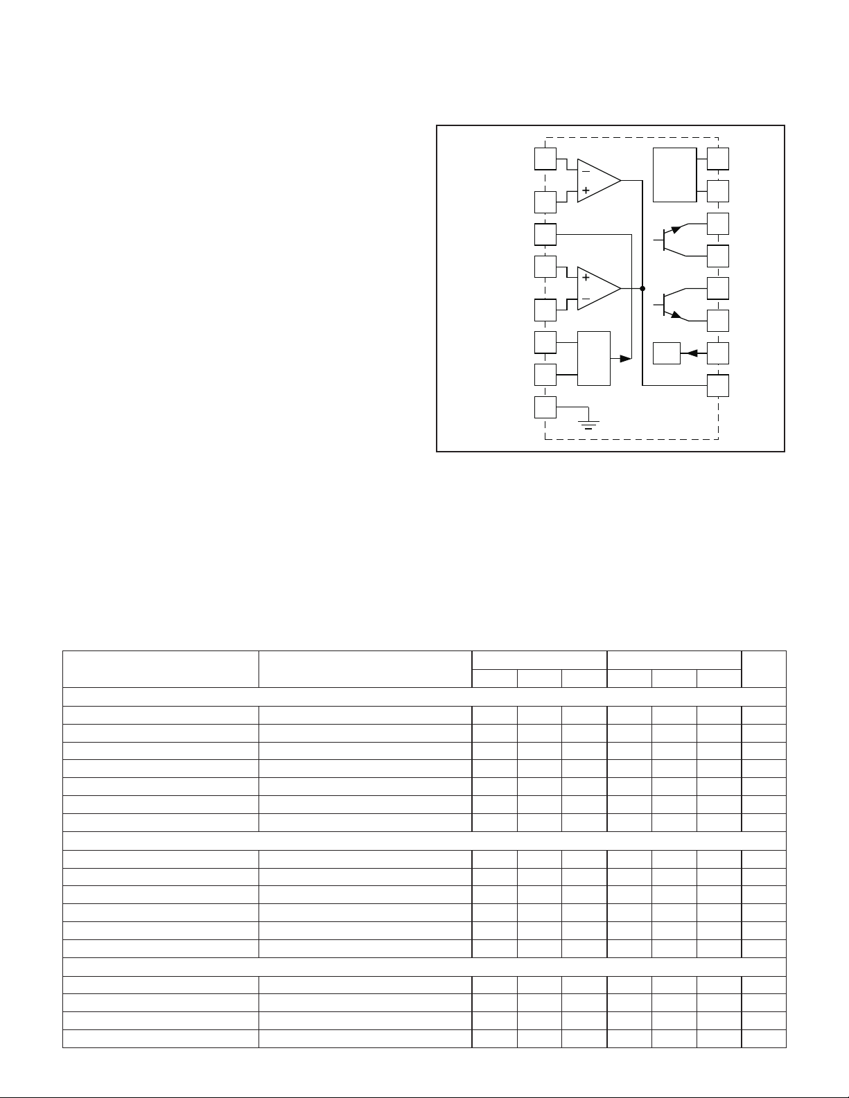
CONNECTION DIAGRAM
INV INPUT
NON INV
INPUT
OSC OUT
-
-
-
CLSENSE(+)
CLSENSE (–-)
R
C
GND
T
T
UC1524
UC2524
UC3524
1
EA
2
3
4
CL
5
6
OSC
7
8
REF
REG
S/D
16
15
14
13
12
11
10
V
REF
V
IN
E
B
C
B
C
A
E
A
S/D
9
COMP
ELECTRICAL CHARACTERISTICS: Unless otherwise stated, these specifications apply for T
for the UC1524, –25°C to +85°C for the UC2524, and 0°C to +70°C for the UC3524, V
T
A=TJ
.
= 20V, and f = 20kHz,
IN
= –55°C to +125°C
A
UC1524/UC2524 UC3524 UNITS
PARAMETER TEST CONDITIONS
MIN MAX MIN MAX
Reference Section
Output Voltage 4.8 5.0 5.2 4.6 5.0 5.4 V
Line Regulation V
Load Regulation I
Ripple Rejection f = 120Hz, T
Short Circuit Current Limit V
IN = 8 to 40V 10 20 10 30 mV
L = 0 to 20mA 20 50 20 50 mV
J = 25°C 66 66 dB
REF = 0, TJ = 25°C 100 100 mA
Temperature Stability Over Operating Temperature Range 0.3 1 0.3 1 %
Long Term Stability T
J = 125°C, t = 1000 Hrs. 20 20 mV
Oscillator Section
Maximum Frequency C
Initial Accuracy R
Voltage Stability V
= .001mfd, RT= 2kΩ 300 300 kHz
T
and CTConstant 5 5 %
T
= 8 to 40V, TJ= 25°C 1 1 %
IN
Temperature Stability Over Operating Temperature Range 5 5 %
Output Amplitude Pin 3, T
Output Pulse Width C
T
= 25°C 3.5 3.5 V
J
= .01mfd, TJ= 25°C 0.5 0.5
Error Amplifier Section
Input Offset Voltage V
Input Bias Current V
= 2.5V 0.5 5 2 10 mV
CM
= 2.5V 2 10 2 10
CM
Open Loop Voltage Gain 72 80 60 80 dB
Common Mode Voltage T
= 25°C 1.8 3.4 1.8 3.4 V
J
2
µs
µA

UC1524
UC2524
UC3524
ELECTRICAL CHARACTERISTICS: Unless otherwise stated, these specifications apply for T
for the UC1524, –25°C to +85°C for the UC2524, and 0°C to +70°C for the UC3524, V
T
Note: Excluding oscillator charging current, error and current limit dividers, and with outputs open.
.
A=TJ
PARAMETER TEST CONDITIONS
Error Amplifier Section (cont.)
Common Mode Rejection Ratio T
Small Signal Bandwidth A
Output Voltage T
Comparator Section
Duty-Cycle % Each Output On 0 45 0 45 %
Input Threshold Zero Duty-Cycle 1 1 V
Input Bias Current 1 1
Current Limiting Section
Sense Voltage Pin 9 = 2V with Error Amplifier
Sense Voltage T.C. 0.2 0.2 mV/°C
Common Mode Voltage –1 +1 –1 +1 V
Output Section (Each Output)
Collector-Emitter Voltage 40 40 V
Collector Leakage Current V
Saturation Voltage I
Emitter Output Voltage V
Rise Time R
Fall Time R
Total Standby Current (Note)
= 25°C 70 70 dB
J
V = 0dB, T
= 25°C 0.5 3.8 0.5 3.8 V
J
Maximum Duty-Cycle 3.5 3.5 V
Set for Maximum Out, T
= 40V 0.1 50 0.1 50
CE
C = 50mA 1 2 1 2 V
= 20V 17 18 17 18 V
IN
C = 2kΩ,T
C = 2kΩ,T
V
= 40V 8 10 8 10 mA
IN
= 25°C 3 3 MHz
J
= 25°C
J
= 25°C 0.2 0.2
J
= 25°C 0.1 0.1
J
UC1524/UC2524 UC3524 UNITS
MIN MAX MIN MAX
190 200 210 180 200 220 mV
= 20V, and f = 20kHz,
IN
= –55°C to +125°C
A
µA
µA
µs
µs
PRINCIPLES OF OPERATION
The UC1524 is a fixed-frequency pulse-width-modulation
voltage regulator control circuit. The regulator operates at
a frequency that is programmed by one timing resistor
), and one timing capacitor (CT), RTestablishes a
(R
T
constant charging current for C
voltage ramp at C
, which is fed to the comparator pro
T
viding linear control of the output pulse width by the error
amplifier. The UC1524 contains an on-board 5V regulator
that serves as a reference as well as powering the
UC1524’s internal control circuitry and is also useful in
supplying external support functions. This reference volt
age is lowered externally by a resistor divider to provide a
reference within the common-mode range of the error
amplifier or an external reference may be used. The
power supply output is sensed by a second resistor di
vider network to generate a feedback signal to the error
amplifier. The amplifier output voltage is then compared
to the linear voltage ramp at C
pulse out of the high-gain comparator is then steered to
. This results in a linear
T
. The resulting modulated
T
the appropriate output pass transistor (Q
1 or Q2)bythe
pulse-steering flip-flop, which is synchronously toggled by
the oscillator output. The oscillator output pulse also
serves as a blanking pulse to assure both outputs are
never on simultaneously during the transition times. The
-
width of the blanking pulse is controlled by the valve of
. The outputs may be applied in a push-pull configura
C
T
tion in which their frequency is half that of the base oscil
lator, or paralleled for single-ended applications in which
the frequency is equal to that of the oscillator. The output
-
of the error amplifier shares a common input to the com
parator with the current limiting and shutdown circuitry
and can be overridden by signals from either of these in
puts. This common point is also available externally and
-
may be employed to control the gain of, or to compen
sate, the error amplifier or to provide additional control to
the regulator.
3
-
-
-
-
-

TYPICAL CHARACTERISTICS
UC1524
UC2524
UC3524
Open-loop voltage amplification of error amplifier vs
frequency.
Oscillator frequency vs timing components.
Output saturation voltage vs load current.Output dead time vs timing capacitance value.
4

APPLICATION INFORMATION
Oscillator
UC1524
UC2524
UC3524
Synchronous Operation
The oscillator controls the frequency of the UC1524 and is
programmed by R
and CTaccording to the approximate
T
formula:
1.18
f
′
RC
TT
where RTis in kΩ
where C
is in mF
T
where f is in kHz
Practical values of C
Practical values of R
fall between 0.001mF and 0.1mF.
T
fall between 1.8kΩ and 100kΩ.
T
This results in a frequency range typically from 120Hz to
500kHz.
Blanking
The output pulse of the oscillator is used as a blanking
pulse at the output. This pulse width is controlled by the
value of C
. If small values of CTare required for fre-
T
quency control, the oscillator output pulse width may still
be increased by applying a shunt capacitance of up to
100pF from pin 3 to ground. If still greater dead-time is
required, it should be accomplished by limiting the maximum duty cycle by clamping the output of the error amplifier. This can easily be done with the circuit in Figure 1:
When an external clock is desired, a clock pulse of ap
proximately 3V can be applied directly to the oscillator
output terminal. The impedance to ground at this point is
approximately 2kΩ. In this configuration R
TCT
must be
selected for a clock period slightly greater than that of the
external clock.
If two or more UC1524 regulators are to operated synchro
nously, all oscillator output terminals should be tied to
gether, all C
terminals connected to single timing
T
capacitor, and the timing resistor connected to a single R
terminal. The other R
to V
the C
. Minimum lead lengths should be used between
REF
terminals.
T
V
COMP 5k9
GND
terminals can be left open or shorted
T
16
REF
1N916
8
Figure 1. Error amplifier clamp.
-
-
-
,
T
Figure 2. Single-ended LC switching regulator circuit.
5

UC1524
UC2524
UC3524
Figure 3. Push-pull transformer coupled circuit.
Figure 4. Open loop test circuit.
UNITRODE CORPORATION
7 CONTINENTAL BLVD. • MERRIMACK, NH 03054
TEL. (603) 424-2410 FAX (603) 424-3460
6
 Loading...