

UC1907
UC2907
UC3907
DESCRIPTION
The UC3907 family of Load Share Controller ICs provides all the necessary
features to allow multiple independent power modules to be paralleled such
that each module supplies only its proportionate share to total load current.
This sharing is accomplished by controlling each module’s power stage
with a command generated from a voltage feedback amplifier whose reference can be independently adjusted in response to a common share bus
voltage.By monitoring the current from each module, the current share bus
circuitry determines which paralleled module would normally have the highest output current and, with the designation of this unit as the master, adjusts all the other modules to increase their output current to within 2.5% of
that of the master.
The current share bus signal interconnecting all the paralleled modules is a
low-impedance, noise-insensitive line which will not interfere with allowing
each module to act independently should the bus become open or shorted
to ground. The UC3907 controller will reside on the output side of each
power module and its overall function is to supply a voltage feedback loop.
The specific architecture of the power stage is unimportant. Either switching or linear designs may be utilized and the control signal may be either directly coupled or isolated though the use of an opto coupler or other
isolated medium.
Other features of the UC3907 include 1.25% accurate reference: a
low-loss, fixed gain current sense amplifier, a fully differential,
high-impedance voltage sensing capability, and a status indicator to designate which module is performing as master.
Load Share Controller
FEATURES
Fully Differential High Impedance
Voltage Sensing
Accurate Current Amplifier for Precise
Current Sharing
Opto Coupler Driving Capability
1.25% Trimmed Reference
Master Status Indication
4.5V TO 35V Operation
SLUS165 - MARCH 1999
11
14
10
13
8
9
12
15
16
7
5
4
1
6
3
2
2k
2k
+
–
40k
40k
CURRENT SENSE
AMPLIFIER
100
+
–
BUFFER
AMPLIFIER
10k
+
–
+
50mV
ADJUST
AMPLIFIER
ADJ
17.5k
V
CC
1k
V
REF
1.750V
+
–
+
GROUND
AMPLIFIER
0.25V
GND
+
–
50k
20k
+
1.0V
1.75V
VOLTAGEERROR AMPLIFIER
ST ATUSINDICATE
CURRENT SHARE BUS
ADJ INPUT
ADJ OUT
ISET
OPTO DRIVE
COMP
(+) SENSE
VCC (4.5V TO35V)
(–) SENSE
POWER RTN
ARTIFICIAL GND
VREF
C/S OUT
C/S (–)
C/S (+)
DRIVE
AMPLIFIER
+
–
DRV
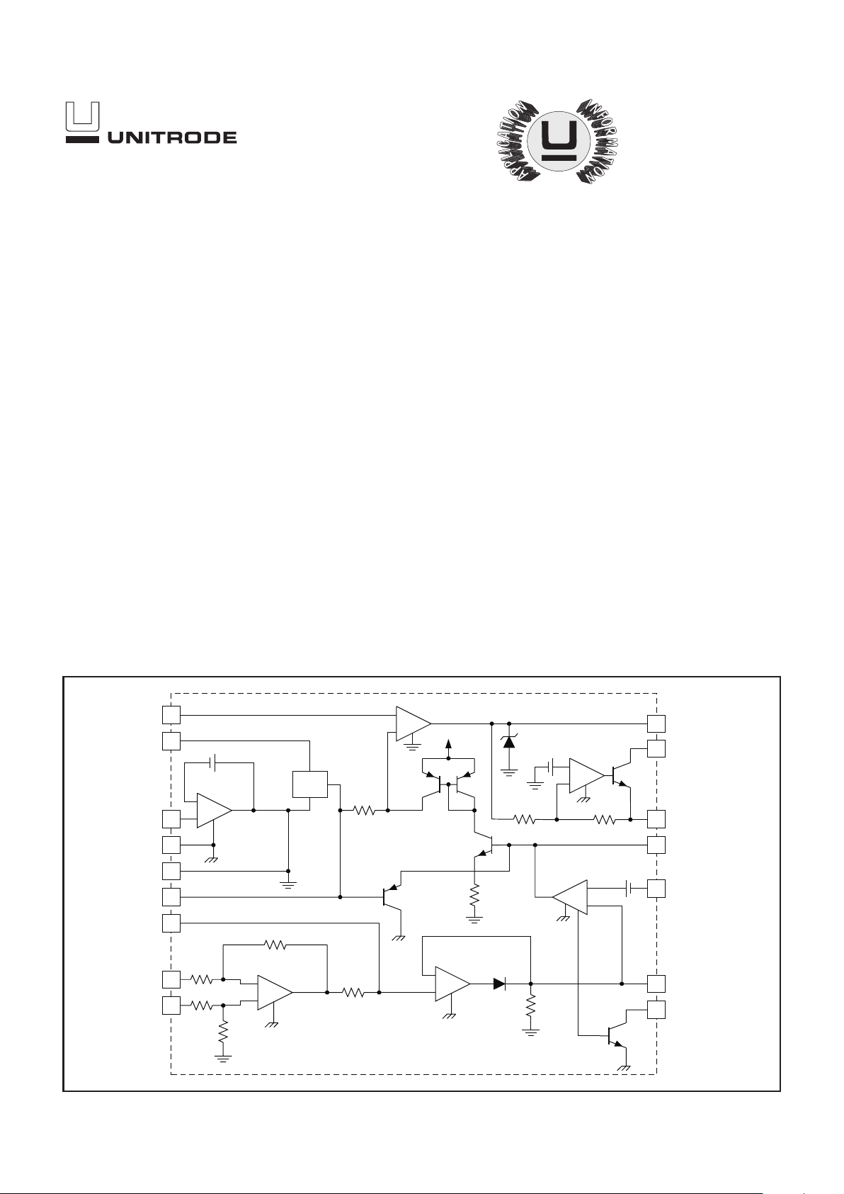
BLOCK DIAGRAM
UDG-99052
2
UC1907
UC2907
UC3907
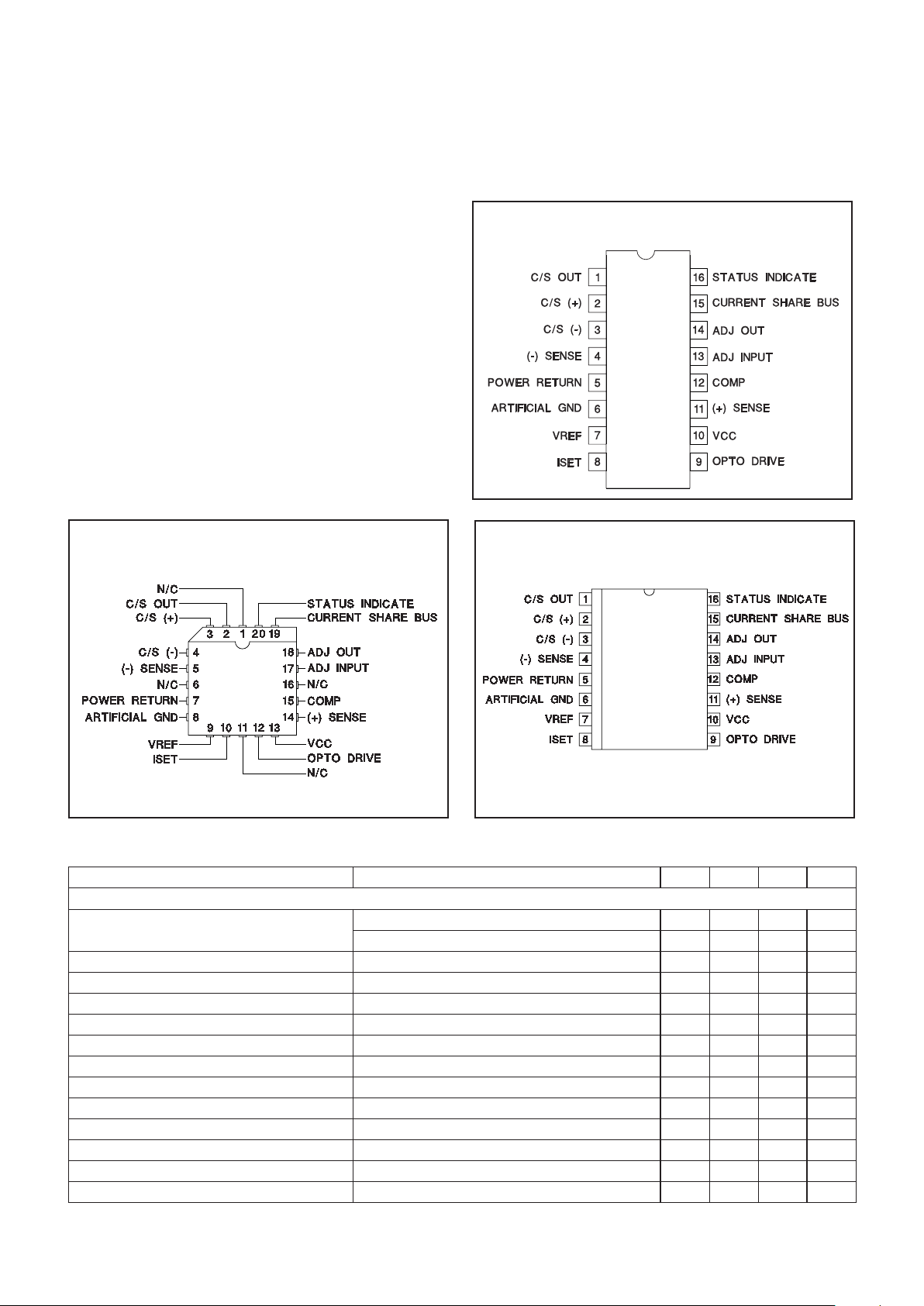
DIL-16 (Top View)
J or N Package
ABSOLUTE MAXIMUM RATINGS
Supply Voltage . . . . . . . . . . . . . . . . . . . . . . . . . . . . . . . . . +35V
Opto Out Voltage. . . . . . . . . . . . . . . . . . . . . . . . . . . . . . . . +35V
Opto Out Current . . . . . . . . . . . . . . . . . . . . . . . . . . . . . . +20mA
Status Indicate Sink Current. . . . . . . . . . . . . . . . . . . . . . +20mA
C/S Input Voltage . . . . . . . . . . . . . . . . . . . . . . . . . . . . . . . +35V
Share Bus Voltage. . . . . . . . . . . . . . . . . . . . . . . – 0.3V to +35V
Other Analog Inputs and Outputs (Zener clamped)
Maximum Forced Voltage . . . . . . . . . . . . . . . – 0.3V to +10V
Maximum Forced Current. . . . . . . . . . . . . . . . . . . . . . ±10mA
Ground Amp Sink Current . . . . . . . . . . . . . . . . . . . . . . . +50mA
Pins 1, 9, 12, 15 Sink Current. . . . . . . . . . . . . . . . . . . . . +20mA
Storage Temperature Range. . . . . . . . . . . . . – 65°C to +150°C
Junction Temperature . . . . . . . . . . . . . . . . . . – 55°C to +150°C
Lead Temperature (Solder 10 Seconds) . . . . . . . . . . . . +300°C
Pin Nos. refer to 16 Pin DIL Package
Currents are positive into, negative out of the specified
terminal. Consult packaging section of databook for thermal
limitations and considerations of package.
CONNECTION DIAGRAMS
ELECTRICAL CHARACTERISTICS:
Unless otherwise stated these specifications apply for TA= –55°C to +125°C for
UC1907; –40°C to +85°C for UC2907; and 0°C to +70°C for UC3907; VIN= 15V, TA=TJ.
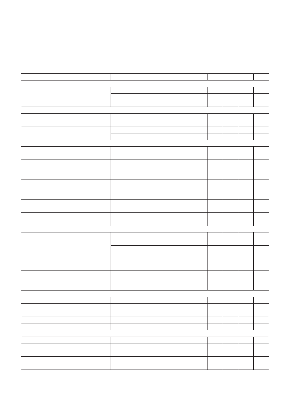
PARAMETER TEST CONDITIONS
MIN TYP MAX UNITS
Voltage Amp Section
Input Voltage COMP = 1V, T
A
= 25°C 1.975 2.000 2.025 V
COMP = 1V, Over Temp 1.960 2.000 2.040 V
Line Regulation V
IN
= 4.5V to 35V 15 mV
Load Regulation I
L
Reference = 0.0mA to – 10mA 10 mV
Long Term Stability T
A
= 125°C, 1000hrs (Note 2) 5 25 mV
Total Output Variation Line, Load, Temp 1.960 2.040
Input Adjust Range ADJ OUT from max high to max low 85 100 115 mV
Input Bias Current –1 µA
Open Loop Gain COMP = 0.75V to 1.5V 65 dB
Unity Gain Bandwidth T
A
= 25°C (Note 2) 700 kHz
Output Sink Current (+) SENSE = 2.2V, COMP = 1V 6 15 mA
Output Source Current (+) SENSE = 1.8V, COMP = 1V 400 600 µA
V
OUT
High (+) SENSE = 1.8V, IL= – 400µa 1.85 2 V
V
OUT
Low (+) SENSE = 2.2V, IL= +1mA 0.15 0.40 V
PLCC–20, LCC–20 (Top View)
Q PACKAGE, L PACKAGE
SOIC-16 (Top View)
DW Package
3
UC1907
UC2907
UC3907
ELECTRICAL CHARACTERISTICS:
Unless otherwise stated these specifications apply for TA= –55°C to +125°C for
UC1907; –40°C to +85°C for UC2907; and 0°C to +70°C for UC3907; VIN= 15V, TA=TJ.
PARAMETER TEST CONDITIONS
MIN TYP MAX UNITS
Reference Section
Output Voltage T
A
= 25°C 1.970 2.000 2.030 V
Over Operating Temp 1.955 2.000 2.045 V
Short Circuit Current VREF = 0.0V – 15 – 30 – 60 mA
Ground Amp Section
Output Voltage 200 250 300 mV
Common Mode Variation (–) SENSE from 0.0V to 2V 5 mV
Load Regulation I
L
= 0.0mA to 20mA, TA= 25°C 10 mV
I
L
= 0.0mA to 20mA, Over Temp 15 mV
Adjust Amp Section
Input Offset Voltage ADJ OUT = 1.5V, Vcm = 0.0V 40 50 60 mV
Input Bias Current – 2 µA
Open Loop Gain 1.5V≤ADJ OUT≤ 2.25V 65 dB
Unity Gain Bandwidth T
A
= 25°C, C
OUT
=1µF (Note 2) 500 Hz
Transconductance I
OUT
= – 10µA to +10µA, V
OUT
= 1.5V 1.7 3 4.5 ms
Output Sink Current Vid = 0.0V, ADJ OUT = 1.5V 55 135 225 µA
Output Source Current Vid = 250mV, ADJ OUT = 1.5V 110 200 350 µA
V
OUT
High Vid = 250mV, I
OUT
= – 50µA 2.20 2.70 2.90 V
V
OUT
Low Vid = 0.0V, I
OUT
= 50µA 0.75 1.15 V
Common Mode Rejection Ratio Vcm = 0.0 to 10V 70 dB
Output Gain to V/A V
OUT
ADJ OUT = 1.5V to 2V 50 57 64 mV/V
∆(+) SENSE/ ∆ADJ OUT
Current Amp Section
Gain Vcm = 0.0V, Vid = 50mV to 100mV 19.2 19.6 20.1 V/V
Output Voltage Vc/s (+) = Vc/s (–) = 0.0V, T
A
= 25°C 210 250 290 mV
Vc/s (+) = Vc/s (–) = 0.0V, Over Temp 180 250 330 mV
Input Offset Change with Common Mode
Input
Vcm = 0V to 13V 600 µV/V
V
OUT
High Vid = 1V 10 14.5 V
V
OUT
Low Vid = – 1V, IL= 1mA 350 450 mV
Power Supply Rejection Ratio V
IN
= 4.5V to 35V, Vcm = 0.0V 60 dB
Slew Rate 0.4 V/µs
Drive Amp Section Rset = 500Ω to Artificial Gnd, Opto Drive = 15V
Voltage Gain COMP = 0.5V to 1V 2.3 2.5 2.6 V/V
I
SETVOUT
High (+) SENSE = 2.2V 3.8 4.1 4.4 V
I
SETVOUT
Low (+) SENSE = 1.8V 270 300 mV
Opto out Voltage Range 435V
Zero Current Input Threshold 1.55 1.65 1.75 V
Buffer Amp Section
Input Offset Voltage Input = 1V 5 mV
Output Off Impedance Input = 1V, Output = 1.5V to 2V 5 10 20 kΩ
Output Source Current Input = 1V, Output = 0.5V 6 15 mA
Common Mode Rejection Ratio Vcm = 0.3V to 10V 70 dB
Power Supply Rejection Ratio V
IN
= 4.5V to 35V 70 dB

4
UC1907
UC2907
UC3907
ELECTRICAL CHARACTERISTICS:
Unless otherwise stated these specifications apply for TA= –55°C to +125°C for
UC1907; –40°C to +85°C for UC2907; and 0°C to +70°C for UC3907; VIN= 15V, TA=TJ.
PARAMETER TEST CONDITIONS
MIN TYP MAX UNITS
Under Voltage Lockout Section
Startup Threshold 3.7 4.4 V
Threshold Hysteresis 20 mV
Status Indicate Section
V
OUT
Low ADJ OUT = Current Share Bus 0.2 0.5 V
Output Leakage ADJ OUT = 1V, V
OUT
= 35V 0.1 5 µA
Total Stand by Current Section
Startup Current VIN= UVLO – 0.2V 3 5 mA
Operating Current V
IN
= 35V 6 10 mA
Note 1: Unless otherwise specified all voltages are with respect to (–) SENSE. Currents are positive into, negative out of the
specified terminal.
Note 2: Guaranteed by design. Not 100% tested in production.
(–) SENSE (Pin 4) - This is a high-impedance pin intended to allow remote sensing of the system ground,
bypassing any voltage drops which might appear in the
power return line. This point should be considered as
the “true” ground. Unless otherwise stated, all voltages are with respect to this point.
ARTIFICIAL GROUND (Pin 6) - This is a low impedance
circuit ground which is exactly 250 millivolts above the (–)
SENSE terminal. This offset allows the Ground Buffer
Amplifier negative headroom to return all the control bias
and operating currents while maintaining a high impedance at the (–) SENSE input.
POWER RTN (Pin 5) - This should be the most negative
voltage available and can range from zero to 5V below
the (–) SENSE terminal. It should be connected as close
to the power source as possible so that voltage drops
across the return line and current sensing impedances
lie between this terminal and the (–) SENSE point.
VREF (Pin 7) - The internal Voltage Reference is a
band-gap circuit set at 2.0 Volts with respect to the (–)
SENSE input (1.75V above the ARTIFICIAL GROUND),
and an accuracy of ± 1.5%. This circuit, as well as all the
other chip functions, will work over a supply voltage
range of 4.5V to 35V allowing operation from unregulated
DC, an auxiliary voltage, or the same output voltage that
it is controlling. Under voltage lockout has been included
to insure proper startup by disabling internal bias currents until the reference rises into regulation.
VOLTAGE AMPLIFIER (Pins 11, 12) - This circuit is the
feedback control gain stage for the power module’s output voltage regulation, and overall loop compensation will
normally be applied around this amplifier. Its output will
swing from slightly above the ground return to an internal
clamp of 2.0 Volts. The reference trimming is performed
closed loop, and measured at pin 11, (+) SENSE. The
value is trimmed to 2V ±1.25%.
DRIVE AMPLIFIER (Pins 8, 9, 12) - This amplifier is
used as an inverting buffer between the Voltage Amplifier’s output and the medium used to couple the feedback
signal to the power controller. It has a fixed voltage gain
of 2.5 and is usually configured with a current-setting resistor to ground. This establishes a current - sinking output optimized to drive optical couplers biased at any
voltage from 4.5V to 35V, with current levels up to 20mA.
The polarity of this stage is such that an increasing voltage at the Voltage Amplifier’s sense input (as, for example, at turn on) will increase the opto’s current. In a
nonisolated application, a voltage signal ranging from
0.25V to 4.1V may be taken from the current-setting output but it should be noted that this voltage will also increase with increasing sense voltage and an external
inverter may be required to obtain the correct feedback
polarity.
CURRENT AMPLIFIER (Pins 1, 2, 3) - This amplifier has
differential sensing capability for use with an external
shunt in the power return line. The common-mode range
of its input will accommodate the full range between the
Power Return point and VCC–2V which will allow undefined line impedances on either side of the current shunt.
The gain is internally set at 20 giving the user the ability
to establish the maximum voltage drop across the current sense resistor at any value between 50 and 500 millivolts. While the bandwidth of this amplifier may be
reduced with the addition of an external output capacitor
to ground, in most cases this is not required as the compensation of the Adjust Amplifier will typically form the
dominant pole in the adjust loop.
PIN/BLOCK DESCRIPTIONS

5
UC1907
UC2907
UC3907
BUFFER AMPLIFIER (Pins 1, 15) - This amplifier is a
uni-directional buffer which drives the CURRENT SHARE
BUS - the line which will interconnect all power modules
paralleled for current sharing. Since the Buffer Amplifier
will only source current, it insures that the module with
the highest output current will be the master and drive
the bus with a low-impedance drive capability. All other
Buffer Amplifiers will be inactive with each exhibiting a
10kohm load impedance to ground. The Share Bus terminal is protected against both shorts to ground and accidental voltages in excess of 50 Volts.
ADJUST AMPLIFIER (Pins 13, 14, 15) - This amplifier
adjusts the individual module’s reference voltage to
maintain equal current sharing. It is a transconductance
type in order that its bandwidth may be limited, and noise
kept out of the reference adjust circuitry, with a simple
capacitor to ground. The function of this amplifier is to
compare its own module output current to the Share Bus
signal - which represents the highest output current - and
force an adjust command which is capable of increasing
the reference voltage as seen by the voltage amplifier by
as much as 100 millivolts. This number stems from the
17.5:1 internal resistor ratio between the Adjust Amplifier’s clamped output and the reference, and represents a
5% total range of adjustment-avalue which should be
adequate to compensate for unit-to-unit reference and
external resistor tolerances. The Adjust Amplifier has a
built-in 50mV offset on its inverting input which will force
the unit acting as the master to have a low output resulting in no change to the reference. While this 50mV offset
represents an error in current sharing, the gain of the
current amplifier reduces it to only 2.5mV across the current sense resistor. It should also be noted that when the
module is acting independently with no connection to the
Share Bus node, or when the Share Bus node is shorted
to ground, its reference voltage will be unchanged. Since
only the circuit acting as a master will have a low output
from the Adjust Amplifier, this signal is used to activate a
flag output to identify the master should some corrective
action be needed.
STATUS INDICATE (Pin 16) - This pin is an open collector output intended to indicate the unit which is acting as
the master. It achieves this by sensing when the adjust
amp is in its low state and pulling the status indicate pin
low.
ADDITIONAL INFORMATION
Please refer to additional application information.
[1] Application Note U-129,
UC3907 Load Share IC Simplifies
Parallel Power Supply Design
by Mark Jordan.
[2] Application Note U-163,
UC3902 Load Share Controller and
its Performance in Distributed Power Systems
by Laszlo
Balogh.
PIN/BLOCK DESCRIPTIONS (cont.)
Figure 1. Load system diagram.
UDG-94103

6
UC1907
UC2907
UC3907
12
5
11
15
16
8
9
13114
7
10
6
4
32
+
–
VOLT AGE ERROR
AMPLIFIER
+
–
50k20k
+
V
CC
0-20mA
ISOLATED
CONTROL
I
SET
0-4V
DIRECT
CONTROL
1.750V
REF
+
+
–
V
REF
RANGE 2.0V-2.1V
GND
AMPLIFIER
0.250V
+
–
CURRENT
SENSE
ADJ
COMP
+–
+
–
+
–
10k
CURRENT
SHARE
BUS
+
TO PWR
RETURN
ARTIFICIAL GND
FROM LOAD
(–) SENSE
(+) SENSE
C/S OUT ADJ IN
50mV
ADJUST AMPLIFIER
1.75V
1.0V
DRIVE
AMPLIFIER
PWR RET
V
CC
V
CC
REF
MODULE LOAD CURRENT
20X
MASTER
INDICATE
BUFFER
AMPLIFIER
UC3907
Figure 2. Load share connection diagram.
Figure 3. UC3907 In a load-sharing feedback loop for an off-line isolated supply.
UNITRODE CORPORATION
7 CONTINENTAL BLVD. • MERRIMACK, NH 03054
TEL. (603) 424-2410 • FAX (603) 424-3460
UDG-94105
UDG-99053

IMPORTANT NOTICE
T exas Instruments and its subsidiaries (TI) reserve the right to make changes to their products or to discontinue
any product or service without notice, and advise customers to obtain the latest version of relevant information
to verify, before placing orders, that information being relied on is current and complete. All products are sold
subject to the terms and conditions of sale supplied at the time of order acknowledgement, including those
pertaining to warranty, patent infringement, and limitation of liability.
TI warrants performance of its semiconductor products to the specifications applicable at the time of sale in
accordance with TI’s standard warranty. Testing and other quality control techniques are utilized to the extent
TI deems necessary to support this warranty. Specific testing of all parameters of each device is not necessarily
performed, except those mandated by government requirements.
CERT AIN APPLICATIONS USING SEMICONDUCTOR PRODUCTS MAY INVOLVE POTENTIAL RISKS OF
DEATH, PERSONAL INJURY, OR SEVERE PROPERTY OR ENVIRONMENTAL DAMAGE (“CRITICAL
APPLICATIONS”). TI SEMICONDUCTOR PRODUCTS ARE NOT DESIGNED, AUTHORIZED, OR
WARRANTED TO BE SUITABLE FOR USE IN LIFE-SUPPORT DEVICES OR SYSTEMS OR OTHER
CRITICAL APPLICATIONS. INCLUSION OF TI PRODUCTS IN SUCH APPLICA TIONS IS UNDERSTOOD T O
BE FULLY AT THE CUSTOMER’S RISK.
In order to minimize risks associated with the customer’s applications, adequate design and operating
safeguards must be provided by the customer to minimize inherent or procedural hazards.
TI assumes no liability for applications assistance or customer product design. TI does not warrant or represent
that any license, either express or implied, is granted under any patent right, copyright, mask work right, or other
intellectual property right of TI covering or relating to any combination, machine, or process in which such
semiconductor products or services might be or are used. TI’s publication of information regarding any third
party’s products or services does not constitute TI’s approval, warranty or endorsement thereof.
Copyright 1999, Texas Instruments Incorporated
 Loading...