

Page 1
www.ti.com
PHASE SHIFT RESONANT CONTROLLER
FEATURES DESCRIPTION
• Programmable Output Turn On Delay; Zero
Delay Available
• Compatible with Voltage Mode or Current
Mode Topologies
• Practical Operation at Switching Frequencies
to 300 kHz
• 10-MHz Error Amplifier
• Pin Programmable Undervoltage Lockout
• Low Startup Current – 150 µ A
• Soft Start Control
• Outputs Active Low During UVLO
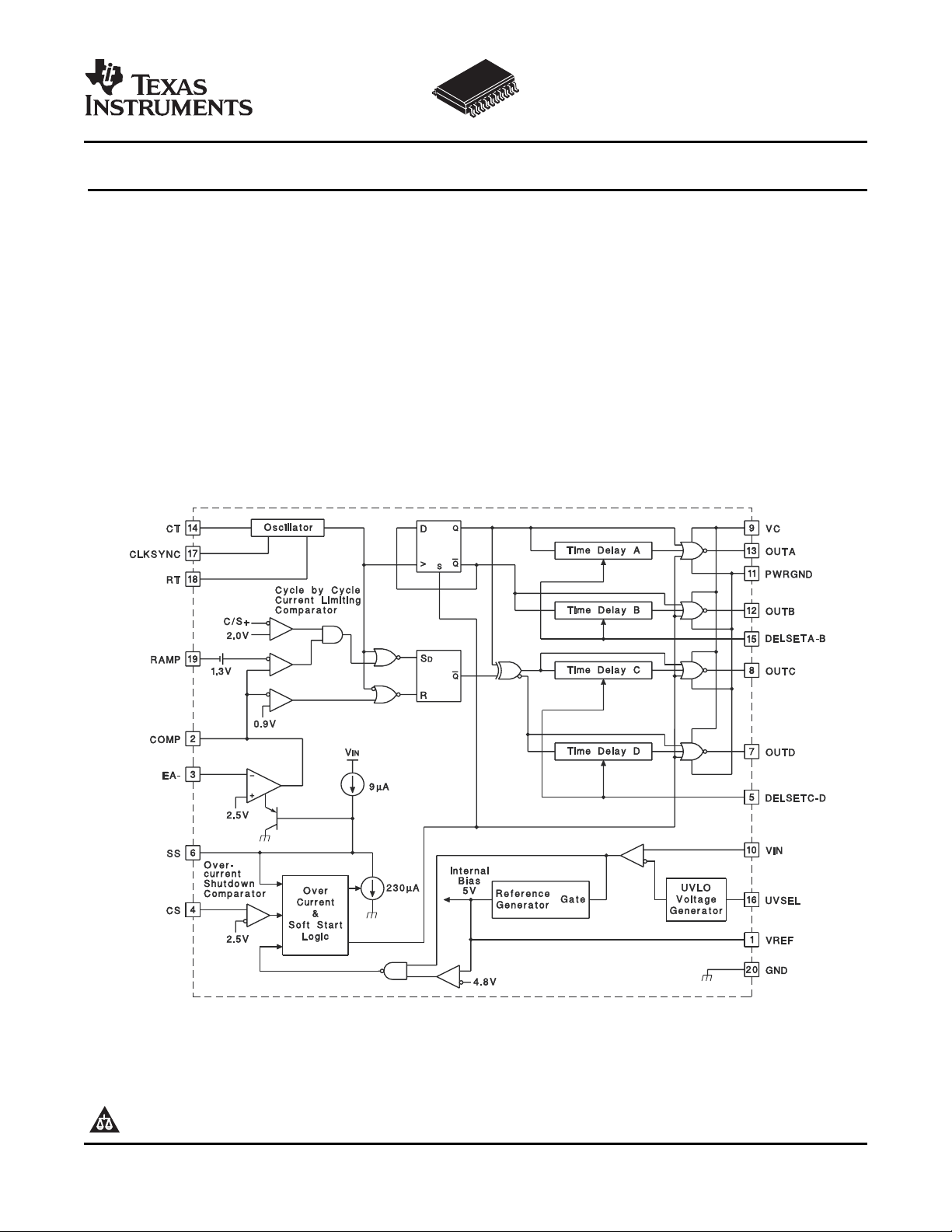
BLOCK DIAGRAM
UC1879
UC2879
UC3879
SLUS230B – JUNE 1998 – REVISED JUNE 2007
The UC3879 controls a bridge power stage by phase
shifting the switching of one half-bridge with respect
to the other. This allows constant frequency pulse
width modulation in combination with resonant,
zero-voltage switching for high efficiency
performance. The UC3879 can be configured to
provide control in either voltage mode or current
mode operation, with overcurrent shutdown for fast
fault protection.
Independently programmable time delays provide
dead-time at the turn-on of each output stage,
allowing time for each resonant switching interval.
Please be aware that an important notice concerning availability, standard warranty, and use in critical applications of Texas
Instruments semiconductor products and disclaimers thereto appears at the end of this data sheet.
PRODUCTION DATA information is current as of publication date.
Products conform to specifications per the terms of the Texas
Instruments standard warranty. Production processing does not
necessarily include testing of all parameters.
Copyright © 1998–2007, Texas Instruments Incorporated
Page 2
www.ti.com
UC1879
UC2879
UC3879
SLUS230B – JUNE 1998 – REVISED JUNE 2007
DESCRIPTION (CONTINUED)
With the oscillator capable of operating in excess of 600 kHz, overall output switching frequencies to 300 kHz
are practical. In addition to the standard free running mode, with the CLKSYNC pin, the user may configure the
UC3879 to accept an external clock synchronization signal. Alternatively, up to three units can be locked
together with the operational frequency determined by the fastest device.
Protective features include an undervoltage lockout and overcurrent protection. Additional features include a
10-MHz error amplifier, a 5-V precision reference, and soft start. The UC3879 is available in 20 pin N, J, DW,
and Q and 28 pin L packages.
ABSOLUTE MAXIMUM RATINGS
PARAMETER VALUE UNIT
Supply voltage (VC, VIN) 20 V
Output current, source or sink, dc 20
Output current, source, sink peak for 0.1 µ s at max frequency of 300
kHz
Analog inputs
(Pins 1, 2, 3, 4, 5, 6, 14, 15, 17, 18, 19) –0.3 to 5.3
(Pin 16) –0.03 to VIN
Analog outputs
(Pins 7, 8, 12, 13) –0.3 to VCto 0.3 V
Storage temperature range –65 ° C to 150 ° C
Junction temperature –55 ° C to 150 ° C ° C
Lead temperature (soldering, 10 sec) 300°C
(1) Pin references are to 20-pin DIL and SOIC packages. All voltages are with respect to ground unless otherwise stated. Currents are
positive into, negative out of the specified terminal.
(1)
100
THERMAL CHARACTERISTICS
over operating free-air temperature range (unless otherwise noted)
PACKAGE θ
J-20 70-85 28
N-20 80
DW-20 SOIC 45-95
PLCC-20 43-75
CLCC-20 N/A 5-8
(1) θJCdata values stated were derived from MIL-STD-1835B. MIL-STD-1835B states "The baseline values shown are worst case (mean
+2s) for a 60 x 60 mil microcircuit device silicon die and aplicable for devices with die sizes up to 14400 square mils. For devices die
sizes greater than 14400 square mils use the following values; dual-in-line, 11 ° C/W; flat pacl 10 ° C/W; pin grid array, 10 ° C/W".
(2) Specified θJA(junction-to-ambient) is for devices mounted to 5-in
resistance range is given, lower values are for 5-in
trace widths for power packages and 1.3-mm trace widths for non-power packages with a 100 x 100 mil probe land area at the end of
each trace.
(3) θJCestimated for backside of device, through the metalized thermal conduction pads.
2
aluminum PC board. Test PWB was 0.062 in thick and typically used 0.635-mm
JA
(2)
(2)
(2)
2
FR4 PC board with one ounce copper wire where noted. When
θ
JC
(1)
35
25
34
(2) (3)
mA
V
2
Submit Documentation Feedback
Page 3
www.ti.com
RT
RAMP
GND
CLKSYNC
UVSEL
CT
DELSETA-B
OUTA
1
2
3
4
5
6
7
8
20
19
18
17
16
15
14
13
COMP
VREF
OUTC
SS
OUTD
EA–
CS
DELSETC-D
9
10VIN
VC
OUTB
PWRGND
12
11
DIL-20,SOIC-2
JORNPACKAGE,DWPACKAGE
(TOP VIEW)
N/C
N/C
DELSETA-B
CT UVSEL
CLKSYNC
N/C
RT
RAMP
GND
N/C
N/C
VREF
COMP
1
4
3
2
28
27
25
242322 21
20
18
17
16
15
14
13
6
7
111098
EA–
CS
N/C
DELSETC-D
SS
N/C
N/C
OUTD
OUTC
VC
VIN
PWRGND
OUTB
OUTC
CLCC-28
(TOP VIEW)
L PACKAGE
3
18
17
16
DELSETC-D
12
20
19
15
14
4
5
6
7
8
9
13
10
11 12
SS
OUTD
CS
EA–
COMP
VREF
GND
RAMP
RT
OUTC
VC
VIN
PWRGND
OUTB
CLKSYNC
UVSEL
DELSETA-B
OUTA
CT
PLCC-20
QPACKAGE
(TOP VIEW)
SLUS230B – JUNE 1998 – REVISED JUNE 2007
Product Selection Guide
TEMPERATURE RANGE AVAILABLE PACKAGES
UCC1879 –55 ° C to 125 ° C J, L
UCC2879 –40 ° C to 85 ° C N, DW, Q, J, L
UCC3879 0 ° C to 70 ° C N, DW, Q
UC1879
UC2879
UC3879
Submit Documentation Feedback
3
Page 4
www.ti.com
UC1879
UC2879
UC3879
SLUS230B – JUNE 1998 – REVISED JUNE 2007
ELECTRICAL CHARACTERISTICS
Unless specified; VC = VIN = V
= 0.01 µ F, TA= TJ.
PARAMETER TEST CONDITIONS MIN TYP MAX UNIT
Undervoltage Lockout
Start threshold
UVLO hysteresis
Input bias, UVSEL pin V
Supply Current
I
startup 150 600
VIN
IVCstartup 10 100
I
operating
VIN
IVCoperating 4 8
Voltage Reference
Output voltage TJ= 25 ° C 4.92 5 5.08 V
Line regulation 11 V < VIN < 18 V 1 10
Load regulation I
Total variation Line, Load, Temperature 4.875 5.125 V
Short circuit current VREF = 0 V, TJ= 25 ° C –60 –15 mA
Error Amplifier
Error amplifier input voltage 2.4 2.5 2.6 V
Input bias current 0.6 3 µ A
AVOL 1 V < VCOMP < 4 V 60 90
PSRR 11 V < VIN < 18 V 85 100
Output sink current V
Output source current V
Output voltage high I
Output voltage low I
Slew rate TA= 25 ° C 6 11 V/ µ s
= 12 V, CT = 470 pF, RT = 9.53k, R
UVSEL
V
= VIN 9 10.75 12.5
UVSEL
V
= Open 12.5 15.25 16.5
UVSEL
V
= VIN 1.15 1.75 2.15
UVSEL
V
= Open 5.2 6 7.4
UVSEL
= VIN = 8 V 30 µ A
UVSEL
VIN = V
I
DELSETA-B
VIN = V
I
DELSETA-B
UVSEL
= I
UVSEL
= I
= 8 V, VC = 18 V,
DELSETC-D = 0
= 8 V, VC = 18 V,
DELSETC-D = 0
UC3879, UC2879 23 35
UC1879 23 36 mA
= –10 mA 5 20
VREF
= 1 V 1 2.5
COMP
= 4 V –1.3 –0.5
COMP
= –0.5 mA 4 4.7 5
COMP
= 1 mA 0 0.5 1
COMP
DELSETA-B
= R
DELSEC-D
= 4.8k, C
DELSETA-B
= C
DELSETC-D
V
µ A
mV
dB
mA
V
4
Submit Documentation Feedback
Page 5
www.ti.com
200
%
T
q = f
SLUS230B – JUNE 1998 – REVISED JUNE 2007
ELECTRICAL CHARACTERISTICS (continued)
Unless specified; VC = VIN = V
= 0.01 µ F, TA= TJ.
PARAMETER TEST CONDITIONS MIN TYP MAX UNIT
PWM Comparator
RAMP offset voltage TJ= 25 ° C
PWM phase shift,
T
DELSETA-B
, T
DELSETC-D
Output skew,
T
DELSETA-B
, T
DELSETC-D
Ramp to output delay,
T
DELSETA-B
= 0, T
DELSETC-D
Oscillator
Initial accuracy TA= 25 ° C 180 200 220 kHz
Voltage stability 11 V < VIN < 18 V 1 2 %
Total variation Line, Temperature 160 200 240 kHz
CLKSYNC threshold 2.3 2.5 2.7
Clock out high 2.8 4 V
Clock out low 0.5 1 1.5
Clock out pulse width 400 600 ns
Ramp valley voltage 0.2 0.4
Ramp peak voltage 2.8 2.9 3.2
Current Limit
Input bias V
Threshold voltage 2.35 2.5 2.65 V
Delay to OUTA, B, C, D 160 300 ns
Cycle-by-Cycle Current Limit
Input bias V
Threshold voltage 1.85 2 2.15 V
Delay to output zero phase 110 300 ns
(1) Ramp offset voltage has a temperature coefficient of about –4 mV/ ° C.
(2)
= 0
(2)
= 0
= 0
= 12 V, CT = 470 pF, RT = 9.53k, R
UVSEL
(1)
V
> V
COMP
V
COMP
V
COMP
V
COMP
RAMPpeak
< Zero Phase Shift Voltage 0% 0.3% 2%
> V
RAMPpeak
< Zero Phase Shift Voltage 10
UC3879, UC2879 115 250
UC1879 115 300
= 3 V 2 10 µ A
CS
= 2.2 V 2 10 µ A
CS
DELSETA-B
= R
DELSEC-D
= 4.8k, C
DELSETA-B
1.1 1.25 1.4 V
+ V
RAMPoffset
+ V
RAMPoffset
98% 99.7% 102%
10
UC1879
UC2879
UC3879
= C
DELSETC-D
ns
V
(2) Phase shift percentage (0% = 0 , 100% = 180 ) is defined as
where is the phase shift, and and T are defined in Figure 1 . At 0% phase shift, is the output skew.
Submit Documentation Feedback
5
Page 6

www.ti.com
(
)
10
DELAY
Delay Time 0.89 10 R sec
-
= · ·
1
delay T duty cycle
2
æ ö
= · -
ç ÷
è ø
t
DutyCycleT=
Period T=
DHL DHL
T (A toC) T (Bto D)= =
UC1879
UC2879
UC3879
SLUS230B – JUNE 1998 – REVISED JUNE 2007
ELECTRICAL CHARACTERISTICS (continued)
Unless specified; VC = VIN = V
= 0.01 µ F, TA= TJ.
PARAMETER TEST CONDITIONS MIN TYP MAX UNIT
Soft Start/Reset Delay
Charge current V
Discharge current V
Restart threshold 4.3 4.7 V
Discharge level 300 mV
Output Drivers
Output Low level I
Output High level I
Delay Set
(3) Delay time can be programmed via resistors from the delay set pins to ground.
(3)
Delay time
Delay time
Zero delay
(4)
(4)
(5)
= 12 V, CT = 470 pF, RT = 9.53k, R
UVSEL
= 0.5 V –20 –9 –3
SS
= 1 V 120 230
SS
= 10 mA 0.3 0.4
OUT
= –10 mA, Referenced to VC 2.2 3
OUT
R
DELSETA-B
R
DELSETA-B
V
DELSETA-B
= R
= R
= V
DELSETA-B
DELSETC-D
DELSETC-D
DELSETC-D
= 4.8k 250 370 520
= 1.9k 100 155 220 ns
= 5 V 5
= R
DELSEC-D
= 4.8k, C
DELSETA-B
= C
DELSETC-D
µ A
V
The recommended range for R
(4) Delay time is defined as:
where T is defined in Figure 1 .
(5) The zero phase shift voltage is the voltage measured at COMP which forces zero phase shift. This condition corresponds to zero
effective output power. Zero phase shift voltage has a temperature coefficient of about –2 mV/ ° C.
is 1.9 k Ω to 10 k Ω .
DELAY
Figure 1. Phase Shift, Output Skew and Delay Time Definitions
6
Submit Documentation Feedback
Page 7

www.ti.com
Dlin
CT
1.08 RT=· · f
UC1879
UC2879
UC3879
SLUS230B – JUNE 1998 – REVISED JUNE 2007
PIN DESCRIPTIONS
CLKSYNC (Bi-directional Clock and Synchronization): Used as an output, CLKSYNC provides a clock signal. As
an input, this pin provides a synchronization point. Multiple UC3879s, each with their own local oscillator
frequency, may be connected together by the CLKSYNC pin, and they will synchronize to the fastest oscillator.
This pin may also be used to synchronize the UC3879 to an external clock, provided the frequency of the
external signal is higher than the frequency of the local oscillator. CLKSYNC is internally connected to an emitter
follower pull-up and a current source pull-down (300 µ A typical). Therefore, an external resistor to GND can be
used to improve the CLKSYNC pin’s ability to drive capacitive loads.
COMP (Error Amplifier Output): This pin is the output of the gain stage for overall feedback control. Error
amplifier output voltage levels below 0.9 V forces zero phase shift. Since the error amplifier has a relatively low
current drive capability, the output may be overridden by driving it with a sufficiently low impedance source.
CT (Oscillator Frequency Set): After choosing RT to set the required upper end of the linear duty cycle range,
the timing capacitor (CT) value is calculated to set the oscillator frequency as follows:
Connect the timing capacitor directly between CT and GND. Use a high quality ceramic capacitor with low ESL
and ESR for best results. A minimum CT value of 200 pF insures good accuracy and less susceptibility to circuit
layout parasitics. The oscillator and PWM are designed to provide practical operation to 600 kHz.
CS (Current Sense): This pin is the non-inverting input to the two current fault comparators whose references
are set internally to fixed values of 2 V and 2.5 V. When the voltage at this pin exceeds 2 V, and the error
amplifier output voltage exceeds the voltage on the ramp input, the phase shift limiting overcurrent comparator
will limit the phase shifting on a cycle-by-cycle basis. When the voltage at this pin exceeds 2.5 V, the current
fault latch is set, the outputs are forced OFF, and a soft start cycle is initiated. If a constant voltage above 2.5 V
is applied to this pin the outputs are disabled and held low. When CS is brought below 2.5 V, the outputs will
begin switching at 0 degrees phase shift before the SS pin begins to rise. This condition will not prematurely
deliver power to the load.
DELSETA-B, DELSETC-D (Output Delay Control): The user programmed currents from these pins to GND set
the turn on delay for the corresponding output pair. This delay is introduced between the turn off of one switch
and the turn on of another in the same leg of the bridge to allow resonant switching to take place. Separate
delays are provided for the two half-bridges to accommodate differences in the resonant capacitor charging
currents.
EA– (Error Amplifier Inverting Input): This is normally connected to the voltage divider resistors which sense the
power supply output voltage level. The loop compensation components are connected between this pin and
COMP.
GND (Signal Ground): All voltages are measured with respect to GND. The timing capacitor on CT, and bypass
capacitors on VREF and VIN should be connected directly to the ground plane near GND.
OUTA – OUTD (Outputs A-D): The outputs are 100-mA totem pole output drivers optimized to drive FET driver
devices. The outputs operate as pairs with a nominal 50% duty cycle. The A-B pair is intended to drive one
half-bridge in the external power stage and is synchronized to the clock waveform. The C-D pair drives the other
half-bridge with switching phase shifted with respect to the A-B outputs.
PWRGND (Power Ground): VC should be bypassed with a ceramic capacitor from VC to the section of the
ground plane that is connected to PWRGND. Any required bulk reservoir capacitor should be connected in
parallel. PWRGND and GND should be connected at a single point near the chip to optimize noise rejection and
minimize DC voltage drops.
RAMP (Voltage Ramp): This pin is the input to the PWM comparator. Connect it to CT for voltage mode control.
For current mode control, connect RAMP to CS and also to the output of the current sense transformer circuit.
Slope compensation can be achieved by injecting a portion of the ramp voltage from CT to RAMP.
Submit Documentation Feedback
7
Page 8

www.ti.com
( )
2.5
RT
10 mA 1 Dlin
=
· -
UC1879
UC2879
UC3879
SLUS230B – JUNE 1998 – REVISED JUNE 2007
PIN DESCRIPTIONS (continued)
RT (Clock/Sync Duty Cycle Set Pin): The UC3879 oscillator produces a sawtooth waveform. The rising edge is
generated by connecting a resistor from RT to GND and a capacitor from CT to GND (see CT pin description).
During the rising edge, the modulator has linear control of the duty cycle. The duty cycle jumps to 100% when
the voltage on COMP exceeds the oscillator peak voltage. Selection of RT should be done first, based on the
required upper end of the linear duty cycle range (D
Recommended values for RT range from 2.5 k Ω to 100 k Ω .
SS: Connect a capacitor between this pin and GND to set the soft start time. The voltage at SS will remain near
zero volts as long as VIN is below the UVLO threshold. Soft start will be pulled up to about 4.8 V by an internal
9- µ A current source when VIN and VREF become valid (assuming a non-fault condition). In the event of a
current fault (CS voltage exceeding 2.5 V), soft start will be pulled to GND and then ramp to 4.8 V. If a fault
occurs during the soft start cycle, the outputs will be immediately disabled and soft start must fully charge prior
to resetting the fault latch. For paralleled controllers, the soft start pins may be paralleled to a single capacitor,
but the charge currents will be additive.
UVSEL: Connecting this pin to VIN sets a turn on voltage of 10.75 V with 1.5 V of UVLO hysteresis. Leaving the
pin open-circuited programs a turn on voltage of 15.25 V with 6 V of hysteresis.
VC (Output Switch Supply Voltage): This pin supplies power to the output drivers and their associated bias
circuitry. The difference between the output high drive and VC is typically 2.1 V. This supply should be bypassed
directly to PWRGND with a low ESR/ESL capacitor.
VIN (Primary Chip Supply Voltage): This pin supplies power to the logic and analog circuitry on the integrated
circuit that is not directly associated with driving the output stages. Connect VIN to a stable source above 12 V
for normal operation. To ensure proper functionality, the UC3879 is inactive until VIN exceeds the upper
undervoltage lockout threshold. This pin should be bypassed directly to GND with a low ESR/ESL capacitor.
) as follows:
lin
NOTE:
When VIN exceeds the UVLO threshold the supply current (IIN) jumps from about 100
A to greater than 20 mA. If the UC3879 is not connected to a well bypassed supply, it
may immediately enter the UVLO state again. Therefore, sufficient bypass capacity
must be added to ensure reliable startup.
VREF: This pin provides an accurate 5 V voltage reference. It is internally short circuit current limited. VREF is
disabled while VIN is below the UVLO threshold. The circuit is also disabled until VREF reaches approximately
4.75 V. For best results bypass VREF with a 0.1 µ F, low ESR/ESL capacitor.
ADDITIONAL INFORMATION
Please refer to the following Unitrode publications for additional information. The following three topics are
available in the Applications Handbook.
1. Application Note U-154, The New UC3879 Phase- Shifted PWM Controller Simplifies the Design of Zero
Voltage Transition Full-Bridge Converters, by Laszlo Balogh.
2. Application Note U-136, Phase Shifted, Zero Voltage Transition Design Considerations and the UC3875
PWM Controller, by Bill Andreycak.
3. Design Note DN-63, The Current-Doubler Rectifier: An Alternative Rectification Technique for Push-Pull
and Bridge Converters, by Laszlo Balogh.
8
Submit Documentation Feedback
Page 9

PACKAGE OPTION ADDENDUM
www.ti.com
17-Dec-2007
PACKAGING INFORMATION
Orderable Device Status
(1)
Package
Type
Package
Drawing
Pins Package
Qty
Eco Plan
UC1879J OBSOLETE CDIP J 20 TBD Call TI Call TI
UC1879J883B OBSOLETE CDIP J 20 TBD Call TI CallTI
UC2879DW ACTIVE SOIC DW 20 25 Green (RoHS &
no Sb/Br)
UC2879DWG4 ACTIVE SOIC DW 20 25 Green (RoHS &
no Sb/Br)
UC2879DWTR ACTIVE SOIC DW 20 2000 Green (RoHS &
no Sb/Br)
UC2879DWTRG4 ACTIVE SOIC DW 20 2000 Green (RoHS &
no Sb/Br)
UC2879J OBSOLETE CDIP J 20 TBD Call TI Call TI
UC2879N ACTIVE PDIP N 20 20 Green (RoHS &
no Sb/Br)
UC2879NG4 ACTIVE PDIP N 20 20 Green (RoHS &
no Sb/Br)
UC3879DW ACTIVE SOIC DW 20 25 Green (RoHS &
no Sb/Br)
UC3879DWG4 ACTIVE SOIC DW 20 25 Green (RoHS &
no Sb/Br)
UC3879DWTR ACTIVE SOIC DW 20 2000 Green (RoHS &
no Sb/Br)
UC3879DWTRG4 ACTIVE SOIC DW 20 2000 Green (RoHS &
no Sb/Br)
UC3879J OBSOLETE CDIP J 20 TBD Call TI Call TI
UC3879N ACTIVE PDIP N 20 20 Green (RoHS &
no Sb/Br)
UC3879NG4 ACTIVE PDIP N 20 20 Green (RoHS &
no Sb/Br)
(1)
The marketing status values are defined as follows:
ACTIVE: Product device recommended for new designs.
LIFEBUY: TI has announced that the device will be discontinued, and a lifetime-buy period is in effect.
NRND: Not recommended for new designs. Device is in production to support existing customers, but TI does not recommend using this part in
a new design.
PREVIEW: Device has been announced but is not in production. Samples may or may not be available.
OBSOLETE: TI has discontinued the production of the device.
(2)
Lead/Ball Finish MSL Peak Temp
CU NIPDAU Level-2-260C-1 YEAR
CU NIPDAU Level-2-260C-1 YEAR
CU NIPDAU Level-2-260C-1 YEAR
CU NIPDAU Level-2-260C-1 YEAR
Call TI N / A for Pkg Type
Call TI N / A for Pkg Type
CU NIPDAU Level-2-260C-1 YEAR
CU NIPDAU Level-2-260C-1 YEAR
CU NIPDAU Level-2-260C-1 YEAR
CU NIPDAU Level-2-260C-1 YEAR
Call TI N / A for Pkg Type
Call TI N / A for Pkg Type
(3)
(2)
Eco Plan - The planned eco-friendly classification: Pb-Free (RoHS), Pb-Free (RoHS Exempt), or Green (RoHS & no Sb/Br) - please check
http://www.ti.com/productcontent for the latest availability information and additional product content details.
TBD: The Pb-Free/Green conversion plan has not been defined.
Pb-Free (RoHS): TI's terms "Lead-Free" or "Pb-Free" mean semiconductor products that are compatible with the current RoHS requirements
for all 6 substances, including the requirement that lead not exceed 0.1% by weight in homogeneous materials. Where designed to be soldered
at high temperatures, TI Pb-Free products are suitable for use in specified lead-free processes.
Pb-Free (RoHS Exempt): This component has a RoHS exemption for either 1) lead-based flip-chip solder bumps used between the die and
package, or 2) lead-based die adhesive used between the die and leadframe. The component is otherwise considered Pb-Free (RoHS
compatible) as defined above.
Green (RoHS & no Sb/Br): TI defines "Green" to mean Pb-Free (RoHS compatible), and free of Bromine (Br) and Antimony (Sb) based flame
retardants (Br or Sb do not exceed 0.1% by weight in homogeneous material)
(3)
MSL, Peak Temp. -- The Moisture Sensitivity Level rating according to the JEDEC industry standard classifications, and peak solder
temperature.
Addendum-Page 1
Page 10

PACKAGE OPTION ADDENDUM
www.ti.com
Important Information and Disclaimer:The information provided on this page represents TI's knowledge and belief as of the date that it is
provided. TI bases its knowledge and belief on information provided by third parties, and makes no representation or warranty as to the
accuracy of such information. Efforts are underway to better integrate information from third parties. TI has taken and continues to take
reasonable steps to provide representative and accurate information but may not have conducted destructive testing or chemical analysis on
incoming materials and chemicals. TI and TI suppliers consider certain information to be proprietary, and thus CAS numbers and other limited
information may not be available for release.
In no event shall TI's liability arising out of such information exceed the total purchase price of the TI part(s) at issue in this document sold by TI
to Customer on an annual basis.
17-Dec-2007
Addendum-Page 2
Page 11

PACKAGE MATERIALS INFORMATION
www.ti.com
TAPE AND REEL INFORMATION
11-Mar-2008
*All dimensions are nominal
Device Package
UC2879DWTR SOIC DW 20 2000 330.0 24.4 10.8 13.0 2.7 12.0 24.0 Q1
UC3879DWTR SOIC DW 20 2000 330.0 24.4 10.8 13.0 2.7 12.0 24.0 Q1
Type
Package
Drawing
Pins SPQ Reel
Diameter
(mm)
Reel
Width
W1 (mm)
A0 (mm) B0 (mm) K0 (mm) P1
(mm)W(mm)
Pin1
Quadrant
Pack Materials-Page 1
Page 12

PACKAGE MATERIALS INFORMATION
www.ti.com
11-Mar-2008
*All dimensions are nominal
Device Package Type Package Drawing Pins SPQ Length (mm) Width (mm) Height (mm)
UC2879DWTR SOIC DW 20 2000 346.0 346.0 41.0
UC3879DWTR SOIC DW 20 2000 346.0 346.0 41.0
Pack Materials-Page 2
Page 13

Page 14

Page 15

Page 16

IMPORTANT NOTICE
Texas Instruments Incorporated and its subsidiaries (TI) reserve the right to make corrections, modifications, enhancements, improvements,
and other changes to its products and services at any time and to discontinue any product or service without notice. Customers should
obtain the latest relevant information before placing orders and should verify that such information is current and complete. All products are
sold subject to TI’s terms and conditions of sale supplied at the time of order acknowledgment.
TI warrants performance of its hardware products to the specifications applicable at the time of sale in accordance with TI’s standard
warranty. Testing and other quality control techniques are used to the extent TI deems necessary to support this warranty. Except where
mandated by government requirements, testing of all parameters of each product is not necessarily performed.
TI assumes no liability for applications assistance or customer product design. Customers are responsible for their products and
applications using TI components. To minimize the risks associated with customer products and applications, customers should provide
adequate design and operating safeguards.
TI does not warrant or represent that any license, either express or implied, is granted under any TI patent right, copyright, mask work right,
or other TI intellectual property right relating to any combination, machine, or process in which TI products or services are used. Information
published by TI regarding third-party products or services does not constitute a license from TI to use such products or services or a
warranty or endorsement thereof. Use of such information may require a license from a third party under the patents or other intellectual
property of the third party, or a license from TI under the patents or other intellectual property of TI.
Reproduction of TI information in TI data books or data sheets is permissible only if reproduction is without alteration and is accompanied
by all associated warranties, conditions, limitations, and notices. Reproduction of this information with alteration is an unfair and deceptive
business practice. TI is not responsible or liable for such altered documentation. Information of third parties may be subject to additional
restrictions.
Resale of TI products or services with statements different from or beyond the parameters stated by TI for that product or service voids all
express and any implied warranties for the associated TI product or service and is an unfair and deceptive business practice. TI is not
responsible or liable for any such statements.
TI products are not authorized for use in safety-critical applications (such as life support) where a failure of the TI product would reasonably
be expected to cause severe personal injury or death, unless officers of the parties have executed an agreement specifically governing
such use. Buyers represent that they have all necessary expertise in the safety and regulatory ramifications of their applications, and
acknowledge and agree that they are solely responsible for all legal, regulatory and safety-related requirements concerning their products
and any use of TI products in such safety-critical applications, notwithstanding any applications-related information or support that may be
provided by TI. Further, Buyers must fully indemnify TI and its representatives against any damages arising out of the use of TI products in
such safety-critical applications.
TI products are neither designed nor intended for use in military/aerospace applications or environments unless the TI products are
specifically designated by TI as military-grade or "enhanced plastic." Only products designated by TI as military-grade meet military
specifications. Buyers acknowledge and agree that any such use of TI products which TI has not designated as military-grade is solely at
the Buyer's risk, and that they are solely responsible for compliance with all legal and regulatory requirements in connection with such use.
TI products are neither designed nor intended for use in automotive applications or environments unless the specific TI products are
designated by TI as compliant with ISO/TS 16949 requirements. Buyers acknowledge and agree that, if they use any non-designated
products in automotive applications, TI will not be responsible for any failure to meet such requirements.
Following are URLs where you can obtain information on other Texas Instruments products and application solutions:
Products Applications
Amplifiers amplifier.ti.com Audio www.ti.com/audio
Data Converters dataconverter.ti.com Automotive www.ti.com/automotive
DSP dsp.ti.com Broadband www.ti.com/broadband
Clocks and Timers www.ti.com/clocks Digital Control www.ti.com/digitalcontrol
Interface interface.ti.com Medical www.ti.com/medical
Logic logic.ti.com Military www.ti.com/military
Power Mgmt power.ti.com Optical Networking www.ti.com/opticalnetwork
Microcontrollers microcontroller.ti.com Security www.ti.com/security
RFID www.ti-rfid.com Telephony www.ti.com/telephony
RF/IF and ZigBee® Solutions www.ti.com/lprf Video & Imaging www.ti.com/video
Mailing Address: Texas Instruments, Post Office Box 655303, Dallas, Texas 75265
Copyright © 2008, Texas Instruments Incorporated
Wireless www.ti.com/wireless
 Loading...