

VO(nom)
0°C to 125°C
www.DataSheet4U.com
µA7900 SERIES
NEGATIVE-VOLTAGE REGULATORS
SLVS058A – JUNE 1976 – REVISED OCTOBER 1996
D
3-Terminal Regulators
D
Output Current Up to 1.5 A
D
No External Components
D
Internal Thermal Overload Protection
D
High-Power Dissipation Capability
D
Internal Short-Circuit Current Limiting
D
Output Transistor Safe-Area Compensation
D
Essentially Equivalent to National LM320
Series
description
This series of fixed-negative-voltage monolithic
integrated-circuit voltage regulators is designed
to complement Series µA7800 in a wide range of
applications. These applications include on-card
regulation for elimination of noise and distribution
problems associated with single-point regulation.
Each of these regulators can deliver up to 1.5 A of
output current. The internal current limiting and
thermal shutdown features of these regulators
make them essentially immune to overload. In
addition to use as fixed-voltage regulators, these
devices can be used with external components to
obtain adjustable output voltages and currents
and also as the power pass element in precision
regulators.
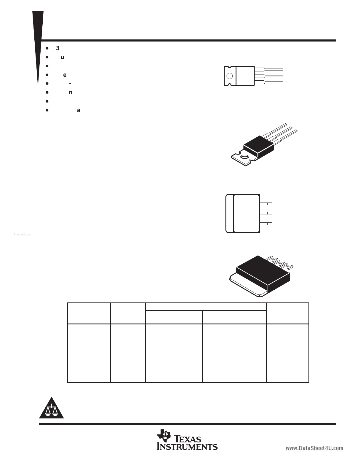
KC PACKAGE
(TOP VIEW)
OUTPUT
INPUT
COMMON
The input terminal is in electrical
contact with the mounting base
TO–220AB
O
I
KTE PACKAGE
(TOP VIEW)
OUTPUT
INPUT
COMMON
The input terminal is in electrical contact with the mounting base.
C
T
A
°
†
The KTE package is also available taped and reeled.
Please be aware that an important notice concerning availability, standard warranty, and use in critical applications of
Texas Instruments semiconductor products and disclaimers thereto appears at the end of this data sheet.
PRODUCTION DATA information is current as of publication date.
Products conform to specifications per the terms of Texas Instruments
standard warranty. Production processing does not necessarily include
testing of all parameters.
°
(V)
–5 µA7905CKC µA7905CKTE µA7905Y
–5.2 µA7952CKC µA7952CKTE µA7952Y
–6 µA7906CKC µA7906CKTE µA7906Y
–8 µA7908CKC µA7908CKTE µA7908Y
–12 µA7912CKC µA7912CKTE µA7912Y
–15 µA7915CKC µA7915CKTE µA7915Y
–18 µA7918CKC µA7918CKTE µA7918Y
–24 µA7924CKC µA7924CKTE µA7924Y
AVAILABLE OPTIONS
PACKAGED DEVICES
HEAT-SINK MOUNTED
(KC)
HEAT-SINK MOUNTED
(KTE)
Copyright 1996, Texas Instruments Incorporated
O
I
C
CHIP
†
FORM
(Y)
POST OFFICE BOX 655303 • DALLAS, TEXAS 75265
1
µA7900 SERIES
www.DataSheet4U.com
NEGATIVE-VOLTAGE REGULATORS
SLVS058A – JUNE 1976 – REVISED OCTOBER 1996
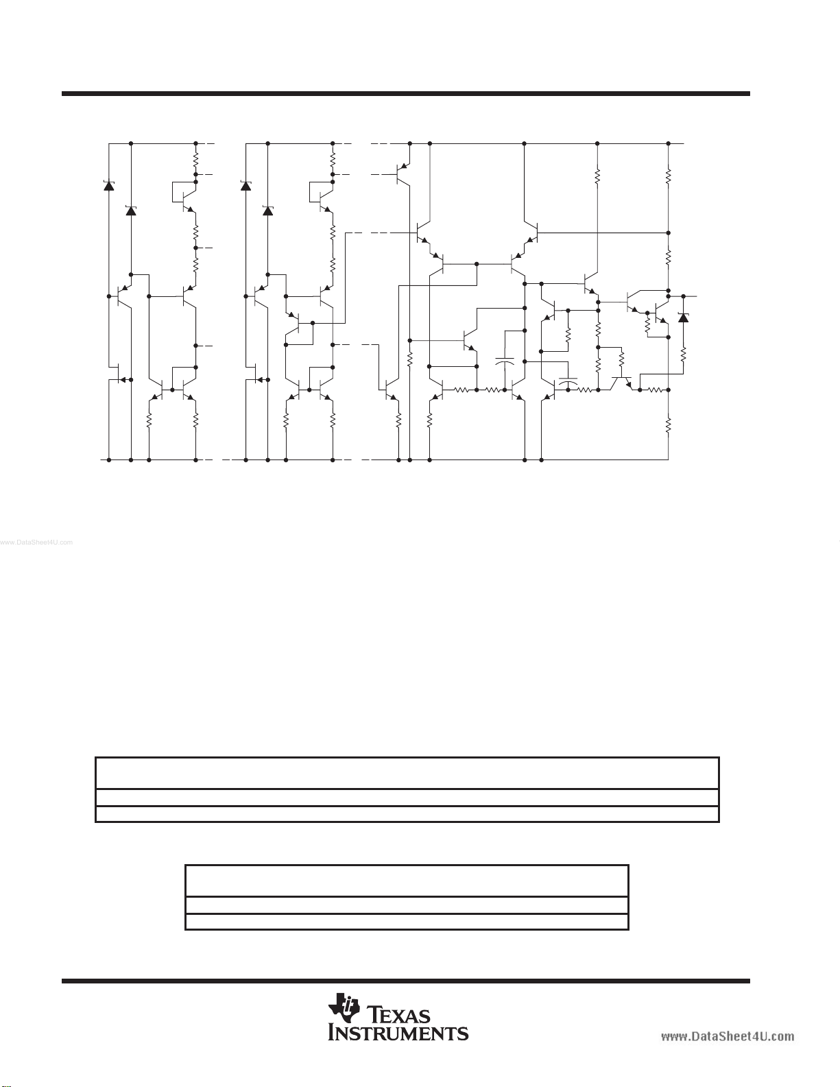
schematic
5 V to 8 V
12 V to 18 V
COMMON
5 kΩ
OUTPUT
6.2 V
20 kΩ
0.2 kΩ
INPUT
All component values are nominal.
INPUT
absolute maximum ratings over operating temperature range (unless otherwise noted)
Input voltage, VI: µA7924C –40 V. . . . . . . . . . . . . . . . . . . . . . . . . . . . . . . . . . . . . . . . . . . . . . . . . . . . . . . . . . . . . . . .
All others –35 V. . . . . . . . . . . . . . . . . . . . . . . . . . . . . . . . . . . . . . . . . . . . . . . . . . . . . . . . . . . . . . . .
Continuous total power dissipation at (or below):T
Operating free-air, T
Storage temperature range, T
, case, TC, or virtual junction, TJ, temperature range 0 to 150°C. . . . . . . . . . . . . . . . . . .
A
–65 to 150°C. . . . . . . . . . . . . . . . . . . . . . . . . . . . . . . . . . . . . . . . . . . . . . . . . . . . .
stg
Lead temperature 3.2 mm (1/8 inch) from case for 10 seconds 260°C. . . . . . . . . . . . . . . . . . . . . . . . . . . . . . . . .
NOTE 1: For operation above 25°C free-air or 90°C case temperature, refer to Figures 1 and 2. T o avoid exceeding the design maximum virtual
junction temperature, these ratings should not be exceeded. Due to variations in individual device electrical characteristics and thermal
resistance, the built-in thermal overload protection may be activated at power levels slightly above or below the rated dissipation.
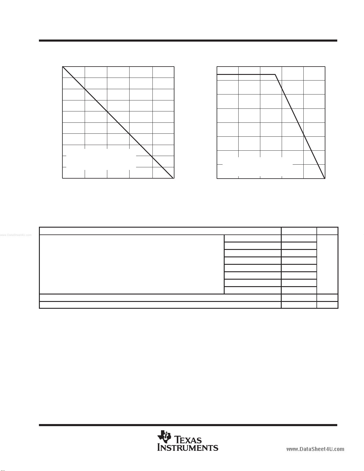
DISSIPATION RATING TABLE — FREE-AIR TEMPERATURE
PACKAGE
KC 2000 mW 16.0 mW/°C 1280 mW 720 mW 400 mW
KTE 1900 mW 15.2 mW/°C 1216 mW 684 mW 380 mW
TA ≤ 25°C
POWER RATING
DERATING FACTOR
ABOVE TA = 25°C
DISSIPATION RATING TABLE — CASE TEMPERATURE
= 25°C (see Note 1) See Dissipation Rating Tables. . .
A
T
= 90°C (see Note 1) See Dissipation Rating Tables. . .
C
TA = 70°C
POWER RATING
POWER RATING
TA = 105°C
TA = 125°C
POWER RATING
2
PACKAGE
KC 15000 mW 250.0 mW/°C 6250 mW
KTE 14300 mW 238.0 mW/°C 5970 mW
TC ≤ 90°C
POWER RATING
POST OFFICE BOX 655303 • DALLAS, TEXAS 75265
DERATING FACTOR
ABOVE TC = 90°C
TA = 125°C
POWER RATING
Input voltage, V
V
www.DataSheet4U.com
µA7900 SERIES
NEGATIVE-VOLTAGE REGULATORS
SLVS058A – JUNE 1976 – REVISED OCTOBER 1996
FREE-AIR TEMPERATURE
DISSIPATATION DERATING CURVE
2000
1800
1600
1400
1200
1000
800
600
400
200
Maximum Continuous Dissipation – mW
Derating factor = 16 mW/°C
R
≈ 62.5°C/W
θJA
0
25
50 75 100 125 150
TA – Free-Air Temperature – ° C
Figure 1 Figure 2
recommended operating conditions
p
Output current, I
Operating virtual junction temperature, T
I
O
J
CASE TEMPERATURE
DISSIPATION DERATING CURVE
16
14
12
10
8
6
4
Maximum Continuous Dissipation – W
Derating factor = 0.25 W/°C
2
above 90°C
R
≈ 4°C/W
θJA
0
25 50 75 100
TC – Case Temperature – °C
µA7905C –7 –25
µA7952C –7.2 –25
µA7906C –8 –25
µA7908C –10.5 –25
µA7912C –14.5 –30
µA7915C –17.5 –30
µA7918C –21 –33
µA7924C –27 –28
125 150
MIN MAX UNIT
1.5 A
0 125 °C
POST OFFICE BOX 655303 • DALLAS, TEXAS 75265
3

µA7900 SERIES
PARAMETER
TEST CONDITIONS
T
†
UNITS
‡
Input regulation
mV
Output regulation
mV
Bias current change
mA
PARAMETER
TEST CONDITIONS
T
†
UNITS
‡
Input regulation
mV
Output regulation
mV
Bias current change
mA
www.DataSheet4U.com
NEGATIVE-VOLTAGE REGULATORS
SLVS058A – JUNE 1976 – REVISED OCTOBER 1996
electrical characteristics at specified virtual junction temperature, VI = –10 V , IO = 500 mA (unless
otherwise noted)
J
25°C –4.8 –5 –5.2
Output voltage
p
Ripple rejection VI = –8 V to –18 V , f = 120 Hz 0°C to 125°C 54 60 dB
p
Temperature coefficient of output voltage IO = 5 mA 0°C to 125°C –0.4 mV/°C
Output noise voltage f = 10 Hz to 100 kHz 25°C 125 µV
Dropout voltage IO = 1 A 25°C 1.1 V
Bias current 25°C 1.5 2 mA
Peak output current 25°C 2.1 A
†
Pulse-testing techniques are used to maintain the junction temperature as close to the ambient temperature as possible. Thermal effects must
be taken into account separately. All characteristics are measured with a 2- µF capacitor across the input and a 1-µF capacitor across the output.
‡
This specification applies only for dc power dissipation permitted by absolute maximum ratings.
IO = 5 mA to 1 A,
P ≤ 15 W
VI = –7 V to –25 V 12.5 50
VI = –8 V to –12 V 4 15
IO = 5 mA to 1.5 A 15 100
IO = 250 mA to 750 mA 5 50
VI = –7 V to –25 V 0.15 0.5
IO = 5 mA to 1 A 0.08 0.5
VI = –7 V to –20 V , 0°C to 125°C –4.75 –5.25
µA7905C
MIN TYP MAX
V
electrical characteristics at specified virtual junction temperature, VI = –10 V , IO = 500 mA (unless
otherwise noted)
J
25°C –5 –5.2 –5.4
Output voltage
p
Ripple rejection VI = –8.2 V to –18 V , f = 120 Hz 0°C to 125°C 54 60 dB
p
Temperature coefficient of output voltage IO = 5 mA 0°C to 125°C –0.4 mV/°C
Output noise voltage f = 10 Hz to 100 kHz 25°C 125 µV
Dropout voltage IO = 1 A 25°C 1.1 V
Bias current 25°C 1.5 2 mA
Peak output current 25°C 2.1 A
†
Pulse-testing techniques are used to maintain the junction temperature as close to the ambient temperature as possible. Thermal effects must
be taken into account separately. All characteristics are measured with a 2- µF capacitor across the input and a 1-µF capacitor across the output.
‡
This specification applies only for dc power dissipation permitted by absolute maximum ratings.
IO = 5 mA to 1 A,
P ≤ 15 W
VI = –7.2 V to –25 V 12.5 100
VI = –8.2 V to –12 V 4 50
IO = 5 mA to 1.5 A 15 100
IO = 250 mA to 750 mA 5 50
VI = –7.2 V to –25 V 0.15 1.3
IO = 5 mA to 1 A 0.08 0.5
VI = –7.2 V to –20 V , 0°C to 125°C –4.95 –5.45
µA7952C
MIN TYP MAX
V
4
POST OFFICE BOX 655303 • DALLAS, TEXAS 75265

PARAMETER
TEST CONDITIONS
T
†
UNITS
‡
Input regulation
mV
Output regulation
mV
Bias current change
mA
PARAMETER
TEST CONDITIONS
T
†
UNITS
‡
Input regulation
mV
Output regulation
mV
Bias current change
mA
www.DataSheet4U.com
µA7900 SERIES
NEGATIVE-VOLTAGE REGULATORS
SLVS058A – JUNE 1976 – REVISED OCTOBER 1996
electrical characteristics at specified virtual junction temperature, VI = –11 V, IO = 500 mA (unless
otherwise noted)
J
25°C –5.75 –6 –6.25
Output voltage
p
Ripple rejection VI = –9 V to –19 V , f = 120 Hz 0°C to 125°C 54 60 dB
p
Temperature coefficient of output voltage IO = 5 mA 0°C to 125°C –0.4 mV/°C
Output noise voltage f = 10 Hz to 100 kHz 25°C 150 µV
Dropout voltage IO = 1 A 25°C 1.1 V
Bias current 25°C 1.5 2 mA
Peak output current 25°C 2.1 A
†
Pulse-testing techniques are used to maintain the junction temperature as close to the ambient temperature as possible. Thermal effects must
be taken into account separately. All characteristics are measured with a 2- µF capacitor across the input and a 1-µF capacitor across the output.
‡
This specification applies only for dc power dissipation permitted by absolute maximum ratings.
IO = 5 mA to 1 A,
P ≤ 15 W
VI = –8 V to –25 V 12.5 120
VI = –9 V to –13 V 4 60
IO = 5 mA to 1.5 A 15 120
IO = 250 mA to 750 mA 5 60
VI = –8 V to –25 V 0.15 1.3
IO = 5 mA to 1 A 0.08 0.5
VI = –8 V to –21 V ,
0°C to 125°C –5.7 –6.3
µA7906C
MIN TYP MAX
V
electrical characteristics at specified virtual junction temperature, VI = –14 V , IO = 500 mA (unless
otherwise noted)
J
25°C –7.7 –8 –8.3
Output voltage
p
Ripple rejection VI = –11.5 V to –21.5 V, f = 120 Hz 0°C to 125°C 54 60 dB
p
Temperature coefficient of output voltage IO = 5 mA 0°C to 125°C –0.6 mV/°C
Output noise voltage f = 10 Hz to 100 kHz 25°C 200 µV
Dropout voltage IO = 1 A 25°C 1.1 V
Bias current 25°C 1.5 2 mA
Peak output current 25°C 2.1 A
†
Pulse-testing techniques are used to maintain the junction temperature as close to the ambient temperature as possible. Thermal effects must
be taken into account separately. All characteristics are measured with a 2- µF capacitor across the input and a 1-µF capacitor across the output.
‡
This specification applies only for dc power dissipation permitted by absolute maximum ratings.
IO = 5 mA to 1 A,
P ≤ 15 W
VI = –10.5 V to –25 V 12.5 160
VI = –11 V to –17 V 4 80
IO = 5 mA to 1.5 A 15 160
IO = 250 mA to 750 mA 5 80
VI = –10.5 V to –25 V 0.15 1
IO = 5 mA to 1 A 0.08 0.5
VI = –10.5 V to –23 V ,
0°C to 125°C –7.6 –8.4
µA7908C
MIN TYP MAX
V
POST OFFICE BOX 655303 • DALLAS, TEXAS 75265
5

µA7900 SERIES
PARAMETER
TEST CONDITIONS
T
†
UNITS
‡
Input regulation
mV
Output regulation
mV
Bias current change
mA
PARAMETER
TEST CONDITIONS
T
†
UNITS
‡
Input regulation
mV
Output regulation
mV
Bias current change
mA
www.DataSheet4U.com
NEGATIVE-VOLTAGE REGULATORS
SLVS058A – JUNE 1976 – REVISED OCTOBER 1996
electrical characteristics at specified virtual junction temperature, VI = –19 V , IO = 500 mA (unless
otherwise noted)
J
25°C –11.5 –12 –12.5
Output voltage
p
Ripple rejection VI = –15 V to –25 V , f = 120 Hz 0°C to 125°C 54 60 dB
p
Temperature coefficient of output voltage IO = 5 mA 0°C to 125°C –0.8 mV/°C
Output noise voltage f = 10 Hz to 100 kHz 25°C 300 µV
Dropout voltage IO = 1 A 25°C 1.1 V
Bias current 25°C 2 3 mA
Peak output current 25°C 2.1 A
†
Pulse-testing techniques are used to maintain the junction temperature as close to the ambient temperature as possible. Thermal effects must
be taken into account separately. All characteristics are measured with a 2- µF capacitor across the input and a 1-µF capacitor across the output.
‡
This specification applies only for dc power dissipation permitted by absolute maximum ratings.
IO = 5 mA to 1 A,
P ≤ 15 W
VI = –14.5 V to –30 V 5 80
VI = –16 V to –22 V 3 30
IO = 5 mA to 1.5 A 15 200
IO = 250 mA to 750 mA 5 75
VI = –14.5 V to –30 V 0.04 0.5
IO = 5 mA to 1 A 0.06 0.5
VI = –14.5 V to –27 V ,
0°C to 125°C –11.4 –12.6
µA7912C
MIN TYP MAX
V
electrical characteristics at specified virtual junction temperature, VI = –23 V , IO = 500 mA (unless
otherwise noted)
J
25°C –14.4 –15 –15.6
Output voltage
p
Ripple rejection VI = –18.5 V to –28.5 V, f = 120 Hz 0°C to 125°C 54 60 dB
p
Temperature coefficient of output voltage IO = 5 mA 0°C to 125°C –1 mV/°C
Output noise voltage f = 10 Hz to 100 kHz 25°C 375 µV
Dropout voltage IO = 1 A 25°C 1.1 V
Bias current 25°C 2 3 mA
Peak output current 25°C 2.1 A
†
Pulse-testing techniques are used to maintain the junction temperature as close to the ambient temperature as possible. Thermal effects must
be taken into account separately. All characteristics are measured with a 2- µF capacitor across the input and a 1-µF capacitor across the output.
‡
This specification applies only for dc power dissipation permitted by absolute maximum ratings.
IO = 5 mA to 1 A,
P ≤ 15 W
VI = –17.5 V to –30 V 5 100
VI = –20 V to –26 V 3 50
IO = 5 mA to 1.5 A 20 300
IO = 250 mA to 750 mA 8 150
VI = –17.5 V to –30 V 0.04 0.5
IO = 5 mA to 1 A 0.06 0.5
VI = –17.5 V to –30 V ,
0°C to 125°C –14.25 –15.75
µA7915C
MIN TYP MAX
V
6
POST OFFICE BOX 655303 • DALLAS, TEXAS 75265

PARAMETER
TEST CONDITIONS
T
†
UNITS
‡
Input regulation
mV
Output regulation
mV
Bias current change
mA
PARAMETER
TEST CONDITIONS
T
†
UNITS
‡
Input regulation
mV
Output regulation
mV
Bias current change
mA
www.DataSheet4U.com
µA7900 SERIES
NEGATIVE-VOLTAGE REGULATORS
SLVS058A – JUNE 1976 – REVISED OCTOBER 1996
electrical characteristics at specified virtual junction temperature, VI = –27 V , IO = 500 mA (unless
otherwise noted)
J
25°C – 17.3 –18 –18.7
Output voltage
p
Ripple rejection VI = –22 V to –32 V , f = 120 Hz 0°C to 125°C 54 60 dB
p
Temperature coefficient of output voltage IO = 5 mA 0°C to 125°C –1 mV/°C
Output noise voltage f = 10 Hz to 100 kHz 25°C 450 µV
Dropout voltage IO = 1 A 25°C 1.1 V
Bias current 25°C 2 3 mA
Peak output current 25°C 2.1 A
†
Pulse-testing techniques are used to maintain the junction temperature as close to the ambient temperature as possible. Thermal effects must
be taken into account separately. All characteristics are measured with a 2- µF capacitor across the input and a 1-µF capacitor across the output.
‡
This specification applies only for dc power dissipation permitted by absolute maximum ratings.
IO = 5 mA to 1 A,
P ≤ 15 W
VI = –21 V to –33 V 5 360
VI = –24 V to –30 V 3 180
IO = 5 mA to 1.5 A 30 360
IO = 250 mA to 750 mA 10 180
VI = –21 V to –33 V 0.04 1
IO = 5 mA to 1 A 0.06 0.5
VI = –21 V to –33 V ,
0°C to 125°C –17.1 –18.9
µA7918C
MIN TYP MAX
V
electrical characteristics at specified virtual junction temperature, VI = –33 V , IO = 500 mA (unless
otherwise noted)
J
25°C –23 –24 –25
Output voltage
p
Ripple rejection VI = –28 V to –38 V, f = 120 Hz 0°C to 125°C 54 60 dB
p
Temperature coefficient of output voltage IO = 5 mA 0°C to 125°C –1 mV/°C
Output noise voltage f = 10 Hz to 100 kHz 25°C 600 µV
Dropout voltage IO = 1 A 25°C 1.1 V
Bias current 25°C 2 3 mA
Peak output current 25°C 2.1 A
†
Pulse-testing techniques are used to maintain the junction temperature as close to the ambient temperature as possible. Thermal effects must
be taken into account separately. All characteristics are measured with a 2- µF capacitor across the input and a 1-µF capacitor across the output.
‡
This specification applies only for dc power dissipation permitted by absolute maximum ratings.
IO = 5 mA to 1 A,
P ≤ 15 W
VI = –27 V to –38 V 5 480
VI = –30 V to –36 V 3 240
IO = 5 mA to 1.5 A 85 480
IO = 250 mA to 750 mA 25 240
VI = –27 V to –38 V 0.04 1
IO = 5 mA to 1 A 0.06 0.5
VI = –27 V to –38 V ,
0°C to 125°C –22.8 –25.2
µA7924C
MIN TYP MAX
V
POST OFFICE BOX 655303 • DALLAS, TEXAS 75265
7

µA7900 SERIES
www.DataSheet4U.com
NEGATIVE-VOLTAGE REGULATORS
SLVS058A – JUNE 1976 – REVISED OCTOBER 1996
MECHANICAL INFORMATION
KC (R-PSFM-T3) PLASTIC FLANGE-MOUNT PACKAGE
0.156 (3,96)
0.146 (3,71)
(see Note C)
DIA
0.125 (3,18)
0.420 (10,67)
0.380 (9,65)
(see Note H)
0.250 (6,35)
MAX
0.120 (3,05)
0.100 (2,54)
0.625 (15,88)
0.560 (14,22)
0.562 (14,27)
0.500 (12,70)
0.185 (4,70)
0.175 (4,46)
0.270 (6,86)
0.230 (5,84)
(see Note H)
0.052 (1,32)
0.048 (1,22)
(see Note F)
1
0.035 (0,89)
0.029 (0,74)
0.010 (0,25)
NOTES: A. All linear dimensions are in inches (millimeters).
B. This drawing is subject to change without notice.
C. Lead dimensions are not controlled within this area.
D. All lead dimensions apply before solder dip.
E. The center lead is in electrical contact with the mounting tab.
F. The chamfer is optional.
G. Falls within JEDEC TO-220AB
H. Tab contour optional within these dimensions
M
3
0.070 (1,78)
0.045 (1,14)
0.100 (2,54)
0.200 (5,08)
0.122 (3,10)
0.102 (2,59)
0.025 (0,64)
0.012 (0,30)
4040207/B 01/95
8
POST OFFICE BOX 655303 • DALLAS, TEXAS 75265
www.DataSheet4U.com
µA7900 SERIES
NEGATIVE-VOLTAGE REGULATORS
SLVS058A – JUNE 1976 – REVISED OCTOBER 1996
MECHANICAL INFORMATION
KTE (R-PSFM-T3) PLASTIC FLANGE-MOUNT PACKAGE
0.080 (2,03)
0.070 (1,78)
0.366 (9,31)
0.356 (9,05)
0.220 (5,59)
NOM
0.050 (1,27)
0.040 (1,02)
0.010 (0,25) NOM
0.420 (10,67)
0.410 (10,41)
0.295 (7,49)
NOM
0.100 (2,54)
0.200 (5,08)
0.360 (9,14)
0.320 (8,13)
0.310 (7,87)
1
3
0.025 (0,63)
0.031 (0,79)
0.010 (0,25)
0.010 (0,25)
0.350 (8,89)
M
NOM
Gage Plane
Thermal Tab
(see Note C)
Seating Plane
0.004 (0,10)
0.005 (0,13)
0.001 (0,03)
0.041 (1,04)
0.031 (0,79)
NOTES: A. All linear dimensions are in inches (millimeters).
B. This drawing is subject to change without notice.
C. The center lead is in electrical contact with the thermal tab.
POST OFFICE BOX 655303 • DALLAS, TEXAS 75265
3°–6°
0.010 (0,25)
4073375/B 01/96
9

IMPORTANT NOTICE
www.DataSheet4U.com
T exas Instruments and its subsidiaries (TI) reserve the right to make changes to their products or to discontinue
any product or service without notice, and advise customers to obtain the latest version of relevant information
to verify, before placing orders, that information being relied on is current and complete. All products are sold
subject to the terms and conditions of sale supplied at the time of order acknowledgement, including those
pertaining to warranty, patent infringement, and limitation of liability.
TI warrants performance of its semiconductor products to the specifications applicable at the time of sale in
accordance with TI’s standard warranty. Testing and other quality control techniques are utilized to the extent
TI deems necessary to support this warranty . Specific testing of all parameters of each device is not necessarily
performed, except those mandated by government requirements.
CERT AIN APPLICATIONS USING SEMICONDUCTOR PRODUCTS MAY INVOLVE POTENTIAL RISKS OF
DEATH, PERSONAL INJURY, OR SEVERE PROPERTY OR ENVIRONMENTAL DAMAGE (“CRITICAL
APPLICATIONS”). TI SEMICONDUCTOR PRODUCTS ARE NOT DESIGNED, AUTHORIZED, OR
WARRANTED TO BE SUITABLE FOR USE IN LIFE-SUPPORT DEVICES OR SYSTEMS OR OTHER
CRITICAL APPLICA TIONS. INCLUSION OF TI PRODUCTS IN SUCH APPLICATIONS IS UNDERST OOD TO
BE FULLY AT THE CUSTOMER’S RISK.
In order to minimize risks associated with the customer’s applications, adequate design and operating
safeguards must be provided by the customer to minimize inherent or procedural hazards.
TI assumes no liability for applications assistance or customer product design. TI does not warrant or represent
that any license, either express or implied, is granted under any patent right, copyright, mask work right, or other
intellectual property right of TI covering or relating to any combination, machine, or process in which such
semiconductor products or services might be or are used. TI’s publication of information regarding any third
party’s products or services does not constitute TI’s approval, warranty or endorsement thereof.
Copyright 1998, Texas Instruments Incorporated
 Loading...