

CHIP
µA723
PRECISION VOLTAGE REGULATORS
SLVS057D – AUGUST 1972 – REVISED JULY 1999
D
150-mA Load Current Without External
Power Transistor
D
Adjustable Current-Limiting Capability
D
Input Voltages up to 40 V
D
Output Adjustable From 2 V to 37 V
D
Direct Replacement for Fairchild µA723C
description
The µA723 is a precision integrated-circuit
CURR LIM
CURR SENS
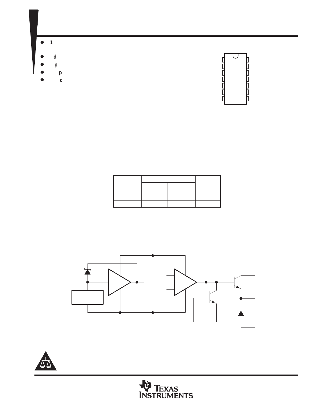
D OR N PACKAGE
(TOP VIEW)
NC
1
2
3
IN–
4
IN+
5
6
REF
CC–
7
V
NC
14
FREQ COMP
13
V
12
V
11
OUTPUT
10
9
V
8
NC
CC+
C
Z
voltage regulator, featuring high ripple rejection,
excellent input and load regulation, excellent temperature stability , and low standby current. The circuit consists
of a temperature-compensated reference-voltage amplifier, an error amplifier, a 150-mA output transistor , and
an adjustable-output current limiter.
The µA723 is designed for use in positive or negative power supplies as a series, shunt, switching, or floating
regulator. For output currents exceeding 150 mA, additional pass elements can be connected as shown in
Figures 4 and 5.
The µA723C is characterized for operation from 0°C to 70°C.
AVAILABLE OPTIONS
PACKAGED DEVICES
T
A
0°C to 70°C µA723CN µA723CD µA723Y
The D package is available taped and reeled. Add the suffix
R to the device type (e.g., µA723CDR). Chip forms are
tested at 25°C.
PLASTIC
DIP
(N)
SMALL
OUTLINE
(D)
FORM
(Y)
functional block diagram
Temperature-
Compensated
Reference Diode
Current
Source
Please be aware that an important notice concerning availability, standard warranty, and use in critical applications of
Texas Instruments semiconductor products and disclaimers thereto appears at the end of this data sheet.
PRODUCTION DATA information is current as of publication date.
Products conform to specifications per the terms of Texas Instruments
standard warranty. Production processing does not necessarily include
testing of all parameters.
Ref
Amp
V
REF
V
CC+
CC–
IN–
IN+
FREQ COMP
–
Error
Amp
+
CURR LIM CURR SENS
Copyright 1999, Texas Instruments Incorporated
Current
Limiter
V
C
Series Pass
Transistor
Regulated
Output
V
Z
POST OFFICE BOX 655303 • DALLAS, TEXAS 75265
1
µA723
PRECISION VOLTAGE REGULATORS
SLVS057D – AUGUST 1972 – REVISED JULY 1999
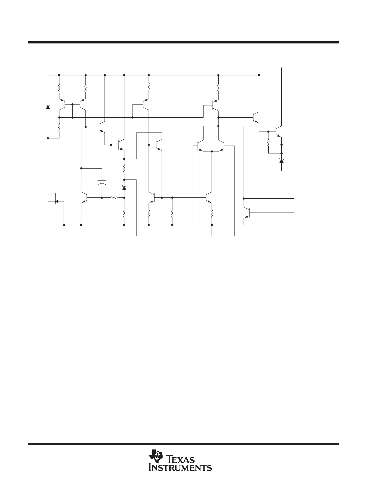
schematic
500 Ω
15 kΩ
Resistor and capacitor values shown are nominal.
25 kΩ
100 Ω
5 pF
30 kΩ
5 kΩ
1 kΩ
300 Ω
20 kΩ
V
CC–
1 kΩ
150 Ω
V
CC+
15 kΩ
IN–IN+REF
V
C
6.2 V
OUTPUT
V
Z
FREQ COMP
CURR LIM
CURR SENS
absolute maximum ratings over operating free-air temperature range (unless otherwise noted)
Peak voltage from V
Continuous voltage from V
Input-to-output voltage differential 40 V. . . . . . . . . . . . . . . . . . . . . . . . . . . . . . . . . . . . . . . . . . . . . . . . . . . . . . . . . . . .
Differential input voltage to error amplifier ±5 V. . . . . . . . . . . . . . . . . . . . . . . . . . . . . . . . . . . . . . . . . . . . . . . . . . . . .
Voltage between noninverting input and V
Current from VZ 25 mA. . . . . . . . . . . . . . . . . . . . . . . . . . . . . . . . . . . . . . . . . . . . . . . . . . . . . . . . . . . . . . . . . . . . . . . . .
Current from REF 15 mA. . . . . . . . . . . . . . . . . . . . . . . . . . . . . . . . . . . . . . . . . . . . . . . . . . . . . . . . . . . . . . . . . . . . . . . .
Package thermal impedance, θ
Lead temperature 1,6 mm (1/16 inch) from case for 10 seconds: D or N package 260°C. . . . . . . . . . . . . . . .
Storage temperature range, T
†
Stresses beyond those listed under “absolute maximum ratings” may cause permanent damage to the device. These are stress ratings only, and
functional operation of the device at these or any other conditions beyond those indicated under “recommended operating conditions” is not
implied. Exposure to absolute-maximum-rated conditions for extended periods may affect device reliability.
NOTES: 1. Maximum power dissipation is a function of TJ(max),
ambient temperature is PD = (TJ(max) – TA)/
2. The package thermal impedance is calculated in accordance with JESD 51, except for through-hole packages, which use a trace
length of zero.
CC+
to V
CC+
(tw ≤ 50 ms) 50 V. . . . . . . . . . . . . . . . . . . . . . . . . . . . . . . . . . . . . . . . . . . . . . . . .
CC–
to V
JA
40 V. . . . . . . . . . . . . . . . . . . . . . . . . . . . . . . . . . . . . . . . . . . . . . . . . . . . . . .
CC–
8 V. . . . . . . . . . . . . . . . . . . . . . . . . . . . . . . . . . . . . . . . . . . . . . . . . .
CC–
(see Notes 1 and 2): D package 86°C/W. . . . . . . . . . . . . . . . . . . . . . . . . . . .
N package 101°C/W. . . . . . . . . . . . . . . . . . . . . . . . . . .
–65°C to 150°C. . . . . . . . . . . . . . . . . . . . . . . . . . . . . . . . . . . . . . . . . . . . . . . . . . .
stg
θ
, and TA. The maximum allowable power dissipation at any allowable
θ
JA
JA
. Operating at the absolute maximum TJ of 150°C can impact reliability.
†
2
POST OFFICE BOX 655303 • DALLAS, TEXAS 75265
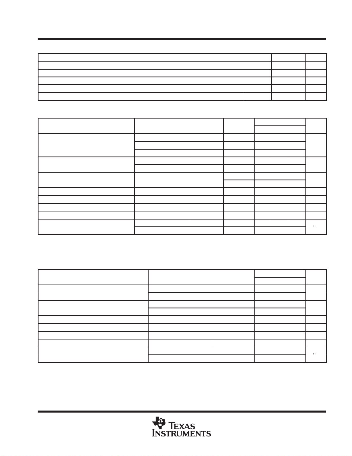
PARAMETER
TEST CONDITIONS
T
UNIT
Ripple rejection
dB
Output regulation
mV/V
Output noise voltage
V
PARAMETER
TEST CONDITIONS
UNIT
Input regulation
mV/V
Ripple rejection
dB
Output noise voltage
V
µA723
PRECISION VOLTAGE REGULATORS
SLVS057D – AUGUST 1972 – REVISED JULY 1999
recommended operating conditions
MIN MAX UNIT
Input voltage, V
Output voltage, V
Input-to-output voltage differential, VC – V
Output current, I
Operating free-air temperature range, T
I
O
O
O
A
µA723C 0 70 °C
electrical characteristics at specified free-air temperature (see Notes 3 and 4)
A
VI = 12 V to VI = 15 V 25°C 0.1 1
Input regulation
pp
p
Reference voltage, V
Standby current VI = 30 V, IO = 0 25°C 2.3 4 mA
Temperature coefficient of output voltage 0°C to 70°C 0.003 0.015 %/°C
Short-circuit output current RSC = 10 Ω, VO = 0 25°C 65 mA
p
NOTES: 3. For all values in this table, the device is connected as shown in Figure 1 with the divider resistance as seen by the error amplifier
≤ 10 kΩ. Unless otherwise specified, VI = V
4. Pulse-testing techniques must be used that will maintain the junction temperature as close to the ambient temperature as possible.
ref
VI = 12 V to VI = 40 V 25°C 1 5
VI = 12 V to VI = 15 V 0°C to 70°C 3
f = 50 Hz to 10 kHz, C
f = 50 Hz to 10 kHz, C
BW = 100 Hz to 10 kHz, C
BW = 100 Hz to 10 kHz, C
= VC = 12 V, V
CC+
= 0 25°C 74
ref
= 5 µF 25°C 86
ref
25°C –0.3 –2
0°C to 70°C –6
25°C 6.8 7.15 7.5 V
= 0 25°C 20
ref
= 5 µF 25°C 2.5
ref
= 0, VO = 5 V, IO = 1 mA, RSC = 0, and C
CC–
MIN TYP MAX
9.5 40 V
2 37 V
3 38 V
µA723C
ref
150 mA
mV/V
µ
= 0.
electrical characteristics, TA = 25°C (see Notes 3 and 4)
µA723Y
MIN TYP MAX
p
pp
Output regulation –0.3 mV/V
Reference voltage, V
Standby current VI = 30 V, IO = 0 2.3 mA
Short-circuit output current RSC = 10 Ω, VO = 0 65 mA
p
NOTES: 3. For all values in this table, the device is connected as shown in Figure 1 with the divider resistance as seen by the error amplifier
≤ 10 kΩ. Unless otherwise specified, VI = V
4. Pulse-testing techniques must be used that will maintain the junction temperature as close to the ambient temperature as possible.
ref
VI = 12 V to VI = 15 V 0.1
VI = 12 V to VI = 40 V 1
f = 50 Hz to 10 kHz, C
f = 50 Hz to 10 kHz, C
BW = 100 Hz to 10 kHz, C
BW = 100 Hz to 10 kHz, C
= VC = 12 V, V
CC+
= 0, VO = 5 V, IO = 1 mA, RSC = 0, and C
CC–
= 0 74
ref
= 5 µF 86
ref
= 0 20
ref
= 5 µF 2.5
ref
7.15 V
ref
µ
= 0.
POST OFFICE BOX 655303 • DALLAS, TEXAS 75265
3
µA723
PRECISION VOLTAGE REGULATORS
SLVS057D – AUGUST 1972 – REVISED JULY 1999
APPLICATION INFORMATION
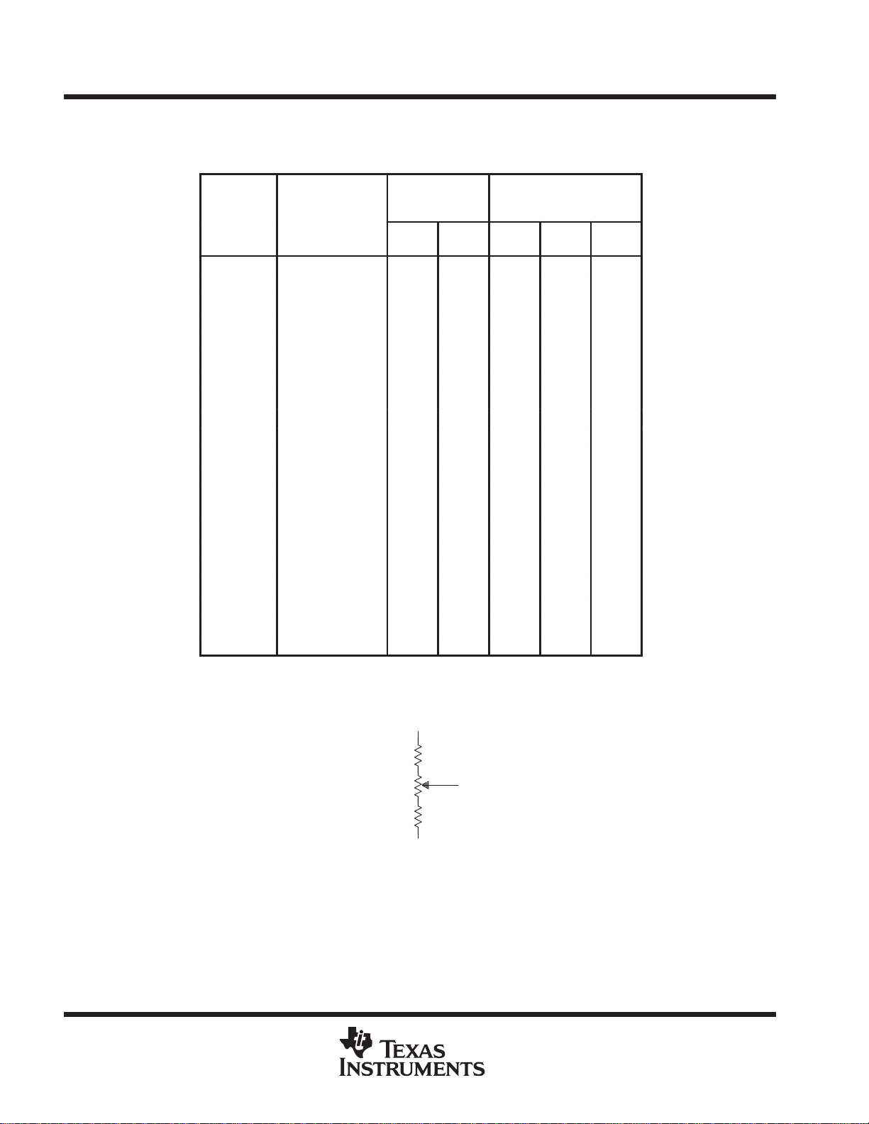
Table 1. Resistor Values (kΩ) for Standard Output Voltages
OUTPUT
VOLTAGE
(V) (SEE NOTE 5)
3.0 1, 5, 6, 9, 1 1, 12 (4) 4.12 3.01 1.8 0.5 1.2
3.6 1, 5, 6, 9, 1 1, 12 (4) 3.57 3.65 1.5 0.5 1.5
5.0 1, 5, 6, 9, 1 1, 12 (4) 2.15 4.99 0.75 0.5 2.2
6.0 1, 5, 6, 9, 1 1, 12 (4) 1.15 6.04 0.5 0.5 2.7
9.0 2, 4, (5, 6, 9, 12) 1.87 7.15 0.75 1.0 2.7
12 2, 4, (5, 6, 9, 12) 4.87 7.15 2.0 1.0 3.0
15 2, 4, (5, 6, 9, 12) 7.87 7.15 3.3 1.0 3.0
28 2, 4, (5, 6, 9, 12) 21.0 7.15 5.6 1.0 2.0
45 7 3.57 48.7 2.2 10 39
75 7 3.57 78.7 2.2 10 68
100 7 3.57 105 2.2 10 91
250 7 3.57 255 2.2 10 240
–6
(see Note 7)
–9 3, 10 3.48 5.36 1.2 0.5 2.0
–12 3, 10 3.57 8.45 1.2 0.5 3.3
–15 3, 10 3.57 11.5 1.2 0.5 4.3
–28 3, 10 3.57 24.3 1.2 0.5 10
–45 8 3.57 41.2 2.2 10 33
–100 8 3.57 95.3 2.2 10 91
–250 8 3.57 249 2.2 10 240
NOTES: 5. The R1/R2 divider can be across either VO or V
APPLICABLE
FIGURES
3, 10 3.57 2.43 1.2 0.5 0.75
V
, use the figure numbers without parentheses. If the divider is across
(ref)
VO, use the figure numbers in parentheses.
6. T o make the voltage adjustable, the R1/R2 divider shown in the figures must
be replaced by the divider shown below.
FIXED OUTPUT
±5%
R1
(kΩ)R2(kΩ)R1(kΩ)P1(kΩ )P2(kΩ )
OUTPUT ADJUSTABLE
(ref)
±10%
(SEE NOTE 6)
. If the divider is across
R1
P1
R2
Adjustable Output Circuit
7. For Figures 3, 8, and 10, the device requires a minimum of 9 V between V
and V
4
when VO is equal to or more positive than –9 V.
CC–
POST OFFICE BOX 655303 • DALLAS, TEXAS 75265
CC+

µA723
PRECISION VOLTAGE REGULATORS
SLVS057D – AUGUST 1972 – REVISED JULY 1999
APPLICATION INFORMATION
Table 2. Formulas for Intermediate Output Voltages
OUTPUTS FROM 2 V TO 7 V
SEE FIGURES 1, 5, 6, 9, 11, 12 (4)
AND NOTE 5
VO+
V
(
ref
)
R2
R1)R2
OUTPUTS FROM 7 V TO 37 V
OUTPUTS FROM 4 V TO 250 V
SEE FIGURE 7 AND NOTE 5
VO+
R3+R4
OUTPUTS FROM –6 V TO –250 V
SEE FIGURES 2, 4, (5, 6, 9, 11, 12)
AND NOTE 5
VO+
V
R1)R2
(
)
ref
R2
VO+
R3+R4
NOTES: 5. The R1/R2 divider can be across either VO or V
divider is across VO, use the figure numbers in parentheses.
7. For Figures 3, 8, and 10, the device requires a minimum of 9 V between V
–9 V.
V
REF
R1
IN+
C
(ref)
V
CC–
R2
V
(
)
ref
R2–R1
2
R1
SEE FIGURES 3, 8, 10
AND NOTES 5 AND 7
V
(
)
ref
–
. If the divider is across V
(ref)
V
I
CC+
R1)R2
2
V
C
R1
OUTPUT
µA723
V
Z
CURR LIM
CURR SENS
IN–
FREQ COMP
FOLDBACK CURRENT LIMITING
I
(knee)
IOS[
, use figure numbers without parentheses. If the
(ref)
R
CC+
SC
and V
when VO is equal to or more positive than
CC–
Regulated
Output, V
O
R3 (see Notes A and B)
100 pF
CURRENT LIMITING
0.65 V
I
[
(limit)
R
SC
SEE FIGURE 6
V
R3)(R3)R4) 0.65 V
O
[
0.65 V
R
SC
R
SC
R3)R4
R4
R4
NOTES: A.
R1 R2
R3
+
B. R3 can be eliminated for minimum component count. Use direct connection (i.e., R3 = 0).
R1)R2
for a minimum
a
V
O
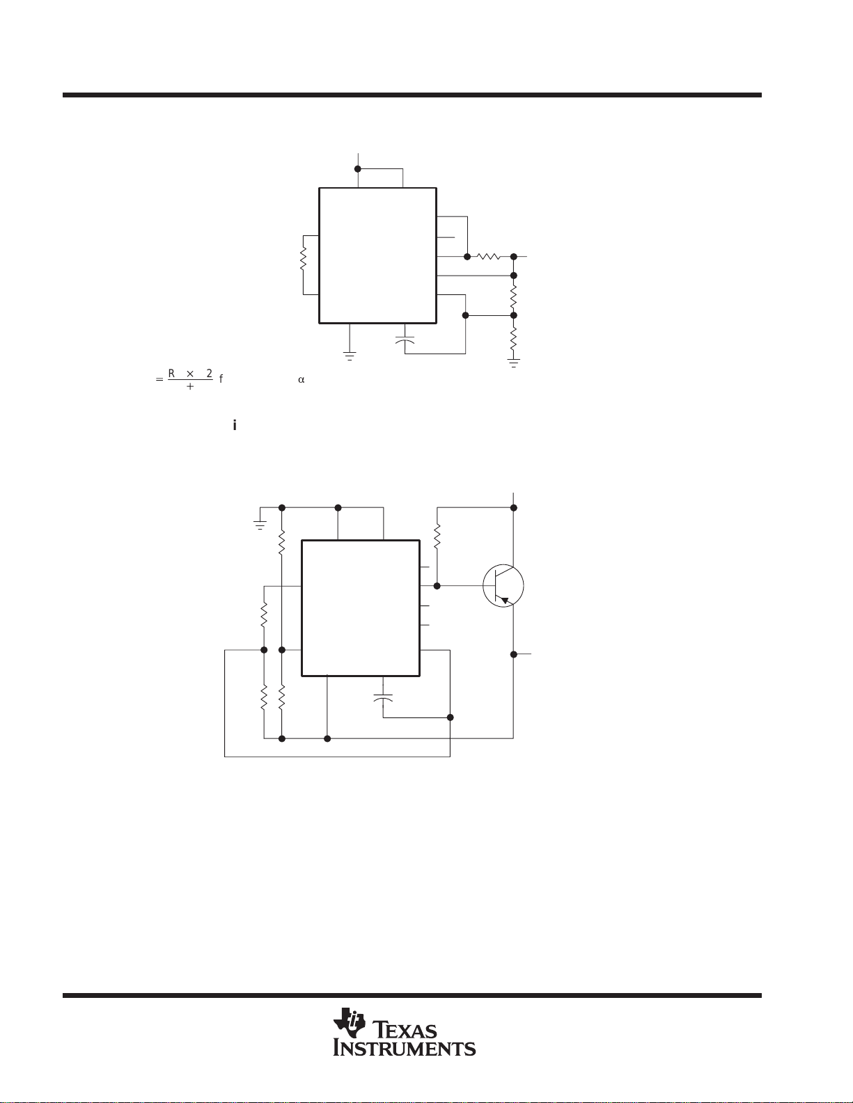
Figure 1. Basic Low-Voltage Regulator (VO = 2 V to 7 V)
POST OFFICE BOX 655303 • DALLAS, TEXAS 75265
5
µA723
PRECISION VOLTAGE REGULATORS
SLVS057D – AUGUST 1972 – REVISED JULY 1999
APPLICATION INFORMATION
V
I
NOTES: A.
B. R3 can be eliminated for minimum component count. Use direct connection (i.e., R3 = 0).
R3
(see Notes A and B)
R1 R2
+
R1)R2
R4 = 3 kΩ
V
CC+
OUTPUT
µA723
CURR LIM
CURR SENS
FREQ COMP
C
V
Z
IN–
100 pF
R
SC
Regulated Output,
V
O
R1
R2
R3
for a minimum
V
REF
IN+
V
CC–
a
V
O
Figure 2. Basic High-Voltage Regulator (VO = 7 V to 37 V)
V
I
2 kΩ
Z
2N5001
Regulated Output,
V
O
R3 =
3 kΩ
R2
R1
REF
IN+
V
CC–
V
CC+
µA723
CURR LIM
CURR SENS
FREQ COMP
V
C
OUTPUT
V
IN–
100 pF
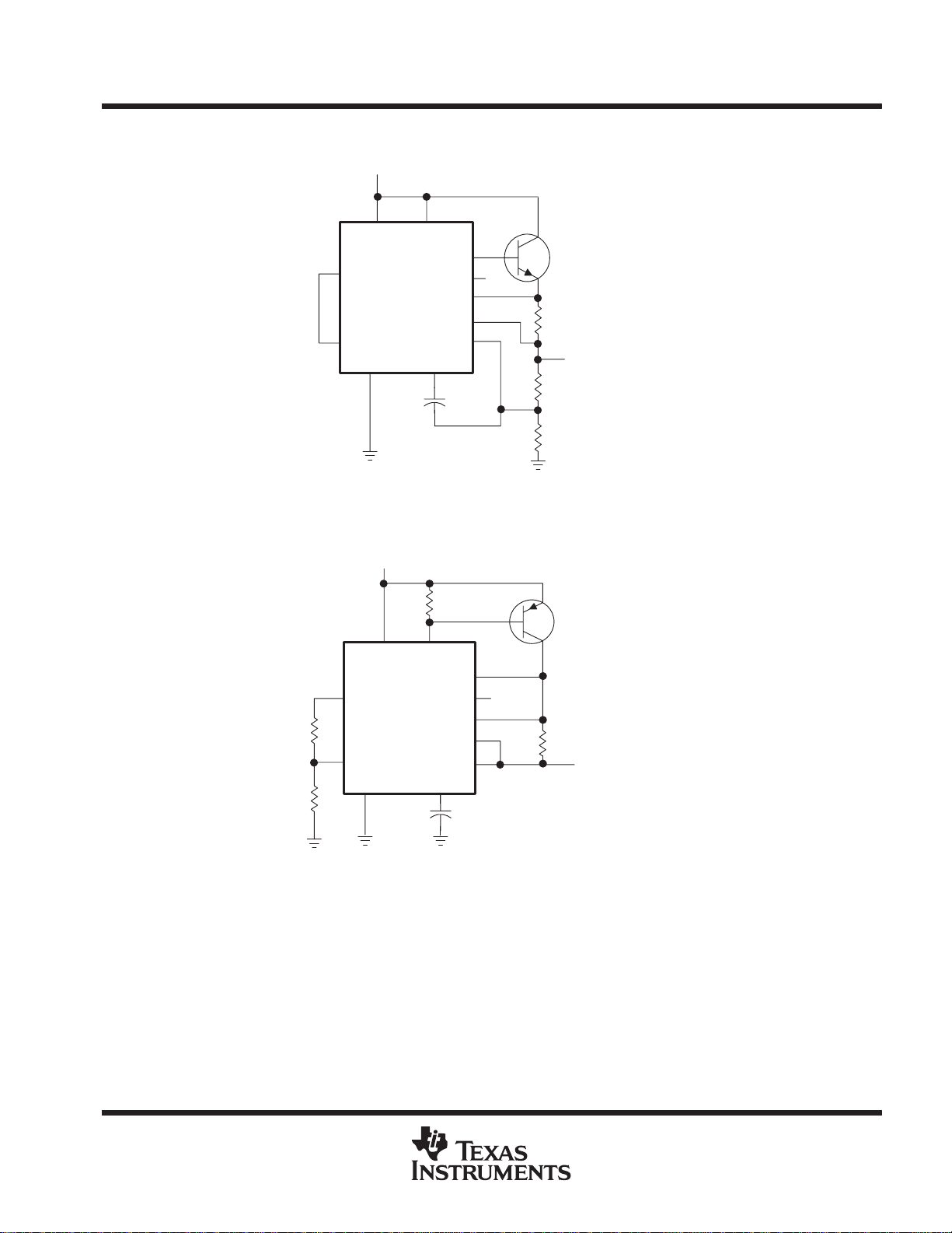
Figure 3. Negative-Voltage Regulator
6
POST OFFICE BOX 655303 • DALLAS, TEXAS 75265
µA723
PRECISION VOLTAGE REGULATORS
SLVS057D – AUGUST 1972 – REVISED JULY 1999
APPLICATION INFORMATION
V
I
V
C
OUTPUT
µA723
CURR SENS
FREQ COMP
V
CURR LIM
IN–
500 pF
2N3997
Z
R
SC
Regulated Output,
V
O
R1
R2
REF
IN+
V
CC–
V
CC+
Figure 4. Positive-Voltage Regulator (External npn Pass Transistor)
V
I
60 Ω
2N5001
V
C
OUTPUT
µA723
CURR LIM
CURR SENS
FREQ COMP
V
Z
IN–
1000 pF
R
SC
Regulated Output,
V
O
R1
R2
REF
IN+
V
CC–
V
CC+
Figure 5. Positive-Voltage Regulator (External pnp Pass Transistor)
POST OFFICE BOX 655303 • DALLAS, TEXAS 75265
7

µA723
PRECISION VOLTAGE REGULATORS
SLVS057D – AUGUST 1972 – REVISED JULY 1999
APPLICATION INFORMATION
V
I
V
OUTPUT
µA723
CURR LIM
CURR SENS
FREQ COMP
C
V
Z
IN–
1000 pF
R1
R2
REF
IN+
V
V
CC–
CC+
Figure 6. Foldback Current Limiting
V
C
OUTPUT
µA723
CURR LIM
CURR SENS
FREQ COMP
V
IN–
500 pF
1N1826
R4 =
3 kΩ
R3 =
3 kΩ
R1
R2
V
REF
IN+
V
CC–
CC+
R
SC
Regulated Output,
V
R3
R4
2 kΩ
Z
O
I
OS
V
O
V
I
2N2580
RSC = 1 Ω
Regulated Output,
V
O
I
O
l
knee
Figure 7. Positive Floating Regulator
8
POST OFFICE BOX 655303 • DALLAS, TEXAS 75265

µA723
PRECISION VOLTAGE REGULATORS
SLVS057D – AUGUST 1972 – REVISED JULY 1999
APPLICATION INFORMATION
V
10 kΩ
I
0.1 µF
R1
R2
R2
R1
1 kΩ
V
C
OUTPUT
µA723
CURR LIM
CURR SENS
FREQ COMP
V
Z
IN–
500 pF
10 kΩ
1N759
R3 =
3 kΩ
REF
IN+
V
R4 =
3 kΩ
V
CC–
CC+
Figure 8. Negative Floating Regulator
V
I
3 kΩ
2N5005
V
C
OUTPUT
µA723
CURR LIM
CURR SENS
IN–
FREQ COMP
V
Z
51 Ω
1N4005
1 MΩ
REF
IN+
V
V
CC–
CC+
2N5287
Regulated Output,
V
O
2N5153
L = 1.2 mH
(see Note A)
Regulated Output,
V
O
NOTE A: L is 40 turns of No. 20 enameled copper wire wound on Ferroxcube P36/22-3B7 potted core, or equivalent, with a 0.009-inch air gap.
Figure 9. Positive Switching Regulator
POST OFFICE BOX 655303 • DALLAS, TEXAS 75265
9

µA723
PRECISION VOLTAGE REGULATORS
SLVS057D – AUGUST 1972 – REVISED JULY 1999
APPLICATION INFORMATION
V
I
(see Note A)
V
REF
IN+
V
1N4005
CC+
µA723
CC–
CURR LIM
CURR SENS
FREQ COMP
R2
0.1 µF
1 kΩ
R1
NOTES: A. The device requires a minimum of 9 V between V
B. L is 40 turns of No. 20 enameled copper wire wound on Ferroxcube P36/22-3B7 potted core, or equivalent, with a 0.009-inch
air gap.
1 MΩ
V
C
OUTPUT
V
IN–
and V
CC+
Z
15 pF
R3 =
3 kΩ
R4 =
3 kΩ
100 µF
when VO is equal to or more positive than –9 V.
CC–
1 kΩ
220 Ω
2N5004
L = 1.2 mH
(see Note B)
Regulated Output,
V
O
2N3997
Figure 10. Negative Switching Regulator
V
I
V
CC+
REF
R1
IN+
V
CC–
R2
NOTE A: A current-limiting transistor can be used for shutdown if current limiting is not required.
V
C
OUTPUT
µA723
CURR LIM
CURR SENS
FREQ COMP
V
Z
IN–
1000 pF
2 kΩ
R
SC
2N4422
Regulated Output,
V
O
2 kΩ
Input From
Series 54/74 Logic
Figure 11. Remote Shutdown Regulator With Current Limiting
10
POST OFFICE BOX 655303 • DALLAS, TEXAS 75265

µA723
PRECISION VOLTAGE REGULATORS
SLVS057D – AUGUST 1972 – REVISED JULY 1999
APPLICATION INFORMATION
V
I
R1
REF
IN+
V
V
CC–
CC+
µA723
V
C
OUTPUT
V
CURR LIM
CURR SENS
IN–
FREQ COMP
5000 pF
Figure 12. Shunt Regulator
100 Ω
Z
1 kΩ
R2
2N3997
Regulated Output,
V
O
POST OFFICE BOX 655303 • DALLAS, TEXAS 75265
11

IMPORTANT NOTICE
Texas Instruments Incorporated and its subsidiaries (TI) reserve the right to make corrections, modifications, enhancements,
improvements, and other changes to its products and services at any time and to discontinue any product or service without notice.
Customers should obtain the latest relevant information before placing orders and should verify that such information is current and
complete. All products are sold subject to TI’s terms and conditions of sale supplied at the time of order acknowledgment.
TI warrants performance of its hardware products to the specifications applicable at the time of sale in accordance with TI’s
standard warranty. Testing and other quality control techniques are used to the extent TI deems necessary to support this
warranty. Except where mandated by government requirements, testing of all parameters of each product is not necessarily
performed.
TI assumes no liability for applications assistance or customer product design. Customers are responsible for their products and
applications using TI components. To minimize the risks associated with customer products and applications, customers should
provide adequate design and operating safeguards.
TI does not warrant or represent that any license, either express or implied, is granted under any TI patent right, copyright, mask
work right, or other TI intellectual property right relating to any combination, machine, or process in which TI products or services
are used. Information published by TI regarding third-party products or services does not constitute a license from TI to use such
products or services or a warranty or endorsement thereof. Use of such information may require a license from a third party under
the patents or other intellectual property of the third party, or a license from TI under the patents or other intellectual property of TI.
Reproduction of information in TI data books or data sheets is permissible only if reproduction is without alteration and is
accompanied by all associated warranties, conditions, limitations, and notices. Reproduction of this information with alteration is an
unfair and deceptive business practice. TI is not responsible or liable for such altered documentation.
Resale of TI products or services with statements different from or beyond the parameters stated by TI for that product or service
voids all express and any implied warranties for the associated TI product or service and is an unfair and deceptive business
practice. TI is not responsible or liable for any such statements.
TI products are not authorized for use in safety-critical applications (such as life support) where a failure of the TI product would
reasonably be expected to cause severe personal injury or death, unless officers of the parties have executed an agreement
specifically governing such use. Buyers represent that they have all necessary expertise in the safety and regulatory ramifications
of their applications, and acknowledge and agree that they are solely responsible for all legal, regulatory and safety-related
requirements concerning their products and any use of TI products in such safety-critical applications, notwithstanding any
applications-related information or support that may be provided by TI. Further, Buyers must fully indemnify TI and its
representatives against any damages arising out of the use of TI products in such safety-critical applications.
TI products are neither designed nor intended for use in military/aerospace applications or environments unless the TI products are
specifically designated by TI as military-grade or "enhanced plastic." Only products designated by TI as military-grade meet military
specifications. Buyers acknowledge and agree that any such use of TI products which TI has not designated as military-grade is
solely at the Buyer's risk, and that they are solely responsible for compliance with all legal and regulatory requirements in
connection with such use.
TI products are neither designed nor intended for use in automotive applications or environments unless the specific TI products
are designated by TI as compliant with ISO/TS 16949 requirements. Buyers acknowledge and agree that, if they use any
non-designated products in automotive applications, TI will not be responsible for any failure to meet such requirements.
Following are URLs where you can obtain information on other Texas Instruments products and application solutions:
Products Applications
Amplifiers amplifier.ti.com Audio www.ti.com/audio
Data Converters dataconverter.ti.com Automotive www.ti.com/automotive
DSP dsp.ti.com Broadband www.ti.com/broadband
Interface interface.ti.com Digital Control www.ti.com/digitalcontrol
Logic logic.ti.com Military www.ti.com/military
Power Mgmt power.ti.com Optical Networking www.ti.com/opticalnetwork
Microcontrollers microcontroller.ti.com Security www.ti.com/security
Low Power www.ti.com/lpw Telephony www.ti.com/telephony
Wireless
Video & Imaging www.ti.com/video
Wireless www.ti.com/wireless
Mailing Address: Texas Instruments, Post Office Box 655303, Dallas, Texas 75265
Copyright © 2007, Texas Instruments Incorporated

PACKAGE OPTION ADDENDUM
www.ti.com
4-Jun-2007
PACKAGING INFORMATION
Orderable Device Status
(1)
Package
Type
Package
Drawing
Pins Package
Qty
Eco Plan
UA723CD ACTIVE SOIC D 14 50 Green (RoHS &
no Sb/Br)
UA723CDE4 ACTIVE SOIC D 14 50 Green (RoHS &
no Sb/Br)
UA723CDG4 ACTIVE SOIC D 14 50 Green (RoHS &
no Sb/Br)
UA723CDR ACTIVE SOIC D 14 2500 Green (RoHS &
no Sb/Br)
UA723CDRE4 ACTIVE SOIC D 14 2500 Green (RoHS &
no Sb/Br)
UA723CDRG4 ACTIVE SOIC D 14 2500 Green (RoHS &
no Sb/Br)
UA723CJ OBSOLETE CDIP J 14 TBD Call TI Call TI
UA723CN ACTIVE PDIP N 14 25 Pb-Free
UA723CNE4 ACTIVE PDIP N 14 25 Pb-Free
UA723CNSR ACTIVE SO NS 14 2000 Green (RoHS &
no Sb/Br)
UA723CNSRE4 ACTIVE SO NS 14 2000 Green (RoHS &
no Sb/Br)
UA723CNSRG4 ACTIVE SO NS 14 2000 Green (RoHS &
no Sb/Br)
(1)
The marketing status values are defined as follows:
ACTIVE: Product device recommended for new designs.
LIFEBUY: TI has announced that the device will be discontinued, and a lifetime-buy period is in effect.
NRND: Not recommended for new designs. Device is in production to support existing customers, but TI does not recommend using this part in
a new design.
PREVIEW: Device has been announced but is not in production. Samples may or may not be available.
OBSOLETE: TI has discontinued the production of the device.
(RoHS)
(RoHS)
(2)
Lead/Ball Finish MSL Peak Temp
CU NIPDAU Level-1-260C-UNLIM
CU NIPDAU Level-1-260C-UNLIM
CU NIPDAU Level-1-260C-UNLIM
CU NIPDAU Level-1-260C-UNLIM
CU NIPDAU Level-1-260C-UNLIM
CU NIPDAU Level-1-260C-UNLIM
CU NIPDAU N / A for Pkg Type
CU NIPDAU N / A for Pkg Type
CU NIPDAU Level-1-260C-UNLIM
CU NIPDAU Level-1-260C-UNLIM
CU NIPDAU Level-1-260C-UNLIM
(3)
(2)
Eco Plan - The planned eco-friendly classification: Pb-Free (RoHS), Pb-Free (RoHS Exempt), or Green (RoHS & no Sb/Br) - please check
http://www.ti.com/productcontent for the latest availability information and additional product content details.
TBD: The Pb-Free/Green conversion plan has not been defined.
Pb-Free (RoHS): TI's terms "Lead-Free" or "Pb-Free" mean semiconductor products that are compatible with the current RoHS requirements
for all 6 substances, including the requirement that lead not exceed 0.1% by weight in homogeneous materials. Where designed to be soldered
at high temperatures, TI Pb-Free products are suitable for use in specified lead-free processes.
Pb-Free (RoHS Exempt): This component has a RoHS exemption for either 1) lead-based flip-chip solder bumps used between the die and
package, or 2) lead-based die adhesive used between the die and leadframe. The component is otherwise considered Pb-Free (RoHS
compatible) as defined above.
Green (RoHS & no Sb/Br): TI defines "Green" to mean Pb-Free (RoHS compatible), and free of Bromine (Br) and Antimony (Sb) based flame
retardants (Br or Sb do not exceed 0.1% by weight in homogeneous material)
(3)
MSL, Peak Temp. -- The Moisture Sensitivity Level rating according to the JEDEC industry standard classifications, and peak solder
temperature.
Important Information and Disclaimer:The information provided on this page represents TI's knowledge and belief as of the date that it is
provided. TI bases its knowledge and belief on information provided by third parties, and makes no representation or warranty as to the
accuracy of such information. Efforts are underway to better integrate information from third parties. TI has taken and continues to take
reasonable steps to provide representative and accurate information but may not have conducted destructive testing or chemical analysis on
incoming materials and chemicals. TI and TI suppliers consider certain information to be proprietary, and thus CAS numbers and other limited
information may not be available for release.
Addendum-Page 1

PACKAGE OPTION ADDENDUM
www.ti.com
In no event shall TI's liability arising out of such information exceed the total purchase price of the TI part(s) at issue in this document sold by TI
to Customer on an annual basis.
4-Jun-2007
Addendum-Page 2

PACKAGE MATERIALS INFORMATION
www.ti.com
TAPE AND REEL INFORMATION
11-Mar-2008
*All dimensions are nominal
Device Package
UA723CDR SOIC D 14 2500 330.0 16.4 6.5 9.0 2.1 8.0 16.0 Q1
UA723CNSR SO NS 14 2000 330.0 16.4 8.2 10.5 2.5 12.0 16.0 Q1
Type
Package
Drawing
Pins SPQ Reel
Diameter
(mm)
Reel
Width
W1 (mm)
A0 (mm) B0 (mm) K0 (mm) P1
(mm)W(mm)
Pin1
Quadrant
Pack Materials-Page 1

PACKAGE MATERIALS INFORMATION
www.ti.com
11-Mar-2008
*All dimensions are nominal
Device Package Type Package Drawing Pins SPQ Length (mm) Width (mm) Height (mm)
UA723CDR SOIC D 14 2500 346.0 346.0 33.0
UA723CNSR SO NS 14 2000 346.0 346.0 33.0
Pack Materials-Page 2


IMPORTANT NOTICE
Texas Instruments Incorporated and its subsidiaries (TI) reserve the right to make corrections, modifications, enhancements, improvements,
and other changes to its products and services at any time and to discontinue any product or service without notice. Customers should
obtain the latest relevant information before placing orders and should verify that such information is current and complete. All products are
sold subject to TI’s terms and conditions of sale supplied at the time of order acknowledgment.
TI warrants performance of its hardware products to the specifications applicable at the time of sale in accordance with TI’s standard
warranty. Testing and other quality control techniques are used to the extent TI deems necessary to support this warranty. Except where
mandated by government requirements, testing of all parameters of each product is not necessarily performed.
TI assumes no liability for applications assistance or customer product design. Customers are responsible for their products and
applications using TI components. To minimize the risks associated with customer products and applications, customers should provide
adequate design and operating safeguards.
TI does not warrant or represent that any license, either express or implied, is granted under any TI patent right, copyright, mask work right,
or other TI intellectual property right relating to any combination, machine, or process in which TI products or services are used. Information
published by TI regarding third-party products or services does not constitute a license from TI to use such products or services or a
warranty or endorsement thereof. Use of such information may require a license from a third party under the patents or other intellectual
property of the third party, or a license from TI under the patents or other intellectual property of TI.
Reproduction of TI information in TI data books or data sheets is permissible only if reproduction is without alteration and is accompanied
by all associated warranties, conditions, limitations, and notices. Reproduction of this information with alteration is an unfair and deceptive
business practice. TI is not responsible or liable for such altered documentation. Information of third parties may be subject to additional
restrictions.
Resale of TI products or services with statements different from or beyond the parameters stated by TI for that product or service voids all
express and any implied warranties for the associated TI product or service and is an unfair and deceptive business practice. TI is not
responsible or liable for any such statements.
TI products are not authorized for use in safety-critical applications (such as life support) where a failure of the TI product would reasonably
be expected to cause severe personal injury or death, unless officers of the parties have executed an agreement specifically governing
such use. Buyers represent that they have all necessary expertise in the safety and regulatory ramifications of their applications, and
acknowledge and agree that they are solely responsible for all legal, regulatory and safety-related requirements concerning their products
and any use of TI products in such safety-critical applications, notwithstanding any applications-related information or support that may be
provided by TI. Further, Buyers must fully indemnify TI and its representatives against any damages arising out of the use of TI products in
such safety-critical applications.
TI products are neither designed nor intended for use in military/aerospace applications or environments unless the TI products are
specifically designated by TI as military-grade or "enhanced plastic." Only products designated by TI as military-grade meet military
specifications. Buyers acknowledge and agree that any such use of TI products which TI has not designated as military-grade is solely at
the Buyer's risk, and that they are solely responsible for compliance with all legal and regulatory requirements in connection with such use.
TI products are neither designed nor intended for use in automotive applications or environments unless the specific TI products are
designated by TI as compliant with ISO/TS 16949 requirements. Buyers acknowledge and agree that, if they use any non-designated
products in automotive applications, TI will not be responsible for any failure to meet such requirements.
Following are URLs where you can obtain information on other Texas Instruments products and application solutions:
Products Applications
Amplifiers amplifier.ti.com Audio www.ti.com/audio
Data Converters dataconverter.ti.com Automotive www.ti.com/automotive
DSP dsp.ti.com Broadband www.ti.com/broadband
Clocks and Timers www.ti.com/clocks Digital Control www.ti.com/digitalcontrol
Interface interface.ti.com Medical www.ti.com/medical
Logic logic.ti.com Military www.ti.com/military
Power Mgmt power.ti.com Optical Networking www.ti.com/opticalnetwork
Microcontrollers microcontroller.ti.com Security www.ti.com/security
RFID www.ti-rfid.com Telephony www.ti.com/telephony
RF/IF and ZigBee® Solutions www.ti.com/lprf Video & Imaging www.ti.com/video
Mailing Address: Texas Instruments, Post Office Box 655303, Dallas, Texas 75265
Copyright © 2008, Texas Instruments Incorporated
Wireless www.ti.com/wireless
 Loading...