

Page 1

Philips Semiconductors
µA733/733C
Differential video amplifier
Product specification April 15, 1992
LINEAR PRODUCTS
IC11
Page 2
Philips Semiconductors Product specification
µA733/733CDifferential video amplifier
2
1992 Apr 15 853-1064 06456
DESCRIPTION
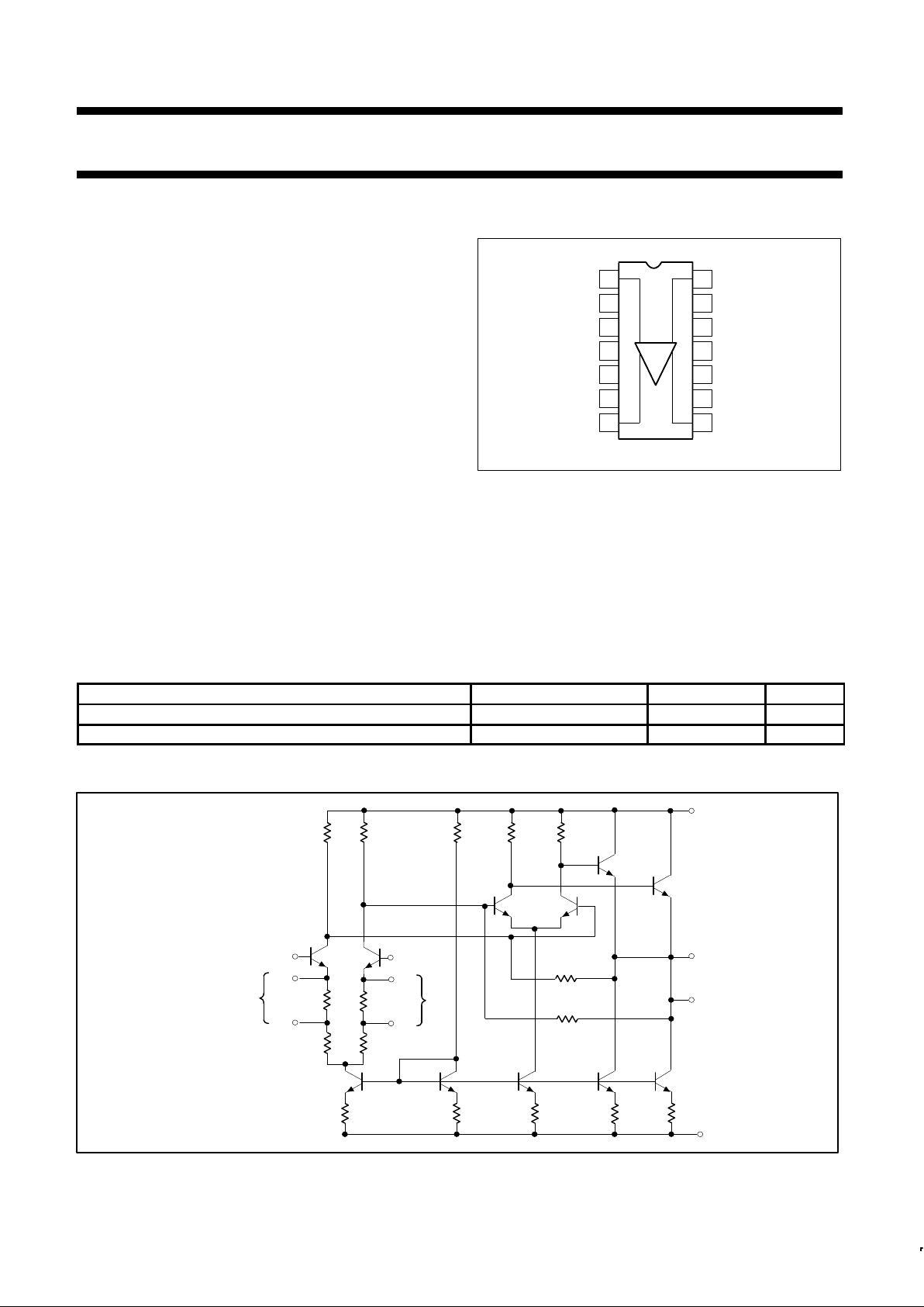
The 733 is a monolithic differential input, differential output,
wide-band video amplifier. It offers fixed gains of 10, 100, or 400
without external components, and adjustable gains from 10 to 400
by the use of an external resistor. No external frequency
compensation components are required for any gain option. Gain
stability, wide bandwidth, and low phase distortion are obtained
through use of the classic series-shunt feedback from the
emitter-follower outputs to the inputs of the second stage. The
emitter-follower outputs provide low output impedance, and enable
the device to drive capacitive loads. The 733 is intended for use as
a high-performance video and pulse amplifier in communications,
magnetic memories, display and video recorder systems.
FEA TURES
•120MHz bandwidth
•250kΩ input resistance
•Selectable gains of 10, 100, and 400
•No frequency compensation required
•MIL-STD-883A, B, C available
PIN CONFIGURA TION
1
2
3
4
5
6
78
14
13
12
11
10
9
INPUT 2
NC
V–
NC
OUTPUT 2
INPUT 1
NC
V+
NC
OUTPUT 1
TOP VIEW
N Package
G
2B
GAIN SELECT
G
1B
GAIN SELECT
G
2A
GAIN SELECT
G
1A
GAIN SELECT
SL00089
Figure 1. Pin Configuration
APPLICATIONS
•Video amplifier
•Pulse amplifier in communications
•Magnetic memories
•Video recorder systems
ORDERING INFORMATION
DESCRIPTION TEMPERATURE ORDER CODE DWG #
14-Pin Plastic Dual In–Line Package (DIP) -55°C to +125°C µA733N SOT27-1
14-Pin Plastic Dual In–Line Package (DIP) 0 to +70°C µA733CN SOT27-1
CIRCUIT SCHEMA TIC
+V
Q6
OUTPUT 1
OUTPUT 2
R1
R2 R8 R10 R9
Q5
Q4
Q3
R12
Q11
R14
Q9
G
1A
INPUT 1
INPUT 2
R3 R5
Q1
Q2
-V
2.4kΩ
2.4kΩ
G
2A
GAIN
SELECT
50Ω
590Ω
50Ω
R4
590Ω
R6
Q7
R7
300Ω
G
2B
G
1B
10kΩ
1.1kΩ
1.1kΩ
R11
7kΩ
7kΩ
1.4kΩ
Q8 Q10
300Ω
R12
400Ω
400Ω
SP00090
Figure 2. Circuit Schematic
Page 3
Philips Semiconductors Product specification
µA733/733CDifferential video amplifier
1992 Apr 15
3
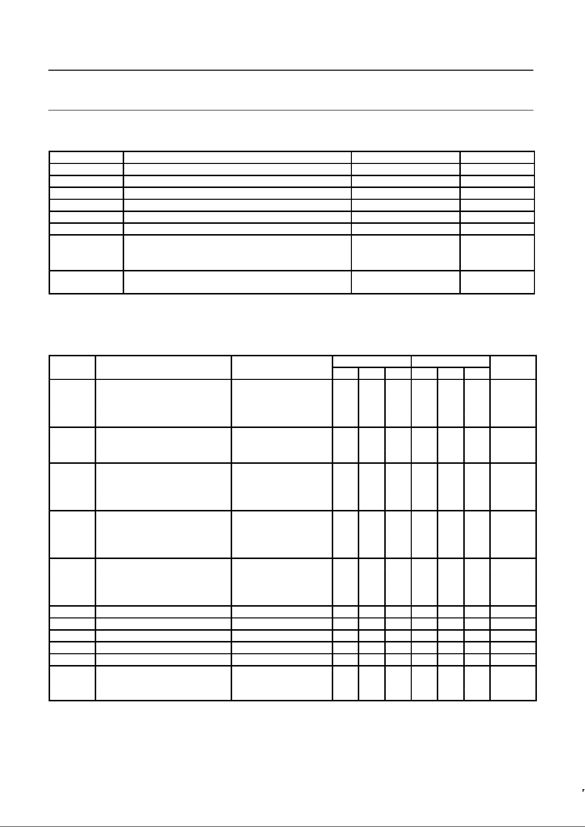
ABSOLUTE MAXIMUM RATINGS
SYMBOL PARAMETER RATING UNIT
V
DIFF
Differential input voltage ±5 V
V
CM
Common-mode input voltage ±6 V
V
CC
Supply voltage ±8 V
I
OUT
Output current 10 mA
T
J
Junction temperature +150 °C
T
STG
Storage temperature range -65 to +150 °C
T
A
Operating ambient temperature range
µA733C 0 to +70 °C
µA733 -55 to +125 °C
P
D MAX
Maximum power dissipation, 1420 mW
25°C ambient temperature (still-air)
1
NOTE:
1. The following derating factors should be applied above 25°C:
N package at 11.4mW/°C
DC ELECTRICAL CHARACTERISTICS
TA=+25°C, VS=±6V, VCM=0, unless otherwise specified. Recommended operating supply voltages VS=±6.0V.
µA733C µA733
SYMBOL
PARAMETER
TEST CONDITIONS
Min Typ Max Min Typ Max
UNIT
Differential voltage gain RI = 2kΩ, V
OUT
= 3V
P-P
Gain 1
2
250 400 600 300 400 500 V/V
Gain 2
2
80 100 120 90 100 110 V/V
Gain 3
3
8 10 12 9 10 11 V/V
Gain 1
1
40 40
BW Gain 2
2
90 90 MHz
Gain 3
3
120 120
t
R
V
OUT
= 1V
P-P
Gain 1
1
10.5 10.5 ns
Gain 2
2
4.5 12 4.5 10 ns
Gain 3
3
2.5 2.5 ns
t
PD
V
OUT
= 1V
P-P
Gain 1
1
7.5 7.5 ns
Gain 2
2
6.0 10 6.0 10 ns
Gain 3
3
3.6 3.6 ns
R
IN
Gain 1
2
4.0 4.0 kΩ
Gain 2
2
10 30 20 30 kΩ
Gain 3
3
250 250 kΩ
Input capacitance
2
Gain 2 2.0 2.0 pF
I
OS
Input offset current 0.4 5.0 0.4 3.0 µA
I
BIAS
Input bias current 9.0 30 9.0 20 µA
V
NOISE
Input noise voltage BW=1kHz to 10MHz 12 12 µV
RMS
V
IN
Input voltage range ±1.0 ±1.0 V
CMRR
Gain 2 VCM=±1V, f≤100kHz 60 86 60 86 dB
Gain 2 VCM=±1V, f=5MHz 60 60 dB
Page 4
Philips Semiconductors Product specification
µA733/733CDifferential video amplifier
1992 Apr 15
4
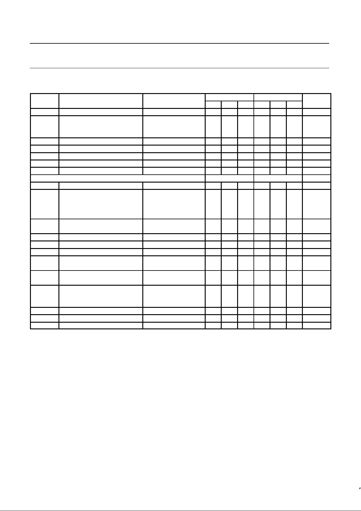
DC ELECTRICAL CHARACTERISTICS (Continued)
µA733C µA733
SYMBOL
PARAMETER
TEST CONDITIONS
Min Typ Max Min Typ Max
UNIT
SVRR Supply voltage rejection ratio Gain 2 ∆V
S
= ±0.5V 50 70 50 70 dB
Output offset voltage R
L
= ∞
Gain 1
1
0.6 1.5 0.6 1.5 V
Gain 2 and 3
2, 3
0.35 1.5 0.35 1.0 V
V
CM
Output common-mode voltage R
L
= ∞ 2.4 2.9 3.4 2.4 2.9 3.4 V
Output voltage swing, differential RL=2kΩ 3.0 4.0 3.0 4.0 V
P-P
I
SINK
Output sink current 2.5 3.6 2.5 3.6 mA
R
OUT
Output resistance 20 20 Ω
I
CC
Power supply current R
L
= ∞ 18 24 18 24 mA
THE FOLLOWING SPECIFICATIONS APPLY OVER TEMPERATURE 0°C ≤ T
A
≤ 70°C -55°C ≤ T
A
≤ 125°C
Min Typ Max Min Typ Max UNIT
Differential voltage gain RI = 2kΩ, V
OUT
= 3V
P-P
Gain 1
1
250 600 200 600 V/V
Gain 2
2
80 120 80 120 V/V
Gain
3
8 12 8 12 V/V
R
IN
Input resistance
Gain 2
2
8 8 kΩ
I
OS
Input offset current 6 5 µA
I
BIAS
Input bias current 40 40 µA
V
IN
Input voltage range ±1.0 ±1.0 V
CMRR Common-mode rejection ratio
Gain 2 VCM=±V, F≤100kHz 50 50 dB
SVRR Supply voltage rejection ratio
Gain 2 ∆VS=±0.5V 50 50 dB
V
OS
Output offset voltage R
L
= ∞
Gain 1
1
1.5 1.5 V
Gain 2 and 3
2, 3
1.5 1.2 V
V
DIFF
Output voltage swing, differential R
L
= 2kΩ 2.8 2.5 V
P-P
I
SINK
Output sink current 2.5 2.2 mA
I
CC
Power supply current R
L
±∞ 27 27 mA
NOTES:
1. Gain select pins G
1A
and G1B connected together.
2. Gain select pins G
2A
and G2B connected together.
3. All gain select pins open.
Page 5
Philips Semiconductors Product specification
µA733/733CDifferential video amplifier
1992 Apr 15
5
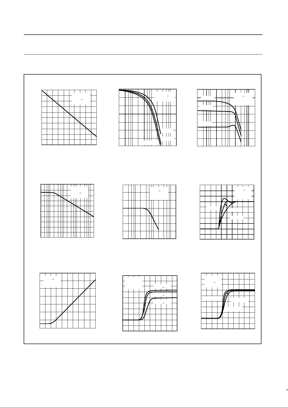
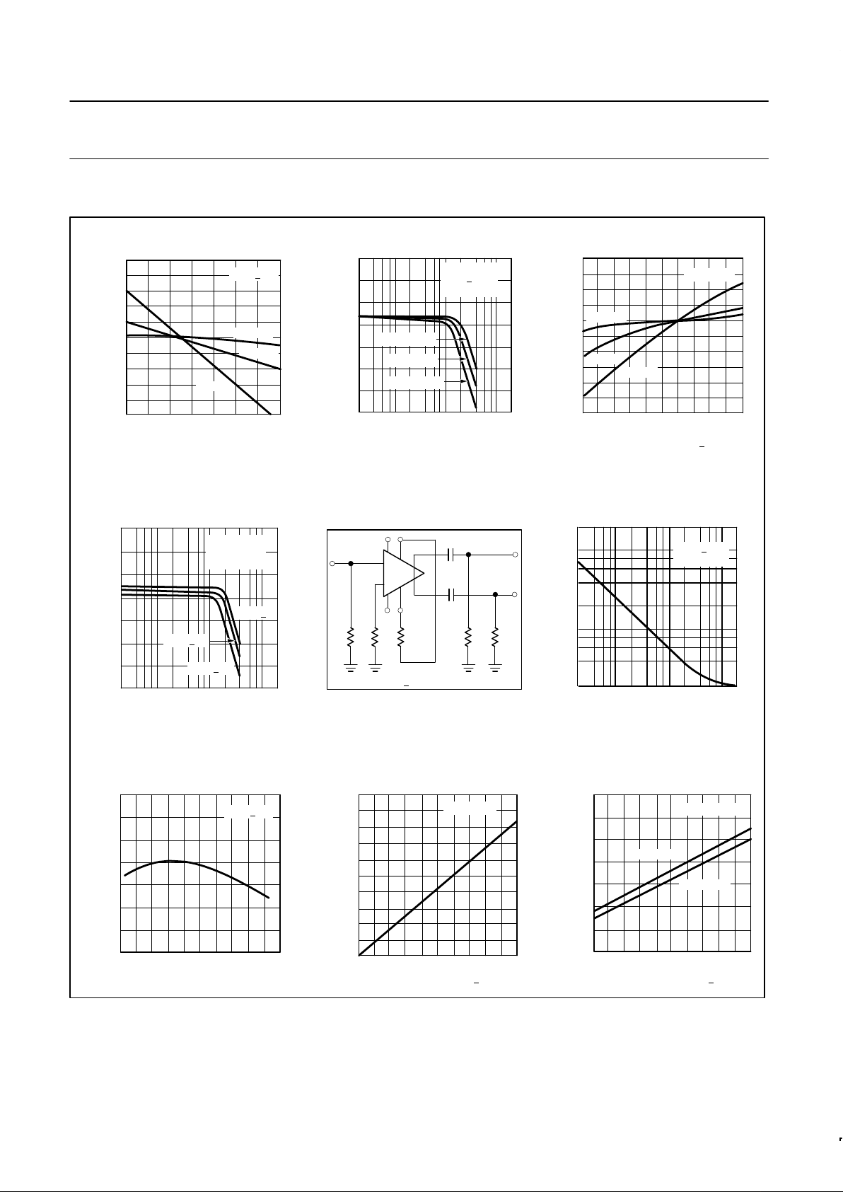
TYPICAL PERFORMANCE CHARACTERISTICS
OVERDRIVE RECOVERY TIME – ns
70
60
50
40
30
20
10
0
0 20 40 60 80 100 120 140 160 180 200
DIFFERENTIAL INPUT VOLTAGE – mV
VS = +6V
T
A
= 25oC
GAIN 2
PHASE SHIFT – DEGREES
Phase Shift as a
Function of Frequency
0
-5
-10
-15
-20
-25
012345678910
FREQUENCY – MHz
GAIN 2
V
S
= +6V
T
A
= 25oC
COMMON-MODE REJECTION RATIO – dB
Common-Mode Rejection Ratio
as a Function of Frequency
100
90
80
70
60
50
40
30
20
10
0
10k 100k 1M 10M 100M
FREQUENCY – Hz
GAIN 2
V
S
= +6V
T
A
= 25oC
OUTPUT VOLTAGE SWING – Vpp
Output Voltage Swing as
a Function of Frequency
7.0
6.0
5.0
4.0
3.0
2.0
1.0
0
1 5 10 50 100 5001000
FREQUENCY – MHz
VS = +6V
T
A
= 25oC
R
L
= 1kΩ
OUTPUT VOLTAGE – V
Pulse Response as a
Function of Supply Voltage
1.6
1.4
1.2
1.0
0.8
0.6
0.4
0.2
0
-0.2
-0.4
-15 -10 -5 0 5 10 15 20 25 30 35
TIME – ns
GAIN 2
T
A
= 25oC
R
L
= 1kΩ
VS = +8V
VS = +3V
VS = +6V
OUTPUT VOLTAGE – V
TA = 70oC
Pulse Response as a
Function of Temperature
1.6
1.4
1.2
1.0
0.8
0.6
0.4
0.2
0
-0.2
-0.4
-15 -10 -5 0 5 10 15 20 25 30 35
TIME – ns
GAIN 2
V
S
= +
6V
RL = 1kΩ
TA = 25oC
TA = 0oC
0
–60
–100
–150
–200
–250
–300
–350
1 5 10 50 100 5001000
GAIN 3
GAIN 2
GAIN 1
VA = +6V
T
A
= 25oC
PHASE SHIFT — DEGREES
FREQUENCY — MHz
VS = +6V
T
A
= 25oC
RL = 1kKΩ
Phase Shift as a
Function of Frequency
Voltage Gain as a
Function of Temperature
FREQUENCY — MHz
SINGLE ENDED VOLTAGE GAIN – dB
60
50
40
30
20
10
0
-10
GAIN 1
GAIN 2
GAIN 3
1 5 10 50 100 5001000
OUTPUT VOLTAGE – V
1.6
1.4
1.2
1.0
0.8
0.6
0.4
0.2
0
-0.2
-0.4
-15 -10 -5 0 5 10 15 20 25 30 35
TIME – ns
VS = +6V
T
A
= 25oC
R
L
= 1k
GAIN 2
GAIN 1
GAIN 3
Pulse Response
Differential Overdrive
Recovery Time
SL00091
Figure 3. Typical Performance Characteristics
Page 6
Philips Semiconductors Product specification
µA733/733CDifferential video amplifier
1992 Apr 15
6
TYPICAL PERFORMANCE CHARACTERISTICS (Continued)
SUPPLY CURRENT – mA
Supply Current as a
Function of Temperature
21
20
19
18
17
16
15
14
-60
-20 20 60 100 140
TEMPERATURE –
o
C
VS = +6V
SINGLE ENDED VOLTAGE GAIN – dB
Gain vs. Frequency as a
Function of Temperature
60
50
40
30
20
10
0
-10
1 5 10 50 100 500 1000
FREQUENCY – MHz
GAIN 2
V
S
= +6V
R
L
= 1kKΩ
TA = 125oC
TA = –55oC
TA = 25oC
SINGLE ENDED VOLTAGE GAIN – dB
Gain vs. Frequency as a
Function of Supply Voltage
60
50
40
30
20
10
0
-10
1 5 10 50 100 500 1000
FREQUENCY – MHz
VS = +8V
VS = +3V
VS = +6V
GAIN 2
T
A
= 25oC
R
L
= 1kKΩ
14
1
12
11
8
7
4
3
Voltage Gain
Adjust Circuit
0.2µF
0.2µF
733
51Ω 51Ω
R
ADJ
1kΩ1kΩ
T
A
= 25oCVS = +6V
(Pin numbers apply to K Package)
SUPPLY CURRENT – mA
28
24
20
16
12
8
34 5 6 7 8
SUPPLY VOLTAGE – +
V
TA = 25oC
OUTPUT VOLTAGE SWING – V OR
OUTPUT SINK CURRENT – mA
Output Voltage and Current
Swing as a Function of
Supply Voltage
7.0
6.0
5.0
4.0
3.0
2.0
1.0
0
3.0 4.0 5.0 6.0 7.0 8.0
SUPPLY VOLTAGE – +
V
TA = 25oC
VOLTAGE
CURRENT
RELATIVE VOLTAGE GAIN
Voltage Gain as a
Function of Temperature
1.10
1.08
1.06
1.04
1.02
1.00
0.98
0.96
0.94
0.92
0.90
0 102030 40506070
TEMPERATURE –
o
C
VS = +
6V
GAIN 2
GAIN 1
GAIN 3
RELATIVE VOLTAGE GAIN
Voltage Gain as a
Function of Supply Voltage
1.4
1.3
1.2
1.1
1.0
0.9
0.8
0.7
0.6
0.5
0.4
345 67 8
SUPPLY VOLTAGE – +
V
TA = 25oC
GAIN 2
GAIN 1
GAIN 3
1000
100
10
10 100 1K 10K
R
ADJ
– Ω
VS = +6V
T
A
= 25oC
DIFFERENTIAL VOLTAGE GAIN – V/V
Voltage Gain as a
Function of RADJ (Figure 3)
Supply Current as a
Function of Supply Voltage
SL00092
Figure 4. Typical Performance Characteristics (cont.)
Page 7
Philips Semiconductors Product specification
µA733/733CDifferential video amplifier
1992 Apr 15
7
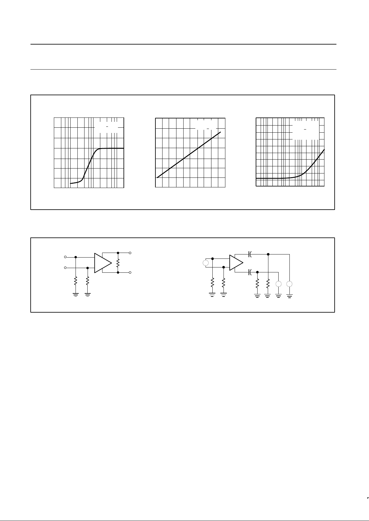
TYPICAL PERFORMANCE CHARACTERISTICS (Continued)
OUTPUT VOLTAGE SWING – Vpp
Output Voltage Swing as a
Function of Load Resistance
7.0
6.0
5.0
4.0
3.0
2.0
1.0
0
10 50 100 500 1K 5K 10K
LOAD RESISTANCE – Ω
VS = +6V
T
A
= 25oC
INPUT RESISTANCE – KΩ
Input Resistance as a
Function of Temperature
70
60
50
40
30
20
10
0
-60 -20 0 20 60 100 140
TEMPERATURE –
o
C
GAIN 2
V
S
= +6V
INPUT NOISE VOLTAGE – Vrmsµ
Input Noise Voltage as a
Function of Source Resistance
100
90
80
70
60
50
40
30
20
10
0
1 10 100 1K 10K
SOURCE RESISTANCE – Ω
GAIN 2
V
S
= +6V
T
A
= 25oC
BW = 10MHz
SL00093
Figure 5. Typical Performance Characteristics (cont.)
TEST CIRCUITS T
A
=25°C, unless otherwise specified.
V
OUT
V
IN
R
L
733
51Ω 51Ω
51Ω 51Ω
e
in
e
outeout
1k 1k
0.2µF
0.2µF
733
SL00094
Figure 6. Test Circuits
Page 8
Philips Semiconductors Product specification
µA733/733CDifferential video amplifier
April 15, 1992
8
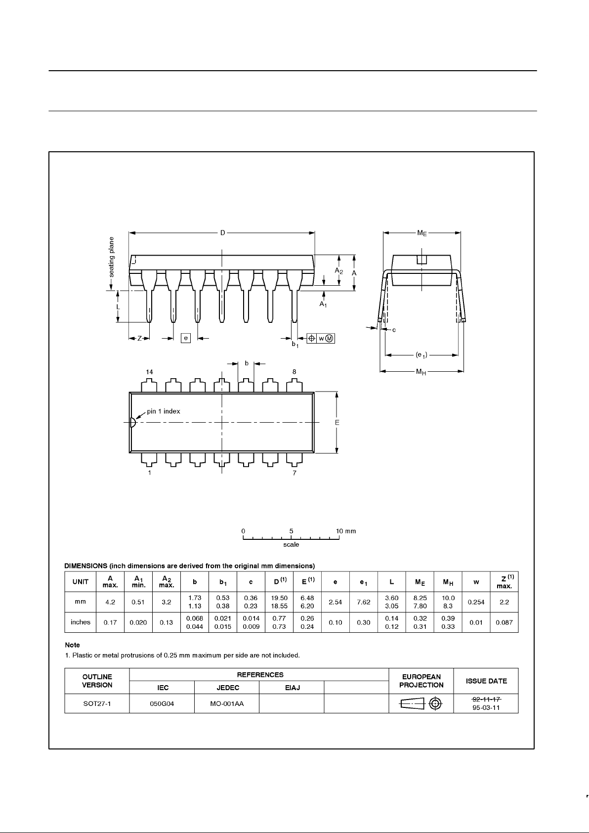
DIP14: plastic dual in-line package; 14 leads (300 mil) SOT27-1
Page 9

Philips Semiconductors Product specification
µA733/733CDifferential video amplifier
April 15, 1992
9
Philips Semiconductors and Philips Electronics North America Corporation reserve the right to make changes, without notice, in the products,
including circuits, standard cells, and/or software, described or contained herein in order to improve design and/or performance. Philips
Semiconductors assumes no responsibility or liability for the use of any of these products, conveys no license or title under any patent, copyright,
or mask work right to these products, and makes no representations or warranties that these products are free from patent, copyright, or mask
work right infringement, unless otherwise specified. Applications that are described herein for any of these products are for illustrative purposes
only. Philips Semiconductors makes no representation or warranty that such applications will be suitable for the specified use without further testing
or modification.
LIFE SUPPORT APPLICA TIONS
Philips Semiconductors and Philips Electronics North America Corporation Products are not designed for use in life support appliances, devices,
or systems where malfunction of a Philips Semiconductors and Philips Electronics North America Corporation Product can reasonably be expected
to result in a personal injury. Philips Semiconductors and Philips Electronics North America Corporation customers using or selling Philips
Semiconductors and Philips Electronics North America Corporation Products for use in such applications do so at their own risk and agree to fully
indemnify Philips Semiconductors and Philips Electronics North America Corporation for any damages resulting from such improper use or sale.
This data sheet contains preliminary data, and supplementary data will be published at a later date. Philips
Semiconductors reserves the right to make changes at any time without notice in order to improve design
and supply the best possible product.
Philips Semiconductors and Philips Electronics North America Corporation
register eligible circuits under the Semiconductor Chip Protection Act.
Copyright Philips Electronics North America Corporation 1992
All rights reserved. Printed in U.S.A.
Philips Semiconductors
811 East Arques Avenue
P.O. Box 3409
Sunnyvale, California 94088–3409
Telephone 800-234-7381
DEFINITIONS
Data Sheet Identification Product Status Definition
Objective Specification
Preliminary Specification
Product Specification
Formative or in Design
Preproduction Product
Full Production
This data sheet contains the design target or goal specifications for product development. Specifications
may change in any manner without notice.
This data sheet contains Final Specifications. Philips Semiconductors reserves the right to make changes
at any time without notice, in order to improve design and supply the best possible product.
 Loading...