


l
Data Manua
November 2006 CS Peripheral
SLLS535D

IMPORTANT NOTICE
Texas Instruments Incorporated and its subsidiaries (TI) reserve the right to make corrections, modifications,
enhancements, improvements, and other changes to its products and services at any time and to discontinue
any product or service without notice. Customers should obtain the latest relevant information before placing
orders and should verify that such information is current and complete. All products are sold subject to TI’s terms
and conditions of sale supplied at the time of order acknowledgment.
TI warrants performance of its hardware products to the specifications applicable at the time of sale in
accordance with TI’s standard warranty. Testing and other quality control techniques are used to the extent TI
deems necessary to support this warranty . Except where mandated by government requirements, testing of all
parameters of each product is not necessarily performed.
TI assumes no liability for applications assistance or customer product design. Customers are responsible for
their products and applications using TI components. To minimize the risks associated with customer products
and applications, customers should provide adequate design and operating safeguards.
TI does not warrant or represent that any license, either express or implied, is granted under any TI patent right,
copyright, mask work right, or other TI intellectual property right relating to any combination, machine, or process
in which TI products or services are used. Information published by TI regarding third-party products or services
does not constitute a license from TI to use such products or services or a warranty or endorsement thereof.
Use of such information may require a license from a third party under the patents or other intellectual property
of the third party, or a license from TI under the patents or other intellectual property of TI.
Reproduction of information in TI data books or data sheets is permissible only if reproduction is without
alteration and is accompanied by all associated warranties, conditions, limitations, and notices. Reproduction
of this information with alteration is an unfair and deceptive business practice. TI is not responsible or liable for
such altered documentation.
Resale of TI products or services with statements different from or beyond the parameters stated by TI for that
product or service voids all express and any implied warranties for the associated TI product or service and
is an unfair and deceptive business practice. TI is not responsible or liable for any such statements.
Following are URLs where you can obtain information on other Texas Instruments products and application
solutions:
Products Applications
Amplifiers amplifier.ti.com Audio www.ti.com/audio
Data Converters dataconverter.ti.com Automotive www.ti.com/automotive
DSP dsp.ti.com Broadband www.ti.com/broadband
Interface interface.ti.com Digital Control www.ti.com/digitalcontrol
Logic logic.ti.com Military www.ti.com/military
Power Mgmt power.ti.com Optical Networking www.ti.com/opticalnetwork
Microcontrollers microcontroller.ti.com Security www.ti.com/security
Low Power Wireless www.ti.com/lpw Telephony www.ti.com/telephony
Video & Imaging www.ti.com/video
Wireless www.ti.com/wireless
Mailing Address: Texas Instruments
Post Office Box 655303 Dallas, Texas 75265
Copyright 2006, Texas Instruments Incorporated

Contents
Contents
Section Page
1 Controller Description 1−1. . . . . . . . . . . . . . . . . . . . . . . . . . . . . . . . . . . . . . . . . . . . . . . . . . . . . . . . . . . . . . . . . . . . . .
1.1 Acronyms and Terms 1−1. . . . . . . . . . . . . . . . . . . . . . . . . . . . . . . . . . . . . . . . . . . . . . . . . . . . . . . . . . . . . . . . . .
2 Main Features 2−1. . . . . . . . . . . . . . . . . . . . . . . . . . . . . . . . . . . . . . . . . . . . . . . . . . . . . . . . . . . . . . . . . . . . . . . . . . . . . .
2.1 Universal Serial Bus (USB) 2−1. . . . . . . . . . . . . . . . . . . . . . . . . . . . . . . . . . . . . . . . . . . . . . . . . . . . . . . . . . . .
2.2 Microcontroller Unit (MCU) 2−1. . . . . . . . . . . . . . . . . . . . . . . . . . . . . . . . . . . . . . . . . . . . . . . . . . . . . . . . . . . . .
2.3 ATA/ATAPI Interface Controller 2−1. . . . . . . . . . . . . . . . . . . . . . . . . . . . . . . . . . . . . . . . . . . . . . . . . . . . . . . . .
2.4 General Feature 2−2. . . . . . . . . . . . . . . . . . . . . . . . . . . . . . . . . . . . . . . . . . . . . . . . . . . . . . . . . . . . . . . . . . . . . .
3 Device Block Diagrams 3−1. . . . . . . . . . . . . . . . . . . . . . . . . . . . . . . . . . . . . . . . . . . . . . . . . . . . . . . . . . . . . . . . . . . . .
4 Device Parameter Information 4−1. . . . . . . . . . . . . . . . . . . . . . . . . . . . . . . . . . . . . . . . . . . . . . . . . . . . . . . . . . . . . . .
4.1 Pin Diagram 4−1. . . . . . . . . . . . . . . . . . . . . . . . . . . . . . . . . . . . . . . . . . . . . . . . . . . . . . . . . . . . . . . . . . . . . . . . .
4.2 Terminal Functions 4−2. . . . . . . . . . . . . . . . . . . . . . . . . . . . . . . . . . . . . . . . . . . . . . . . . . . . . . . . . . . . . . . . . . . .
4.3 Device Operation 4−5. . . . . . . . . . . . . . . . . . . . . . . . . . . . . . . . . . . . . . . . . . . . . . . . . . . . . . . . . . . . . . . . . . . . .
4.3.1 Device Master Reset 4−5. . . . . . . . . . . . . . . . . . . . . . . . . . . . . . . . . . . . . . . . . . . . . . . . . . . . . . . .
4.3.2 Clock Generation 4−5. . . . . . . . . . . . . . . . . . . . . . . . . . . . . . . . . . . . . . . . . . . . . . . . . . . . . . . . . . . .
4.3.3 Device Initialization 4−5. . . . . . . . . . . . . . . . . . . . . . . . . . . . . . . . . . . . . . . . . . . . . . . . . . . . . . . . . .
5 Architecture Overview 5−1. . . . . . . . . . . . . . . . . . . . . . . . . . . . . . . . . . . . . . . . . . . . . . . . . . . . . . . . . . . . . . . . . . . . . .
5.1 Controller Brief Data Flow 5−1. . . . . . . . . . . . . . . . . . . . . . . . . . . . . . . . . . . . . . . . . . . . . . . . . . . . . . . . . . . . . .
5.2 Overview of Major Function Blocks 5−2. . . . . . . . . . . . . . . . . . . . . . . . . . . . . . . . . . . . . . . . . . . . . . . . . . . . . .
5.2.1 USB 2.0 UTMI-Compliant PHY 5−2. . . . . . . . . . . . . . . . . . . . . . . . . . . . . . . . . . . . . . . . . . . . . . . .
5.2.2 USB 2.0 Parallel Interface Engine (PIE) 5−2. . . . . . . . . . . . . . . . . . . . . . . . . . . . . . . . . . . . . . . .
5.2.3 USB Buffer Manager (UBM) 5−3. . . . . . . . . . . . . . . . . . . . . . . . . . . . . . . . . . . . . . . . . . . . . . . . . .
5.2.4 Embedded Microcontroller Unit (MCU) 5−3. . . . . . . . . . . . . . . . . . . . . . . . . . . . . . . . . . . . . . . . .
5.2.5 ATA/ATAPI Interface Controller 5−3. . . . . . . . . . . . . . . . . . . . . . . . . . . . . . . . . . . . . . . . . . . . . . . .
5.2.6 I2C Interface Controller 5−4. . . . . . . . . . . . . . . . . . . . . . . . . . . . . . . . . . . . . . . . . . . . . . . . . . . . . .
5.3 Other Major Features 5−4. . . . . . . . . . . . . . . . . . . . . . . . . . . . . . . . . . . . . . . . . . . . . . . . . . . . . . . . . . . . . . . . .
5.3.1 Unique Power-On Sequencing to the Storage Device 5−4. . . . . . . . . . . . . . . . . . . . . . . . . . . .
5.3.2 Die-ID Based USB Device Serial Number 5−4. . . . . . . . . . . . . . . . . . . . . . . . . . . . . . . . . . . . . . .
6 Microcontroller Unit (MCU) 6−1. . . . . . . . . . . . . . . . . . . . . . . . . . . . . . . . . . . . . . . . . . . . . . . . . . . . . . . . . . . . . . . . . .
6.1 MCU Memory Map 6−1. . . . . . . . . . . . . . . . . . . . . . . . . . . . . . . . . . . . . . . . . . . . . . . . . . . . . . . . . . . . . . . . . . . .
6.2 Internal XDATA Space [E000 → F0F9] 6−3. . . . . . . . . . . . . . . . . . . . . . . . . . . . . . . . . . . . . . . . . . . . . . . . . . .
6.3 MCU Control and Status Registers (in SFR and ESFR Space) 6−8. . . . . . . . . . . . . . . . . . . . . . . . . . . . . .
6.3.1 PCON: Power Control Register (at SFR 87h) 6−9. . . . . . . . . . . . . . . . . . . . . . . . . . . . . . . . . . .
6.3.2 RTKTM: RTK Timer Register (at ESFR F6h) 6−9. . . . . . . . . . . . . . . . . . . . . . . . . . . . . . . . . . . .
6.3.3 WDCSR: Watchdog Timer Control and Status Register (at ESFR FBh) 6−10. . . . . . . . . . . .
6.3.4 MCUCNFG: MCU Configuration Register (at ESFR FCh) 6−10. . . . . . . . . . . . . . . . . . . . . . . .
6.3.5 PWONSUSP: Power-On Reset and Suspend Detection Register (at ESFR FDh) 6−11. . .
7 Interrupts 7−1. . . . . . . . . . . . . . . . . . . . . . . . . . . . . . . . . . . . . . . . . . . . . . . . . . . . . . . . . . . . . . . . . . . . . . . . . . . . . . . . . .
7.1 8051 Interrupt and Status Registers 7−1. . . . . . . . . . . . . . . . . . . . . . . . . . . . . . . . . . . . . . . . . . . . . . . . . . . . .
7.1.1 IE: Interrupt Enable Register (SFR at A8) 7−2. . . . . . . . . . . . . . . . . . . . . . . . . . . . . . . . . . . . . . .
7.1.2 IP: Interrupt Priority Register (SFR at B8) 7−2. . . . . . . . . . . . . . . . . . . . . . . . . . . . . . . . . . . . . . .
7.1.3 IE1: Interrupt Enable Register (SFR at E8) 7−3. . . . . . . . . . . . . . . . . . . . . . . . . . . . . . . . . . . . .
7.1.4 IP1: Interrupt Priority Register (SFR at F8) 7−3. . . . . . . . . . . . . . . . . . . . . . . . . . . . . . . . . . . . . .
7.1.5 TCON: Timer/Counter Control Register (SFR at 88) 7−3. . . . . . . . . . . . . . . . . . . . . . . . . . . . . .
7.2 Additional Interrupt Sources 7−4. . . . . . . . . . . . . . . . . . . . . . . . . . . . . . . . . . . . . . . . . . . . . . . . . . . . . . . . . . . .
7.2.1 VECINT: Vector Interrupt Register (ESFR at F7) 7−4. . . . . . . . . . . . . . . . . . . . . . . . . . . . . . . . .
SLLS535D − November 2006 TUSB6250
iii

Contents
Section Page
8 USB Function and Registers 8−1. . . . . . . . . . . . . . . . . . . . . . . . . . . . . . . . . . . . . . . . . . . . . . . . . . . . . . . . . . . . . . . .
8.1 USBCTL: USB Control Register (XDATA at F006) 8−1. . . . . . . . . . . . . . . . . . . . . . . . . . . . . . . . . . . . . . . . .
8.1.1 USB Enumeration 8−1. . . . . . . . . . . . . . . . . . . . . . . . . . . . . . . . . . . . . . . . . . . . . . . . . . . . . . . . . . .
8.1.2 USB Reset 8−2. . . . . . . . . . . . . . . . . . . . . . . . . . . . . . . . . . . . . . . . . . . . . . . . . . . . . . . . . . . . . . . . .
8.1.3 USB 2.0 Test Mode 8−2. . . . . . . . . . . . . . . . . . . . . . . . . . . . . . . . . . . . . . . . . . . . . . . . . . . . . . . . . .
8.2 USBMSK: USB Interrupt Mask Register (XDATA at F007) 8−3. . . . . . . . . . . . . . . . . . . . . . . . . . . . . . . . . .
8.3 USBSTA: USB Status Register (XDATA at F008) 8−4. . . . . . . . . . . . . . . . . . . . . . . . . . . . . . . . . . . . . . . . .
8.3.1 USB Suspend 8−4. . . . . . . . . . . . . . . . . . . . . . . . . . . . . . . . . . . . . . . . . . . . . . . . . . . . . . . . . . . . . .
8.3.2 WAKCLK Interrupt and Remote Wake-Up 8−5. . . . . . . . . . . . . . . . . . . . . . . . . . . . . . . . . . . . . .
8.4 FUNADR: Function Address Register (XDATA at F009) 8−9. . . . . . . . . . . . . . . . . . . . . . . . . . . . . . . . . . . .
8.5 UTMICFG: UTMI Configuration Status Register (XDATA at F00A) 8−9. . . . . . . . . . . . . . . . . . . . . . . . . . .
8.6 USBFCL: USB Frame Counter Low-Byte Register (XDATA at F00B) 8−10. . . . . . . . . . . . . . . . . . . . . . . .
8.7 USBFCH: USB Frame Counter High-Byte Register (XDATA at F00C) 8−10. . . . . . . . . . . . . . . . . . . . . . .
8.8 USBWKUP: USB Wake-Up Reason Register (XDATA at F00D) 8−10. . . . . . . . . . . . . . . . . . . . . . . . . . . .
8.9 Endpoint-0 Descriptor Registers 8−12. . . . . . . . . . . . . . . . . . . . . . . . . . . . . . . . . . . . . . . . . . . . . . . . . . . . . . .
8.9.1 IEPCNFG_0: Input Endpoint-0 Configuration Register (XDATA at F000) 8−13. . . . . . . . . . .
8.9.2 IEPBCN_0: Input Endpoint-0 Buffer Byte Count Register (XDATA at F001) 8−13. . . . . . . . .
8.9.3 OEPCNFG_0: Output Endpoint-0 Configuration Register (XDATA at F003) 8−14. . . . . . . . .
8.9.4 OEPBCN_0: Output Endpoint-0 Buffer Byte Count Register (XDATA at F004) 8−14. . . . . .
8.10 Endpoint Descriptor Block (EDB-1 to EDB-4) 8−15. . . . . . . . . . . . . . . . . . . . . . . . . . . . . . . . . . . . . . . . . . . .
8.10.1 IEPCNFG_n: Input Endpoint Configuration (n = 1 to 4)
(XDATA at F010, F020, F030, F040) 8−17. . . . . . . . . . . . . . . . . . . . . . . . . . . . . . . . . . . . . . . . . .
8.10.2 IEPBBADRX_n: Input Endpoint X-Buffer Base Address (n = 1 to 4)
(XDATA at F011, F021, F031, F041) 8−17. . . . . . . . . . . . . . . . . . . . . . . . . . . . . . . . . . . . . . . . . .
8.10.3 IEPBCNLX_n: Input Endpoint X-Buffer Byte Count Low Byte (n = 1 to 4)
(XDATA at F012, F022, F032, F042) 8−18. . . . . . . . . . . . . . . . . . . . . . . . . . . . . . . . . . . . . . . . . .
8.10.4 IEPBCNHX_n: Input Endpoint X-Buffer Byte Count High Byte (n = 1 to 4) (XDATA at
F013, F023, F033, F043) 8−18. . . . . . . . . . . . . . . . . . . . . . . . . . . . . . . . . . . . . . . . . . . . . . . . . . . .
8.10.5 IEPSIZXY_n: Input Endpoint X/Y-Buffer Size (n = 1 to 4) (XDATA at F014,
F024, F034, F044) 8−19. . . . . . . . . . . . . . . . . . . . . . . . . . . . . . . . . . . . . . . . . . . . . . . . . . . . . . . . .
8.10.6 IEPBBADRY_n: Input Endpoint Y-Buffer Base Address (n = 1 to 4)
(XDATA at F015, F025, F035, F045) 8−19. . . . . . . . . . . . . . . . . . . . . . . . . . . . . . . . . . . . . . . . . .
8.10.7 IEPBCNLY_n: Input Endpoint Y-Buffer Byte Count Low Byte (n = 1 to 4)
(XDATA at F016, F026, F036, F046) 8−19. . . . . . . . . . . . . . . . . . . . . . . . . . . . . . . . . . . . . . . . . .
8.10.8 IEPBCNHY_n: Input Endpoint Y-Buffer Byte Count High Byte (n = 1 to 4)
(XDATA at F017, F027, F037, F047) 8−20. . . . . . . . . . . . . . . . . . . . . . . . . . . . . . . . . . . . . . . . . .
8.10.9 OEPCNF_n: Output Endpoint Configuration (n = 1 to 4) (XDATA at F018,
F028, F038, F048) 8−20. . . . . . . . . . . . . . . . . . . . . . . . . . . . . . . . . . . . . . . . . . . . . . . . . . . . . . . . .
8.10.10 OEPBBAX_n: Output Endpoint X-Buffer Base Address (n = 1 to 4)
(XDATA at F019, F029, F039, F049) 8−21. . . . . . . . . . . . . . . . . . . . . . . . . . . . . . . . . . . . . . . . . .
8.10.11 OEPBCNLX_n: Output Endpoint X-Buffer Byte Count Low Byte (n = 1 to 4)
(XDATA at F01A, F02A, F03A, F04A) 8−21. . . . . . . . . . . . . . . . . . . . . . . . . . . . . . . . . . . . . . . . .
8.10.12 OEPBCNHX_n: Output Endpoint X-Buffer Byte Count High Byte (n = 1 to 4)
(XDATA at F01B, F02B, F03B, F04B) 8−21. . . . . . . . . . . . . . . . . . . . . . . . . . . . . . . . . . . . . . . . .
8.10.13 OEPSIZXY_n: Output Endpoint X/Y-Buffer Size (n = 1 to 4) (XDATA at F01C,
F02C, F03C, F04C) 8−22. . . . . . . . . . . . . . . . . . . . . . . . . . . . . . . . . . . . . . . . . . . . . . . . . . . . . . . .
8.10.14 OEPBBADRY_n: Output Endpoint Y-Buffer Base Address (n = 1 to 4)
(XDATA at F01D, F02D, F03D, F04D) 8−22. . . . . . . . . . . . . . . . . . . . . . . . . . . . . . . . . . . . . . . .
8.10.15 OEPBCNLY_n: Output Endpoint Y-Buffer Byte Count Low Byte (n = 1 to 4)
(XDATA at F01E, F02E, F03E, F04E) 8−22. . . . . . . . . . . . . . . . . . . . . . . . . . . . . . . . . . . . . . . . .
8.10.16 OEPBCNHY_n: Output Endpoint Y-Buffer Byte Count High Byte (n = 1 to 4)
(XDATA at F01F, F02F, F03F, F04F) 8−23. . . . . . . . . . . . . . . . . . . . . . . . . . . . . . . . . . . . . . . . . .
iv
SLLS535D − November 2006TUSB6250

Contents
Section Page
8.11 Serial Number Registers 8−24. . . . . . . . . . . . . . . . . . . . . . . . . . . . . . . . . . . . . . . . . . . . . . . . . . . . . . . . . . . . . .
8.11.1 SERNUMn: Device Serial Number Register (Byte n, n = 0 to 5)
(XDATA at F080 to F085) 8−24. . . . . . . . . . . . . . . . . . . . . . . . . . . . . . . . . . . . . . . . . . . . . . . . . . .
9 Miscellaneous and GPIO Configuration Registers 9−1. . . . . . . . . . . . . . . . . . . . . . . . . . . . . . . . . . . . . . . . . . . . .
9.1 MODECNFG: Mode Configuration Register (XDATA at F088) 9−2. . . . . . . . . . . . . . . . . . . . . . . . . . . . . . .
9.2 PUPDSLCT_P2: GPIO Pullup and Pulldown Resistor Selection Register for Port 2
(XDATA at F08A) 9−3. . . . . . . . . . . . . . . . . . . . . . . . . . . . . . . . . . . . . . . . . . . . . . . . . . . . . . . . . . . . . . . . . . . . .
9.3 PUPDWDN_P2: GPIO Pullup and Pulldown Resistor Power Down for Port 2
(XDATA at F08B) 9−4. . . . . . . . . . . . . . . . . . . . . . . . . . . . . . . . . . . . . . . . . . . . . . . . . . . . . . . . . . . . . . . . . . . . .
9.4 PUPDSLCT_P3: GPIO Pullup and Pulldown Resistor Selection Register for Port 3
(XDATA at F08C) 9−4. . . . . . . . . . . . . . . . . . . . . . . . . . . . . . . . . . . . . . . . . . . . . . . . . . . . . . . . . . . . . . . . . . . . .
9.5 PUPDPWDN_P3: GPIO Pullup and Pulldown Resistor Power Down Register for Port 3
(XDATA at F08D) 9−5. . . . . . . . . . . . . . . . . . . . . . . . . . . . . . . . . . . . . . . . . . . . . . . . . . . . . . . . . . . . . . . . . . . . .
9.6 PUPDFUNC: Pullup/Pulldown Configuration Register for Functional Pins (XDATA at F08E) 9−6. . . . .
9.7 PUPDSLCT_ATPOUT: Pullup and Pulldown Resistor Selection Register for ATA/ATAPI
Outputs (XDATA at F08F) 9−7. . . . . . . . . . . . . . . . . . . . . . . . . . . . . . . . . . . . . . . . . . . . . . . . . . . . . . . . . . . . . .
9.8 PUPDPWDN_ATPOUT: Pullup and Pulldown Resistors Power Down Register for
ATA/ATAPI Outputs (XDATA at F090 9−8. . . . . . . . . . . . . . . . . . . . . . . . . . . . . . . . . . . . . . . . . . . . . . . . . . . .
2
C Interface Controller 10−1. . . . . . . . . . . . . . . . . . . . . . . . . . . . . . . . . . . . . . . . . . . . . . . . . . . . . . . . . . . . . . . . . . . .
10 I
10.1 I2C Registers 10−2. . . . . . . . . . . . . . . . . . . . . . . . . . . . . . . . . . . . . . . . . . . . . . . . . . . . . . . . . . . . . . . . . . . . . . .
10.1.1 IECSCR: I2C Status and Control Register (XDATA at F0B0) 10−2. . . . . . . . . . . . . . . . . . . . .
10.1.2 I2CADR: I2C Device Address Register (XDATA at F0B1) 10−2. . . . . . . . . . . . . . . . . . . . . . . .
10.1.3 I2CDIN: I2C Data_In Register (XDATA at F0B2) 10−3. . . . . . . . . . . . . . . . . . . . . . . . . . . . . . . .
10.1.4 I2CDOUT: I2C Data_Out Register (XDATA at F0B3) 10−3. . . . . . . . . . . . . . . . . . . . . . . . . . . .
10.2 Random-Read Operation 10−4. . . . . . . . . . . . . . . . . . . . . . . . . . . . . . . . . . . . . . . . . . . . . . . . . . . . . . . . . . . . .
10.3 Current-Address Read Operation 10−4. . . . . . . . . . . . . . . . . . . . . . . . . . . . . . . . . . . . . . . . . . . . . . . . . . . . . .
10.4 Sequential-Read Operation 10−5. . . . . . . . . . . . . . . . . . . . . . . . . . . . . . . . . . . . . . . . . . . . . . . . . . . . . . . . . . .
10.5 Byte-Write Operation 10−6. . . . . . . . . . . . . . . . . . . . . . . . . . . . . . . . . . . . . . . . . . . . . . . . . . . . . . . . . . . . . . . . .
10.6 Page-Write Operation 10−7. . . . . . . . . . . . . . . . . . . . . . . . . . . . . . . . . . . . . . . . . . . . . . . . . . . . . . . . . . . . . . . .
10.7 I2C EEPROM Head Block 10−8. . . . . . . . . . . . . . . . . . . . . . . . . . . . . . . . . . . . . . . . . . . . . . . . . . . . . . . . . . . .
11 ATA/ATAPI Interface Port 11−1. . . . . . . . . . . . . . . . . . . . . . . . . . . . . . . . . . . . . . . . . . . . . . . . . . . . . . . . . . . . . . . . . . .
11.1 TUSB6250 ATA Controller Architecture Overview 11−2. . . . . . . . . . . . . . . . . . . . . . . . . . . . . . . . . . . . . . . .
11.1.1 ATA Controller State Machine 11−2. . . . . . . . . . . . . . . . . . . . . . . . . . . . . . . . . . . . . . . . . . . . . . . .
11.1.2 Sector FIFO Controller 11−2. . . . . . . . . . . . . . . . . . . . . . . . . . . . . . . . . . . . . . . . . . . . . . . . . . . . . .
11.1.3 ATA/ATAPI CSR Registers 11−3. . . . . . . . . . . . . . . . . . . . . . . . . . . . . . . . . . . . . . . . . . . . . . . . . .
11.2 ATA/ATAPI Port Power-On Sequencing and 3-State Control 11−4. . . . . . . . . . . . . . . . . . . . . . . . . . . . . . .
11.3 TUSB6250 ATA/ATAPI Controller Transfer Modes 11−6. . . . . . . . . . . . . . . . . . . . . . . . . . . . . . . . . . . . . . . .
11.4 ATA/ATAPI Group 0 (Task_File) Registers 11−8. . . . . . . . . . . . . . . . . . . . . . . . . . . . . . . . . . . . . . . . . . . . . . .
11.5 ATA/ATAPI Group 1 Registers 11−9. . . . . . . . . . . . . . . . . . . . . . . . . . . . . . . . . . . . . . . . . . . . . . . . . . . . . . . . .
11.5.1 ATPIFCNFG0: ATA/ATAPI Interface Configuration Register 0 (XDATA at F0D0) 11−9. . . .
11.5.2 ATPIFCNFG1: ATA/ATAPI Interface Configuration Register 1 (XDATA at F0D1) 11−11. . .
11.5.3 ATPACSREG0: ATA/ATAPI Access Register 0 (XDATA at F0D2) 11−12. . . . . . . . . . . . . . . .
11.5.4 ATPACSREG1: ATA/ATAPI Access Register 1 (XDATA at F0D3) 11−12. . . . . . . . . . . . . . . .
11.5.5 ATPACSREG2: ATA/ATAPI Access Register 2 (XDATA at F0D4) 11−12. . . . . . . . . . . . . . . .
11.5.6 ATPACSREG3: ATA/ATAPI Access Register 3 (XDATA at F0D5) 11−13. . . . . . . . . . . . . . . .
11.5.7 TRANSBCNT0: USB or ATA/ATAPI Transfer Byte Count Register 0
(XDATA at F0D6) 11−13. . . . . . . . . . . . . . . . . . . . . . . . . . . . . . . . . . . . . . . . . . . . . . . . . . . . . . . . .
11.5.8 TRANSBCNT1: USB or ATA/ATAPI Transfer Byte Count Register 1
(XDATA at F0D7) 11−14. . . . . . . . . . . . . . . . . . . . . . . . . . . . . . . . . . . . . . . . . . . . . . . . . . . . . . . . .
11.5.9 TRANSBCNT2: USB or ATA/ATAPI Transfer Byte Count Register 2
(XDATA at F0D8) 11−14. . . . . . . . . . . . . . . . . . . . . . . . . . . . . . . . . . . . . . . . . . . . . . . . . . . . . . . . .
SLLS535D − November 2006 TUSB6250
v

Contents
Section Page
11.5.10 TRANSBCNT3: USB or ATA/ATAPI Transfer Byte Count Register 3
(XDATA at F0D9) 11−14. . . . . . . . . . . . . . . . . . . . . . . . . . . . . . . . . . . . . . . . . . . . . . . . . . . . . . . . .
11.5.11 CMNDLNGTH: Command Length Register (XDATA at F0DA) 11−15. . . . . . . . . . . . . . . . . . .
11.5.12 PIOSPAS: PIO Transfer Speed (Assertion Time) Register (XDATA at F0DC) 11−15. . . . . .
11.5.13 PIOSPRC: PIO Transfer Speed (Recovery Time) Register (XDATA at F0DD) 11−16. . . . . .
11.5.14 DMASPAS: DMA Transfer Speed (Assertion Time) Register (XDATA at F0DE) 11−16. . . .
11.5.15 DMASPRC: DMA Transfer Speed (Recovery Time) Register (XDATA at F0DF) 11−16. . . .
11.5.16 Data Transfer Mode and Timing Reference Chart 11−17. . . . . . . . . . . . . . . . . . . . . . . . . . . . . .
11.6 ATA/ATAPI Group 2 Registers 11−19. . . . . . . . . . . . . . . . . . . . . . . . . . . . . . . . . . . . . . . . . . . . . . . . . . . . . . . .
11.6.1 MCUBYTE0: MCU Data Byte_0 Register (XDATA at F0E0) 11−20. . . . . . . . . . . . . . . . . . . . .
11.6.2 MCUBYTE1: MCU Data Byte_1 Register (XDATA at F0E1) 11−20. . . . . . . . . . . . . . . . . . . . .
11.6.3 MCUBYTE2: MCU Data Byte_2 Register (XDATA at F0E2) 11−20. . . . . . . . . . . . . . . . . . . . .
11.6.4 MCUBYTE3: MCU Data Byte_3 Register (XDATA at F0E3) 11−20. . . . . . . . . . . . . . . . . . . . .
11.6.5 MCUACSL: MCU Access Address Low-Byte Register (XDATA at F0E4 11−21. . . . . . . . . . .
11.6.6 MCUACSH: MCU Access Address High-Byte Register (XDATA at F0E5) 11−21. . . . . . . . .
11.6.7 ATPINTRPT0: ATA/ATAPI Interrupt Register 0 and ATPINTMSK0: ATA/ATAPI
Interrupt Mask Register 0 (XDATA at F0E6, F0E7) 11−21. . . . . . . . . . . . . . . . . . . . . . . . . . . . .
11.6.8 ATPINTRPT1: ATA/ATAPI Interrupt Register 1 and ATPINTMSK1: ATA/ATAPI
Interrupt Mask Register 1 (XDATA at F0E8, F0E9) 11−22. . . . . . . . . . . . . . . . . . . . . . . . . . . . .
11.6.9 ATPSTATUS: ATA/ATAPI Interface Status Register (XDATA at F0EA) 11−23. . . . . . . . . . . .
11.6.10 SECWRPTL: Sector FIFO Write Pointer Low-Byte Register (XDATA at F0EB) 11−24. . . . .
11.6.11 SECWRPTH: Sector FIFO Write Pointer High-Byte Register (XDATA at F0EC) 11−25. . . .
11.6.12 WRPTBKUPL: Sector FIFO Write Pointer Backup Low-Byte Register
(XDATA at F0ED) 11−25. . . . . . . . . . . . . . . . . . . . . . . . . . . . . . . . . . . . . . . . . . . . . . . . . . . . . . . . .
11.6.13 WRPTBKUPH: Sector FIFO Write Pointer Backup High-Byte Register
(XDATA at F0EE) 11−25. . . . . . . . . . . . . . . . . . . . . . . . . . . . . . . . . . . . . . . . . . . . . . . . . . . . . . . . .
11.6.14 SECRDPTL: Sector FIFO Read Pointer Low-Byte Register (XDATA at F0EF 11−25. . . . . .
11.6.15 SECRDPTH: Sector FIFO Read Pointer High-Byte Register (XDATA at F0F0 11−26. . . . .
11.6.16 RDPTBKUPL: Sector FIFO Read Pointer Backup Low-Byte Register
(XDATA at F0F1 11−26. . . . . . . . . . . . . . . . . . . . . . . . . . . . . . . . . . . . . . . . . . . . . . . . . . . . . . . . . .
11.6.17 RDPTBKUPH: Sector FIFO Read Pointer Backup High-Byte Register
(XDATA at F0F2 11−26. . . . . . . . . . . . . . . . . . . . . . . . . . . . . . . . . . . . . . . . . . . . . . . . . . . . . . . . . .
11.6.18 ULRCVEXCNT: Ultrareceive Extra Word Count Register (XDATA at F0F9) 11−27. . . . . . . .
12 Electrical Specifications 12−1. . . . . . . . . . . . . . . . . . . . . . . . . . . . . . . . . . . . . . . . . . . . . . . . . . . . . . . . . . . . . . . . . . .
12.1 Absolute Maximum Ratings 12−1. . . . . . . . . . . . . . . . . . . . . . . . . . . . . . . . . . . . . . . . . . . . . . . . . . . . . . . . . . .
12.2 Recommended Operating Conditions 12−1. . . . . . . . . . . . . . . . . . . . . . . . . . . . . . . . . . . . . . . . . . . . . . . . . . .
12.3 Electrical Characteristics for the Digital Core, T
= 25°C, VCC = 3.3 V ±5%, VSS = 0 V 12−2. . . . . . .
A
12.4 Controller Input Supply Current, TA = 25°C, VCC = 3.3 V ±5%, VSS = 0 V 12−2. . . . . . . . . . . . . . . . . . .
12.5 Timing for 5-V Failsafe TTL Compatible LVCMOS I/O Buffer Used in the TUSB6250
ATA/ATAPI Interface 12−2. . . . . . . . . . . . . . . . . . . . . . . . . . . . . . . . . . . . . . . . . . . . . . . . . . . . . . . . . . . . . . . . .
12.6 Electrical Characteristics for the Integrated USB 2.0 Transceiver, TA = 25°C,
VCC = 3.3 V ±5%, VSS = 0 V 12−3. . . . . . . . . . . . . . . . . . . . . . . . . . . . . . . . . . . . . . . . . . . . . . . . . . . . . . . . . .
13 Application Information 13−1. . . . . . . . . . . . . . . . . . . . . . . . . . . . . . . . . . . . . . . . . . . . . . . . . . . . . . . . . . . . . . . . . . . .
13.1 Crystal Selection and Reference Circuitry 13−1. . . . . . . . . . . . . . . . . . . . . . . . . . . . . . . . . . . . . . . . . . . . . . .
13.2 Reset Timing Reference 13−2. . . . . . . . . . . . . . . . . . . . . . . . . . . . . . . . . . . . . . . . . . . . . . . . . . . . . . . . . . . . . .
13.3 General ATA/ATAPI Device Application Information 13−3. . . . . . . . . . . . . . . . . . . . . . . . . . . . . . . . . . . . . . .
13.3.1 ATA/ATAPI Connector Pin Diagram 13−3. . . . . . . . . . . . . . . . . . . . . . . . . . . . . . . . . . . . . . . . . . .
13.3.2 Special Note About Shaded Signals 13−3. . . . . . . . . . . . . . . . . . . . . . . . . . . . . . . . . . . . . . . . . .
13.3.3 Special Note About Pullup and Pulldown Resistors for ATA/ATAPI Signals 13−5. . . . . . . . .
13.3.4 Series Termination Required for Ultra DMA Operation 13−5. . . . . . . . . . . . . . . . . . . . . . . . . . .
vi
SLLS535D − November 2006TUSB6250

Contents
Section Page
13.4 Compact Flash Storage Card Reader Application 13−6. . . . . . . . . . . . . . . . . . . . . . . . . . . . . . . . . . . . . . . .
13.4.1 Brief Introduction 13−6. . . . . . . . . . . . . . . . . . . . . . . . . . . . . . . . . . . . . . . . . . . . . . . . . . . . . . . . . . .
13.4.2 Pin Assignment and Mapping 13−7. . . . . . . . . . . . . . . . . . . . . . . . . . . . . . . . . . . . . . . . . . . . . . . .
13.4.3 Power-Up Sequence 13−9. . . . . . . . . . . . . . . . . . . . . . . . . . . . . . . . . . . . . . . . . . . . . . . . . . . . . . . .
SLLS535D − November 2006 TUSB6250
vii

List of Illustrations
List of Illustrations
Figure Title Page
3−1 TUSB6250 Block Diagram 3−1. . . . . . . . . . . . . . . . . . . . . . . . . . . . . . . . . . . . . . . . . . . . . . . . . . . . . . . . . . . . . . . . .
3−2 USB 20 PEI (Parallel Interface Engine) Block Diagram 3−2. . . . . . . . . . . . . . . . . . . . . . . . . . . . . . . . . . . . . . . .
4−1 Controller 80-Pin TQFP Pin Diagram 4−1. . . . . . . . . . . . . . . . . . . . . . . . . . . . . . . . . . . . . . . . . . . . . . . . . . . . . . . .
5−1 TUSB6250 Typical Application Diagram 5−1. . . . . . . . . . . . . . . . . . . . . . . . . . . . . . . . . . . . . . . . . . . . . . . . . . . . .
6−1 MCU Memory Map 6−2. . . . . . . . . . . . . . . . . . . . . . . . . . . . . . . . . . . . . . . . . . . . . . . . . . . . . . . . . . . . . . . . . . . . . . .
6−2 IDATA Space Memory Configuration 6−12. . . . . . . . . . . . . . . . . . . . . . . . . . . . . . . . . . . . . . . . . . . . . . . . . . . . . . .
8−1 WAKCLK Interrupt and Wake-Up Status Change Illustration Logical Diagram 8−7. . . . . . . . . . . . . . . . . . . . .
8−2 IN-Endpoint Index Generation 8−16. . . . . . . . . . . . . . . . . . . . . . . . . . . . . . . . . . . . . . . . . . . . . . . . . . . . . . . . . . . . .
8−3 OUT-Endpoint Index Generation 8−16. . . . . . . . . . . . . . . . . . . . . . . . . . . . . . . . . . . . . . . . . . . . . . . . . . . . . . . . . .
8−4 16-Bit EDB Data Buffer Address Generation From the Value of Buffer Base Address 8−16. . . . . . . . . . . . .
11−1 ATA/ATAPI-Port Data Flow Diagram 11−1. . . . . . . . . . . . . . . . . . . . . . . . . . . . . . . . . . . . . . . . . . . . . . . . . . . . . . .
11−2 TUSB6250 ATA/ATAPI Controller Block Diagram 11−2. . . . . . . . . . . . . . . . . . . . . . . . . . . . . . . . . . . . . . . . . . . .
11−3 ATA/ATAPI Bus Powering and Reset Sequence 11−4. . . . . . . . . . . . . . . . . . . . . . . . . . . . . . . . . . . . . . . . . . . . .
13−1 Controller Reference Reset Timing Diagram 13−2. . . . . . . . . . . . . . . . . . . . . . . . . . . . . . . . . . . . . . . . . . . . . . . .
List of Tables
Table Title Page
4−1 Controller Terminal Description (80-Pin TQFP) 4−2. . . . . . . . . . . . . . . . . . . . . . . . . . . . . . . . . . . . . . . . . . . . . . .
6−1 XDATA Space Map [E000 → F0F9] 6−4. . . . . . . . . . . . . . . . . . . . . . . . . . . . . . . . . . . . . . . . . . . . . . . . . . . . . . . .
6−2 Memory Mapped Registers Summary (XDATA Range: F000 → F0F9) 6−3. . . . . . . . . . . . . . . . . . . . . . . . . .
6−3 SFR Map [IDATA: 80 FF] (Shaded Area Indicates ESFRs) 6−8. . . . . . . . . . . . . . . . . . . . . . . . . . . . . . . . . . . .
7−1 8051 Standard/Extended Interrupt Location Map for Application Firmware 7−1. . . . . . . . . . . . . . . . . . . . . . .
7−2 Vector Interrupt Values 7−4. . . . . . . . . . . . . . . . . . . . . . . . . . . . . . . . . . . . . . . . . . . . . . . . . . . . . . . . . . . . . . . . . . .
8−1 Register Setting for the WAKCLK Interrupt and Remote Wake-Up 8−8. . . . . . . . . . . . . . . . . . . . . . . . . . . . . .
8−2 Input/Output EDB-0 Registers 8−13. . . . . . . . . . . . . . . . . . . . . . . . . . . . . . . . . . . . . . . . . . . . . . . . . . . . . . . . . . . .
8−3 Input/Output EDB-0 Buffer Location as Defined by BZ[1:0] 8−13. . . . . . . . . . . . . . . . . . . . . . . . . . . . . . . . . . .
8−4 EDB0 Buffer Locations (in SPRAM) 8−15. . . . . . . . . . . . . . . . . . . . . . . . . . . . . . . . . . . . . . . . . . . . . . . . . . . . . . .
8−5 EDB Entries in MMR (n = 1 to 4) 8−16. . . . . . . . . . . . . . . . . . . . . . . . . . . . . . . . . . . . . . . . . . . . . . . . . . . . . . . . . .
9−1 Controller MCU GPIO Port Mapping 9−1. . . . . . . . . . . . . . . . . . . . . . . . . . . . . . . . . . . . . . . . . . . . . . . . . . . . . . . .
10−1 I2C EEPROM Signature in Descriptor Block 10−8. . . . . . . . . . . . . . . . . . . . . . . . . . . . . . . . . . . . . . . . . . . . . . . .
11−1 Task_File Registers (Group 0) 11−8. . . . . . . . . . . . . . . . . . . . . . . . . . . . . . . . . . . . . . . . . . . . . . . . . . . . . . . . . . . .
11−2 Group 1 Registers 11−10. . . . . . . . . . . . . . . . . . . . . . . . . . . . . . . . . . . . . . . . . . . . . . . . . . . . . . . . . . . . . . . . . . . . .
11−3 ATA and ATAPI Command and Control Block Registers 11−14. . . . . . . . . . . . . . . . . . . . . . . . . . . . . . . . . . . . .
11−4 PIO Mode and Timing Correlation Chart 11−18. . . . . . . . . . . . . . . . . . . . . . . . . . . . . . . . . . . . . . . . . . . . . . . . . .
11−5 Multiword DMA Mode and Timing Correlation Chart 11−19. . . . . . . . . . . . . . . . . . . . . . . . . . . . . . . . . . . . . . . .
11−6 Ultra DMA Mode and Timing Correlation Chart (applies to UDMA Write only) 11−19. . . . . . . . . . . . . . . . . .
11−7 Group 2 Registers 11−20. . . . . . . . . . . . . . . . . . . . . . . . . . . . . . . . . . . . . . . . . . . . . . . . . . . . . . . . . . . . . . . . . . . . .
13−1 ATA/ATAPI Connector Pin Summary 13−3. . . . . . . . . . . . . . . . . . . . . . . . . . . . . . . . . . . . . . . . . . . . . . . . . . . . . .
13−2 Compact Flash Power Consumption (Reference Only) 13−6. . . . . . . . . . . . . . . . . . . . . . . . . . . . . . . . . . . . . . .
13−3 Compact Flash Card System Performance (Reference Only) 13−7. . . . . . . . . . . . . . . . . . . . . . . . . . . . . . . . .
13−4 TUSB6250 Based Compact Flash Storage Card Reader Pin Assignment and Mapping 13−8. . . . . . . . . . .
viii
SLLS535D − November 2006TUSB6250

Controller Description
1 Controller Description
The TUSB6250 is a USB 2.0 HS-capable function controller with an integrated UTMI compliant PHY. The
TUSB6250 is intended as a USB 2.0 to AT A/ATAPI bridge for storage devices using a standard ATA or AT API
interface.
The TUSB6250 is designed to use both the fast performance of the state machine and the programmability
and flexibility of the embedded microcontroller and firmware. With the elaborative balance between the
microcontroller unit (MCU) and the state machine, in addition to its embedded fast MCU (up to 30 MIPS), eight
configurable endpoints, up to 40K bytes of configurable code, and data buffer SRAM, the TUSB6250 provides
a bridge solution to meet both the performance and flexibility requirement of the next-generation external
storage devices. With a low-power-consumption USB 2.0 integrated PHY, the TUSB6250 also enables the
true USB 2.0 high-speed bus-powered application.
1.1 Acronyms and Terms
This section lists and defines some terms and abbreviations used throughout this data manual.
R/O Read-only. Implies a certain register bit is read-only.
W/O Write-only. Implies a certain register bit is write-only . The read operation to this bit normally returns
a zero value.
R/W Read/write. Implies a certain register bit can be accessed with both write and read operations.
R/C Read/set-clear. Implies a certain register bit can be read and cleared to its reset default value by
the MCU writing a certain value to it. The write-to-clear value may vary and depends on the
condition defined in a particular register.
W/C Write/clear. Implies a register bit can be written to perform certain clear functions defined in a
particular register. The bit value being written to remains active for one clock cycle. It is cleared
thereafter automatically. The read operation to this bit always returns a zero value.
MCU Microcontroller unit. In this data manual, MCU refers to the microcontroller embedded in the
TUSB6250.
EDB Endpoint descriptor block. This is a set of registers used to define the characteristics of an endpoint
of a USB device.
UBM USB buffer manager. This is a major functional block of the TUSB6250.
SPRAM Single-port RAM
Little-endian For data with multiple bytes, little-endian means that the byte order is organized such that byte 0
is the least significant byte. The bit order within each individual byte is always the same regardless
of which endianness is used; that is, bit 7 is always the most-significant bit.
Big-endian For data with multiple bytes, big-endian means that the byte order is organized such that byte 0
is the most significant byte. The bit order within each individual byte is always the same regardless
of which endianness is used; that is, bit 7 is always the most-significant bit.
SLLS535D − November 2006 TUSB6250
1−1

Controller Description
1−2
SLLS535D − November 2006TUSB6250

2 Main Features
2.1 Universal Serial Bus (USB)
• Fully compliant with USB 2.0 specification: TID #40390418
• Integrated USB 2.0 UTMI compliant transceiver (PHY)
• Supports USB high speed (HS, 480 Mbits/sec) and full speed (FS, 12 Mbits/sec)
• Supports USB suspend/resume and remote wake-up operation
• Supports USB device-unique serial number by using on-chip unique die ID
• Supports eight configurable endpoints (four input and four output) with a user-programmable buffer size,
in addition to the default control endpoint (endpoint 0):
− Each endpoint can be configured for interrupt and bulk (double-buffered) transfers.
− All endpoints share the 4K-byte data buffer implemented in the SPRAM (single-port SRAM).
2.2 Microcontroller Unit (MCU)
• Integrated 60-MHz 8051 microcontroller with two clocks per cycle (up to 30 MIPS)
• Application code is loadable from either the USB host or the external EEPROM (via the I
• 8K bytes of ROM for the boot loader
• 1152 bytes of RAM with multiple bank selectable capability for the internal data buffer (IDATA space)
• 40K bytes of RAM, configurable for either code or data space, which provides flexibility to the end product
application:
− 32K-byte code RAM with 8K-byte sector buffer data space
− 16K-byte code RAM with 24K-byte sector buffer data space
− 8K-byte code RAM with 32K-byte sector buffer data space
• Master I
transfer speed.
• Up to 13 GPIOs and three general-purpose open-drain outputs can be used for end-product-specific
functions.
2
C interface controller for external device accesses capable of 100 Kbits/sec or 400 Kbits/sec
Main Features
2
C interface)
2.3 ATA/ATAPI Interface Controller
• Supports USB mass storage device class specification bulk-only transfer protocol
• Glueless interface to ATA and ATAPI drives with full ATA and ATAPI protocol support
• High-performance DMA engine supports all PIO, multiword DMA, and UDMA transfer modes up to UDMA
mode 4 (UDMA-66 or ATA-66).
• Correctly handles all 13 cases in bulk-only transfer protocol under all supported transfer modes.
• Fully programmable ATA/ATAPI interface access timing
• Provides multiple flexible transfer options to achieve both high-speed transfer by the state machine and
high flexibility with MCU involvement:
− Fully manual transfer (both command and data) by the MCU
− Semi-automatic transfer with command transfer by the MCU and data transfer by the state machine
− High-performance fully automatic data transfer mainly by the state machine with few MCU
involvements
• Supports mass-storage devices compatible with the ATA/ATAPI-5 specification:
− Hard-disk drive
− DVD/CD-ROM
SLLS535D − November 2006 TUSB6250
2−1

Main Features
− CD-R/W, DVD-R/W
− Compact flash
− PCMCIA type II card or hard drive
− MO drive
• Dual-drive support
− Capable of supporting one master and one slave drive in any combination of ATA and ATAPI.
• Provides easy control to put the ATA/ATAPI bus into a high-impedance state through one register bit
setting.
• 5-V failsafe I/Os for the ATA/ATAPI interface
2.4 General Features
• Operates on a 24-MHz external crystal with on-chip APLL
• Low-power mode (compliant with bus power requirement of <500 µA)
• 3.3-V operation with 1.8-V core operating voltage provided by an on-chip 1.8-V voltage regulator
• Available in an 80-pin TQFP package
2−2
SLLS535D − November 2006TUSB6250
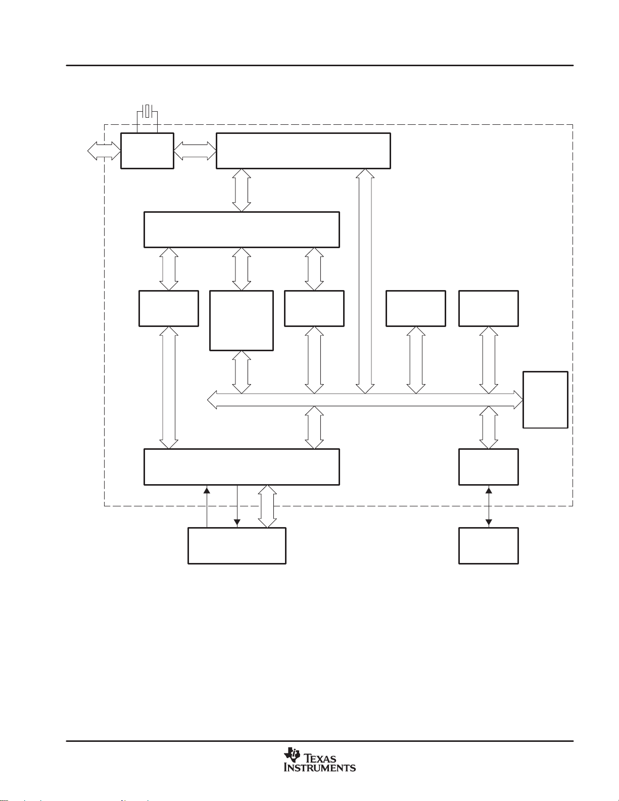
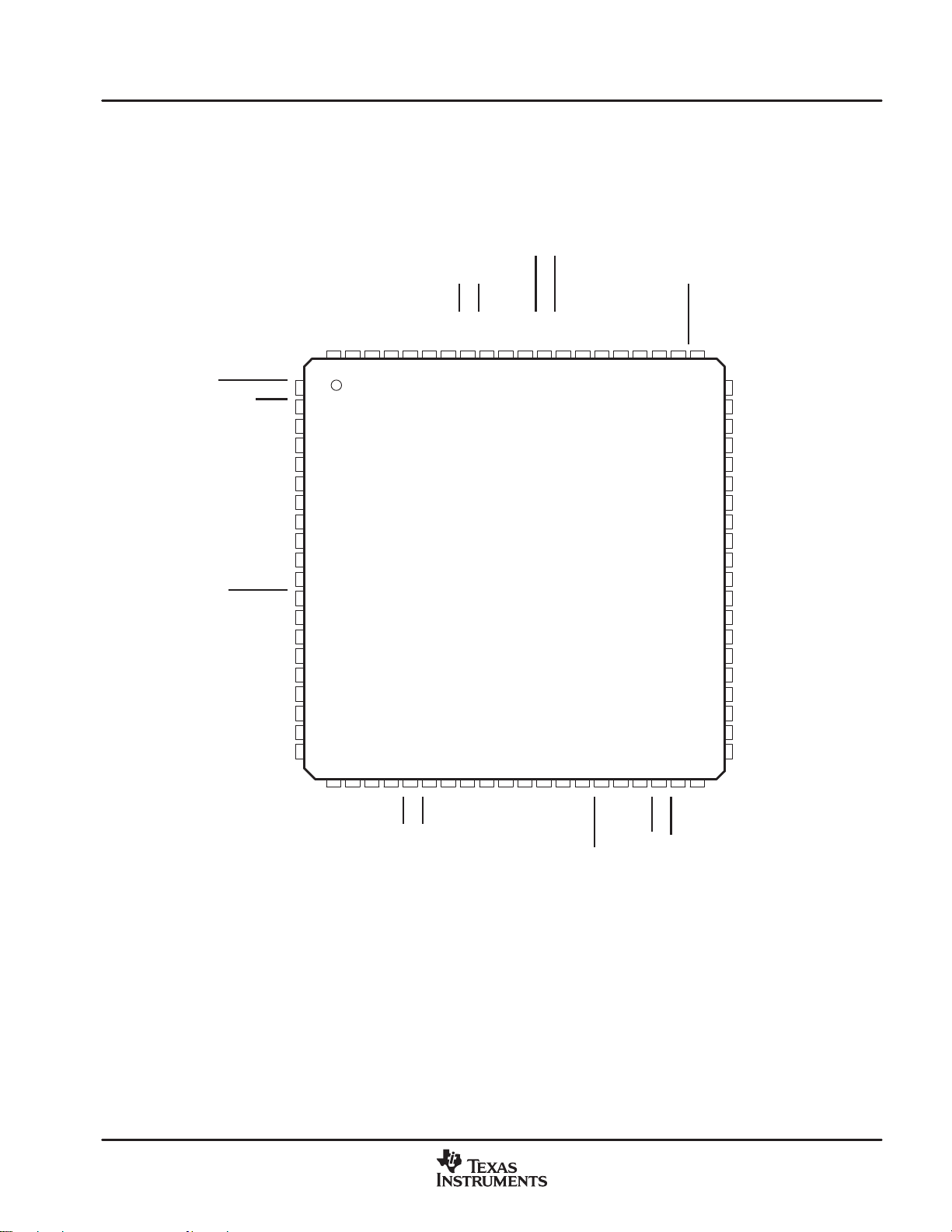
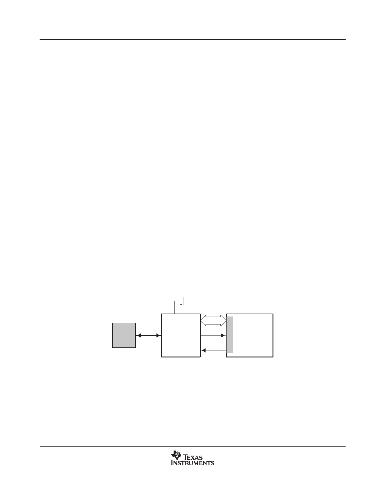
3 Device Block Diagram
24 MHz
Device Block Diagram
USB
Host
USB 2.0
UTMI
8K Byte
(2K × 32)
Data RAM
(See Figure 3−2)
UBM
(USB Buffer Manager)
24K Byte
(6K × 32)
Configurable
RAM for
Code or Data
USB 2.0 PIE
4K Byte
(1K × 32)
SPRAM
8K × 8
Code
RAM
8K × 8
ROM
8051
(60 MHz)
ATA/ATAPI Interface Controller
Standard IDE Devices
Figure 3−1. TUSB6250 Block Diagram
I2C
Controller
I2C
EEPROM
SLLS535D − November 2006 TUSB6250
3−1
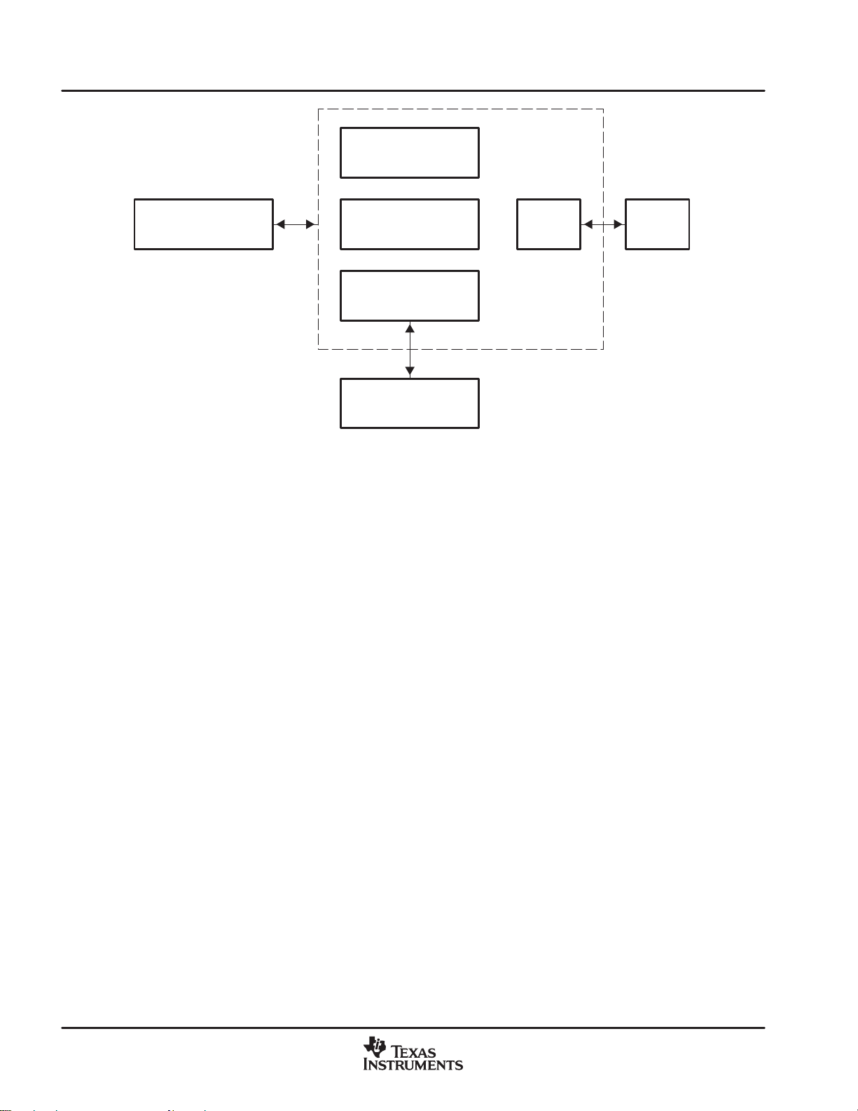
Device Block Diagram
Frame Timer
UTMI-Compliant
Phy
Bus Monitor USB Reg. MCU
Transaction Handler
UBM
(USB Buffer Manager)
Figure 3−2. USB 2.0 PIE (Parallel Interface Engine) Block Diagram
3−2
SLLS535D − November 2006TUSB6250
4 Device Parameter Information
4.1 Pin Diagram
SUSPEND
P3.0/SIN
P3.1/SOUT
DVDD
DVDD18
DGND
TQFP PACKAGE
(TOP VIEW)
P2.0
P3.2/CD1
P3.3/CD2
P3.4
P3.5
P2.1/PWR100
P2.2/PWR500
P2.3
DGND
P2.4
P2.5
Device Parameter Information
DVDD
P2.6
RST_ATA
DVREGEN
RSTI
P2.7
VBUS
RPU
AVDD
AGND
PLLVDD18
UDVDD18
AGND
R1
VREGEN
AVDD
DP
DM
AGND
XTAL2
XTAL1
TSTMODE1
TSTMODE2
79 78 77 76 7580 74 72 71 7073
1
2
3
4
5
6
7
8
9
10
11
12
13
14
15
16
17
18
19
20
22 23
24
SCL
SDA
DVDD
25 26 27 28
CS1
CS0
P3.7
29
DA2
DGND
69 682167 66 65 64
30 31 32 33
DA0
DA1
P3.6
34 35 36 37 38 39 40
DVDD
INTRQ
IORDY
DVDD18
DMACK
63 62 61
DIOR
DGND
60
59
58
57
56
55
54
53
52
51
50
49
48
47
46
45
44
43
42
41
DIOW
DMARQ
DD7
DD8
DD6
DD9
DGND
DD5
DD10
DVDD
DD4
DD11
DD3
DD12
DGND
DD2
DD13
DVDD
DD1
DD14
DD0
DD15
Figure 4−1. Controller 80-Pin TQFP Pin Diagram
SLLS535D − November 2006 TUSB6250
4−1
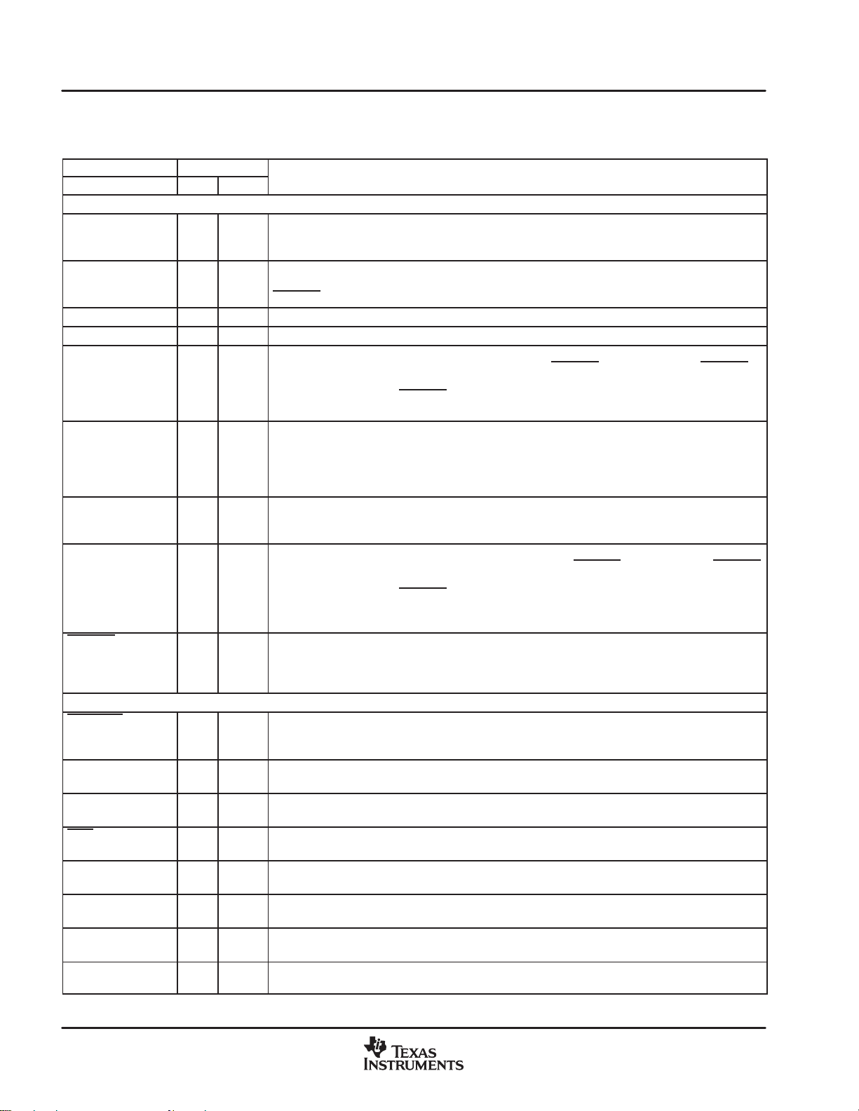
Device Parameter Information
DESCRIPTION
4.2 Terminal Functions
Table 4−1. Controller Terminal Description (80-Pin TQFP)
TERMINAL I/O
NAME NO. TYPE NOTES
INTEGRATED USB 2.0 UTMI-COMPLIANT PHY
AGND 7, 10,16GND Analog ground. All ground terminals should be connected together externally through a
AVDD 6, 13 PWR 3.3-V supply voltage for the integrated USB 2.0 UTMI-compliant PHY’s internal analog circuitry. This
DM 15 I/O USB differential data minus
DP 14 I/O USB differential data plus
PLLVDD18 8 PWR 1.8-V supply for the internal PLL circuitry of the integrated USB 2.0 UTMI-compliant PHY. An internal
R1 11 I/O External reference resistor. An internally generated band-gap voltage is placed on this resistor. The
RPU 5 I/O Pullup resistor connection. This terminal is used to attach and detach the full-speed indicator resistor
UDVDD18 9 PWR 1.92-V supply for the internal digital circuitry of the integrated USB 2.0 UTMI-compliant PHY. An
VREGEN 12 I Voltage regulator enable (active-low). Two internal 3.3-V to 1.8-V voltage regulators supply the digital
CONTROLLER GENERAL
DVREGEN 1 I (4) This active-low terminal is used to enable the 3.3-V to 1.8-V voltage regulator in the TUSB6250’s
P3.0/SIN 79 I/O (1)(6)
P3.1/SOUT 78 I/O (1)(6)
RSTI 2 I (4) The TUSB6250 master reset signal. This active-low terminal is the master reset signal for the
SCL 21 O (7)(8) Master I2C controller: clock signal for external I2C serial EEPROM. The internal 100-µA pullup resistor
SDA 22 I/O (4)(7)
TSTMODE1
TSTMODE21920
VBUS 4 I (5)(10) This terminal monitors the status of the USB upstream VBUS. It has the internal pulldown resistor
I (4)(8) These terminals are used for factory test of the TUSB6250. During normal operation, these terminals
low-impedance path. All bypass capacitors to PLLVDD18, UDVDD18, and AVDD should connect to
ground through a low-impedance path.
supply is also regulated internally down to 1.8 V for use by the PHY’s internal digital circuitry when
VREGEN is asserted. Bypass capacitors to ground are required on these terminals.
voltage regulator generates this supply when terminal VREGEN
de-asserted, 1.8 V must be supplied externally. Bypass capacitance is required on this terminal
regardless of the state of VREGEN. It is recommended that the capacitance on this terminal not be
less then 1 µF.
current through the resistor is mirrored internally to generate the current and voltage used by the
internal analog circuitry. This pin has nominally 1.21 V dc. An external 5.9-kΩ ±1% resistor must be
placed between this terminal and ground. It is recommended that the resistor be placed as close as
possible to this terminal with a minimal trace length to ground.
electrically to/from the DP signal line. An external 1.5-kΩ ±5% resistor must be placed between RPU
and AVDD.
internal voltage regulator generates this supply when terminal VREGEN
is de-asserted, 1.92 V must be supplied externally. Bypass capacitance is required on this terminal
regardless of the state of VREGEN
less then 1 µF. Do not connect the UDVDD18 terminal to the PLLVDD18 or DVDD18 terminal, because
their voltages differ.
and PLL circuitry when this terminal is asserted. When this terminal is de-asserted, the voltage
regulators are disabled and 1.8 V must be supplied externally. TI recommends that this terminal be
tied to ground during normal operation.
digital core. When this terminal is de-asserted, the voltage regulator is disabled and 1.8 V must be
supplied externally. TI recommends that this terminal be tied to ground during normal operation.
This dual-function terminal can be used as either GPIO or the serial data input of the integrated 8051
(8)
microcontroller serial port. The power-up default is to have its internal pullup activated.
This dual-function terminal can be used as either GPIO or the serial data output of the integrated 8051
(8)
microcontroller serial port. The power-up default is to have its internal pullup activated.
TUSB6250. See Section 13.2, Reset Timing Reference, for detailed reset timing information.
on this terminal is always enabled.
Master I2C controller: data signal for external I2C serial EEPROM. The internal 100-µA pullup resistor
(8)
on this terminal is always enabled.
must be left open.
enabled as the power-on reset default.
. It is recommended that the capacitance on this terminal not be
is asserted. When VREGEN is
is asserted. When VREGEN
4−2
SLLS535D − November 2006TUSB6250
Device Parameter Information
DESCRIPTION
Table 4−1. Controller Terminal Description (80-Pin TQFP) (Continued)
TERMINAL I/O
NAME NO. TYPE NOTES
XTAL2 17 O (12) 24-MHz crystal output. This terminal has a 1.8-V LVCMOS output buffer.
XTAL1 18 I (11) 24-MHz crystal input. This terminal has a 1.8-V LVCMOS input buffer.
CONTROLLER POWER/GROUND
DGND 27,37,48,
56,66,75
DVDD 23,33,45,
53,63,77
DVDD18 32, 76 PWR 1.8-V power supply for the internal digital circuitry of the TUSB6250. An internal voltage
SUSPEND 80 O (1) Suspend status indication. This terminal is low during normal operation and active high during
ATA/ATAPI INTERFACE
CS1 25 O (2)(9) ATA/ATAPI: Drive chip select-1. Used to select the control block registers defined by the
CS0 26 O (2)(9) ATA/ATAPI: Drive chip select-0. Used to select the command block registers defined by the
DA [2:0] 28, 31,
29
DD [15:0] 41,43,46,
49,51,54,
57,59,60,
58,55,52,
50,47,44,
42
DMACK 35 O (2)(9) ATA/ATAPI: DMA acknowledge. This terminal should be connected to the corresponding pin of
DMARQ 40 I (5)(10) ATA/ATAPI: DMA request. This 5-V fail-safe terminal has an internal controllable pulldown
DIOR 38 O (2)(9) ATA/A TAPI: Read strobe signal. This terminal should be connected to the corresponding pin of
DIOW 39 O (2)(9) ATA/ATAPI: W rite strobe signal. This terminal should be connected to the corresponding pin of
INTRQ 34 I (5)(9) ATA/ATAPI: Interrupt request. The AT A device asserts this signal when it has a pending interrupt.
IORDY 36 I (5)(9) ATA/ATAPI: Channel ready. This 5-V fail-safe terminal has internal configurable pullup and
P3.6 30 I/O (2)(5)
GND Digital circuit ground terminals. Each ground terminal should be directly connected through a
PWR 3.3-V power-supply terminals for the internal I/O circuitry . Decoupling and filtering capacitors are
O (2)(9) ATA/ATAPI: These three address lines are used to select the ATA/ATAPI drive registers as
I/O (2)(5)
low-impedance path to the ground plane.
required on these power supply terminals.
regulator generates this supply voltage when terminal DVREGEN
DVREGEN
required on these pins.
suspend. It can be used for external logic power-down operations.
ATA/ATAPI-5 specification. This terminal should be connected to the corresponding pin of the
ATA/ATAPI interface connector on the end-product PCB.
ATA/ATAPI-5 specification. This terminal should be connected to the corresponding pin of the
ATA/ATAPI interface connector on the end-product PCB.
defined by the ATA/ATAPI-5 specification. These terminals should be connected to the
corresponding pins of the ATA/ATAPI interface connector on the end-product PCB.
ATA/ATAPI: 16-bit I/O data bus. These terminals are all 5-V fail-safe with internal controllable
pulldown resistors. These terminals should be connected to the corresponding pins of the
(10)
ATA/ATAPI interface connector on the end-product PCB.
the ATA/ATAPI interface connector on the end-product PCB.
resistor. The power-up default is the pulldown resistor enabled. This terminal should be
connected to the corresponding pin of the ATA/ATAPI interface connector on the end-product
PCB.
the ATA/ATAPI interface connector on the end-product PCB.
the ATA/ATAPI interface connector on the end-product PCB.
This 5-V fail-safe terminal has internal configurable pullup and pulldown resistors. The power-up
default is the pulldown resistor enabled. This terminal should be connected to the corresponding
pin of the ATA/ATAPI interface connector on the end-product PCB.
pulldown resistors. The power-up default is the pullup resistor enabled. This terminal should be
connected to the corresponding pin of the ATA/ATAPI interface connector on the end-product
PCB.
5-V fail-safe general-purpose I/O with internal configurable pullup and pulldown resistors. This
(9)
terminal can be used as a GPIO or PDIAG
developer’s custom firmware. After power-on reset, this terminal defaults as input with the
internal pullup resistor enabled. The MCU can reconfigure the pullup and pulldown resistors, if
desired.
is de-asserted, 1.8 V must be supplied externally. Bypass capacitors to ground are
function to be implemented by the end-product
is asserted. When
SLLS535D − November 2006 TUSB6250
4−3
Device Parameter Information
DESCRIPTION
Table 4−1. Controller Terminal Description (80-Pin TQFP) (Continued)
TERMINAL I/O
NAME NO. TYPE NOTES
P3.7 24 I/O (2)(5)
RST_ATA 61 O (2)(9) ATA/ATAPI: Asynchronous drive-reset signal. This terminal should be connected to the corresponding
OTHER GPIOs (GENERAL-PURPOSE I/Os)
P2.7 3 I/O (1)(6)
P2.6
P2.5
P2.4
P2.3 67 O (3) General-purpose open-drain output without internal pullup and pulldown resistors.
P2.2/
PWR500
P2.1/
PWR100
P2.0 74 I/O (2)(5)
P3.5
P3.4
P3.3/CD2
P3.2/CD1
NOTES: 1. 3-state 3.3-V LVCMOS output (±8-mA drive/sink).
62
I/O (2)(5)
64
65
68 O (3) General-purpose open-drain output. This terminal can be controlled by the firmware to inform the
69 O (3) General-purpose open-drain output. During the USB enumeration phase, This terminal is asserted by
7071I/O (2)(5)
7273I/O (2)(5)
2. 3-state 3.3-V LVCMOS output, 5-V fail-safe (±8-mA drive/sink). The 5-V fail-safe means this output buffer can be exposed to a 5-V
application environment. Although it can not output 5 V when interfacing with the 5-V ATA/ATAPI device, an external pullup resistor
to a 5-V power source can be used to pull the output voltage up to 5 V. The fail-safe buffer is designed to be protected from damage
under a condition where the buffer is exposed to 5 V, while the device is powered down (its supply voltage is zero).
3. Open-drain output (8-mA sink), 5-V fail-safe, without internal pullup and pulldown resistors.
4. 3.3-V LVCMOS hysteresis input.
5. TTL-compatible, 5-V fail-safe, hysteresis input.
6. 3.3-V LVCMOS input without hysteresis.
7. Open-drain output (4-mA sink) with an internal pullup resistor.
8. Internal 100-µA active pullup resistor.
9. Configurable internal 200-µA active pullup and pulldown resistors.
10. Controllable internal 200-µA active pulldown resistor
11. 1.8-V LVCMOS input buffer
12. 1.8-V LVCMOS output buffer
5-V fail-safe general-purpose I/O with internal configurable pullup and pulldown resistors. This terminal
can be used as a GPIO or DASP
(9)
firmware. After a power-on reset, this terminal defaults as input with the internal pullup resistor enabled.
The MCU can reconfigure the pullup and pulldown resistors, if desired.
pin of the ATA/ATAPI interface connector on the end-product PCB.
General-purpose I/O with an internal controllable pullup resistor. After a power-on reset, this terminal
defaults as an input with an internal pullup resistor activated. The MCU can disable the pullup resistor
(8)
if desired.
5-V fail-safe general-purpose I/O with internal configurable pullup and pulldown resistors. After
power-on reset, these terminals default as inputs with the internal pullup resistor activated. The MCU
(9)
can reconfigure the pullup and pulldown resistors if desired.
ATA/ATAPI device connected to the TUSB6250 that the end-product device (including the TUSB6250
itself) is allowed to draw 500 mA from the USB after the device is fully enumerated and configured as
a USB-powered device.
the boot code to inform the ATA/ATAPI device connected to the TUSB6250 that the end-product device
(including the TUSB6250 itself) is allowed to draw 100 mA from the USB. After the boot code
relinquishes control to the firmware when USB enumeration, configuration, and firmware download are
finished, the firmware can reconfigure the function of this terminal for other usage, as long as such
usage is not conflicting with the previous usage, which, for example, can be implemented in the end
product for power sequencing control purposes. It should be noted that, for self-powered applications,
if VBUS from the USB is not present (for example, the USB cable is not connected) during boot time,
the boot code does not assert this terminal. In this condition, it is the responsibility of firmware to assert
this terminal, once the firmware is downloaded and gains control.
5-V fail-safe general-purpose I/O with internal configurable pullup and pulldown resistors. After
power-on reset, this terminal defaults as an input with the internal pulldown resistor activated. The MCU
(9)
can reconfigure the pullup and pulldown resistors if desired.
5-V fail-safe general-purpose I/O with internal configurable pullup and pulldown resistors. After
power-on reset, these terminals default as inputs with an internal pullup resistor activated. The MCU
(9)
can reconfigure the pullup and pulldown resistors, if desired. These two terminals can be used as
remote wake-up event inputs. The end-product developer’s custom firmware can use these two
terminals to implement some end-product-specific functions, such as cartridge insertion detection,
eject button pressed, or external control input to request the end-product custom firmware to put the
TUSB6250’s ATA/ATAPI bus into the high-impedance state.
5-V fail-safe general-purpose I/O with internal configurable pullup and pulldown resistors. After
power-on reset, these terminals default as inputs with an internal pullup resistor activated. The MCU
(9)
can reconfigure the pullup and pulldown resistors, if desired. These terminals can be used as GPIOs
or compact flash card insertion/removal detection inputs implemented by the end-product developer’s
custom firmware. These terminals are remote wake-up capable inputs, if enabled.
function, which is implemented by the end-product developer’s custom
4−4
SLLS535D − November 2006TUSB6250

4.3 Device Operation
4.3.1 Device Master Reset
An external master reset signal, asynchronous to the TUSB6250 internal clock, is needed to reset the
TUSB6250. This reset is referred to as the power-on reset throughout this document, which is connected to
the RSTI
terminal of the TUSB6250. Because the TUSB6250 has built-in noise debouncing circuitry, it also
requires a valid clock signal present during the required active-low master reset window. For the details of the
master reset timing requirement, see Section 13.2, Reset Timing Reference.
4.3.2 Clock Generation
The TUSB6250 requires an external 24-MHz crystal to be used. The integrated USB 2.0 UTMI-compliant PHY
generates all of the clock signals needed for the PHY analog, PLL, and digital logic. The PHY also generates
a 60-MHz clock used in the internal digital core of the TUSB6250.
4.3.3 Device Initialization
Because the TUSB6250 contains an integrated MCU, the device initialization process contains the following
two parts:
• Hardware registers and state machines are cleared to their defined default reset state after power-on reset
initialization. The TUSB6250 powers up with a default USB function address of zero and is disconnected
from the USB bus.
Device Parameter Information
• The MCU executes a bootloader program in ROM (starting from address 0000h) to fetch the valid
application code from the external source and prepare for USB enumeration. The application code, once
in charge, may perform some initialization functions to configure the TUSB6250 to meet the requirement
of a particular end-product application.
Because the application code (firmware) space is in the internal RAM, the TUSB6250 firmware needs to be
downloaded from an external source into the RAM space designated for code usage (see Section 6.1, MCU
Memory Map, for detailed information).
After power-on reset is applied to the TUSB6250, the integrated MCU executes the bootloader program (also
referred as boot code) residing in the on-chip 8K-byte ROM mapped to the MCU program memory space; this
process is also referred to as booting.
The major tasks of the boot code are:
• To fetch the descriptors required for itself or the firmware to perform USB enumeration
• To download the application firmware from one of the two external sources available during booting: either
from an external I
2
C EEPROM connected to the I2C interface of the TUSB6250 or from the host PC via
the USB bus connection
2
The MCU executes a read from an external I
C EEPROM and checks whether it contains valid application
code by comparing the read value with the expected boot signature. If it contains valid code, the MCU executes
follow-up reads from the EEPROM and writes the code into the TUSB6250 internal 32K bytes of default code
RAM. If the external EEPROM does not contain any valid code, the MCU proceeds to boot from the USB.
2
The I
C EEPROM normally is preprogrammed with a valid application code image. It also contains all the
configurable USB descriptors and other configurable descriptors or parameters for the mass storage device
connected to the TUSB6250 ATA/A TAPI interface. For the option of booting from the USB host, the application
code may reside in the host PC. However, the external I
2
C EEPROM is still needed to store the USB 2.0
specification-required vendor ID and product ID specific to each individual end-product manufacturer.
SLLS535D − November 2006 TUSB6250
4−5

Device Parameter Information
Depending on the type of firmware used as specified in the header block of the external I2C EEPROM, the
boot code can determine:
• Whether to perform connection to the USB host for enumeration before downloading the firmware into the
internal code RAM
• Whether to remain disconnected during the firmware code downloading process. In this case, the
firmware, once in charge, assumes the responsibility of performing the connect and enumeration tasks.
For details on how to specify the header block of the external I
2
C EEPROM, booting, and enumeration options,
see the TUSB6250 Bootcode Application Note application report (SLLA126).
4−6
SLLS535D − November 2006TUSB6250
5 Architecture Overview
The overall functionality of the TUSB6250 is achieved by the combined interaction of major blocks or
subcontrollers as shown earlier in Figure 3−1. These major blocks include the USB 2.0 UTMI-compliant PHY,
USB 2.0 parallel interface engine (PIE), embedded microcontroller unit (MCU), USB buffer manager (UBM),
ATA/ATAPI interface controller, and the I
5.1 Controller Brief Data Flow
As shown in Figure 5−1, the USB host controller, residing inside a PC, issues commands and/or data to the
TUSB6250-based external USB 2.0 mass storage device. The TUSB6250’s internal data flow is described
as follows (out-transaction example):
1. The USB 2.0 UTMI-compliant PHY receives serial data, either high-speed or full-speed, from the external
upstream USB host controller. The PHY processes this serial data stream and converts it into the
8-bit-wide parallel data packet based on the protocol defined in the USB 2.0 specification and the UTMI
specification.
2. The 8-bit wide parallel data packet, switching at 60-MHz, is passed to the USB 2.0 PIE block. The USB
2.0 PIE processes the data based on the defined USB packet protocol and passes the data to the UBM
block.
3. The UBM performs the endpoint address decoding and then passes the data packet to the addressed data
buffer location, which is either the endpoint buffer space or the sector FIFO space configured by the MCU
and its firmware. The section FIFO is the dedicated data buffer space directly accessible by the TUSB6250
controller’s internal high-performance ATA/ATAPI interface controller. The UBM also generates the
appropriate interrupt to inform the MCU of the arrival of the new packet.
2
C interface controller.
Architecture Overview
4. The embedded MCU, either moves the data manually between the endpoint buffer and the ATA/ATAPI
interface, or enables automatic data movement between the sector FIFO and the ATA/ATAPI interface.
5. If the automatic data movement path is enabled, the data packet targeted to the storage device is loaded
automatically from the UBM into sector FIFO.
6. The ATA/ATAPI interface controller, which is a high-performance DMA engine, automatically moves the
data from sector FIFO to the storage device connected to its ATA/ATAPI interface with the data transfer
protocol and timing configured by the MCU and the firmware.
USB
Host
TUSB6250
ATA or ATAPI
Drive
Figure 5−1. TUSB6250 Typical Application Diagram
SLLS535D − November 2006 TUSB6250
5−1

Architecture Overview
5.2 Overview of Major Function Blocks
5.2.1 USB 2.0 UTMI-Compliant PHY
The main functions of the integrated USB 2.0 UTMI-compliant PHY are to convert the received serial data
stream from the USB host controller into parallel data packets that can be processed by the controller engine
of the TUSB6250 and to perform parallel-to-serial conversion for the data packets to be transmitted to the USB
host.
The integrated PHY communicates to the TUSB6250 controller parallel interface engine (PIE) through two
separate 8-bit-wide transmit and receive data buses and other handshake signals defined in the USB 2.0
UTMI specification version 1.4. The PHY also provides a 60-MHz clock signal to the PIE for synchronization.
It supports both high-speed (480 Mbps) USB signaling and full-speed (12 Mbps) signaling. This backward
compatibility allows the TUSB6250 controller to connect to any legacy USB full-speed hosts and hubs.
The PHY includes circuitry to monitor the line conditions for determining connection status, initialization, and
packet reception and transmission. The integrated PHY requires only an external 24-MHz crystal as a
reference. An external clock, with 1.8-V magnitude, can be provided to the XTAL1 pin instead of a crystal. An
internal oscillator drives an internal phase-locked loop (PLL), which generates the required 480-MHz
reference clock. The reference clock is internally divided to provide the clock signals used to control the
internal receive and transmit circuitry. The suspend function stops the operation of the PLL.
Data bits to be transmitted upstream are received on the 8-bit transmit bus from the PIE of the TUSB6250
controller and latched in synchronization with the 60-MHz clock. These bits are combined serially, encoded
and bit-stuffed as required, and transmitted to the USB host. During packet reception, the transmitters are
disabled. A clock signal and serial data bits are recovered from the received NRZI-encoded and bit-stuffed
information. The serial data bits are bit unstuffed, NRZI decoded, and deserialized. These bits are then
resynchronized to the local 60-MHz clock and sent to the PIE on the 8-bit wide receive bus.
The integrated PHY also provides the 60-MHz clock source to be used on all other blocks of the TUSB6250
controller. It contains two 3.3-V to 1.8-V voltage regulators to supply power for the PHY internal digital and
PLL circuitry.
An external 1.5-kΩ ±5% resistor must be placed between the RPU and AVDD pins. The resistor is required
for full-speed indication and connect signaling. Another external 5.9-kΩ ±1% resistor must be placed between
R1 and ground, which is used to mirror the current for internal analog circuitry reference.
5.2.2 USB 2.0 Parallel Interface Engine (PIE)
As shown in Figure 3−2, the PIE consists of four major blocks: a frame timer, a bus a monitor, a transaction
handler, and USB registers.
The bus monitor, as its name implies, monitors the USB differential signal line status through the USB 2.0
UTMI-compliant PHY. It informs the MCU via updating the UTMICFG:UTMI configuration status register
(XDATA at F00A) with the current line status information, such as high-speed or full-speed mode indication,
VBUS status, idle, and SE0 detection information. While interfacing with the PHY, the bus monitor is able to
perform connect or disconnect according to the configuration set up by the MCU and firmware. It detects and
generates the USB full-speed or high-speed handshake based on the protocol defined in the USB 2.0
specification and provides other capabilities such as suspend, resume, and remote wakeup. The bus monitor
also supports the required USB 2.0 high-speed compliance test modes.
The frame timer is responsible for tracking starts of frames (SOFs) from the bus monitor and generating the
USB frame number and microframe number, which is described in Section 8.6, USBFCL: USB Frame Counter
Low-Byte Register (XDATA at F00B) and Section 8.7, USBFCH: USB Frame Counter High-Byte Register
(XDATA at F00C).
5−2
SLLS535D − November 2006TUSB6250

The transaction handler manages the USB packet protocol requirement for the packets being received and
transmitted on the USB by the TUSB6250. For the received packet, the transaction handler checks the packet
identifier (PID) field to reveal the correct packet type from those defined by the USB 2.0 specification, such
as token, data, handshake, and special packets. It then checks the address, endpoint number, and the CRC
to ensure the received packet is a valid one being addressed to one of the enabled endpoints in the TUSB6250
controller. If the received packet is a data packet, it first notifies the UBM with the endpoint address and
direction information of the incoming data packet and then passes the following data payload. For the packet
being transmitted, the transaction handler gets the data from the UBM and generates the correct PID and CRC
as part of the transmit packet to be transmitted along with the data payload to the USB host. The
synchronization field (SYNC) is generated by the PHY. For the handshake packet, the UBM tells the
transaction handler what kind of handshake packet to send, as long as the CRC is valid. The transaction
handler then performs the task of sending the required handshake packet.
5.2.3 USB Buffer Manager (UBM)
The UBM is a high-performance DMA engine that manages the data movement between the transaction
handler and the TUSB6250 endpoint data buffer or sector FIFO (used by the ATA/ATAPI interface controller
for high-speed data transfer between the TUSB6250 controller and the storage device connected to its
ATA/ATAPI interface). For received packets, the UBM checks the endpoint address, direction information, and
loads (writes) the data payload into the appropriate endpoint data buffer or sector FIFO in the TUSB6250
controller. For the packet being transmitted, the UBM decodes the valid endpoint address, direction
information from the token packet provided by the transaction handler, and performs a read from the correct
endpoint data buffer or sector FIFO location in the TUSB6250 controller. The read-data is then passed to the
transaction handler to be processed and transferred to the USB host.
Architecture Overview
5.2.4 Embedded Microcontroller Unit (MCU)
The integrated MCU in the TUSB6250 controller is a high-speed 8-bit microcontroller core based on the
industry standard 8051 with certain improvements. The MCU operates at 60-MHz clock frequency with up to
30 MIPS performance.
The main functionality of the embedded MCU core of the TUSB6250 controller is to serve as a central
processing platform to allow the boot code (the microcode running at boot time) and firmware to perform the
device configuration and the activity control function by configuring and updating all the registers in the MCU,
USB, ATA/ATAPI, I
2
C, and the GPIO blocks.
5.2.5 ATA/ATAPI Interface Controller
The ATA/ATAPI interface controller is a high-performance DMA engine that continuously monitors the status
and manages the data movement between sector FIFO and the ATA/ATAPI storage device connected to the
TUSB6250 ATA/ATAPI interface, based on the ATA/ATAPI timing and protocol defined by the ATA/ATAPI-5
specification.
The AT A/ATAPI interface controller of the TUSB6250 controller offers both the flexibility of general MCU-based
bridge controllers and the performance of state-machine-based bridge controllers. It allows the MCU to move
the data manually between the endpoint data buffer and the ATA/ATAPI interface, while providing a
high-performance automatic data movement mode, in which the ATA/ATAPI interface controller and the UBM
work together to move the data quickly among the UBM, sector FIFO, and the ATA/ATAPI interface without
MCU involvement during the data stage of the bulk-only data transfer.
Some of the flexibilities offered by the TUSB6250 ATA/ATAPI interface controller include:
• Firmware-configurable IDE data transfer modes and timing that can be configured in the resolution of the
60-MHz clock cycle period
• Many hardware registers that provide information to assist the MCU to handle all 13 case conditions
correctly defined by the USB mass storage bulk-only transfer protocol specification.
SLLS535D − November 2006 TUSB6250
5−3

Architecture Overview
5.2.6 I2C Interface Controller
The master-only I2C interface controller is responsible for acquiring the user-configurable descriptors and
other configurable feature parameters from the external I
to download the application firmware from the external I
controller is controlled by the boot code (the microcode embedded in boot ROM) or application firmware.
2
C EEPROM during initial power up. It is also used
2
C EEPROM. The behavior of the I2C interface
5.3 Other Major Features
5.3.1 Unique Power-On Sequencing to the Storage Device
The TUSB6250 provides unique power-on sequencing features to the storage device. When the TUSB6250
is powered up during the reset period, it turns off all the output buffers and activates all of the internal pulldown
resistors on the ATA/ATAPI bus. After reset, when the TUSB6250 controller is enumerated and configured,
the application firmware in operation decides when to power up the connected ATA/ATAPI drive and
reconfigure all the input, output, and bidirectional buffers, and the pullup and pulldown resistors on the
ATA/ATAPI bus based on their functionality defined in the ATA/ATAPI-5 specification.
This function is critical for implementing a truly bus-powered USB 2.0 mass storage device, because the disk
start-up spinning normally results in a high-current surge that is harmful to the USB device during enumeration.
According to the USB 2.0 specification, a USB device is only allowed to consume up to 100 mA before it is
configured.
This feature is also useful when the TUSB6250 controller interfaces to A TA/AT API mass storage devices that
do not implement fail-safe buffers on their ATA/ATAPI interface. In such conditions, this well controlled
power-on sequencing feature protects the connected storage device without fail-safe I/O buffers from damage
that might be caused by the bridge controller driving the signal lines when the power supply of the storage
devices is not present.
5.3.2 Die-ID Based USB Device Serial Number
The TUSB6250 supports unique USB device serial numbers by using the 48-bit die-ID number unique to each
silicon die. It also allows end-product developers to specify their own custom serial number in the external I
EEPROM to override this default die-ID serial number.
2
C
5−4
SLLS535D − November 2006TUSB6250

6 Microcontroller Unit (MCU)
The embedded MCU is a high-performance version (8051 Warp core) of the standard 8-bit 8051
microcontroller, requiring just two clocks per machine cycle, while keeping functional compatibility with the
standard part. This allows the embedded MCU to run up to six times faster than the standard part for the same
power consumption. The ratio of two clock cycles to one machine cycle is constant across the instruction set
and all addressing modes, so as to maintain instruction execution-time compatibility with other devices.
The MCU is the central processing unit controlling the overall activity of the TUSB6250 controller with the
application firmware, which is loaded into the TUSB6250 controller’s internal embedded code RAM space
from either the external I
The MCU, with its firmware, through accessing all the related USB and ATA/ATAPI registers, can configure
the USB functions of the TUSB6250 controller, such as the characteristics of endpoints, remote wakeup
capability, low-power-enable feature, interrupts to MCU, GPIO configuration, etc. It also configures the
ATA/ATAPI interface controller behavior, such as the mode of the TUSB6250 controller’s internal data
movement, ATA/ATAPI interface data transfer modes, and timing.
6.1 MCU Memory Map
The industry standard 8051 microcontroller normally organizes its complete memory space into three major
categories: program memory, internal data memory, and external data memory. Following this convention, the
embedded MCU memory space of the TUSB6250 controller is referred to throughout this data manual as:
2
C EEPROM or the USB host in a PC.
Microcontroller Unit (MCU)
• Program memory is also referred to as the code space.
• Internal data memory refers to the 1152 bytes of IDATA memory.
• External data memory refers to the internal XDATA space, including the MMRs and 4K-byte data buffers
of the EDB, because the data memory, although integrated in this device, is external to the embedded
MCU core.
Figure 6−1 illustrates the MCU memory map. Note that the internal IDATA space is not shown, because it is
allocated in the same location as the standard 8051 microcontroller (starting from 0x00 hex). The enhanced
IDATA memory embedded in the TUSB6250 controller, with a size of 1152 bytes, can be used for multitasking
firmware to speed up execution.
The shaded areas represent the internal ROM/RAM.
• The 8K bytes of ROM containing the boot code are mapped to address range 0x0000−0x1FFF.
• The 8K bytes of RAM (fixed as code space for application firmware) are mapped to address range
0x2000−0x3FFF.
• The other 8K bytes of RAM (fixed as sector FIFO), as shown in the unshaded area enclosed with the dotted
line, are directly accessible by the internal ATA/ATAPI interface controller.
• The 4K-byte data buffers of the end point descriptor block (EDB) are mapped to address range
(E000−EFFF), which are implemented by the single-port RAM (SPRAM).
• Memory-mapped registers (MMRs) and other buffers are mapped to address range (F000−F0F9) and are
all implemented by registers. The MMRs include registers used for USB, I
2
C, ATA/ATAPI interface
configuration, GPIO, pullup/pulldown control, etc.
• The actual configuration of the middle 24K bytes of RAM (4000−9FFF), which are part of the 40K bytes
of configurable RAM for code and data space, depends on the RAMPARTN bits in the MODECNFG
register.
− After power up, RAMPARTN = 00 is the default. This configures the 24K bytes RAM as code space
with the address mapped to 4000−9FFF and yields total 32K bytes of code RAM from 2000−9FFF
SLLS535D − November 2006 TUSB6250
6−1
Microcontroller Unit (MCU)
addressable by the MCU and 8K bytes of RAM for the sector FIFO data space that is not directly
accessible by the MCU.
− The MCU can change this power-up RAM configuration by overwriting the value of the RAMPARTN
bits. Thus, reconfiguring this 24K bytes of RAM as part of the code space or sector FIFO data space
can be accomplished per the firmware instruction setting:
• RAMPARTN = 01, this yields a total of 16K bytes of code RAM from 2000−5FFF accessible by
the MCU and 24K bytes of RAM for sector FIFO not directly accessible by the MCU, but directly
accessible by the internal ATA/ATAPI interface controller.
• RAMP AR TN = 10, this yields a total of 8K bytes of code RAM from 2000−3FFF accessible by the
MCU and 32K bytes of RAM for sector FIFO not directly accessible by the MCU, but directly
accessible by the internal ATA/ATAPI interface controller.
0000
1FFF
2000
3FFF
4000
5FFF
6000
7FFF
8000
9FFF
A000
BFFF
8K Bytes
ROM
8K Bytes
RAM
(Fixed for Code)
24K Bytes
RAM
(Configurable
for Code or
Sector FIFO
Data Space)
Code/Data Space Partition Result Based
on the Setting of the RAMPARTN Bits
00 01 10
16K Bytes
RAM
For Code
32K Bytes
RAM
For Code
24K Bytes
RAM
For Data
8K Bytes
RAM
For Data
8K Bytes
RAM
For Code
32K Bytes
RAM
For Data
6−2
E000
EFFF
F000
F0F9
4K Bytes
SPRAM
MMR
Figure 6−1. MCU Memory Map
SLLS535D − November 2006TUSB6250

6.2 Internal XDATA Space [E000 → F0F9]
Data buffers
of the EDB
Yes
Yes
(memory mapped registers)
See Notes 1 and 2
Yes
The address range from E000 to F0F9 in XDATA space is reserved for data buffers and MMRs.
• Data buffers of the EDB are all allocated in the address range E000 to EFFF, which are implemented by
SPRAM.
• MMRs can be allocated in the address range F000 to FFFF, which are implemented by registers. MMRs
contain all endpoint descriptor blocks (EDB) registers, which as the name implies, are used by the MCU
to configure and access each endpoint in the TUSB6250 controller.
Table 6−1 represents the XDATA space allocation and access restriction for the UBM and the MCU.
Table 6−2 describes the complete MMR memory map.
Table 6−1. XDATA Space Map [E000 → F0F9]
DESCRIPTION ADDRESS RANGE UBM ACCESS MCU ACCESS
E000
Microcontroller Unit (MCU)
of the EDB
(4K SPRAM)
EFFF
F000
Internal MMRs
F0F9
NOTES: 1. The UBM can access all EDB registers in MMRs needed for current endpoint access.
2. The UBM cannot access anything else other than EDBs in MMRs.
Yes Yes
See Notes 1 and 2 Yes
SLLS535D − November 2006 TUSB6250
6−3

Microcontroller Unit (MCU)
Table 6−2. Memory Mapped Registers Summary (XDATA Range: F000 → F0F9)
ADDRESS REGISTER NAME DESCRIPTION
F000 IEPCNFG_0 Input endpoint_0 configuration register
F001 IEPBCN_0 Input endpoint_0 buffer byte count register
F002 Reserved
F003 OEPCNFG_0 Output endpoint_0 configuration register
F004 OEPBCN_0 Output endpoint_0 buffer byte count register
F005 Reserved
F006 USBCTL USB control register
F007 USBMSK USB interrupt mask register
F008 USBSTA USB status register
F009 FUNADR Function address register
F00A UTMICFG UTMI configuration status register
F00B USBFCL USB frame counter low-byte register
F00C USBFCH USB frame counter high-byte register
F00D USBWKUP USB wakeup reason register
F00E Reserved
F00F Reserved
F010 IEPCNFG_1 Input endpoint_1 configuration register
F011 IEPBBADRX_1 Input endpoint_1 X buffer base address register
F012 IEPBCNLX_1 Input endpoint_1 X buffer byte count low-byte register
F013 IEPBCNHX_1 Input endpoint_1 X buffer byte count high-byte register
F014 IEPSIZXY_1 Input endpoint_1 X/Y buffer size register
F015 IEPBBADRY_1 Input endpoint_1 Y buffer base address register
F016 IEPBCNLY_1 Input endpoint_1 Y buffer byte count low-byte register
F017 IEPBCNHY_1 Input endpoint_1 Y buffer byte count high-byte register
F018 OEPCNFG_1 Output endpoint_1 configuration register
F019 OEPBBADRX_1 Output endpoint_1 X buffer base address register
F01A OEPBCNLX_1 Output endpoint_1 X buffer byte count low-byte register
F01B OEPBCNHX_1 Output endpoint_1 X buffer byte count high-byte register
F01C OEPSIZXY_1 Output endpoint_1 X/Y buffer size register
F01D OEPBBADRY_1 Output endpoint_1 Y buffer base address register
F01E OEPBCNLY_1 Output endpoint_1 Y buffer byte count low-byte register
F01F OEPBCNHY_1 Output endpoint_1 Y buffer byte count high-byte register
F020 IEPCNFG_2 Input endpoint_2 configuration register
F021 IEPBBADRX_2 Input endpoint_2 X buffer base address register
F022 IEPBCNLX_2 Input endpoint_2 X buffer byte count low-byte register
F023 IEPBCNHX_2 Input endpoint_2 X buffer byte count high-byte register
F024 IEPSIZXY_2 Input endpoint_2 X/Y buffer size register
F025 IEPBBADRY_2 Input endpoint_2 Y buffer base address register
F026 IEPBCNLY_2 Input endpoint_2 Y buffer byte count low-byte register
F027 IEPBCNHY_2 Input endpoint_2 Y buffer byte count high-byte register
6−4
SLLS535D − November 2006TUSB6250

Microcontroller Unit (MCU)
Table 6−2. Memory Mapped Registers Summary (XDATA Range: F000 → F0F9) (Continued)
ADDRESS REGISTER NAME DESCRIPTION
F028 OEPCNFG_2 Output endpoint_2 configuration register
F029 OEPBBADRX_2 Output endpoint_2 X buffer base address register
F02A OEPBCNLX_2 Output endpoint_2 X buffer byte count low-byte register
F02B OEPBCNHX_2 Output endpoint_2 X buffer byte count high-byte register
F02C OEPSIZXY_2 Output endpoint_2 X/Y buffer size register
F02D OEPBBADRY_2 Output endpoint_2 Y buffer base address register
F02E OEPBCNLY_2 Output endpoint_2 Y buffer byte count low-byte register
F02F OEPBCNHY_2 Output endpoint_2 Y buffer byte count high-byte register
F030 IEPCNFG_3 Input endpoint_3 configuration register
F031 IEPBBADRX_3 Input endpoint_3 X buffer base address register
F032 IEPBCNLX_3 Input endpoint_3 X buffer byte count low-byte register
F033 IEPBCNHX_3 Input endpoint_3 X buffer byte count high-byte register
F034 IEPSIZXY_3 Input endpoint_3 X/Y buffer size register
F035 IEPBBADRY_3 Input endpoint_3 Y buffer base address register
F036 IEPBCNLY_3 Input endpoint_3 Y buffer byte count low-byte register
F037 IEPBCNHY_3 Input endpoint_3 Y buffer byte count high-byte register
F038 OEPCNFG_3 Output endpoint_3 configuration register
F039 OEPBBADRX_3 Output endpoint_3 X buffer base address register
F03A OEPBCNLX_3 Output endpoint_3 X buffer byte count low-byte register
F03B OEPBCNHX_3 Output endpoint_3 X buffer byte count high-byte register
F03C OEPSIZXY_3 Output endpoint_3 X/Y buffer size register
F03D OEPBBADRY_3 Output endpoint_3 Y buffer base address register
F03E OEPBCNLY_3 Output endpoint_3 Y buffer byte count low-byte register
F03F OEPBCNHY_3 Output endpoint_3 Y buffer byte count high-byte register
F040 IEPCNFG_4 Input endpoint_4 configuration register
F041 IEPBBADRX_4 Input endpoint_4 X buffer base address register
F042 IEPBCNLX_4 Input endpoint_4 X buffer byte count low-byte register
F043 IEPBCNHX_4 Input endpoint_4 X buffer byte count high-byte register
F044 IEPSIZXY_4 Input endpoint_4 X/Y buffer size register
F045 IEPBBADRY_4 Input endpoint_4 Y buffer base address register
F046 IEPBCNLY_4 Input endpoint_4 Y buffer byte count low-byte register
F047 IEPBCNHY_4 Input endpoint_4 Y buffer byte count high-byte register
F048 OEPCNFG_4 Output endpoint_4 configuration register
F049 OEPBBADRX_4 Output endpoint_4 X buffer base address register
F04A OEPBCNLX_4 Output endpoint_4 X buffer byte count low-byte register
F04B OEPBCNHX_4 Output endpoint_4 X buffer byte count high-byte register
F04C OEPSIZXY_4 Output endpoint_4 X/Y buffer size register
F04D OEPBBADRY_4 Output endpoint_4 Y buffer base address register
F04E OEPBCNLY_4 Output endpoint_4 Y buffer byte count low-byte register
F04F OEPBCNHY_4 Output endpoint_4 Y buffer byte count high-byte register
F050 Reserved
↓ Reserved
F07F Reserved
SLLS535D − November 2006 TUSB6250
6−5

Microcontroller Unit (MCU)
Table 6−2. Memory Mapped Registers Summary (XDATA Range: F000 → F0F9) (Continued)
ADDRESS REGISTER NAME DESCRIPTION
F080 SERNUM0 Serial number byte 0 register
F081 SERNUM1 Serial number byte 1 register
F082 SERNUM2 Serial number byte 2 register
F083 SERNUM3 Serial number byte 3 register
F084 SERNUM4 Serial number byte 4 register
F085 SERNUM5 Serial number byte 5 register
F086 Reserved
F087 Reserved
F088 MODECNFG Device mode configuration register
F089 Reserved
F08A PUPDSLCT_P2 GPIO pullup and pulldown selection register for port2
F08B PUPDPWDN_P2 GPIO pullup and pulldown power-down register for port2
F08C PUPDSLCT_P3 GPIO pullup and pulldown selection register for port3
F08D PUPDPWDN_P3 GPIO pullup and pulldown power-down register for port3
F08E PUPDFUNC Pullup and pulldown configuration register for functional pins
F08F PUPDSLCT_ATPOUT Pullup and pulldown selection register for ATA/ATAPI outputs
F090 PUPDPWDN_ATPOUT Pullup and pulldown power-down register for ATA/ATAPI outputs
F091 Reserved
↓ Reserved
F0AF Reserved
F0B0 I2CSCR I2C status and control register
F0B1 I2CADR I2C address register
F0B2 I2CDIN I2C Data_In register
F0B3 I2CDOUT I2C Data_Out register
F0B4 Reserved
↓ Reserved
F0BF Reserved
F0C0 TASK_FILE0 Task_File0 register
F0C1 TASK_FILE1 Task_File1 register
F0C2 TASK_FILE2 Task_File2 register
F0C3 TASK_FILE3 Task_File3 register
F0C4 TASK_FILE4 Task_File4 register
F0C5 TASK_FILE5 Task_File5 register
F0C6 TASK_FILE6 Task_File6 register
F0C7 TASK_FILE7 Task_File7 register
F0C8 TASK_FILE8 Task_File8 register
F0C9 TASK_FILE9 Task_File9 register
F0CA TASK_FILE10 Task_File10 register
F0CB TASK_FILE11 Task_File11 register
F0CC TASK_FILE12 Task_File12 register
F0CD TASK_FILE13 Task_File13 register
F0CE TASK_FILE14 Task_File14 register
F0CF TASK_FILE15 Task_File15 register
6−6
SLLS535D − November 2006TUSB6250

Microcontroller Unit (MCU)
Table 6−2. Memory Mapped Registers Summary (XDATA Range: F000 → F0F9) (Continued)
ADDRESS REGISTER NAME DESCRIPTION
F0D0 ATPIFCNFG0 ATA/AT API interface configuration register 0
F0D1 ATPIFCNFG1 ATA/AT API interface configuration register 1
F0D2 ATPACSREG0 ATA/ATAPI access register 0
F0D3 ATPACSREG1 ATA/ATAPI access register 1
F0D4 ATPACSREG2 ATA/ATAPI access register 2
F0D5 ATPACSREG3 ATA/ATAPI access register 3
F0D6 TRANSBCNT0 USB or ATA/ATAPI transfer byte count register 0 (7:0)
F0D7 TRANSBCNT1 USB or ATA/ATAPI transfer byte count register 1 (15:8)
F0D8 TRANSBCNT2 USB or ATA/ATAPI transfer byte count register 2 (23:16)
F0D9 TRANSBCNT3 USB or ATA/ATAPI transfer byte count register 3 (31:24)
F0DA CMNDLNGTH Command length register
F0DB BLKSECCNT Block sector count register
F0DC PIOSPAS PIO transfer speed (assertion timing) register
F0DD PIOSPRC PIO transfer speed (recovery timing) register
F0DE DMASPAS DMA transfer speed (assertion timing) register
F0DF DMASPRC DMA transfer speed (recovery timing) register
F0E0 MCUBYTE0 MCU data byte_0 register
F0E1 MCUBYTE1 MCU data byte_1 register
F0E2 MCUBYTE2 MCU data byte_2 register
F0E3 MCUBYTE3 MCU data byte_3 register
F0E4 MCUACSL MCU access address low-byte register
F0E5 MCUACSH MCU access address high-byte register
F0E6 ATPINTRPT0 ATA/ATAPI interrupt register 0
F0E7 ATPINTMSK0 ATA/ATAPI interrupt mask register 0
F0E8 ATPINTRPT1 ATA/ATAPI interrupt register 1
F0E9 ATPINTMSK1 ATA/ATAPI interrupt mask register 1
F0EA ATPSTATUS ATA/ATAPI interface status register
F0EB SECWRPTL Sector FIFO write pointer low-byte register
F0EC SECWRPTH Sector FIFO write pointer high-byte register
F0ED WRPTBKUPL Sector FIFO write pointer backup low-byte register
F0EE WRPTBKUPH Sector FIFO write pointer backup high-byte register
F0EF SECRDPTL Sector FIFO read pointer low-byte register
F0F0 SECRDPTH Sector FIFO read pointer high-byte register
F0F1 RDPTBKUPL Sector FIFO read pointer backup low-byte register
F0F2 RDPTBKUPH Sector FIFO read pointer backup high-byte register
F0F3 Reserved
↓ Reserved
F0F8 Reserved
F0F9 ULRCVEXCNT Ultra receive extra word count register
SLLS535D − November 2006 TUSB6250
6−7

Microcontroller Unit (MCU)
6.3 MCU Control and Status Registers (in SFR and ESFR Space)
This section describes the PCON register (in standard 8051 SFR space) and all the registers added to the
standard 8051 special function registers (SFRs) space in the TUSB6250 controller. These added registers
are referred to as extended special function registers (ESFRs).
For information regarding the standard SFRs, see the industry-standard 8051 specification. Table 6−3
outlines the standard and extended 8051 registers in the IDATA space.
Table 6−3. SFR Map [IDATA: 0x80 → 0xFF]
DESCRIPTION LABEL ADDRESS
Port 0 P0 80
Stack pointer SP 81
Data pointer LB DPL 82
Data pointer HB DPH 83
Power control register PCON 87
Timer/counter control TCON 88
Timer/counter mode TMOD 89
Timer/counter 0 LB TL0 8A
Timer/counter 1 LB TL1 8B
Timer/counter 0 HB TH0 8C
Timer/counter 1 HB TH1 8D
Port 1 P1 90
Serial control register SCOM 98
Serial data buffer SBUF 99
Port 2 P2 A0
Interrupt enable register IE A8
Port 3 P3 B0
Interrupt priority register IP B8
Break point status register BPSTA BD
Break point register 1 (LB) (see Note 1) BPL1 BE
Break point register 1 (HB) PBH1 BF
Reserved (see Note 2) C0
Break point register 2 (LB) BPL2 C1
Break point register 2 (HB) PBH2 C2
Reserved C3
Break point register 3 (LB) BPL3 C4
Break point register 3 (HB) PBH3 C5
Reserved C6
Break point register 4 (LB) BPL4 C7
Break point register 4 (HB) PBH4 C8
Reserved C9
Jump-to-monitor address register (LB) JTML CA
Jump-to-monitor address register (HB) JTMH CB
Reserved CC
Reserved CD
Stack break point register SBK CE
Break point control register BPCRL CF
Program status word PSW D0
6−8
SLLS535D − November 2006TUSB6250

Microcontroller Unit (MCU)
Table 6−3. SFR Map [IDATA: 80 FF] (Shaded Area Indicates ESFRs) (Continued)
DESCRIPTION LABEL ADDRESS
D1 → DF is used for scratch pad (see Note 3) D1 → DF
Accumulator A E0
Interrupt enable register 1 IE1 E8
B register B F0
RTK timer register RTKTM F6
Vector interrupt register VECINT F7
Interrupt priority register 1 IP1 F8
PC copy register (LB) PCL F9
PC copy register (HB) PCH FA
Watchdog timer CSR WDCSR FB
MCU configuration register MCUCNFG FC
Power-on reset and suspend detection register PWONSUSP FD
Reserved FE
Reserved FF
NOTES: 1. ESFRs (BE−CF) are write-protected when LJMP to the application is executed. When LJMP to the monitor is executed or when MCU
writes 55h to the BPSTA register, these registers become unprotected.
2. Application firmware should not write to any space marked as Reserved.
3. These locations are reserved as the monitor working area and applications should not use them.
6.3.1 PCON: Power Control Register (at SFR 87h)
The PCON is the standard 8051 power control register. The PCON register is cleared by a power-up reset
or a watchdog timer (WDT) reset. The PCON register can also be cleared by a USB reset when the function
reset connection bit in the USBCTL register is set (FRSTE = 1).
76543210
SMOD
R/W R/O R/O R/O R/W R/W R/O R/W
BIT NAME RESET FUNCTION
0 IDL 0 MCU idle mode bit. This bit can be set by the MCU and is cleared by the assertion of any enabled
1 RSV 0 Reserved = 0
3−2 GF [1:0] 00 General-purpose bits. The MCU can write and read these bits.
6−4 RSV 0000 Reserved = 0
7 SMOD 0 Double-baud-rate control bit. For more information see the UART serial interface in the M8051 core
RSV RSV RSV GF1 FG0 RSV IDL
interrupt. It is not recommended to use the MCU idle mode during normal operation of the TUSB6250
controller.
specification.
6.3.2 RTKTM: RTK Timer Register (at ESFR F6h)
The RTK timer counter is a down counter with its initial value loaded from the RTK timer value specified in the
RTKTM register . A 1 0 -µs clock is used for the R TK timer counter. When the value in the down counter reaches
zero, an interrupt pulse is generated (connected to INT6) and the RTKTM value is reloaded into the counter.
This register provides an interrupt period of 10 µs to 2550 µs. Any write to this counter clears the original
content of the counter and causes the counter to restart the down count from the new timer value.
The RTKTM register is cleared by a power-up reset or a WDT reset. The RTKTM register can also be cleared
by a USB reset when the function reset connection bit in the USBCTL register is set (FRSTE = 1).
SLLS535D − November 2006 TUSB6250
6−9

Microcontroller Unit (MCU)
76543210
T7 T6 T5 T4 T3 T2 T1 T0
R/W R/W R/W R/W R/W R/W R/W R/W
BIT
7−0 T [7:0] 00h RTK timer value. The RTKTM register defines the RTK (INT6) interrupt intervals in 10 µs
NAME RESET FUNCTION
increments. Note that a INT6 interrupt is generated only when T[7:0]>00 and EI6 is set (E16=1) in
the IE1: interrupt enable register (SFR at E8).
00h = RTK timer is disabled.
01h = Interrupt is generated every 10 µs
02h = Interrupt is generated every 20 µs
:
FFh = Interrupt is generated every 2,550 µs
6.3.3 WDCSR: Watchdog Timer Control and Status Register (at ESFR FBh)
A watchdog timer (WDT) with a 1-ms clock is provided. If the WDCSR register is not accessed for a period
of 128 ms, the WDT counter resets the MCU. When debugger logic is enabled and a break is detected, the
WDT is suspended until a jump-to-application is executed. at such point, the WDT resumes operation.
The WDT is enabled by default and can only be disabled by the MCU/firmware writing a pattern of 101010
into the WDD [5:0] bits. To avoid accidental reset by the WDT, the firmware has to ensure that it clears the WDT
before going into suspend.
The WDCSR register is cleared by a power-up reset only . The USB reset cannot clear the WDCSR register.
76543210
WDRI WDD5 WDD4 WDD3 WDD2 WDD1 WDD0 WDCES
R/C R/W R/W R/W R/W R/W R/W R/W
BIT
6−1 WDD[5:0] 000000 These bits are used to disable the watchdog timer. For the timer to be disabled, these bits must be set
NAME RESET FUNCTION
0 WDCES 1 Watchdog timer counter clear and enabling status.
• For write access, this bit acts as the watchdog timer counter clear bit. The MCU must write a 1 to
this bit to prevent the WDT from resetting the device. If the MCU does not write a 1 in a period of
128 ms, the WDT resets the device. Writing a 0 has no effect on the WDT. The WDT is an 8-bit
counter using a 1-ms CLK.
• For read access, this bit acts as a status bit to indicate whether the watchdog timer is currently
enabled. A return value of 1 indicates the watchdog timer is enabled and a return value of 0
indicates the watchdog timer is disabled. A reset value of 1 indicates the watchdog timer is enabled
by default.
to a special pattern of 101010. If any other pattern is present, the watchdog timer remains in operation.
These bits are read back as all 0.
7 WDRI 0 Watchdog reset indication bit. This bit indicates if the reset occurred due to a power-up reset or a
watchdog timer reset.
WDR = 0 A power-up reset occurred.
WDR = 1 A watchdog timeout reset occurred. To clear this bit, the MCU must write a 1. Writing a 0
has no effect.
6.3.4 MCUCNFG: MCU Configuration Register (at ESFR FCh)
The APP_MODE bit (bit 0) provides an indication for the MCU to distinguish whether it is currently running
in the boot-sequence mode or under firmware control. Once the boot code finishes the firmware download
and is ready to switch to firmware control, it sets this bit before relinquishing the control to the firmware. The
firmware should take extra care and never clear this bit.
When the WAKCLK bit in the USBMSK register and any one of the bits (bit 5 to 2) of the MCUCNFG register
are both enabled, any status change (for example, a media insertion/ejection or other remote wakeup event)
on the GPIO pins related to these four bits triggers a WAKCLK interrupt to the MCU, while the source of the
status change is logged in the USB wakeup reason register. Bits [5:2] act as the individual status change
(event) enable bits.
6−10
SLLS535D − November 2006TUSB6250

Microcontroller Unit (MCU)
For some removable media reader applications, if the media connector has connector detection pins at two
opposite sides of the connector (for example, card reader application for compact flash card or PCMCIA type
II card/drive), both CD1STEN and CD2STEN must be enabled to ensure correct detection of media insertion.
The MCUCNFG register is cleared by a power-up reset or a WDT reset. A USB reset cannot reset the
MCUCNFG register.
76543210
RSV RSV CD2STEN CD1STEN P35STEN P34STEN RSV APP_MODE
R/O R/O R/W R/W R/W R/W R/O R/W
BIT
0 APP_MODE 0 Application mode. This bit indicates whether the device is running under boot code or firmware
1 RSV 0 Reserved
2 P34STEN 0 P3.4 status change detection enable.
3 P35STEN 0 P3.5 status change detection enable.
4 CD1STEN 0 Card/media detection−1 enable.
5 CD2STEN 0 Card/media detection−2 enable.
7−6 RSV 00 Reserved
NAME RESET FUNCTION
control. The firmware should take extra care and never clear this bit.
APP_MODE = 0 The TUSB6250 is running in the boot sequence mode.
APP_MODE = 1 The TUSB6250 is running under firmware control.
P34STEN = 0 Disable pin P3.4 status change detection
P34STEN = 1 Enable pin P3.4 status change detection
P35STEN = 0 Disable pin P3.5 status change detection
P35STEN = 1 Enable pin P3.5 status change detection
CD1STEN = 0 Disable card/media CD1
CD1STEN = 1 Enable card/media CD1
CD2STEN = 0 Disable card/media CD2
CD2STEN = 1 Enable card/media CD2
status detection
status detection
status detection
status detection
6.3.5 PWONSUSP: Power-On Reset and Suspend Detection Register (at ESFR FDh)
The POSP bit of the PWONSUSP register provides a way to let the target ATA/ATAPI device distinguish
between a power-up reset and a remote wakeup (or resume). The MCU can set the POSP bit when it decides
to go into suspend.
The BANKSEL bits are used by the MCU to select one of the eight IDATA memory banks when running in a
multitasking environment to speed up code execution. Figure 6−2 shows the IDATA space multibank memory
configuration map.
The PWONSUSP register is cleared by a power-up reset or a WDT reset. A USB reset cannot reset the
PWONSUSP register.
SLLS535D − November 2006 TUSB6250
6−11

Microcontroller Unit (MCU)
76543210
RSV RSV RSV RSV BANKSEL
R/O R/O R/O R/O R/W R/W R/W R/W
2
BANKSEL
1
BANKSEL
0
SCRATCH
BIT
0 SCRATCH 0 This is a scratch bit that can be read and written by the MCU for any end-product-specific
3−1 BANKSEL
7−4 RSV 0h Reserved = 0h
NAME RESET FUNCTION
function, if supported by the end-product custom firmware.
One of the recommended usages can be defined as a bit to indicate to the application
firmware whether the power-up sequence that occurred on the ATA/ATAPI device was
caused by a remote wakeup, resume from suspend, or a power-up reset. This can be
achieved by the MCU writing a 1 to this bit before going into suspend.
[2:0]
000 IDATA bank select.
The MCU can write to BANKSEL to select a particular bank in one of the eight IDATA bank
spaces. Each bank has a capacity of 256 bytes with the middle 128 bytes shared with the
other banks.
Internal Data Memory
Bank 0
(256 × 8 Bit)
00
Nonshared Space
64 Bytes
3F
40
BF
C0
Nonshared Space
64 Bytes
FF
Internal Data Memory
Bank N (N = 1 − 7)
(256 × 8 Bit)
Nonshared Space
64 Bytes
Shared Space
128 Bytes
Nonshared Space
64 Bytes
6−12
Figure 6−2. IDATA Space Memory Configuration
SLLS535D − November 2006TUSB6250

7 Interrupts
7.1 8051 Interrupt and Status Registers
Most 8051 standard interrupt sources (except external interrupt-0 and external interrupt-1) are supported. In
addition, interrupt-5 and interrupt-6 are provided. The real-time kernel (RTK) uses interrupt-6. All additional
internal interrupt sources specified in Section 7.2, Additional Interrupt Sources, are ORed together to generate
interrupt-5. The standard interrupt enable (IE) register controls the enabling of the interrupt source.
External interrupt-0 and external interrupt-1 are not implemented (wired) in the TUSB6250.
There are some minor differences in the vector address between the standard 8051 and the TUSB6250. The
standard 8051 has all the interrupt vector addresses starting with the prefix of 0x0000. In the TUSB6250, all
interrupts being serviced perform a long jump from the boot code to 0x2xxx locations listed in Table 7−1. The
EI5 has an additional overhead of eight instruction cycles before the boot code can jump to location 0x202B.
The firmware must implement a vector address table starting at 0x2000 instead of 0x0000.
Unless specified, all standard 8051 interrupt registers listed in this section can be cleared by either a power-up
reset or a WDT reset. They can also be cleared by a USB reset, when the function reset connection bit in the
USBCTL register is set (FRSTE = 1).
Table 7−1. 8051 Standard/Extended Interrupt Location Map for Application Firmware
INTERRUPT
SOURCE
EI6 RTK interrupt 0x2033 Interrupt for RTK support
EI5 Internal interrupt-5 (INT5) 0x202B Used for internal vector interrupts
ES UART interrupt 0x2023
ET1 Timer-1 interrupt 0x201B
EX1 External interrupt-1 (INT1) 0x2013 Not implemented
ET0 Timer-0 interrupt 0x200B
EX0 External interrupt-0 (INT0) 0x2003 Not implemented
Reset 0x2000
NOTE: The interrupt and register bits marked in the shaded areas of this table are not implemented in the TUSB6250.
DESCRIPTION
VECTOR ADDRESS
FOR FIRMWARE
COMMENTS
After a power-up or a WDT reset, the boot code jumps
to 0x2000, once the firmware download is finished.
Interrupts
SLLS535D − November 2006 TUSB6250
7−1

Interrupts
7.1.1 IE: Interrupt Enable Register (SFR at A8)
76543210
EA RSV EI5 ES ET1 RSV ETO RSV
R/W R/O R/W R/W R/W R/O R/W R/O
BIT
NAME RESET FUNCTION
0 RSV 0 Reserved
1 ET0 0 Enable or disable timer-0 interrupt.
ET0 = 0 Timer-0 interrupt is disabled
ET0 = 1 Timer-0 interrupt is enabled
2 RSV 0 Reserved
3 ET1 0 Enable or disable timer-1 interrupt.
ET1 = 0 Timer-1 interrupt is disabled
ET1 = 1 Timer-1 interrupt is enabled
4 ES 0 Enable or disable serial port interrupts.
ES = 0 Serial port interrupt is disabled
ES = 1 Serial port interrupt is enabled
5 EI5 0 Used for all internal interrupts.
EI5 = 0 INT5 is disabled
EI5 = 1 INT5 is enabled
6 RSV 0 Reserved
7 EA 0 Enable or disable all interrupts (global disable).
EA = 0 Disable all interrupts
EA = 1 Each interrupt source is individually controlled
7.1.2 IP: Interrupt Priority Register (SFR at B8)
76543210
RSV RSV PI5 PS PT1 RSV PT0 RSV
R/O R/O R/W R/W R/W R/O R/W R/O
BIT
7−6 RSV 00 Reserved
NAME RESET FUNCTION
0 RSV 0 Reserved
1 PT0 0 Selects ET0 priority.
PT0 = 0 Low priority
PT0 = 1 High priority
2 RSV 0 Reserved
3 PT1 0 Selects ET1 priority.
PT1 = 0 Low priority
PT1 = 1 High priority
4 PS 0 Selects ES priority.
PS = 0 Low priority
PS = 1 High priority
5 PI5 0 Selects EI5 priority.
PI5 = 0 Low priority
PI5 = 1 High priority
7−2
SLLS535D − November 2006TUSB6250

7.1.3 IE1: Interrupt Enable Register (SFR at E8)
76543210
RSV RSV RSV RSV RSV RSV RSV EI6
R/O R/O R/O R/O R/O R/O R/O R/W
Interrupts
BIT
7−1 RSV 0 Reserved
NAME RESET FUNCTION
0 EI6 0 Enable or disable RTK interrupt.
EI6 = 0 RTK interrupt is disabled
EI6 = 1 RTK interrupt is enabled
7.1.4 IP1: Interrupt Priority Register (SFR at F8)
76543210
RSV RSV RSV RSV RSV RSV RSV PI6
R/O R/O R/O R/O R/O R/O R/O R/W
BIT NAME RESET FUNCTION
0 PI6 0 Selects EI6 priority.
7−1 RSV 0000 000 Reserved
EI6 = 0 Low priority
EI6 = 1 High priority
7.1.5 TCON: Timer/Counter Control Register (SFR at 88)
The TCON register is the standard 8051 TCON register.
76543210
TF1 TR1 TF0 TR0 RSV RSV RSV RSV
R/W R/W R/W R/W R/O R/O R/O R/O
BIT NAME RESET FUNCTION
3−0 RSV 0h Reserved
4 TR0 0 Timer-0 control bit
5 TF0 0 Timer-0 overflow flag
6 TR1 0 Timer-1 control bit
7 TF1 0 Timer-1 overflow flag
TR0 = 0 Timer is halted.
TR0 = 1 Timer is running.
TF0 = 0 Cleared by hardware when the MCU calls the interrupt routine
TF0 = 1 Set by hardware when the timer overflows
TR1 = 0 Timer is halted.
TR1 = 1 Timer is running.
TF1 = 0 Cleared by hardware when the MCU calls the interrupt routine
TF1 = 1 Set by hardware when the timer overflows
SLLS535D − November 2006 TUSB6250
7−3

Interrupts
7.2 Additional Interrupt Sources
All nonstandard 8051 interrupts (USB, I2C, ATA/ATAPI etc.) are ORed to generate an internal INT5. INT5 is
an active low-level interrupt (not edge triggered). A vector interrupt register is provided to identify all interrupt
sources (see Section 7.2.1, VECINT: Vector Interrupt Register (ESFR at F7), for more details). Up to 64
interrupt vectors are provided. It is the responsibility of the MCU to read the vector and dispatch the proper
interrupt routine.
The VECINT register is cleared by a power-up reset or a WDT reset. It can also be cleared by a USB reset
when the function reset connection bit in the USBCTL register is set (FRSTE = 1). All the interrupts pending
in the queue are cleared once any of the preceding reset events occurs.
7.2.1 VECINT: Vector Interrupt Register (ESFR at F7)
The VECINT register contains a vector value, which identifies the internal interrupt source that trapped to
location 0x202B. Writing any value to the VECINT register removes the vector and updates the next vector
value (if another interrupt is pending). Note that the vector value is offset; therefore, its value is in increments
of two (bit 0 is set to 0). When no interrupt is pending, the vector is set to 00h. As shown in Table 7−2, the
interrupt vector is divided into two fields: I[2:0] and G[3:0]. The I-field defines the interrupt source within a group
(on a first-come, first-serve basis) and the G-field defines the group number. Group G0 is the lowest and G15
is the highest priority.
76543210
G3 G2 G1 G0 I2 I1 I0 0
R/O R/O R/O R/O R/O R/O R/O R/O
BIT
3−1 I[2:0] 000 This field defines the interrupt source in a given group. See Table 7−2. Bit 0 is always = 0, therefore,
7−4 G[3:0] 0h This field defines the interrupt group. I[2:0] and G[3:0] combine to produce the actual interrupt vector.
NAME RESET FUNCTION
0 RSV 0 Reserved
vector values are offset by two.
Table 7−2. Vector Interrupt Values
G[3:0]
(HEX)
0 0 00 No interrupt
1 0 10 Input endpoint-1 ACK
1 1 12 Input endpoint-2 ACK
1 2 14 Input endpoint-3 ACK
1 3 16 Input endpoint-4 ACK
1 4 18 Input endpoint-1 NACK
1 5 1A Input endpoint-2 NACK
1 6 1C Input endpoint-3 NACK
1 7 1E Input endpoint-4 NACK
2 0 20 Output endpoint-1 ACK
2 1 22 Output endpoint-2 ACK
2 2 24 Output endpoint-3 ACK
2 3 26 Output endpoint-4 ACK
2 4 28 Output endpoint-1 NACK
2 5 2A Output endpoint-2 NACK
2 6 2C Output endpoint-3 NACK
2 7 2E Output endpoint-4 NACK
I[2:0]
(HEX)
VECTOR
(HEX)
INTERRUPT SOURCE
7−4
SLLS535D − November 2006TUSB6250

Table 7−2. Vector Interrupt Values (Continued)
Interrupts
G [3:0]
(HEX)
3 0 30 STPOW packet received
3 1 32 SETUP packet received
3 2 34 RESR interrupt
3 3 36 SUSPR interrupt
3 4 38 RSTR interrupt
3 5−7 3A−3E Not used
4 0 40 Input endpoint-0 ACK
4 1 42 Output endpoint-0 ACK
4 2 44 Input endpoint-0 NACK
4 3 46 Output endpoint-0 NACK
4 4 48 ATA interrupt
4 5 4A WAKCLK interrupt
4 6−7 4C → 4E Not used
5−15 X 90 → FE Not used
I [2:0]
(HEX)
VECTOR
(HEX)
INTERRUPT SOURCE
SLLS535D − November 2006 TUSB6250
7−5

Interrupts
7−6
SLLS535D − November 2006TUSB6250

8 USB Function and Registers
The MCU and firmware or boot code configure the USB function characteristics of the TUSB6250 by
configuring and updating the memory-mapped registers (located in XDATA space) described in this chapter.
8.1 USBCTL: USB Control Register (XDATA at F006)
The USBCTL register is cleared by a power up or a WDT reset. A USB reset cannot reset the USBCTL register.
76543210
CONT LPEN RWUPEN FRSTE HSTM2 HSTM1 HSTM0 DIR
R/W R/W R/W R/W R/W R/W R/W R/W
BIT
3−1 HSTM 000 USB 2.0 high-speed test mode and forced full speed.
NAME RESET FUNCTION
0 DIR 0 USB (control) transfer direction. As a response to a setup packet, the MCU decodes the request and
sets/clears this bit to reflect the data transfer direction. This bit is used in the control transfer only.
DIR = 0 USB data OUT transaction
DIR = 1 USB data IN transaction
HSTM = 000 Normal operation (the USB speed is determined by the bus connection)
HSTM = 001 Test mode test_SE0_NAK
HSTM = 010 Test mode test_J
HSTM = 011 Test mode test_K
HSTM = 100 Test mode test_packet
HSTM = 101 Normal operation (force USB full-speed connection by the MCU). A corresponding bit
in the I2C EEPROM header must be specified.
4 FRSTE 0 Function reset connection bit. This bit connects/disconnects the USB function reset from the MCU
reset.
FRSTE = 0 Function reset is not connected to the MCU reset.
FRSTE = 1 Function reset is connected to the MCU reset.
5 RWUPEN 0 Device remote wakeup enable.
RWUPEN = 0 Disable remote wakeup capability
RWUPEN = 1 Enable remote wakeup capability
6 LPEN 0 Low-power enable. If set to 1, the TUSB6250 is in the low-power mode during suspend and the core
clock is shut down. It is required that the self-powered application based on the TUSB6250 ensures
this bit is cleared. In other words, the TUSB6250 does not support the low-power enable feature in
the self-powered mode.
7 CONT 0 Connect/disconnect bit. This bit is used by the MCU to present a connect/disconnect condition on the
upstream port. The MCU must check the VBUS line status before setting this bit. Hardware performs
the connect to the USB bus immediately after the CONT bit is set without checking the VBUS line
status.
CONT = 0 Upstream port is disconnected.
CONT = 1 Upstream port is connected.
8.1.1 USB Enumeration
The USB enumeration is accomplished by the interaction between the host PC software, the USB host
controller and the boot code, the firmware, and the hardware of the TUSB6250. As described in Section 4.3.3,
Device Initilization, after a power-up reset, the boot code checks the firmware type in the header block of the
external I
the boot code is responsible to signal connect as specified, it fetches all the required USB descriptors from
the external I
1.5-kΩ full-speed pullup resistor to the 3.3-V power supply of the TUSB6250. This results in the DP line of the
TUSB6250 being pulled up to the logic-high level to be recognized by the upstream USB host controller or
hubs as a valid connection signal. The FRSTE bit is also set by the MCU, which enables the USB reset coming
from the USB host after signal-connection to reset the MCU and its related registers as specified in
Section 6.3, MCU Control and Status Registers (in SFR and ESFR Space).
During enumeration, the boot code or firmware identifies the TUSB6250 as a USB mass storage class-specific
device, which enables the USB host to load the appropriate driver for the TUSB6250.
SLLS535D − November 2006 TUSB6250
2
C EEPROM and decides whether it must signal connection to the upstream USB host or hubs. If
2
C EEPROM and sets the CONT bit, which tells the TUSB6250 hardware to connect the external
8−1

The following are some important notes regarding the USBCTL register.
• The contents of this register are not affected by the USB reset.
• The signaling connect/disconnect is totally controlled by the boot code or firmware by setting/clearing the
CONT bit of this register . The TUSB6250 hardware does not perform any automatic action for this function.
8.1.2 USB Reset
The TUSB6250 can detect a USB reset condition. When a USB reset occurs, the TUSB6250 responds by
setting the function reset request (RSTR) bit in the USB status register (see USBSTA: USB status register
(XDATA at F008), Section 8.2). If the corresponding function reset interrupt enable (RSTR) bit in the
USBMSDK: USB interrupt mask register (XDATA at F007), is set, an MCU interrupt is generated and the USB
function reset (0x38) vector appears in the vector interrupt register (see VECINT: Vector Interrupt Register
(ESFR at F7), Section 7.2.1).
8.1.3 USB 2.0 Test Mode
The USB 2.0 specification defines some additional high-speed test modes. The USB 2.0 test mode function
implemented in the TUSB6250 is accomplished by both hardware and firmware. The MCU and firmware are
responsible for decoding the test mode commands from the USB host and then selecting one of the four test
modes based on the command received by setting the HSTM bits in the USBCTL register. Additional details
regarding the hardware and firmware behaviors in the test mode are described below:
• HSTM = 001 (Test_SE0_NAK): The TUSB6250 hardware only treats this mode as a normal operation
mode and does not perform any special test-mode function. The firmware must set NAK bits to 1 so that
the hardware can behave as Test_SE0_NAK defined and respond to any IN token packet with a NAK
handshake, as long as the packet CRC is correct.
• HSTM = 010 (Test Mode Test_J): The TUSB6250 hardware automatically performs the required task in
this test mode. The firmware only must set HSTM bits to initiate the test.
• HSTM = 01 1 (Test Mode Test_K): The TUSB6250 hardware automatically performs the required task in
this test mode. The firmware only must set this bit to initiate the test.
• HSTM = 100 (Test Mode Test_Packet): The TUSB6250 hardware supports this mode; however, it requires
the firmware to load the data payload into the X-buffer of IN-endpoint-0 and specify the byte-count
information. The hardware sends the packet repetitively.
8−2
SLLS535D − November 2006TUSB6250
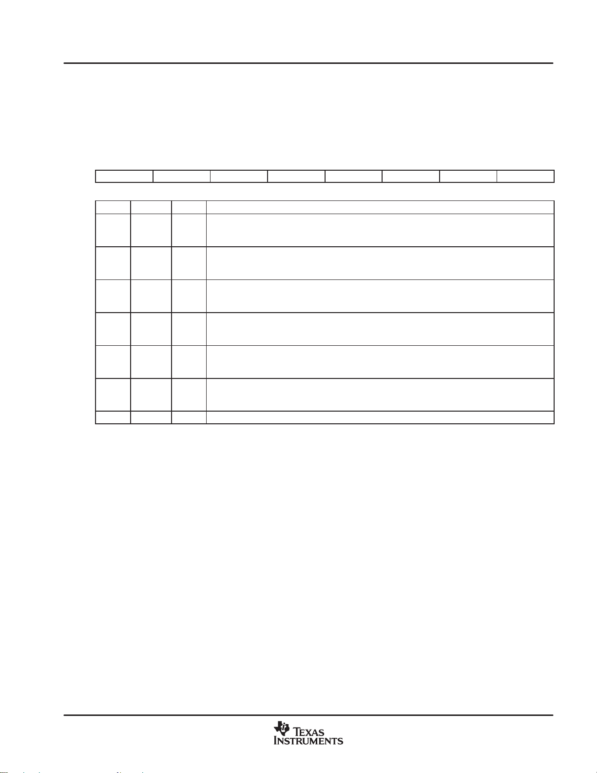
8.2 USBMSK: USB Interrupt Mask Register (XDATA at F007)
Bits[5:0] of the USBMSK register provide a mechanism to allow the MCU and firmware to enable or disable
the generation of certain types of interrupts based on the corresponding status or events that occurred.
The USBMSK register is cleared by a power up or a WDT reset. A USB reset cannot reset the USBMSK
register.
76543210
RSV RSV RSTR SUSPR RESUR WAKCLK SETUP STPOW
R/O R/O R/W R/W R/W R/W R/W R/W
BIT NAME RESET FUNCTION
0 STPOW 0 SETUP overwrite interrupt enable bit
1 SETUP 0 SETUP interrupt enable bit
2 WAKCLK 0 Wakeup clock interrupt enable.
3 RESUR 0 Function resume interrupt enable
4 SUSPR 0 Function suspend interrupt enable
5 RSTR 0 Function reset interrupt enable
7−6 RSV 00 Reserved. Application firmware must ensure these 2 bits are set to 00 during normal operation.
STPOW = 0 STPOW interrupt disabled
STPOW = 1 STPOW interrupt enabled
SETUP = 0 SETUP interrupt disabled
SETUP = 1 SETUP interrupt enabled
WAKCLK = 0 Wakeup clock interrupt disabled
WAKCLK = 1 Wakeup clock interrupt enabled
RESUR = 0 Function resume interrupt disabled
RESUR = 1 Function resume interrupt enabled
SUSPR = 0 Function suspend interrupt disabled
SUSPR = 1 Function suspend interrupt enabled
RSTR = 0 Function reset interrupt disabled
RSTR = 1 Function reset interrupt enabled
SLLS535D − November 2006 TUSB6250
8−3

8.3 USBSTA: USB Status Register (XDATA at F008)
Each bit in the USBSTA register can generate an interrupt if its corresponding mask bit is set in the USBMSK
register. The related interrupt is cleared when the corresponding status bit is cleared by the MCU except the
WAKCLK interrupt. All bits in this register are set by the hardware and can only be cleared by the MCU by
writing a 1 to the proper bit location (writing a 0 has no effect).
The USBSTA register (excluding the RSTR bit) is cleared by a power-up reset or a WDT reset. It can also be
cleared by a USB reset, when the function reset connection bit in the USBCTL register is set (FRSTE = 1).
The RSTR bit of the USBSTA register can only be cleared by a power-up reset or a WDT reset. A USB reset
sets this bit to 1.
76543210
RSV RSV RSTR SUSPR RESUR WAKCLK SETUP STPOW
R/O R/O R/C R/C R/C R/C R/C R/C
BIT
6−7 RSV 00 Reserved = 0
NAME RESET FUNCTION
0 STPOW 0 SETUP overwrite bit. Set by the hardware when the setup packet is received, while there is already
1 SETUP 0 SETUP transaction received bit. As long as SETUP is 1, IN and OUT on endpoint-0 are NAKed,
2 WAKCLK 0 Wakeup clock request bit. When W AKCLK interrupt is enabled, this bit is set in response to the status
3 RESUR 0 Function resume request bit. The MCU clears this bit by writing a 1 (writing 0 has no effect).
4 SUSPR 0 Function suspended request bit. This bit is set in response to a global or selective suspend condition.
5 RSTR 0 Function reset request bit. This bit is set in response to the host initiating a port reset to the TUSB6250.
a packet in the setup buffer. The MCU clears this bit by writing a 1 (writing 0 has no effect).
regardless of their real NAK bits value. The MCU clears this bit by writing a 1 (writing 0 has no effect).
change on any of these pins: VBUS, P3.4, P3.5, CD1
in turn wakes up the core clock if it has been shut down during suspend, when the remote wakeup is
enabled.
WAKCLK = 0 No wakeup clock event (status change on the five GPIO pins) is detected since the last
time the MCU clears the related status-change bit in USBWKUP.
WAKCLK = 1 Wakeup clock event (any status change on the five GPIO pins) is detected since the
last time the MCU clears the related status-change bit in USBWKUP.
RESUR = 0 No function resume is detected.
RESUR = 1 Function resume is detected.
The MCU clears this bit by writing a 1 (writing 0 has no effect).
SUSPR = 0 No function suspend is detected.
SUSPR = 1 Function suspend is detected.
The USB function reset is the condition to set this bit, not clear this bit. The MCU clears this bit by writing
a 1 (writing 0 has no effect).
RSTR = 0 No function reset is detected.
RSTR = 1 Function reset is detected.
, or CD2. The interrupt generated due to this bit
8.3.1 USB Suspend
The USB 2.0 specification requires that all USB devices must support the suspend state. The USB devices
begin the transition to the suspend state after they see a constant idle state on their upstream facing bus lines
for more than 3 ms. The device must actually be suspended, drawing only suspend current from the bus after
no more than 10 ms of bus inactivity on its port. The specification also requires that a device with remote
wakeup capability may not generate resume signaling, unless the bus has been continuously in the idle state
for 5 ms.
In other words, the specification allows all USB devices to enter suspend at any time between 3 ms to 10 ms
after bus idle. For USB high-speed capable devices, because there is an additional 0.125-ms revert-wait time
from high-speed to full-speed after 3-ms high-speed bus idle, the actual time to enter suspend is between
3.125 ms and 10 ms.
8−4
SLLS535D − November 2006TUSB6250

For the TUSB6250, the timing to enter the USB suspend is controlled by the application firmware running on
the embedded MCU. This flexibility allows the firmware to delay the time to go into suspend when the MCU
is currently busy on some tasks that must be finished before the suspend.
Because the firmware controls the time to enter the suspend, in order to be compliant with USB 2.0
specification, it is firmware responsibility to ensure that it clears the SUSPR interrupt status bit before 10 ms
expires.
The normal procedure during the bus idle and suspend condition is described as follows:
1. The TUSB6250 hardware detects 3-ms bus idle.
2. If the current USB bus connection is full speed, the TUSB6250 hardware sets the SUSPR bit in the
USBSTA register and generates an SUSPR (function suspend request) interrupt to the MCU.
If the current USB bus connection is high-speed, the TUSB6250 hardware reverts back to a full-speed
connection within 0.125 ms, then sets the SUSPR bit and generates the SUSPR interrupt.
3. The firmware can check whether there is any task that must be finished before the suspend and performs
it if desired. The firmware must ensure it grants the suspend request before 10 ms expires.
4. Once the firmware is ready to enter suspend, it clears the SUSPR bit in the USBSTA register. The
TUSB6250 hardware shuts the clock down (if LPEN = 1) and enters the suspend state.
8.3.2 WAKCLK Interrupt and Remote Wakeup
8.3.2.1 WAKCLK Interrupt Behavior
Figure 8−1 illustrates how the WAKCLK interrupt and WAKCLK status-change events are generated and
cleared. The top portion of the diagram shows how each of the WAKCLK status-change events causes the
WAKCLK bit in the USBSTA register to be set, if the WAKCLK interrupt is enabled in the USBMSK register
(for illustration purpose, WAKCLK_en = 1 in Figure 8−1 implies WAKCLK = 1 in USBMSK). The
VBUSCHG_det and the other three status-change event detection signals are generated internally by the
TUSB6250 hardware, whenever a WAKCLK status-change event occurs on the VBUS pin or the other four
remote wakeup capable port 3 GPIO pins (P3.2, P3.3, P3.4, and P3.5). These four status-change-event
detection signals, lasting one clock cycle, are ORed together to form a single cycle pulse to set the WAKCLK
bit in the USBSTA register, as long as the WAKCLK interrupt is enabled and the WAKCLK bit is not set.
Described below are important behaviors regarding the WAKCLK interrupt.
• The WAKCLK interrupt is triggered if any one of the four status-change events occurs, when the WAKCLK
bit is not yet set in USBSTA, the core clock is available, and the WAKCLK interrupt is enabled.
• The WAKCLK interrupt is shared among four different status-change events (interrupt sources). Before
the MCU clears the W AKCLK interrupt triggered by the first event, any new status-change event occurring
does not trigger a new WAKCLK interrupt. In other words, multiple status-change events only trigger o n e
WAKCLK interrupt before the MCU clears the existing WAKCLK residing in the interrupt queue.
• For the same reason, because the WAKCLK interrupt is shared, writing a 1 to the WAKCLK bit in the
USBSTA register clears the interrupt triggered by all the WAKCLK interrupt sources (status-change
events), although the individual status-change event bits are still kept in the USBWKUP register. In other
words, clearing one WAKCLK interrupt is like clearing all WAKCLK interrupts triggered by multiple
status-change events; although physically there is only one WAKCLK interrupt residing in the interrupt
queue.
• To avoid potential interrupt loss caused by mistaken writes, firmware developers must follow the
recommended procedure when servicing the WAKCLK interrupt. In summary, the WAKCLK bit must be
cleared before any status-change bit is cleared in the USBWKUP register.
− Once triggered by the W AKCLK interrupt, the firmware first must write a 1 to the WAKCLK bit in the
USBSTA register to clear the physical interrupt;
SLLS535D − November 2006 TUSB6250
8−5

− The firmware then performs a read to the USBWKUP register to reveal which status-change event bit
is set. If multiple events occurred, the firmware must service all of them individually.
− After servicing the WAKCLK interrupt for each individual status-change event, the firmware must write
a 1 to the corresponding bit in the USBWKUP register to clear such status-change event.
8.3.2.2 WAKCLK Interrupt Function During Normal Operation (When the TUSB6250 is not in
the USB Suspend State)
The WAKCLK interrupt provided by the TUSB6250 can be used for a variety of functions under different
operating conditions, other than just the remote wakeup interrupt in the suspend state. These functions can
include compact flash card detection, removable media insertion/eject, or an external event from another
on-board DSP as an end-product-specific-function, etc.
In other words, other than the VBUS status-change detection that has its fixed functionality, the other three
status-change events can be implemented as interrupt-specific to an end-product function as described
previously.
8.3.2.3 WAKCLK Interrupt Functions as a Remote Wakeup Interrupt (When the TUSB6250 is
in the USB Suspend State)
One common function of the WAKCLK interrupt is that it can be used as the remote wakeup interrupt. If the
TUSB6250 is in the USB suspend state, as long as the remote wakeup and the individual WAKCLK
status-change event detection (no need for VBUS detection, which is always enabled) are enabled, any VBUS
or status-change event causes the TUSB6250 to wake the core clock up, generate a WAKCLK interrupt to
the MCU, and send USB resume signaling to the upstream USB host. The resume signaling is sent by the
TUSB6250 hardware when either the WAKCLK interrupt is cleared by the firmware or 10 ms is reached after
the hardware triggers the WAKCLK interrupt to the MCU, whichever occurs first.
It is important to understand that all USB devices only report to the upstream USB host whether they are
remote wakeup capable. It is up to the USB host to decide whether to enable a USB device’s remote wakeup
capability through the Set_Feature command.
The TUSB6250 offers a unique feature that allows its remote wakeup capability to be disabled, while the
TUSB6250 is still able to capture and remember the status-change event that occurred during the USB
suspend state.
When the TUSB6250 is in the suspend state, with the remote wakeup disabled (RWUPEN bit of the USBCTL
register is cleared), the following two scenarios describe whether and how the core clock of the TUSB6250
is awakened due to the WAKCLK status-change event.
• If the low-power enable bit (LPEN) is not set in the USBCTL register, the TUSB6250 has no need to wake
the clock up, because the clock is not disabled and is still running during suspend. Any valid WAKCLK
status-change event can cause a WAKCLK interrupt to be generated. This normally happens for a
self-powered application.
• If the low-power enable bit (LPEN) is set in the USBCTL register, the core clock is shut down during
suspend. The WAKCLK interrupt event that occurred during suspend is captured and remembered using
asynchronous logic, however no interrupt is triggered. The TUSB6250 keeps the core clock shut down
and remains in the suspended state until the core clock is available, which is when the USB host signals
resume to the TUSB6250. When the core clock is available, the remembered W AKCLK event triggers the
actual interrupt.
8−6
SLLS535D − November 2006TUSB6250

WAKCLK_en
VBUSCHG_det
CDCHG_det
P34CHG_det
P35CHG_det
Write 1 to Clear
the WAKCLK Bit)
Write 1 to Clear
the P35CHG Bit)
DQ
ENZ
Q
DQ
ENZ
Q
WAKCLK Bit
in USBSTA
P35CHG Bit
in USBWKUP
Write 1 to Clear
the P34CHG Bit)
60-MHz
Core CLK
Write 1 to Clear
the CDCHG Bit)
DQ
ENZ
Q
DQ
ENZ
Q
DQ
P34CHG Bit
in USBWKUP
CDCHG Bit
in USBWKUP
VBUSCHG Bit
in USBWKUP
ENZ
Write_1 to Clear
the VBUSCHG Bit)
Q
Figure 8−1. WAKCLK Interrupt and Wakeup Status-Change Illustration Logical Diagram
SLLS535D − November 2006 TUSB6250
8−7

8.3.2.4 Register Settings Affect the WAKCLK Interrupt
The seven enable bits listed in Table 8−1 greatly affect the behavior and function of the WAKCLK interrupt
function.
Table 8−1. Register Setting for the WAKCLK Interrupt and Remote Wakeup
BIT NAME
LPEN USBCTL[6]
WAKCLK USBMSK[2]
RWUPEN USBCTL[5]
P34STEN MCUCNFG[2]
P35STEN MCUCNFG[3]
CD1STEN MCUCNFG[4]
CD2STEN MCUCNFG[5]
BIT LOCATION
IN REGISTER
FUNCTION CONTROLLED
Low-power enable.
LPEN controls whether the core clock of the TUSB6250 is shut down when the TUSB6250 enters the USB
suspend state.
WAKCLK interrupt enable. WAKCLK controls:
Whether the WAKCLK interrupt is generated when VBUS or any other status-change events occur.
Whether the core clock of the TUSB6250 is awakened in the suspend state along with the RWUPEN bit
setting.
Remote wakeup enable. RWUPEN controls:
Whether the core clock of the TUSB6250 is awakened in the suspend state along with the WAKCLK bit
setting.
Whether the USB resume signaling is sent to the upstream USB host when any remote wakeup event occurs
at either the VBUS pin or any of the four remote wakeup-capable GPIOs.
GPIO port3.4 status-change detection enable.
P34STEN allows the firmware to enable/disable the status-change detection on the port3.4 pin.
GPIO port3.5 status-change detection enable.
P35STEN allows the firmware to enable/disable the status-change detection on the port3.5 pin.
Card detection-1 status-change enable.
CD1STEN allows the firmware to enable/disable the status-change detection on the port3.2 pin.
Card detection-2 status-change enable.
CD2STEN allows the firmware to enable/disable the status-change detection on the port3.3 pin.
In summary, to configure the WAKCLK interrupt and remote wakeup, it is important to ensure that:
• When the remote wakeup is desired (this means sending resume signaling to the host is desired), both
WAKCLK and RWUPEN must be set.
• If the remote wakeup is not desired (this means no resume signaling to the host is desired), while the
end-product application cannot afford losing any status-change event that might occur when the
TUSB6250 is i n the USB suspend state, the WAKCLK bit can be set, and the RWUPEN bit can be disabled.
8−8
SLLS535D − November 2006TUSB6250

8.4 FUNADR: Function Address Register (XDATA at F009)
The FUNADR register contains the current setting of the USB device address assigned to the USB function
of the TUSB6250 by the USB host. After a power-up reset or a USB reset, the default function address is 00h.
During the enumeration of the USB function of the TUSB6250 by the host, the MCU and firmware load the
assigned address from the host to the FA[6:0] bits of the FUNADR register on receiving a USB Set_Address
request at the control endpoint.
The HS bit of the FUNADR register reflects the TUSB6250’s current connection speed on the USB bus.
The FUNADR register is cleared by a power-up reset, a WDT reset, or a USB reset (regardless of whether
the function reset connection bit is set in the USBCTL register).
76543210
HS FA6 FA5 FA4 FA3 FA2 FA1 FA0
R/O R/W R/W R/W R/W R/W R/W R/W
BIT
6−0 FA[6:0] 0000000 These bits define the current device address assigned to the function. The MCU writes a value to this
NAME RESET FUNCTION
register as a result of the SET-ADDRESS host command.
7 HS 0 High-speed connection status. This bit reflects the type of USB connection speed on the upstream
transceivers. This bit is set automatically by the transceiver selection logic and the MCU can only read
this bit.
HS = 0 Indicates full-speed connection
HS = 1 Indicates high-speed connection
8.5 UTMICFG: UTMI Configuration Status Register (XDATA at F00A)
The UTMICFG register provides the current status of the UTMI configuration of the integrated USB 2.0
UTMI-compliant PHY.
The UTMICFG register is cleared by a power-up reset or a WDT reset. A USB reset cannot clear the UTMICFG
register.
765 4 3 2 1 0
SUSPNST VBUS XCVR_SEL TERM_SELECT LINE_STATE1 LINE_STATE0 OP_MOD1 OP_MOD0
R/O R/O R/O R/O R/O R/O R/O R/O
BIT
1−0 OP_MOD[1:0] 01 These bits define the current device operation mode to USB 2.0 PHY.
3−2 LINE_STATE[1:0] Bus This bit reflects the current line_state on DP and DM. (See Note 1)
4 TERM_SELECT 1 USB 2.0 transceiver termination select.
5 XCVR_SEL 1 USB 2.0 transceiver select.
6 VBUS Bus VBUS status. (See Note 1)
7 SUSPNST 0 Suspend status. This bit, when set, indicates the TUSB6250 is currently in USB suspend
NOTE 1: The reset value for both the LINE_STATE and VBUS are denoted as bus, which means that their actual reset value depends
NAME RESET FUNCTION
TERM_SELECT = 0 HS termination is enabled.
TERM_SELECT = 1 FS termination is enabled.
XCVR_SEL = 0 HS transceiver is enabled.
XCVR_SEL = 1 FS transceiver is enabled.
VBUS = 0 VBUS power is not present.
VBUS = 1 VBUS power is present.
state. Whether or not the core clock is still running depends on the setting of the LPEN bit
in the USBCTL register.
SUSPNST = 0 The TUSB6250 is not in the USB suspend state.
SUSPNST = 1 The TUSB6250 is in the USB suspend state.
on the actual condition of the USB bus data line and VBUS during reset.
SLLS535D − November 2006 TUSB6250
8−9

8.6 USBFCL: USB Frame Counter Low-Byte Register (XDATA at F00B)
The USBFCL register contains the read-only USB frame counter low-byte value of the 11-bit frame number
value received from the USB host in the start-of-frame packet. The frame number bit values are updated by
the hardware for each USB frame with the frame number field value received in the USB start-of-frame packet.
The frame number can be used as a time stamp by the USB function. If the frame number of the TUSB6250
is not locked to the USB host frame timer, then the frame number is incremented from the previous value when
a pseudo start-of-frame occurs.
The USBFCL register is cleared by a power-up reset or a WDT reset. A USB reset cannot clear the USBFCL
register.
76543210
FRAMNUM7 FRAMNUM6 FRAMNUM5 FRAMNUM4 FRAMNUM3 FRAMNUM2 FRAMNUM1 FRAMNUM0
R/O R/O R/O R/O R/O R/O R/O R/O
BIT
7−0 FRAMNUM[7:0] 00h These bits indicate the frame number lower-order 8-bit value.
NAME RESET FUNCTION
8.7 USBFCH: USB Frame Counter High-Byte Register (XDATA at F00C)
The FRAMNUM[10:8] bits of the USBFCH register contain the read-only USB frame counter high-byte value
of the 11-bit frame number value received from the USB host in the start-of-frame packet. The UFRMNUM[2:0]
bits contain the read-only micro frame number.
The USBFCH register is cleared by a power-up reset or a WDT reset. A USB reset cannot clear the USBFCH
register.
765432 10
RSV RSV UFRAMNUM2 UFRAMNUM1 UFRAMNUM0 FRAMNUM10 FRAMNUM9 FRAMNUM8
R/O R/O R/O R/O R/O R/O R/O R/O
BIT
2−0 FRAMNUM[10:8] 000 These bits indicate the frame number higher-order 3-bit value.
5−3 UFRAMNUM[2:0] 000 These three bits indicate the microframe number.
7−6 RSV 00 Reserved. The application firmware must ensure these two bits are set to 00 during normal
NAME RESET FUNCTION
operation.
8.8 USBWKUP: USB Wake-Up Reason Register (XDATA at F00D)
The USBWKUP register indicates the USB wakeup event reason (source) from the embedded MCU’s port-3
GPIO pins and VBUS pin.
8−10
All four status-change bits (P34CHG, P35CHG, VBUSCHG, and CDCHG) in the USBWKUP register are set
individually by the hardware when their corresponding enable bit is set in the MCUCNFG register (at ESFR
FCh), with the exception that VBUSCHG is always enabled. They can be cleared by the MCU writing a 1 to
the proper bit location (writing a 0 has no effect). In addition, the OR-result of these four status-change bits,
when set, generates the WAKCLK interrupt if the interrupt is enabled in the USBMSK register (R/C notation
indicates read and set-to-clear only by the MCU).
Any status-change bit, when set, indicates there is a status-change event that occurred since the last time the
MCU cleared the same status-change bit. Below are important notes regarding the consecutive status-change
events that occur before the MCU services and clears the current WAKCLK interrupt, assuming the related
status-change event is enabled in the MCUCNFG register.
• As described in Section 8.3.2, WAKCLK Interrupt and Remote Wakeup, regardless if the new
status-change event occurring is the same as the one that already occurred, consecutive status-change
SLLS535D − November 2006TUSB6250

events do not trigger a new WAKCLK interrupt if there is already a WAKCLK interrupt in the queue. This
avoids the MCU being interrupted by too many WAKCLK interrupts.
• Following the same guideline, when consecutive status-change events happen:
− If the source of the new status-change event that occurred is different from the ones that already
occurred, the new status-change event is logged in the corresponding status-change bit of the
USBWKUP register. For example, if the CDCHG bit is already set, but VBUSCHG bit is not set, a new
VBUS status change causes the VBUSCHG bit to be set, although it might not trigger a new W AKCLK
interrupt if the current WAKCLK interrupt is still in the queue.
− If the source of the new status-change event occurred is the same as the ones that already occurred,
the new status-change event is ignored. For example, if CDCHG bit is still set, but a new CDCHG
event is detected, the new CDCHG status-change event is ignored. This avoids unnecessary
changes in the status-change bits of the USBWKUP register caused by redundant status-change
events.
• For detailed information regarding the WAKCLK interrupt, see Section 8.3.2, WAKCLK Interrupt and
Remote Wakeup.
• Even if the WAKCLK interrupt is not enabled, the status-change events can still be observed by polling
the MCUCNFG register, as long as the event detection is enabled in the MCUCNFG register.
The CD1STEN and CD2STEN bits in the MCUCNFG register can be individually enabled for separate wakeup
event detection. However, because these two bits share the same status-change indication bit (CDCHG) in
the USB wakeup reason register, clearing one interrupt source results in the interrupt source indication of the
other being cleared at the same time.
To avoid missing status changes on the port-3 GPIO, especially in the suspend condition in which the clock
may be shut down, the following two sets of circuitries are used for generating the four status-change bits (bit
7 to 4).
• Debounced status-change circuitry is used whenever the clock is available and stable. The debouncing
time interval is 1.28 ms, which means that only switching lasting longer than 1.28 ms is considered a valid
logic transition on the related port-3 GPIO pin.
• Asynchronously triggered status-change circuitry is used to latch the change event when the remote
wakeup is disabled and the low-power enable is true (LPEN bit in USBCTL is set), while the TUSB6250
is in the suspend state.
Bits[3:0] provide the debounced read-only value of the current logic level on the corresponding GPIO pins of
port 3. The debouncing time interval is 1.28 ms.
The USBWKUP register is cleared by a power-up reset or a WDT reset. A USB reset cannot clear the
USBWKUP register.
76543210
P35CHG P34CHG VBUSCHG CDCHG P35ST P34ST CD2ST CD1ST
R/C R/C R/C R/C R/O R/O R/O R/O
BIT
SLLS535D − November 2006 TUSB6250
NAME RESET FUNCTION
0 CD1ST 1 Compact flash card/media detection CD1 status bit. This bit represents the debounced status value
1 CD2ST 1 Compact flash card/media detection CD2 status bit. This bit represents the debounced status value
on the CD1
CD1ST = 1 CF card/media is not inserted.
CD1ST = 0 CF card/media may be inserted (a firm insertion depends on the status on both media
on the CD2
CD2ST = 1 CF card/media is not inserted.
CD2ST = 0 CF card/media may be inserted (a firm insertion depends on the status on both media
pin.
detection pins).
pin.
detection pins).
8−11

BIT FUNCTIONRESETNAME
IN/OUT
IN/OUT
2 P34ST 0 P3.4 status bit. This bit represents the debounced status value on the P3.4 pin.
3 P35ST 0 P3.5 status bit. This bit represents the debounced status value on the P3.5 pin.
4 CDCHG 0 Compact flash card/media detection pin status-change bit. This bit, when set, indicates a status
change occurred at either the CD1
to ensure a correct media insertion.
CDCHG = 0 No CF card/media detection status change occurred.
CDCHG = 1 CF card/media detection status change occurred on at least one CD pin.
5 VBUSCHG 0 VBUS status-change bit.
VBUSCHG = 0 No VBUS status change occurred.
VBUSCHG = 1 A VBUS status change occurred.
6 P34CHG 0 P34CHG status-change bit.
P34CHG = 0 No P3.4 pin status change occurred.
P34CHG = 1 A P3.4 pin status change occurred.
7 P35CHG 0 P35CHG status-change bit.
P35CHG = 0 No P3.5 pin status change occurred.
P35CHG = 1 A P3.5 pin status change occurred.
8.9 Endpoint-0 Descriptor Registers
All EDBs (endpoint descriptor block, including EDB-0 and EDB-1 to EDB-4) are implemented in registers.
Their respective endpoint data buffers are implemented in SPRAM. Table 8−2 defines the registers and their
respective address used for EDB-0.
EDB-0 has no base-address register, because these addresses are hardwired and depend on the
configuration set by the BZ[1:0] bits in the IEPCNFG_0 register (see Table 8−3).
or CD2 pin. The firmware must read the status of these two pins
Table 8−2. Input/Output EDB-0 Registers
ADDRESS REGISTER NAME DESCRIPTION
F004 OEPBCNX_0 Output endpoint_0: X-buffer byte-count register
F003 OEPCNFG_0 Output endpoint_0: configuration register
F001 IEPBCNX_0 Input endpoint_0: X-buffer byte-count register
F000 IEPCNFG_0 Input endpoint_0: configuration register
Table 8−3. Input/Output EDB-0 Buffer Location as Defined by BZ[1:0]
DBUF=0 BZ[1:0]=0 BZ[1:0]=1 BZ[1:0]=2 BZ[1:0]=3
ENDPOINT-0
Input
Output
SIZE (BYTES) = 8 16 32 64
End address E00F E01F E03F E07F
IEP0BA = E008 E010 E020 E040
End address E007 E00F E01F E03F
OEP0BA = E000 E000 E000 E000
8−12
SLLS535D − November 2006TUSB6250

8.9.1 IEPCNFG_0: Input Endpoint-0 Configuration Register (XDATA at F000)
The IEPCNFG_0 register contains various bits used to configure and control this endpoint.
76543210
UBME NAK_INTE TOGLE RSV STALL USBIE BZ
R/W R/W R/O R/O R/W R/W R/W R/W
BIT NAME RESET FUNCTION
1−0 BZ[1:0] 00b Endpoint-0 bu f fer size for IN and OUT transaction. The value of this field also defines the starting address
of the input buffer. See Table 8−3.
00 = 8 bytes
01 = 16 bytes
10 = 32 bytes
11 = 64 bytes
2 USBIE 0 USB interrupt enable on transaction completion. Set/cleared by the MCU.
USBIE = 0 No interrupt
USBIE = 1 Interrupt on transaction completion
3 STALL 0 USB stall condition indication. Set/cleared by the MCU.
STALL = 0 No stall
STALL = 1 USB stall condition. If set by the MCU, a STALL handshake is initiated and the bit is cleared
automatically by the next setup transaction.
4 RSV 0 Reserved
5 TOGLE 0 USB toggle bit. The hardware resets this bit when the setup packet is received.
6 NAK_INTE 0 NAK interrupt enable
NAK_INTE = 0 NAK does not trigger interrupt.
NAK_INTE = 1 NAK triggers an interrupt.
7 UBME 0 UBM enable/disable bit. Set/cleared by the MCU.
UBME = 0 UBM cannot use this endpoint.
UBME = 1 UBM can use this endpoint.
1
BZ
0
8.9.2 IEPBCN_0: Input Endpoint-0 Buffer Byte-Count Register (XDATA at F001)
The IEPBCN_0 register contains the NAK bit and the 7-bit value used to specify the amount of data to be
transmitted in a data packet to the USB host.
76543210
NAK C6 C5 C4 C3 C2 C1 C0
R/W R/W R/W R/W R/W R/W R/W R/W
BIT NAME RESET FUNCTION
6−0 C[6:0] 0000000 Byte count. Only count of 0 to 64 (00h to 40h) is supported.
7 NAK 1 NAK=0 Buffer contains a valid packet for Host-IN request.
00h Byte count = 0
:
40h Byte count = 64
41h to 7Fh should not be used. If the MCU writes any value greater than 0x40 to C[6:0], the TUSB6250
hardware corrects it and only writes 0x40 to C[6:0].
NAK=1 Buffer is empty (TUSB6250 NAKs the host-IN request).
SLLS535D − November 2006 TUSB6250
8−13

8.9.3 OEPCNFG_0: Output Endpoint-0 Configuration Register (XDATA at F003)
The OEPCNFG_0 register contains various bits used to configure and control this endpoint.
76543210
UBME NAK_INTE TOGLE RSV STALL USBIE RSV RSV
R/W R/W R/O R/O R/W R/W R/O R/O
BIT NAME RESET FUNCTION
1−0 RSV 00 Reserved = 00
2 USBIE 0 USB interrupt enable on transaction completion. Set/cleared by the MCU.
3 STALL 0 USB stall condition indication. Set/cleared by MCU.
4 RSV 0 Reserved = 0
5 TOGLE 0 USB toggle bit
6 NAK_INTE 0 NAK interrupt enable
7 UBME 0 UBM enable/disable bit. Set/cleared by the MCU.
USBIE = 0 No interrupt
USBIE = 1 Interrupt on transaction completion
STALL = 0 No stall
STALL = 1 USB stall condition. If set by the MCU, a STALL handshake is initiated and the bit is
cleared automatically.
NAK_INTE = 0 NAK does not trigger an interrupt.
NAK_INTE = 1 NAK triggers an interrupt.
UBME = 0 UBM cannot use this endpoint.
UBME = 1 UBM can use this endpoint.
8.9.4 OEPBCN_0: Output Endpoint-0 Buffer Byte-Count Register (XDATA at F004)
The OEPBCN_0 register contains the NAK bit and a 7-bit value used to specify the amount of data received
in a data packet from the USB host.
76543210
NAK C
R/W R/O R/O R/O R/O R/O R/O R/O
BIT
NAME RESET FUNCTION
6−0 C[6:0] 0000000 Byte count. Only count of 0 to 64 (00h to 40h) is supported.
7 NAK 0 NAK = 0 Buffer is empty and ready for a host-out request.
6
00h Byte count = 0
:
40h Byte count = 64
41h to 7Fh should not be used. If the USB host sends more than 64 bytes of data to this endpoint, the
TUSB6250 hardware treats it as an illegal packet. When this condition happens, the hardware does not
update the byte count in the OEBPCN_0 register if it contains the value from the previous packet. There
is no ACK or NAK response generated by the hardware. The MCU is not informed with the arrival of this
illegal packet.
NAK = 1 Buffer contains a valid packet from host (TUSB6250 NAKs the host-OUT request).
C
5
C
4
C
3
C
2
C
1
C
0
8−14
SLLS535D − November 2006TUSB6250

Table 8−4 shows the buffer location address map for a single buffer with a buffer size of 64 bytes.
TOPBUFF
↑
|
Table 8−4. EDB0 Buffer Locations (in SPRAM)
ADDRESS NAME DESCRIPTION
EFFF
↑
TOPBUFF
Top of buffer space
|
|
|
|
Buffer space
4K – 128 bytes free
|
↓
E080
E07F ↑
↑
|
↓
E040 ↓
E03F
↑
|
↓
E000
NOTE: This table is based on a single buffer with a buffer size of 64 bytes
for both input and output endpoint-0.
64 bytes
64 bytes
Input endpoint_0, buffer
Output endpoint_0, buffer
I
I
↑
I
|
↓
8.10 Endpoint Descriptor Block (EDB-1 to EDB-4)
The endpoint descriptor block (EDB) defines the endpoint characteristics for data transfer between the USB
and the UBM. Four input and four output endpoints are provided. All EDBs are implemented in
memory-mapped registers as defined in Table 6−2.
Double data buffers are provided for EDB-1 to EDB-4 (both input and output endpoints). The firmware in the
MCU decides whether to use the double data buffers by writing to the DBUF bit in the IEPCNFG_n and
OEPCNFG_n registers. The double data buffer is disabled by default (DBUF = 0). In this case, only the primary
data buffer (X-buffer) is enabled.
Each EDB contains information describing the X and Y-buffers. In addition, it provides general status
information. Figure 8−2 and Figure 8−3 illustrate how the IN_Endpoint_number (E[2:0]) and
OUT_Endpoint_number (E[2:0]) are used to generate the index (address) to the input EDB and the output
EDB, respectively, in the MMR memory map. Note that A[3] is used to distinguish between input and output.
Table 8−5 illustrates each EDB entry (register) for EDB-1 to EDB-4.
Figure 8−4 illustrates how the complete 16-bit EDB-buffer base address within the MMR memory map is
generated in the TUSB6250 hardware for each EDB data buffer.
As defined in the USB 2.0 specification, the maximum packet size is 512 bytes for a high-speed bulk endpoint
and 64 bytes for a full-speed bulk endpoint.
Endpoint # IN
Bit Value 1 1 1 1 0 0 0 0 0 E2 E1 E0 0 0 0 0
Bit Number A15 A14 A13 A12 A11 A10 A9 A8 A7 A6 A5 A4 A3 A2 A1 A0
Figure 8−2. IN-Endpoint Index Generation
SLLS535D − November 2006 TUSB6250
8−15

Endpoint # OUT
Bit Value 1 1 1 1 0 0 0 0 0 E2 E1 E0 1 0 0 0
Bit Number A15 A14 A13 A12 A11 A10 A9 A8 A7 A6 A5 A4 A3 A2 A1 A0
Figure 8−3. OUT-Endpoint Index Generation
Table 8−5. EDB Entries in MMR (n = 1 to 4)
OFFSET
(see Note 2)
07 EPBCNHY_n I/O endpoint_n: Y byte-count (HB) register
06 EPBCNLY_n I/O endpoint_n: Y byte-count (LB) register
05 EPBBADRY_n I/O endpoint_n: Y-buffer base address register (see Note 1)
04 EPSIZXY_n I/O endpoint_n: X/Y-buffer size register
03 EPBCNHX_n I/O endpoint_n: X byte-count (HB) register
02 EPBCNLX_n I/O endpoint_n: X byte-count (LB) register
01 EPBBADRX_n I/O endpoint_n: X-buffer base address register (see Note 1)
00 EPCNFG_n I/O endpoint_n: configuration register
NOTES: 1. The entry contains the A[11:4] portion of a 16-bit address. See Figure 8−4.
2. Offset number is based on the A[2:0] value.
Inserted by Hardware Base Address in EDB Inserted by Hardware
Bit Value 1 1 1 0 A11 A10 A9 A8 A7 A6 A5 A4 0 0 0 0
Bit Number 15 14 13 12 11 10 9 8 7 6 5 4 3 2 1 0
ENTRY NAME DESCRIPTION
Figure 8−4. 16-Bit EDB Data Buffer Address Generation From the Value of the Buffer Base Address
8−16
SLLS535D − November 2006TUSB6250

8.10.1 IEPCNFG_n: Input Endpoint Configuration Register (n = 1 to 4) (XDATA at
F010, F020, F030, F040)
The IEPCNFG register contains various bits used to configure and control the specified endpoint.
76543210
UBME NAK_INTE TOGLE DBUF STALL USBIE RST_TOGLE MAP_SECF
R/W R/W R/O R/W R/W R/W W/O R/W
BIT NAME RESET FUNCTION
0 MAP_SECF 0 Map data buffer to sector FIFO RAM.
1 RST_TOGLE 0 Reset TOGLE bit. This bit always returns 0 when read by the MCU.
2 USBIE 0 USB interrupt enable on transaction completion
3 STALL 0 USB stall condition indication.
4 DBUF 0 Double buffer enable for input endpoint_n.
5 TOGLE 0 USB toggle bit. This read-only bit reflects the toggle sequence bit of DATA0, DATA1. The actual
6 NAK_INTE 0 NAK interrupt enable
7 UBME 0 UBM enable/disable bit. Set/cleared by the MCU.
MAP_SECF = 0 Endpoint data is stored in 4K-byte endpoint data buffer.
MAP_SECF = 1 Endpoint data is stored in sector FIFO RAM.
The MCU writes a 1 to this bit in order to reset the TOGLE bit (bit 5) to 0.
USBIE = 0 No interrupt
USBIE = 1 Interrupt on transaction completion
STALL= 0 No stall
STALL= 1 USB stall condition. If set by the MCU, a STALL handshake is initiated.
DBUF= 0 Primary buffer only (X-buffer only)
DBUF= 1 TOGLE-bit selects X or Y-buffer
response from the TUSB6250 also depends on the related STALL and NAK bits. The hardware
updates the TOGLE bit automatically.
TOGLE = 0 The TUSB6205 expects the next in-transfer data packet PID to be DATA0.
TOGLE = 1 The TUSB6205 expects the next in-transfer data packet PID to be DATA1.
NAK_INTE = 0 NAK does not trigger an interrupt.
NAK_INTE = 1 NAK triggers an interrupt.
UBME = 0 UBM cannot use this endpoint.
UBME = 1 UBM can use this endpoint
8.10.2 IEPBBADRX_n: Input Endpoint X-Buffer Base Address Register (n = 1 to 4)
(XDATA at F011, F021, F031, F041)
The IEPBBADRX_n register contains the X-buffer base address for the specified input endpoint.
76543210
A11 A10 A9 A8 A7 A6 A5 A4
R/W R/W R/W R/W R/W R/W R/W R/W
BIT
7−0 A[11:4] 00h This is the middle 8-bit value of the complete (1110 & A[11:4] & 0000) 16-bit X-buffer base address.
SLLS535D − November 2006 TUSB6250
NAME RESET FUNCTION
See Figure 8−4. This value can be set only by the MCU. The UBM or MCU uses this value as the start
address of the X-buffer for a given transaction.
8−17

8.10.3 IEPBCNLX_n: Input Endpoint X-Buffer Byte-Count Low-Byte Register (n = 1
to 4) (XDATA at F012, F022, F032, F042)
The IEPBCNLX_n register contains the lower 8-bit value in the X-buffer that is used to specify the amount of
data to be transmitted in a data packet to the USB host.
76543210
C7 C6 C5 C4 C3 C2 C1 C0
R/W R/W R/W R/W R/W R/W R/W R/W
BIT
7−0 C[7:0] 00h X-buffer byte-count: low byte
NAME RESET FUNCTION
8.10.4 IEPBCNHX_n: Input Endpoint X-Buffer Byte-Count High-Byte Register (n = 1 to
4) (XDATA at F013, F023, F033, F043)
The IEPBCNHX_n register contains the NAK bit and the higher 3-bit value in the X-buffer that is used to specify
the amount of data to be transmitted in a data packet to the USB host.
76543210
NAK RSV RSV RSV RSV C10 C9 C8
R/W R/O R/O R/O R/O R/W R/W R/W
BIT
2−0 C[10:8] 0 X-buffer byte count higher 3 bits. These bits in combination with C[7:0] provide the byte count of a given
6−3 RSV 0 Reserved = 0
Following is the procedure to be used by the firmware when using the NAK bit for flow-control handshake. For
the purpose of illustration, it is assumed that the double buffer (DBUF) is enabled. If DBUF is not enabled, the
X-buffer is always used regardless of the value of the data packet PID of the coming in-transfer.
NAME RESET FUNCTION
transaction (count = 0 to 2047).
7 NAK 0 NAK bit is used as flow control handshake for X-buffer.
NAK = 0 This bit is cleared to 0 by the firmware to indicate that the endpoint data buffer contains a
valid packet for Host-IN request.
NAK = 1 This bit is set to 1 by the TUSB6250 hardware to indicate that the endpoint data buffer is empty
(TUSB6250 NAKs the Host-IN request).
8−18
1. The first in-transfer comes when the in-endpoint buffer is empty (data payload not ready for the in-transfer
received) and NAK =1. The TUSB6250 responds to the in-transfer with a NAK handshake and starts
preparing the data payload required for this in-transfer.
2. The MCU is alerted with a NAK interrupt to the current in-endpoint. The firmware loads the data into either
the X-buffer or Y-buffer depending on the following conditions:
− If DBUF = 1, TOGLE = 0, and the data PID = DATA0:
The firmware loads the data into the X-buffer of the endpoint data buffer (4K bytes EDB) and updates
the X-buffer byte-count information in IEPBCNLX_n and IEPBCNHX_n registers.
− If DBUF = 1, TOGLE = 1 and the data PID = DATA1:
The firmware loads the data into the Y-buffer of the endpoint data buffer (4K byte EDB) and updates
the Y-buffer byte-count information in the IEPBCNLY_n and IEPBCNHY_n registers.
3. The firmware then clears the NAK bit to 0 to indicate to the TUSB6250 hardware that a valid data packet
with the specified byte count is ready to be transmitted to the USB host.
4. The TUSB6250 hardware sends the data packet in the specified length on the USB host sending the next
IN-request with a valid IN-token.
SLLS535D − November 2006TUSB6250

5. Once the USB host acknowledges the host-IN transfer with an ACK, the TUSB6250 hardware sets the
NAK bit to 1, so that any new host-IN request is NAKed until the MCU and firmware get the new required
data payload ready.
8.10.5 IEPSIZXY_n: Input Endpoint X/Y-Buffer Size Register (n = 1 to 4) (XDATA at
F014, F024, F034, F044)
The IEPSIZXY register contains the X- and Y-buffer size for the specified input endpoint.
76543210
S10 S9 S8 S7 S6 S5 S4 S3
R/W R/W R/W R/W R/W R/W R/W R/W
BIT
7−0 S[10:3] 00h X- and Y-buffer size in byte: S[2:0] is padded with zeros (S[10:3] & 000) to produce an 11-bit value.
NAME RESET FUNCTION
Size is 0 to 1024 in increments of eight.
8.10.6 IEPBBADRY_n: Input Endpoint Y-Buffer Base Address Register (n = 1 to 4)
(XDATA at F015, F025, F035, F045)
The IEPBBADRY_n register contains the Y-buffer base address for the specified input endpoint.
76543210
A11 A10 A9 A8 A7 A6 A5 A4
R/W R/W R/W R/W R/W R/W R/W R/W
BIT
7−0 A[11:4] 00h This is the middle 8-bit value of the complete (1110 & A[11:4] & 0000) 16-bit Y-buffer base address.
NAME RESET FUNCTION
See Figure 8−4. This value is set by the MCU. The UBM or the MCU uses this value as the start
address of the Y-buffer for a given transaction.
8.10.7 IEPBCNLY_n: Input Endpoint Y-Buffer Byte-Count Low-Byte Register (n = 1 to
4) (XDATA at F016, F026, F036, F046)
The IEPBCNLY_n register contains the lower 8-bit value in the Y-buffer that is used to specify the amount of
data to be transmitted in a data packet to the USB host.
76543210
C7 C6 C5 C4 C3 C2 C1 C0
R/W R/W R/W R/W R/W R/W R/W R/W
BIT
7−0 C[7:0] 00h Y-buffer byte-count: low byte
SLLS535D − November 2006 TUSB6250
NAME RESET FUNCTION
8−19

8.10.8 IEPBCNHY_n: Input Endpoint Y-Buffer Byte-Count High-Byte Register (n = 1
to 4) (XDATA at F017, F027, F037, F047)
The IEPBCNHY_n register contains the NAK bit and the higher 3-bit value in the Y-buffer that is used to specify
the amount of data to be transmitted in a data packet to the USB host. See the procedure described in the
IEPBCNHX_n register when using the NAK bit for flow control handshake.
76543210
NAK RSV RSV RSV RSV C10 C9 C8
R/W R/O R/O R/O R/O R/W R/W R/W
BIT
2−0 C[10:8] 000 Y-buffer byte count higher 3 bits. These bits, in combination with C[7:0], provide the byte count of a
6−3 RSV 0000 Reserved = 0
NAME RESET FUNCTION
given transaction (count = 0 to 2047).
7 NAK 0 NAK bit is used as flow control handshake for Y-buffer.
NAK = 0 Buffer contains a valid packet for the Host-IN request.
NAK = 1 Buffer is empty (TUSB6250 NAKs the host-IN request).
8.10.9 OEPCNF_n: Output Endpoint Configuration Register (n = 1 to 4) (XDATA at
F018, F028, F038, F048)
The OEPCNF_n register contains various bits used to configure and control the specified endpoint.
76543210
UBME NAK_INTE TOGLE DBUF STALL USBIE RS_TOGLE MAP_SECF
R/W R/W R/O R/W R/W R/W W/O R/W
BIT
0 MAP_SECF 0 Map data buffer to sector FIFO RAM. The MCU writes to this bit to inform the state machine
1 RST_TOGLE 0 Reset TOGLE. This bit always returns 0 when read by the MCU.
2 USBIE 0 USB interrupt enable on transaction completion. Set/cleared by the MCU.
3 STALL 0 USB stall condition indication.
4 DBUF 0 Double buffer enable for output endpoint_n.
5 TOGLE 0 USB toggle bit. This read-only bit reflects the toggle sequence bit of DATA0, DATA1. The actual
6 NAK_INTE 0 NAK interrupt enable
7 UBME 0 UBM enable/disable bit. Set/cleared by the MCU.
NAME RESET FUNCTION
whether it wants the data to be transferred/stored in either the 4K-byte EDB buffer or the sector
FIFO. If the sector FIFO is selected, when the data transfer phase is over, the state machine
automatically switches the data storage area back to the 4K-byte EDB buffer.
MAP_SECF = 0 Endpoint data is stored in the 4K-byte endpoint data buffer.
MAP_SECF = 1 Endpoint data is stored in the sector FIFO RAM.
The MCU can write a 1 to this bit in order to reset the TOGLE bit (bit 5) to ‘0’.
USBIE = 0 No interrupt
USBIE = 1 Interrupt on transaction completion
STALL = 0 No stall
STALL = 1 USB stall condition. If set by the MCU, a STALL handshake is initiated.
DBUF = 0 Primary buffer only (X-buffer only)
DBUF = 1 TOGLE-bit selects X- or Y-buffer.
response from the TUSB6250 depends on the related STALL and NAK bits. The hardware
updates the TOGLE bit automatically.
TOGLE = 0 The TUSB6250 expects the next out-transfer data packet PID to be DATA0.
TOGLE = 1 The TUSB6250 expects the next out-transfer data packet PID to be DATA1.
NAK_INTE = 0 NAK does not trigger an interrupt.
NAK_INTE = 1 NAK triggers an interrupt.
UBME = 0 UBM cannot use this endpoint.
UBME = 1 UBM can use this endpoint.
8−20
SLLS535D − November 2006TUSB6250

8.10.10 OEPBBAX_n: Output Endpoint X-Buffer Base Address Register (n = 1 to 4) (XDATA at F019,
F029, F039, F049)
The OEPBBAX_n register contains the X-buffer base address for the specified output endpoint.
76543210
A11 A10 A9 A8 A7 A6 A5 A4
R/W R/W R/W R/W R/W R/W R/W R/W
BIT
7−0 A[11:4] 00h This is the middle 8-bit value of the complete (1110 and A[1 1:4] and 0000) 16-bit X-buf fer base address.
NAME RESET FUNCTION
See Figure 8−4. This value is set by the MCU. The UBM or the DMA uses this value as the start
address of X-buffer for a given transaction.
8.10.11 OEPBCNLX_n: Output Endpoint X-Buffer Byte-Count Low-Byte Register (n = 1 to 4) (XDATA at
F01A, F02A, F03A, F04A)
The OEPBCNLX_n register contains the lower 8-bit value in the X-buffer that is used to specify the amount
of data received in a data packet from the USB host.
76543210
C7 C6 C5 C4 C3 C2 C1 C0
R/O R/O R/O R/O R/O R/O R/O R/O
BIT
7−0 C[7:0] 00h X-buffer byte-count: low byte
NAME RESET FUNCTION
8.10.12 OEPBCNHX_n: Output Endpoint X-Buffer Byte-Count High-Byte Register (n = 1 to 4) (XDATA at
F01B, F02B, F03B, F04B)
The OEPBCNHX_n register contains the NAK bit and the higher 3-bit value in the X-buffer that is used to
specify the amount of data received in a data packet from the USB host.
76543210
NAK RSV RSV RSV RSV C
R/W R/O R/O R/O R/O R/O R/O R/O
10
C
9
C
8
BIT
2−0 C[10:8] 000 X-buffer byte count higher 3 bits. These bits, in combination with C[7:0], provide the byte count of a
6−3 RSV 0000 Reserved = 0
NAME RESET FUNCTION
given transaction (count = 0 to 2047).
7 NAK 0 NAK bit is used as flow control handshake for X-buffer.
NAK = 0 This bit is cleared to 0 by the firmware to indicate that the endpoint data buffer is empty and
ready for a Host-OUT request.
NAK = 1 This bit is set to 1 by the TUSB6250 hardware to indicate that the endpoint data buffer
contains a valid packet from the host (TUSB6250 NAKs the host-OUT request).
Below is the procedure to be followed by the firmware when using the NAK bit for flow control handshake. For
the purpose of illustration, it is assumed that the double buffer (DBUF) is enabled. If DBUF is not enabled, the
X-buffer is always used regardless of the value of the data packet PID of the coming out-transfer.
• Assume that NAK = 0 and both out-endpoint data buffers are empty, when the first out-transfer comes.
The TUSB6250 responds to the out-transfer with an ACK handshake and starts processing the data
payload received for this out-transfer immediately.
• Meanwhile, the TUSB6250 hardware sets the NAK bit to 1 to indicate that the current endpoint data buffer
contains a valid packet from the host such that the TUSB6250 can either NYET-then-NAK (for USB
high-speed connection) or simply ACK-then-NAK (for USB full-speed connection) any further host-out
request to this endpoint. It should be noted that both the X-buffer and Y-buffer have their own NAK bit.
SLLS535D − November 2006 TUSB6250
8−21
• The UBM (USB buffer manager, a DMA engine on the USB side) of the TUSB6250 loads the data into
either the X-buffer or Y-buffer, depending on the following conditions:
− If DBUF = 1, TOGLE = 0, and the data PID = DATA0:
The UBM loads the data into the X-buffer of the out-endpoint data buffer (4K-byte EDB) and updates
the X-buffer byte-count information in the OEPBCNLX_n and OEPBCNHX_n registers.
− If DBUF = 1, TOGLE = 1, and the data PID = DATA1:
The UBM loads the data into the Y-buf fer of the out-endpoint data b uffer (4K-byte EDB) and updates
the Y-buffer byte-count information in the OEPBCNLY_n and OEPBCNHY_n registers.
• The MCU is alerted with an ACK interrupt to the current out-endpoint. The firmware processes the
received data packet stored in either the X-buffer or Y-buffer of the out-endpoint data buffers.
• Once the firmware finishes the processing, the out-endpoint data buffer is empty. The firmware then clears
the NAK bit to 0 to indicate to the TUSB6250 hardware that it is ready for the next host-out request.
8.10.13 OEPSIZXY_n: Output Endpoint X/Y-Buffer Size Register (n = 1 to 4) (XDATA at F01C, F02C,
F03C, F04C)
The OEPSIZXY_n register contains the X- and Y-buffer size for the specified output endpoint.
76543210
S10 S9 S8 S7 S6 S5 S4 S3
R/W R/W R/W R/W R/W R/W R/W R/W
BIT
7−0 S[10:3] 00h X- and Y-buffer size in bytes: S[10:3] is padded with zeros (S[10:3] & 000) to produce an 11-bit value.
NAME RESET FUNCTION
Size is 0 to 1024 in increments of eight.
8.10.14 OEPBBADRY_n: Output Endpoint Y-Buffer Base Address Register (n = 1 to 4) (XDATA at F01D,
F02D, F03D, F04D)
The OEPBBADRY_n register contains the Y-buffer base address for the specified output endpoint.
76543210
A11 A10 A9 A8 A7 A6 A5 A4
R/W R/W R/W R/W R/W R/W R/W R/W
BIT NAME RESET FUNCTION
7−0 A[11:4] 00h This is the middle 8-bit value of the complete (1110 & A[11:4] & 0000) 16-bit Y-buffer base address.
See Figure 8−4. This value can be set only by the MCU. The UBM or the MCU uses this value as the
start address of Y-buffer for a given transaction.
8.10.15 OEPBCNLY_n: Output Endpoint Y-Buffer Byte-Count Low-Byte Register (n = 1 to 4) (XDATA at
F01E, F02E, F03E, F04E)
The OEPBCNLY_n register contains the lower 8-bit value in the Y-buffer that is used to specify the amount
of data received in a data packet from the USB host.
76543210
C7 C6 C5 C4 C3 C2 C1 C0
R/O R/O R/O R/O R/O R/O R/O R/O
8−22
BIT NAME RESET FUNCTION
7−0 C[7:0] 00h Y-buffer byte-count: low byte
SLLS535D − November 2006TUSB6250

8.10.16 OEPBCNHY_n: Output Endpoint Y-Buffer Byte-Count High-Byte Register (n = 1 to 4) (XDATA at
F01F, F02F, F03F, F04F)
The OEPBCNHY_n register contains the NAK bit and the higher 3-bit value in the Y-buffer that is used to
specify the amount of data received in a data packet from the USB host. See the procedure described in the
OEPBCNHX_n register when using the NAK bit for flow control handshake.
76543210
NAK RSV RSV RSV RSV C10 C9 C8
R/W R/O R/O R/O R/O R/O R/O R/O
BIT
2−0 C[10:8] 000 Y-buffer byte count higher 3 bits. These bits, in combination with C[7:0], provide the byte count of a
6−3 RSV 0000 Reserved = 0
NAME RESET FUNCTION
given transaction (count = 0 to 2047).
7 NAK 0 NAK bit is used as flow control handshake for the Y-buffer.
NAK = 0 Buffer is empty and ready for a Host-OUT request.
NAK = 1 Buffer contains a valid packet from the host (TUSB6250 NAKs the Host-OUT request)
8.11 Serial Number Registers
The USB 2.0 specification encourages end-product vendors to support the unique USB device serial number.
The USB Mass Storage Cass—Bulk Only Transport specification also requires that the serial number shall
contain at least 12 valid digits, represented as a UNICODE string and the last 12 digits of the serial number
shall be unique to each USB idVendor and idProduct pair.
The TUSB6250 supports the unique USB device serial numbers. The serial numbers can be either specified
by the end-product developer in the header block of the external I
generated automatically by the TUSB6250 from its 48-bit on-chip unique die ID number.
Each TUSB6250 chip has a unique 48-bit serial die ID number, which is generated during the semiconductor
manufacturing process. The die IDs may not increment sequentially; however , it is assured that any particular
48-bit die ID will not be repeated during production for at least 9 years.
The following procedure is performed by the TUSB6250 to identify and report the required serial number back
to the USB host:
• After a power-up reset, the boot code performs a read to the SERNUM0 to SERNUM5 registers and
initializes its device serial number variable field stored in the XDATA memory space with the read value
from these registers.
• The boot code then checks if the external I
If the EEPROM is present and contains a valid device serial number as part of the USB device descriptor
information stored in the EEPROM, the boot code overwrites the serial number value stored in the XDATA
memory space with the one found in the EEPROM. Otherwise, the TUSB6250 serial number value stored
in the XDATA memory space stays unchanged from the previous step.
• In summary:
2
C EEPROM with the custom format or
2
C EEPROM is present on the I2C interface of the TUSB6250.
− The serial number value specified in the external EEPROM has the highest priority to be loaded into
the XDATA memory space, which is used as part of the valid device descriptor information to be
reported back to the USB host during USB device enumeration.
− When responding to the Get_DeviceDescriptor command from the USB host, if the external I
EEPROM does not contain the valid serial number , the TUSB6250 converts the 48-bit unique serial
number stored in the serial number registers into a string of 12 UNICODE characters and returns the
string to the host.
For detailed information regarding how to specify the custom serial number in the header block of the external
2
I
C EEPROM, see the TUSB6250 Boot Code application note (SLLA126).
Little-endian is used when describing the serial number registers with SERNUM0 as the least significant byte.
SLLS535D − November 2006 TUSB6250
2
8−23
C

8.11.1 SERNUMn: Device Serial Number Register (Byte n, n = 0 to 5) (XDATA at F080 to F085)
After a power-up reset, the SERNUMn read-only register (SERNUMn) contains byte n of the complete 48-bit
device serial number from the on-chip serial die ID number . A USB reset cannot reset the SERNUMn register.
76543210
D7 D6 D5 D4 D3 D2 D1 D0
R/O R/O R/O R/O R/O R/O R/O R/O
BIT NAME RESET FUNCTION
7−0 D[7:0] Device serial number byte n value Device serial number byte n value
8−24
SLLS535D − November 2006TUSB6250

Miscellaneous and GPIO Configuration Registers
9 Miscellaneous and GPIO Configuration Registers
The TUSB6250 offers up to 13 GPIOs and three additional general-purpose open-drain outputs that can be
used for an end-product-specific function. All the GPIOs and general-purpose open-drain outputs are mapped
to port 2 and port 3 of the embedded MCU. Table 9−1 illustrates the TUSB6250 GPIO port mapping for the
embedded MCU and some recommended usage.
Table 9−1. TUSB6250 Controller MCU GPIO Port Mapping
EMBEDDED MCU
PORT 3 AND PORT 2
GPIO
Port 3[0] P3.0/SIN SIN (serial in of the 8051 built-in serial port) or GPIO
Port 3[1] P3.1/SOUT SOUT (serial out of the 8051 built-in serial port) or GPIO
Port 3[2] P3.2/CD1 Remote-wakeup-capable GPIO can be used as a compact flash card insertion detect signal.
Port 3[3] P3.3/CD2 Remote-wakeup-capable GPIO can be used as a compact flash card insertion detect signal.
Port 3[4] P3.4 Remote-wakeup-capable GPIO
Port 3[5] P3.5 Remote-wakeup-capable GPIO
Port 3[6] P3.6 GPIO or ATA/ATAPI passed diagnostic/cable identifier (not implemented in hardware)
Port 3[7] P3.7 GPIO or ATA/ATAPI device active/device-1 present (not implemented in hardware)
Port 2[0] P2.0 GPIO
Port 2[1] P2.1/PWR100 General-purpose open-drain output for power-control purposes
Port 2[2] P2.2/PWR500 General-purpose open-drain output for power-control purposes (not implemented in
Port 2[3] P2.3 General-purpose open-drain output
Port 2[4] P2.4 GPIO
Port 2[5] P2.5 GPIO
Port 2[6] P2.6 GPIO
Port 2[7] P2.7 GPIO
TUSB6250
PIN MAPPING
RECOMMENDED PIN USAGE/FUNCTION
hardware)
The GPIO pins of this controller have integrated pullup and/or pulldown resistors. As described in the following
sections, these pullup and/or pulldown resistors can be easily configured by the MCU using the related pullup
and pulldown configuration registers to meet the need for a broad range of applications.
The pullup resistor, if enabled, is connected between the GPIO pin and the DVDD power supply. The pulldown
resistor, if enabled, is connected between the GPIO pin and ground.
There are some important notes regarding the port-2 and port-3 GPIOs of this controller:
• All the port-2 GPIO pins, except P2.7, are 5-V fail-safe. P2.7 is a standard 3.3-V LVCMOS GPIO with only
a pullup resistor integrated internally.
• All the port-3 GPIO pins, except P3.0 and P3.1, are 5-V fail-safe. P3.0 and P3.1 are standard 3.3-V
LVCMOS GPIOs with only a pullup resistor integrated internally.
• Developers must pay special attention to a standard 8051 microcontroller feature, that is, the output buffer
of a GPIO pin only actively drives one MCU clock cycle for a 0-to-1 transition on the data bit of any GPIO
port (internally connected to the input of the GPIO output buffer). The GPIO pin then floats to allow the
weak pullup to maintain the logic-1 state.
• Based on the above standard 8051 behavior, the firmware and board level developers must ensure that
no pulldown resistor is enabled, either internal or external on the GPIO pin, if its output buffer is used to
output a logic 1 state, otherwise, the pulldown discharges the logic-1 value on the GPIO pin. In other
words, the pullup must be enabled by the firmware whenever the output buffer is used to output a logic-1
state for any GPIO.
• If a GPIO is configured as input-only, the firmware can select either a pullup or pulldown resistor to be
enabled for that GPIO pin.
SLLS535D − November 2006 TUSB6250
9−1

Miscellaneous and GPIO Configuration Registers
• Following the standard 8051 convention, both port 2 and port 3 are bit addressable, which implies that
within the same GPIO port, some pins can be configured as inputs and others as outputs.
9.1 MODECNFG: Mode Configuration Register (XDATA at F088)
The MODECNFG register contains several parameters the MCU can use to configure the code and data RAM
partition, polarity of the INTRQ pin, and code RAM write access enable.
The MODECNFG register is cleared by a power-up reset or a WDT reset only. A USB reset cannot clear the
MODECNFG register.
76543210
RSV RSV RSV RSV INTRQPOLR RAMPARTN1 RAMPARTN0 RAMWR_DIS
R/O R/O R/O R/O R/W R/W R/W R/W
BIT NAME RESET FUNCTION
Disables/enables the MCU write to the complete space of the code RAM with the space defined
0 RAMWR_DIS 0
2−1 RAMPARTN
[1:0]
3 INTRQPOLR 0 TUSB6250 INTRQ pin polarity configuration by the MCU.
7−4 RSV 0h Reserved
by RAMPARTN[1:0] bits.
RAMWR_DIS = 0 Allows the MCU write to the code RAM.
RAMWR_DIS = 1 Disables the MCU write to the code RAM.
00 Code/data RAM partition setting bits. These bits are used by the MCU to change the default
partition of the 40K bytes of RAM to the other two supported code/sector FIFO memory
configurations. The TUSB6250 allows the maximum code size to be 32K bytes.
RAMPAR TN[1:0] = 0 0 40K bytes of RAM is partitioned to be 32K bytes code and 8K bytes sector
FIFO (default).
RAMPARTN[1:0] = 01 40K bytes of RAM is partitioned to be 16K bytes code and 24K bytes
sector FIFO.
RAMPAR TN[1:0] = 1 0 40K bytes of RAM is partitioned to be 8K bytes code and 32K bytes sector
FIFO.
RAMPARTN[1:0] = 11 Reserved
INTRQPOLR = 0 INTRQ is active-high (default setting as defined in the ATA/ATAPI
specification).
INTRQPOLR = 1 INTRQ is active-low.
9−2
SLLS535D − November 2006TUSB6250

Miscellaneous and GPIO Configuration Registers
9.2 PUPDSLCT_P2: GPIO Pullup and Pulldown Resistor Selection Register for Port 2
(XDATA at F08A)
The PUPDSLCT_P2 register allows the MCU to select either the pullup or pulldown resistors on the MCU
port-2 GPIO pins. To turn off both the pullup and pulldown resistors, the MCU must configure the
corresponding bit in the PUPDPWDN_P2 register.
PUSEL[N] means the pullup/pulldown resistor selection for pin P2.N.
76543210
RSV PUSEL6 PUSEL5 PUSEL4 RSV RSV RSV PUSEL0
R/O R/W R/W R/W R/O R/O R/O R/W
BIT
0 PUSEL0 0 Port-2 GPIO pin P2.0 pullup and pulldown resistor selection by the MCU.
3−1 RSV 000b Reserved
6−4 PUSEL[N]
7 RSV 0 Reserved
NAME RESET FUNCTION
If the MCU sets this bit to 1, the pullup resistor is selected and the pulldown resistor is
deselected.
If the MCU clears this bit to 0, the pulldown resistor is selected and the pullup resistor is
deselected.
The power-up default is the pullup resistor disabled and the pulldown resistor enabled for the P2.0
pin.
(N = 4 to 6)
111 Port-2 GPIO pin P2.4–P2.6 pullup and pulldown resistor selection by the MCU.
If the MCU sets any of these bits to 1, the corresponding pullup resistor is enabled and the
pulldown resistor is disabled.
If the MCU clears any of these bits to 0, the corresponding pulldown resistor is enabled and
the pullup resistor is disabled.
The power-up default is the pullup resistor enabled and the pulldown resistor disabled for pins
P2.4–P2.6.
SLLS535D − November 2006 TUSB6250
9−3

Miscellaneous and GPIO Configuration Registers
9.3 PUPDWDN_P2: GPIO Pullup and Pulldown Resistor Power-Down Register for
Port 2 (XDATA at F08B)
The PUPDWDN_P2 register allows the MCU to enable/disable both the internal pullup/pulldown resistors
connected to port 2 GPIO pins. To choose the desired pullup or pulldown resistor for a particular pin, the MCU
must ensure the correct setup is done in the PUPDSLCT_P2 register before enabling the corresponding bit
in the PUPDWDN_2 register.
PUPDOFF[N] means the pullup/pulldown resistors disable or power down for the P2.N pin.
76543210
PUOFF7 PUPDOFF6 PUPDOFF5 PUPDOFF4 RSV RSV RSV PUPDOFF0
R/W R/W R/W R/W R/O R/O R/O R/W
BIT
0 PUPDOFF0 0 Port-2 GPIO pin P2.0 pullup and pulldown resistor power-down configuration by the MCU.
3−1 RSV 000b Reserved
6−4 PUPDOFF[N]
7 PUOFF7 0 Port-2 GPIO pin P2.7 pullup resistor configuration by the MCU.
NAME RESET FUNCTION
If the MCU sets this bit to 1, both the pullup and pulldown resistors are disabled on P2.0.
If the MCU clears this bit to 0, either the pullup or pulldown resistor is enabled for P2.0; with
the selection is controlled by bit 0 of the PUPDSLCT_P2 register.
The power-up default is to enable the pullup/pulldown resistor for the P2.0 pin.
(N = 4 to 6)
000 Port-2 GPIO pins P2.4–P2.6 pullup and pulldown resistor power down configuration by the MCU.
If the MCU sets any of these bits to 1, both the pullup and pulldown resistor are disabled on
pins P2.4–P2.6.
If the MCU clears this bit to 0, either the pullup or the pulldown resistor is enabled for
P2.4–P2.6, with the selection controlled by the corresponding bit of the PUPDSLCT_P2
register.
The power-up default is to enable the pullup/pulldown cell for P2.4–P2.6 pins.
If the MCU sets this bit to 1, the pullup resistor is disabled on pin P2.7.
If the MCU clears this bit to 0, the pullup resistor is enabled on pin P2.7.
The power-up default is to enable the pullup resistor on the P2.7 pin.
9.4 PUPDSLCT_P3: GPIO Pullup and Pulldown Resistor Selection Register for Port 3
(XDATA at F08C)
The PUPDSLCT_P3 register allows the MCU to select either the pullup or pulldown internal resistor to be
connected to the port 3 GPIO pins. To turn off both the pullup and pulldown resistors, the MCU must configure
the corresponding bit in the PUPDPWDN_P3 register.
PUSEL[N] means the pullup/pulldown resistors selection for P3.N pin.
9−4
76543210
PUSEL7 PUSEL6 PUSEL5 PUSEL4 PUSEL3 PUSEL2 RSV RSV
R/W R/W R/W R/W R/W R/W R/O R/O
BIT
1−0 RSV 00 Reserved = 00
7−2 PUSEL[N]
NAME RESET FUNCTION
(N = 2 to 7)
111111 Port 3 GPIO pin P3.2–P3.7 pullup and pulldown resistor selection by the MCU.
If the MCU sets any of these bits to 1, the corresponding pullup resistor is enabled and the
pulldown resistor is disabled.
If the MCU clears any of these bits to 0, the corresponding pulldown resistor is enabled and the
pullup resistor is disabled.
The power-up default is the pullup resistor enabled and the pulldown resistor disabled for
pins P3.2–P3.7.
SLLS535D − November 2006TUSB6250

Miscellaneous and GPIO Configuration Registers
9.5 PUPDPWDN_P3: GPIO Pullup and Pulldown Resistor Power-Down Register for
Port 3 (XDATA at F08D)
The PUPDWDN_P3 register allows the MCU to enable/disable the internal pullup and pulldown resistors that
are connected to the port-3 GPIO pins. To choose the desired pullup or pulldown resistor for a particular pin,
the MCU must ensure that the correct setup is done in the PUPDSLCT_P3 register before enabling the
corresponding bit in this register.
PUPDOFF[N] means the pullup/pulldown resistors disable or power down for the P3.N pin.
76543210
PUPDOFF7 PUPDOFF6 PUPDOFF5 PUPDOFF4 PUPDOFF3 PUPDOFF2 PUOFF1 PUOFF0
R/W R/W R/W R/W R/W R/W R/W R/W
BIT
0 PUOFF0 0 Port-3 GPIO pin P3.0 pullup resistor configuration by the MCU.
1 PUOFF1 0 Port-3 GPIO pin P3.1 pullup resistor configuration by the MCU.
7−2 PUPDOFF[N]
NAME RESET FUNCTION
If the MCU sets this bit to 1, the pullup resistor is disconnected from the P3.0 pin.
If the MCU clears this bit to 0, the pullup resistor is connected to the P3.0 pin.
The power-up default is to enable the pullup resistor on the P3.0 pin.
If the MCU sets this bit to 1, the pullup resistor is disconnected from the P3.1 pin.
If the MCU clears this bit to 0, the pullup resistor is connected to the P3.1 pin.
The power-up default is to enable the pullup resistor on the P3.1 pin.
(N = 2 to 7)
000000 Port-3 GPIO pin P3.2 – P3.7 pullup and pulldown resistor power down configuration by the MCU.
If the MCU sets any of these bits to 1, both the pullup and pulldown resistors are disabled on
the corresponding pin P3.2–P3.7.
If the MCU clears any of these bits to 0, either the pullup or the pulldown resistor is enabled
for the corresponding pin P3.2–P3.7, with the selection controlled by the corresponding bit
of the PUPDSLCT_P3 register.
The power-up default is to enable the pullup/pulldown resistors for pins P3.2–P3.7.
SLLS535D − November 2006 TUSB6250
9−5

Miscellaneous and GPIO Configuration Registers
9.6 PUPDFUNC: Pullup/Pulldown Configuration Register for Functional Pins (XDATA
at F08E)
The PUPDFUNC register allows the MCU to select/deselect and enable/disable the internal pullup or pulldown
resistor connection on certain functional pins.
76543210
PDATPDD7 PDVBUS PDATPDAT PDDMARQ POFFIORDY PUSLIORDY POFFINTRQ PUSLINTRQ
R/W R/W R/W R/W R/W R/W R/W R/W
BIT
0 PUSLINTRQ 0 INTRQ pin pullup/pulldown resistor selection configuration by the MCU.
1 POFFINTRQ 0 INTRQ pin pullup/pulldown resistor power-down configuration by the MCU.
2 PUSLIORDY 0 IORDY pin pullup/pulldown resistor selection configuration by the MCU.
3 POFFIORDY 0 IORDY pin pullup/pulldown resistor power-down configuration by the MCU.
4 PDDMARQ 0 DMARQ pin pulldown resistor enable/disable configuration by the MCU.
5 PDATPDAT 0 ATAPI data bus (DD15−DD8, DD6−DD0) pin pulldown resistor enable/disable configuration by
6 PDVBUS 0 VBUS pin pulldown resistor enable/disable configuration by the MCU. Before getting into
7 PDATPDD7 0 ATAPI data bus DD7 pin pulldown resistor enable/disable configuration by the MCU. The
NAME RESET FUNCTION
If the MCU sets this bit to 1, the pullup resistor is selected and the pulldown resistor is
deselected.
If the MCU clears this bit to 0, the pulldown resistor is selected and the pullup resistor is
deselected.
The power-up default is the pulldown resistor enabled and the pullup resistor disabled for the
INTRQ pin.
If the MCU sets this bit to 1, both the pullup and pulldown resistors are disabled.
If the MCU clears this bit to 0, either the pullup or the pulldown resistor is enabled for the
INTRQ pin, with the selection controlled by the PUSLINTRQ bit.
If the MCU sets this bit to 1, the pullup resistor is selected and the pulldown resistor is
deselected.
If the MCU clears this bit to 0, the pulldown resistor is selected and the pullup resistor is
deselected.
The power-up default is the pulldown enabled and the pullup disabled for the IORDY pin. The
MCU must enable the pullup on the IORDY pin during normal operation.
If the MCU sets this bit to 1, both the pullup and pulldown resistors are disabled.
If the MCU clears this bit to 0, either the pullup or the pulldown resistor is enabled for the
IORDY pin, with the selection controlled by the PUSLIORDY bit.
If the MCU sets this bit to 1, the pulldown resistor is disconnected from the pin.
If the MCU clears this bit to 0, the pulldown resistor is connected to the pin.
the MCU. The DD7 pin has its own pulldown resistor control (PDATPDD7), as described in bit 7
of this register.
If the MCU sets this bit to 1, the pulldown resistors are disconnected from the 16-bit data bus
(except DD7).
If the MCU clears this bit to 0, the pulldown resistors are connected to the 16-bit data bus
(except DD7).
suspend, the firmware checsk the VBUS status and turns off the pulldown resistor if VBUS is
active.
If the MCU sets this bit to 1, the pulldown resistor is disconnected from the pin.
If the MCU clears this bit to 0, the pulldown resistor is connected to the pin.
pulldown resistor control for the other A TA/ATAPI data bus pins is defined in bit 5 (PDATPDAT)
of this register.
If the MCU sets this bit to 1, the pulldown resistor is disconnected from the DD7 pin.
If the MCU clears this bit to 0, the pulldown resistor is connected to the DD7 pin.
The power-up default is the pulldown resistor enabled for the DD7 pin.
9−6
SLLS535D − November 2006TUSB6250

Miscellaneous and GPIO Configuration Registers
9.7 PUPDSLCT_ATPOUT: Pullup and Pulldown Resistor Selection Register for
ATA/ATAPI Outputs (XDATA at F08F)
The PUPDSLCT_ATPOUT register allows the MCU to select the desired integrated pullup or pulldown
resistors for the TUSB6250 ATA/ATAPI output terminals. Normally, these resistors are not used in functional
operation. However, they can be used to help achieve the low-power suspend budget for bus-powered
applications. All pulldown resistors on the ATA/ATAPI bus are enabled as a power-up default, because the
TUSB6250 ATA/ATAPI output buffers are turned off during power up. The MCU must write to the
PUPDPWDN_ATPOUT register to disable all the undesired pulldown resistors when it is ready to enable and
drive the ATA/ATAPI bus.
Each bit in the PUPDSLCT_ATPOUT register can be configured individually by the MCU by:
• If the MCU sets any bit to 1, the pullup resistor is enabled and the pulldown resistor is disabled.
• If the MCU clears any bit to 0, the pulldown resistor is enabled and the pullup resistor is disablted.
The power-up default is the pulldown resistor enabled and the pullup resistor disabled for all the ATA/ATAPI
output pins.
76543210
RSV PUSLRSTATA PUSLDIOW PUSLDIOR PUSLDMACK PUSLDA PUSLCS1 PUSLCS0
R/O R/W R/W R/W R/W R/W R/W R/W
BIT NAME RESET FUNCTION
0 PUSLCS0 0 CS0 pin pullup/pulldown resistor selection by the MCU.
1 PUSLCS1 0 CS1 pin pullup/pulldown resistor selection by the MCU.
2 PUSLDA 0 DA2, DA1, and DA0 pins pullup/pulldown resistor selection by the MCU.
3 PUSLDMACK 0 DMACK pin pullup/pulldown resistor selection by the MCU.
4 PUSLDIOR 0 DIOR pin pullup/pulldown resistor selection by the MCU.
5 PUSLDIOW 0 DIOW pin pullup/pulldown resistor selection by the MCU.
6 PUSLRSTATA 0 RST_ATA pin pullup/pulldown resistor selection by the MCU.
7 RSV 0 Reserved = 0
Whenever the MCU sets the HARD_RST bit in the ATPIFCNFG1 register, this bit is cleared,
which means the pulldown resistor is selected.
SLLS535D − November 2006 TUSB6250
9−7

Miscellaneous and GPIO Configuration Registers
9.8 PUPDPWDN_ATPOUT: Pullup and Pulldown Resistors Power-Down Register for
ATA/ATAPI Outputs (XDATA at F090)
The PUPDPWDN_ATPOUT register allows the MCU to enable/disable all of the pullup and pulldown resistors
for the TUSB6250 ATA/ATAPI output terminals. To select the desired pullup or pulldown resistor, the MCU must
configure the appropriate register bit in PUPDSLCT_ATPOUT.
For MCU access to the PUPDPWDN_ATPOUT register:
• If the MCU sets any bit to 1, both the pullup and pulldown resistors are disabled on the specified AT A/A TAPI
bus pin.
• If the MCU clears this bit to 0, either the pullup or the pulldown resistor is enabled for the specified
ATA/ATAPI bus output terminal with the selection controlled by the corresponding bit in the
PUPDSLCT_ATPOUT register.
The power-up default is to enable the internal pullup/pulldown resistors for all the output terminals on the
TUSB6250 ATA/ATAPI bus.
76 5 4 3 2 1 0
RSV PUOFFRSTATA PUOFFDIOW PUOFFDIOR PUOFFDMACK PUOFFDA PUOFFCS1 PUOFFCS0
R/O R/O R/O R/O R/W R/W R/O R/W
BIT
0 PUOFFCS0 0 CS0 pin pullup/pulldown resistor power-down configuration by the MCU
1 PUOFFCS1 0 CS1 pin pullup/pulldown resistor power-down configuration by the MCU
2 PUOFFDA 0 DA2, DA1, and DA0 pins pullup/pulldown resistor power-down configuration by the MCU
3 PUOFFDMACK 0 DMACK pin pullup/pulldown resistor power-down configuration by the MCU
4 PUOFFDIOR 0 DIOR pin pullup/pulldown resistor power-down configuration by the MCU
5 PUOFFDIOW 0 DIOW pin pullup/pulldown resistor power-down configuration by the MCU
6 PUOFFRSTATA 0 RST_ATA pin pullup/pulldown resistor power-down configuration by the MCU
7 RSV 0 Reserved
NAME RESET FUNCTION
9−8
SLLS535D − November 2006TUSB6250

10 I2C Interface Controller
The master-only I2C interface controller in the TUSB6250 provides a simple two-wire serial interface for the
MCU to communicate with the external EEPROM. It supports single-byte or multiple-byte read and write
operations. The I
In addition, the protocol supports 8-bit or 16-bit addressing for accessing the I
locations. The embedded I
(no bus arbitration).
The main function of the I
firmware to be downloaded from the external I
only supports widely available 3.3-V I
interface controller are the serial clock signal (SCL) and the serial data signal (SDA). The SCL signal is output
only open-drain. The SDA signal is a bidirectional signal that uses an open-drain output to allow the TUSB6250
to be wire-ORed with other I
100-µA pullup resistors are built into both the SCL and SDA pins. The pullup resistors are always activated
after a power-up reset.
All read and write data transfers on the I
is also responsible for generating the clock signal used for all data transfers. The data is transferred on the
bus serially, one bit at a time. However, the protocol requires that the address and data be transferred in byte
(8 bit) format with the most-significant bit (MSB) transferred first. In addition, each byte transferred on the bus
is acknowledged by the receiving device with an acknowledge bit.
2
C interface controller can be programmed to operate at either 100 Kbit/sec or 400 Kbit/sec.
2
C interface controller however, does not support a multimaster bus environment
2
C interface controller is to provide the data path for the descriptor and application
2
C slave devices that use open-drain or open-collector outputs. Internal weak
I2C Interface Controller
2
C slave device memory
2
2
C EEPROM to the internal on-chip code RAM. The TUSB6250
C serial EEPROMs. The two interface signals provided by the I2C
2
C serial bus are initiated by the master device. The master device
Each transfer operation begins with the master device driving a start condition on the bus and ends with the
master device driving a stop condition on the bus. During I
2
C serial data transmission, the SDA line must be
stable while the SCL signal is high, which also means that the SDA signal can only change state while the SCL
signal is low.
• The start condition of the I
2
C serial transmission is defined as a high-to-low transition of the SDA signal
while the SCL signal is high.
• The stop condition is defined as a low-to-high transition of the SDA signal, while the SCL signal is high.
• The acknowledge is defined as a stable low of the SDA line driven by the receiver after each byte has been
received, except when the receiver is unable to receive or transmit or after the master-receiver receives
the last byte. The transmitter must release the SDA line during the acknowledge clock phase.
For the detailed behavior and protocol of the I
2
C data transmission, see the industry standard I2C bus
specification.
Based on the I
2
C convention, there are normally two types of I2C devices:
• Category II device: For those I2C EEPROMs with a size less than 4K bytes (up to 11 EEPROM address
bits could be used).
2
• Category III device: For those I
C EEPROMs with a size equal to or larger than 4K bytes (up to 16
EEPROM address bits could be used).
For application firmware with sizes equal to or larger than 4K bytes, the TUSB6250 boot code requires that
the application firmware be stored in an external I
significant device address input pin or chip select-0 as referred to in some I
to 1. This indicates to the boot code that the I
is a category III I
Developers should not confuse the I
is the address for a particular I
to the I
2
C EEPROM. The I2C EEPROM address is the I2C internal EEPROM memory cell address, which
2
C EEPROM.
2
C device address with the I2C EEPROM address. The I2C device address
2
C EEPROM device, which should be set up in the I2CADR register and sent
should be set up in the I2CDOUT register and sent to the I
2
C EEPROM, with its device address A0 pin (the least
2
C EEPROM connected to the I2C interface of the TUSB6250
2
C EEPROM during data phase communication.
2
C EEPROM’s data manual) tied
SLLS535D − November 2006 TUSB6250
10−1

I2C Interface Controller
10.1 I2C Registers
10.1.1 IECSCR: I
The IECSCR register contains the I2C EERPOM speed, error condition indication, and provides status
information for the I
In addition, it provides transmitter and receiver handshake signals.
76543210
RXF RSV ERR RSV SP TXE RSV STOP
R/O R/O R/C R/O R/W R/O R/O R/W
BIT
NAME RESET FUNCTION
0 STOP 0 Stop read or write condition generation. By setting or clearing this bit, the MCU can control the I2C
1 RSV 0 Reserved = 0
2 TXE 1 I2C transmitter empty. This bit, when set, indicates that the MCU can write data to the I2CDOUT register.
3 SP 0 I2C EEPROM speed
4 RSV 0 Reserved = 0
5 ERR 0 Bus error condition. This bit is set by the hardware when the device does not respond. It is cleared by the
6 RSV 0 Reserved = 0
7 RXF 0 I2C receiver full. This bit indicates that the receiver contains new data.
2
C Status and Control Register (XDATA at F0B0)
2
C data registers. It is also used to control the stop condition for read and write operation.
interface controller to generate a stop condition after writing data to or reading data from I2C EEPROM.
STOP = 0 Stop condition is not generated for:
STOP = 1 Stop condition is generated for:
TXE = 0 Transmitter is full. This bit is cleared when the MCU writes a byte to the I2CDOUT register.
TXE = 1 Transmitter is empty. The I2C controller sets this bit when the contents of the I2CDOUT are
SP = 0 I2C speed is 100 kbps.
SP = 1 I2C speed is 400 kbps.
MCU. This bit is cleared when the MCU writes a 1 to this bit. Writing a 0 to this bit has no effect.
ERR = 0 No bus error
ERR = 1 Bus error condition has been detected
RXF = 0 Receiver is empty. This bit is cleared when the MCU reads the I2CDIN register.
RXF = 1 Receiver contains new data. This bit is set by the I2C interface controller when the received serial
Writes when data from the I2CDOUT register is shifted out to an external I2C device.
Reads when data from the SDA line is shifted into the I2CDIN register.
Writes when data from the I2CDOUT register is shifted out to an external I2C device.
Reads when data from the SDA line is shifted into the I2CDIN register.
copied into the SDA shift register.
data has been loaded into the I2CDIN register.
10.1.2 I2CADR: I2C Device Address Register (XDATA at F0B1)
The I2CADR register holds the I2C device address and the read/write command bit.
76543210
A6 A5 A4 A3 A2 A1 A0 R/W
R/W R/W R/W R/W R/W R/W R/W R/W
BIT
NAME RESET FUNCTION
0 R/W 0 Read/write command bit
7−1 A[6:0] 00h Seven address bits for I2C device addressing
10−2
R/W
= 0 Write operation
= 1 Read operation
R/W
SLLS535D − November 2006TUSB6250

10.1.3 I2CDIN: I2C Data_In Register (XDATA at F0B2)
The I2CDIN register holds the received data returned by read operation to the external I2C EEPROM.
76543210
D7 D6 D5 D4 D3 D2 D1 D0
R/O R/O R/O R/O R/O R/O R/O R/O
BIT NAME RESET FUNCTION
7−0 D[7:0] 00h Read data returned from I2C EEPROM
10.1.4 I2CDOUT: I2C Data_Out Register (XDATA at F0B3)
The I2CDOUT register holds the data to be transmitted to the external I2C EEPROM for write operation.
Writing to the I2CDOUT register starts the transfer on the SDA line.
76543210
D7 D6 D5 D4 D3 D2 D1 D0
W/O W/O W/O W/O W/O W/O W/O W/O
BIT
NAME RESET FUNCTION
7−0 D[7:0] 00h Write data to be transmitted to the I2C EEPROM
I2C Interface Controller
SLLS535D − November 2006 TUSB6250
10−3

I2C Interface Controller
10.2 Random-Read Operation
A random read requires a dummy byte-write sequence to load in the data word address. Once the
device-address word and the data-word address are clocked out and acknowledged by the device, the MCU
starts a current-address sequence. The following describes the sequence of events to accomplish this
transaction.
Device Address + EEPROM [High Byte]
• The TUSB6250 hardware detects 3-ms bus idle.
• The MCU sets I2CSCR [STOP] = 0. This forces the I
condition after either the contents of the I2CDIN register are received or contents of the I2CDOUT
register are transmitted.
• The MCU writes the device address (R/W bit = 0) to the I2CADR register (write operation).
• The MCU writes the high byte of the I
transfer on the SDA line).
• The TXE bit in the I2CSCR register is cleared (indicates busy).
• The contents of the I2CADR register are transmitted to the I
condition on SDA).
• The contents of the I2CDOUT register are transmitted to the I
• The TXE bit in the I2CSCR register is set and interrupts the MCU, indicating that the I2CDOUT register
has been transmitted.
2
C interface controller not to generate a stop
2
C EEPROM address into the I2CDOUT register (this starts the
2
C EEPROM (preceded by a start
2
C EEPROM (EEPROM address).
• Stop condition is not generated.
EEPROM [Low Byte]
• The MCU writes the low byte of the I
• The TXE bit in the I2CSCR register is cleared (indicates busy).
• The contents of the I2CDOUT register are transmitted to the I
• The TXE bit in the I2CSCR register is set and interrupts the MCU, indicating that the I2CDOUT register
has been transmitted.
• This completes the dummy write operation. At this point, the I
can perform either a single- or a sequential-read operation.
10.3 Current-Address Read Operation
Once the I2C EEPROM address is set, the MCU can read a single byte by executing the following steps:
1. The MCU sets I2CSCR [STOP] = 1. This forces the I2C controller to generate a stop condition after
the I2CDIN register contents are received.
2. The MCU writes the device address (R/W
3. The MCU writes a dummy byte to the I2CDOUT register (this starts the transfer on SDA line).
4. The RXF bit in the I2CSTA register is cleared.
5. Contents of the I2CADR register are transmitted to the device (preceded by a start condition on SDA).
6. Data from the I
2
C EEPROM are latched into the I2CDIN register (a stop condition is transmitted).
2
C EEPROM address into the I2CDOUT register.
2
C EEPROM (EEPROM address).
2
C EEPROM address is set and the MCU
bit = 1) to the I2CADR register (read operation).
10−4
7. The RXF bit in the I2CSCR register is set and interrupts the MCU, indicating that the data is available.
8. The MCU reads the I2CDIN register. This clears the RXF bit (I2CSCR [RXF] = 0).
9. End
SLLS535D − November 2006TUSB6250

10.4 Sequential-Read Operation
Once the I2C EEPROM address is set, the MCU can execute a sequential-read operation by executing the
following steps (this example illustrates a 32-byte sequential read):
Device Address
• The MCU sets I2CSCR [STOP] = 0. This forces the I
the I2CDIN register contents are received.
• The MCU writes the device address (R/W bit = 1) to the I2CADR register (read operation).
• The MCU writes a dummy byte to the I2CDOUT register (this starts the transfer on the SDA line).
• The RXF bit in the I2CSCR register is cleared.
• The contents of the I2CADR register are transmitted to the device (preceded by a start condition on
SDA).
N-Byte Read (31 Bytes)
• Data from the device is latched into the I2CDIN register (stop condition is not transmitted).
• The RXF bit in the I2CSCR register is set and interrupts the MCU, indicating that data is available.
• The MCU reads the I2CDIN register. This clears the RXF bit (I2CSCR [RXF] = 0).
• This operation repeats 31 times.
I2C Interface Controller
2
C controller to not generate a stop condition after
Last-Byte Read (Byte 32)
2
• The MCU sets I2CSCR [STOP] = 1. This forces the I
C controller to generate a stop condition after
the I2CDAI register contents are received.
• Data from the device is latched into the I2CDIN register (a stop condition is transmitted).
• The RXF bit in the I2CSCR register is set and interrupts the MCU, indicating that data is available.
• The MCU reads the I2CDIN register. This clears the RXF bit (I2CSCR [RXF] = 0).
• End
SLLS535D − November 2006 TUSB6250
10−5

I2C Interface Controller
10.5 Byte-Write Operation
The byte-write operation involves three phases: device address + EEPROM [high byte] phase, EEPROM [low
byte] phase, and EEPROM [DATA] phase. The following describes the sequence of events to accomplish the
byte-write transaction.
Device Address + EEPROM [High Byte]
• The MCU sets I2CSCR [STOP] = 0. This forces the I
condition after the contents of the I2CDOUT register are transmitted.
• The MCU writes the device address (R/W bit = 0) to the I2CADR register (write operation).
• The MCU writes the high byte of the I
transfer on the SDA line).
• The TXE bit in the I2CSCR register is cleared (indicates busy).
• The contents of the I2CADR register are transmitted to the I
condition on SDA).
• The contents of the I2CDOUT register are transmitted to the I
• The TXE bit in the I2CSCR register is set and interrupts the MCU, indicating that the I2CDOUT register
contents have been transmitted.
EEPROM [Low Byte]
• The MCU writes the low byte of the I
2
C interface controller not to generate a stop
2
C EEPROM address into the I2CDOUT register (this starts the
2
C EEPROM (preceded by a start
2
C EEPROM (EEPROM high address).
2
C EEPROM address into the I2CDOUT register.
• The TXE bit in the I2CSCR register is cleared (indicating busy).
2
• The contents of the I2CDOUT register are transmitted to the I
C EEPROM (EEPROM low address).
• The TXE bit in the I2CSCR register is set and interrupts the MCU, indicating that the I2CDOUT register
contents have been transmitted.
EEPROM [DATA]
2
• The MCU sets I2CSCR [STOP] = 1. This forces the I
C interface controller to generate a stop condition
after the contents of I2CDOUT register are transmitted.
2
• The data to be written to I
C EEPROM is written by the MCU into the I2CDOUT register.
• The TXE bit in the I2CSCR register is cleared (indicates busy).
2
• The contents of the I2CDOUT register are transmitted to the I
C EEPROM (EEPROM data).
• The TXE bit in the I2CSCR register is set and interrupts the MCU, indicating that the I2CDOUT register
contents have been transmitted.
2
• The I
C interface controller generates a stop condition after the contents of the I2CDOUT register are
transmitted.
• End
10−6
SLLS535D − November 2006TUSB6250

10.6 Page-Write Operation
I2C Interface Controller
The page-write operation is initiated in the same way as the byte-write operation, with the exception that a stop
condition is not generated after the first I
2
C EEPROM [DATA] is transmitted. The following describes the
sequence of writing 32 bytes in page mode.
Device Address + EEPROM [High Byte]
• The MCU sets I2CSCR [STOP] = 0. This forces the I
2
C interface controller not to generate a stop
condition after the contents of the I2CDOUT register are transmitted.
• The MCU writes the device address (R/W bit = 0) to the I2CADR register (write operation).
2
• The MCU writes the high byte of the I
C EEPROM address into the I2CDOUT register.
• The TXE bit in the I2CSCR register is cleared (indicating busy).
2
• The contents of the I2CADR register are transmitted to the I
C EEPROM (preceded by a start
condition on SDA).
2
• The contents of the I2CDOUT register are transmitted to the I
C EEPROM (EEPROM address).
• The TXE bit in the I2CSCR register is set and interrupts the MCU, indicating that the I2CDOUT register
contents have been transmitted.
EEPROM [Low Byte]
2
• The MCU writes the low byte of the I
C EEPROM address into the I2CDOUT register.
• The TXE bit in the I2CSCR register is cleared (indicates busy).
2
• The contents of the I2CDOUT register are transmitted to the I
C EEPROM (EEPROM address).
• The TXE bit in the I2CSCR register is set and interrupts the MCU, indicating that the I2CDOUT register
contents have been transmitted.
EEPROM [DATA] − 31 Bytes
2
• The data to be written to the I
C EEPROM is written by the MCU into the I2CDOUT register.
• The TXE bit in the I2CSCR register is cleared (indicates busy).
2
• The contents of the I2CDOUT register are transmitted to the I
C EEPROM (EEPROM data).
• The TXE bit in the I2CSCR register is set and interrupts the MCU, indicating that the I2CDOUT register
contents have been transmitted.
• This operation repeats 31 times.
EEPROM [DATA] − Last Byte
2
• The MCU sets I2CSCR [STOP] = 1. This forces the I
C interface controller to generate a stop condition
after the contents of the I2CDOUT register are transmitted.
2
• The MCU writes the last date byte to be written to the I
C EEPROM into the I2CDOUT register.
• The TXE bit in the I2CSCR register is cleared (indicates busy).
2
• The contents of the I2CDOUT register are transmitted to I
C EEPROM (EEPROM data)
• The TXE bit in the I2CSCR register is set and interrupts the MCU, indicating that the I2CDOUT register
contents have been transmitted.
2
• The I
C interface controller generates a stop condition after the contents of I2CDOUT register are
transmitted.
• End of 32-byte page-write operation
SLLS535D − November 2006 TUSB6250
10−7

I2C Interface Controller
10.7 I2C EEPROM Head Block
To fully use the maximum speed of the variety of I2C EEPROMs on the market, the I2C interface controller
in the TUSB6250, along with boot code and firmware, features a special mechanism to detect the speed
supported by the I
correctly, it is required that any I
fixed 2-byte signature at address 0 of the I
During the power-up boot-up sequence, the boot code uses the following sequences to determine whether
2
the I
C EEPROM connected has any valid data.
1. Reads byte 0 and byte 1 in the I
of SP bit in the I2CSCR register) to see whether the connected I
0x6250.
a. If a valid signature is returned, the boot code concludes that the I
2
C EEPROM connected to its I2C port. In order that the auto-detect mechanism works
T able 10−1. I
I2C EEPROM ADDRESS REQUIRED SIGNATURE IN I2C EEPROM
Byte 0 (hex) 0x50
Byte 1 (hex) 0x62
Byte 2 (hex) Starting I2C EEPROM header/descriptor block
… …
NOTE: For detailed information regarding the I2C EEPROM header/descriptor block, see
the TUSB6250 Boot Code application note (SLLA126).
2
C EEPROM connected to the I2C port with valid data stored, must have a
2
C EEPROM Signature in Descriptor Block
2
2
C EEPROM.
C EEPROM with 100 Kbits/sec speed (based on the default reset value
2
C EEPROM returns a valid signature
2
C EEPROM contains valid data.
b. The boot code then operates according to the boot sequence defined in the TUSB6250 boot code
document.
2. If the foregoing read does not return the valid signature, the boot code considers that either the I
EEPROM is blank or there is no I
2
C EEPROM connected at the TUSB6250 I2C port.
2
C
10−8
SLLS535D − November 2006TUSB6250

11 ATA/ATAPI Interface Port
The ATA/A TAPI controller embedded in the TUSB6250 acts as a bridge between the device USB interface and
ATA/ATAPI interface. A high-performance DMA engine is implemented in the ATA/ATAPI controller to move
data automatically between the TUSB6250 sector FIFO and the ATA/ATAPI interface port where the external
ATA/ATAPI mass storage device is connected.
Unlike other state-machine-based USB 2.0 ATA/ATAPI mass storage bridge controllers on the market, the
TUSB6250 offers both the performance achieved by using a DMA state machine, and the flexibility provided
through the MCU and firmware control.
Figure 11−1 illustrates the data flow between the TUSB6250 USB interface and a mass storage device (for
example, a hard disk drive) connected to the controller ATA/A TAPI port. Figure 1 1−2 illustrates all major blocks
in the ATA/ATAPI controller. The TUSB6250 supports the USB mass storage class bulk-only transport
protocol, which consists of three stages for each data transfer: command, data, and status.
• In the command stage, the host commands to the drive are processed by the MCU. The commands issued
by the USB host are transferred through the USB bulk pipe to the addressed USB bulk endpoint. The MCU
dispatches the commands to the proper ATA/ATAPI registers.
• In the data stage, the TUSB6250 allows data to be transferred:
− Manually by firmware. As such, the data movement between the upstream USB interface and the 4K
byte EDB is processed by the UBM. However , the data between the 4K-byte EDB and the ATA/AT API
interface is processed by the MCU.
ATA/ATAPI Interface Port
− Automatically by the DMA engine in the ATA/ATAPI controller. As such, the UBM moves the data
between the upstream USB interface and the sector FIFO. Then, the data is automatically moved
between the sector FIFO and the ATA/ATAPI interface by the DMA engine without MCU intervention.
• In the status stage, when a command is terminated, the ATA/ATAPI controller interrupts the MCU with
command completion or error information. The MCU then performs reads from the ATA/A TAPI drive status
registers and reports back to the USB host via the addressed USB bulk-in endpoint.
Note that the sector data transfer is a half-duplex operation. The dotted line between the MCU and the sector
FIFO in the diagram indicates that the MCU can only access the sector FIFO indirectly by using the MCU
access address and data registers defined in the ATA/ATAPI group-2 register section.
ATA/ATAPI
Controller
State Machine
and DMA Engine
IDE
USB
UBM
8K/24K/32K-Byte
Size-Configurable
Sector FIFO RAM
4K-Byte
EDB
MCU
Figure 11−1. ATA/ATAPI-Port Data Flow Diagram
SLLS535D − November 2006 TUSB6250
11−1

ATA/ATAPI Interface Port
11.1 TUSB6250 ATA Controller Architecture Overview
The TUSB6250 ATA/ATAPI controller contains three state machines, the ATA/ATAPI CSR registers, and the
sector FIFO controller, as illustrated in Figure 11−2. The sector FIFO controller is the high-performance DMA
engine discussed in the previous section.
TUSB6250 ATA/ATAPI Controller
Transaction
State Machine
Sector FIFO
Controller
Sector FIFO
RAM
ATA/ATAPI
CSR Registers
PIO-DMA
State Machine
Ultra DMA
State Machine
ATA/ATAPI
Port
MCU
Figure 11−2. TUSB6250 ATA/ATAPI Controller Block Diagram
11.1.1 ATA/ATAPI Controller State Machine
The following state machines are responsible for command and data transfer between the ATA/ATAPI
interface port and the TUSB6250 internal logic.
• Transaction state machine—The transaction state machine handles command level transactions. It
also controls the PIO-DMA state machine and the ultra DMA state machine to perform actual data transfer
between the TUSB6250 internal logic and the ATA/ATAPI interface port.
• PIO-DMA state machine—The PIO-DMA state machine handles PIO transfers and multiword DMA
transfers.
• Ultra DMA state machine—The ultra DMA state machine handles ultra DMA transfers.
11.1.2 Sector FIFO Controller
As described in Section 6.1, MCU Memory Map, the sector FIFO RAM is used as the data buffer for the data
being transferred between the TUSB6250 ATA/ATAPI interface and the USB interface in the automatic
data-transfer mode. The name sector FIFO implies it is derived from the data buffer for the sector data of an
A TA hard-disk drive, although the sector FIFO of the TUSB6250 can actually be used for either ATA o r ATAPI
data buf fering in the automatic data transfer mode. The TUSB6250 features a unique size-configurable sector
FIFO to allow efficient code and data space usage. The sector FIFO size can be partitioned as 8K bytes,
24K bytes, or 32K bytes.
11−2
SLLS535D − November 2006TUSB6250

The sector FIFO can be accessed by the UBM, ATA/ATAPI controller, and the MCU, where the MCU can only
be indirectly accessed by going through the ATA/ATAPI CSR and the sector FIFO controller. The UBM access
has the highest priority, the ATA/ATAPI controller has the middle level access priority, and the MCU access
has the lowest priority.
11.1.3 ATA/ATAPI CSR Registers
The ATA/ATAPI CSR register block contains all the ATA/ATAPI control and status registers, which are
categorized into three register groups based on their function.
• ATA/ATAPI group 0 registers—This group consists of 16 Task_File registers, which are normally used
to pass commands along with the related parameters to the ATA/ATAPI drives in auto-command modes
that are described in Section 11.3, TUSB6250 ATA/AT API Controller Transfer Modes.
• ATA/ATAPI group 1 registers—The 16 registers of this group normally are used to configure the
ATA/ATAPI interface (for example, transfer mode, speed and timing, etc.) and set up the parameters
needed for the data transfer to be performed (for example, transfer byte-count, command length, block
sector count, etc.).
• ATA/ATAPI group 2 registers—The 26 registers of this group normally are used to check the status of
the drive and data transfer through the ATA/ATAPI interrupt registers. The group also includes the
registers to enable the MCU access to the sector FIFO. There are some registers that allow the firmware
to handle all 13 cases of the bulk-only transfer protocol specification when there is any error condition on
the ATA/ATAPI drive side.
ATA/ATAPI Interface Port
As described previously, the MCU can access the sector FIFO only indirectly by using its address and data
registers in the ATA/ATAPI group 2 registers (MCU data byte_n registers and the MCU access address
low-/high-byte registers).
SLLS535D − November 2006 TUSB6250
11−3

ATA/ATAPI Interface Port
11.2 ATA/ATAPI Port Power-On Sequencing and 3-State Control
As described in Section 5.3.1, Unique Power-On Sequencing to the Storage Device, the TUSB6250 offers
unique power-on sequencing features, which provides design flexibility to the drive developers, especially if
multiple devices share the ATA/A TAPI bus. Unlike other USB-to-ATA/ATAPI bridge controllers, the TUSB6250
powers up with its A TA/ATAPI interface totally disabled and with its output buffers in the high-impedance state.
The internal pulldown resistors are also enabled by default after the power-up reset. Once the firmware is
loaded into the code RAM, it then has the control to enable the ATA/ATAPI bus and reconfigure all the GPIOs
along with the pullup and pulldown resistors at any time required by the application.
Another key feature of the TUSB6250 is that it allows the firmware to disable the entire ATA/ATAPI bus and
put it into the high-impedance state during normal operation, simply by setting the ATP_DIS bit in the
CMNDLNGTH (command length) register. To reenable the interface, the firmware must clear the ATP_DIS
bit. The TUSB6250 also provides pullup and/or pulldown resistors on most of its ATA/ATAPI interface pins,
which sets it apart from other mass-storage controller chips.
The advantages of the above features are as follows:
• The ATA/ATAPI interface powering up in the high-impedance state enables the end-product application
to meet the critical 100-mA bus-power current consumption limit required by the USB 2.0 specification.
Otherwise, if a hard-disk drive is powered up and performs a start-up disk spin-up at the same time, while
the TUSB6250 is powering up, the surge current is likely to exceed 100 mA.
• This also protects the mass-storage device connected to the TUSB6250 ATA/ATAPI interface from
damage, if the mass-storage device is not equipped with fail-safe I/O buffers.
• The firmware controllable 3-state feature allows the TUSB6250 to share the ATA/ATAPI bus with another
TI DSP or microcontroller implemented on the same end-product PCB.
The ATA/ATAPI bus 3-state control feature can also be implemented based on an external event. For example,
if an onboard DSP shares the same ATA/ATAPI bus with the TUSB6250 in a portable digital audio player
application, the end product could use the remote-wakeup-capable P3.5 pin as an ATA/ATAPI bus-request
signal to alert the TUSB6250 when the DSP needs the ATA/ATAPI bus. The TUSB6250, under flexible
firmware contro l , f i n i s h e s t h e c u r r e n t data-transferring task it is performing and then grants the AT A/ATAPI bus
to the DSP. V ise versa, the TUSB6250 can also use another GPIO as the bus-request signal to alert the DSP
when it needs the ATA/AT API bus. With the many GPIOs the TUSB6250 offers, flexible handshake functions
between the two on-board controllers are easily accomplished.
Figure 11−3 illustrates the power up and reset sequences for the TUSB6250 ATA/ATAPI interface.
11−4
SLLS535D − November 2006TUSB6250

PWR100
PWR500
Pulled High by
External Pullup
Resistor
ATA/ATAPI Interface Port
Signal-Connect
to the USB Host
TUSB6250 Configured
by the USB Host
RST_ATA
Pulled Low by
Internal Pulldown
Resistor
t
0
Driven Low by
TUSB6250 Under
Firmware Control
Figure 11−3. ATA/ATAPI Bus Power-Up and Reset Sequence
Note that the PWR500
function showed in the Figure 11−3 is not implemented in the TUSB6250 hardware.
The option of whether to implement this functionality in the firmware as described is up to the end-product
developer. The detailed ATA/ATAPI bus behavior is described as follows for reference. Figure 11−3 assumes
the power-up reset to the TUSB6250 is finished and the controller is in the boot sequence under the control
of boot code at the beginning, which is marked as the time t
as shown:
0
• After power-up reset, the whole ATA/ATAPI interface of the TUSB6250 is disabled with all output buffers
turned off. Internal 200-µA pulldown resistors are enabled on all signals of the ATA/ATAPI bus to avoid
bus floating. As shown in Figure 11−3, the output buffer on the RST_ATA
signal is also turned off with the
internal pulldown resistor enabled.
• Both the PWR100
and PWR500 pins are open-drain outputs without internal pullup or pulldown resistors.
Their open-drain buffers are turned off during power-up reset. It is the developer’s responsibility to have
external pullup resistors to pull these two signals up during power up.
• Whenever VBUS is detected from the upstream USB bus, the boot code drives PWR100
low to indicate
that the controller is in the enumeration stage and allowed to consume 100 mA from the VBUS. This can
also serve as an alert signal to let the ATA/ATAPI device connected to the TUSB6250 ATA/A TAPI interface
prepare for the upcoming ATA/ATAPI power-up reset sequencing.
• When the TUSB6250 is fully configured by the upstream USB host, the end-product-specific application
firmware could choose to drive the PWR500
signal to low, which could be used to indicate that the
complete end product is allowed to draw 500 mA for a bus-powered application. This signal, if
implemented in firmware, can also act as a power-control signal to turn on the ATA/ATAPI drive.
• Once the TUSB6250 is fully configured and the application firmware is fully loaded, the boot code hands
over the control to the application firmware, which reconfigures all GPIOs and pullup and pulldown
resistors to meet the application requirement. When the firmware is ready , it dri ves t he RST _ATA
pin low
by setting the HARD_RST bit in the ATPIFCNFG1 register. The firmware then enables the ATA/ATAPI bus
by clearing the ATP_DIS bit in the CMNDLNGTH register to start the ATA/ATAPI power-up reset
sequencing. The firmware then clears the HARD_RST bit tode-assert RST_ATA
when the ATA/ATAPI
reset duration time is met.
• In case the boot code fails to detect the VBUS during boot time, it leaves the PWR100
alone (without
driving it). The firmware, once it has taken over, must perform the power sequencing to the ATAPI drive
by asserting these two power-control signals. This applies to both the bus-powered application and the
self-powered application.
SLLS535D − November 2006 TUSB6250
11−5

ATA/ATAPI Interface Port
11.3 TUSB6250 ATA/ATAPI Controller Transfer Modes
The supported Universal Serial Bus Mass Storage Class Bulk-Only Transport protocol uses only the bulk
endpoint for the transport of command, data, and status. The transport command set used in the bulk-only
protocol is actually based on the SCSI transparent command set, which is wrapped with some information
related to the bulk-only protocol, to form the command block wrapper (CBW) for a specific transport.
At the command stage, the mass storage application at the host side sends a CBW to a USB mass storage
device. The TUSB6250, as a USB mass-storage bridge controller, performs analysis of the CBWCB received
from the host and translates the CBWCB into a sequence of command block register writes to the AT A/A TAPI
storage device connected to the TUSB6250 ATA/A TAPI interface. The storage device interprets the command
block register contents as a set of commands and prepares the following data transfer from the host, if there
is any.
A CBW consists of the following major elements:
• dCBWSignature—This is used to help identify the data packet received from the host as a valid CBW.
• dCBWTag—This is a tag associating a specific CBW and command status wrapper (CSW).
• dCBWDataTransferLength—This specifies the number of bytes the host expects to transfer on the bulk-in
or bulk-out endpoint.
• bmCBWFlags—This field contains the data transfer direction for the current CBW, which can be either
from the host to the mass storage device or vice versa.
• bCBWLUN—This field specifies the logic unit number to which the command block is being sent.
• bCBWCBLength—This field specifies the valid length of the CBWCB in bytes, which is the valid length
of the command block. The only legal values are 1 through 16.
• CBWCB—This is the command block to be executed by the device. The device interprets the first
bCBWCBLength bytes in this field as a command block, as defined by the command set identified by
bInterfaceSubClass, which is the SCSI transparent command set.
At the status stage, a CSW is sent back to the host with the drive-status-related information. A valid CSW
consists of a valid dCSWSignature, dCSWTag, which is the same as the dCBWTag for a given CBW,
dCSWDataResidue, which is the difference of data amount between what the host expects and what the mass
storage device actually processed, and the bCSWStatus, which indicates the success or failure of the CBW .
For more detailed information, see the Universal Serial Bus Mass Storage Class Bulk-Only Transport
specification.
It should be noted that for the TUSB6250 ATA/ATAPI controller, the status stage is always processed by the
MCU, which adds valuable flexibility for the firmware when handling any ATA/ATAPI drive-related error
condition.
Because the TUSB6250 is equipped with an MCU, state machine, and DMA engine, it supports three kinds
of data transfer modes or schemes, based on the amount of involvement from the MCU and state machine:
fully-manual mode, semiautomatic mode, and fully automatic mode. These modes, different in the amount of
automation involved during the command stage and data stage, are the schemes used by the TUSB6250 for
a given CBW data transfer, which should not be confused with the PIO or UDMA transfer modes defined in
the ATA/ATAPI-5 specification.
11−6
• Fully manual mode—In this mode, the MCU is responsible to handle all the data movement between the
4K byte EDB and the ATA/ATAPI interface for the command, data, and status stages. The sector FIFO
is not used. The firmware must use ATA/ATAPI access registers 0 to 3 (ATPACSREG0–ATPACSREG3)
to perform ATA/ATAPI drive register access. The data transfer throughput is low compared to the
semiautomatic and fully-automatic mode. In order to transfer one byte, the firmware must manually write
each data byte into the ATA/ATAPI access registers.
SLLS535D − November 2006TUSB6250

ATA/ATAPI Interface Port
• Semiautomatic mode—In this mode, similar to the fully manual mode, the MCU is also responsible for
handling all data movement between the 4K-byte EDB and the ATA/ATAPI interface for the command and
status stages. However, during the data stage, the sector FIFO and ATA/ATAPI controller along with the
DMA engine are used to process the transfer when the firmware sets the MAP_SECF bit in either the
IEPCNFG_n or OEPCNFG_n register and sets the START_ATAPI bit in the ATPIFCNFG1 register. The
firmware is not required to be involved in the lengthy data stage transfer.
• Fully automatic mode—In this mode, the MCU must handle only the status stage and the partial
command stage . D u r i n g t h e c o m m a n d s t a g e , t h e f i r m w a r e i s n o t r e quired to send the CBWCB to the drive
manually. Instead, it must only fill up the correct contents required for the current CBW into the Task_File
registers of the group 0 registers. Once the firmware finishes this task, the only thing it is required to do
is set the AUTO_CMD and ST ART_ATAPI bits in the ATPIFCNFG1 register. The A TA/ATAPI controller of
the TUSB6250 then performs the command writes to the ATA/ATAPI drive in the sequence required by
the ATA/ATAPI-5 specification, followed by the data transfer, if any. The MAP_SECF bit must be set in
either the IEPCNFG_n or OEPCNFG_n register in order to use the sector FIFO for the automatic data
transfer in the data stage. When the AT A/A TAPI controller finishes the transfer of the data stage, it triggers
the MCU with an ATA/ATAPI interrupt (vector value of 0x48) with the command completion information
provided in some of the group-2 registers. The hardware also clears the MAP_SECF bit so that the
following status stage and command stage of the next CBW can use the 4K-byte EDB. The firmware then
starts the status stage task to prepare the information required in the CSW to be sent back to the host.
This mode has the highest data transfer throughput among all three modes due to the minimum MCU
involvement.
SLLS535D − November 2006 TUSB6250
11−7

ATA/ATAPI Interface Port
11.4 ATA/ATAPI Group 0 (Task_File) Registers
Table 11−1. Task_File Registers (Group 0)
MMR
ADDRESS
F0C0 00h Task_File0 register
F0C1 01h Task_File1 register
F0C2 02h Task_File2 register
F0C3 03h Task_File3 register
F0C4 04h Task_File4 register
F0C5 05h Task_File5 register
F0C6 06h Task_File6 register
F0C7 07h Task_File7 register
F0C8 08h Task_File8 register
F0C9 09h Task_File9 register
F0CA 0Ah Task_File10 register
F0CB 0Bh Task_File11 register
F0CC 0C Task_File12 register
F0CD 0Dh Task_File13 register
F0CE 0Eh Task_File14 register
F0CF 0Fh Task_File15 register
OFFSET ADDRESS
(BASE ADDRESS = F0C0)
REGISTER DESCRIPTION
The Task_File0 to Task_File15 registers are used to send ATA/ATAPI commands and command-required
parameters to the ATA/ATAPI interface. The MCU performs read and write operations to these Task_File
registers. This group of registers is only used in the fully automatic mode that is described in Section 1 1.3. In
the fully automatic mode, the ATA/ATAPI controller is responsible to perform transfer writes in the command
stage of a given CBW. The firmware must set the AUTO_CMD bit in the ATPIFCNFG1 register to enable this
automatic command transfer feature.
• If the AUTO_CMD bit is set and the external storage device is an ATA device:
The MCU starts the command execution with the transaction state machine of the TUSB6250 ATA/ATAPI
controller writing the following Task_File registers to their corresponding ATA registers (called command
block registers) in the ATA device with the fixed sequence:
1. Task_File6 → Device/head register
2. Task_File1 → Feature register
3. Task_File2 → Sector count register
4. Task_File3 → Sector number register
5. Task_File4 → Cylinder low register
6. Task_File5 → Cylinder high register
7. Task_File7 → Command register
Once the write to these command block registers is done, if the command is not a nondata command, the
TUSB6250ATA/ATAPI controller prepares the data transfer.
• If the AUTO_CMD bit is set and the external storage device is an ATAPI device:
The MCU starts the command execution with the transaction state machine of the ATA/ATAPI controller
first sending the packet command (command code A0h with DEV bit set to the value of DEV_SEL), then
transferring command packets to the data register with 16-bit data (Task_File1, Task_File0), (Task_File3,
Task_File2) ,etc., up to command_length. If command_length is an odd number, it is rounded to an even
number. The maximum number of command_length is 16 bytes. Once writing a command packet to the
device is complete, if the ATAPI command is not a nondata command, the A TA/ATAPI controller prepares
the data transfer.
11−8
SLLS535D − November 2006TUSB6250
• If the AUTO_CMD bit is not set (implies the fully-auto mode is not used):
The Task_File0 to Task_File15 registers are not used by the transaction state machine of the ATA/AT API
controller. The MCU is responsible to write command block registers manually to set up the command,
read the status register to check if the device is busy or any error condition has occurred, and transfer
command packets if the device is an ATAPI device.
After the MCU finishes the command setup, setting START_ATAPI to 1 in the semiautomatic mode (the
AUTO_CMD bit is not set, but the MAP_SECF bit is set) causes the transaction state machine to start data
transfer if the command is not a nondata command and there is no error.
11.5 ATA/ATAPI Group 1 Registers
Table 11−2. Group 1 Registers
MMR
ADDRESS
F0D0 10h ATA/ATAPI interface configuration register 0
F0D1 11h ATA/ATAPI interface configuration register 1
F0D2 12h ATA/ATAPI access register 0
F0D3 13h ATA/ATAPI access register 1
F0D4 14h ATA/ATAPI access register 2
F0D5 15h ATA/ATAPI access register 3
F0D6 16h Transfer byte-count register 0 (7:0)
F0D7 17h Transfer byte-count register 1 (15:8)
F0D8 18h Transfer byte-count register 2 (23:16)
F0D9 19h Transfer byte-count register 3 (31:24)
F0DA 1Ah Command length register
F0DB 1Bh Block sector count register
F0DC 1Ch PIO transfer speed (assertion time) register
F0DD 1Dh PIO transfer speed (recovery time) register
F0DE 1Eh DMA transfer speed (assertion time) register
F0DF 1Fh DMA transfer speed (recovery time) register
Offset Address
(Base Address = F0C0)
ATA/ATAPI Interface Port
REGISTER DESCRIPTION
11.5.1 ATPIFCNFG0: ATA/ATAPI Interface Configuration Register 0 (XDATA at F0D0)
The ATPIFCNFG0 register contains A TA/ATAPI interface configuration information and is cleared by a power
up or a WDT reset. A USB reset cannot reset the ATPIFCNFG0 register.
The UABYCNAB bit is used to enable read access to the USB or ATA/ATAPI transfer byte-count registers (set),
which share the same addresses at 0xF0D6–0xF0D9. Before accessing a particular register set between the
two, the firmware must set this bit to a certain value. To avoid overwriting the value of other bits, the firmware
must read the contents of the ATPIFCNFG0 register, change the UABYCNAB bit to write the bit[6:0] value of
the read content, and then write the result back to the ATPIFCNFG0 register.
SLLS535D − November 2006 TUSB6250
11−9

ATA/ATAPI Interface Port
7 654 3 2 1 0
UABYCNAB RSV RSV RSV USBWPNABRTEN DMADIRCKEN TRANS_MOD1 TRANS_MOD0
R/W R/O R/O R/O R/W R/W R/W R/W
BIT
1−0 TRANS_MOD[1:0] 00 ATA/ATAPI transfer mode.
2 DMADIRCKEN 0 DMA direction check enable.
3 USBWPNABRTEN 0 USB write pending abort enable.
6−4 RSV 000 These three bits must be set to 000 during normal operation.
7 UABYCNAB 0 USB or ATA/ATAPI byte-count register access control bit.
NAME RESET FUNCTION
TRANS_MOD = 00 PIO mode
TRANS_MOD = 01 Multiword DMA mode
TRANS_MOD = 10 Reserved
TRANS_MOD = 11 Ultra DMA mode
This bit, when set, enables the TUSB6250 state machine to check the DMA transfer
direction matching between the TUSB6250 and the ATAPI device automatically before
performing the ATAPI DMA data transfer. If there is a mismatch in DMA data transfer
direction, the data transfer is aborted and the ATP_DSEQ_ER in the ATPINTRPT1 register
is set to indicate the error. This bit is not used in ATA data transfer.
During a write data transfer to an ATA/ATAPI device, if any byte-count mismatch occurs at
the USB interface side of the TUSB6250 the process of moving the last received data packet
from the sector FIFO to an ATA/ATAPI device is paused to wait for the MCU decision.
This bit, when set, allows the MCU to abort and flush the last received packet into the sector
FIFO.
This bit, when cleared, allows the MCU to move all the data stored in sector FIFO to an
ATA/ATAPI device up to the dCBWDataTransferLength.
The MCU must ensure it sets this bit properly before clearing the USB_XFR_PND interrupt.
UABYCNAB = 0 Enables read access to the USB byte-count register (0xF0D6–0xF0D9).
UABYCNAB = 1 Enables read access to the ATAPI byte-count register (0xF0D6–0xF0D9).
11−10
SLLS535D − November 2006TUSB6250

ATA/ATAPI Interface Port
11.5.2 ATPIFCNFG1: ATA/ATAPI Interface Configuration Register 1 (XDATA at F0D1)
76543 2 1 0
ATP_MOD SOFT_RST HARD_RST XFER_DIR AUTO_CMD START_ATAPI NON_DA_CMD DEV_SEL
R/W W/C R/W R/W R/W W/C R/W R/W
BIT
0 DEV_SEL 0 ATAPI device select.
1 NON_DA_CMD 0 Non-data command.
2 START_ATAPI 0 Start ATA/ATAPI transfer. Set by the MCU/self-cleared.
3 AUTO_CMD 0 Auto command.
4 XFER_DIR 0 ATA/ATAPI data transfer direction.
5 HARD_RST 0 ATA/AT API hardware reset. Set and cleared by the MCU.
6 SOFT_RST 0 ATA/ATAPI state machine soft reset. Set by the MCU/self cleared.
7 ATP_MOD 0 ATAPI mode.
NAME RESET FUNCTION
When ATP_MOD = 1 and AUTO_CMD =1 and START_ATAPI =1 and:
DEV_SEL = 0 The internal state machine sets the DEV bit of the device/head register to 0 when
it sends the packet command.
DEV_SEL = 1 The internal state machine sets the DEV bit of the device/head register to 1 when
it sends the packet command.
When START_ATAPI = 1 and:
NON_DA_CMD = 0 The internal state machine expects to transfer data between the TUSB6250
and the storage device.
NON_DA_CMD = 1 The internal state machine does not transfer data.
When this bit is set (START_ATAPI = 1), the internal state machine starts:
Sending a command if AUTO_CMD = 1
Transferring data if AUTO_CMD = 0
START_ATAPI remains active for one clock cycle. It is cleared thereafter automatically.
The data transfer size is determined by the transfer byte count TRNS_BCN[31:0].
When this bit is set (AUTO_CMD = 1), the internal state machine automatically fetches the CBW
command and command parameters from Task_File0 to Task_File15, which is loaded to the
storage device to start the command execution once the MCU sets START_ATAPI to 1.
XFER_DIR = 0 Data transfer is from the host (TUSB6250) to the storage device.
XFER_DIR = 1 Data transfer is from the storage device to the host (TUSB6250).
When this bit is set (HARD_RST = 1), the TUSB6250 drives the RST_A TA
a hard reset to the storage device. To dismiss a hard reset to the storage device, the MCU must
write a 0 to the HARD_RST bit.
When this bit is set (SOFT_RST = 1), the internal logic generates a soft reset to:
Reset the internal state machines,
Reset sector FIFO pointers (to 0),
Clear the internal data buffer.
The internal soft reset signal lasts one clock cycle. The SOFT_RST bit is automatically cleared
to 0 thereafter. The SOFT_RST bit has nothing to do with any reset function to the ATA/ATAPI
device.
ATP_MOD = 0 The storage device uses AT A transfer protocol.
ATP_MOD = 1 The storage device uses AT API transfer protocol.
pin low, which creates
SLLS535D − November 2006 TUSB6250
11−11

ATA/ATAPI Interface Port
11.5.3 ATPACSREG0: ATA/ATAPI Access Register 0 (XDATA at F0D2)
ATPACSREG1 and ATPACSREG0 are the ATA/ATAPI register access holding registers. For register write
transfer, this register set contains the data to be written to a register.
For register read transfer, after the ATA/ATAPI register read transfer is done, ATP_DATA[15:0] contains the
read value.
• If the read transfer does not access the data register, only ATP_DATA[7:0] contains valid data.
• If the read transfer accesses the data register, ATP_DATA[15:0] contains valid data.
76543210
ATP_DATA7 ATP_DATA6 ATP_DATA5 ATP_DATA4 ATP_DATA3 ATP_DATA2 ATP_DATA1 ATP_DATA0
R/W R/W R/W R/W R/W R/W R/W R/W
BIT
7−0 ATP_DATA[7:0] 00h ATA/ATAPI register access holding register low-byte value.
NAME RESET FUNCTION
11.5.4 ATPACSREG1: ATA/ATAPI Access Register 1 (XDATA at F0D3)
76543210
ATP_DATA15 ATP_DATA14 ATP_DATA13 ATP_DATA12 ATP_DATA11 ATP_DATA10 ATP_DATA9 ATP_DATA8
R/W R/W R/W R/W R/W R/W R/W R/W
BIT
7−0 ATP_DATA[15:8] 00h ATA/ATAPI register access holding register high-byte value.
NAME RESET FUNCTION
11.5.5 ATPACSREG2: ATA/ATAPI Access Register 2 (XDATA at F0D4)
765432 1 0
ATP_ADR3 ATP_ADR2 ATP_ADR1 ATP_ADR0 ATP_WR ATP_RD CLR_SECFIFO SECT_CNT8
R/W R/W R/W R/W W/C W/C W/C R/O
BIT
0 SECT_CNT8 0 Sector count[8] is the most significant bit of SEC_CNT[8:0], which contains the read-only
1 CLR_SECFIFO 0 Clear sector FIFO. Set by the MCU. Self-cleared one clock cycle later.
2 ATP_RD 0 ATA/ATAPI bus read. Set by the MCU. Self-cleared when the register read transfer is finished.
3 ATP_WR 0 ATA/ATAPI bus write. Set by the MCU. Self-cleared when register write transfer is finished.
7−4 ATP_ADR[3:0] 0h ATA/ATAPI address[3:0] is used as the address to access the ATA/ATAPI command block
NAME RESET FUNCTION
sector count value used by the ATA PIO data transfer only. See ATA/ATAPI access register
3 for detailed information.
When this bit is set (CLR_SECFIFO = 1), the internal logic clears all sector FIFO pointers back
to 0 to make the sector FIFO completely empty and clears all the internal data buffers.
If data transfer through sector FIFO is not terminated normally, the MCU must set this bit to
1. Otherwise, the next ATA/ATAPI command execution may carry residue data from the
current command.
When this bit is set (ATP_RD = 1), the ATA/ATAPI register read transfer starts.
After the register read transfer is done, both ATP_RD and ATP_WR are cleared to 0
automatically and the register read data is stored in ATP_DATA[15:0].
If both ATP_RD and A TP_WR are set to 1 by the MCU, only the register read transfer is
carried out. The register write transfer is ignored.
When this bit is set (A TP_WR = 1), the AT A/ATAPI register write transfer starts with the write
data stored in ATP_DATA[15:0].
After the register read transfer is done, both ATP_RD and ATP_WR are cleared to 0
automatically.
registers and the ATA/ATAPI control block registers during register read or write access.
If ATP_ADR[3] = 0, the access is for ATA/ATAPI command block registers. ATP_ADR[2:0]
is used to select one particular register among the ATA/ATAPI command block registers.
If ATP_ADR[3] = 1, the access is for ATA/ATAPI control block registers. A TP_ADR[2:0] i s
used to select one particular register among the ATA/ATAPI control block registers.
Only the data register is 16-bit access. All other registers are 8-bit access.
The internal state machine doesn’t constrain the access to a reserved register.
11−12
SLLS535D − November 2006TUSB6250

ATA/ATAPI Interface Port
ATP_ADR
ATP_ADR
ATP_ADR
ATP_ADR
1
1
(CS0 pin asserted)
Table 11−3 shows the register address map for the command and control block registers used in the ATA and
ATAPI devices.
Table 11−3. ATA and ATAPI Command and Control Block Registers
ATA PROTOCOL ATAPI PROTOCOL
[3]
(CS1
(CS0 pin asserted)
NOTE: The other addressable spaces not listed in the table are either reserved, not used, or obsolete addresses according to the ATA/ATAPI-5
0
pin asserted)
specification. It is the application firmware’s responsibility to ensure not to access those spaces. However, if developers must implement
some vendor-specific function in those spaces, the TUSB6250 hardware does not restrict such access and still allows the transfer to go
through.
[2:0]
110 Alternate status Device control Alternate status Device control
000 Data register Data register
001 Error register Feature register Error register Feature register
010 Sector count Interrupt reason
011 Sector number
100 Cylinder low Byte count low
101 Cylinder high Byte count high
110 Device/head Device select
111 Status Command Status Command
READ WRITE READ WRITE
CONTROL BLOCK REGISTER
COMMAND BLOCK REGISTER
11.5.6 ATPACSREG3: ATA/ATAPI Access Register 3 (XDATA at F0D5)
76543210
SECT_CNT7 SECT_CNT6 SECT_CNT5 SECT_CNT4 SECT_CNT3 SECT_CNT2 SECT_CNT1 SECT_CNT0
R/O R/O R/O R/O R/O R/O R/O R/O
BIT
0 SECT_CNT[7:0] 00h Sector count[7:0] is the lower 8 bits of SEC_CNT[8:0], which contains the read-only sector
NAME RESET FUNCTION
count value used by the ATA PIO data transfer only.
The SEC_CNT[8:0] initial value:
Comes from TRNS_BCN[17:9] when the MCU first loads the initial transfer byte-count
value.
Should be consistent with the meaning of the ATA sector count register in the ATA PIO
mode.
After transferring each sector data (512 bytes), SEC_CNT[8:0] is decremented by 1. If the
command execution is terminated normally, the final value of sector count[8:0] should
become 0.
11.5.7 TRANSBCNT0: USB or ATA/ATAPI Transfer Byte-Count Register 0 (XDATA at
F0D6)
There are two physical sets of transfer byte-count registers in the TUSB6250, which share the same address
range from 0xF0D6 to 0xF0D9.
• The USB transfer byte-count register 0−3, which is used to count the data transferred across the USB
interface.
• The ATA/ATAPI transfer byte-count register 0−3, which is used to count the data transferred across the
ATA/ATAPI interface.
When the MCU performs write access to these registers (0xF0D6–0xF0D9), both the USB transfer byte-count
register 0−3 and the ATA/ATAPI transfer byte-count register 0−3 are loaded with the same initial value. For
read access to either set of these registers, the MCU must set the UABYCNAB bit in the ATPIFCNFG0 register
to select read access to a particular register set.
SLLS535D − November 2006 TUSB6250
11−13

ATA/ATAPI Interface Port
The complete 32-bit transfer byte count (TRNS_BCN[31:0]) is stored in the USB or the ATA/ATAPI transfer
byte-count registers 0−3.
The initial TRNS_BCN[31:0] is used to indicate the expected total transfer byte count for a command, which
is equal to the dCBWDataTransferLength defined by the Universal Serial Bus Mass Storage Class Bulk-Only
specification. After data is transferred through the USB or ATA/ATAPI interface, TRNS_BCN[31:0] is
decremented accordingly . If the command is finished normally, the final TRNS_BCN[31:0] should become 0.
For ATA PIO mode, the MCU should load TRNS_BCN[17:9] with the expected sector number.
TRNS_BCN[17:9] is then copied to SEC_CNT[8:0] as the sector count initial value.
76543210
TRNS_BCN7 TRNS_BCN6 TRNS_BCN5 TRNS_BCN4 TRNS_BCN3 TRNS_BCN2 TRNS_BCN1 TRNS_BCN0
R/W R/W R/W R/W R/W R/W R/W R/W
BIT
0 TRNS_BCN[7:0] 00h Transfer byte-count[7:0] value
NAME RESET FUNCTION
11.5.8 TRANSBCNT1: USB or ATA/ATAPI Transfer Byte-Count Register 1 (XDATA at
F0D7)
76 5 43210
TRNS_BCN15 TRNS_BCN14 TRNS_BCN13 TRNS_BCN12 TRNS_BCN11 TRNS_BCN10 TRNS_BCN9 TRNS_BCN8
R/W R/W R/W R/W R/W R/W R/W R/W
BIT
0 TRNS_BCN[15:8] 00h Transfer byte-count[15:8] value
NAME RESET FUNCTION
11.5.9 TRANSBCNT2: USB or ATA/ATAPI Transfer Byte-Count Register 2 (XDATA at
F0D8)
76 5 43210
TRNS_BCN23 TRNS_BCN22 TRNS_BCN21 TRNS_BCN20 TRNS_BCN19 TRNS_BCN18 TRNS_BCN17 TRNS_BCN16
R/W R/W R/W R/W R/W R/W R/W R/W
BIT
0 TRNS_BCN[23:16] 00h Transfer byte-count[23:16] value
NAME RESET FUNCTION
11.5.10 TRANSBCNT3: USB or ATA/ATAPI Transfer Byte-Count Register 3 (XDATA at
F0D9)
76 5 43210
TRNS_BCN31 TRNS_BCN30 TRNS_BCN29 TRNS_BCN28 TRNS_BCN27 TRNS_BCN26 TRNS_BCN25 TRNS_BCN24
R/W R/W R/W R/W R/W R/W R/W R/W
BIT
0 TRNS_BCN[31:24] 00h Transfer byte-count[31:24] value
NAME RESET FUNCTION
11−14
SLLS535D − November 2006TUSB6250

11.5.11 CMNDLNGTH: Command Length Register (XDATA at F0DA)
76 543210
RSV ATP_TRANS_DONE ATP_DIS CMD_LENG4 CMD_LENG3 CMD_LENG2 CMD_LENG1 CMD_LENG0
R/O R/W R/W R/W R/W R/W R/W R/W
BIT NAME RESET FUNCTION
4−0 CMD_LENG[4:0] 00h Command length[4:0]. These bits are only used by the ATAPI device during the fully
5 ATP_DIS 1 ATA/ATAPI bus disable.
6 ATP_TRANS_DONE 0 ATA/ATAPI transfer done. This bit is only used in semi-auto mode and fully-auto mode
7 RSV 0 This bit must be set to 0 during normal operation.
automatic mode, when the AUTO_CMD bit is set in the ATPIFCNFG1 register.
CMD_LENG[4:0] tells the internal state machines how many bytes from Task_File0 to
Task_File15 must be transferred to the ATAPI data register as the command packet.
In the ATA fully automatic mode, the TUSB6250 ATA/ATAPI controller state machine
always fetches the ATA command block register value from the Task_File1 to
Task_File7 registers and ignores the setting of the CMD_LENG bits.
When this bit is set (ATP_DIS = 1), all output terminals of the TUSB6250 ATA/ATAPI bus
are put in the high-impedance state, which is also the power-up default. The MCU must
clear this bit at the appropriate time after the power-up reset of the TUSB6250 to enable
the ATA/ATAPI bus outputs.
This bit has no control of the TUSB6250 ATA/ATAPI state machine. It only puts the
ATA/ATAPI bus in the high--state.
This bit can only put the RST_ATA
ATPIFCNFG1 register) is not true. When the HARD_RST bit is true, the RST_ATA
pin is driven low.
data transfer. It is used by the firmware to notify the transaction state machine that the
MCU isi attempting to terminate the data transfer, so that the state machine hanging can
be avoided in case any transfer byte-count mismatch occurs.
The MCU can set this bit (ATP_TRANS_DONE = 1) to force the transaction state
machine back to the idle state. When using this bit, the MCU shall make sure the
transaction state machine goes back to the idle state (TRANS_STATE[4:0]=0x00 in the
ATA transaction state register) before clearing ATP_TRANS_DONE to 0 to terminate
the data transfer.
pin in 3-state when the HARD_RST bit (in
ATA/ATAPI Interface Port
11.5.12 PIOSPAS: PIO Transfer Speed (Assertion Time) Register (XDATA at F0DC)
The PIOSPAS register contains the PIO transfer speed (assertion time) information. The PIOSPAS register
can be cleared by a power up or a WDT reset. A USB reset cannot reset the PIOSPAS register.
The assertion time is defined in the unit of a 60-MHz clock cycle (16.67 ns), which reflects the t
value in an actual ATA/ATAPI drive (see the ATA/ATAPI-5 specification, page 293). The TUSB6250 state
machine automatically adds one extra clock cycle to the setup value. Therefore, a 0−31 value in the register
is corresponding to 1−32 clock cycles of PIO transfer assertion time.
7 6543210
USB_STATE_RST RSV RSV PAST4 PST3 PAST2 PAST1 PAST0
W/O R/O R/O R/W R/W R/W R/W R/W
BIT
4−0 PAST[4:0] 00000 PIO transfer speed (assertion time) in the unit of a 60-MHz clock cycle.
6−5 RSV 00 Reserved
7 USB_STATE_RST 0 USB state machine reset.
NAME RESET FUNCTION
This bit is used by the MCU to notify the USB state machine that the MCU is attempting
to terminate the data transfer, so that state machine hanging can be avoided in case any
transfer byte-count mismatch occurs.
The MCU can set this bit (USB_STATE_RST= 1) to force the USB state machine back to
the idle state. This bit is write-only and always read back as 0.
parameter
2
SLLS535D − November 2006 TUSB6250
11−15

ATA/ATAPI Interface Port
11.5.13 PIOSPRC: PIO Transfer Speed (Recovery Time) Register (XDATA at F0DD)
The PIOSPRC register contains PIO transfer speed (recovery time) along with write data hold time
information. The PIOSPRC register is cleared by a power-up or a WDT reset. A USB reset cannot reset the
PIOSPRC register.
The unit of recovery time is defined as a single cycle of a 60-MHz clock (16.67 ns), which reflects the t
parameter value in an actual ATA/ATAPI drive (see the AT A/A TAPI-5 specification, page 293). The TUSB6250
state machine automatically adds two extra clock cycles to the setup value. Therefore, a 0−31 value in the
PIOSPRC register is corresponding to 2−33 actual clock cycles of PIO transfer recovery time.
The TUSB6250 has a fixed two-clock-cycle (33.334 ns) write data hold time in PIO mode, mentioned
previously.
76543210
RSV RSV RSV PRCVT
R/O R/O R/O R/W R/W R/W R/W R/W
BIT
4−0 PRCV[4:0] 00000 PIO transfer speed (recovery time) in the unit of a 60-MHz clock cycle.
7−5 RSV 000 Reserved
NAME RESET FUNCTION
4
PRCVT
3
PRCVT
2
PRCVT
1
PRCVT
11.5.14 DMASPAS: DMA Transfer Speed (Assertion Time) Register (XDATA at F0DE)
The DMASPAS register contains the DMA (including multiword DMA and ultra DMA) transfer speed (assertion
time) information. The DMASP A S register can be cleared by a power-up or a WDT reset. A USB reset cannot
reset the DMASPAS register.
The assertion time is defined in the unit of a 60-MHz clock cycle (16.67 ns), which shall reflect the t
(for multiword DMA) or t
parameter (for ultra DMA) value in an actual ATA/ATAPI drive (see the
CYC
ATA/ATAPI-5 specification, page 294 and 300).
The TUSB6250 state machine automatically adds extra clock cycle(s) to the assertion time setup value based
on the DMA mode used:
• Multiword DMA: one extra clock cycle
• Ultra DMA: two extra clock cycles
parameter
d
2i
0
Therefore, a 0−31 value in the DMASPAS register is corresponding to 1−32 clock cycles of multiword DMA
transfer assertion time or 2−33 clock cycles of ultra DMA transfer assertion time.
The TUSB6250 has a fixed one 60-MHz clock-cycle (16.67 ns) write data hold time for the ultra DMA write
data transfer, which is part of the additional two extra clock cycle assertion time mentioned previously.
76543210
DIRSNDEN RSV RSV DAST4 DAST3 DAST2 DAST1 DAST0
R/W R/O R/O R/W R/W R/W R/W R/W
BIT
4−0 DAST[4:0] 00000 DMA transfer speed (assertion time) in the unit of 60-MHz clock cycle.
6−5 RSV 00 Reserved
7 DIRSNDEN 0 Enables sending the DMA transfer direction bit to the ATAPI device.
NAME RESET FUNCTION
This bit, when set, allows the TUSB6250 ATA/ATAPI state machine to automatically send the
DMA data transfer direction information to the ATAPI device during the DMA auto data transfer.
This bit is only useful in the ATAPI (not A TA) DMA auto data transfer. This feature is disabled as
a power-up default.
11.5.15 DMASPRC: DMA Transfer Speed (Recovery Time) Register (XDATA at F0DF)
The DMASPRC register contains the DMA (including multiword DMA and ultra DMA) transfer speed (recovery
time) and write data hold time information. The DMASPRC register is cleared by a power up or a WDT reset.
A USB reset cannot reset the DMASPRC register.
11−16
SLLS535D − November 2006TUSB6250

ATA/ATAPI Interface Port
TRANSFER
The unit of recovery time is defined as a single cycle of a 60-MHz clock (16.67 ns), which reflects the t
parameter (for multiword DMA) or t
parameter (for ultra DMA) value in an actual ATA/ATAPI drive (see the
RP
ATA/ATAPI-5 specification, pages 294 and 300).
The TUSB6250 state machine automatically adds extra clock cycle(s) to the recovery time setup value based
on the DMA mode used:
• Multiword DMA: two extra clock cycles
• Ultra DMA: one extra clock cycle
Therefore, a 0−31 value in the DMASPRC register corresponds to 2−33 clock cycles of multiword DMA
transfer recovery time or 1−32 clock cycles of ultra DMA transfer recovery time.
The TUSB6250 has a fixed two 60-MHz clock cycle (33.34 ns) write data hold time for multiword DMA write
data transfer, which is part of the additional two extra clock cycle recovery time mentioned above.
76543210
RSV RSV RSV DRCVT4 DRCVT3 DRCVT2 DRCVT1 DRCVT0
R/O R/O R/O R/W R/W R/W R/W R/W
BIT
4−0 DRCVT[4:0] 00000 DMA transfer speed (recovery time) in the unit of 60-MHz clock cycle.
7−5 RSV 000 Reserved
NAME RESET FUNCTION
11.5.16 Data Transfer Mode and Timing Reference Chart
The TUSB6250 firmware builds a default lookup table based on the correlation data between the data transfer
modes and their corresponding timing given in Table 11−4 through Table 11−6. It should be noted that the
assertion and recovery times given here do not reflect the actual performance of the TUSB6250 A TA/ATAPI
data transfer engine. The intention of listing these times is to provide a set of timing values that complies with
the ATA/ATAPI-5 specification requirement. End-product vendors can develop their custom firmware with
different timing settings to be adapted to the actual performance of their drive. The timing below is based on
the 60-MHz clock (using 16 ns as a typical clock-cycle period) that the ATA/ATAPI controller state machine
is running.
Table 11−4. PIO Mode and Timing Correlation Chart
CYCLE TIME (t0) ASSERTION TIME (t2) RECOVERY TIME (t2I)
SPEC
(MIN)
TIME
(ns)
ACTUAL
PIO
TRANSFER
MODE
0 600 600.12 290 300.06 17 18 N/A 300.06 16 18
1 383 383.41 290 300.06 17 18 N/A 83.35 3 5
2 330 333.4 290 300.06 17 18 N/A 33.34 0 2
3 180 183.37 80 83.35 4 5 70 100.02 4 6
4 120 133.36 70 83.35 4 5 25 50.01 1 3
Other N/A 600.12 N/A 300.06 17 18 N/A 300.06 16 18
NOTES: 1. All the actual timing listed is based on the 60-MHz clock cycle (16.67 ns) used in the TUSB6250.
• The spec value listed is based on the ATA/AT API-5 specification.
• The actual assertion time is obtained based on the consideration that both the register and data transfer timings must be met.
• The actual recovery time is obtained with the consideration to meet both the cycle time and the recovery time value specified in the
ATA/ATAPI-5 specification, after meeting the assertion time.
• Because the TUSB6250 hardware always adds one extra clock cycle to the assertion time value and two extra clock cycles to the
recovery time value, the TUSB6250 firmware must use one less than the desired number of clock cycles for any assertion time and
two less for any recovery time programming value. For example, to achieve 300.06-ns assertion and recovery time for PIO mode
0, instead of using 18 clock cycles as the assertion and recovery time value, the TUSB6250 firmware must use only 17 clock cycles
as assertion time and 16 clock cycles as the recovery time programming value.
• According to the ATA/AT API-5 specification, the TUSB6250 firmware can issue an IDENTIFY DEVICE command to determine the
supported modes of the mass storage device and then use the corresponding timing in this table during the data transfer.
SPEC
(MIN)
TIME
(ns)
ACTUAL
# OF CLKS (SEE
NOTE 1)
REGISTER
SETTING
ACTUAL
SPEC
(MIN)
TIME
(ns)
ACTUAL
# OF CLKS (SEE
NOTE 1)
REGISTER
SETTING
K
ACTUAL
SLLS535D − November 2006 TUSB6250
11−17

ATA/ATAPI Interface Port
TRANSFER
TRANSFER
Table 11−5. Multiword DMA Mode and Timing Correlation Chart
CYCLE TIME (t0) ASSERTION TIME (tD) RECOVERY TIME (tK)
SPEC
(MIN)
TIME
(ns)
ACTUAL
MWDMA
TRANSFER
MODE
0 480 483.43 215 216.71 12 13 250 266.72 14 16
1 150 150.03 80 83.35 4 5 50 66.68 2 4
2 120 133.36 70 83.35 4 5 25 50.01 1 3
Other N/A 483.43 N/A 216.71 12 13 N/A 266.72 14 16
NOTES: 1. All the actual timing listed is based on the 60-MHz clock cycle (16.67 ns) used in the TUSB6050.
• The spec value listed is based on the ATA/AT API-5 specification.
• The actual recovery time is obtained with the consideration to meet both the cycle time and recovery time value specified in the
ATA/ATAPI-5 specification, after meeting the assertion time.
• Because the TUSB6250 hardware always adds one extra clock cycle to the assertion time value and two extra clock cycles to the
recovery time value, the TUSB6250 firmware must use one less than the desired number of clock cycles for any assertion time and
two less for any recovery time programming value. For example, to achieve 216.71-ns assertion and a 266.72-ns recovery time for
MWDMA mode 0, instead of using 13 clock cycles as the assertion and 16 clock cylces as the recovery time value, the firmware
must use only 12 clock cycles as assertion time and 14 clock cycles as the recovery time programming value.
• According to the ATA/AT API-5 specification, the TUSB6250 firmware can issue an IDENTIFY DEVICE command to determine the
supported modes of the mass storage device and then use the corresponding timing in this table during the data transfer.
SPEC
(MIN)
TIME
(ns)
ACTUAL
# OF CLKS (SEE
NOTE 1)
REGISTER
SETTING
ACTUAL
SPEC
(MIN)
TIME
(ns)
ACTUAL
# OF CLKS (SEE
NOTE 1)
REGISTER
SETTING
Table 11−6. Ultra DMA Mode and Timing Correlation Chart (Applies to UDMA Write Only)
CYCLE TIME ASSERTION TIME (t
SPEC
(MIN)
TIME
(ns)
ACTUAL
UDMA
MODE
0 224 233.38 112 116.69 5 7 160 166.7 9 10
1 146 166.7 73 83.35 3 5 125 133.36 7 8
2 108 133.36 54 66.68 2 4 100 100.02 5 6
3 78 100.02 39 50.01 1 3 100 100.02 5 6
4 50 66.68 25 33.34 0 2 100 100.02 5 6
Other N/A 233.38 N/A 116.69 5 7 N/A 166.7 9 10
NOTES: 1. All the actual timing listed is based on the 60-MHz clock cycle (16.67 ns) used in the TUSB6050.
• The spec value listed is based on the ATA/AT API-5 specification.
• ATA/ATAPI-5 specification does not define cycle time for UDMA data transfer. The cycle time is used here for easy comparison with
PIO and MWDMA mode, which equals twice the assertion time.
• The actual recovery time tRP has an actual overhead of one to three clock cycles. What is listed in this table is the minimum value.
It should be noted that the recovery time has no contribution to the cycle time in the UDMA data transfer, because it only affects the
timing when pausing a UDMA data transfer.
• The firmware must use two less clock cycles than the desired number of clock cycles for the assertion time and one less clock cycles
for the recovery time programming value.
SPEC
(MIN)
TIME
(ns)
ACTUAL
# OF CLKS (SEE
REGISTER
SETTING
) RECOVERY TIME (tRP)
CYC
SPEC
(MIN)
TIME
(ns)
ACTUAL
REGISTER
NOTE 1)
ACTUAL
# OF CLKS (SEE
NOTE 1)
SETTING
ACTUAL
ACTUAL
(SEE
NOTE 4)
11−18
SLLS535D − November 2006TUSB6250
 Loading...