


PRODUCTPREVIEW
TUSB1310A
USB 3.0 Transceiver
Data Manual
PRODUCT PREVIEW information concerns products in the formative
or design phase of development. Characteristic data and other
specifications are design goals. Texas Instruments reserves the right
to change or discontinue these products withoutnotice.
Literature Number: SLLSE32
November 2010

PRODUCTPREVIEW
TUSB1310A
SLLSE32–NOVEMBER 2010
1 PRODUCT OVERVIEW ......................................................................................................... 7
1.1 Features ...................................................................................................................... 7
1.2 Target Applications ......................................................................................................... 7
1.3 Introduction .................................................................................................................. 8
1.4 Functional Block Diagram .................................................................................................. 8
2 PIN DESCRIPTIONS ........................................................................................................... 10
2.1 Configuration Pins ......................................................................................................... 10
2.2 PIPE ......................................................................................................................... 10
2.3 ULPI ......................................................................................................................... 13
2.3.1 ULPI Modes ..................................................................................................... 13
2.4 Clocking ..................................................................................................................... 14
2.5 JTAG Interface ............................................................................................................. 14
2.6 Reset and Output Control Interface ..................................................................................... 14
2.7 Strap Options .............................................................................................................. 14
2.8 USB Interfaces ............................................................................................................. 15
2.9 Special Connect ........................................................................................................... 15
2.10 Power and Ground ........................................................................................................ 16
3 FUNCTIONAL DESCRIPTION ............................................................................................... 18
3.1 Power On and Reset ...................................................................................................... 18
3.1.1 RESETN and PHY_RESETN – Hardware Reset .......................................................... 18
3.1.2 ULPI Reset – Software Reset ................................................................................. 18
3.1.3 OUT_ENABLE - Output Enable .............................................................................. 18
3.1.4 Power Up Sequence ........................................................................................... 18
3.2 Clocks ....................................................................................................................... 19
3.2.1 Clock Distribution ............................................................................................... 19
3.2.2 Output Clock .................................................................................................... 19
3.3 Power Management ....................................................................................................... 19
3.3.1 USB Power Management ...................................................................................... 20
3.4 Receiver Status ............................................................................................................ 21
3.4.1 Clock Tolerance Compensation .............................................................................. 21
3.4.2 Receiver Detection ............................................................................................. 21
3.4.3 8b/10b Decode Errors .......................................................................................... 22
3.4.4 Elastic Buffer Errors ............................................................................................ 22
3.4.5 Disparity Errors ................................................................................................. 22
3.5 Loopback ................................................................................................................... 22
3.6 Adaptive Equalizer ........................................................................................................ 23
4 REGISTERS ...................................................................................................................... 24
4.1 Register Definitions ........................................................................................................ 24
4.2 Register Map ............................................................................................................... 24
4.2.1 Vendor ID and Product ID (00h-03h) ........................................................................ 24
4.2.2 Function Control (04h-06h) .................................................................................... 25
4.2.3 Interface Control (07h-09h) .................................................................................... 25
4.2.4 Debug (15h) ..................................................................................................... 26
4.2.5 Scratch Register (16-18h) ..................................................................................... 26
5 DESIGN GUIDELINES ......................................................................................................... 27
5.1 Chip Connection on PCB ................................................................................................. 27
2 Contents Copyright © 2010, Texas Instruments Incorporated
www.ti.com
Contents

PRODUCTPREVIEW
TUSB1310A
www.ti.com
5.1.1 USB Connector Pins Connection ............................................................................. 27
5.1.2 Clock Connections .............................................................................................. 28
5.2 Clock Source Requirements ............................................................................................. 29
5.2.1 Clock Source Selection Guide ................................................................................ 29
5.2.2 Oscillator ......................................................................................................... 29
5.2.3 Crystal ............................................................................................................ 30
SLLSE32–NOVEMBER 2010
6 ELECTRICAL SPECIFICATIONS .......................................................................................... 31
6.1 ABSOLUTE MAXIMUM RATINGS ...................................................................................... 31
6.2 RECOMMENDED OPERATING CONDITIONS ....................................................................... 31
6.3 DC CHARACTERISTICS for 1.8-V DIGITAL IO ....................................................................... 31
6.4 DEVICE POWER CONSUMPTION ..................................................................................... 32
6.5 AC Characteristics ......................................................................................................... 32
6.5.1 Power Up and Reset Timing .................................................................................. 32
6.5.2 PIPE Transmit ................................................................................................... 33
6.5.3 PIPE Receive ................................................................................................... 34
6.5.4 ULPI Parameters ............................................................................................... 34
6.5.5 ULPI Clock ....................................................................................................... 34
6.5.6 ULPI Transmit ................................................................................................... 35
6.5.7 ULPI Receive Timing ........................................................................................... 35
6.5.8 Power State Transition Time .................................................................................. 36
Copyright © 2010, Texas Instruments Incorporated Contents 3

PRODUCTPREVIEW
TUSB1310A
SLLSE32–NOVEMBER 2010
www.ti.com
List of Figures
1-1 Typical Application................................................................................................................. 8
1-2 Functional Block Diagram ........................................................................................................ 9
3-1 Power-Up Sequence............................................................................................................. 19
5-1 Analog Pin Connections......................................................................................................... 27
5-2 USB Standard-A Connector Pin Connection ................................................................................. 28
5-3 USB Standard-B Connector Pin Connection ................................................................................. 28
5-4 Typical Crystal Connections .................................................................................................... 29
6-1 Power Up and Reset Timing.................................................................................................... 33
6-2 PIPE Transmit Timing ........................................................................................................... 33
6-3 PIPE Receive Timing ............................................................................................................ 34
6-4 ULPI Transmit Timing............................................................................................................ 35
6-5 ULPI Receive Timing ............................................................................................................ 35
4 List of Figures Copyright © 2010, Texas Instruments Incorporated

PRODUCTPREVIEW
TUSB1310A
www.ti.com
2-1 Configuration Pins................................................................................................................ 10
2-2 PIPE Signal Description ......................................................................................................... 10
2-3 ULPI Signal Description ......................................................................................................... 13
2-4 ULPI Synchronous and Low Power Mode Functions........................................................................ 13
2-5 Clock Signal Name Description ................................................................................................ 14
2-6 JTAG Signal Name Description ................................................................................................ 14
2-7 Reset and Output Control Signal Description ................................................................................ 14
2-8 Strapping Options ................................................................................................................ 14
2-9 USB Interface Signal Name Descriptions ..................................................................................... 15
2-10 Special Connect Signal Descriptions .......................................................................................... 15
2-11 Power/Ground Signal Descriptions ............................................................................................ 16
3-1 Pin States in Chip Reset ........................................................................................................ 18
3-2 Power States...................................................................................................................... 20
3-3 PIPE Control Pin Matrix ......................................................................................................... 20
3-4 RX_STATUS - SKP .............................................................................................................. 21
3-5 RX_STATUS - Receiver Detection............................................................................................. 21
3-6 8b/10b Decode Errors ........................................................................................................... 22
3-7 Elastic Buffer Errors.............................................................................................................. 22
3-8 Disparity Errors ................................................................................................................... 22
4-1 Register Definitions .............................................................................................................. 24
4-2 Register Map...................................................................................................................... 24
4-3 Vendor ID and Product ID....................................................................................................... 24
4-4 Function Control.................................................................................................................. 25
4-5 Interface Control.................................................................................................................. 25
4-6 Debug.............................................................................................................................. 26
4-7 Scratch Register.................................................................................................................. 26
5-1 Oscillator Specification .......................................................................................................... 29
5-2 Crystal Specification ............................................................................................................. 30
6-1 Power Up and Reset Timing.................................................................................................... 33
6-2 PIPE Transmit Timing ........................................................................................................... 33
6-3 PIPE Receive Timing ............................................................................................................ 34
6-4 ULPI Parameters ................................................................................................................. 34
6-5 ULPI Clock Parameters ......................................................................................................... 34
6-6 ULPI Transmit Timing............................................................................................................ 35
6-7 ULPI Receive Timing ............................................................................................................ 35
SLLSE32–NOVEMBER 2010
List of Tables
Copyright © 2010, Texas Instruments Incorporated List of Tables 5

PRODUCTPREVIEW
TUSB1310A
SLLSE32–NOVEMBER 2010
www.ti.com
6 List of Tables Copyright © 2010, Texas Instruments Incorporated

PRODUCTPREVIEW
TUSB1310A
www.ti.com
1 PRODUCT OVERVIEW
1.1 Features
1
• Universal Serial Bus (USB)
– Single Port 5.0-Gbps USB 3.0 Physical Layer Transceiver
• One 5.0-Gbps SuperSpeed Conneciton
• One 480-Mbps HS/FS/LS Connection
– Fully Compliant with USB 3.0 Specification, Revision 1.0
– Supports 3+ Meters USB 3.0 Cable Length
– Fully Adaptive Equalizer to Optimize Receiver Sensitivity
– PIPE to Link Layer Controller
• Supports 16-Bit SDR Mode at 250 MHz
• Compliant With PHY Interface for the USB Architectures (PIPE), Version 3.0
– ULPI to Link Layer Controller
• Supports 8-Bit SDR Mode at 60 MHz
• Supports Synchronous Mode and Low Power Mode
• Compliant with UTMI+ Low Pin Interface (ULPI) Specification, Revision 1.1
• General Features
– IEEE 1149.1 JTAG Support
– IEEE 1149.6 JTAG support for the SuperSpeed Port
– Operates on a Single Reference Clock of 40 MHz
– 3.3-, 1.8-, and 1.1-V Supply Voltages
– 1.8-V PIPE and ULPI I/O
– Available in Lead-Free 175-Ball 12- x 12-nF BGA Package (175ZAY)
1.2 Target Applications
• Surveillance Cameras
• Multimedia Handset
• Smartphone
• Digital Still Camera
• Portable Media Player
• Personal Navigation Device
• Audio Dock
• Video IP Phone
• Wireless IP Phone
• Software Defined Radio
SLLSE32–NOVEMBER 2010
USB 3.0 Transceiver
Check for Samples: TUSB1310A
1
Please be aware that an important notice concerning availability, standard warranty, and use in critical applications of Texas
Instruments semiconductor products and disclaimers thereto appears at the end of this data sheet.
PRODUCT PREVIEW information concerns products in the formative
or design phase of development. Characteristic data and other
specifications are design goals. Texas Instruments reserves the right
to change or discontinue these products without notice.
Copyright © 2010, Texas Instruments Incorporated
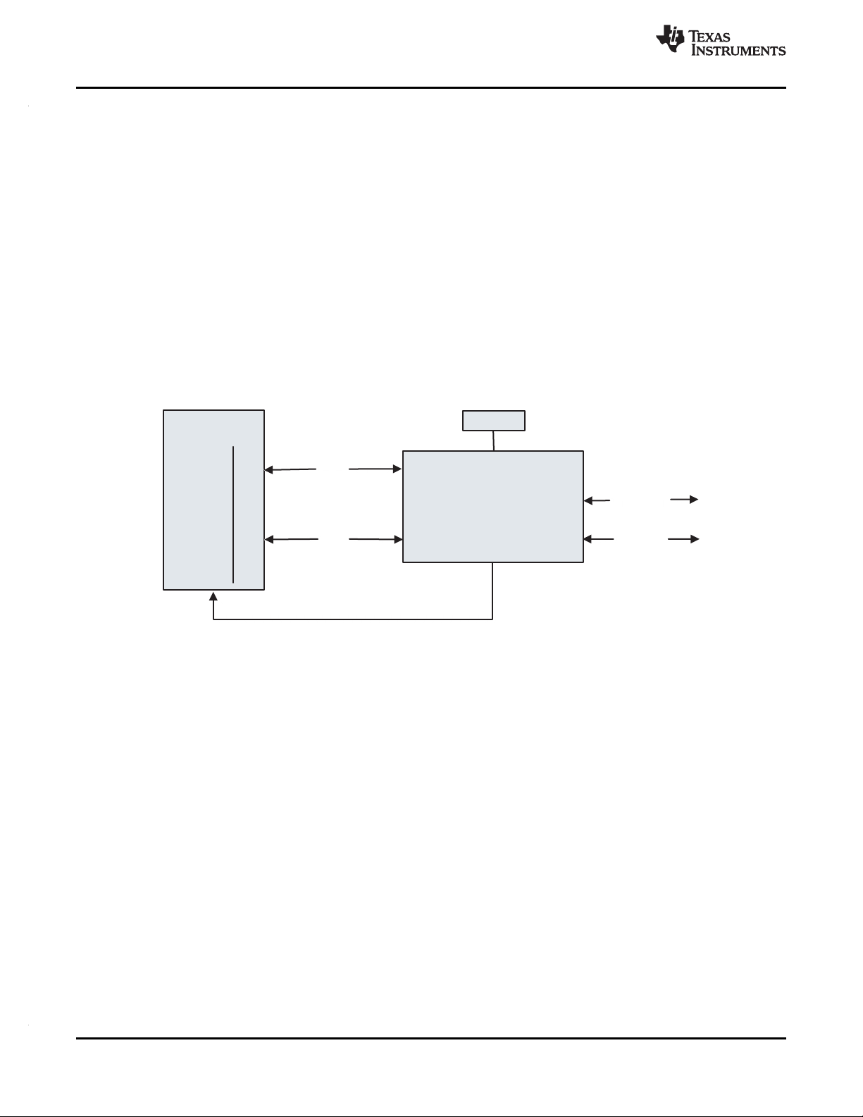
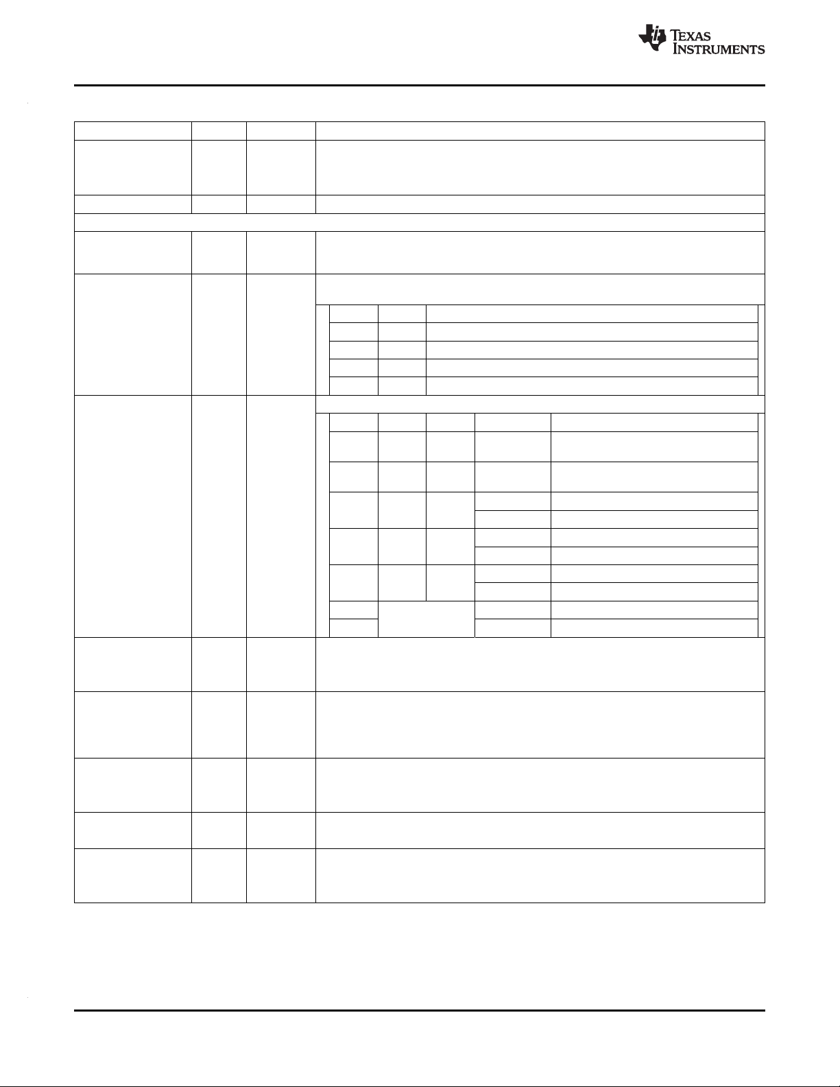
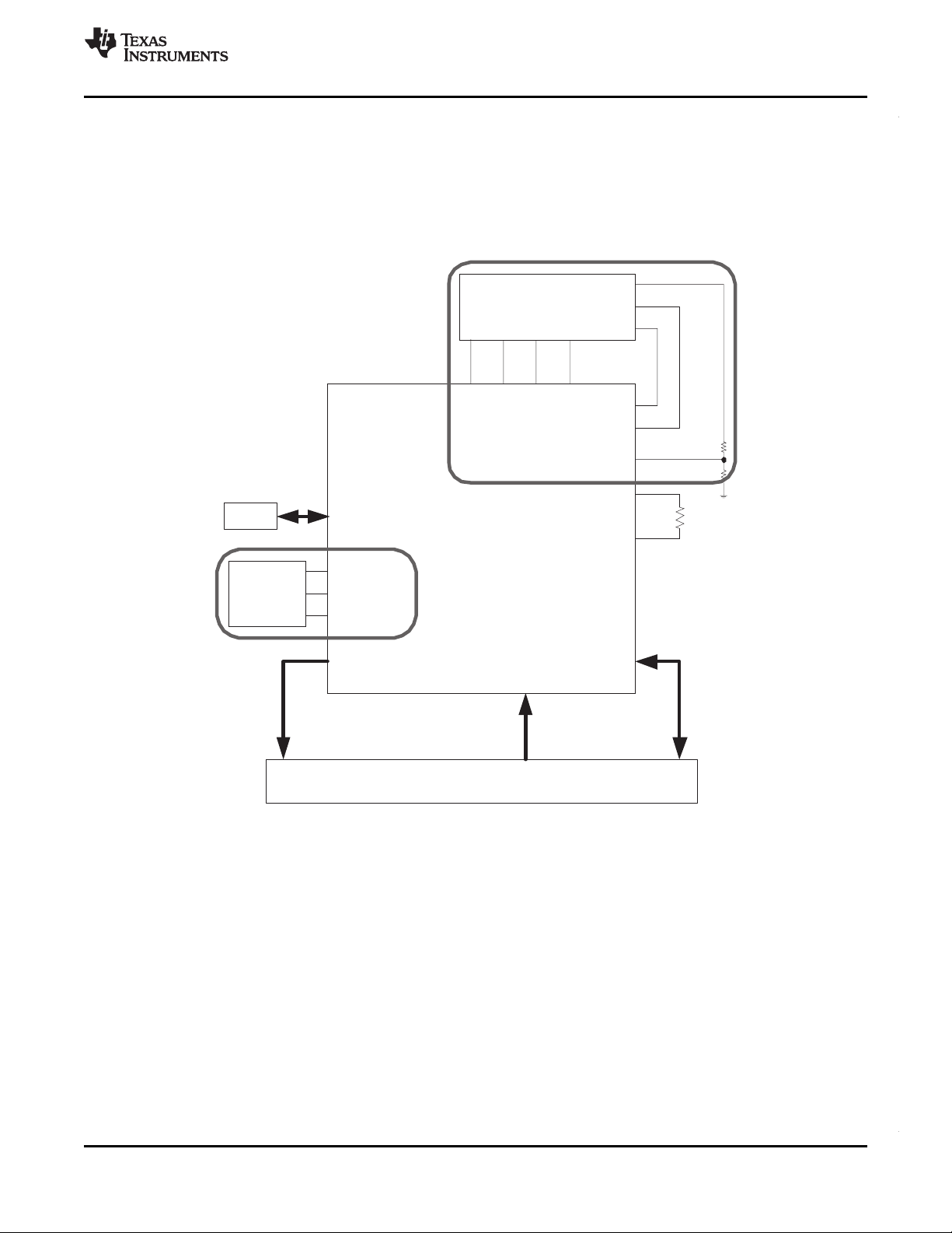
PRODUCTPREVIEW
PIPE
ULPI
MCU/CPU
Link Controller
(16 bit 250 MHz)
(8 bit 60 MHz)
Crystal
TUSB1310A
5.0 Gbps
SSTX P/N
SSRX P/N
DP/DM
CLKOUT
TUSB1310A
SLLSE32–NOVEMBER 2010
1.3 Introduction
The TUSB1310A is a single port, 5.0-Gbps USB 3.0 physical layer transceiver operating off of a single
reference clock provided by either a crystal or an external reference clock. The reference clock
frequencies are selectable from 20, 25, 30, and 40 MHz. The TUSB1310A provides the clock to the USB
controller. The use of a single reference clock allows the TUSB1310A to provide a cost effective USB 3.0
solution with few external components and a low implementation cost.
The USB controller interfaces to the TUSB1310A via a PIPE (SuperSpeed) and a ULPI (USB2.0)
interface. The 16-bit PIPE operates off of a 250-MHz interface clock. The ULPI supports 8-bit operations
with a 60-MHz interface clock.
USB 3.0 reduces active and idle power consumption with improved power management features. The
TUSB1310A low power states are controlled by the USB controller via the PIPE interface.
SuperSpeed USB uses existing USB software infrastructure by keeping the existing software interfaces
and software drivers intact. In addition, SuperSpeed USB retains backward compatibility with USB 2.0
based products by using the same form-factor Type-A connector and cables. Existing USB 2.0 devices will
work with new USB 3.0 hosts and new USB 3.0 devices with work with legacy USB 2.0 hosts.
www.ti.com
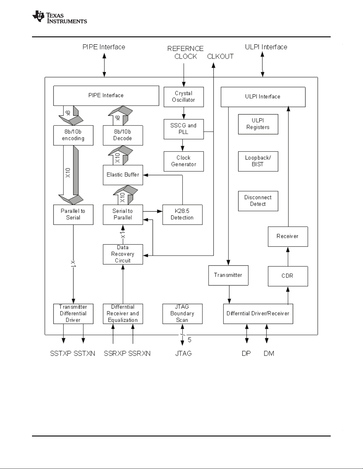
1.4 Functional Block Diagram
The USB physical layer handles the low level USB protocol and signaling. This includes data serialization
and deserialization, 8b/10b encoding, analog buffers, elastic buffers and receiver detection. It shifts the
clock domain of the data from the USB rate to one that is compatible with the link layer controller.
The SuperSpeed USB contains SSTXP/SSTXN and SSRXP/SSRXP differential pairs and uses the PIPE
to communicate with the link layer controller. The Non-SuperSpeed USB has a DP/DM differential pair and
communicates with the link layer controller via the ULPI. The TUSB1310A reference clock is connected to
an internal crystal oscillator, spread spectrum clock and PLL which provides clocks to all functional blocks
and to the CLKOUT pin for the link layer controller.
A JTAG interface is used for IEEE1149.1 and IEEE1149.6 boundary scan.
Figure 1-1. Typical Application
8 PRODUCT OVERVIEW Copyright © 2010, Texas Instruments Incorporated
Submit Documentation Feedback
Product Folder Link(s): TUSB1310A
PRODUCTPREVIEW
TUSB1310A
www.ti.com
SLLSE32–NOVEMBER 2010
Copyright © 2010, Texas Instruments Incorporated PRODUCT OVERVIEW 9
Figure 1-2. Functional Block Diagram
Submit Documentation Feedback
Product Folder Link(s): TUSB1310A
PRODUCTPREVIEW
TUSB1310A
SLLSE32–NOVEMBER 2010
2 PIN DESCRIPTIONS
TYPE DESCRIPTION
I Input
O Output
I/O Input/output
PD, PU Internal pull-down / pull-up
S Strapping pin
P Power Supply
G Ground
2.1 Configuration Pins
The configuration pins are not latched by RESETN.
Table 2-1. Configuration Pins
SIGNAL NAME TYPE PIN NO. MODE NAME DESCRIPTION
PHY_MODE1 I, PD H12 USB Must be set to 0. Operates as USB 3.0 transceiver.
PHY_MODE0 I, PU J12 USB Must be set to 1. Operates as USB 3.0 transceiver.
2.2 PIPE
www.ti.com
The TUSB1310A supports 16-bit SDR mode with a 250-MHz clock.
SIGNAL NAME TYPE BALL NO. DESCRIPTION
TX_CLK I K1
TX_DATA15 G2
TX_DATA14 H2
TX_DATA13 H1
TX_DATA12 J2
TX_DATA11 L3
TX_DATA10 L2
TX_DATA9 M2
TX_DATA8 M1
TX_DATA7 N1
TX_DATA6 P1
TX_DATA5 N2
TX_DATA4 P2
TX_DATA3 N3
TX_DATA2 P3
TX_DATA1 N4
TX_DATA0 P5
TX_DATAK1 G1
TX_DATAK0 J1
PCLK O A6 to this clock. This clock operates at 250 MHz. The rising edge of the clock is the reference
I The 16 bits represent 2 symbols of transmit data where TX_DATA7-0 is the first symbol to
I
Table 2-2. PIPE Signal Description
TX_DATA and TX_DATAK clock for source synchronous PIPE. This clock frequency is
the same as PCLK frequency. The rising edge of the clock is the reference for all signals.
Parallel USB SuperSpeed data input bus.
be transmitted, and TX_DATA15-8 is the second symbol.
Data/Control for the symbols of transmit data. TX_DATAK0 corresponds to the low-byte of
TX_DATA, TX_DATAK1 to the upper byte.
Parallel interface data clock. All data movement across the parallel PIPE is synchronous
for all signals.
10 PIN DESCRIPTIONS Copyright © 2010, Texas Instruments Incorporated
Submit Documentation Feedback
Product Folder Link(s): TUSB1310A
PRODUCTPREVIEW
TUSB1310A
www.ti.com
SIGNAL NAME TYPE BALL NO. DESCRIPTION
RX_DATA15 B9
RX_DATA14 A9
RX_DATA13 A8
RX_DATA12 B8
RX_DATA11 B5
RX_DATA10 B4
RX_DATA9 A4
RX_DATA8 B3
RX_DATA7 A3
RX_DATA6 A2
RX_DATA5 B1
RX_DATA4 C2
RX_DATA3 C1
RX_DATA2 D1
RX_DATA1 D2
RX_DATA0 E2
RX_DATAK1 B7 Data/Control for the symbols of receive data. RX_DATAK0 corresponds to the low-byte of
RX_DATAK0 A7
RX_VALID O F1 Active High. Indicates symbol lock and valid data on RX_DATA and RX_DATAK.
CONTROL AND STATUS SIGNALS
PHY_RESETN I, PU J3 Active Low. Resets the transmitter and receiver. This signal is asynchronous.
TX_DETRX_LPBK I, PD M6
TX_ELECIDLE I K3 Active High. Forces TX output to electrical idle depending on the power state.
RX_ELECIDLE F3
RX_STATUS2 C7
RX_STATUS1 C6 BIT 2 BIT 1 BIT 0 DESCRIPTION
RX_STATUS0 C5 0 0 0 Received data OK
O The 16 bits represent 2 symbols of receive data where RX_DATA7-0 is the first symbol
O RX_DATA, RX_DATAK1 to the upper byte. A value of zero indicates a data byte; a value
S, I/O, Active High. While de-asserted with the PHY in P0, P1, P2, or P3, indicates detection of
PD LFPS.
O
POWER_DOWN1 G3 Power up and down the transceiver power states.
POWER_DOWN0 H3 BIT 1 BIT 0 DESCRIPTION
I
SLLSE32–NOVEMBER 2010
Table 2-2. PIPE Signal Description (continued)
Parallel USB SuperSpeed data output bus.
received, and RX_DATA15-8 is the second.
of 1 indicates a control byte.
Active High. Used to tell the PHY to begin a receiver detection operation or to begin
loopback.
Encodes receiver status and error codes for the received data stream when receiving
data.
0 0 1 1 SKP ordered set added
0 1 0 1 SKP ordered set removed
0 1 1 Receiver detected
1 0 0 8B/10B decode error
1 0 1 Elastic buffer overflow
Elastic buffer underflow.
1 1 0 This error code is not used if the elasticity buffer is
operating in the nominal buffer empty mode.
1 1 1 Receive disparity error
0 0 P0, normal operation
0 1 P1, low recovery time latency, power saving state
1 0 P2, longer recovery time latency, low power state
1 1 P3, lowest power state
When transitioning from P3 to P0, the signaling is asynchronous.
Copyright © 2010, Texas Instruments Incorporated PIN DESCRIPTIONS 11
Submit Documentation Feedback
Product Folder Link(s): TUSB1310A
PRODUCTPREVIEW
TUSB1310A
SLLSE32–NOVEMBER 2010
SIGNAL NAME TYPE BALL NO. DESCRIPTION
PHY_STATUS E3
PWRPRESENT O H11 Indicates the presence of VBUS
CONFIGURATION PINS
TX_ONESZEROS I, PD M4 the transmitter to transmit an alternating sequence of 50 - 250 ones and 50 - 250 zeros –
TX_DEEMPH1 K11
TX_DEEMPH0 L11 BIT 1 BIT 0 DESCRIPTION
TX_MARGIN2 M11 Selects transmitter voltage levels
TX_MARGIN1 M10 BIT 2 BIT 1 BIT 0 TX_SWING DESCRIPTION
TX_MARGIN0 M9 0 0 0 0
S, I/O, management state transitions, rate change, and receiver detection. When this signal
PD transitions during entry and exit from P3 and PCLK is not running, then the signaling is
I, PD, PU
I, PD
TX_SWING I, PD M5 0 Full swing
RX_POLARITY I, PD C8
RX_TERMINATION I, PD D3 0 Terminations removed
RATE I, PU L6
ELAS_BUF_MODE I, PD C9 0 Nominal half full buffer mode
Table 2-2. PIPE Signal Description (continued)
Active High. Used to communicate completion of several PHY func-tions including power
asynchronous.
Active High. Used only when transmitting USB compliance pat-terns CP7 or CP8. Causes
regardless of the state of the TX_DATA interface.
Selects transmitter de-emphasis. When the MAC changes, the TUSB1310A starts to
transmit with the new setting within 128 ns.
0 0 -6 dB de-emphasis
0 1 -3.5 dB de-emphasis
1 0 No de-emphasis
1 1 Reserved
Normal operating range
800 mV - 1200 mV
0 0 0 1
0 0 1
0 1 0
0 1 1
1 0 200 mV - 400 mV
1 1 100 mV - 200 mV
Controls transmitter voltage swing level
1 Half swing
Active High. Tells PHY to do a polarity inversion on the received data. Inverted data show
up on RX_DATA15-0 within 20 PCLK clocks after RX_POLARITY is asserted.
0 PHY does no polarity inversion.
1 PHY does polarity inversion.
Controls presence of receiver terminations
1 Terminations present
Controls the link signaling rate
The RATE is always 1.
Selects elasticity buffer operating mode
1 Nominal empty buffer mode
Don't care
0 800 mV - 1200 mV
1 400 mV - 700 mV
0 700 mV - 900 mV
1 300 mV - 500 mV
0 400 mV - 600 mV
1 200 mV - 400 mV
Normal operating range
400 mV - 700 mV
www.ti.com
12 PIN DESCRIPTIONS Copyright © 2010, Texas Instruments Incorporated
Submit Documentation Feedback
Product Folder Link(s): TUSB1310A

PRODUCTPREVIEW
TUSB1310A
www.ti.com
2.3 ULPI
The ULPI (ultra low pin count interface) is a low pin count USB PHY to a link layer controller interface. The
ULPI consists of the interface and the ULPI registers. The TUSB1310A is always the master of the ULPI
bus.
Table 2-3. ULPI Signal Description
SIGNAL NAME TYPE BALL NO. DESCRIPTION
ULPI_CLK O P11
ULPI_DATA7 N6
ULPI_DATA6 P6
ULPI_DATA5 N7
ULPI_DATA4 P7
ULPI_DATA3 N8
ULPI_DATA2 P8
ULPI_DATA1 P9
ULPI_DATA0 N9
ULPI_DIR O M7 0 ULPI_DATA lines are inputs
ULPI_STP S, I, PU M8
ULPI_NXT O N11
S, I/O, PD
60-MHz interface clock. All ULPI signals are synchronous to ULPI_CLK. The ULPI_CLK is
always a 60-MHz output of the TUSB1310A. In low power mode, the ULPI_CLK is not driven.
Data bus. Driven to 00h by the Link when the ULPI bus is idle.
8-bit data timed on rising edge of ULPI_CLK
Controls the direction of the ULPI_DATA bus
1 ULPI_DATA lines are outputs
Active High. The Link must assert ULPI_STP to signal the end of a USB transmit packet or a
register write operation. The ULPI_STP signal must be asserted in the cycle after the last data
byte is presented on the bus. The ULPI_STP has an internal weak pull-up to safeguard
against false commands on the ULPI_DATA lines.
Active High. The PHY asserts ULPI_NXT to throttle all data types, except register read data
and the RX CMD. The PHY also asserts ULPI_NXT and ULPI_DIR simultaneously to indicate
USB receive activity, if ULPI_DIR was previously low. The PHY is not allowed to assert
ULPI_NXT during the first cycle of the TX CMD driven by the Link.
SLLSE32–NOVEMBER 2010
2.3.1 ULPI Modes
The TUSB1310A supports synchronous mode and low power mode. The default mode is synchronous
mode.
The synchronous mode is a normal operation mode. The ULPI_DATA are synchronous to ULPI_CLK. The
low power mode is used during power down and no ULPI_CLK. The TUSB1310A sets ULPI_DIR to output
and drives LineState signals and interrupts.
Table 2-4. ULPI Synchronous and Low Power Mode Functions
SYNCHRONOUS LOW POWER
ULPI_CLK(OUT)
ULPI_DATA7(I/O)
ULPI_DATA6(I/O)
ULPI_DATA5(I/O)
ULPI_DATA4(I/O)
ULPI_DATA3(I/O) ULPI_INT (OUT)
ULPI_DATA2(I/O)
ULPI_DATA1(I/O) ULPI_LINESTATE1(OUT)
ULPI_DATA0(I/O) ULPI_LINE_STATE0 (OUT)
ULPI_DIR(OUT)
ULPI_STP(IN)
ULPI_NXT(OUT)
Copyright © 2010, Texas Instruments Incorporated PIN DESCRIPTIONS 13
Submit Documentation Feedback
Product Folder Link(s): TUSB1310A
PRODUCTPREVIEW
TUSB1310A
SLLSE32–NOVEMBER 2010
2.4 Clocking
Table 2-5. Clock Signal Name Description
SIGNAL NAME TYPE BALL NO. DESCRIPTION
Crystal Input. This pin is the clock reference input for the TUSB1310A. The
XI I A12 TUSB1310A supports either a crystal unit, or a 1.8-V clock input. Frequencies
supported are 20, 25, 30, or 40 MHz.
XO O A11 Crystal output. If a 1.8-V clock input is connected to XI, XO must be left open.
CLKOUT O D10 OOBCLK is driven in U3 mode.
2.5 JTAG Interface
The JTAG Interface is used for board-level boundary scan. All digital IO support IEEE1149.1 boundary
scan and SuperSpeed differential pairs support IEEE1149.6 boundary scan.
Table 2-6. JTAG Signal Name Description
SIGNAL NAME TYPE BALL NO. DESCRIPTION
JTAG_TCK I, PU G11 JTAG test clock
JTAG_TMS I, PU D11 JTAG test mode select
JTAG_TDI I, PU E11 JTAG test data input
JTAG_TRSTN I, PD E12 JTAG test asynchronous reset. Active Low.
JTAG_TDO O F11 JTAG test data output
www.ti.com
2.6 Reset and Output Control Interface
SIGNAL NAME TYPE BALL NO. DESCRIPTION
RESETN I J11 Active Low. Resets the transmitter and receiver. This signal is asynchronous.
OUT_ENABLE I L10 0: Disable all driver outputs while IO powers are supplied, but internal control circuit
2.7 Strap Options
Strapping pins are latched by reset de-assertion in the TUSB1310A.
SIGNAL NAME TYPE BALL NO. DESCRIPTION
XTAL_DIS
(RX_ELECIDLE)
SSC_DIS
(TX_MARGIN0)
PIPE_16BIT
(PHY_STATUS)
S, I/O, PD F3 0 Crystal Input
S, I, PD M9 0 SSC enable
S, I/O, PD E3 0 16-bit PIPE SDR mode
Table 2-7. Reset and Output Control Signal Description
Active High. This can be connected to a 1.8-V power on reset signal on the PCB in
order to avoid static current and signal contention during power up.
powers are not present during power up.
1: Enable all driver outputs during normal operation.
Table 2-8. Strapping Options
Selects an input clock source
1 Clock Input
Spread spectrum clocking disable
1 SSC disable
Selects PIPE
Must be 0 at reset.
14 PIN DESCRIPTIONS Copyright © 2010, Texas Instruments Incorporated
Submit Documentation Feedback
Product Folder Link(s): TUSB1310A
PRODUCTPREVIEW
TUSB1310A
www.ti.com
Table 2-8. Strapping Options (continued)
SIGNAL NAME TYPE BALL NO. DESCRIPTION
Active High. Puts PIPE into isolate mode. When in the isolate mode, TUSB1310A does
not respond to packet data present at TX_DATA15-0, TXDATAK1-0 inputs and presents
ISO_START
(ULPI_DATA7)
ULPI_8BIT
(ULPI_DATA6)
REFCLKSEL1,
REFCLKSEL0 N7
(ULPI_DATA5, P7
ULPI_DATA4)
S, I/O, PD N6 When in the isolate mode, the TUSB1310A will continue to respond to ULPI. Once the
S, I/O, PD P6 0 8-bit ULPI SDR mode
S, I/O, PD 01 25 MHz on XI
a high imped-ance on the PCLK, RX_DATA15-0, RX_DATAK1-0, RX_VALID outputs.
isolate mode bit in ULPI register is cleared, the USB interfaces will start transmitting
packet data on TX_DATA15-0 and driving PCLK, RX_DATA15-0, RX_DATA1-0, and
RX_VALID.
Selects ULPI data bus bit width
Must be set to 0.
Select input reference clock frequency for on-chip oscillator
00 20 MHz on XI
10 30 MHz on XI
11 40 MHz on XI
2.8 USB Interfaces
Table 2-9. USB Interface Signal Name Descriptions
SIGNAL NAME TYPE BALL NO. DESCRIPTION
SSTXP H14
SSTXM J14
SSRXP E14
SSRXM F14
DP P14
DM P13
VBUS I N12
O USB SuperSpeed transmitter differential pair
I USB SuperSpeed receiver differential pair
I/O USB non-SuperSpeed differential pair
USB VBUS pin
Connected through an external voltage divider.
SLLSE32–NOVEMBER 2010
2.9 Special Connect
SIGNAL NAME TYPE BALL NO. DESCRIPTION
R1EXT O L14
R1EXTRTN I L13 R1 ground reference. This pin is not connected to board ground.
VDDA1P1 P M14 Needs a 1-µF bypass capacitor
RSVD I/O C14 Must be left open.
Copyright © 2010, Texas Instruments Incorporated PIN DESCRIPTIONS 15
Table 2-10. Special Connect Signal Descriptions
High precision external resistor used for calibration. The R1 value shall be 10 kΩ ±1%
accuracy.
D6
D5
C13
K4
J4
A14
Submit Documentation Feedback
Product Folder Link(s): TUSB1310A

PRODUCTPREVIEW
TUSB1310A
SLLSE32–NOVEMBER 2010
2.10 Power and Ground
SIGNAL NAME TYPE BALL NO. DESCRIPTION
VDDA3P3 P P12 Analog 3.3-V power supply
VDDA1P8 P A13 Analog 1.8-V power supply
VDDA1P1 P Analog 1.1-V power supply
VDD1P8 P Digital IO 1.8-V power supply
VDD1P1 P Digital 1.1-V power supply
VSSA G G12 Analog ground
VSSOSC G B12
www.ti.com
Table 2-11. Power/Ground Signal Descriptions
N14
C10
C12
K14
G13
G14
D14
C11
B2 C3
D4 D7
D8 D9
E4 F4
G4 H4
L5 L4
M3 L7
L8 L9
A5 A10
B6 B10
E1 F2
K2 L1
N5 P4
N10 P10
K13 D13
C4
B14 B13
J13 H13
F13 E13
K12 L12
D12
N13
M12
M13
Oscillator ground
If using a crystal, this should not be connected to PCB ground polane.
See Chapter 5 for guidelines.
If using an oscillator, this should be connected to PCB ground.
16 PIN DESCRIPTIONS Copyright © 2010, Texas Instruments Incorporated
Submit Documentation Feedback
Product Folder Link(s): TUSB1310A

PRODUCTPREVIEW
TUSB1310A
www.ti.com
Table 2-11. Power/Ground Signal Descriptions (continued)
SIGNAL NAME TYPE BALL NO. DESCRIPTION
F6 F7
F8 F9
G6 G7
G8 G9
VSS G J6 J7 Digital ground
H6 H7
H8 H9
J8 J9
B11 F12
SLLSE32–NOVEMBER 2010
Copyright © 2010, Texas Instruments Incorporated PIN DESCRIPTIONS 17
Submit Documentation Feedback
Product Folder Link(s): TUSB1310A
PRODUCTPREVIEW
TUSB1310A
SLLSE32–NOVEMBER 2010
3 FUNCTIONAL DESCRIPTION
3.1 Power On and Reset
The TUSB1310A has two hardware reset pins, a chip reset RESETN and a logic reset PHY_RESETN.
The RESETN is used only at Power On. The PHY_RESETN can be used as a functional reset. The ULPI
register also has a software reset.
Until all power sources are supplied, the OUT_ENABLE pin can control the output driver enable. After all
power sources are supplied, the chip reset RESETN and a ULPI soft reset will be asserted by the Link
Layer. The power up sequence is described in section 3.1.4
3.1.1 RESETN and PHY_RESETN – Hardware Reset
The RESETN sets all internal states to initial values. The Link Layer needs to hold the PHY in reset via
the RESETN until all power sources and the reference clock to the TUSB1310A are stable. All pins used
for strapping options must be set before RESETN de-assertion as they are latched by reset de-assertion.
All strapping option pins have internal pull-up or pull-down to set default values, but if any non-default
values are desired, they need to be controlled externally by the Link Layer Controller.
PIPE CONTROL PIN NAME STATE VALUE
TX_DETRX_LPBK Inactive 0
TX_ELECIDLE Active 1
TX_ONESZEROS Inactive 0
RX_POLARITY Inactive 0
POWER_DOWN U2 10b
TX_MARGIN2-0 Normal operating range 000b
TX_DEEMP -3.5 dB 1
RATE 5.0 Gbps 1
TX_SWING Full swing or half swing 0 or 1
RX_TERMINATION Appropriate state 0 or 1
www.ti.com
Table 3-1. Pin States in Chip Reset
3.1.2 ULPI Reset – Software Reset
After power-up, the Link Layer Controller must set the Reset bit in ULPI register. It resets the core but
does not reset the ULPI interface or the ULPI registers.
During the ULPI reset, the ULPI_DIR is de-asserted. After the reset, the ULPI_DIR is asserted again and
the TUSB1310A sends an RX CMD update to the Link Layer. During the reset, the link should ignore
signals on the ULPI_DATA7-0 and must not access the TUSB1310A.
3.1.3 OUT_ENABLE - Output Enable
Digital IO buffers use two power supplies, core VDD1P1 and IO VDD1P8. During power up,
OUT_ENABLE must be asserted low for proper operation.
3.1.4 Power Up Sequence
The power up sequence is shown in Figure 3-1.
18 FUNCTIONAL DESCRIPTION Copyright © 2010, Texas Instruments Incorporated
Submit Documentation Feedback
Product Folder Link(s): TUSB1310A

PRODUCTPREVIEW
Power Supplies
XI
RESETN
Internal latched
strapping pin states
Internal resetn/
PLL_EN/SUSPENDM
PCLK
ULPI_CLK
PHY_STATUS/
ULPI_DIR
Latched data
300 µs
TUSB1310A
www.ti.com
SLLSE32–NOVEMBER 2010
Figure 3-1. Power-Up Sequence
After proper power supply sequencing, the reference clock on XI starts to operate. On the RESETN
deassertion, REFCLKSEL1-0 is determined depending on the PHY_MODE pins, PLL is locked and the
valid ULPI_CLK and the valid PCLK are driven.
After all stable clocks are provided, the TUSB1310A allows the Link Layer Controller to access by
deasserting the ULPI_DIR. The Link Layer Controller sets the Reset bit in the ULPI register. At the PIPE
interface, the PHY_STATUS changes from high to low in order to indicate the TUSB1310A is in the power
state specified by the POWER_DOWN signal. After the PHY_STATUS change, the TUSB1310A is ready
for PIPE transactions.
3.2 Clocks
3.2.1 Clock Distribution
A source clock should be provided via XI/XO from an external crystal or from a square wave clock. The
USB3.0 PLL provides a clock to the PIPE which drives 250 MHz. The USB2.0 PLL provides a 60-MHz
clock to the ULPI.
3.2.2 Output Clock
The CLKOUT is used by the Link Layer Controller or the MAC in low power mode. A 120-MHz clock is
available on the CLKOUT pin only in the USB U3 power state.
3.3 Power Management
The SuperSpeed USB power state transition is controlled by the PIPE POWER_DOWN[1-0] and the
Non-SuperSpeed USB power state is transitioned by setting suspendM bit in the ULPI Function control
register via the ULPI or by asserting the ULPI_STP.
Copyright © 2010, Texas Instruments Incorporated FUNCTIONAL DESCRIPTION 19
Submit Documentation Feedback
Product Folder Link(s): TUSB1310A

PRODUCTPREVIEW
TUSB1310A
SLLSE32–NOVEMBER 2010
3.3.1 USB Power Management
The USB 3.0 specification improves power consumption by defining 4 power states, U0, U1, U2, and U3
while the PIPE specification defines P0, P1, P2 and P3. The POWER_DOWN pin states are mapped to
LTSSM states as described in Table 3-2. For all power state transitions, the Link Layer Controller must not
begin any operational sequences or further power state transitions until the TUSB1310A has indicated that
the internal state transition is completed.
PIPE
POWER USB POWER STATE PCLK PLL TRANSMITTING RECEIVING PHY_STATUS
STATE
P0 On On Active or Idle or LFPS Active or Idle A single cycle assertion
P1 U1 On On Idle or LFPS Idle A single cycle assertion
P2 On On Idle A single cycle assertion
P3 U3, SS.disabled an asynchronous Off LFPS or RxDetect Idle turned off and
U0, all other LTSSM
states
U2, RxDetect, Idle or LFPS or
SS.Inactive RxDetect
When the Link Layer Controller wants to transmit LFPS in P1, P2, or P3 state, it must de-assert
TX_ELECIDLE. The TUSB1310A generates valid LFPS until the TX_ELECIDLE is asserted. The Link
Layer Controller must assert TX_ELECIDLE before transitioning to P0.
When RX_ELECIDLE is de-asserted in P0, P1, P2, or P3, the TUSB1310A receiver monitors for LFPS
except during reset or when RX_TERMINATION is removed for electrical idle.
www.ti.com
Table 3-2. Power States
PHY_STATUS is
Off. The PIPE is in asserted before PCLK is
mode de-asserted when PCLK
is fully off.
When the TUSB1310A is in P0 and is actively transmitting; only RX_POLARITY can be asserted.
Table 3-3. PIPE Control Pin Matrix
POWER STATE TX_DETRX_LPBK TX_ELECIDLE DESCRIPTION
0 0 Transmitting data on TX_DATA.
P0
P1 Don’t care
P2 0 1 Idle
P3 Don’t care
0 1 Not transmitting and is in electrical idle
1 0 Goes into loopback mode
1 1 Transmits LFPS signaling
0 Transmits LFPS signaling
1 Not transmitting and is in electrical idle
Don’t care 0 Transmits LFPS signaling
1 1 Does a receiver detection operation
0 Transmits LFPS signaling
1 Does a receiver detection operation
20 FUNCTIONAL DESCRIPTION Copyright © 2010, Texas Instruments Incorporated
Submit Documentation Feedback
Product Folder Link(s): TUSB1310A

PRODUCTPREVIEW
TUSB1310A
www.ti.com
3.4 Receiver Status
The TUSB1310A has an elastic buffer for clock tolerance compensation, the Link Partner detection, and
some received data error detections. The receive data status from SSRXP/SSRXN differential pair
presents on RX_STATUS2-0. If an error occurs during a SKP ordered-set, the error signaling has
precedence. If more than one error occurs on a received byte, the errors have the priority below.
1. 8B/10B decode error
2. Elastic buffer overflow
3. Elastic buffer underflow (Can not occur in Nominal Empty buffer model)
4. Disparity error
3.4.1 Clock Tolerance Compensation
The receiver contains an elastic buffer used to compensate for differences in frequencies between bit
rates at the two ends of a Link. The elastic buffer must be capable of holding enough symbols to handle
worst case differences in frequency and worst case intervals between SKP ordered-sets. A SKP order-set
is a set of symbols transmitted as a group. The SKP ordered-sets allows the receiver to adjust the data
stream being received prevent the elastic buffer from either overflowing or under-flowing due to any clock
tolerance differences.
The TUSB1310A supports two models, Nominal Half Full buffer model and Nominal Empty buffer mode.
For the Nominal Half Full buffer model, the TUSB1310A monitors the receive data stream. When a Skip
ordered-set is received, the TUSB1310A adds or removes one SKP order set from each SKP to manage
its elastic buffer to keep the buffer as close to half full as possible. Only full SKP ordered sets are added
or removed. When a SKP order set is added, the TUSB1310A asserts an “Add SKP” code (001b) on the
RX_STATUS for one clock cycle. When a SKP order set is removed, the RX_STATUS is has a “Remove
SHP” code (010b).
SLLSE32–NOVEMBER 2010
For the Nominal Empty buffer model the TUSB1310A attempts to keep the elasticity buffer as close to
empty as possible. When no SKP ordered sets have been received, the TUSB1310A will be required to
insert SKP ordered sets into the received data stream.
RX_STATUS2-0 SKP ADDITION OR REMOVAL LENGTH
001b 1 SKP Ordered Set added
010b 1 SKP Ordered Set removed
3.4.2 Receiver Detection
TX_DETRX_LPBK starts a receiver detection operation to determine if there is a receiver at the other end
of the link. When the receiver detect sequence completes, the PHY_STATUS is asserted for one clock
and drives the RX_STATUS signals to the appropriate code. Once the TX_DETRX_LPBK signal is
asserted, the Link Layer Controller must leave the signal asserted until the PHY_STATUS pulse. When
receiver detection is performed in P3, the PHY_STATUS shows the appropriate receiver detect value until
the TX_DETRX_LPBK is de-asserted.
RX_STATUS2-0 DETECTED CONDITION LENGTH
000b Receiver not present
011b Receiver present
Table 3-4. RX_STATUS - SKP
One clock cycle
Table 3-5. RX_STATUS - Receiver Detection
One clock cycle
Copyright © 2010, Texas Instruments Incorporated FUNCTIONAL DESCRIPTION 21
Submit Documentation Feedback
Product Folder Link(s): TUSB1310A

PRODUCTPREVIEW
TUSB1310A
SLLSE32–NOVEMBER 2010
3.4.3 8b/10b Decode Errors
When the TUSB1310A detects an 8b/10b decode error, it will assert a SUB symbol in the data on the
RX_DATA where the bad byte occurred. In the same clock cycle that the SUB symbol is asserted on the
RX_DATA, the 8b/10b decode error code (100b) will be asserted on the RX_STATUS. 8b/10b Decoding
error has priority over all other receiver error codes and could mask out a disparity error occurring on the
other byte of data being clocked onto the RX_DATA with the SUB symbol.
RX_STATUS2-0 DETECTED ERROR LENGTH
100b 8B/10B Decode Error
3.4.4 Elastic Buffer Errors
When the elastic buffer overflows, data is lost during the reception of the data. The elastic buffer overflow
error code (101b) will be asserted on the RX_STATUS on the PCLK cycle the omitted data would have
been asserted. The data asserted on the RX_DATA is still valid data, the elastic buffer overflow error code
on the RX_STATUS just marks a discontinuity point in the data stream being received.
When the elastic buffer underflows, SUB symbols are inserted into the data stream on the RX_DATA to fill
the holes created by the gaps between valid data. For every PCLK cycle a SUB symbol is asserted on the
RX_DATA, an elastic buffer underflow error code (111b) is asserted on the RX_STATUS. In Nominal
Empty buffer mode, SKP ordered sets are transferred on RX_DATA and the underflow is not signaled.
www.ti.com
Table 3-6. 8b/10b Decode Errors
Clock cycles during the ef fected byte is transferred on
RX_DATA15-0
RX_STATUS2-0 DETECTED ERROR LENGTH
101b Elastic Buffer overflow Clock cycles the omitted data would have appeared
110b Elastic Buffer underflow.
3.4.5 Disparity Errors
When the TUSB1310A detects a disparity error, it will assert a disparity error code (111b) on the
RX_STATUS in the same PCLK cycle it asserts the erroneous data on the RX_DATA. The disparity code
does not discern which byte on the RX_DATA is the erroneous data.
RX_STATUS2-0 DETECTED ERROR LENGTH
111b Disparity Error
3.5 Loopback
The TUSB1310A begins an internal loopback operation from SSRXP/SSRXN differential pairs to
SSTXP/SSTXN differential pairs when the TX_DETRX_LPBK is asserted while holding TX_ELECIDLE
de-asserted. The TUSB1310A will stop transmitting data to the SSTXP/SSTXN signaling pair from the
TX_DATA and begin transmitting on the SSTXP/SSTXN signaling pair the data received at the
SSRXP/SSRXN signaling pair. This data is not routed through the 8b/10b coding/encoding paths. While in
the loopback operation, the received data is still sent to the RX_DATA. The data sent to the RX_DATA is
routed through the 10b/8b decoder.
Table 3-7. Elastic Buffer Errors
Clock cycles during the SUB symbol presence on
RX_DATA15-0
Table 3-8. Disparity Errors
Clock cycles during the ef fected byte is transferred
on RX_DATA15-0
The TX_DETRX_LPBK de-assertion will terminate the loopback operation and return to transmitting
TX_DATA over the SSTXP/SSTXN signaling pair. The TUSB1310A only transitions out of loopback on
detection of LFPS signaling by transitioning to P2 state and starting the LFPS handshake.
22 FUNCTIONAL DESCRIPTION Copyright © 2010, Texas Instruments Incorporated
Submit Documentation Feedback
Product Folder Link(s): TUSB1310A

PRODUCTPREVIEW
TUSB1310A
www.ti.com
3.6 Adaptive Equalizer
The adaptive equalizer dynamically adjusts the forward gain and peaking of the analog equalizer to
minimize the jitter at the cross over point of the eye diagram. This allows for greater jitter tolerance in the
RX.
SLLSE32–NOVEMBER 2010
Copyright © 2010, Texas Instruments Incorporated FUNCTIONAL DESCRIPTION 23
Submit Documentation Feedback
Product Folder Link(s): TUSB1310A

PRODUCTPREVIEW
TUSB1310A
SLLSE32–NOVEMBER 2010
4 REGISTERS
4.1 Register Definitions
ACCESS CODE EXPANDED NAME DESCRIPTION
rd Read Register can be read. Read-only if this is the only mode given.
wr Write Pattern on the data bus will be written over all bits of the register.
s Set Pattern on the data bus is OR’s with and written into the register.
c Clear
4.2 Register Map
The TUSB1310A contains the ULPI registers consisting of an immediate register set and an extended
register set.
REGISTER NAME
IMMEDIATE REGISTER SET
Vendor ID Low 00h
Vendor ID High 01h
Product ID Low 02h
Product ID High 03h
Function Control 04h-06h 04h 05h 06h
Interface Control 07h-09h 07h 08h 09h
Reserved 10h – 14h
Debug 15h
Scratch Register 16h-18h 16h 17h 18h
Reserved 19h-2Eh
www.ti.com
Table 4-1. Register Definitions
Pattern on the data bus is a mask. If a bit in the mask is set, then the
corresponding register bit will be set to zero (cleared).
Table 4-2. Register Map
ADDRESS (6 BITS)
rd wr set clr
4.2.1 Vendor ID and Product ID (00h-03h)
Table 4-3. Vendor ID and Product ID
ADDRESS BITS NAME ACCESS RESET DESCRIPTION
00h 7:00 Vendor ID Low rd 51h Lower byte of Vendor ID supplied by USB-IF
01h 7:00 Vendor ID High rd 04h Upper byte of Vendor ID supplied by USB-IF
02h 7:00 Product ID Low rd 10h Lower byte of Vendor ID supplied by Vendor
03h 7:00 Product ID High rd 13h Upper byte of Vendor ID supplied by Vendor
24 REGISTERS Copyright © 2010, Texas Instruments Incorporated
Submit Documentation Feedback
Product Folder Link(s): TUSB1310A

PRODUCTPREVIEW
TUSB1310A
www.ti.com
SLLSE32–NOVEMBER 2010
4.2.2 Function Control (04h-06h)
Address: 04h-06h (read), 04h (write), 05h (set), 06h (clear)
Table 4-4. Function Control
BITS NAME ACCESS RESET DESCRIPTION
Selects the required transceiver speed 00b : Enable HS
transceiver
1:0 XcvrSelect rd/wr/s/c 1h
2 TermSelect rd/wr/s/c 0 on XcvrSelect, OpMode, DpPulldown and DmPulldown. Since
4:3 OpMode rd/wr/s/c 00
5 Reset rd/wr/s/c 0 the ULPI_DIR, the PHY must re-assert the ULPI_DIR and
6 SuspendM rd/wr/s/c 1h The PHY must auto-matically set this bit to 1 when Low
7 Reserved rd 0 Reserved
01b: Enable FS transceiver
10b: Enable LS transceiver
11b: Enable FS transceiver for LS packets
(FS preamble is automatically pre-pended)
Controls the internal 1.5-kΩ pullup resister and 45-Ω HS
terminations. Control over bus resistors changes depending
low speed peripherals never support full speed or hi-speed,
providing the 1.5 kΩ on DM for low speed is optional.
Selects the required bit encoding style during transmit
00 : Normal operation
01: Non-driving
10: Disable bit-stuff and NRZI encoding
11: Do not automatically add SYNC and EOP when
transmitting. Must be used only for HS packets.
Active High transceiver reset. After the Link sets this bit, the
TUSB1310A must assert the ULPI_DIR and reset the ULPI.
When the reset is completed, the PHY de-asserts the
ULPI_DIR and automatically clears this bit. After de-asserting
send an RX CMD update on the Link Layer Controller. The
Link Layer Controller must wait for the ULPI_DIR to deassert before using the ULPI bus. Does not reset the ULPI or
ULPI register set.
Active low PHY suspend. Put the TUSB1310A into Low
Power Mode. The PHY can power down all blocks except the
full speed receiver, OTG com-parators, and the ULPI pins.
Power Mode is exited.
0: Low Power Mode
1: Powered
4.2.3 Interface Control (07h-09h)
Address: 07-09h (read), 07h (write), 08h (set), 09h (clear)
BITS NAME ACCESS RESET DESCRIPTION
0 Reserved rd 0b Reserved, only write a 0 to this bit.
1 Reserved rd 0b Reserved, only write a 0 to this bit.
2 Reserved rd 0h Reserved
3 ClockSuspendM rd/wr/s/c 0b when SuspendM = 0. By default, the clock will not be
6:4 Reserved rd 0h Reserved
Copyright © 2010, Texas Instruments Incorporated REGISTERS 25
Table 4-5. Interface Control
Active low clock suspend. Valid only in Serial Mode. Powers
down the internal clock circuitry only. Valid only when
SuspendM = 1. The TUSB1310A must ignore ClockSuspend
powered in Serial Mode.
0 : Clock will not be powered in Serial Mode
1 : Clock will be powered in Serial Mode
Submit Documentation Feedback
Product Folder Link(s): TUSB1310A

PRODUCTPREVIEW
TUSB1310A
SLLSE32–NOVEMBER 2010
Table 4-5. Interface Control (continued)
BITS NAME ACCESS RESET DESCRIPTION
Controls internal pullups and pulldowns on the ULPI_STP and
7 rd/wr/s/c 0 Controller tri-states the signals.
Interface
Protect Disable
the ULPI_DATA for protecting the ULPI when the Link Layer
0 Enables the pullup and pulldown
1 Disables the pullup and pulldown
4.2.4 Debug (15h)
Address: 15h (read-only)
Table 4-6. Debug
BITS NAME ACCESS RESET DESCRIPTION
0 LineState0 rd 0 Contains the current value of LineState0
1 LineState1 rd 0 Contains the current value of LineState1
7:2 Reserved rd 0 Reserved
4.2.5 Scratch Register (16-18h)
Address: 16-18h (read), 16h (write), 17h (set), 18h (clear)
Table 4-7. Scratch Register
www.ti.com
BITS NAME ACCESS RESET DESCRIPTION
7:0 Scratch rd/wr/s/c 00 write, set, and clear this register and the TUSB1310A
Empty register byte for testing purposes. Software can read,
functionality will not be affected.
26 REGISTERS Copyright © 2010, Texas Instruments Incorporated
Submit Documentation Feedback
Product Folder Link(s): TUSB1310A
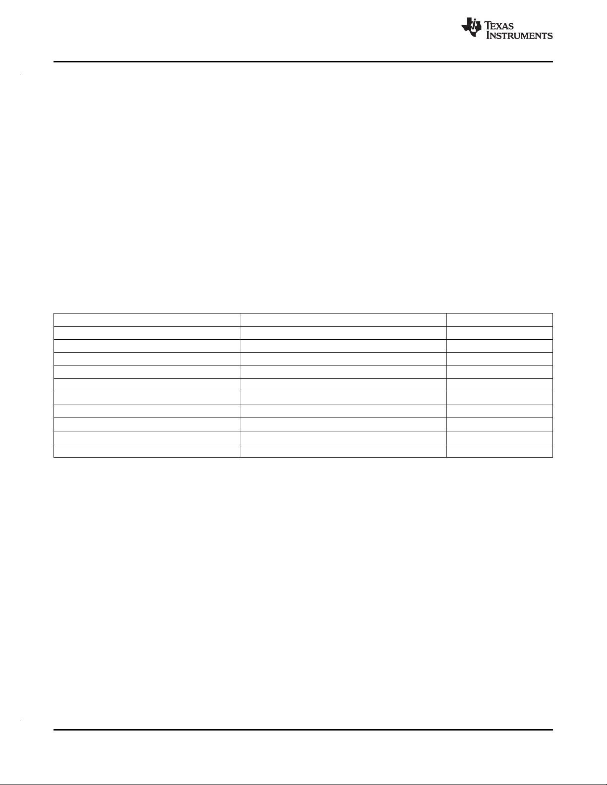
PRODUCTPREVIEW
R1EXT
R1EXTRTN
10K ± 1%W
SSRXP
VBUS
SSRXN
SSTXP
SSTXN
DP
DM
USB Connector
XI
VSSOSC
XO
Crystal
Connection
ULPIPIPE RX
PIPE TX
Link Controller
JTAGJTAG
10K ± 1%W
90.9K ± 1%W
TUSB1310A
www.ti.com
5 DESIGN GUIDELINES
5.1 Chip Connection on PCB
Components should be placed close to the TUSB1310A to reduce the trace length of the interface
between the components and the TUSB1310A. If external capacitors can not accommodate a close
placement, shielding to ground is recommended.
SLLSE32–NOVEMBER 2010
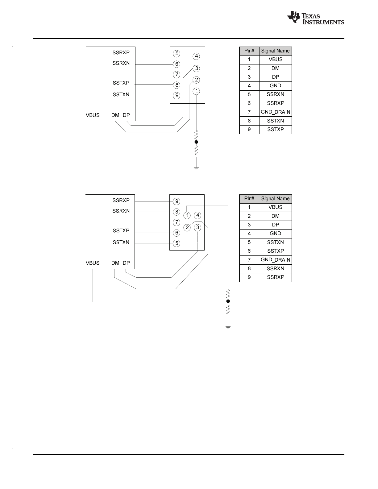
5.1.1 USB Connector Pins Connection
Differential pair signals, DP/DM, SSTXP/SSTXN, SSRXP/SSRXN, should be kept as short as possible.
The differential pair traces should be trace-length matched and parallelism should be maintained. They
also need to minimize vias and corners and should avoid crossing plane splits and stubs.
Figure 5-2 and Figure 5-3 are for visual reference only.
Copyright © 2010, Texas Instruments Incorporated DESIGN GUIDELINES 27
Figure 5-1. Analog Pin Connections
Submit Documentation Feedback
Product Folder Link(s): TUSB1310A
PRODUCTPREVIEW
90.9 k ±1%W
10 k ±1%W
90.9 k ±1%W
10 k ±1%W
TUSB1310A
SLLSE32–NOVEMBER 2010
www.ti.com
Figure 5-2. USB Standard-A Connector Pin Connection
5.1.2 Clock Connections
The TUSB1310A supports an external oscillator source or a crystal unit. If a clock is provided to XI instead
of a crystal, XO is left open. Otherwise, if a crystal is used, the connection needs to follow the guidelines
below.
Since XI and XO are coupled to other leads and supplies on the PCB, it is important to keep them as short
as possible and away from any switching leads. It is also recommended to minimize the capacitance
between XI and XO. This can be accomplished by connecting the VSSOSC lead to the two external
capacitors CL1 and CL2 and shielding them with the clean ground lines. The VSSOSC should not be
connected to PCB ground.
Figure 5-3. USB Standard-B Connector Pin Connection
28 DESIGN GUIDELINES Copyright © 2010, Texas Instruments Incorporated
Submit Documentation Feedback
Product Folder Link(s): TUSB1310A

PRODUCTPREVIEW
VDDO1P1
XI
VSSOSC
XO
VDDO1P8
VSSO
CL1
Crystal
VDD1P8
CL2
VDD1P1
·
·
·
TUSB1310A
www.ti.com
Load capacitance (Cload) of the crystal varying with the crystal vendors is the total capacitance value of
the entire oscillation circuit system as seen from the crystal. It includes two external capacitors CL1 and
CL2 in Figure 5-4. The trace length between the decoupling capacitors and the corresponding power pins
on the TUSB1310A needs to be minimized. It is also recommended that the trace length from the
capacitor pad to the power or ground plane be minimized.
SLLSE32–NOVEMBER 2010
5.2 Clock Source Requirements
5.2.1 Clock Source Selection Guide
Reference clock jitter is an important parameter. Jitter on the reference clock will degrade both the
transmit eye and receiver jitter tolerance no matter how clean the rest of the PLL is, thereby impairing
system performance. Additionally, a particularly jittery reference clock may interfere with PLL lock
detection mechanism, forcing the Lock Detector to issue an Unlock signal. A good quality, low jitter
reference clock is required to achieve compliance with supported USB3.0 standards. For example,
USB3.0 specification requires the random jitter (RJ) component of either RX or TX to be 2.42 ps (random
phase jitter calculated after applying jitter transfer function - JTF). As the PLL typically has a number of
additional jitter components, the Reference Clock jitter must be considerably below the overall jitter
budget.
5.2.2 Oscillator
If an external clock source is used, XI should be tied to the clock source and XO should be left floating.
PARAMETER MIN TYP MAX UNITS CONDITION
Frequency tolerance ±50 ppm Operational temperature
Frequency stability ±50 ppm 1 year aging
Rise/Fall time 6 nsec 20% - 80%
Reference clock R
with JTF (1 sigma)
J
(1)(2)
Figure 5-4. Typical Crystal Connections
Table 5-1. Oscillator Specification
0.8 psec
(1) Sigma value assuming Gaussian distribution
(2) After application of JTF
Copyright © 2010, Texas Instruments Incorporated DESIGN GUIDELINES 29
Submit Documentation Feedback
Product Folder Link(s): TUSB1310A

PRODUCTPREVIEW
TUSB1310A
SLLSE32–NOVEMBER 2010
Table 5-1. Oscillator Specification (continued)
PARAMETER MIN TYP MAX UNITS CONDITION
Reference clock T
with JTF (total p-p)
Reference clock jitter
(absolute p-p)
(3) Calculated as 14.1 x RJ+ D
(4) Absolute phase jitter (p-p)
(4)
J
(2)(3)
25 psec
50 psec
J
5.2.3 Crystal
Either a 20-MHz, 25-MHz, 30-MHz, or 40-MHz crystal can be selected. A parallel, 20-pF load crystal
should be used if a crystal source is used.
Table 5-2. Crystal Specification
PARAMETER MIN TYP MAX UNITS CONDITION
Frequency tolerance ±50 ppm Operational temperature
Frequency stability ±50 ppm 1 year aging
Load capacitance 12 20 24 pF
www.ti.com
30 DESIGN GUIDELINES Copyright © 2010, Texas Instruments Incorporated
Submit Documentation Feedback
Product Folder Link(s): TUSB1310A

PRODUCTPREVIEW
TUSB1310A
www.ti.com
SLLSE32–NOVEMBER 2010
6 ELECTRICAL SPECIFICATIONS
6.1 ABSOLUTE MAXIMUM RATINGS
over operating free-air temperature range (unless otherwise noted)
VALUE UNIT
VDD1P1 steady-state supply voltage –0.3 to 1.4 V
VDD1P8 steady-state supply voltage –0.3 to 2.45 V
VDDA1P1 steady-state supply voltage –0.3 to 1.4 V
VDDA1P8 steady-state supply voltage –0.3 to 2.45 V
VDDA3P3 steady-state supply voltage –0.3 to 3.8 V
6.2 RECOMMENDED OPERATING CONDITIONS
over operating free-air temperature range (unless otherwise noted)
MIN NOM MAX UNIT
VDDA3P3 Analog 3.3 supply voltage 2.97 3.3 3.63 V
VDDA1P8 Analog 1.8 supply voltage 1.71 1.8 1.98 V
VDDA1P1 Analog 1.1 supply voltage 1.045 1.1 1.155 V
VDD1P8 Digital IO 1.8 supply voltage 1.62 1.8 1.98 V
VDD1P1 Digital 1.1 supply voltage 1.045 1.1 1.155 V
VBUS Voltage at VBUS PAD 0 1.155 V
T
A
T
J
Operating free-air temperature range -40 85 °C
Operating junction temperature range -40 105 °C
ESD V
Human body model (HBM) 2000
Charged device model (CDM) 500
6.3 DC CHARACTERISTICS for 1.8-V DIGITAL IO
over operating free-air temperature range (unless otherwise noted)
PARAMETER TEST CONDITIONS MIN TYP MAX UNIT
V
IH
V
IL
V
OH
High-level input voltage 0.65 V
Low-level input voltage 0.35 V
V
OL
V
hys
I
I
Input hysteresis 100 270 mV
IO= -2 mA,
V
= 1.62 V to 1.98 V,
DDS
driver enabled, pullup or
pulldown disabled
IO= -2 mA,
V
= 1.4 V to 1.6 V,
DDS
driver enabled, pullup or
pulldown disabled
IO= 2 mA,
V
= 1.62 V to 1.98 V,
DDS
driver enabled, pullup or
pulldown disabled
IO= 2 mA,
V
= 1.4 V to 1.6 V,
DDS
driver enabled, pullup or
pulldown disabled
Any receiver, including those
with a pullup or pulldown. The
pullup or pulldown must be
disabled.
V
DDS
0.75 V
DDS
- 0.45
DDS
0.25 V
DDS
0.45
DDS
±1 µA
V
V
V
V
Copyright © 2010, Texas Instruments Incorporated ELECTRICAL SPECIFICATIONS 31
Submit Documentation Feedback
Product Folder Link(s): TUSB1310A

PRODUCTPREVIEW
TUSB1310A
SLLSE32–NOVEMBER 2010
DC CHARACTERISTICS for 1.8-V DIGITAL IO (continued)
over operating free-air temperature range (unless otherwise noted)
PARAMETER TEST CONDITIONS MIN TYP MAX UNIT
I
I(PUon)
I
OZ
I
Z
V
TX_DIFF_SS
R
TX_DIFF_DC
V
TX_RCV_DET
C
AC_COUPLING
RRX_DC 18 30 Ω
RRX_DIFF_DC DC differential impedance 72 120 Ω
VRX_LFPS_DET LFPS detect threshold 100 300 mV
VCM_AC_LFPS 100 mV
VCM_LFPS_active 10 mV
VTX_DIFF_PP_LFPS 800 1200 mV
(1) IZis the total leakage current through the PAD connection of a driver/receiver combination that may include a pullup or pulldown. The
driver output is disabled and the pullup or pulldown is inhibited.
See
SSTXP/SSTXN differential
p-p TX voltage swing
DC differential impedance 72 120 Ω
The amount of voltage
change allowed during 0.6 V
receiver detection
AC coupling capacitor 75 200 nF
Receiver DC common
mode impedance
www.ti.com
Receiver/pullup only, pullup
enabled (not inhibited), -47 to -169
V
= 0 V
PAD
Receiver/pullup only, pullup
enabled (not inhibited)
Driver only, driver disabled ±20 µA
(1)
0.8 1.2 V
–100
±20 µA
µA
6.4 DEVICE POWER CONSUMPTION
(1)
over operating free-air temperature range (unless otherwise noted)
PARAMETER MIN TYP MAX UNIT
VDDA3P3 power consumption 13 mW
VDDA1P8 power consumption 77 mW
VDDA1P1 power consumption 118 mW
VDD1P1 power consumption 98 mW
VDD1P8 power consumption 128 mW
(1) Power consumption condition is transmitting and/or receiving (in U0) at 25°C and nominal voltages.
6.5 AC Characteristics
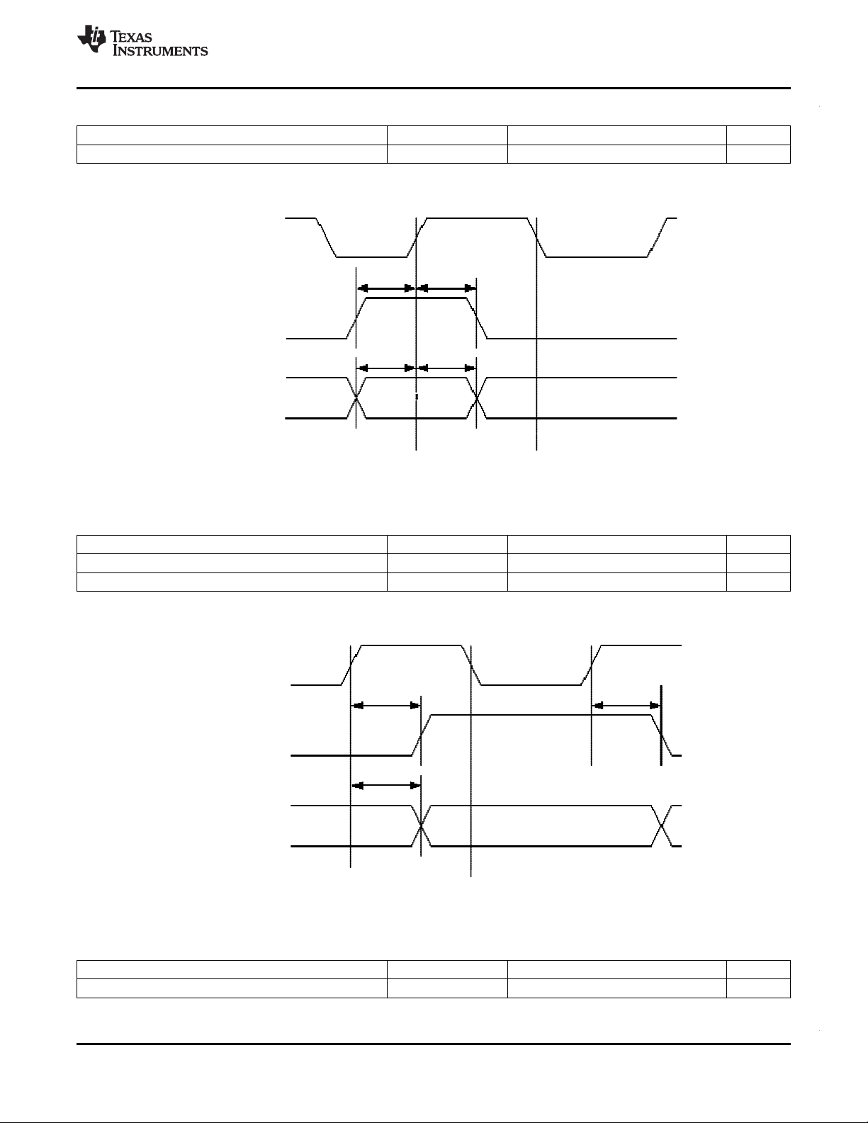
6.5.1 Power Up and Reset Timing
The TUSB1310A does not drive signals on any strapping pins before they are latched internally.
32 ELECTRICAL SPECIFICATIONS Copyright © 2010, Texas Instruments Incorporated
Submit Documentation Feedback
Product Folder Link(s): TUSB1310A

PRODUCTPREVIEW
VDD1P1
VDD1P8 and
Analog Power Supplies
OUT_ENABLE
XI
RESETN
Latch-In of Hardware
Strapping Pins
ULPI_DIR
Tcfgin1
Drive Output
Strapping pins
Tcfgin2
TUSB1310A
www.ti.com
SLLSE32–NOVEMBER 2010
Figure 6-1. Power Up and Reset Timing
DESCRIPTION SYMBOL MIN TYP MAX UNITS
Hardware configuration latch-in time from RESETN Tcfgin1 0 ns
Time from RESETN to driver outputs on strapping pins Tcfgin2 0 ns
RESETN pulse width 1 µs
RESETN to PHY_STATUS de-assertion 300 µs
6.5.2 PIPE Transmit
TX_CLK period Tcyc2 4 ns
TX_CLK duty cycle Tdty2 50 %
Data setup to TX_CLK rise and TX_CLK fall
Data hold to TX_CLK rise and TX_CLK fall
(1) This includes TX_DATA15-0, TX_DATAK1-0, TX_ONESZEROS, RATE, TX_DEEMPTH, TX_DETRX_LPBK, TX_ELECIDLE,
TX_MARGIN, TX_SWING, RX_POLARITY, POWER_DOWN1-0.
DESCRIPTION SYMBOL MIN TYP MAX UNITS
Table 6-1. Power Up and Reset Timing
Figure 6-2. PIPE Transmit Timing
Table 6-2. PIPE Transmit Timing
(1)
(1)
Tsu2 1 ns
Thd2 0 ns
Copyright © 2010, Texas Instruments Incorporated ELECTRICAL SPECIFICATIONS 33
Submit Documentation Feedback
Product Folder Link(s): TUSB1310A

PRODUCTPREVIEW
PCLK
RX_DATA15-0
RX_DATAK1-0
RX_VALID
RX_STATUS2-0
PHY_STATUS
Valid Data
Tcyc3
Tdly3
TUSB1310A
SLLSE32–NOVEMBER 2010
www.ti.com
6.5.3 PIPE Receive
Figure 6-3. PIPE Receive Timing
Table 6-3. PIPE Receive Timing
SYMBOL DESCRIPTION MIN TYP MAX UNIT
Tcyc3 PCLK Period 4 ns
Tdty3 PCLK Duty Cycle 50 %
Tdly3 1 2 ns
(1) Output Load max = 10 pF, min = 5 pF
(2) Timing is relative to the 50% transition point, not VIH/VIL.
PCLK rise and fall to RX_DATA15-0, RX_DATAK1-0, RX_VALID,
RX_STATUS2-0, PHY_STATUS Delay
(1)(2)
6.5.4 ULPI Parameters
DESCRIPTION NOTES HS FS LS UNIT
RX CMD delay 2-4 2-4 2-4 clocks
TX start delay 1-2 1-10 1-10 clocks
TX end delay PHY pipeline delays 2-5 clocks
RX start delay 3-8 clocks
RX end delay 3-8 17-18 122-123 clocks
Transmit-Transmit (host only) 15-24 7-18 77-247 clocks
Receive-Transmit (host or peripheral) 1-14 7-18 77-247 clocks
6.5.5 ULPI Clock
DESCRIPTION SYMBOL MIN TYP MAX UNITS
Frequency (first transition) ±10% Fstart_8bit 54 60 66 MHz
Frequency (steady state) ±500 ppm Fsteady 59.97 60 60.03 MHz
Duty cycle (first transition) ±10% Dstart_8bit 40 50 60 %
Duty cycle (steady state) ±500 ppm Dsteady 49.97 5 50 50.02 5 %
Time to reach steady state frequency and duty cycle after
first transition
Clock startup time after deassertion of SuspemdM –
Peripheral
Clock startup time after deassertion of SuspemdM – Hold Tstart_host ms
PHY preparation time after first transition of input clock Tprep µs
Jitter Tjitter ps
34 ELECTRICAL SPECIFICATIONS Copyright © 2010, Texas Instruments Incorporated
Table 6-4. ULPI Parameters
Link decision times
Table 6-5. ULPI Clock Parameters
Tsteady 1.4 ms
Tstart_dev 5.6 ms
Submit Documentation Feedback
Product Folder Link(s): TUSB1310A
PRODUCTPREVIEW
ULPI_CLK
ULPI_STP
ULPI_DATA7-0 In
(8-bit)
Tsc8
Thc8
Tsd8 Thd8
Tsdd8 Thdd8
Valid Data
Tsdd8
Thdd8
ULPI_CLK
ULPI_DIR
ULPI_NXT
ULPI_DATA7-0 Out
(8-bit)
Tdc9
Tdd9
Tddd9
Tdc9
Valid Data
Tddd9
TUSB1310A
www.ti.com
SLLSE32–NOVEMBER 2010
Table 6-5. ULPI Clock Parameters (continued)
DESCRIPTION SYMBOL MIN TYP MAX UNITS
Rise and fall time Trise/Tfall ns
6.5.6 ULPI Transmit
Figure 6-4. ULPI Transmit Timing
DESCRIPTION SYMBOL MIN TYP MAX UNITS
ULPI_STP setup time Tsc8, Tsd8 6 ns
ULPI_STP hold time Thc8, Thd8 0 ns
6.5.7 ULPI Receive Timing
ULPI_DIR/ULPI_NXT/ULPI_DATA7-0
(1) Output Load max = 10 pF, min = 5 pF
Copyright © 2010, Texas Instruments Incorporated ELECTRICAL SPECIFICATIONS 35
DESCRIPTION SYMBOL MIN TYP MAX UNITS
Table 6-6. ULPI Transmit Timing
Figure 6-5. ULPI Receive Timing
Table 6-7. ULPI Receive Timing
(1)
Submit Documentation Feedback
Product Folder Link(s): TUSB1310A
Tdc9, Tdd9 9 ns

PRODUCTPREVIEW
TUSB1310A
SLLSE32–NOVEMBER 2010
6.5.8 Power State Transition Time
The P1 to P0 transition time is the amount of time for the TUSB1310A to return to P0 state, after having
been in the P1 state. This time is measured from when the MAC sets the POWER_DOWN signals to P0
until the TUSB1310A asserts PHY_STATUS. The TUSB1310A asserts PHY_STATUS when it is ready to
begin data transmission and reception.
The P2 to P0 transition time is the amount of time for the TUSB1310A to return to the P0 state, after
having been in the P2 state. This time is measured from when the MAC sets the POWER_DOWN signals
to P0 until the TUSB1310A asserts PHY_STATUS. The TUSB1310A asserts PHY_STATUS when it is
ready to begin data transmission and reception.
The P3 to P0 transition time is the amount of time for the TUSB1310A to go to P0 state, after having been
in the P3 state. Time is measured from when the MAC sets the POWER_DOWN signals to P0 until the
TUSB1310A deasserts PHY_STATUS. The TUSB1310A asserts PHY_STATUS when it is ready to begin
data transmission and reception.
www.ti.com
36 ELECTRICAL SPECIFICATIONS Copyright © 2010, Texas Instruments Incorporated
Submit Documentation Feedback
Product Folder Link(s): TUSB1310A

PACKAGE OPTION ADDENDUM
www.ti.com
25-Nov-2010
PACKAGING INFORMATION
Orderable Device
TUSB1310AZAY PREVIEW NFBGA ZAY 175 160 TBD Call TI Call TI Samples Not Available
TUSB1310AZAYR PREVIEW NFBGA ZAY 175 1000 TBD Call TI Call TI Samples Not Available
(1)
The marketing status values are defined as follows:
ACTIVE: Product device recommended for new designs.
LIFEBUY: TI has announced that the device will be discontinued, and a lifetime-buy period is in effect.
NRND: Not recommended for new designs. Device is in production to support existing customers, but TI does not recommend using this part in a new design.
PREVIEW: Device has been announced but is not in production. Samples may or may not be available.
OBSOLETE: TI has discontinued the production of the device.
Status
(1)
Package Type Package
Drawing
Pins Package Qty
Eco Plan
(2)
Lead/
Ball Finish
MSL Peak Temp
(3)
Samples
(Requires Login)
(2)
Eco Plan - The planned eco-friendly classification: Pb-Free (RoHS), Pb-Free (RoHS Exempt), or Green (RoHS & no Sb/Br) - please check http://www.ti.com/productcontent for the latest availability
information and additional product content details.
TBD: The Pb-Free/Green conversion plan has not been defined.
Pb-Free (RoHS): TI's terms "Lead-Free" or "Pb-Free" mean semiconductor products that are compatible with the current RoHS requirements for all 6 substances, including the requirement that
lead not exceed 0.1% by weight in homogeneous materials. Where designed to be soldered at high temperatures, TI Pb-Free products are suitable for use in specified lead-free processes.
Pb-Free (RoHS Exempt): This component has a RoHS exemption for either 1) lead-based flip-chip solder bumps used between the die and package, or 2) lead-based die adhesive used between
the die and leadframe. The component is otherwise considered Pb-Free (RoHS compatible) as defined above.
Green (RoHS & no Sb/Br): TI defines "Green" to mean Pb-Free (RoHS compatible), and free of Bromine (Br) and Antimony (Sb) based flame retardants (Br or Sb do not exceed 0.1% by weight
in homogeneous material)
(3)
MSL, Peak Temp. -- The Moisture Sensitivity Level rating according to the JEDEC industry standard classifications, and peak solder temperature.
Important Information and Disclaimer:The information provided on this page represents TI's knowledge and belief as of the date that it is provided. TI bases its knowledge and belief on information
provided by third parties, and makes no representation or warranty as to the accuracy of such information. Efforts are underway to better integrate information from third parties. TI has taken and
continues to take reasonable steps to provide representative and accurate information but may not have conducted destructive testing or chemical analysis on incoming materials and chemicals.
TI and TI suppliers consider certain information to be proprietary, and thus CAS numbers and other limited information may not be available for release.
In no event shall TI's liability arising out of such information exceed the total purchase price of the TI part(s) at issue in this document sold by TI to Customer on an annual basis.
Addendum-Page 1


IMPORTANT NOTICE
Texas Instruments Incorporated and its subsidiaries (TI) reserve the right to make corrections, modifications, enhancements, improvements,
and other changes to its products and services at any time and to discontinue any product or service without notice. Customers should
obtain the latest relevant information before placing orders and should verify that such information is current and complete. All products are
sold subject to TI’s terms and conditions of sale supplied at the time of order acknowledgment.
TI warrants performance of its hardware products to the specifications applicable at the time of sale in accordance with TI’s standard
warranty. Testing and other quality control techniques are used to the extent TI deems necessary to support this warranty. Except where
mandated by government requirements, testing of all parameters of each product is not necessarily performed.
TI assumes no liability for applications assistance or customer product design. Customers are responsible for their products and
applications using TI components. To minimize the risks associated with customer products and applications, customers should provide
adequate design and operating safeguards.
TI does not warrant or represent that any license, either express or implied, is granted under any TI patent right, copyright, mask work right,
or other TI intellectual property right relating to any combination, machine, or process in which TI products or services are used. Information
published by TI regarding third-party products or services does not constitute a license from TI to use such products or services or a
warranty or endorsement thereof. Use of such information may require a license from a third party under the patents or other intellectual
property of the third party, or a license from TI under the patents or other intellectual property of TI.
Reproduction of TI information in TI data books or data sheets is permissible only if reproduction is without alteration and is accompanied
by all associated warranties, conditions, limitations, and notices. Reproduction of this information with alteration is an unfair and deceptive
business practice. TI is not responsible or liable for such altered documentation. Information of third parties may be subject to additional
restrictions.
Resale of TI products or services with statements different from or beyond the parameters stated by TI for that product or service voids all
express and any implied warranties for the associated TI product or service and is an unfair and deceptive business practice. TI is not
responsible or liable for any such statements.
TI products are not authorized for use in safety-critical applications (such as life support) where a failure of the TI product would reasonably
be expected to cause severe personal injury or death, unless officers of the parties have executed an agreement specifically governing
such use. Buyers represent that they have all necessary expertise in the safety and regulatory ramifications of their applications, and
acknowledge and agree that they are solely responsible for all legal, regulatory and safety-related requirements concerning their products
and any use of TI products in such safety-critical applications, notwithstanding any applications-related information or support that may be
provided by TI. Further, Buyers must fully indemnify TI and its representatives against any damages arising out of the use of TI products in
such safety-critical applications.
TI products are neither designed nor intended for use in military/aerospace applications or environments unless the TI products are
specifically designated by TI as military-grade or "enhanced plastic." Only products designated by TI as military-grade meet military
specifications. Buyers acknowledge and agree that any such use of TI products which TI has not designated as military-grade is solely at
the Buyer's risk, and that they are solely responsible for compliance with all legal and regulatory requirements in connection with such use.
TI products are neither designed nor intended for use in automotive applications or environments unless the specific TI products are
designated by TI as compliant with ISO/TS 16949 requirements. Buyers acknowledge and agree that, if they use any non-designated
products in automotive applications, TI will not be responsible for any failure to meet such requirements.
Following are URLs where you can obtain information on other Texas Instruments products and application solutions:
Products Applications
Amplifiers amplifier.ti.com Audio www.ti.com/audio
Data Converters dataconverter.ti.com Automotive www.ti.com/automotive
DLP® Products www.dlp.com Communications and www.ti.com/communications
DSP dsp.ti.com Computers and www.ti.com/computers
Clocks and Timers www.ti.com/clocks Consumer Electronics www.ti.com/consumer-apps
Interface interface.ti.com Energy www.ti.com/energy
Logic logic.ti.com Industrial www.ti.com/industrial
Power Mgmt power.ti.com Medical www.ti.com/medical
Microcontrollers microcontroller.ti.com Security www.ti.com/security
RFID www.ti-rfid.com Space, Avionics & www.ti.com/space-avionics-defense
RF/IF and ZigBee® Solutions www.ti.com/lprf Video and Imaging www.ti.com/video
Mailing Address: Texas Instruments, Post Office Box 655303, Dallas, Texas 75265
Copyright © 2010, Texas Instruments Incorporated
Telecom
Peripherals
Defense
Wireless www.ti.com/wireless-apps
 Loading...