

1
2
3
4
5
6
7
8
9
10
20
19
18
17
16
15
14
13
12
11
READY
C1+
V+
C1−
C2+
C2−
V−
DOUT2
RIN2
ROUT2
FORCEOFF
V
CC
GND
DOUT1
RIN1
ROUT1
FORCEON
DIN1
DIN2
INVALID
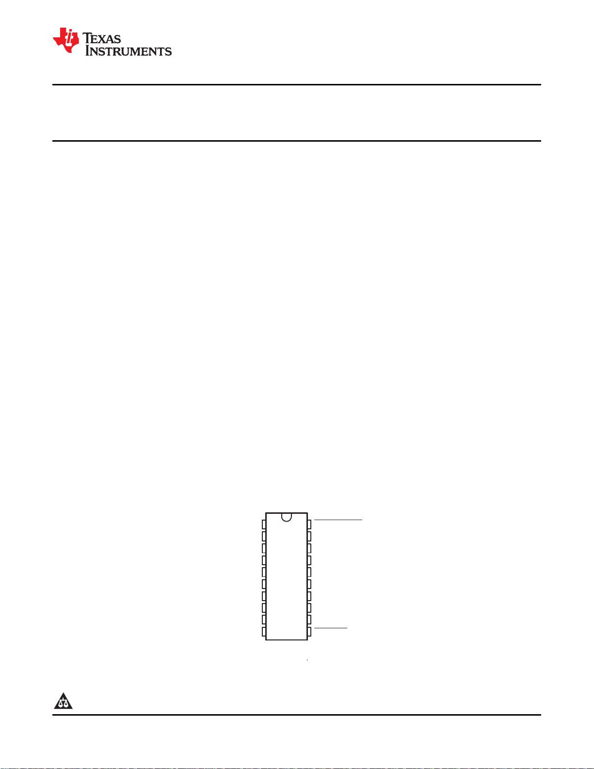
DB OR PW PACKAGE
(TOP VIEW)
TRS3318E
www.ti.com
2.5-V 460-kbps RS-232 TRANSCEIVER
WITH ±15-kV ESD PROTECTION
Check for Samples: TRS3318E
1
FEATURES
• ESD Protection for RS-232 I/O Pins
– ±15 kV (Human-Body Model)
– ±8 kV (IEC 61000-4-2, Contact Discharge)
– ±15 kV (IEC 61000-4-2, Air-Gap Discharge)
• 300-µA Operating Supply Current
• 1-µA Low-Power Standby Mode (With
Receivers Active)
• Designed to Transmit at a Data Rate of
460 kbps
• Auto-Powerdown Plus Option Features
Flexible Power-Saving Mode
• Operates From a Single 2.25-V to 3-V V
Supply
• Designed to be Interchangeable With Industry
Standard '3318 Devices
APPLICATIONS
• Battery-Powered Systems
• PDAs
• Cellular Phones
• Notebooks
• Hand-Held Equipment
• Pagers
CC
SLLS805B –APRIL 2007–REVISED OCTOBER 2013
DESCRIPTION
The TRS3318E is a dual-driver, dual-receiver, RS232-compatible transceiver. The device features
auto-powerdown plus and enhanced electrostatic
discharge (ESD) protection integrated into the chip.
Driver output and receiver input are protected to ±15
kV using the IEC 61000-4-2 Air-Gap Discharge
method, ±8 kV using the IEC 61000-4-2 Contact
Discharge method, and ±15 kV using the HumanBody Model (HBM).
The device operates at a data rate of 460 kbps. The
transceiver has a proprietary low-dropout driver
output stage, enabling RS-232-compatible operation
from a 2.25-V to 3-V supply with a dual charge pump.
The charge pump requires only four 0.1-µF
capacitors and features a logic-level output (READY)
that asserts when the charge pump is regulating and
the device is ready to begin transmitting.
The TRS3318E achieves a 1-µA supply current using
the auto-powerdown feature. This device
automatically enters a low-power power-down mode
when the RS-232 cable is disconnected or the drivers
of the connected peripherals are inactive for more
than 30 s. The device turns on again when it senses
a valid transition at any driver or receiver input. Autopowerdown saves power without changes to the
existing BIOS or operating system.
This device is available in two space-saving
packages: 20-pin SSOP and 20-pin TSSOP.
1
PRODUCTION DATA information is current as of publication date.
Products conform to specifications per the terms of the Texas
Instruments standard warranty. Production processing does not
necessarily include testing of all parameters.
Please be aware that an important notice concerning availability, standard warranty, and use in critical applications of
Texas Instruments semiconductor products and disclaimers thereto appears at the end of this data sheet.
Copyright © 2007–2013, Texas Instruments Incorporated
TRS3318E
SLLS805B –APRIL 2007–REVISED OCTOBER 2013
This integrated circuit can be damaged by ESD. Texas Instruments recommends that all integrated circuits be handled with
appropriate precautions. Failure to observe proper handling and installation procedures can cause damage.
ESD damage can range from subtle performance degradation to complete device failure. Precision integrated circuits may be more
susceptible to damage because very small parametric changes could cause the device not to meet its published specifications.
www.ti.com
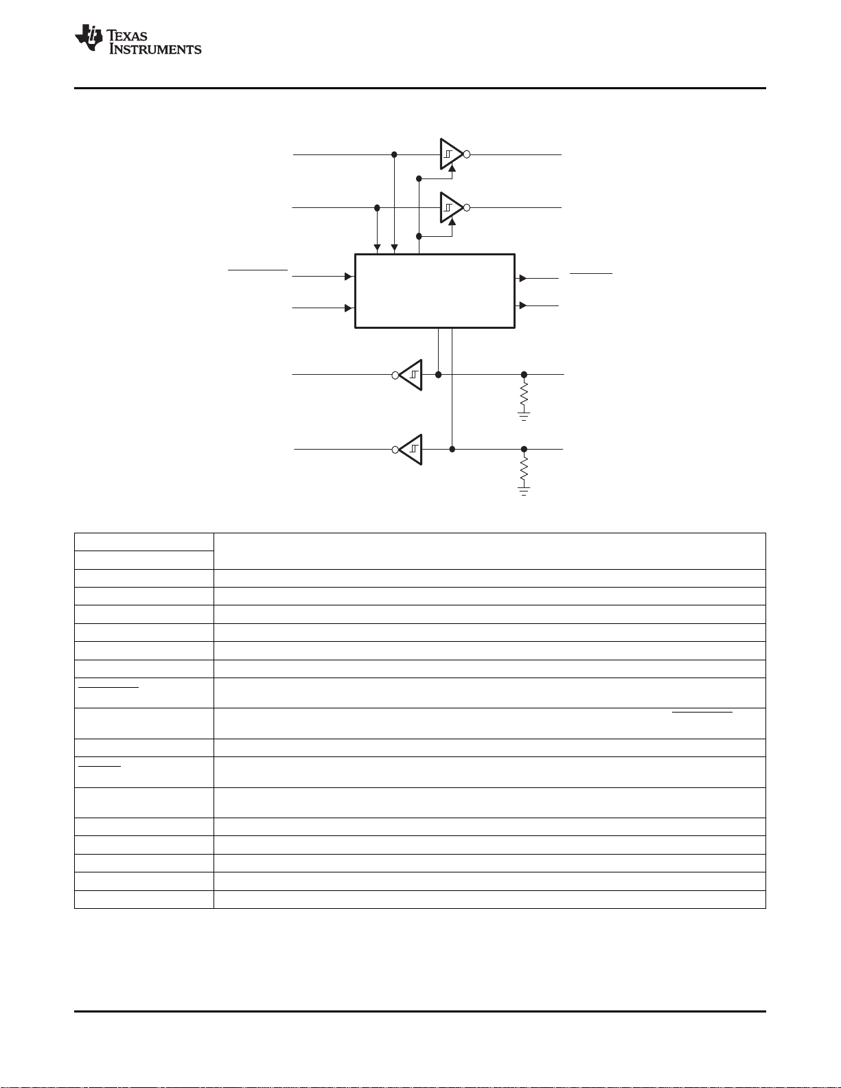
DETAILED DESCRIPTION
Flexible control options for power management are featured when the serial port and driver inputs are inactive.
The auto-powerdown plus feature functions when FORCEON is low and FORCEOFF is high. During this mode of
operation, if the device does not sense valid signal transitions on all receiver and driver inputs for approximately
30 s, the built-in charge pump and drivers are powered down, reducing the supply current to 1 µA. By
disconnecting the serial port or placing the peripheral drivers off, auto-powerdown plus can be disabled when
FORCEON and FORCEOFF are high. With auto-powerdown plus enabled, the device activates automatically
when a valid signal is applied to any receiver or driver input. INVALID is high (valid data) if any receiver input
voltage is greater than 2.7 V or less than –2.7 V, or has been between –0.3 V and 0.3 V for less than 30 µs
(typical number). INVALID is low (invalid data) if all receiver input voltage are between –0.3 V and 0.3 V for more
than 30 µs (typical number).
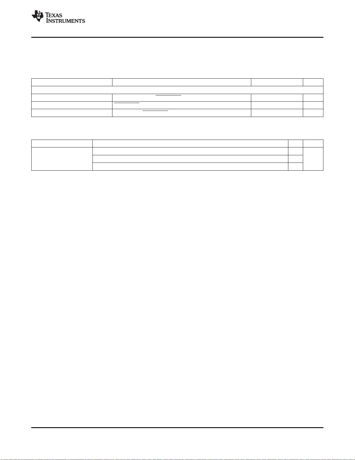
FUNCTION TABLE
INPUT CONDITIONS OUTPUT STATES
RECEIVER
FORCEON FORCEOFF LEVEL DRIVER RECEIVER INVALID READY
H H No No Active Active L H auto-powerdown
H H No Yes Active Active H H auto-powerdown
L H Yes No Active Active L H auto-powerdown
L H Yes Yes Active Active H H auto-powerdown
L H No No Z Active L L auto-powerdown
L H No Yes Z Active H L auto-powerdown
X L X No Z Active L L
X L X Yes Z Active H L
INVALID INVALID X No Z Active L L auto-powerdown
INVALID INVALID X Yes Active Active H H auto-powerdown
(1) H = high level, L = low level, X = irrelevant, Z = high impedance
OR DRIVER
EDGE
WITHIN 30 s
VALID
RS-232
PRESENT AT
RECEIVER
Auto-Powerdown Plus Conditions
Auto-Powerdown Conditions
(1)
OPERATING
MODE
Normal operation,
plus disabled
Normal operation,
plus disabled
Normal operation,
plus enabled
Normal operation,
plus enabled
Power down,
plus enabled
Power down,
plus enabled
Manual power
down
Manual power
down
Power down,
enabled
Normal operation,
enabled
2 Submit Documentation Feedback Copyright © 2007–2013, Texas Instruments Incorporated
Product Folder Links: TRS3318E
DIN2
DIN1
DOUT2
DOUT1
Auto-powerdown Plus
INVALID
RIN1
RIN2
FORCEOFF
FORCEON
ROUT1
ROUT2
13
12
20
14
15
10
17
8
11
16
9
5 k
5 k
Ω
Ω
READY
1
TRS3318E
www.ti.com
SLLS805B –APRIL 2007–REVISED OCTOBER 2013
LOGIC DIAGRAM (POSITIVE LOGIC)
TERMINAL FUNCTIONS
TERMINAL
NAME NO.
C1+ 2 Positive voltage-doubler charge-pump capacitor
C1– 4 Negative voltage-doubler charge-pump capacitor
C2+ 5 Positive inverting charge-pump capacitor
C2– 6 Negative inverting charge-pump capacitor
DIN 12, 13 CMOS driver inputs
DOUT 8, 17 RS-232 driver outputs
FORCEOFF 20
FORCEON 14
GND 18 Ground
INVALID 11
READY 1
RIN 9, 16 RS-232 receiver inputs
ROUT 10, 15 CMOS receiver outputs
V+ 3 2 × VCCgenerated by the charge pump
V– 7 –2 × VCCgenerated by the charge pump
V
CC
Force-off input, active low. Drive low to power down transmitters and charge pump. This overrides autopowerdown and FORCEON (see Function Table).
Force-on input, active high. Drive high to override auto-powerdown, keeping transmitters on (FORCEOFF must
be high) (see Function Table).
Valid signal detector output, active low. A logic high indicates that a valid RS-232 level is present on a receiver
input.
Ready to transmit output, active high. READY is enabled high when V– goes below –3.5 V and the device is
ready to transmit.
19 2.25-V to 3-V single-supply voltage
DESCRIPTION
Copyright © 2007–2013, Texas Instruments Incorporated Submit Documentation Feedback 3
Product Folder Links: TRS3318E
TRS3318E
SLLS805B –APRIL 2007–REVISED OCTOBER 2013
Absolute Maximum Ratings
(1)
www.ti.com
over operating free-air temperature range (unless otherwise noted)
MIN MAX UNIT
VCCto GND –0.3 6 V
V+ to GND
V– to GND
V+ + IV–I
Input voltage V
Output voltage V
Short-circuit duration DOUT to GND Continuous
Continuous power dissipation (TA= 70°C) mW
Storage temperature range –65 150 °C
Lead temperature (soldering, 10 s) 300 °C
(1) Stresses beyond those listed under "absolute maximum ratings" may cause permanent damage to the device. These are stress ratings
(2) V+ and V– can have maximum magnitudes of 7 V, but their absolute difference cannot exceed 13 V.
(2)
(2)
(2)
DIN, FORCEON, FORCEOFF to GND –0.3 6
RIN to GND ±25
DOUT to GND ±13.2
ROUT, INVALID, READY to GND –0.3 VCC+ 0.3
20-pin SSOP (derate 8 mW/°C above 70°C) 640
20-pin TSSOP (derate 7 mW/°C above 70°C) 559
only, and functional operation of the device at these or any other conditions beyond those indicated under "recommended operating
conditions" is not implied. Exposure to absolute-maximum-rated conditions for extended periods may affect device reliability.
–0.3 7 V
–7 0.3 V
13 V
Recommended Operating Conditions
See Figure 4
MIN NOM MAX UNIT
Supply voltage 2.25 2.5 3 V
VIHDriver and control high-level input voltage VCC= 2.5 V to 3 V 0.7 × V
VILDriver and control low-level input voltage VCC= 2.5 V to 3 V 0 0.3 × V
VIReceiver input voltage –25 25 V
TAOperating free-air temperature °C
DIN, FORCEOFF,
FORCEON
DIN, FORCEOFF,
FORCEON
TRS3318EC 0 70
TRS3318EI –40 85
CC
5.5 V
CC
V
4 Submit Documentation Feedback Copyright © 2007–2013, Texas Instruments Incorporated
Product Folder Links: TRS3318E
TRS3318E
www.ti.com
SLLS805B –APRIL 2007–REVISED OCTOBER 2013
Supply Current Section
Electrical Characteristics
over recommended ranges of supply voltage and operating free-air temperature,
VCC= 2.25 V to 3 V, C1–C4 = 0.1 µF, TA= T
PARAMETER TEST CONDITIONS MIN TYP
DC Characteristics (VCC= 2.5 V, TA= 25°C)
Auto-powerdown plus supply current FORCEON = GND, FORCEOFF = VCC, All RIN and DIN idle 1 10 µA
Auto-powerdown supply current FORCEOFF = GND 1 10 µA
Supply current FORCEON = FORCEOFF = VCC, No load 0.3 2 mA
(1) Typical values are at VCC= 2.5 V, TA= 25°C.
MIN
to T
(unless otherwise noted)
MAX
(1)
MAX UNIT
ESD Protection
PARAMETER TEST CONDITIONS TYP UNIT
HBM ±15
RIN, DOUT IEC 61000-4-2 Air-Gap Discharge method ±15 kV
IEC 61000-4-2 Contact Discharge method ±8
Copyright © 2007–2013, Texas Instruments Incorporated Submit Documentation Feedback 5
Product Folder Links: TRS3318E
TRS3318E
SLLS805B –APRIL 2007–REVISED OCTOBER 2013
www.ti.com
Driver Section
Electrical Characteristics
over recommended ranges of supply voltage and operating free-air temperature,
VCC= 2.25 V to 3 V, C1–C4 = 0.1 µF, TA= T
PARAMETER TEST CONDITIONS MIN TYP
Driver input hysteresis 0.3 V
Input leakage current FORCEON, DIN, FORCEOFF ±0.01 ±1 µA
Output voltage swing All driver outputs loaded with 3 kΩ to ground ±3.7 ±4 V
Output resistance VCC= 0, Driver output = ±2 V 300 10M Ω
Output short-circuit current
Output leakage current VCC= 0 or 2.25 V to 3 V, V
(1) Typical values are at VCC= 2.5 V, TA= 25°C.
(2) Short-circuit durations should be controlled to prevent exceeding the device absolute power dissipation ratings, and not more than one
output should be shorted at a time.
(2)
MIN
to T
(unless otherwise noted) (see Figure 4)
MAX
= ±12 V, Drivers disabled ±25 µA
OUT
(1)
MAX UNIT
±25 ±60 mA
Switching Characteristics
over recommended ranges of supply voltage and operating free-air temperature,
VCC= 2.25 V to 3 V, C1–C4 = 0.1 µF, TA= T
PARAMETER TEST CONDITIONS MIN TYP
Maximum data rate RL= 3 kΩ, CL= 1000 pF, One transmitter switching 460 kbps
|t
– t
PHL
| Driver skew
PLH
Transition-region slew rate Measured from 3 V to –3 V or –3 V to 3 V, 4 30 V/µs
(2)
MIN
to T
(unless otherwise noted) (see Figure 1)
MAX
VCC= 2.5 V, TA= 25°C, RL= 3 kΩ to 7 kΩ,
CL= 150 pF to 2500 pF
(1)
MAX UNIT
100 ns
(1) Typical values are at VCC= 2.5 V, TA= 25°C.
(2) Pulse skew is defined as |t
PLH
– t
| of each channel of the same device.
PHL
6 Submit Documentation Feedback Copyright © 2007–2013, Texas Instruments Incorporated
Product Folder Links: TRS3318E
TRS3318E
www.ti.com
SLLS805B –APRIL 2007–REVISED OCTOBER 2013
Receiver Section
Electrical Characteristics
over recommended ranges of supply voltage and operating free-air temperature,
VCC= 2.25 V to 3 V, C1–C4 = 0.1 µF, TA= T
PARAMETER TEST CONDITIONS MIN TYP
Input voltage range –25 25 V
Input threshold low TA= 25°C 0.3 × V
Input threshold high TA= 25°C 0.7 × V
Input hysteresis 0.3 V
Input resistance TA= 25°C 3 5 7 kΩ
Output leakage current ±0.05 ±10 µA
Output voltage low I
Output voltage high I
(1) Typical values are at VCC= 2.5 V, TA= 25°C.
= 0.5 mA 0.1 × V
OUT
= –0.5 mA 0.9 × V
OUT
MIN
to T
(unless otherwise noted) (see Figure 4)
MAX
CC
CC
(1)
MAX UNIT
CC
CC
Switching Characteristics
over recommended ranges of supply voltage and operating free-air temperature,
VCC= 2.25 V to 3 V, C1–C4 = 0.1 µF (unless otherwise noted) (see Figure 4)
(1)
0.175
0.175
50 ns
t
t
|t
PHL
PLH
PHL
Receiver propagation delay RIN to ROUT, CL= 150 pF µs
– t
| Receiver skew
PLH
PARAMETER TEST CONDITIONS TYP
(2)
V
V
V
V
UNIT
(1) Typical values are at VCC= 2.5 V, TA= 25°C.
(2) Pulse skew is defined as |t
PLH
– t
| of each channel of the same device.
PHL
Copyright © 2007–2013, Texas Instruments Incorporated Submit Documentation Feedback 7
Product Folder Links: TRS3318E

TRS3318E
SLLS805B –APRIL 2007–REVISED OCTOBER 2013
www.ti.com
Auto-Powerdown Plus Section
Electrical Characteristics
over recommended ranges of supply voltage and operating free-air temperature,
VCC= 2.25 V to 3 V, C1–C4 = 0.1 µF, TA= T
PARAMETER TEST CONDITIONS MIN MAX UNIT
Receiver input threshold to INVALID high V
Receiver input threshold INVALID low –0.3 0.3 V
INVALID, READY voltage low I
INVALID, READY voltage high I
MIN
to T
(unless otherwise noted) (see Figure 4)
MAX
Positive threshold 2.7
Negative threshold –2.7
= 0.5 mA 0.1 × V
OUT
= –0.5 mA 0.8 × V
OUT
CC
CC
Switching Characteristics
over recommended ranges of supply voltage and operating free-air temperature,
VCC= 2.25 V to 3 V, C1–C4 = 0.1 µF, TA= T
PARAMETER TEST CONDITIONS MIN TYP
t
INVH
t
INVL
t
WU
t
AUTOPRDN
Receiver positive or negative threshold to INVALID high VCC= 2.5 V 1 µs
Receiver positive or negative threshold to INVALID low VCC= 2.5 V 30 µs
Receiver or driver edge to driver enabled VCC= 2.5 V 100 µs
Receiver or driver edge to driver shutdown VCC= 2.5 V 15 30 60 s
MIN
to T
(unless otherwise noted) (see Figure 4)
MAX
(1)
MAX UNIT
V
V
(1) Typical values are at VCC= 2.5 V, TA= 25°C.
8 Submit Documentation Feedback Copyright © 2007–2013, Texas Instruments Incorporated
Product Folder Links: TRS3318E

TEST CIRCUIT VOLTAGE WAVEFORMS
50 Ω
−3 V
3 V
Output
Input
V
OL
V
OH
t
PHL
Generator
(see Note B)
t
PLH
Output
C
L
(see Note A)
NOTES: A. CL includes probe and jig capacitance.
B. The pulse generator has the following characteristics: ZO = 50 Ω, 50% duty cycle, tr ≤ 10 ns, tf ≤ 10 ns.
0 V 0 V
50% 50%
50 Ω
TEST CIRCUIT VOLTAGE WAVEFORMS
0 V
2.25 V
Output
Input
V
OL
V
OH
t
PLH
Generator
(see Note B)
R
L
3 V
FORCEOFF
RS-232
Output
t
PHL
C
L
(see Note A)
NOTES: A. CL includes probe and jig capacitance.
B. The pulse generator has the following characteristics: PRR = 250 kbit/s, ZO = 50 Ω, 50% duty cycle, tr ≤ 10 ns, tf ≤ 10 ns.
50%
50%
1.125 V
1.125 V
50 Ω
TEST CIRCUIT VOLTAGE WAVEFORMS
−3 V
−3 V
3 V
3 V
0 V
3 V
Output
Input
V
OL
V
OH
t
TLH
Generator
(see Note B)
R
L
3 V
FORCEOFF
RS-232
Output
t
THL
C
L
(see Note A)
SR(tr) +
6 V
t
THL
or t
TLH
NOTES: A. CL includes probe and jig capacitance.
B. The pulse generator has the following characteristics: PRR = 250 kbit/s, ZO = 50 Ω, 50% duty cycle, tr ≤ 10 ns, tf ≤ 10 ns.
TRS3318E
www.ti.com
SLLS805B –APRIL 2007–REVISED OCTOBER 2013
PARAMETER MEASUREMENT INFORMATION
Figure 1. Driver Slew Rate
Copyright © 2007–2013, Texas Instruments Incorporated Submit Documentation Feedback 9
Figure 2. Driver Pulse Skew
Figure 3. Receiver Propagation Delay Times
Product Folder Links: TRS3318E

t
WU
V
CC
0
0
V+
V−
V
CC
0
Driver
Inputs
Receiver
Inputs
}
INVALID
Output
Driver
Outputs
V
CC
Invalid
Region
Ready
Output
t
INVH
t
WU
t
INVL
VOLTAGE WAVEFORMS
TEST CIRCUIT
50 Ω
Generator
(see Note B)
ROUT
Auto-powerdown
Plus
INVALID
DOUTDIN
C
L
= 30 pF
(see Note A)
2.7 V
−2.7 V
0.3 V
−0.3 V
0 V
Valid RS-232 Level, INVALID
High
Indeterminate
Indeterminate
If Signal Remains Within This Region
For More Than 30 µs, INVALID
Is Low
†
Valid RS-232 Level, INVALID
High
†
Auto-powerdown disables drivers and reduces supply
current to 1 µA.
FORCEON
FORCEOFF
TRS3318E
SLLS805B –APRIL 2007–REVISED OCTOBER 2013
PARAMETER MEASUREMENT INFORMATION (continued)
www.ti.com
10 Submit Documentation Feedback Copyright © 2007–2013, Texas Instruments Incorporated
Figure 4. INVALID Propagation Delay Times and Supply Enabling Time
Product Folder Links: TRS3318E

14
1
10
15
20
9
GND
18
13
6
5
4
2
RIN1
16
DOUT2
8
V−
7
V+
3
19
2.5 V
5k
5k
RS-232-Compatible
Outputs
RS-232-Compatible
Inputs
To Power-Management Unit
Auto-
powerdown
Plus
C1+
C1−
C2+
C2−
DIN1
DIN2
ROUT1
READY
FORCEON
17
RIN2
11
INVALID
FORCEOFF
0.1 mF
+
+
+
+
+
C3
0.1 mF
C4
0.1 mF
C1
0.1 mF
C2
0.1 mF
C
BYPASS
V
CC
12
ROUT2
DOUT1
RIN1
V
CC
TRS3318E
www.ti.com
SLLS805B –APRIL 2007–REVISED OCTOBER 2013
APPLICATION INFORMATION
Figure 5. Typical Application Circuit
Copyright © 2007–2013, Texas Instruments Incorporated Submit Documentation Feedback 11
Product Folder Links: TRS3318E

TRS3318E
SLLS805B –APRIL 2007–REVISED OCTOBER 2013
www.ti.com
REVISION HISTORY
Changes from Revision A (April 2010) to Revision B Page
• Updated document to new TI datasheet format - no specification changes. ....................................................................... 1
• Removed Ordering Information table. ................................................................................................................................... 2
• Updated TERMINAL FUNCTIONS table to fix inconsistency. .............................................................................................. 3
12 Submit Documentation Feedback Copyright © 2007–2013, Texas Instruments Incorporated
Product Folder Links: TRS3318E

PACKAGE OPTION ADDENDUM
www.ti.com
10-Dec-2020
PACKAGING INFORMATION
Orderable Device Status
TRS3318ECDBR ACTIVE SSOP DB 20 2000 RoHS & Green NIPDAU Level-1-260C-UNLIM 0 to 70 RV18EC
TRS3318ECPW ACTIVE TSSOP PW 20 70 RoHS & Green NIPDAU Level-1-260C-UNLIM 0 to 70 RV18EC
TRS3318ECPWR ACTIVE TSSOP PW 20 2000 RoHS & Green NIPDAU Level-1-260C-UNLIM 0 to 70 RV18EC
TRS3318EIDB ACTIVE SSOP DB 20 70 RoHS & Green NIPDAU Level-1-260C-UNLIM 0 to 70 RV18EI
TRS3318EIDBR ACTIVE SSOP DB 20 2000 RoHS & Green NIPDAU Level-1-260C-UNLIM -40 to 85 RV18EI
TRS3318EIPW ACTIVE TSSOP PW 20 70 RoHS & Green NIPDAU Level-1-260C-UNLIM -40 to 85 RV18EI
TRS3318EIPWR ACTIVE TSSOP PW 20 2000 RoHS & Green NIPDAU Level-1-260C-UNLIM -40 to 85 RV18EI
TRS3318EIPWRG4 ACTIVE TSSOP PW 20 2000 RoHS & Green NIPDAU Level-1-260C-UNLIM -40 to 85 RV18EI
(1)
The marketing status values are defined as follows:
ACTIVE: Product device recommended for new designs.
LIFEBUY: TI has announced that the device will be discontinued, and a lifetime-buy period is in effect.
NRND: Not recommended for new designs. Device is in production to support existing customers, but TI does not recommend using this part in a new design.
PREVIEW: Device has been announced but is not in production. Samples may or may not be available.
OBSOLETE: TI has discontinued the production of the device.
Package Type Package
(1)
Drawing
Pins Package
Qty
Eco Plan
(2)
Lead finish/
Ball material
(6)
MSL Peak Temp
(3)
Op Temp (°C) Device Marking
(4/5)
(2)
RoHS: TI defines "RoHS" to mean semiconductor products that are compliant with the current EU RoHS requirements for all 10 RoHS substances, including the requirement that RoHS substance
do not exceed 0.1% by weight in homogeneous materials. Where designed to be soldered at high temperatures, "RoHS" products are suitable for use in specified lead-free processes. TI may
reference these types of products as "Pb-Free".
RoHS Exempt: TI defines "RoHS Exempt" to mean products that contain lead but are compliant with EU RoHS pursuant to a specific EU RoHS exemption.
Green: TI defines "Green" to mean the content of Chlorine (Cl) and Bromine (Br) based flame retardants meet JS709B low halogen requirements of <=1000ppm threshold. Antimony trioxide based
flame retardants must also meet the <=1000ppm threshold requirement.
(3)
MSL, Peak Temp. - The Moisture Sensitivity Level rating according to the JEDEC industry standard classifications, and peak solder temperature.
(4)
There may be additional marking, which relates to the logo, the lot trace code information, or the environmental category on the device.
(5)
Multiple Device Markings will be inside parentheses. Only one Device Marking contained in parentheses and separated by a "~" will appear on a device. If a line is indented then it is a continuation
of the previous line and the two combined represent the entire Device Marking for that device.
Samples
Addendum-Page 1

PACKAGE OPTION ADDENDUM
www.ti.com
10-Dec-2020
(6)
Lead finish/Ball material - Orderable Devices may have multiple material finish options. Finish options are separated by a vertical ruled line. Lead finish/Ball material values may wrap to two
lines if the finish value exceeds the maximum column width.
Important Information and Disclaimer:The information provided on this page represents TI's knowledge and belief as of the date that it is provided. TI bases its knowledge and belief on information
provided by third parties, and makes no representation or warranty as to the accuracy of such information. Efforts are underway to better integrate information from third parties. TI has taken and
continues to take reasonable steps to provide representative and accurate information but may not have conducted destructive testing or chemical analysis on incoming materials and chemicals.
TI and TI suppliers consider certain information to be proprietary, and thus CAS numbers and other limited information may not be available for release.
In no event shall TI's liability arising out of such information exceed the total purchase price of the TI part(s) at issue in this document sold by TI to Customer on an annual basis.
Addendum-Page 2

PACKAGE MATERIALS INFORMATION
www.ti.com 30-Dec-2020
TAPE AND REEL INFORMATION
*All dimensions are nominal
Device Package
TRS3318ECDBR SSOP DB 20 2000 330.0 16.4 8.2 7.5 2.5 12.0 16.0 Q1
TRS3318ECPWR TSSOP PW 20 2000 330.0 16.4 6.95 7.1 1.6 8.0 16.0 Q1
TRS3318EIDBR SSOP DB 20 2000 330.0 16.4 8.2 7.5 2.5 12.0 16.0 Q1
TRS3318EIPWR TSSOP PW 20 2000 330.0 16.4 6.95 7.0 1.4 8.0 16.0 Q1
Type
Package
Drawing
Pins SPQ Reel
Diameter
(mm)
Reel
Width
W1 (mm)
A0
(mm)B0(mm)K0(mm)P1(mm)W(mm)
Pin1
Quadrant
Pack Materials-Page 1

PACKAGE MATERIALS INFORMATION
www.ti.com 30-Dec-2020
*All dimensions are nominal
Device Package Type Package Drawing Pins SPQ Length (mm) Width (mm) Height (mm)
TRS3318ECDBR SSOP DB 20 2000 853.0 449.0 35.0
TRS3318ECPWR TSSOP PW 20 2000 853.0 449.0 35.0
TRS3318EIDBR SSOP DB 20 2000 853.0 449.0 35.0
TRS3318EIPWR TSSOP PW 20 2000 853.0 449.0 35.0
Pack Materials-Page 2

PACKAGE OUTLINE
A
7.5
6.9
NOTE 3
10
SCALE 2.000
SSOP - 2 mm max heightDB0020A
SMALL OUTLINE PACKAGE
0.1 C
C
SEATING
PLANE
8.2
TYP
7.4
PIN 1 INDEX AREA
18X 0.65
11
20
2X
5.85
0.38
20X
0.22
0.1 C A B
1
B
5.6
5.0
NOTE 4
0 -8
0.25
0.95
0.55
A 15
DETAIL A
TYPICAL
4214851/B 08/2019
SEE DETAIL A
(0.15) TYP
GAGE PLANE
NOTES:
1. All linear dimensions are in millimeters. Any dimensions in parenthesis are for reference only. Dimensioning and tolerancing
per ASME Y14.5M.
2. This drawing is subject to change without notice.
3. This dimension does not include mold flash, protrusions, or gate burrs. Mold flash, protrusions, or gate burrs shall not
exceed 0.15 mm per side.
4. This dimension does not include interlead flash. Interlead flash shall not exceed 0.25 mm per side.
5. Reference JEDEC registration MO-150.
www.ti.com
2 MAX
0.05 MIN

EXAMPLE BOARD LAYOUT
SSOP - 2 mm max heightDB0020A
SMALL OUTLINE PACKAGE
20X (0.45)
18X (0.65)
1
10
20X (1.85)
SYMM
(R0.05) TYP
20
SYMM
11
(7)
LAND PATTERN EXAMPLE
EXPOSED METAL SHOWN
SCALE: 10X
SOLDER MASK
OPENING
EXPOSED METAL
0.07 MAX
ALL AROUND
NON-SOLDER MASK
DEFINED
(PREFERRED)
METAL
15.000
SOLDER MASK DETAILS
METAL UNDER
SOLDER MASK
0.07 MIN
ALL AROUND
SOLDER MASK
DEFINED
NOTES: (continued)
6. Publication IPC-7351 may have alternate designs.
7. Solder mask tolerances between and around signal pads can vary based on board fabrication site.
www.ti.com
SOLDER MASK
OPENING
EXPOSED METAL
4214851/B 08/2019

EXAMPLE STENCIL DESIGN
SSOP - 2 mm max heightDB0020A
SMALL OUTLINE PACKAGE
20X (0.45)
18X (0.65)
1
10
20X (1.85)
SYMM
(R0.05) TYP
20
SYMM
11
(7)
SOLDER PASTE EXAMPLE
BASED ON 0.125 mm THICK STENCIL
SCALE: 10X
4214851/B 08/2019
NOTES: (continued)
8. Laser cutting apertures with trapezoidal walls and rounded corners may offer better paste release. IPC-7525 may have alternate
design recommendations.
9. Board assembly site may have different recommendations for stencil design.
www.ti.com


IMPORTANT NOTICE AND DISCLAIMER
TI PROVIDES TECHNICAL AND RELIABILITY DATA (INCLUDING DATASHEETS), DESIGN RESOURCES (INCLUDING REFERENCE
DESIGNS), APPLICATION OR OTHER DESIGN ADVICE, WEB TOOLS, SAFETY INFORMATION, AND OTHER RESOURCES “AS IS”
AND WITH ALL FAULTS, AND DISCLAIMS ALL WARRANTIES, EXPRESS AND IMPLIED, INCLUDING WITHOUT LIMITATION ANY
IMPLIED WARRANTIES OF MERCHANTABILITY, FITNESS FOR A PARTICULAR PURPOSE OR NON-INFRINGEMENT OF THIRD
PARTY INTELLECTUAL PROPERTY RIGHTS.
These resources are intended for skilled developers designing with TI products. You are solely responsible for (1) selecting the appropriate
TI products for your application, (2) designing, validating and testing your application, and (3) ensuring your application meets applicable
standards, and any other safety, security, or other requirements. These resources are subject to change without notice. TI grants you
permission to use these resources only for development of an application that uses the TI products described in the resource. Other
reproduction and display of these resources is prohibited. No license is granted to any other TI intellectual property right or to any third
party intellectual property right. TI disclaims responsibility for, and you will fully indemnify TI and its representatives against, any claims,
damages, costs, losses, and liabilities arising out of your use of these resources.
TI’s products are provided subject to TI’s Terms of Sale (www.ti.com/legal/termsofsale.html) or other applicable terms available either on
ti.com or provided in conjunction with such TI products. TI’s provision of these resources does not expand or otherwise alter TI’s applicable
warranties or warranty disclaimers for TI products.
Mailing Address: Texas Instruments, Post Office Box 655303, Dallas, Texas 75265
Copyright © 2020, Texas Instruments Incorporated
 Loading...