

Page 1
1
2
3
4
5
6
7
8
9
10
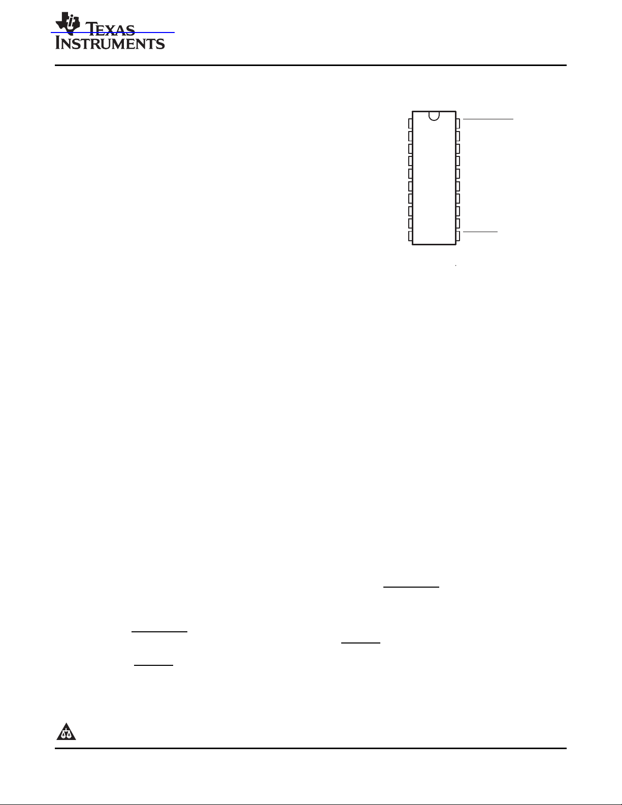
20
19
18
17
16
15
14
13
12
11
READY
C1+
V+
C1−
C2+
C2−
V−
DOUT2
RIN2
ROUT2
FORCEOFF
V
CC
GND
DOUT1
RIN1
ROUT1
FORCEON
DIN1
DIN2
INVALID
DB OR PW PACKAGE
(TOP VIEW)
查询TRS3318IDB供应商
www.ti.com
1
FEATURES
• ESD Protection for RS-232 I/O Pins
– ± 15 kV Human-Body Model (HBM)
– ± 8 kV IEC 61000-4-2, Contact Discharge
– ± 8 kV IEC 61000-4-2, Air-Gap Discharge
• 300- μ A Operating Supply Current
• 1- μ A Low-Power Standby (With Receivers
Active) Mode
• Designed to Transmit at a Data Rate of
460 kbps
• Auto-Powerdown Plus Option Features
Flexible Power-Saving Mode
• Operates From a Single 2.25-V to 3-V V
Supply
APPLICATIONS
• Battery-Powered Systems
• PDAs
• Cellular Phones
• Notebooks
• Hand-Held Equipment
• Pagers
TRS3318
2.5-V 460-kbps RS-232 TRANSCEIVER
WITH ± 15-kV ESD PROTECTION
SLLS820 – AUGUST 2007
CC
DESCRIPTION/ORDERING INFORMATION
The TRS3318 is a dual-driver, dual-receiver, RS-232 compatible transceiver. The device features
auto-powerdown plus and enhanced electrostatic discharge (ESD) protection integrated into the chip. Driver
output and receiver input are protected to ± 8 kV using the IEC 61000-4-2 Air-Gap Discharge method, ± 8 kV
using the IEC 61000-4-2 Contact Discharge method, and ± 15 kV using the Human-Body Model (HBM).
The device operates at a data rate of 460 kbps. The transceiver has a proprietary low-dropout driver output stage
enabling RS-232-compatible operation from a 2.25-V to 3-V supply with a dual charge pump. The charge pump
requires only four 0.1- μ F capacitors and features a logic-level output (READY) that asserts when the charge
pump is regulating and the device is ready to begin transmitting.
The TRS3318 achieves a 1- μ A supply current using the auto-powerdown feature. This device automatically
enters a low-power power-down mode when the RS-232 cable is disconnected or the drivers of the connected
peripherals are inactive for more than 30 s. The device turns on again when it senses a valid transition at any
driver or receiver input. Auto-powerdown saves power without changes to the existing BIOS or operating system.
This device is available in two space-saving packages: 20-pin SSOP and 20-pin TSSOP.
Flexible control options for power management are featured when the serial port and driver inputs are inactive.
The auto-powerdown plus feature functions when FORCEON is low and FORCEOFF is high. During this mode of
operation, if the device does not sense valid signal transitions on all receiver and driver inputs for approximately
30 s, the built-in charge pump and drivers are powered down, reducing the supply current to 1 μ A. By
disconnecting the serial port or placing the peripheral drivers off, auto-powerdown plus can be disabled when
FORCEON and FORCEOFF are high. With auto-powerdown plus enabled, the device activates automatically
when a valid signal is applied to any receiver or driver input. INVALID is high (valid data) if any receiver input
voltage is greater than 2.7 V or less than – 2.7 V, or has been between – 0.3 V and 0.3 V for less than 30 μ s
(typical number). INVALID is low (invalid data) if all receiver input voltage are between – 0.3 V and 0.3 V for more
than 30 μ s (typical number).
1
PRODUCTION DATA information is current as of publication date.
Products conform to specifications per the terms of the Texas
Instruments standard warranty. Production processing does not
necessarily include testing of all parameters.
Please be aware that an important notice concerning availability, standard warranty, and use in critical applications of
Texas Instruments semiconductor products and disclaimers thereto appears at the end of this data sheet.
Copyright © 2007, Texas Instruments Incorporated
Page 2
www.ti.com
TRS3318
2.5-V 460-kbps RS-232 TRANSCEIVER
WITH ± 15-kV ESD PROTECTION
SLLS820 – AUGUST 2007
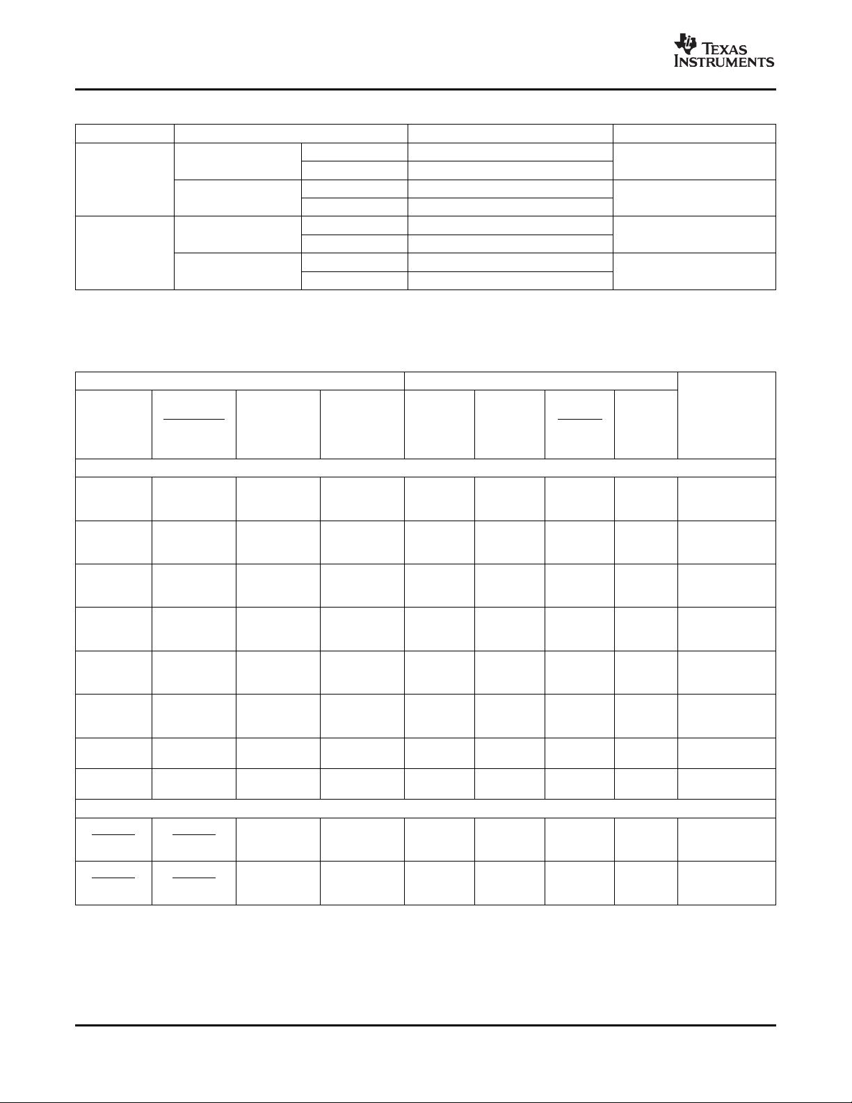
ORDERING INFORMATION
T
A
SSOP – DB RV18C
0 ° C to 70 ° C
TSSOP – PW RV18C
SSOP – DB RV18I
– 40 ° C to 85 ° C
TSSOP – PW RV18I
(1) Package drawings,thermal data, and symbolization are available at www.ti.com/packaging .
(2) For the most current package and ordering information, see the Package Option Addendum at the end of this document, or see the TI
website at www.ti.com .
PACKAGE
(1) (2)
Tube of 70 TRS3318CDB
Reel of 2000 TRS3318CDBR
Tube of 70 TRS3318CPW
Reel of 2000 TRS3318CPWR
Tube of 70 TRS3318IDB
Reel of 2000 TRS3318IDBR
Tube of 70 TRS3318IPW
Reel of 2000 TRS3318IPWR
ORDERABLE PART NUMBER TOP-SIDE MARKING
FUNCTION TABLE
INPUT CONDITIONS OUTPUT STATES
RECEIVER
FORCEON FORCEOFF LEVEL DRIVER RECEIVER INVALID READY
H H No No Active Active L H auto-powerdown
H H No Yes Active Active H H auto-powerdown
L H Yes No Active Active L H auto-powerdown
L H Yes Yes Active Active H H auto-powerdown
L H No No Z Active L L auto-powerdown
L H No Yes Z Active H L auto-powerdown
X L X No Z Active L L
X L X Yes Z Active H L
INVALID INVALID X No Z Active L L auto-powerdown
INVALID INVALID X Yes Active Active H H auto-powerdown
(1) H = high level, L = low level, X = irrelevant, Z = high impedance
OR DRIVER
EDGE
WITHIN 30 s
VALID
RS-232
PRESENT AT
RECEIVER
Auto-Powerdown Plus Conditions
Auto-Powerdown Conditions
(1)
OPERATING
MODE
Normal operation,
plus disabled
Normal operation,
plus disabled
Normal operation,
plus enabled
Normal operation,
plus enabled
Power down,
plus enabled
Power down,
plus enabled
Manual power
down
Manual power
down
Power down,
enabled
Normal operation,
enabled
2 Submit Documentation Feedback Copyright © 2007, Texas Instruments Incorporated
Product Folder Link(s): TRS3318
Page 3
www.ti.com
DIN2
DIN1
DOUT2
DOUT1
Auto-Powerdown Plus
INVALID
RIN1
RIN2
FORCEOFF
FORCEON
ROUT1
ROUT2
13
12
20
14
15
10
17
8
11
16
9
5 k
5 k
Ω
Ω
READY
1
LOGIC DIAGRAM (POSITIVE LOGIC)
TRS3318
2.5-V 460-kbps RS-232 TRANSCEIVER
WITH ± 15-kV ESD PROTECTION
SLLS820 – AUGUST 2007
TERMINAL FUNCTIONS
TERMINAL
NAME NO.
C1+ 2 Positive voltage-doubler charge-pump capacitor
C1 – 4 Negative voltage-doubler charge-pump capacitor
C2+ 5 Positive inverting charge-pump capacitor
C2 – 6 Negative inverting charge-pump capacitor
DIN 12, 13 CMOS driver inputs
DOUT 8, 17 RS-232 driver outputs
FORCEOFF 20
FORCEON 14
GND 18 Ground
INVALID 11
READY 1
RIN 9, 16 RS-232 receiver inputs
ROUT 10, 15 CMOS receiver outputs
V+ 3 2 × V
V – 7 – 2 × V
V
CC
Force-off input, active low. Drive low to power down transmitters, receivers, and charge pump. This overrides
auto-powerdown and FORCEON (see Function Table).
Force-on input, active high. Drive high to override auto-powerdown, keeping transmitters and receivers on
( FORCEOFF must be high) (see Function Table).
Valid signal detector output, active low. A logic high indicates that a valid RS-232 level is present on a receiver
input.
Ready to transmit output, active high. READY is enabled high when V – goes below – 3.5 V and the device is
ready to transmit.
generated by the charge pump
CC
generated by the charge pump
CC
19 2.25-V to 3-V single-supply voltage
DESCRIPTION
Copyright © 2007, Texas Instruments Incorporated Submit Documentation Feedback 3
Product Folder Link(s): TRS3318
Page 4
www.ti.com
TRS3318
2.5-V 460-kbps RS-232 TRANSCEIVER
WITH ± 15-kV ESD PROTECTION
SLLS820 – AUGUST 2007
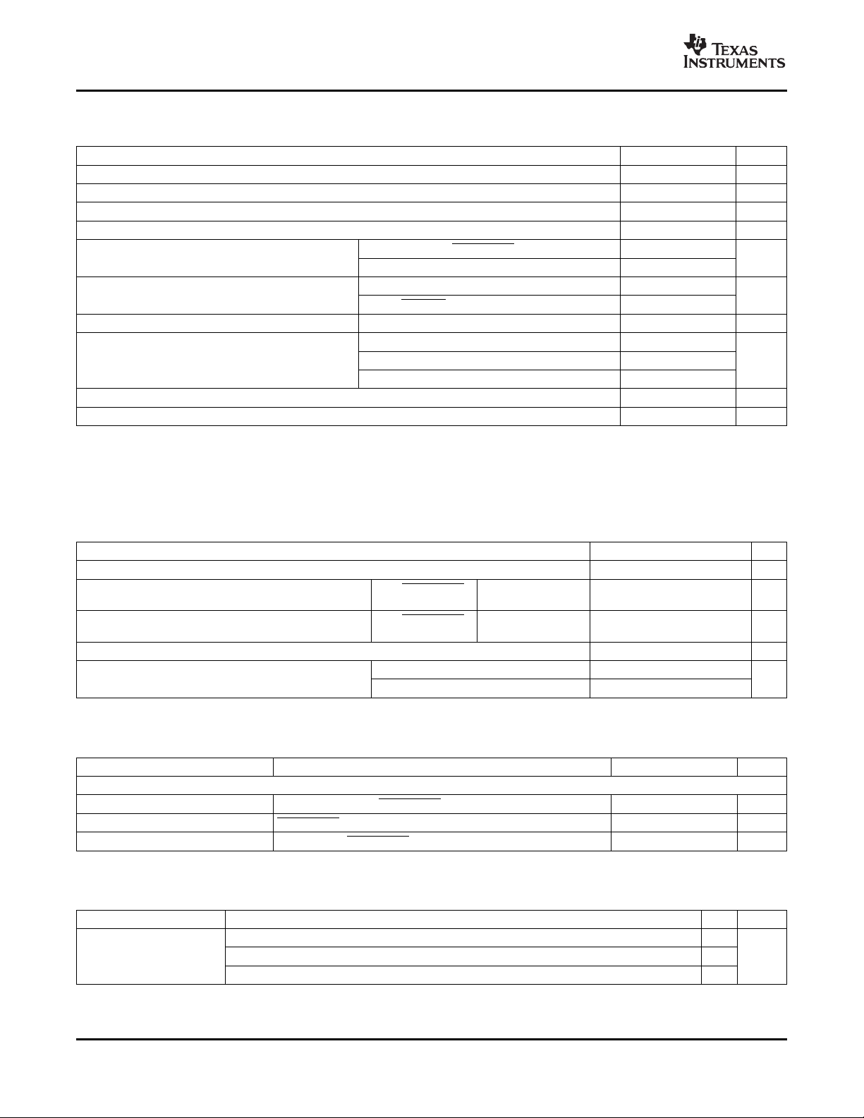
Absolute Maximum Ratings
(1)
over operating free-air temperature range (unless otherwise noted)
MIN MAX UNIT
V
CC
V+ Positive supply voltage range
V – Negative supply voltage range
V+ + IV – I Supply voltage differential
V
I
V
O
Supply voltage range – 0.3 6 V
(2)
(2)
(2)
Input voltage V
Output voltage V
DIN, FORCEON, FORCEOFF to GND – 0.3 6
RIN to GND ± 25
DOUT to GND ± 13.2
ROUT, INVALID, READY to GND – 0.3 V
– 0.3 7 V
– 7 0.3 V
CC
Short-circuit duration DOUT to GND Continuous
16-pin SSOP (derate 7.14 mW/ ° C above 70 ° C) 571
Continuous power dissipation
(T
= 70 ° C)
A
T
stg
Storage temperature range – 65 150 ° C
20-pin SSOP (derate 8 mW/ ° C above 70 ° C 640 mW
20-pin TSSOP (derate 7 mW/ ° C above 70 ° C) 559
Lead temperature (soldering, 10 s) 300 ° C
(1) Stresses beyond those listed under "absolute maximum ratings" may cause permanent damage to the device. These are stress ratings
only, and functional operation of the device at these or any other conditions beyond those indicated under "recommended operating
conditions" is not implied. Exposure to absolute-maximum-rated conditions for extended periods may affect device reliability.
(2) V+ and V – can have maximum magnitudes of 7 V, but their absolute difference cannot exceed 13 V.
Recommended Operating Conditions
See Figure 4
MIN NOM MAX UNIT
Supply voltage 2.25 2.5 3 V
V
Driver and control high-level input voltage V
IH
V
Driver and control low-level input voltage V
IL
V
Receiver input voltage – 25 25 V
I
T
Operating free-air temperature ° C
A
DIN, FORCEOFF,
FORCEON
DIN, FORCEOFF,
FORCEON
= 2.5 V to 3 V 0.7 × V
CC
= 2.5 V to 3 V 0 0.3 × V
CC
CC
TRS3318C 0 70
TRS3318I – 40 85
+ 0.3
13 V
5.5 V
CC
V
Electrical Characteristics
V
= 2.25 V to 3 V, C1 – C4 = 0.1 μ F, TA= T
CC
PARAMETER TEST CONDITIONS MIN TYP
DC Characteristics (V
= 2.5 V, TA= 25 ° C)
CC
to T
MIN
(unless otherwise noted)
MAX
(1)
MAX UNIT
Auto-powerdown plus supply current FORCEON = GND, FORCEOFF = VCC, All RIN and DIN idle 1 10 μ A
Auto-powerdown supply current FORCEOFF = GND 1 10 μ A
Supply current FORCEON = FORCEOFF = VCC, No load 0.3 2 mA
(1) Typical values are at V
= 2.5 V, TA= 25 ° C.
CC
ESD Protection
PARAMETER TEST CONDITIONS TYP UNIT
Human-Body Model (HBM) ± 15
RIN, DOUT IEC 61000-4-2 Air-Gap Discharge method ± 8 kV
IEC 61000-4-2 Contact Discharge method ± 8
4 Submit Documentation Feedback Copyright © 2007, Texas Instruments Incorporated
Product Folder Link(s): TRS3318
Page 5
www.ti.com
TRS3318
2.5-V 460-kbps RS-232 TRANSCEIVER
WITH ± 15-kV ESD PROTECTION
SLLS820 – AUGUST 2007
DRIVER SECTION
Electrical Characteristics
over recommended ranges of supply voltage and operating free-air temperature,
V
= 2.25 V to 3 V, C1 – C4 = 0.1 μ F, TA= T
CC
PARAMETER TEST CONDITIONS MIN TYP
V
hys
I
on
V
om
r
O
I
OS
I
off
(1) Typical values are at V
(2) Short-circuit durations should be controlled to prevent exceeding the device absolute power dissipation ratings, and not more than one
Driver input hysteresis 0.3 V
Input leakage current FORCEON, DIN, FORCEOFF ± 0.01 ± 1 μ A
Output voltage swing All driver outputs loaded with 3 k Ω to ground ± 3.7 ± 4 V
Output resistance V
Output short-circuit current
(2)
Output leakage current ± 25 μ A
= 2.5 V, TA= 25 ° C.
CC
output should be shorted at a time.
Switching Characteristics
over recommended ranges of supply voltage and operating free-air temperature,
V
= 2.25 V to 3 V, C1 – C4 = 0.1 μ F, TA= T
CC
PARAMETER TEST CONDITIONS MIN TYP
Maximum data rate RL= 3 k Ω , CL= 1000 pF, One transmitter switching 460 kbps
|t
– t
PHL
| Driver skew
PLH
SR(tr) Transition-region slew rate Measured from 3 V to – 3 V or – 3 V to 3 V, 4 30 V/ μ s
(1) Typical values are at V
(2) Pulse skew is defined as |t
(2)
= 2.5 V, TA= 25 ° C.
CC
PLH
– t
| of each channel of the same device.
PHL
to T
MIN
V
disabled
to T
MIN
V
CC
(unless otherwise noted) (see Figure 4 )
MAX
= 0, Driver output = ± 2 V 300 10M Ω
CC
= 0 or 2.25 V to 3 V, V
CC
(unless otherwise noted) (see Figure 1 )
MAX
= ± 12 V, Drivers
OUT
= 2.5 V, TA= 25 ° C, RL= 3 k Ω to 7 k Ω ,
CL= 150 pF to 2500 pF
(1)
MAX UNIT
± 25 ± 60 mA
(1)
MAX UNIT
100 ns
Copyright © 2007, Texas Instruments Incorporated Submit Documentation Feedback 5
Product Folder Link(s): TRS3318
Page 6
www.ti.com
TRS3318
2.5-V 460-kbps RS-232 TRANSCEIVER
WITH ± 15-kV ESD PROTECTION
SLLS820 – AUGUST 2007
RECEIVER SECTION
Electrical Characteristics
over recommended ranges of supply voltage and operating free-air temperature,
V
= 2.25 V to 3 V, C1 – C4 = 0.1 μ F, TA= T
CC
PARAMETER TEST CONDITIONS MIN TYP
V
I
V
IT+
V
IT –
V
hys
r
i
I
off
V
OL
V
OH
(1) Typical values are at V
Input voltage range – 25 25 V
Input voltage threshold low TA= 25 ° C 0.3 × V
Input voltage threshold high TA= 25 ° C 0.7 × V
Input hysteresis 0.3 V
Input resistance TA= 25 ° C 3 5 7 k Ω
Output leakage current ± 0.05 ± 10 μ A
Output voltage low I
Output voltage high I
= 2.5 V, TA= 25 ° C.
CC
Switching Characteristics
over recommended ranges of supply voltage and operating free-air temperature,
V
= 2.25 V to 3 V, C1 – C4 = 0.1 μ F, TA= T
CC
PARAMETER TEST CONDITIONS TYP
t
PHL
t
PLH
|t
– t
PHL
PLH
(1) Typical values are at V
(2) Pulse skew is defined as |t
Receiver propagation delay RIN to ROUT, CL= 150 pF μ s
| Receiver skew
(2)
= 2.5 V, TA= 25 ° C.
CC
– t
PLH
| of each channel of the same device.
PHL
to T
MIN
MAX
to T
MIN
MAX
(unless otherwise noted) (see Figure 4 )
CC
= 0.5 mA 0.1 × V
OUT
= – 0.5 mA 0.9 × V
OUT
CC
(unless otherwise noted) (see Figure 4 )
(1)
MAX UNIT
V
CC
V
V
CC
V
(1)
UNIT
0.175
0.175
50 ns
6 Submit Documentation Feedback Copyright © 2007, Texas Instruments Incorporated
Product Folder Link(s): TRS3318
Page 7

www.ti.com
TRS3318
2.5-V 460-kbps RS-232 TRANSCEIVER
WITH ± 15-kV ESD PROTECTION
SLLS820 – AUGUST 2007
AUTO-POWERDOWN PLUS SECTION
Electrical Characteristics
over recommended ranges of supply voltage and operating free-air temperature,
V
= 2.25 V to 3 V, C1 – C4 = 0.1 μ F, TA= T
CC
PARAMETER TEST CONDITIONS MIN MAX UNIT
Receiver input threshold to INVALID high V
Receiver input threshold INVALID low – 0.3 0.3 V
INVALID, READY voltage low I
INVALID, READY voltage high I
Switching Characteristics
over recommended ranges of supply voltage and operating free-air temperature,
V
= 2.25 V to 3 V, C1 – C4 = 0.1 μ F, TA= T
CC
PARAMETER TEST CONDITIONS MIN TYP
t
INVH
t
INVL
t
WU
t
AUTOPRDN
(1) Typical values are at V
Receiver positive or negative threshold to INVALID high V
Receiver positive or negative threshold to INVALID low V
Receiver or driver edge to driver enabled V
Receiver or driver edge to driver shutdown V
= 2.5 V,T
CC
= 25 ° C.
A
to T
MIN
(unless otherwise noted) (see Figure 4 )
MAX
Positive threshold 2.7
Negative threshold – 2.7
= 0.5 mA 0.1 × V
OUT
= – 0.5 mA 0.8 × V
OUT
to T
MIN
(unless otherwise noted) (see Figure 4 )
MAX
= 2.5 V 1 μ s
CC
= 2.5 V 30 μ s
CC
= 2.5 V 100 μ s
CC
= 2.5 V 15 30 60 s
CC
CC
CC
(1)
MAX UNIT
V
V
Copyright © 2007, Texas Instruments Incorporated Submit Documentation Feedback 7
Product Folder Link(s): TRS3318
Page 8

www.ti.com
50 Ω
TEST CIRCUIT VOLTAGE WAVEFORMS
−3 V
−3 V
3 V
3 V
0 V
3 V
Output
Input
V
OL
V
OH
t
TLH
Generator
(see Note B)
R
L
3 V
FORCEOFF
RS-232
Output
t
THL
C
L
(see Note A)
SR(tr) +
6 V
t
THL
or t
TLH
NOTES: A. CL includes probe and jig capacitance.
B. The pulse generator has the following characteristics: PRR = 250 kbit/s, ZO = 50 Ω, 50% duty cycle, tr ≤ 10 ns, tf ≤ 10 ns.
50 Ω
TEST CIRCUIT VOLTAGE WAVEFORMS
0 V
2.25 V
Output
Input
V
OL
V
OH
t
PLH
Generator
(see Note B)
R
L
3 V
FORCEOFF
RS-232
Output
t
PHL
C
L
(see Note A)
NOTES: A. CL includes probe and jig capacitance.
B. The pulse generator has the following characteristics: PRR = 250 kbit/s, ZO = 50 Ω, 50% duty cycle, tr ≤ 10 ns, tf ≤ 10 ns.
50%
50%
1.125 V
1.125 V
TEST CIRCUIT VOLTAGE WAVEFORMS
50 Ω
−3 V
3 V
Output
Input
V
OL
V
OH
t
PHL
Generator
(see Note B)
t
PLH
Output
C
L
(see Note A)
NOTES: A. CL includes probe and jig capacitance.
B. The pulse generator has the following characteristics: ZO = 50 Ω, 50% duty cycle, tr ≤ 10 ns, tf ≤ 10 ns.
0 V 0 V
50% 50%
TRS3318
2.5-V 460-kbps RS-232 TRANSCEIVER
WITH ± 15-kV ESD PROTECTION
SLLS820 – AUGUST 2007
PARAMETER MEASUREMENT INFORMATION
Figure 1. Driver Slew Rate
8 Submit Documentation Feedback Copyright © 2007, Texas Instruments Incorporated
Figure 2. Driver Pulse Skew
Figure 3. Receiver Propagation Delay Times
Product Folder Link(s): TRS3318
Page 9

www.ti.com
PARAMETER MEASUREMENT INFORMATION
t
WU
V
CC
0
0
V+
V−
V
CC
0
Driver
Inputs
Receiver
Inputs
}
INVALID
Output
Driver
Outputs
V
CC
Invalid
Region
Ready
Output
t
INVH
t
WU
t
INVL
VOLTAGE WAVEFORMS
TEST CIRCUIT
50 Ω
Generator
(see Note B)
ROUT
Auto-Powerdown
Plus
INVALID
DOUTDIN
C
L
= 30 pF
(see Note A)
2.7 V
−2.7 V
0.3 V
−0.3 V
0 V
Valid RS-232 Level, INVALID High
Indeterminate
Indeterminate
If Signal Remains Within This Region
For More Than 30 µs, INVALID
Is Low
†
Valid RS-232 Level, INVALID
High
†
Auto power down disables drivers and reduces supply
current to 1 µA.
FORCEON
FORCEOFF
TRS3318
2.5-V 460-kbps RS-232 TRANSCEIVER
WITH ± 15-kV ESD PROTECTION
SLLS820 – AUGUST 2007
Figure 4. INVALID Propagation Delay Times and Supply Enabling Time
Copyright © 2007, Texas Instruments Incorporated Submit Documentation Feedback 9
Product Folder Link(s): TRS3318
Page 10

www.ti.com
14
1
10
15
20
9
GND
18
13
6
5
4
2
RIN1
16
DOUT2
8
V−
7
V+
3
19
2.5 V
5k
5k
RS-232-Compatible
Outputs
RS-232-Compatible
Inputs
To Power-Management Unit
Auto-Powerdown
Plus
C1+
C1−
C2+
C2−
DIN1
DIN2
ROUT1
READY
FORCEON
17
RIN2
11
INVALID
FORCEOFF
0.1 mF
+
+
+
+
+
C3
0.1 mF
C4
0.1 mF
C1
0.1 mF
C2
0.1 mF
C
BYPASS
V
CC
12
ROUT2
DOUT1
RIN1
V
CC
TRS3318
2.5-V 460-kbps RS-232 TRANSCEIVER
WITH ± 15-kV ESD PROTECTION
SLLS820 – AUGUST 2007
APPLICATION INFORMATION
Figure 5. Typical Application Circuit
10 Submit Documentation Feedback Copyright © 2007, Texas Instruments Incorporated
Product Folder Link(s): TRS3318
Page 11
PACKAGE OPTION ADDENDUM
www.ti.com
26-Sep-2007
PACKAGING INFORMATION
Orderable Device Status
(1)
Package
Type
Package
Drawing
Pins Package
Qty
Eco Plan
TRS3318CDB ACTIVE SSOP DB 20 70 Green (RoHS &
no Sb/Br)
TRS3318CDBG4 ACTIVE SSOP DB 20 70 Green (RoHS &
no Sb/Br)
TRS3318CDBR ACTIVE SSOP DB 20 2000 Green (RoHS &
no Sb/Br)
TRS3318CDBRG4 ACTIVE SSOP DB 20 2000 Green (RoHS &
no Sb/Br)
TRS3318CPW ACTIVE TSSOP PW 20 70 Green (RoHS &
no Sb/Br)
TRS3318CPWG4 ACTIVE TSSOP PW 20 70 Green (RoHS &
no Sb/Br)
TRS3318CPWR ACTIVE TSSOP PW 20 2000 Green (RoHS &
no Sb/Br)
TRS3318CPWRG4 ACTIVE TSSOP PW 20 2000 Green (RoHS &
no Sb/Br)
TRS3318IDB ACTIVE SSOP DB 20 70 Green (RoHS &
no Sb/Br)
TRS3318IDBG4 ACTIVE SSOP DB 20 70 Green (RoHS &
no Sb/Br)
TRS3318IDBR ACTIVE SSOP DB 20 2000 Green (RoHS &
no Sb/Br)
TRS3318IDBRG4 ACTIVE SSOP DB 20 2000 Green (RoHS &
no Sb/Br)
TRS3318IPW ACTIVE TSSOP PW 20 70 Green (RoHS &
no Sb/Br)
TRS3318IPWG4 ACTIVE TSSOP PW 20 70 Green (RoHS &
no Sb/Br)
TRS3318IPWR ACTIVE TSSOP PW 20 2000 Green (RoHS &
no Sb/Br)
TRS3318IPWRG4 ACTIVE TSSOP PW 20 2000 Green (RoHS &
no Sb/Br)
(1)
The marketing status values are defined as follows:
ACTIVE: Product device recommended for new designs.
LIFEBUY: TI has announced that the device will be discontinued, and a lifetime-buy period is in effect.
NRND: Not recommended for new designs. Device is in production to support existing customers, but TI does not recommend using this part in
a new design.
PREVIEW: Device has been announced but is not in production. Samples may or may not be available.
OBSOLETE: TI has discontinued the production of the device.
(2)
Lead/Ball Finish MSL Peak Temp
CU NIPDAU Level-1-260C-UNLIM
CU NIPDAU Level-1-260C-UNLIM
CU NIPDAU Level-1-260C-UNLIM
CU NIPDAU Level-1-260C-UNLIM
CU NIPDAU Level-1-260C-UNLIM
CU NIPDAU Level-1-260C-UNLIM
CU NIPDAU Level-1-260C-UNLIM
CU NIPDAU Level-1-260C-UNLIM
CU NIPDAU Level-1-260C-UNLIM
CU NIPDAU Level-1-260C-UNLIM
CU NIPDAU Level-1-260C-UNLIM
CU NIPDAU Level-1-260C-UNLIM
CU NIPDAU Level-1-260C-UNLIM
CU NIPDAU Level-1-260C-UNLIM
CU NIPDAU Level-1-260C-UNLIM
CU NIPDAU Level-1-260C-UNLIM
(3)
(2)
Eco Plan - The planned eco-friendly classification: Pb-Free (RoHS), Pb-Free (RoHS Exempt), or Green (RoHS & no Sb/Br) - please check
http://www.ti.com/productcontent for the latest availability information and additional product content details.
TBD: The Pb-Free/Green conversion plan has not been defined.
Pb-Free (RoHS): TI's terms "Lead-Free" or "Pb-Free" mean semiconductor products that are compatible with the current RoHS requirements
for all 6 substances, including the requirement that lead not exceed 0.1% by weight in homogeneous materials. Where designed to be soldered
at high temperatures, TI Pb-Free products are suitable for use in specified lead-free processes.
Pb-Free (RoHS Exempt): This component has a RoHS exemption for either 1) lead-based flip-chip solder bumps used between the die and
package, or 2) lead-based die adhesive used between the die and leadframe. The component is otherwise considered Pb-Free (RoHS
compatible) as defined above.
Green (RoHS & no Sb/Br): TI defines "Green" to mean Pb-Free (RoHS compatible), and free of Bromine (Br) and Antimony (Sb) based flame
retardants (Br or Sb do not exceed 0.1% by weight in homogeneous material)
Addendum-Page 1
Page 12

PACKAGE OPTION ADDENDUM
www.ti.com
(3)
MSL, Peak Temp. -- The Moisture Sensitivity Level rating according to the JEDEC industry standard classifications, and peak solder
temperature.
Important Information and Disclaimer:The information provided on this page represents TI's knowledge and belief as of the date that it is
provided. TI bases its knowledge and belief on information provided by third parties, and makes no representation or warranty as to the
accuracy of such information. Efforts are underway to better integrate information from third parties. TI has taken and continues to take
reasonable steps to provide representative and accurate information but may not have conducted destructive testing or chemical analysis on
incoming materials and chemicals. TI and TI suppliers consider certain information to be proprietary, and thus CAS numbers and other limited
information may not be available for release.
In no event shall TI's liability arising out of such information exceed the total purchase price of the TI part(s) at issue in this document sold by TI
to Customer on an annual basis.
26-Sep-2007
Addendum-Page 2
Page 13

PACKAGE MATERIALS INFORMATION
www.ti.com
TAPE AND REEL BOX INFORMATION
4-Oct-2007
Device Package Pins Site Reel
Diameter
(mm)
TRS3318CDBR DB 20 SITE 41 330 16 8.2 7.5 2.5 12 16 Q1
TRS3318CPWR PW 20 SITE 41 330 16 6.95 7.1 1.6 8 16 Q1
TRS3318IDBR DB 20 SITE 41 330 16 8.2 7.5 2.5 12 16 Q1
TRS3318IPWR PW 20 SITE 41 330 16 6.95 7.1 1.6 8 16 Q1
Reel
Width
(mm)
A0 (mm) B0 (mm) K0 (mm) P1
(mm)W(mm)
Pin1
Quadrant
Pack Materials-Page 1
Page 14
PACKAGE MATERIALS INFORMATION
www.ti.com
4-Oct-2007
Device Package Pins Site Length (mm) Width (mm) Height (mm)
TRS3318CDBR DB 20 SITE 41 346.0 346.0 33.0
TRS3318CPWR PW 20 SITE 41 346.0 346.0 33.0
TRS3318IDBR DB 20 SITE 41 346.0 346.0 33.0
TRS3318IPWR PW 20 SITE 41 346.0 346.0 33.0
Pack Materials-Page 2
Page 15

MECHANICAL DATA
MSSO002E – JANUARY 1995 – REVISED DECEMBER 2001
DB (R-PDSO-G**) PLASTIC SMALL-OUTLINE
28 PINS SHOWN
0,65
28
1
2,00 MAX
0,38
0,22
15
14
A
0,05 MIN
0,15
M
5,60
5,00
Seating Plane
8,20
7,40
0,10
0,25
0,09
0°–ā8°
Gage Plane
0,25
0,95
0,55
PINS **
DIM
A MAX
A MIN
NOTES: A. All linear dimensions are in millimeters.
B. This drawing is subject to change without notice.
C. Body dimensions do not include mold flash or protrusion not to exceed 0,15.
D. Falls within JEDEC MO-150
14
6,50
6,50
5,905,90
2016
7,50
6,90
24
8,50
28
10,50
9,907,90
30
10,50
9,90
38
12,90
12,30
4040065 /E 12/01
POST OFFICE BOX 655303 • DALLAS, TEXAS 75265
Page 16

MECHANICAL DATA
MTSS001C – JANUARY 1995 – REVISED FEBRUARY 1999
PW (R-PDSO-G**) PLASTIC SMALL-OUTLINE PACKAGE
14 PINS SHOWN
0,65
1,20 MAX
14
0,30
0,19
8
4,50
4,30
PINS **
7
Seating Plane
0,15
0,05
8
1
A
DIM
14
0,10
6,60
6,20
0,10
M
0,15 NOM
Gage Plane
0,25
0°–8°
2016
24
28
0,75
0,50
A MAX
A MIN
NOTES: A. All linear dimensions are in millimeters.
B. This drawing is subject to change without notice.
C. Body dimensions do not include mold flash or protrusion not to exceed 0,15.
D. Falls within JEDEC MO-153
3,10
2,90
5,10
4,90
5,10
4,90
6,60
6,40
7,90
7,70
9,80
9,60
4040064/F 01/97
POST OFFICE BOX 655303 • DALLAS, TEXAS 75265
Page 17

IMPORTANT NOTICE
Texas Instruments Incorporated and its subsidiaries (TI) reserve the right to make corrections, modifications, enhancements,
improvements, and other changes to its products and services at any time and to discontinue any product or service without notice.
Customers should obtain the latest relevant information before placing orders and should verify that such information is current and
complete. All products are sold subject to TI’s terms and conditions of sale supplied at the time of order acknowledgment.
TI warrants performance of its hardware products to the specifications applicable at the time of sale in accordance with TI’s
standard warranty. Testing and other quality control techniques are used to the extent TI deems necessary to support this
warranty. Except where mandated by government requirements, testing of all parameters of each product is not necessarily
performed.
TI assumes no liability for applications assistance or customer product design. Customers are responsible for their products and
applications using TI components. To minimize the risks associated with customer products and applications, customers should
provide adequate design and operating safeguards.
TI does not warrant or represent that any license, either express or implied, is granted under any TI patent right, copyright, mask
work right, or other TI intellectual property right relating to any combination, machine, or process in which TI products or services
are used. Information published by TI regarding third-party products or services does not constitute a license from TI to use such
products or services or a warranty or endorsement thereof. Use of such information may require a license from a third party under
the patents or other intellectual property of the third party, or a license from TI under the patents or other intellectual property of TI.
Reproduction of TI information in TI data books or data sheets is permissible only if reproduction is without alteration and is
accompanied by all associated warranties, conditions, limitations, and notices. Reproduction of this information with alteration is an
unfair and deceptive business practice. TI is not responsible or liable for such altered documentation. Information of third parties
may be subject to additional restrictions.
Resale of TI products or services with statements different from or beyond the parameters stated by TI for that product or service
voids all express and any implied warranties for the associated TI product or service and is an unfair and deceptive business
practice. TI is not responsible or liable for any such statements.
TI products are not authorized for use in safety-critical applications (such as life support) where a failure of the TI product would
reasonably be expected to cause severe personal injury or death, unless officers of the parties have executed an agreement
specifically governing such use. Buyers represent that they have all necessary expertise in the safety and regulatory ramifications
of their applications, and acknowledge and agree that they are solely responsible for all legal, regulatory and safety-related
requirements concerning their products and any use of TI products in such safety-critical applications, notwithstanding any
applications-related information or support that may be provided by TI. Further, Buyers must fully indemnify TI and its
representatives against any damages arising out of the use of TI products in such safety-critical applications.
TI products are neither designed nor intended for use in military/aerospace applications or environments unless the TI products are
specifically designated by TI as military-grade or "enhanced plastic." Only products designated by TI as military-grade meet military
specifications. Buyers acknowledge and agree that any such use of TI products which TI has not designated as military-grade is
solely at the Buyer's risk, and that they are solely responsible for compliance with all legal and regulatory requirements in
connection with such use.
TI products are neither designed nor intended for use in automotive applications or environments unless the specific TI products
are designated by TI as compliant with ISO/TS 16949 requirements. Buyers acknowledge and agree that, if they use any
non-designated products in automotive applications, TI will not be responsible for any failure to meet such requirements.
Following are URLs where you can obtain information on other Texas Instruments products and application solutions:
Products Applications
Amplifiers amplifier.ti.com Audio www.ti.com/audio
Data Converters dataconverter.ti.com Automotive www.ti.com/automotive
DSP dsp.ti.com Broadband www.ti.com/broadband
Interface interface.ti.com Digital Control www.ti.com/digitalcontrol
Logic logic.ti.com Military www.ti.com/military
Power Mgmt power.ti.com Optical Networking www.ti.com/opticalnetwork
Microcontrollers microcontroller.ti.com Security www.ti.com/security
RFID www.ti-rfid.com Telephony www.ti.com/telephony
Low Power www.ti.com/lpw Video & Imaging www.ti.com/video
Wireless
Wireless www.ti.com/wireless
Mailing Address: Texas Instruments, Post Office Box 655303, Dallas, Texas 75265
Copyright © 2007, Texas Instruments Incorporated
 Loading...