

www.ti.com
SLOS504B – AUGUST 2006 – REVISED APRIL 2007
Multi-Standard Fully Integrated 13.56-MHz Radio Frequency Identification (RFID) Analog
Front End and Data Framing Reader System
TRF7960/61
FEATURES
• Ultralow-Power Modes
• Completely Integrated Protocol Handling – Power Down < 1 µ A
(OSI Model Layer 3 and Below)
• Separate Internal High-PSRR Power Supplies
for Analog, Digital, and PA Sections Provides
Noise Isolation for Superior Read Range and
Reliability
• Dual Receiver Input With AM and PM
Demodulation to Minimize Communication
Holes (Patent Pending).
• Receiver AM and PM RSSI
• Reader-to-Reader Anti-Collision
• High Integration Reduces Total BOM and
Board Area
– Single External 13.56-MHz Cystal Oscillator
– MCU-Selectable Clock-Fequency Output of
RF, RF/2, or RF/4
– Adjustable 20-mA, High-PSRR LDO for
Powering External MCU
– Standby 120 µ A
– Active (Rx only) 10 mA
• Parallel 8-Bit or Serial 4-Pin SPI Interface With
MCU Using 12-Byte FIFO
• Ultrasmall 32-Pin QFN Package (5 mm ×
5 mm)
• Available tools
– Reference Design/EVM With Development
Software
– Source Code Available for MSP430
APPLICATIONS
• Secure Access Control
• Product Authentication
– Printer Ink Cartridges
– Blood Gucose Monitors
• Contactless Payment Systems
• Easy to Use With High Flexibility
– Auto-Configured Default Modes for Each
Spported ISO Protocol
– 11 User-Programmable Registers
– Selectable Receiver Gain and AGC
– Programmable Output Power
(100 mW or 200 mW)
– Adjustable ASK Modulation Range
(8% to 30%)
– Built-In Receiver Band-Pass Filter With
DESCRIPTION
The TRF7960/61 is an integrated analog front end
and data framing system for a 13.56-MHz RFID
reader system. Built-in programming options make it
suitable for a wide range of applications both in
proximity and vicinity RFID systems.
The reader is configured by selecting the desired
protocol in the control registers. Direct access to all
control registers allows fine tuning of various reader
parameters as needed.
User-Selectable Corner Frequencies
• Wide Operating Voltage Range of 2.7 V to
5.5 V
DEVICE ISO14443A/B
106 kbps 212 kbps 424 kbps 848 kbps
TRF7960 X X X X X X
TRF7961 X X
Please be aware that an important notice concerning availability, standard warranty, and use in critical applications of Texas
Instruments semiconductor products and disclaimers thereto appears at the end of this data sheet.
Tag-it is a trademark of Texas Instruments Incorporated.
PRODUCTION DATA information is current as of publication date.
Products conform to specifications per the terms of the Texas
Instruments standard warranty. Production processing does not
necessarily include testing of all parameters.
Table 1. PRODUCT SELECTION TABLE
PROTOCOLS
ISO15693
ISO18000-3
Copyright © 2006–2007, Texas Instruments Incorporated
Tag-it™
www.ti.com
Tx_Out
Rx1_AM
Rx2_PM
VDD_X
VDD_I/O
SYS_CLK
DATA_CLK
8 (Parallel)
3(SPI)
VDD
TRF7960
MSP430
Z-Matching
Circuit
Xtal
13.56MHz
IRQ
VDD_A
VDD_RF
VDD_PA
TX_OUT
VSS_PA
VSS_RX
RX_IN1
I/O_7
I/O_6
I/O_5
I/O_4
I/O_3
I/O_2
I/O_1
I/O_0
24
23
22
21
20
19
18
17
2
3
4
5
6
7
8
1
10
9
11
16
15
14
13
12
32
31
30
29
28
27
26
25
VIN
ThermalPad
TRF796x
RHB-32
OSC_IN
OSC_OUT
MOD
IRQ
ASK/OOK
VSS_A
RX_IN2
VSS
BAND_GAP
VDD_I/O
VDD_X
VSS_D
SYS_CLK
DA
TA_CLK
EN
EN2
TRF7960/61
SLOS504B – AUGUST 2006 – REVISED APRIL 2007
These devices have limited built-in ESD protection. The leads should be shorted together or the device placed in conductive foam
during storage or handling to prevent electrostatic damage to the MOS gates.
DESCRIPTION (CONTINUED)
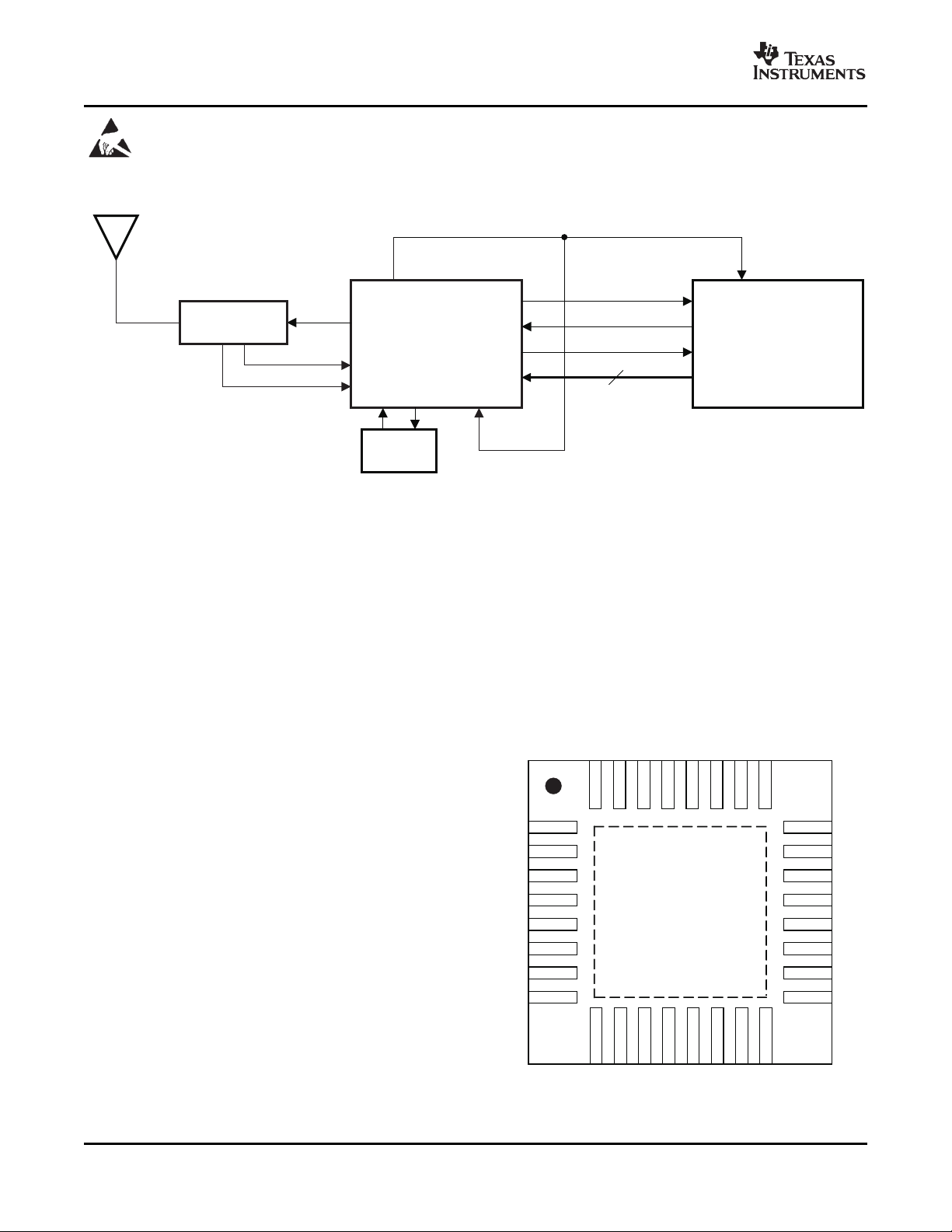
Figure 1. Typical Application
A parallel or serial interface can be used for The receiver system also includes a framing system.
communication between the MCU and reader. When This system performs the CRC and/or parity check,
hardware encoders and decoders are used removes the EOF and SOF settings, and organizes
(accelerators for different standards), transmission the data in bytes. Framed data is then accessible to
and receive functions use a 12-byte FIFO register. the MCU via a 12-byte FIFO register and MCU
For direct transmit or receive functions, the interface. The framing supports ISO14443 and
encoders/decoders can be bypassed in order for the ISO15693 protocols.
MCU to process the data in real time. The transmitter
has selectable output-power levels of 100 mW (20
dBm) or 200 mW (23 dBm) into a 50- Ω load (at 5 -V
supply) and is capable of ASK or OOK modulation.
Integrated voltage regulators ensure power-supply
noise rejection for the complete reader system.
The TRF7960/61 supports data communication
levels between 1.8 V–5.5 V for the MCU I/O interface
while also providing a data synchronization clock. An
auxiliary 20-mA regulator (pin 32) is available for
additional system circuits.
Data transmission comprises low-level encoding for
ISO15693, modified Miller for ISO14443-A,
high-bit-rate systems, Tag-it, and HF-EPC system
coding. Included with the data encoding is automatic
generation of SOF, EOF, CRC, and/or parity bits.
The receiver system enables AM and PM
demodulation using a dual-input architecture. The
receiver also includes an automatic gain control
Submit Documentation Feedback
Figure 2. TRF796x Pin Assignments (Top View)
option and selectable gain. Also included is a
selectable bandwidth to cover a broad range of input
subcarrier signal options. The received signal
strength for AM and PM modulation is accessible via
the RSSI register. The receiver output is selectable
between a digitized subcarrier signal and any of
eleven integrated subcarrier decoders (two for
ISO15693 low bit rate, two for ISO15693 high bit
rate, two for ISO14443, three for ISO14443 high bit
rates, one for Tag-it, and one for HF-EPC system).
Selected decoders also deliver bit stream and a data
clock as outputs.
2
www.ti.com
TRF7960/61
SLOS504B – AUGUST 2006 – REVISED APRIL 2007
ABSOLUTE MAXIMUM RATINGS
over operating free-air temperature range (unless otherwise noted)
VIN Supply voltage 6 V
I
O
T
J
T
stg
(1) The absolute maximum ratings under any condition is limited by the constraints of the silicon process. Stresses above these ratings may
(2) The maximum junction temperature for continuous operation is limited by package constraints. Operation above this temperature may
Output current 150 mA
Continuous power dissipation See Dissipation Rating Table
Maximum junction temperature, any condition
(2)
Maximum junction temperature, continuous operation, long-term reliability
Storage temperature range –55 to 150 ° C
Lead temperature 1,6 mm (1/16 inch) from case for 10 seconds 300 ° C
HBM (human body model) 2 kV
ESDS rating CDM (charged device model) 500
MM (machine model) 200
cause permanent damage. Exposure to absolute maximum conditions for extended periods may degrade device reliability. These are
stress ratings only and functional operation of the device at these or any other conditions beyond those specified are not implied.
result in reduced reliability and/or lifetime of the device.
(1)
VALUE UNIT
140 ° C
(2)
125 ° C
V
TABLE 5. PACKAGING/ORDERING INFORMATION
(1)
PACKAGED DEVICES PACKAGE TYPE TRANSPORT MEDIA QUANTITY
TRF7960RHBT Tape and reel 250
TRF7960RHBR Tape and reel 3000
TRF7961RHBT Tape and reel 250
TRF7961RHBR Tape and reel 3000
RHB-32
RHB-32
(1) For the most current package and ordering information, see the Package Option Addendum at the end of this document, or see the TI
Web site at www.ti.com .
DISSIPATION RATINGS TABLE PER PACKAGE
θ
PACKAGE
JC
( ° C/W) ( ° C/W)
(1)
θ
JA
TA≤ 25 ° C TA= 85 ° C
POWER RATING
RHB (32) 31 36.4 2.7 W 1.1 W
(1) This data was taken using the JEDEC standard high-K test PCB.
(2) Power rating is determined with a junction temperature of 125 ° C. This is the point where distortion starts to increase substantially.
Thermal management of the final PCB should strive to keep the junction temperature at or below 125 ° C for best performance and
long-term reliability.
(2)
RECOMMENDED OPERATING CONDITIONS
over operating free-air temperature range (unless otherwise noted)
MIN TYP MAX UNIT
VIN Supply voltage 2.7 5 5.5 V
T
J
T
A
Operating virtual junction temperature range –40 125 ° C
Operating ambient temperature range –40 25 110 ° C
Load impedance at TX OUT (pin 5) 10 Ω
Submit Documentation Feedback
3

PACKAGE OPTION ADDENDUM
www.ti.com
4-Apr-2007
PACKAGING INFORMATION
Orderable Device Status
(1)
Package
Type
Package
Drawing
Pins Package
Qty
Eco Plan
TRF7960RHBR ACTIVE QFN RHB 32 3000 Green (RoHS &
no Sb/Br)
TRF7960RHBT ACTIVE QFN RHB 32 250 Green (RoHS &
no Sb/Br)
TRF7961RHBR ACTIVE QFN RHB 32 3000 Green (RoHS &
no Sb/Br)
TRF7961RHBT ACTIVE QFN RHB 32 250 Green (RoHS &
no Sb/Br)
(1)
The marketing status values are defined as follows:
ACTIVE: Product device recommended for new designs.
LIFEBUY: TI has announced that the device will be discontinued, and a lifetime-buy period is in effect.
NRND: Not recommended for new designs. Device is in production to support existing customers, but TI does not recommend using this part in
a new design.
PREVIEW: Device has been announced but is not in production. Samples may or may not be available.
OBSOLETE: TI has discontinued the production of the device.
(2)
Eco Plan - The planned eco-friendly classification: Pb-Free (RoHS), Pb-Free (RoHS Exempt), or Green (RoHS & no Sb/Br) - please check
http://www.ti.com/productcontent for the latest availability information and additional product content details.
TBD: The Pb-Free/Green conversion plan has not been defined.
Pb-Free (RoHS): TI's terms "Lead-Free" or "Pb-Free" mean semiconductor products that are compatible with the current RoHS requirements
for all 6 substances, including the requirement that lead not exceed 0.1% by weight in homogeneous materials. Where designed to be soldered
at high temperatures, TI Pb-Free products are suitable for use in specified lead-free processes.
Pb-Free (RoHS Exempt): This component has a RoHS exemption for either 1) lead-based flip-chip solder bumps used between the die and
package, or 2) lead-based die adhesive used between the die and leadframe. The component is otherwise considered Pb-Free (RoHS
compatible) as defined above.
Green (RoHS & no Sb/Br): TI defines "Green" to mean Pb-Free (RoHS compatible), and free of Bromine (Br) and Antimony (Sb) based flame
retardants (Br or Sb do not exceed 0.1% by weight in homogeneous material)
(2)
Lead/Ball Finish MSL Peak Temp
CU NIPDAU Level-2-260C-1 YEAR
CU NIPDAU Level-2-260C-1 YEAR
CU NIPDAU Level-2-260C-1 YEAR
CU NIPDAU Level-2-260C-1 YEAR
(3)
(3)
MSL, Peak Temp. -- The Moisture Sensitivity Level rating according to the JEDEC industry standard classifications, and peak solder
temperature.
Important Information and Disclaimer:The information provided on this page represents TI's knowledge and belief as of the date that it is
provided. TI bases its knowledge and belief on information provided by third parties, and makes no representation or warranty as to the
accuracy of such information. Efforts are underway to better integrate information from third parties. TI has taken and continues to take
reasonable steps to provide representative and accurate information but may not have conducted destructive testing or chemical analysis on
incoming materials and chemicals. TI and TI suppliers consider certain information to be proprietary, and thus CAS numbers and other limited
information may not be available for release.
In no event shall TI's liability arising out of such information exceed the total purchase price of the TI part(s) at issue in this document sold by TI
to Customer on an annual basis.
Addendum-Page 1


IMPORTANT NOTICE
Texas Instruments Incorporated and its subsidiaries (TI) reserve the right to make corrections, modifications, enhancements,
improvements, and other changes to its products and services at any time and to discontinue any product or service without notice.
Customers should obtain the latest relevant information before placing orders and should verify that such information is current and
complete. All products are sold subject to TI’s terms and conditions of sale supplied at the time of order acknowledgment.
TI warrants performance of its hardware products to the specifications applicable at the time of sale in accordance with TI’s
standard warranty. Testing and other quality control techniques are used to the extent TI deems necessary to support this
warranty. Except where mandated by government requirements, testing of all parameters of each product is not necessarily
performed.
TI assumes no liability for applications assistance or customer product design. Customers are responsible for their products and
applications using TI components. To minimize the risks associated with customer products and applications, customers should
provide adequate design and operating safeguards.
TI does not warrant or represent that any license, either express or implied, is granted under any TI patent right, copyright, mask
work right, or other TI intellectual property right relating to any combination, machine, or process in which TI products or services
are used. Information published by TI regarding third-party products or services does not constitute a license from TI to use such
products or services or a warranty or endorsement thereof. Use of such information may require a license from a third party under
the patents or other intellectual property of the third party, or a license from TI under the patents or other intellectual property of TI.
Reproduction of information in TI data books or data sheets is permissible only if reproduction is without alteration and is
accompanied by all associated warranties, conditions, limitations, and notices. Reproduction of this information with alteration is an
unfair and deceptive business practice. TI is not responsible or liable for such altered documentation.
Resale of TI products or services with statements different from or beyond the parameters stated by TI for that product or service
voids all express and any implied warranties for the associated TI product or service and is an unfair and deceptive business
practice. TI is not responsible or liable for any such statements.
TI products are not authorized for use in safety-critical applications (such as life support) where a failure of the TI product would
reasonably be expected to cause severe personal injury or death, unless officers of the parties have executed an agreement
specifically governing such use. Buyers represent that they have all necessary expertise in the safety and regulatory ramifications
of their applications, and acknowledge and agree that they are solely responsible for all legal, regulatory and safety-related
requirements concerning their products and any use of TI products in such safety-critical applications, notwithstanding any
applications-related information or support that may be provided by TI. Further, Buyers must fully indemnify TI and its
representatives against any damages arising out of the use of TI products in such safety-critical applications.
TI products are neither designed nor intended for use in military/aerospace applications or environments unless the TI products are
specifically designated by TI as military-grade or "enhanced plastic." Only products designated by TI as military-grade meet military
specifications. Buyers acknowledge and agree that any such use of TI products which TI has not designated as military-grade is
solely at the Buyer's risk, and that they are solely responsible for compliance with all legal and regulatory requirements in
connection with such use.
TI products are neither designed nor intended for use in automotive applications or environments unless the specific TI products
are designated by TI as compliant with ISO/TS 16949 requirements. Buyers acknowledge and agree that, if they use any
non-designated products in automotive applications, TI will not be responsible for any failure to meet such requirements.
Following are URLs where you can obtain information on other Texas Instruments products and application solutions:
Products Applications
Amplifiers amplifier.ti.com Audio www.ti.com/audio
Data Converters dataconverter.ti.com Automotive www.ti.com/automotive
DSP dsp.ti.com Broadband www.ti.com/broadband
Interface interface.ti.com Digital Control www.ti.com/digitalcontrol
Logic logic.ti.com Military www.ti.com/military
Power Mgmt power.ti.com Optical Networking www.ti.com/opticalnetwork
Microcontrollers microcontroller.ti.com Security www.ti.com/security
Low Power www.ti.com/lpw Telephony www.ti.com/telephony
Wireless
Video & Imaging www.ti.com/video
Wireless www.ti.com/wireless
Mailing Address: Texas Instruments, Post Office Box 655303, Dallas, Texas 75265
Copyright © 2007, Texas Instruments Incorporated
 Loading...