

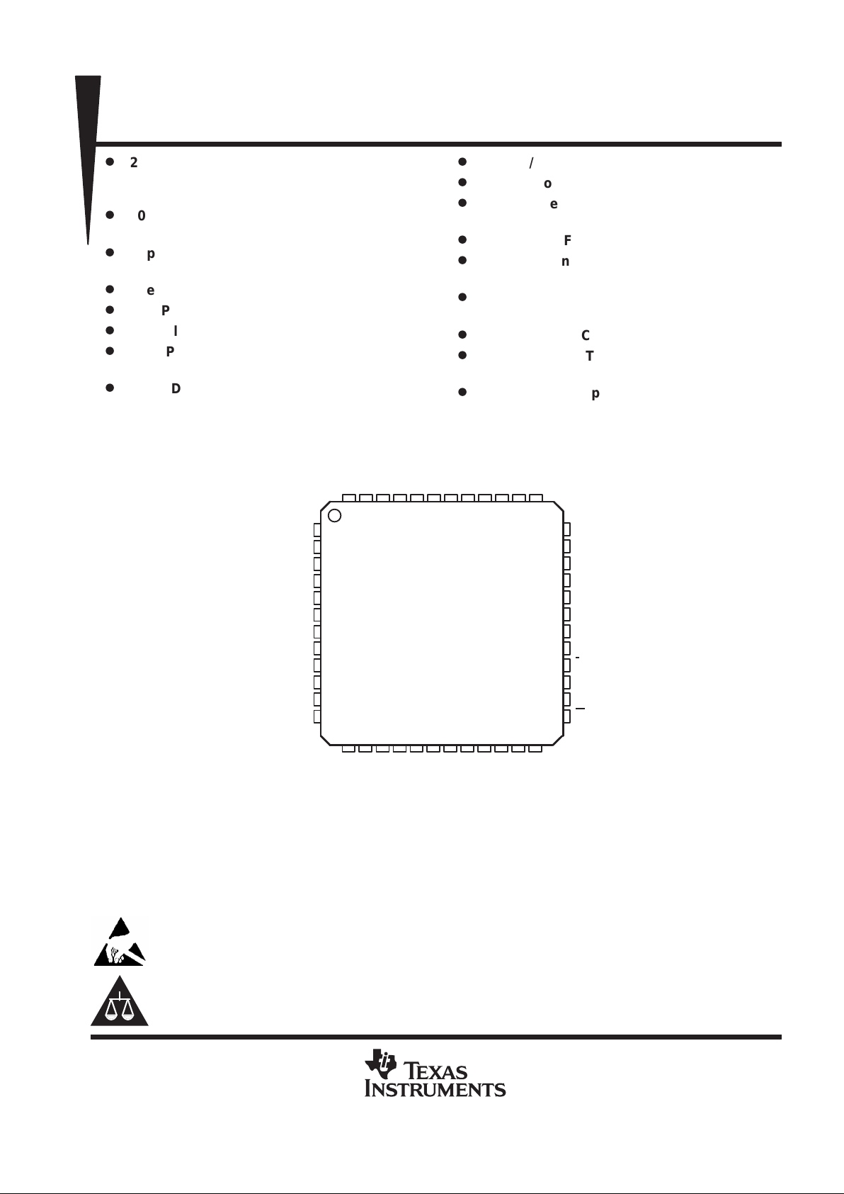
TRF3040
MODULATOR/SYNTHESIZER
SLWS057 – AUGUST 1999
1
POST OFFICE BOX 655303 • DALLAS, TEXAS 75265
D
2-GHz Main Synthesizer, Which
Incorporates a Dual-Mode 32/33 and 64/65
Prescaler for Fractional-N Operation
D
200-MHz Auxiliary Synthesizer, Which
Incorporates an 8/9 Prescaler
D
Separate Supply Terminals for Main and
Auxiliary Charge Pumps
D
Internal Compensation for Fractional Spurs
D
Low Phase Noise
D
Normal and Integral Charge Pump Outputs
D
Fully Programmable Main and Auxiliary
Dividers
D
Serial Data Interface
D
Direct I/Q Modulator
D
Control Logic for Power-Down Modes
D
Single-Sideband Suppressed Carrier
(SSBSC) Converter to Generate TX Carrier
D
200-MHz TXIF Synthesizer and Oscillator
D
Variable Gain Amplifier (VGA) W ith 50 dB of
Dynamic Range
D
900-MHz Power Amplifier (P A) Driver With
9 dBm Typical Output Power
D
Reference and Clock Buffers
D
158 mA Typical Total Operating Current at
3.75 V Supply
D
48-Pin Quad Flatpack (LQFP)
14 15
XTAL–
TXEN
DATA
CLOCK
LOCK
STROBE
V
SSA
V
DD
I
I
Q
Q
36
35
34
33
32
31
30
29
28
27
26
25
16
1
2
3
4
5
6
7
8
9
10
11
12
PHP
V
DDA
RXLO+
RXLO–
V
SSA
V
CCP
TXLO+
TXLO–
V
SSP
PHSOUT
IPEAK
TANK+
17 18 19 20
PHA
RCLK
MCLK
47 46 45 44 4348 42
PHIRFRN
V
GND
40 39 3841
21
22 23 24
37
13
INA
RA
TANK–
V
DDA
DUALTX+
DUALTX–
V
DDA
V
DDA
V
DDA
XTAL+
PT PACKAGE
(TOP VIEW)
SS
V
SSAVSSAVSSAVSSAVSSAVSSA
These devices have limited built-in ESD protection. The leads should be shorted together or the device placed in conductive foam
during storage or handling to prevent electrostatic damage to the MOS gates.
Please be aware that an important notice concerning availability, standard warranty, and use in critical applications of
Texas Instruments semiconductor products and disclaimers thereto appears at the end of this data sheet.
PRODUCTION DATA information is current as of publication date.
Products conform to specifications per the terms of Texas Instruments
standard warranty. Production processing does not necessarily include
testing of all parameters.
Copyright 1999, Texas Instruments Incorporated

TRF3040
MODULATOR/SYNTHESIZER
SLWS057 – AUGUST 1999
2
POST OFFICE BOX 655303 • DALLAS, TEXAS 75265
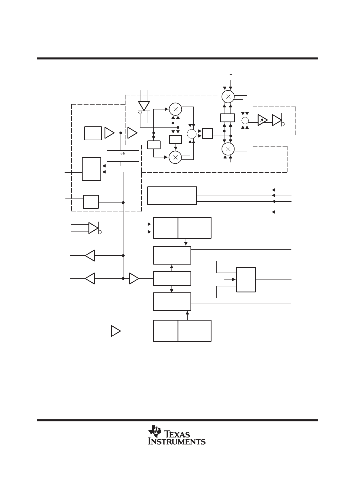
description
The TRF3040 is an integrated transmit modulator/synthesizer circuit suitable for 900-MHz analog and digital
cellular telephones. It consists of a transmit intermediate frequency (TXIF) synthesizer and oscillator, a
single-sideband suppressed carrier (SSBSC) converter , a direct conversion I/Q modulator , a variable gain
amplifier (VGA) with a power amplifier (PA) driver, a main channel fractional-N synthesizer, an auxiliary
channel synthesizer, a crystal oscillator reference buffer, and clock buffers in a small surface-mount
package. Very few external components are required.
The TXIF synthesizer produces the offset signal, TXIF, needed to translate the external local oscillator
(TXLO) signal to the correct transmission frequency. The TXIF_VCO (voltage controlled oscillator) can
operate from 90 MHz to 200 MHz, depending on the component values chosen for the external tank circuit.
The TXLO signal may be differential or single-ended input.
The direct conversion I/Q modulator places the modulation signal (π/4-DQPSK, FM) directly on top of the
transmit carrier frequency.
The VGA has an output range of –41 dBm to 9 dBm into a 200-Ω differential load. The balanced output signal
simplifies the board layout making it easier to meet isolation requirements.
TRF3040
MODULATOR/SYNTHESIZER
SLWS057 – AUGUST 1999
3
POST OFFICE BOX 655303 • DALLAS, TEXAS 75265
functional block diagram
TXIF_
VCO
N
(N = 6, 7, 8, 9)
TXIF
TXIF_LD
+90
+90
+
+
+90
Σ
Control Logic
Main
Prescaler
÷ 32/33
Main Phase
Detector
Reference
Divider
Auxiliary
Phase Detector
Auxiliary
Divider
Lock
Detect
TXLO +
DUALTX+
I
TXEN
DATA
CLOCK
STROBE
PHP
PHI
LOCK
PHA
+
–
RXLO
MCLK
RCLK
INA
TXIF_LD
DUALTX–
TANK+
TANK–
PHSOUT
Σ
+
+
12
13
IPEAK
10
11
3
4
38
39
37
43
26
8
7
25
20
22
28
27
35
34
33
31
1
48
32
41
36
INR
Q
Q
–
XTAL
XTAL
XTAL
OSC
I
+
–
RCLK Buffer
Main Divider
Main
Prescaler
÷ 8/9
Auxiliary Synthesizer
Input Buffer
Reference
Divider Buffer
MCLK Buffer
RXLO Buffer
TXIF
Phase
Detector
and
Charge
Pump
TXIF_VCO
Buffer
TXIF_Buffer
TXLO –
BPF
DUALTX
VGA
I/Q Modulator
Transmit Intermediate
Frequency Synthesizer
SSBSC Converter and TXIF Buffer
TXLO_Buffer
TXRF
PA Driver
TRF3040
MODULATOR/SYNTHESIZER
SLWS057 – AUGUST 1999
4
POST OFFICE BOX 655303 • DALLAS, TEXAS 75265
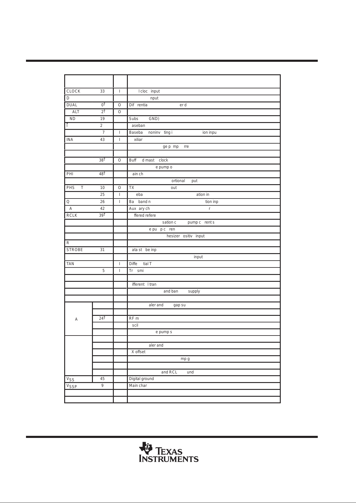
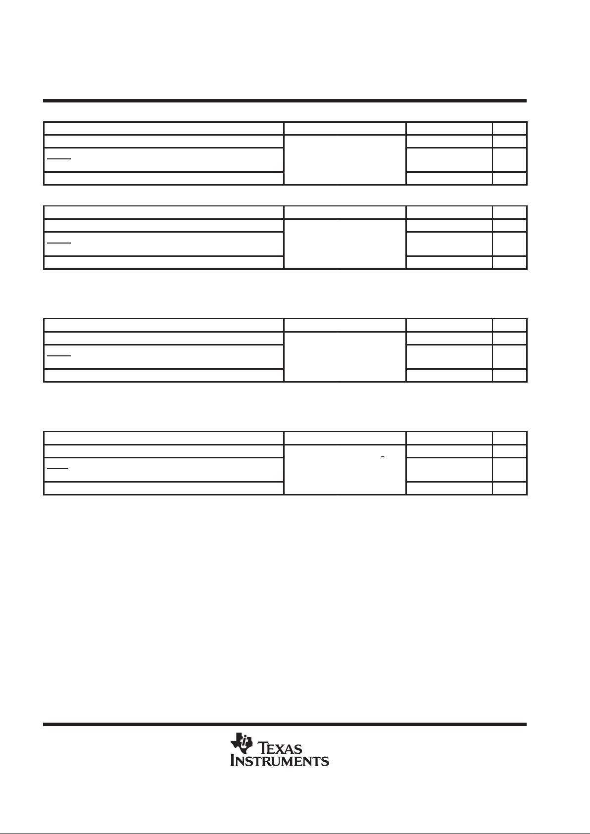
Terminal Functions
TERMINAL
NAME NO.
I/O
DESCRIPTION
CLOCK
33
I Serial clock input
DATA
34
I Serial data input
DUALTX+
20
†
O Differential RF power amplifier driver
DUALTX–
22
†
O Differential RF power amplifier driver
GND
19
Substrate (GND)
I
28
I Baseband inverting in-phase modulation input
I
27
I Baseband noninverting in-phase modulation input
INA
43
I Auxiliary synthesizer input
IPEAK
11
TX offset loop charge pump current setting resistor
LOCK
32
O Lock detect output
MCLK
38
†
O Buffered master clock output
PHA
41
O Auxiliary charge pump output
PHI
48
†
O Main charge pump integral output
PHP
1
O Main charge pump proportional output
PHSOUT
10
O TX offset charge pump output
Q
25
I Baseband inverting quadrature modulation input
Q
26
I Baseband noninverting quadrature modulation input
RA
42
Auxiliary charge pump current setting resistor
RCLK
39
†
O Buffered reference clock output
RF
47 Fractional compensation charge pump current setting resistor
RN
46 Main charge pump current setting resistor
RXLO+
3 I Differential main synthesizer positive input
RXLO–
4 I Differential main synthesizer negative input
STROBE 31 I Data strobe input
TANK+ 12 I Differential TXIF_VCO tank positive input
TANK– 13 I Differential TXIF_VCO tank negative input
TXEN 35 I Transmit enable
TXLO+ 7 I Differential transmit LO positive input
TXLO– 8 I Differential transmit LO negative input
V
CCP
6
Main charge pump and bandgap supply voltage
V
DD
29 Digital supply voltage
2 Main prescaler and bandgap supply voltage
14 TX offset loop supply voltage
V
DDA
24
†
RF modulator supply voltage
40 Oscillator and buffers supply voltage
44 Auxiliary charge pump supply voltage
17, 18 RF modulator ground
5 Main prescaler and bandgap ground
15 TX offset loop ground
V
SSA
16 TX offset loop and charge pump ground
21, 23 PA driver ground
30 Oscillator, MCLK, and RCLK ground
V
SS
45 Digital ground
V
SSP
9 Main charge pump ground
XTAL+ 37 I Crystal oscillator base input
XTAL– 36 O Crystal oscillator emitter input
†
Pins have limited ESD protection
TRF3040
MODULATOR/SYNTHESIZER
SLWS057 – AUGUST 1999
5
POST OFFICE BOX 655303 • DALLAS, TEXAS 75265
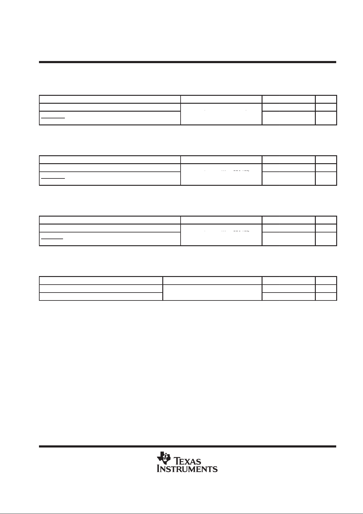
absolute maximum ratings over operating free-air temperature range (unless otherwise noted)
†
Power supply voltage range , V
CCP
, V
DD,
V
DDA
(see Note 1) –0.3 V to 4.5 V. . . . . . . . . . . . . . . . . . . . . . . . . . .
Voltage applied to any other terminal, VIN –0.3 V to VCC/V
DD
+ 0.3 V. . . . . . . . . . . . . . . . . . . . . . . . . . . . . . . . .
Operation junction temperature, T
Jmax
150°C. . . . . . . . . . . . . . . . . . . . . . . . . . . . . . . . . . . . . . . . . . . . . . . . . . . . .
Operating temperature, T
A
–40°C to 85°C. . . . . . . . . . . . . . . . . . . . . . . . . . . . . . . . . . . . . . . . . . . . . . . . . . . . . . . . .
Storage temperature, T
stg
–65°C to 150°C. . . . . . . . . . . . . . . . . . . . . . . . . . . . . . . . . . . . . . . . . . . . . . . . . . . . . . . . .
†
Stresses beyond those listed under “absolute maximum ratings” may cause permanent damage to the device. These are stress ratings only, and
functional operation of the device, at these or any other conditions beyond those indicated under “recommended operating conditions”, is not
implied. Exposure to absolute-maximum-rated conditions for extended periods may affect device reliability .
NOTE 1: Voltage values are in respect to V
SSA
(V
SSA
= V
SSP
= VSS = GND)
recommended operating conditions
PARAMETER
MIN NOM MAX UNIT
Supply voltage, V
CCP
, VDD, V
DDA
3.6 3.75 3.9 V
High-level input voltage, VIH (CLOCK, DATA, STROBE, TXEN) 0.7×V
DD
VDD+0.3 V
Low-level input voltage, VIL (CLOCK, DATA, STROBE, TXEN) –0.3 0.3×V
DD
V
Main synthesizer input frequency, f
IN(RXLO±)
2000 MHz
Main synthesizer input power, P
IN(RXLO±)
, (AC coupled, 50-Ω single ended, 100-Ω differential) –17 dBm
Transmit LO input frequency, f
IN(TXLO±)
1050 MHz
Transmit LO input power , P
IN(TXLO±)
, (AC coupled, 50-Ω single ended, 100-Ω differential) –10 dBm
TXIF_VCO tank differential input frequency, f
IN(TANK±)
200 MHz
Crystal oscillator input frequency, f
IN(XTAL+)
25 MHz
Auxiliary synthesizer input frequency, f
IN(INA)
200 MHz
Auxiliary synthesizer input voltage, V
IN(INA)
, (AC coupled) 0.2 V
PP
In-phase differential input, I/I (quiescent) V
DDA
/2 V
Quadraphase differential input, Q/Q (quiescent) V
DDA
/2 V
Operating free-air temperature, T
A
–40 25 85 °C
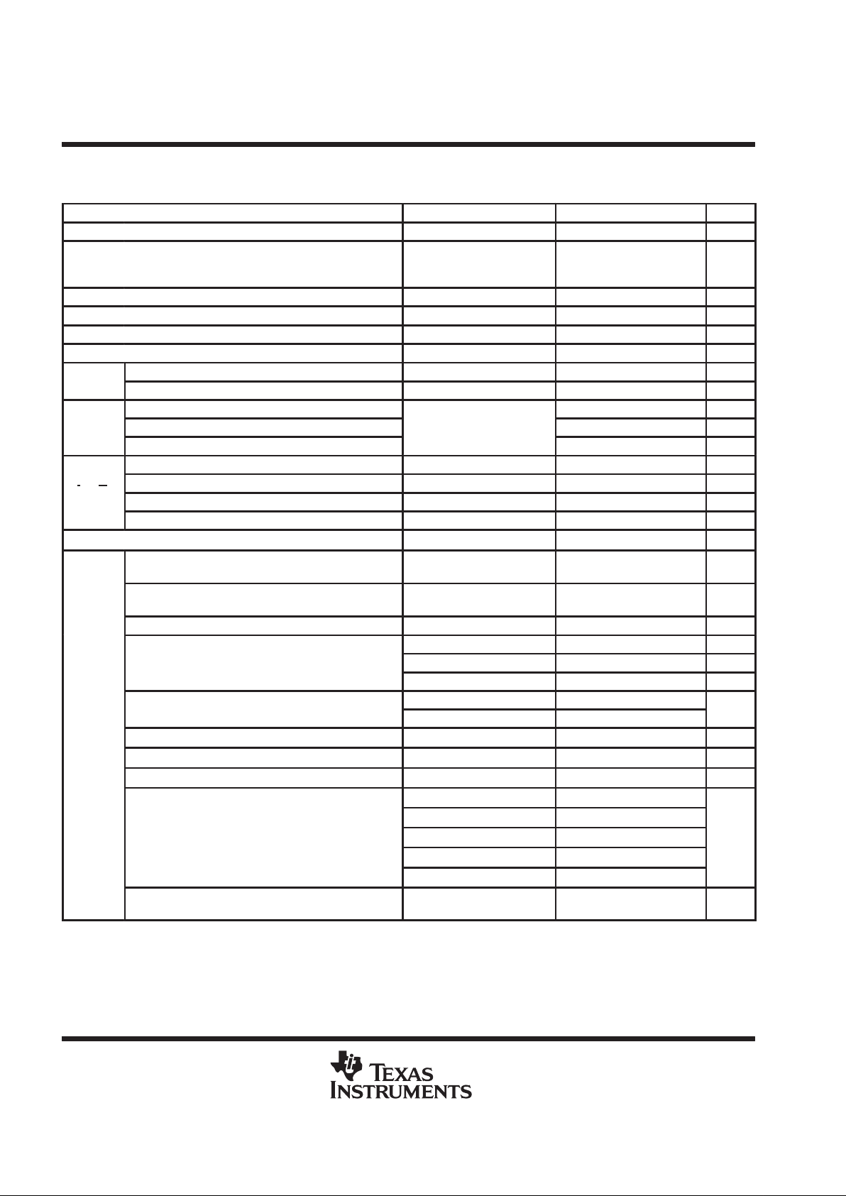
dc electrical characteristics V
CCP
= VDD = V
DDA
= 3.75 V, TA = 25°C (unless otherwise noted)
supply current I = I
CCP
+ IDD + I
DDA
PARAMETER TEST CONDITIONS
MIN TYP MAX UNIT
I
SLEEP
Sleep mode supply current 2 3 mA
I
STANDBY
Standby mode supply current 22 mA
I
OPER_ANA
Operating supply current – full power analog mode (MODE=0) 142 mA
I
OPER_DIG
Operating supply current – full power digital mode (MODE=1) 158 mA
dc electrical characteristics V
CCP
= VDD = V
DDA
= 3.75 V, TA = 25°C (unless otherwise noted)
(continued)
digital interface
PARAMETER TEST CONDITIONS
MIN TYP MAX UNIT
p
IO = 1 µA 0.050 V
VOLOutput voltage, lo
w
IO = 2 mA
0.4 V
p
IO = –1 µA VDD – 0.050 V
VOHOutput voltage, high
IO = –2 mA VDD – 0.4 V
TRF3040
MODULATOR/SYNTHESIZER
SLWS057 – AUGUST 1999
6
POST OFFICE BOX 655303 • DALLAS, TEXAS 75265
charge pump PHA
PARAMETER TEST CONDITIONS
MIN TYP MAX UNIT
I
PHA
Output current at PHA 200 250 300 µA
∆I
PHA
I
PHA
Relative output current variation (see Figure 1)
RA = 100 kΩ, V
PHA
= V
DDA
/2
2% 10%
∆I
PHA
Output current matching PHA (see Figure 1) 10%
charge pump PHP, normal mode, VRF = V
DDA
(see Note 2)
PARAMETER TEST CONDITIONS
MIN TYP MAX UNIT
I
PHP
Output current at PHP ±250 ±288 ±320 µA
∆I
PHP
I
PHP
Relative output current variation (see Figure 1)
CN = 128,
RN = 120 kΩ
V
PHP = VDDA/2
,
2% 10%
∆I
PHP
Output current matching PHP (see Figure 1) 10%
NOTE 2: When a serial input word A is programmed, the main charge pump on the PHP and PHI is in the speed-up mode as long as
STROBE is high in standard programming or until the speed-up mode counter reaches its terminal count. When this is not the case,
the main charge pumps are in normal mode.
charge pump PHP, speed-up mode, VRF = V
DDA
(see Note 2)
PARAMETER TEST CONDITIONS
MIN TYP MAX UNIT
I
PHP
Output current at PHP ±1.2 ±1.6 ±1.9 mA
∆I
PHP
I
PHP
Relative output current variation (see Figure 1)
CN = 128,
RN = 120 kΩ
V
PHP
= V
DDA/2
,
2% 10%
∆I
PHP
Output current matching PHP (see Figure 1) 10%
NOTE 2: When a serial input word A is programmed, the main charge pump on the PHP and PHI is in the speed-up mode as long as
STROBE is high in standard programming or until the speed-up mode counter reaches its terminal count. When this is not the case,
the main charge pumps are in normal mode.
charge pump PHI, speed-up mode, VRF = V
DDA
(see Note 2)
PARAMETER TEST CONDITIONS
MIN TYP MAX UNIT
I
PHI
Output current at PHI
±3.3 ±4 ±4.5 mA
∆I
PHI
I
PHI
Relative output current variation (see Figure 1)
CN = 128,
CK = 3,
C
L = 1
RN = 120 kΩ,
V
PHA
= V
DDA
/2,
2% 10%
∆I
PHI
Output current matching PHI (see Figure 1)
CL = 1
10%
NOTE 2: When a serial input word A is programmed, the main charge pump on the PHP and PHI is in the speed-up mode as long as
STROBE is high in standard programming or until the speed-up mode counter reaches its terminal count. When this is not the case,
the main charge pumps are in normal mode.
TRF3040
MODULATOR/SYNTHESIZER
SLWS057 – AUGUST 1999
7
POST OFFICE BOX 655303 • DALLAS, TEXAS 75265
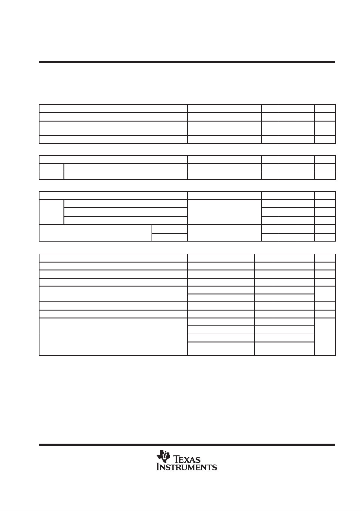
dc electrical characteristics V
CCP
= VDD = V
DDA
= 3.75 V, TA = 25°C (unless otherwise noted)
(continued)
fractional compensation PHP, normal mode, VRN = V
DDA
(see Note 2)
PARAMETER TEST CONDITIONS
MIN TYP MAX UNIT
I
PHP–FR
Output current PHP vs. fractional numerator
FMOD = 1, RF = 120 kΩ,
–340 –270 –170 nA
∆I
PHP–FR
I
PHP–FR
Relative output current (see Figure 1)
,
CN = 128,
CK = 3,
,
V
PHP
= V
DDA/2
,
CL = 1
10%
NOTE 2: When a serial input word A is programmed, the main charge pump on the PHP and PHI is in the speed-up mode as long as STROBE
is high in standard programming or until the speed-up mode counter reaches its terminal count. When this is not the case, the main
charge pumps are in normal mode.
fractional compensation PHP, speed-up mode, VRN = V
DDA
(see Note 2)
PARAMETER TEST CONDITIONS
MIN TYP MAX UNIT
I
PHP–FR
Output current PHP vs. fractional numerator
FMOD = 1,
RF = 120 kΩ
,
–1.7 –1.4 –1.1 µA
∆I
PHP–FR
I
PHP–FR
Relative output current (see Figure 1)
,
CN = 128,
CK = 3,
RF 120 kΩ,
V
PHP
=V
DDA/2
,
CL = 1
15%
NOTE 2: When a serial input word A is programmed, the main charge pump on the PHP and PHI is in the speed-up mode as long as STROBE
is high in standard programming or until the speed-up mode counter reaches its terminal count. When this is not the case, the main
charge pumps are in normal mode.
fractional compensation PHI, speed-up mode, VRN = V
DDA
(see Note 2)
PARAMETER TEST CONDITIONS
MIN TYP MAX UNIT
I
PHI–FR
Output current PHI vs. fractional numerator
FMOD = 1,
RF = 120 kΩ
,
–5.1 –4 –2.9 µA
∆I
PHI–FR
I
PHI–FR
Relative output current (see Figure 1)
,
CN = 128,
CK = 3,
RF 120 kΩ,
V
PHI
= V
DDA/2
,
CL = 1
15%
NOTE 2: When a serial input word A is programmed, the main charge pump on the PHP and PHI is in the speed-up mode as long as STROBE
is high in standard programming or until the speed-up mode counter reaches its terminal count. When this is not the case, the main
charge pumps are in normal mode.
charge pump leakage currents
PARAMETER TEST CONDITIONS
MIN TYP MAX UNIT
I
PHI
Output leakage current PHI
±0.1 ±10 nA
I
PHA
Output leakage current PHA
V
RF
=
V
RN
=
V
DDA
,
V
PHP
= 0 to
V
DDA
±0.1 ±10 nA
TRF3040
MODULATOR/SYNTHESIZER
SLWS057 – AUGUST 1999
8
POST OFFICE BOX 655303 • DALLAS, TEXAS 75265
ac electrical characteristics V
CCP
= VDD = V
DDA
= 3.75 V, TA = 25°C (unless otherwise noted)
transmit intermediate frequency synthesizer, SSBSC converter and I/Q modulator
PARAMETER TEST CONDITIONS MIN TYP MAX UNIT
TXLO± Transmit LO input frequency 900 1100 MHz
TXLO± Transmit LO input power
AC coupled;
50-Ω single-ended,
100-Ω differential
–13 –10 dBm
TANK± TXIF_VCO tank differential input frequency range 155 MHz
PHSOUT TXIF_PD charge pump output level 0.5 V
DDA
–0.5 V
IPEAK TXIF_PD charge pump current setting R
IPEAK
= 13 kΩ 2.3 mA
Kφ TXIF_PD phase gain PLL in phase lock 1.46 mA/rad
XTAL oscillator input frequency 15 25 MHz
XTAL
+
XTAL negative resistance With external capacitors –100 Ω
Frequency range 20 MHz
RCLK,
Output levels
RCLK, MCLK load circuit
0.7 1 1.4 V
PP
MCLK
Harmonic content 10 dBc
Differential input frequency 1.8 MHz
Differential modulation level 0.8 0.9 1.0 V
PEAK
I/I, Q/Q
Differential input impedance 10 kΩ
DC bias point 1.65 1.7 2.0 V
TXRF TX operating frequency range 820 920 MHz
RF output frequency
SE = 1, TXEN = 1,
AMPS/DAMPS
820 853 MHz
Output power (I/Q set to typical conditions)
Open collector, matched to
200 Ω differential impedance
9 dBm
Gain flatness 1 dB
3rd order 33 36 dBc
Linearity in DAMPS mode (I/Q in phase, levels set to
5th order 45 62 dBc
nominal conditions Pout set to 8 dBm)
7th order 53 70 dBc
pp
VGA set to Pout = 8 dBm 26 40
Carrier suppression, I & Q in quadrature
VGA set to Pout = –38 dBm 33
dBc
DUALTX±
Sideband suppression, I & Q in quadrature 25 43 dBc
Adjacent channel noise power Ar 30 kHz offset –95 dBc/Hz
Alternate channel noise power At 60 kHz offset –101 dBc/Hz
TXLO 21 33
Upper sideband 21 60
TXLO conversion products (see Note 3)
TXLO –2×TXIF 15
dBc
TXLO ±3×TXIF 36
Harmonics ≤ 10th 21
Broadband noise (0-dB VGA or 9-dBm output,
whichever is less
869 to 894 MHz –124 dBc/Hz
NOTE 3: Parameters may vary depending on external output matching circuit.
TRF3040
MODULATOR/SYNTHESIZER
SLWS057 – AUGUST 1999
9
POST OFFICE BOX 655303 • DALLAS, TEXAS 75265
ac electrical characteristics V
CCP
= VDD = V
DDA
= 3.75 V, TA = 25°C (unless otherwise noted)
(continued)
frequency synthesizers
main divider
PARAMETER TEST CONDITIONS MIN TYP MAX UNIT
RXLO± Main synthesizer input frequency 2000 MHz
RXLO± Main synthesizer input power
AC coupled, external shunt 50-Ω
single-ended, 100 Ω differential
–17 dBm
RXLO± Main synthesizer input harmonics and subharmonics No multiclocking 30 dBc
reference divider
PARAMETER TEST CONDITIONS MIN TYP MAX UNIT
Operating frequency 25 MHz
INR
Harmonics No multiclocking 10 dBc
auxiliary divider
PARAMETER TEST CONDITIONS MIN TYP MAX UNIT
Auxiliary synthesizer input frequency 110 MHz
INA
Auxiliary synthesizer input signal amplitude
No multiclocking
0.2 V
PP
Auxiliary synthesizer input harmonics 10 dBc
p
p
Resistance 5 100 kΩ
Z
INA
Auxiliary synthesizer in ut im edance
Capacitance 3 pF
timing requirements, serial data interface (see Figure 6)
PARAMETER TEST CONDITIONS MIN TYP MAX UNIT
DATA Serial data input rate 10 MHz
CLOCK Serial data clock input 10 MHz
STROBE Serial data strobe input 10
Transmit enable TXEN=1
TXEN
Transmit enable
Transmit disable TXEN=0
Logic
t
su
Setup time: Data to CLOCK, CLOCK to STROBE 30 ns
t
k
Hold time. CLOCK to DATA 30 ns
CLOCK 30
STROBE (B-G words) 100
t
sw
Pulse width
A-word, PR = 01
1/f
VCO
× (NM2 × 65) + t
w
ns
A-word, PR = 10
1/f
VCO
× (NM2 × 65) +
(NM3+1) × 72) + t
w
TRF3040
MODULATOR/SYNTHESIZER
SLWS057 – AUGUST 1999
10
POST OFFICE BOX 655303 • DALLAS, TEXAS 75265
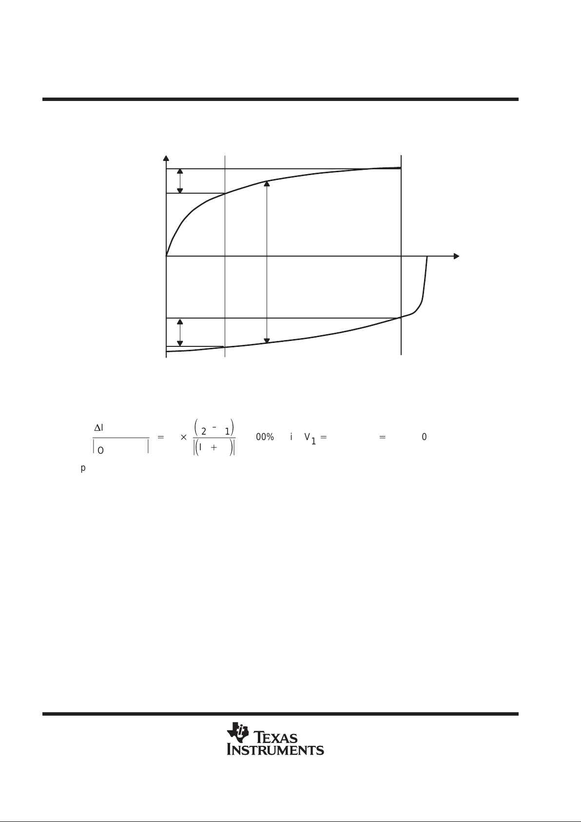
PARAMETER MEASUREMENT INFORMATION
charge-pump current output definitions
I
2
I
1
I
2
I
1
Current
Voltage
∆ I
OUT
REL
∆ I
OUT
MATCH
I
SINK
I
SOURCE
∆ I
OUT
REL
V
1
V
2
Figure 1. Charge-Pump Output Current Definitions
The relative output current variation is defined as the percent difference between charge-pump current output
at two charge-pump output voltages and the mean charge-pump current output (see Figure 1):
D
I
OUT REL
Ť
I
OUT MEAN
Ť
+2
ǒ
I2–I
1
Ǔ
Ť
ǒ
I2)
I
1
Ǔ
Ť
× 100%; with V1+
0.7 V, V2+
V
DDA
–0.8 V.
Output current matching is defined as the difference between charge-pump sinking current output and
charge-pump sourcing current output at a given charge-pump output (see Figure 1).
∆I
OUT MATCH
= I
SINK
– I
SOURCE
; with V1 ≤ Voltage ≤ V2.
TRF3040
MODULATOR/SYNTHESIZER
SLWS057 – AUGUST 1999
11
POST OFFICE BOX 655303 • DALLAS, TEXAS 75265
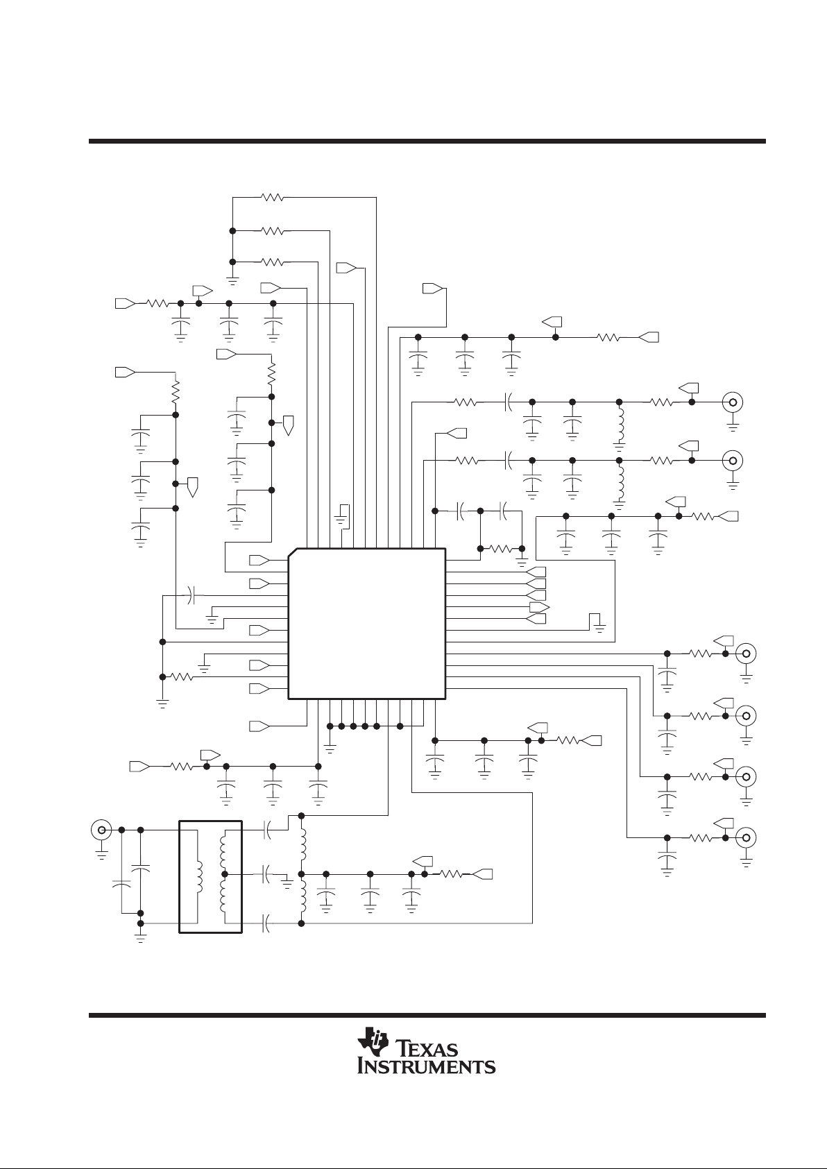
APPLICATION INFORMATION
2
3
4
5
6
7
8
9
10
11
12
1
35
34
33
32
31
30
29
28
27
26
25
36
23
22
21
20
19
18
17
16
15
14
13
24
38
39
40
41
42
43
44
45
46
47
48
37
C1
27pFC2.01µF
C3
15µF
R1
10
VCC
OSC_VCC
R4
9.1k
Ω
C4
.01µF
C5
15pF
C50
15pF
R6
4.7kΩ
RCLK
J1
L1
2200nH
XTAL
R8
9.1kΩ
C6
.01µF
C7
15pF
C71
15pF
R9
4.7kΩ
MCLK
J2
L2
2200nH
C11
DNP
C12
DNP
R11
DNP
TXEN
DATA
CLOCK
LOCK
STROBE
C13
27pF
C14
.01µF
C15
15µF
R12
10
VCC
D_VCC
R13
0
1–
J3
U1
TRF3040
C21
DNP
R15
0
1
J4
C22
DNP
R18
0
Q
J5
C29
DNP
R19
0
Q–
J7
C31
DNP
C23
27pF
C24 C25
.01 µF
R16
0
VCC
RF_VCC
C28
27pF
C27
.01µF
C26
TANK–
PD_VCC
R17
0
VCC
DUALTX
C34
27pF
C98
15 µF
C99
.01µF
R57
0
VCC
PA_VCC
L3
12nH
L4
12nH
DUALTX–
C30
2.2pF
C33
10pF
C35
2.2pF
BALUN1
SLT–090G
1
3
4
6
5
C32
1.8pF
J6
TANK
PHSOUT
R14
18kΩ
PHP
RXLO
TXLO
C97
27pF
C101
.01µF
C104
15µF
R23
10
VCC
AUX_VCC
PHI
R7
120kΩ
R3
33kΩ
R2
100kΩ
PHA
C10
27pF
C9
.01µF
C8
15µF
P_VCC
R10
10
VCC
C19
27pF
C18
.01µF
C17
15µF
CP_VCC
R5
10
VCC
INA
15µF
+
+
+
+
+
+
+
+
Note: DNP = Do Not Place
C16
22pF
C111
3.3pF
15 µF
Figure 2. Evaluation Board Schematic
TRF3040
MODULATOR/SYNTHESIZER
SLWS057 – AUGUST 1999
12
POST OFFICE BOX 655303 • DALLAS, TEXAS 75265
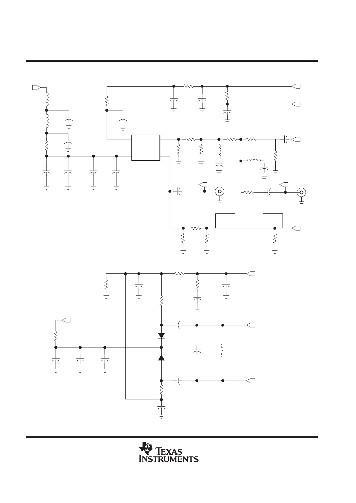
APPLICATION INFORMATION
L10
12nH
MVCO
RTL402672
M/CO__VCC
PHP
TXLO
+
PHI
RXLO
+
C102
27pF
L11
12nH
R24
10
C45
100µF
C103
27pF
C46
.01µF
C47
DNP
C107
27pF
(100µF)
VT
VVCO2X1X
2X7
11X
5
8
R20
1.5kΩ
C36
470pF
R21
3.9kΩ
C37
1500pF
C38
1500pF
R22
5.1kΩ
C39
.022µF
TXLO
R43
30
R25
18
R30
18
R42
180
R40
180
L12
5.6nH
C49
4.7pF
R26
18
L13
1.5nH
C51
1pF
R28
49.9
C42
22pF
C48
22pF
J8
STRIPLINE
J9C55
DNP
9dB ATTENUATOR
PAD
R27
62
R29
100
R31
100
R32
49.9
RXLO
9
5dB ATTENUATOR
PAD
+
MAIN VCO
R61
10 MΩ
C56
100 pF
NET00033
R37
1 kΩ
R39
1 kΩ
C65
100 pF
C63
27 pF
C62
.01 µF
C61
1 µF
R38
1 kΩ
V
CC
1
3
2
3
VC1:A
KV1470
VC1:B
KV1470
C60
3 pF
L9
82 nH
TANK+
TANK–
PHSOUT
C57
330 pF
C58
3300 pF
R36
360 Ω
R35
51 kΩ
C59
33 pF
C64
33 pF
+
TANK CKT
Ω
Ω
Ω
ΩΩ
Ω
Ω
Ω
Ω
Ω
Figure 2. Evaluation Board Schematic (continued)

TRF3040
MODULATOR/SYNTHESIZER
SLWS057 – AUGUST 1999
13
POST OFFICE BOX 655303 • DALLAS, TEXAS 75265
APPLICATION INFORMATION
C69
1 µF
C68
.01 µF
C67
27 pF
R41
10 Ω
TCXO_V
CC
TCO-980
TOYOCOM
TCXO
C70
0.1 µF
+
C66
.01 µF
J10
V
CC
VCONT
OUT
GND
4
1
3
2
XTAL
REF_IN
C81
1 µF
C80
.01 µF
C79
27 pF
R47
10 Ω
AVCO_V
CC
VCO190-S
VARIL
AVCO
C82
0.1 µF
+
C78
.022 µF
J11
V
CC
MOD
OUT
VT
14
6
10
2
INA
AUX_OUT
C77
.022 µF
R49
18 Ω
R50
49.9 Ω
R48
18 Ω
PHA
R52
0 Ω
R53
6.2 kΩ
R51
1.5 kΩ
C86
0.015 pF
C84
470 pF
C85
DNP
C83
1000 pF
R46
18 Ω
AUXILIARY VCO & REFERENCE TCX0
Figure 2. Evaluation Board Schematic (continued)

TRF3040
MODULATOR/SYNTHESIZER
SLWS057 – AUGUST 1999
14
POST OFFICE BOX 655303 • DALLAS, TEXAS 75265
APPLICATION INFORMATION
LM317LD
VR1
NC
VO
VI
VO
8
7
1
2
VO
NC
VO
ADJ
6
5
3
4
OPTO_V
CC
R55
220 Ω
C88
1 µF
+
1
OPTO_VCC_TP
3.75 V
SETTING
W
CCW
CW
R59
1 kΩ
LM317LD
VR2
NC
VO
VI
VO
8
7
1
2
VO
NC
VO
ADJ
6
5
3
4
5 V
R56
220 Ω
C89
1 µF
+
1
5V_TP
5 V
SETTING
W
CCW
CW
R60
1 kΩ
LM317LD
VR5
NC
VO
VI
VO
8
7
1
2
VO
NC
VO
ADJ
6
5
3
4
MVCO_V
CC
R58
220 Ω
C94
1 µF
+
1
MVCO_V
CC
3.75 V
SETTING
W
CCW
CW
R63
1 kΩ
LM317LD
VR6
NC
VO
VI
VO
8
7
1
2
VO
NC
VO
ADJ
6
5
3
4
TCXO_V
CC
R64
220 Ω
C100
1 µF
+
1
TCXO_TP
3 V
SETTING
W
CCW
CW
R80
1 kΩ
LM317LD
VR3
NC
VO
VI
VO
8
7
1
2
VO
NC
VO
ADJ
6
5
3
4
AVCO_V
CC
R65
220 Ω
C90
1 µF
+
1
AVCO_VCC_TP
5 V
SETTING
W
CCW
CW
R67
1 kΩ
C87
1 µF
+
1
GND
POWER
POWER
Tie GNDs
together at
this point
VR4
LM317MDT
VOUTVIN
2
3
R66
220 Ω
C91
1 µF
+
W
CCW
CW
R68
500 Ω
VCC_TP
ADJ
1
V
CC
3.75 V
SETTING
R79
51 Ω
C109
10 µF
+
C110
10 µF
+
C92
.01 µF
1
R69
1.8 kΩ
R70
1.8 kΩ
R71
1.8 kΩ
R72
1.8 kΩ
R73
3.6 kΩ
R74
3.6 kΩ
R75
3.6 kΩ
R76
3.6 kΩ
5 V
DATA_TP1
TXEN_TP1CLOCK_TP1
OPTO_V
CC
C93
0.1 µF
TXEN
DATA
CLOCK
STROBE
STROBE_TP1
6
5
4
1
2
U3
4N28S
6
5
4
1
2
U4
4N28S
6
5
4
1
2
U5
4N28S
6
5
4
1
2
U6
4N28S
1
2
6
5
4
U7
MOC8030
LOCK
C95
0.1 µF
R77
2 kΩ
OPTO_V
CC
LD_TP1
LOCK_DETECT
R78
2.7 kΩ
5 V
C96
0.1 µF
P1:B CLOCK
P1:C DATA
P1:D STROBE
P1:E TXEN
P1:J LD
P1:R
P1:S
P1:T
P1:U
P1:V
P1:W
P1:X
P1:Y
2
3
4
5
10
21
22
23
24
25
18
19
20
Figure 2. Evaluation Board Schematic
(PC Interface and Evaluation Board DC Supply Circuitry Only) (continued)

TRF3040
MODULATOR/SYNTHESIZER
SLWS057 – AUGUST 1999
15
POST OFFICE BOX 655303 • DALLAS, TEXAS 75265
APPLICATION INFORMATION
Table 1. TRF3040 Evaluation Board Parts List
DESIGNATORS DESCRIPTION VALUE QTY
SIZE
(mm)
MANUFACTURER
MANUFACTURER
P/N
C 1, 10, 13, 19, 23, 28, 34, 47, 63,
67,79, 97, 102, 103
Capacitor 27 pF 14 0603 Murata GRM39COG series
C 2, 4, 6, 9, 14, 18, 24, 27,46, 62, 66,
68, 80, 92, 98, 101
Capacitor 0.01 µF 16 0603 Murata GRM39COG series
C 3, 8, 15, 17, 25, 26, 99, 104 Tantalum capacitor 15 µF 8 6032–C Venkel TA010TCM series
C 5, 7, 50, 71 Capacitor 15 pF 4 0603 Murata GRM39COG series
C 11, 12, 21, 22, 29, 31, 55, 85, 107 Capacitor DNP 9
C 16, 42, 48 Capacitor 22 pF 3 0402 Murata GRM39COG series
C 30, 35 Capacitor 2.2 pF 2 0603 Murata GRM39COG series
C 32 Capacitor 1.8 pF 1 0603 Murata GRM39COG series
C 33 Capacitor 10 pF 1 0603 Murata GRM39COG series
C 36, 84 Capacitor 470 pF 2 0603 Murata GRM39COG series
C 37, 38 Capacitor 1500 pF 2 0603 Murata GRM39COG series
C 39, 77, 78 Capacitor 0.022 µF 3 0603 Murata GRM39COG series
C 45 Tantalum capacitor 100 µF 1 6032-C Venkel TA010TCM series
C 49, C51 Capacitor 3.9 pF 1 0603 Murata GRM39COG series
C 55 Capacitor DNP 1 0402
C 56, 65 Capacitor 100 pF 2 0603 Murata GRM39COG series
C 57 Capacitor 330 pF 1 0603 Murata GRM39COG series
C 58 Capacitor 3300 pF 1 0603 Murata GRM39COG series
C 59, 64 Capacitor 33 pF 2 0603 Murata GRM39COG series
C 60 Capacitor 3 pF 1 0603 Panasonic ECU-V1 series
C 61, 69, 81, 87, 88, 89, 90, 91, 94, 100 Tantalum capacitor 1 µF 10 3216-A Venkel TA010TCM series
C 70, 82, 93, 95, 96 Capacitor 0.1 µF 5 0603 Murata GRM39COG series
C 83 Capacitor 1000 pF 1 0603 Murata GRM39COG series
C 86 Capacitor 0.015 µF 1 0603 Murata GRM39COG series
C 109, 110 Tantalum capacitor 10 µF 2 3216-A Venkel TA010TCM series
C 111 Capacitor 3.3 pF 1 0603 Murata GRM39COG series
J 8 SMA-V 1 EF Johnson 142-0701-201
L 1, 2 Inductor 2200 nH 2 1008 Coilcraft 0603HS series
L 3, 4, 10, 11 Inductor 12 nH 4 0603 Coilcraft 0603HS series
L 12, 13 Inductor 4.7 nH 1 0603 Coilcraft 0603HS series
L 9 Inductor 82 nH 1 0603 Coilcraft 0603HS series
R 1, 5, 10, 12, 23, 24, 41, 47 Resistor 10 8 0603 Panasonic ERJ-3GSYJ series
R 2 Resistor 100K 1 0603 Panasonic ERJ-3GSYJ series
R 3 Resistor 33K 1 0603 Panasonic ERJ-3GSYJ series
R 4, 8 Resistor 9.1K 2 0603 Panasonic ERJ-3GSYJ series
R 6, 9 Resistor 4.7K 2 0603 Panasonic ERJ-3GSYJ series
R 7 Resistor 120K 1 0603 Panasonic ERJ-3GSYJ series
R 11 Resistor DNP 1 0603 Panasonic ERJ-3GSYJ series
TRF3040
MODULATOR/SYNTHESIZER
SLWS057 – AUGUST 1999
16
POST OFFICE BOX 655303 • DALLAS, TEXAS 75265
APPLICATION INFORMATION
Table 1. TRF3040 Evaluation Board Parts List (continued)
DESIGNATORS DESCRIPTION VALUE QTY
SIZE
(mm)
MANUFACTURER
MANUFACTURER
P/N
R 13, 15, 16, 17, 18, 19, 52, 57 Resistor 0 8 0603 Panasonic ERJ-3GSYJ series
R 14 Resistor 18K 1 0603 Panasonic ERS-36SYJ series
R 20, 51 Resistor 1.5K 2 0603 Panasonic ERJ-3GSYJ series
R 22 Resistor 5.1K 1 0603 Panasonic ERJ-3GSYJ series
R 25, 26, 30 Resistor 18 3 0402 Panasonic ERJ-2GEJ series
R 27 Resistor 62 1 0402 Panasonic ERJ-2GEJ series
R 28, 32 Resistor 49.9 2 0402 Panasonic ERJ-2GEJ series
R 29, 31 Resistor 100 2 0402 Panasonic ERJ-2GEJ series
R 40, 42 Resistor 430 2 0402 Panasonic ERJ-2GEJ series
R 46, 48, 49 Resistor 18 3 0603 Panasonic ERJ-3GSYJ series
R 50 Resistor 49.9 1 0603 Panasonic ERJ-3GSYJ series
R 35, 79 Resistor 51 2 0603 Panasonic ERJ-3GSYJ series
R 36 Resistor 360 1 0603 Panasonic ERJ-3GSYJ series
R 37, 38, 39 Resistor 1K 3 0603 Panasonic ERJ-3GSYJ series
R 43 Resistor 10 1 0402 Panasonic ERJ-2GEJ series
R 53 Resistor 6.2K 1 0603 Panasonic ERJ-3GSYJ series
R 55, 56, 58, 64, 65, 66 Resistor 220 6 0603 Panasonic ERJ-3GSYJ series
R 59, 60, 63, 67, 80 Trimpot 1K 5 3313J Bourns 3313J-1-102E
R 61 Resistor 10M 1 0805 Panasonic ERJ-3GSYJ series
R 68 Trimpot 500 1 3313J Bourns 3313J-1-102E
R 69, 70, 71, 72 Resistor 1.8K 4 0603 Panasonic ERJ-3GSYJ series
R 73, 74, 75, 76 Resistor 3.6K 4 0603 Panasonic ERJ-3GSYJ series
R 77 Resistor 2K 1 0603 Panasonic ERJ-3GSYJ series
R 78 Resistor 2.7K 1 0603 Panasonic ERJ-3GSYJ series
U 1 Integrated circuit 1 Texas Instruments TRF3040
U 3, 4, 5, 6 Opto-coupler 4 Motorola 4N28S
U 7 Opto-coupler 1 Motorola MOC8030
VC 1 Varactor 1 Toko KV1470
VR 1, 2, 3, 5, 6 Voltage regulator 5 Motorola LM317LD
VR 4 Voltage regulator 1 Motorola LM317MDT
BALUN 1 Transformer 4:1 1 Hitachi SLT-090G
P 1 DB25M 1 AMP 747238-4
J 1, 2, 6, 9, 10, 11 SMA_H 7 EF Johnson 142-0701-831
J 3, 4, 5, 7 BNC-90 4 AMP 413631-1
MVCO
Voltage-controlled
oscillator
1 Panasonic RTL402672
AVCO
Voltage-controlled
oscillator
1 Vari–L VCO190-S

TRF3040
MODULATOR/SYNTHESIZER
SLWS057 – AUGUST 1999
17
POST OFFICE BOX 655303 • DALLAS, TEXAS 75265
APPLICATION INFORMATION
Table 1. TRF3040 Evaluation Board Parts List (continued)
DESIGNATORS DESCRIPTION VALUE QTY
SIZE
(mm)
MANUFACTURER
MANUFACTURER
P/N
TCXO
Temperature-Compensated
Crystal Oscillator
1 Toyocom TCO-980 series
CLOCK_TP1
DATA_TP1
LD_TP1
TXEN_TP1
STROBE_TP1
MVCO_TP
OPTO_VCC_TP
+5V_TP
AVCO_VCC_TP
TXCO_TP
VCC_TP
POWER
GND
Test probe connector 13
Components
Corporation
TP-105-01 series

TRF3040
MODULATOR/SYNTHESIZER
SLWS057 – AUGUST 1999
18
POST OFFICE BOX 655303 • DALLAS, TEXAS 75265
PRINCIPLES OF OPERATION
operational modes
The TRF3040 has two separate operational modes: an advanced mobile phone system (AMPS) mode, and a
digital advanced mobile phone system (DAMPS) mode, both of which are selected based on which cellular
system is in use. In addition, the TRF3040 can be operated in different power-saving mode settings. The
power-saving modes disable the circuitry that is not in use at the time in order to reduce power consumption.
During sleep mode, only the circuitry required to provide a master clock to the digital portion of the system is
active. In standby mode, the main synthesizer, the auxiliary synthesizer, and the master clock circuitries are
enabled. In transmit mode, all functions of the device are enabled. Table 2 describes the functions that are
enabled during each mode, and Table 3 describes the related programming control bit(s).
Table 2. TRF3040 Power-Mode Function Usage
AMPS/DAMPS
FUNCTION ENABLED
SLEEP STANDBY TRANSMIT
Crystal oscillator
X X X
TXIF phase detector
X
÷ N X
TXIF buffer X
TXIF_VCO X
TXIF_VCO buffer X
SSCSB converter X
MCLK buffer X X X
RCLK buffer X X
TXLO buffer X
RXLO buffer X X
I/Q modulator X
DUALTX VGA
X
Control logic X X
X
Reference divider buffer X
X
Auxiliary divider buffer X
X
Main phase detector X
X
Auxiliary phase detector
X
X
Lock detect
ÁÁÁÁ
X
X
Table 3. TRF3040 Programming Power-Mode Function
FIELD BIT(S)
SLEEP STANDBY TRANSMIT
SM
0:on 1:off 1:off
SE
0:off 0:off 1:on
EA
0:off 1:on 1:on
EM
0:off 1:on 1:on
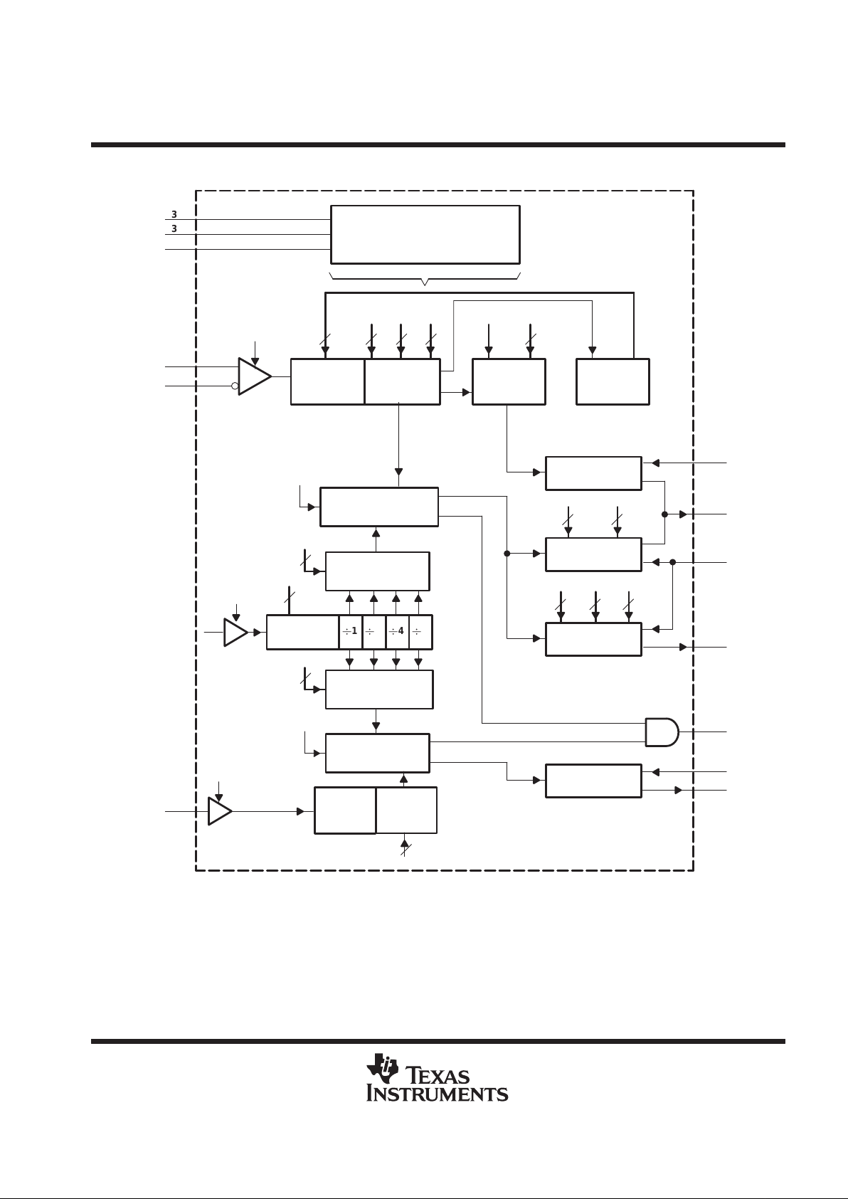
frequency synthesizer
The frequency synthesizer consists of the serial data interface, the main channel synthesizer, and the auxiliary
synthesizer. Figure 3 illustrates the functionality of the frequency synthesizer.
TRF3040
MODULATOR/SYNTHESIZER
SLWS057 – AUGUST 1999
19
POST OFFICE BOX 655303 • DALLAS, TEXAS 75265
PRINCIPLES OF OPERATION
Serial Input + Program Latches
Divide By
32/33
Prescaler
Main Divider
21282
PR MN1
NM2
NM3
Fractional
Accumulator
3
FMOD NF
Prescaler
Modulus
Control
Compensation
Charge Pump
Main Phase
Detector
Main Reference
Select
Reference
Divider
Auxiliary Reference
Select
EM
2
RSM
12
NR
Auxiliary Phase
Detector
2
RSA
EM + EA
EA
EA
13
NA
RF
DATA
CLOCK
STROBE
RXLO
INR
INA
RN
PHP
PHI
PHA
LOCK
EM
RA
Proportional
Charge Pump
8
CN
2
CL
Integral
Charge Pump
8
CN
2
CL
Auxiliary
Charge Pump
4
CK
Divide By
8/9
Prescaler
124
8
34
33
3
4
31
43
47
46
48
42
41
1
32
Auxiliary
Divider
Figure 3. Frequency Synthesizer Functional Block Diagram

TRF3040
MODULATOR/SYNTHESIZER
SLWS057 – AUGUST 1999
20
POST OFFICE BOX 655303 • DALLAS, TEXAS 75265
PRINCIPLES OF OPERATION
serial programming input
The TRF3040 operates using CLOCK, DATA, and STROBE pins of the serial data interface. The serial
programming data is structured into 24-bit words, of which one or four bits are dedicated address bits.
Figure 4 shows the format and the content of each word. Table 4 lists the symbols, number of bits, and the
function for each word used in the standard programming mode (AL T = 0). Similarly, the alternate programming
mode (ALT = 1) is described in Figure 5 and Table 5.
Figure 6 shows the timing diagram for the serial input. When the STROBE goes low, the signal on the DATA
input is clocked into a shift register on the positive edges of the CLOCK. When the STROBE goes high,
depending on the 1 or 4 address bit(s), data is latched into different working or temporary registers. To fully
program the modulator/synthesizer, five words must be sent: G, D, C, B, and A. The E-word is for testing
purposes only.
The A-word contains new data for the main divider. The A-word is loaded into the working registers only when
a main divider synchronization signal is active to avoid phase jumps when reprogramming the main divider.
The data for CN and PR is stored by the B-word in temporary registers. The data in these temporary registers
is loaded into the work registers together with the A-word. This avoids false main-divider input when the A-word
is loaded.
The value of the auxiliary divider ratio, NA, is defined by a 13-bit field, and the operational mode of the main
synthesizer is determined by the least significant bit (LSB) of the C-word:
Standard mode: ALT = 0
Alternate mode: ALT = 1
The content of the D-word defines the operation of the reference divider. The OR function of bits EA and EM
enables the buffer/amplifier input stage. The reference divider ratio is determined by the value of NR. The main
and auxiliary synthesizer sections can individually select a reference postscaler division of 1, 2, 4, or 8 by
selecting fields RSM and RSA, respectively.
The G-word programs all other functions: VGA power control, ÷ N (TXIF loop), SE (TXIF synthesizer loop
enable), AMPS and DAMPS modes, and sleep mode.
The E-word is for testing purposes only and is reset when programming the D-word.

TRF3040
MODULATOR/SYNTHESIZER
SLWS057 – AUGUST 1999
21
POST OFFICE BOX 655303 • DALLAS, TEXAS 75265
PRINCIPLES OF OPERATION
0 NF NM1
NM3 NM2
10000000 CN CK CL PR
1 0 1 0 NR RSM RSA
1111
A
B
D
E
1 0 1 1 PC N Spare
G
M
O
D
E
S
E
S
M
E
M
E
A
F
M
O
D
T
D0
WORD
D23
1001 NA 000000
C
A
L
T
S
p
a
r
e
S
p
a
r
e
S
p
a
r
e
S
p
a
r
e
NM2
Figure 4. Serial Input Word Format (Standard Programming, ALT = 0)

TRF3040
MODULATOR/SYNTHESIZER
SLWS057 – AUGUST 1999
22
POST OFFICE BOX 655303 • DALLAS, TEXAS 75265
PRINCIPLES OF OPERATION
Table 4. Standard Programming (ALT = 0) Function Table (see Notes 4 and 5)
SYMBOL BITS FUNCTION
NM1 12 Number of main divider cycles when the prescaler is programmed in ratio R1
†
NM2 8 if PR = X1
4 if PR = X0
Number of main divider cycles when the prescaler is programmed in ratio R2
†
NM3 4 if PR = X0
0 otherwise
Number of main divider cycles when the prescaler is programmed in ratio R3
†
PR 2 Main synthesizer prescaler type in use: PR = X1: modulus 2 prescaler (64/65)
PR = X0: modulus 3 prescaler (64/65/72)
NF 3 Main synthesizer fractional-N increment
FMOD 1 Main synthesizer fractional-N modulus selection flag:
1 = modulo 8
0 = modulo 5
CN 8 Current setting factor for main charge pumps
CL 2 Acceleration factor for proportional charge pump current
CK 4 Acceleration factor for integral charge pump current
EM 1 Main divider enable flag (see T able 11)
EA 1 Auxiliary divider enable flag (see Table 11)
RSM 2 Reference select for main phase detector
RSA 2 Reference select for auxiliary phase detector
NR 12 Reference divider ratio
NA 13 Auxiliary divider ratio
N 2 TXIF synthesizer divider ratio, ÷N, N = 6, 7, 8, 9 (see Note 6)
PC 7 Variable gain amplifier (VGA) power control function (see Table 14)
SE 1 TXIF synthesizer on/off. SE=1, TXIF synthesizer on; SE=0, TXIF synthesizer off
SM 1 Sleep mode bit; SM bit shuts down the synthesizers and the modulator section (see T able 3)
MODE 1 Mode control: MODE=1, digital (DAMPS); MODE=0, analog (AMPS) (see Note 7)
ALT 1 Alternate programming bit; AL T=0, standard (STD) mode; ALT=1, enhanced (ALT) mode (see Note 8)
T 19 T est mode connection of internal signals to lock pin: see
test modes
section
†
Not including reset cycles and fractional-N effects. R1 = 64, R2 = 65, R3 = 72.
NOTES: 4. Data bits are shifted in on the leading clock edge, with the least significant bit (LSB) first in and the most significant bit (MSB) last.
5. On the rising edge of the strobe and with the address decoder output = 1, the contents of the input shift register are transferred to
the working registers. The strobe rising edge comes one-half clock period after the clock edge on which the MSB of a word is shifted
in.
6. Field bits setting for the TXIF synthesizer divider ratio
FIELD BIT
N1 N0
B
N
0 0 6
0 1 7
1 0 8
1 1 9
7. The MODE bit allows a reduction in current for the DUALTX output driver while in AMPS mode.
8. The ALT programming bit allows the user to specify an enhanced programming scheme which allows for a fully programmable
fractional modulus of 1 to 16 for the main synthesizer.

TRF3040
MODULATOR/SYNTHESIZER
SLWS057 – AUGUST 1999
23
POST OFFICE BOX 655303 • DALLAS, TEXAS 75265
PRINCIPLES OF OPERATION
0NF NM
1000 G CN CK CL
1 0 0 1 NA FMOD 0
1 0 1 0 NR RSM RSA
1111
MSB LSB
WORD
A
0
B
C
D
E
1 0 1 1 PC N Spare
G
M
O
D
E
S
E
S
M
E
M
E
A
A
L
T
D23 D0
T
0
M
C
P
A
C
P
S
p
a
r
e
S
p
a
r
e
S
p
a
r
e
S
p
a
r
e
Figure 5. Serial Input Word Format (Alternate Programming, ALT = 1)

TRF3040
MODULATOR/SYNTHESIZER
SLWS057 – AUGUST 1999
24
POST OFFICE BOX 655303 • DALLAS, TEXAS 75265
PRINCIPLES OF OPERATION
Table 5. Alternate Programming (ALT = 1) Function Table
SYMBOL BITS FUNCTION
NF 4 Main synthesizer fractional-N increment
NM 18 Overall main divider integer division ratio
CN 8 Binary current-setting factor for main charge pumps
G 4 Speed-up mode duration (number of reference divider cycles)
CK 4 Binary acceleration factor for integral charge pump current
CL 2 Binary acceleration factor for proportional charge pump current
MCP 1 Main charge pump polarity
ACP 1 Auxiliary charge polarity
NA 13 Auxiliary charge ratio
FMOD 5 Fraction accumulator modulus
NR 12 Reference divider ratio
RSM 2 Reference select for main phase detector
EM 1 Main divider enable flag (see Table 11)
RSA 2 Reference select for auxiliary phase detector
EA 1 Auxiliary divider enable flag (see Table 11)
N 2 TXIF synthesizer divider ratio, ÷N, N = 6, 7, 8, 9
PC 7 Variable gain amplifier (VGA) power control function (see Table 14)
SE 1 TXIF synthesizer on/off. SE=1, TXIF synthesizer on; SE=0, TXIF synthesizer off
SM 1 Sleep mode bit: SM bit shuts down the synthesizers and the modulator section (see Table 3)
MODE 1 Mode control: mode=1, digital (DAMPS); mode=0, analog (AMPS)
ALT 1 Alternate programming bit: ALT=0, standard (STD) mode; ALT=1, enhanced (ALT) mode
T 19 Test mode connection of internal signals to LOCK pin (see
test modes
section)
D0 D1 D22 D23 D0
Valid Data Change
Last
Clock
First
Clock
Clock Disabled
Store Data
Clock Enabled – Shift In Data
Data
Clock
Strobe
t
su
t
h
t
su
t
su
Figure 6. Serial Input Timing Sequence

TRF3040
MODULATOR/SYNTHESIZER
SLWS057 – AUGUST 1999
25
POST OFFICE BOX 655303 • DALLAS, TEXAS 75265
PRINCIPLES OF OPERATION
reference variable divider
The internal reference signal INR, which is generated by the external crystal oscillator, is amplified to logic level
by a single-ended input buffer. The OR function of the serial input bits EM an EA enables this input buffer.
Subsequently , the output of the input buffer feeds the reference divider which consists of a 12-bit programmable
divide-by-NR (NR = 4 to 4095) and a four-section postscaler. The main and auxiliary synthesizer sections can
individually select a reference postscaler division of 1, 2, 4, or 8 by selecting RSM and RSA, respectively, as
shown in Figure 7.
Divide By NR
2
RSM = 00
RSM = 01
RSM = 10
RSM = 11
RSA = 11
RSA = 10
RSA = 01
RSA = 00
Main Phase
Detector
Auxiliary Phase
Detector
Main Select
Auxiliary Select
Reference Input
4
8
1
Figure 7. Reference Variable Divider
auxiliary variable divider
The input signal on INA is amplified to logic level by a single-ended input buffer , which has sufficient sensitivity
for direct connection to a typical VCO (200 mVpp at 200 MHz). The input stage is enabled when the serial control
bit EA = 1. The auxiliary divider consists of a 13-bit programmable divider with a 8/9 dual-modulus prescaler.
The 13-bit field divider is composed of two separate counters: a 3-bit NA2 counter and a 10-bit NA1 counter.
The total divider ratio value can be expressed as: NA = 8 (NA1 – NA2) + 9 NA2, where 7 v NA1 v 1023,
and 0 v NA2 v 7. This results in a continuous integral divide range of 56 to 8191. The detail of the 13-bit field
of the auxiliary divider is shown in Figure 8.
1001 NA 000000
C Word
A
L
T
NA1 NA2
Figure 8. 13-Bit Field Divider

TRF3040
MODULATOR/SYNTHESIZER
SLWS057 – AUGUST 1999
26
POST OFFICE BOX 655303 • DALLAS, TEXAS 75265
PRINCIPLES OF OPERATION
main variable divider – general
The input signal on RXLO is amplified to a logic level by a dif ferential-input comparator giving a common mode
rejection. The input stage is enabled by serial control bit EM = 1. Disabling means that all currents in the
comparator are switched off. The main variable divider is programmed using two different schemes: standard
and alternate.
The standard programming scheme (ALT=0) is referenced to a main divider section that implements a
dual/triple-modulus prescaler [(64/65)/(64/65/72)] design. The dual/triple modulus prescaler is actually
synthesized using a 32/33 dual-modulus prescaler with conversions that occur within the TRF3040 and are
transparent to the user.
Depending on the value of the prescaler select PR, the bit capacity for NM1, NM2, and NM3 is defined, as listed
in Table 6 (see also Figure 4).
Table 6. Main Variable Divider Bit Capacity
BIT CAPACITY
PR NM1 NM2 NM3
00 12 8 0
01 12 8 0
10 12 4 4
11 12 4 4
The total N-division ratio, as a function of the 64/65 dual-modulus and the 64/65/72 triple-modulus prescaler
can be expressed as:
D
N
total
= 64(NM1 + 2) + 65(NM2), where PR = 0X,
D
N
total
= 64(NM1 + 2) + 65(NM2) + 72(NM3 + 1), where PR = 1X.
For contiguous channels, the values of NM1, NM2, and NM3 are defined:
D
For PR = 0X: 61 v NMI v 4095 and 0 v NM2 v 63, which yields minimum and maximum divide ratios
of 4032 and 266303, respectively.
D
For PR = 1X: 14 v NMI v 4095 and 0 v NM2 v 15 and 0 v NM3 v 15, which yields minimum and
maximum divide ratios of 1096 and 264335, respectively.
The alternate programming scheme (AL T=1) is provided for ease of use. The 32/33 dual modulus prescaler is
the reference of the alternate programming scheme. Referring to the A-word of Figure 4 shown previously , the
main divider consists of 18-bit NM-field counters. The NM-field counter section is composed of two separate
counters: a 5-bit A-counter and a 13-bit B-counter, as shown in Figure 9. The prescaler divides by 33 until the
A-counter reaches terminal count and then divides by 32 until the B-counter reaches terminal count where upon
both counters reset and the cycle repeats.
The total NM division is defined as:
NM
Total
= 32(B – A) + 33(A), where 0 v A v 31 and 31 v B v 8191.
This results in a continuous integral divide range of 992 to 262143. If B < 31, the synthesizer no longer provides
contiguous channels. It is important to note that the value assigned to A is never greater than the value assigned
to B.

TRF3040
MODULATOR/SYNTHESIZER
SLWS057 – AUGUST 1999
27
POST OFFICE BOX 655303 • DALLAS, TEXAS 75265
PRINCIPLES OF OPERATION
main variable divider – general (continued)
32/33 Prescaler
13-Bit
B-Counter
5-Bit
A-Counter
18-Bit Register
13
5
18-Bit
Adder
18
5-Bit
Fraction Accumulator
18
4
5
5 Bits 13 Bits
N
A B
LSB MSB
Structure of N-Word
RFIN
N
NF
FMOD
to Phase Detector
Figure 9. Main Divider Organization
main variable divider – synchronization
The A-word is loaded into working registers only when a main divider synchronization signal is active in order
to avoid phase jumps when reprogramming the main divider. The synchronization signal is generated by the
main divider and is active when the main divider reaches its terminal count; also at this time, a main divider
output pulse is sent to the main phase detector. The new A-word is correctly loaded provided that the STROBE
signal is at an active high.
main variable divider – fractional accumulator
The TRF3040 main synthesizer loop can operate as a traditional integer-N feedback phase-locked loop or as
a fractional-N feedback phase-locked loop. The integer-N feedback loop divides the VCO frequency by integer
values of N that result in phase detector reference comparisons at the desired channel spacing. A fractional-N
feedback loop divides the VCO frequency by an integer term plus a fractional term that results in phase detector
reference comparisons at integer multiples of the desired system channel spacing.
Integer-N division: VCO frequency N = Phase detector reference frequency
= channel spacing
Fractional-N division: VCO frequency (N + NF/FMOD)= Phase detector reference frequency
= FMOD × channel spacing
where 0 ≤ NF < FMOD and 1 ≤ FMOD ≤ 16.
Because the programmable main counter and prescaler can not divide by a fraction of an integer, fractional-N
division is accomplished by averaging main divider cycles of division by N and N+1. A fractional accumulator
that is programmed with values of NF and FMOD is responsible for causing the main counter and prescaler
sections to divide by N or N+1.
The fractional accumulator operates modulo-FMOD and is incremented by NF at the completion of each main
divider cycle. When the fractional accumulator overflows, division by N+1 occurs. Otherwise, the main counters
and prescaler divide by N; division by N+1 is transparent to the user. Table 7 shows the contents of the fractional
accumulator and the resulting N or N+1 division for two fractional division ratios.

TRF3040
MODULATOR/SYNTHESIZER
SLWS057 – AUGUST 1999
28
POST OFFICE BOX 655303 • DALLAS, TEXAS 75265
PRINCIPLES OF OPERATION
Table 7. Fractional Accumulator Operation
NF = 3, FMOD = 8 NF = 6, FMOD = 8
ACCUMULATOR
NUMERATOR
STATE
ACCUMULATOR
NUMERATOR
STATE
3 ÷ N 6
÷ N
6
÷ N
4
÷ N + 1, overflow
1 ÷ N + 1, overflow 2
÷ N + 1, overflow
4
÷ N
0
÷ N + 1, overflow
7
÷ N
6
÷ N
2
÷ N + 1, overflow
4
÷ N + 1, overflow
5
÷ N
2
÷ N + 1, overflow
0
÷ N + 1, overflow
0
÷ N + 1, overflow
For example, suppose that the main synthesizer input frequency is 1958.97 MHz, the main phase detector
reference frequency is 240 kHz, and a channel spacing of 30 kHz is realized. The value of
FMOD = 8 would be selected because 240 kHz/30 kHz = 8. Dividing the main synthesizer input frequency by
the reference frequency results in 1958.97 ÷ 0.24 = 8162.375 = 8162 + 3/8. As a result, the fractional
accumulator overflow cycle of this particular frequency is described with NF=3 and FMOD=8 (see Table 7).
Figure 10 illustrates the division by N and N+1 for this 3/8 fractional channel example.
N
(8162)
N
(8162)
N + 1
(8163)
N
(8162)
N
(8162)
N + 1
(8163)
N
(8162)
N + 1
(8163)
Number of Main
Divider Pulses
RF Input
Main Divider Out
Figure 10. 3/8 Fractional Channel Main Divider Operation
The mean division over the complete fractional accumulator cycle as shown in Figure 9 is:
N
MEAN
+
8162)8162)8163)8162)8162)8163)8162)8163
8
+
8162.375
+
8162)3ń8.
Therefore, fractional channels are available every 30 kHz or 240 kHz
1
FMOD
+
240 kHz
8
.
main divider – integer channels
In the case where NF = 0, only division by N occurs and the fractional accumulator essentially is steady state
with a numerator of 0 and never increments or overflows. A channel that requires NF = 0 is a pure integer
channel because the fractional term of
NF
FMOD
is zero.

TRF3040
MODULATOR/SYNTHESIZER
SLWS057 – AUGUST 1999
29
POST OFFICE BOX 655303 • DALLAS, TEXAS 75265
PRINCIPLES OF OPERATION
main divider – fractional-N sidebands and compensation
Programming a fractional-N channel means the main divider and prescaler divide by N or N + 1 as dictated by
the operation of the fractional accumulator. Because the main divider operation is integer in nature and the
desired VCO frequency is not, the output of the main phase detector is modulated with a resultant fractional-N
phase ripple that, if left uncompensated, produces sideband energy. This phase ripple is proportional and
synchronized to the contents of the fractional accumulator that is used to control fractional-N sideband
compensation. Only channels that require a nonzero value of NF have the fractional-N sideband energy . The
fractional-N sidebands appear at offset frequencies from the VCO fundamental tone, which are multiples of
NF/FMOD. Figure 11 shows the fractional-N phase detector ripple for a 3/8 fractional channel.
240 kHz
036147250
Main Phase
Detector Reference
Main Phase
Detector VCO
Feedback
Main Phase
Detector Fractional-N
Ripple
Fractional
Accumulator State
Figure 11. Fractional-N Phase Detector Ripple for 3/8 Fractional Channel
The TRF3040 has internal circuitry that provides a means to compensate for the phase detector fractional-N
phase ripple thereby significantly reducing the magnitude of the fractional-N sidebands. Because the current
waveform output of the main phase-locked loop (PLL) proportional charge pumps is modulated with the phase
detector fractional-N phase ripple, a fractional-N compensation charge pump output is summed with the main
PLL proportional charge pump.
Figure 12 shows the fractional-N ripple magnitude on the main PHP charge pump output. The magnitude is
essentially constant and the pulse width is modulated with the contents of the fractional accumulator. The area
under the Main PHP charge pump curve represents the amount of charge delivered to the system loop filter
network. In order to minimize fractional-N sidebands in the VCO spectrum, the compensation current waveform
is generated to have
equal
and
opposite
sign magnitude
areas
as the main PHP charge pump.
036147250
Pulse Width
Modulation
Pulse Amplitude
Modulation
Fractional
Accumulator State
Main PHP Charge Pump
Fractional-N Ripple
Magnitude
Compensation Charge
Pump Fractional-N
Ripple Magnitude
mA
µA
Figure 12. Main PHP and Compensation Charge Pump Fractional-N Waveforms for 3/8 Fractional Channel

TRF3040
MODULATOR/SYNTHESIZER
SLWS057 – AUGUST 1999
30
POST OFFICE BOX 655303 • DALLAS, TEXAS 75265
PRINCIPLES OF OPERATION
main divider – fractional-N sidebands and compensation (continued)
The compensation waveform is pulse-amplitude modulated with the contents of the fractional accumulator. The
main PHP pulse magnitude is much larger than the compensation pulse magnitude, but the compensation pulse
has a much longer duration than that of the main PHP pulse. The compensation pulse is optimally centered
about the main PHP charge pump pulse in order to avoid additional sideband energy due to phase-offset
between the main and compensation pulses.
The following step illustrates a method for determining correct values for RN, RF, and CN for minimal
fractional-N sidebands based on VCO frequency and reference frequency.
Assumptions:
The main VCO is locked on channel.
The 1970 ± 15-MHz main VCO operation, 1958.19 – 1983.15 MHz.
19.44-MHz reference frequency
240-kHz phase detector reference frequency
288-µA peak main PHP current
1. Determine the fundamental fractional-N pulse-width portion of the main PHP charge-pump output
waveform for the lower, upper, and mean frequencies.
Frac
PW–LWR
+
1
f
PD
–
N
f
VCO
+
1
240 kHz
–
8159
1958.19 MHz
+
63.83 ps,
Frac
PW–UPR
+
1
f
PD
–
N
f
VCO
+
1
240 kHz
–
8263
1983.15 MHz
+
63.031 ps,
Frac
PW–MEAN
+
Frac
PW*LWR
)
Frac
PW–UPR
2
+
63.83 ps)63.031 ps
2
+
63.43 ps.
Therefore, the mean unit pulse-width of the fractional-N portion of the main PHP charge-pump output
waveform over the VCO frequencies of interest is 63.43 ps. This fundamental pulse width is modulated by
the contents of the fractional accumulator. For the 3/8 fractional-N channel example, the pulse width varies
as shown in Table 8.
Table 8 also shows the area of the fractional-N portion of the main PHP charge-pump waveform.
Table 8. Main PHP Fractional-N Pulse Widths and Areas for 3/8 Channel
NF = 3, FMOD = 8
ACCUMULATOR
STATE
MAIN PHP FRACTIONAL PULSE WIDTH
(E–12 SECONDS)
MAIN PHP FRACTIONAL AREA
(E–12 SECOND X AMPS)
3 3 ×
PW–Mean
= 190.29 190.29 ps × 288 µA = 0.54804
6 6 ×
PW–Mean
= 380.58 380.58 ps × 288 µA = 0.109607
1 1 ×
PW–Mean
= 63.43 63.43 ps × 288 µA = 0.018268
4 4 ×
PW–Mean
= 253.72 253.72 ps × 288 µA = 0.073071
7 7 ×
PW–Mean
= 444.01 444.01 ps × 288 µA = 0.127875
2 2 ×
PW–Mean
= 126.86 126.86 ps × 288 µA = 0.036536
5 5 ×
PW–Mean
= 317.15 317.15 ps × 288 µA = 0.091339
0 0 ×
PW–Mean
= 0 0 ps × 288 µA = 0

TRF3040
MODULATOR/SYNTHESIZER
SLWS057 – AUGUST 1999
31
POST OFFICE BOX 655303 • DALLAS, TEXAS 75265
PRINCIPLES OF OPERATION
main divider – fractional-N sidebands and compensation (continued)
1. Determine the pulse width of the compensation charge-pump output waveform.
Comp
PW
+
1
f
Ref
+
1
19.44 MHz
+
51.440 ns
2. Determine the fundamental compensation charge pump current magnitude using the fundamental main
PHP fractional area.
Comp
Mag
+
Frac
Area
Comp
PW
+
0.018268 psA
51.440 ns
+
0.3551mA
Table 9 shows the magnitude of the compensation pulse as a function of the fractional accumulator.
Table 9. Compensation Pulse Magnitudes for 3/8 Channel
NF = 3, FMOD = 8
Accumulator
Numerator
Compensation Pulse
Magnitude (µA)
3 3 × 0.3551 = 1.0653
6 6 × 0.3551 = 2.136
1 1 × 0.3551 = 0.3551
4 4 × 0.3551 = 1.4204
7 7 × 0.3551 = 2.4857
2 2 × 0.3551 = 0.7102
5 5 × 0.3551 = 2.4857
0 0 × 0.3551 = 0
3. Using the result of Step 2, determine the value of RF to give the fundamental compensation pulse
magnitude.
RF(k
W)+
VBG
40 x Comp
Mag
(
m
A
)
+
1.25
40 x 0.3551
+
88 kW.
4. Determine values of CN and RN to give a main PHP charge-pump peak current of 500 µA. Assume a
mid-range value of CN equal 128.
RN(k
W)+ǒ18.75
CN
256
1
I(mA
)
Ǔ
–0.75
+ǒ18.75
128
256
1
0.288 mA
Ǔ
–0.75+32.55 kW.
5. The value of the fundamental compensation pulse magnitude calculated in step 3 is fixed, and the
compensation pulse width calculated in step 2 is also fixed. However, because the VCO can tune over a
significant range of frequencies, the pulse width of the fractional-N portion of the main PHP charge-pump
waveform varies, thus the area of the same waveform varies. In order to maintain equal areas under the
fractional-N portion of the main PHP charge-pump and compensation waveforms, CN is varied with the
VCO frequency . As the VCO frequency increases, the fractional-N portion of the main PHP charge-pump
waveform pulse width decreases proportionally, thereby decreasing the area under the same waveform.
Therefore, CN must be adjusted to equalize the main PHP and compensation waveform areas. The lower
and upper fractional–N pulse widths are calculated using the equations in step 1, as follows:
Frac
PW-LWR
= 64.168 ps for f
VCO
= 1958.19 MHz
Frac
PW-UPR
= 63.064 ps for f
VCO
= 1983.15 MHz

TRF3040
MODULATOR/SYNTHESIZER
SLWS057 – AUGUST 1999
32
POST OFFICE BOX 655303 • DALLAS, TEXAS 75265
PRINCIPLES OF OPERATION1234
main divider – fractional-N sidebands and compensation (continued)
The fundamental area mean value of the fractional-N portion of the main PHP charge-pump waveform was
calculated to be 0.018268 pSA. If the fundamental area of the fractional-N portion of the main PHP
charge-pump waveform uses the actual pulse widths calculated in step 1 in place of the average pulse
width, the fractional-N main PHP areas are as follows:
Frac
Area-L WR
= 63.83 ps x 0.288 mA = 0.018383 (E-12 second × Amps),
Frac
Area-UPR
= 63.031 ps x 0.288 mA = 0.018383 (E-12 second × Amps).
The actual areas under the fractional-N portion of the main PHP waveform require slight modification in the
charge-pump current. The variation of CN required for area equalization can be determined using a simple
ratio form:
CN
LWR
+
Frac
Area–AVG
Frac
Area–LWR
CN
AVG
+
0.018268
0.018383
128+127,
CN
UPR
+
Frac
Area–AVG
Frac
Area–UPR
CN
AVG
+
0.018268
0.018153
128+129.
Therefore, CN values would vary from 127–129 over the VCO frequency range of 1958.19–1983.15 MHz
for optimum fractional-N sideband suppression. Due to component and circuit tolerances, additional
deviations in CN may be appropriate.
phase detectors
The main and auxiliary synthesizer sections (see Figure 13) incorporate dual D-type flip-flop phase-frequency
detectors (PFD). The PFD has gain with phase error over a range of +/–2π and exhibits infinite pull-in range.
Dead-band compensation about zero phase error is provided by forcing the sourcing and sinking charge pumps
to have a minimum on-time rate of 1/f
Ref
when the loop is operating in a locked condition.
The phase detectors can be programmed for polarity sense. Normally , external system VCOs have a positive
slope control voltage-frequency characteristic. Some VCOs have a negative slope characteristic. The TRF3040
main and auxiliary phase detectors can be programmed for use with positive or negative slope VCOs using the
MCP
and
ACP
fields, respectively, in the B word (EPM mode).
For positive slope VCOs: MCP = ACP = 0; for negative slope VCOs: MCP = ACP = 1.

TRF3040
MODULATOR/SYNTHESIZER
SLWS057 – AUGUST 1999
33
POST OFFICE BOX 655303 • DALLAS, TEXAS 75265
PRINCIPLES OF OPERATION
phase detectors (continued)
D
SET
Q
Q
CLR
D
SET
Q
Q
CLR
1
1
Reference Divider
/NR
Main or Auxiliary
Reference Divider
/N or /NR
VDDA
VSSA
Charge Pump
Output
REFIN
REFIN or AUXIN
Figure 13. Main and Auxiliary Phase Detector Circuit
charge-pump current plans
The TRF3040 uses internal band-gap references and external resistors to develop biasing reference currents
for the various charge pump sections. Three terminals are designated for the external resistors: RN, RF, and
RA. Internal, programmable coefficients CN, CL, and CK are also used. Table 10 shows how the external
resistors are used to achieve desired charge-pump peak currents.
Table 10. Charge Pump Current Plans
PARAMETER MODE CONDITION UNIT
Main PHP
NORMAL
+
VBG
CN
17(RN)300)
Normal RN in kΩ mA
Main PHP
SPEED UP
+
2
CL)1
CN
V
BG
17(RN)300)
Speed-up RN in kΩ mA
Main PHI
PSPEED UP
+
2
CL)1
VBG CN
CK
17 (RN)300)
Speed-up RN in kΩ mA
†
Fractional
PHP
NORMAL
+
V
BG
40 RF
Normal RF in kΩ µA
Fractional
PHP
SPEED UP
+
TBD
Speed-up
Fractional
PHI
SPEED UP
+
TBD
Speed-up
Peak auxiliary current PHAPK+
ǒ
1.25
RA
x20
Ǔ
Normal RA in kΩ mA
†
The compensation charge-pump current is a pulse-amplitude modulated with the contents of the fractional accumulator. See the section on Main
Divider – Fractional-N Sidebands and Compensation.

TRF3040
MODULATOR/SYNTHESIZER
SLWS057 – AUGUST 1999
34
POST OFFICE BOX 655303 • DALLAS, TEXAS 75265
PRINCIPLES OF OPERATION
charge-pump current plans (continued)
The average charge-pump current for the PHP, PHI, and PHA terminals is defined by:
I
AVG
+
q
error
2
p
xIPK.
loop enable/disable
The main and auxiliary loops can be enabled and disabled by the contents of enable bits EM and EA,
respectively , as described in Table 11. When disabled, all currents in the RF input stages are switched off; the
bias currents for the respective charge-pump circuits are switched off as well. When both loops are disabled
(EM = EA = 0), the reference input stage currents are switched off. The reference chain can be turned off
because the serial interface operates independent of the reference input for the loading of serial words.
Table 11. Loop Enable/Disable
EM EA ENABLED DISABLED
0 0 Main, auxiliary, reference
0 1 Auxiliary , reference Main
1 0 Main, reference Auxiliary
1 1 Main, auxiliary, reference
speed-up mode
When the main synthesizer frequency is changed, it may be desirable to increase the loop bandwidth for a short
time in order to achieve a faster lock time. The proportional charge-pump current is increased and the integral
charge-pump current is switched on for the duration of speed-up mode. The
charge-pump current plans
section,
illustrates how the charge-pump currents are a function of the external resistor RN and the programmable
coefficients CN, CL, and CK.
The duration of speed-up mode is controlled by two different means that are dependent on the operational
programming scheme of the TRF3040 device: either the alternate (ALT) or standard (STD) programming
scheme. In the alternate programming scheme, the speed-up mode duration is controlled as a function of the
G-field in the B-word and the reference frequency divider period.
Duration
ALT
+G
NR
f
REFIN
, ALT speed-up mode duration
The content of the G-field is the value of the most significant 4 bits of a total 8-bit programming operation. The
least significant 4 bits are static 1 bits. Therefore the minimum of Duration
ALT
is:
Duration
ALT
min
+15
NR
f
REFIN
,
and the maximum of Duration
ALT
is:
Duration
ALTmax
+
255
NR
f
REFIN
,
When the TRF3040 is operated in standard programming scheme, the speed-up mode duration is a function
of the STROBE signal associated with the A-word. When the STROBE signal following an A-word write
operation goes active, speed-up mode currents begin and persist until the STROBE signal is returned to an
inactive state.

TRF3040
MODULATOR/SYNTHESIZER
SLWS057 – AUGUST 1999
35
POST OFFICE BOX 655303 • DALLAS, TEXAS 75265
PRINCIPLES OF OPERATION
lock detect
The LOCK terminal can be polled to determine the synthesizer lock condition of either or all three loops. The
lock detect function is described by the Boolean expression:
LOCK
+ǒLD
Main
)
EMǓ ǒLD
Aux
)
EAǓ ǒTXIF_LD)SE
Ǔ
test modes
The LOCK terminal may be used for test operation. When test modes are enabled, the LOCK terminal is
connected to internal nodes of the TRF3040. T est modes are enabled by writing to the E-word. Test modes are
disabled by writing zeros to the E-word. These bits are also reset to zero when the D-word is written. Table 12
lists all available test modes and associated programming bits.
Table 12. Test Modes
TEST MODE T19 – T16 T15 – T12 T11 – T8 T7 – T4 T3 – T0
Lock detect 0000 0000 0000 0000 0000
Fractional overflow 0000 0000 0000 0000 0100
Auxiliary_VCO divider 0000 0000 0000 0000 0101
Main_VCO divider 0000 0000 0000 0000 0110
Main reference divider 0000 0000 0000 0000 0111
Force lock pin HIGH 1100 0000 0000 0000 0000
Force lock pin LOW 0100 0000 0000 0000 0000
Auxiliary and main pumps UP 0000 0000 0000 1010 1000
Auxiliary and main pumps DOWN 0000 0000 0000 0101 1000
Fractional pump test 0000 0000 0010 0000 0000
Main prescaler bypass 0000 0000 0001 0000 01 10
Auxiliary prescaler bypass 0000 1000 0000 0000 0101
Enable reference chain test 0001 0000 0000 0000 0111
transmit modulator
The transmit modulator section of the TRF3040 is composed of a transmit intermediate frequency synthesizer
reset circuit that controls the operation of the transmit modulator, a transmit intermediate frequency
phase-locked loop that generates the intermediate transmit frequency (TXIF), a single-sideband suppressed
carrier (SSBSC) converter, an I/Q modulator, and an output VGA.
transmit intermediate frequency synthesizer reset circuit
Figure 14 and Figure 15 reveal that the falling edge of the STROBE toggles the Q output of flip flop (1) to a 1
state, which enables the TXIF phase detector, the TXIF_VCO, the divide-by-N, the TXIF buffer, and the SSB
converter. Once the synthesizer is locked, the TXEN signal (enable = 1) turns on the modulator and the VGA.
The rising edge of TXEN has no affect on SYNEN as shown in Figure 15. However, the falling edge of TXEN
toggles the Q output of flip flop (2) to a 0 state which resets flip flop (1) and causes SYNEN to go to a 0 state,
thus disabling the transmit intermediate synthesizer, the I/Q modulator, and the VGA.

TRF3040
MODULATOR/SYNTHESIZER
SLWS057 – AUGUST 1999
36
POST OFFICE BOX 655303 • DALLAS, TEXAS 75265
PRINCIPLES OF OPERATION
D
CLK
Q
Q
D
CLK
Q
Q
(3)
(1)
R
R
D
Q
CLK
Q
Temporary Register
SE
Working Register
V
CC
TXEN
(2)
SYN
EN
Clock
Data
Strobe
MSB (G Word)
1011
Figure 14. Transmit Intermediate Frequency Synthesizer Reset Circuit
LSB MSB
Locked
Time
Transmit
Pulse
Width
TXEN
Data
Clock
Strobe
SYN
EN
Figure 15. Transmit Intermediate Frequency Synthesizer Reset Circuit Timing Diagram

TRF3040
MODULATOR/SYNTHESIZER
SLWS057 – AUGUST 1999
37
POST OFFICE BOX 655303 • DALLAS, TEXAS 75265
PRINCIPLES OF OPERATION
transmit intermediate frequency (TXIF) synthesizer
The transmit intermediate frequency (TXIF) PLL portion of the TRF3040 design consists of the following
functional blocks: a reference oscillator, a TXIF phase detector, a divide-by-N (÷N), a TXIF_VCO, and an
external passive loop filter.
reference oscillator
The reference crystal oscillator (XT AL OSC) generates the internal reference signal INR. This signal is directly
fed to the phase detector of the PLL in the transmit modulator section and to three other different buffers. The
first buffer feeds the reference divider of the main phase detector and the auxiliary phase detector . The second
buffer , MCLK, is used to provide a clock for external digital circuitry , which is always on. The third buffer , RCLK,
is used as a clock for the external circuitry that is used in standby and transmit modes.
TXIF phase detector and charge pump
The phase comparator compares the output of the divider with the reference oscillator. It provides an output
proportional to the phase difference between the divided down TXIF_VCO and the reference. This output is then
filtered and used as the control voltage input to the TXIF_VCO. The phase detector is a Gilbert multiplier cell
type, with a linear output from 0 to π ( π/2 ± π/2), followed by a charge pump. The charge-pump peak output
current could be programmable to 6.4 mA using an external resistor.
TXIF lock detect
A lock detect signal is provided and ANDed together with lock detect signals from both the main channel
synthesizer and auxiliary synthesizer. While in standby mode, the lock detect signal is forced to a valid lock state
so that the lock detect signal will indicate when the main and auxiliary phase detectors achieve phase lock.
divide-by-N
The ÷N is a 2-bit programmable divider that can be configured for any integer division from 6 to 9. The field bits
setting for this ÷N is described in Note 6. The divider converts the VCO output down to the reference frequency
before feeding it into the phase comparator.
TXIF_VCO
The voltage controlled oscillator, TXIF_VCO, generates the transmit IF frequency, TXIF, between 90 MHz and
200 MHz. This TXIF_VCO is configured using an external parallel inductor and a dual common-cathode
tuning-varactor diode. DC blocking capacitors are used to isolate the varactor control voltage from the VCO tank
dc bias voltages.
SSBSC converter and TXIF buffer
The TXIF buffer provides isolation between the SSBSC converter and the TXIF_VCO output. The converter is
an active Gilbert cell multiplier (matched pair) combined with two quadrature phase shift networks and a
band-pass filter. The SSBSC converter rejects the unwanted upper sideband that would normally occur during
the conversion process.

TRF3040
MODULATOR/SYNTHESIZER
SLWS057 – AUGUST 1999
38
POST OFFICE BOX 655303 • DALLAS, TEXAS 75265
PRINCIPLES OF OPERATION
I/Q modulator
The quadrature modulator is an active Gilbert cell multiplier (matched pair) with cross-coupled outputs. These
outputs are provided to the variable gain amplifier, DUALTX VGA.
variable gain amplifier (VGA) and power amplifier (PA) driver
The DUAL TX VGA power control circuit has a control range of 50 dB (–41 dBm to 9 dBm) with a monotonically
decreasing slope, 0.5 dB per step (typical), as shown in Figure 16. A 4:1 balun is used on the applications circuit
to transform the 200-W differential output impedance of the PA driver to a 50-W single-ended impedance for
testing purposes.
DUALTX Output Power – dBm
–20
–30
–40
–50
–10
0
VGA Power Control (PC) Code
10
0
4
12
20
28
36
44
52
60
68
76
84
92
100
108
116
8
16
24
32
40
48
56
64
72
80
88
96
104
112
Figure 16. Power Control

TRF3040
MODULATOR/SYNTHESIZER
SLWS057 – AUGUST 1999
39
POST OFFICE BOX 655303 • DALLAS, TEXAS 75265
MECHANICAL DATA
PT (S-PQFP-G48) PLASTIC QUAD FLATPACK
4040052/C 11/96
0,13 NOM
0,17
0,27
25
24
SQ
12
13
36
37
6,80
7,20
1
48
5,50 TYP
0,25
0,45
0,75
0,05 MIN
SQ
9,20
8,80
1,35
1,45
1,60 MAX
Gage Plane
Seating Plane
0,10
0°–7°
0,50
M
0,08
NOTES: A. All linear dimensions are in millimeters.
B. This drawing is subject to change without notice.
C. Falls within JEDEC MS-026
D. This may also be a thermally enhanced plastic package with leads connected to the die pads.

IMPORTANT NOTICE
T exas Instruments and its subsidiaries (TI) reserve the right to make changes to their products or to discontinue
any product or service without notice, and advise customers to obtain the latest version of relevant information
to verify, before placing orders, that information being relied on is current and complete. All products are sold
subject to the terms and conditions of sale supplied at the time of order acknowledgement, including those
pertaining to warranty, patent infringement, and limitation of liability.
TI warrants performance of its semiconductor products to the specifications applicable at the time of sale in
accordance with TI’s standard warranty. Testing and other quality control techniques are utilized to the extent
TI deems necessary to support this warranty. Specific testing of all parameters of each device is not necessarily
performed, except those mandated by government requirements.
CERT AIN APPLICATIONS USING SEMICONDUCTOR PRODUCTS MAY INVOLVE POTENTIAL RISKS OF
DEATH, PERSONAL INJURY, OR SEVERE PROPERTY OR ENVIRONMENTAL DAMAGE (“CRITICAL
APPLICATIONS”). TI SEMICONDUCTOR PRODUCTS ARE NOT DESIGNED, AUTHORIZED, OR
WARRANTED TO BE SUITABLE FOR USE IN LIFE-SUPPORT DEVICES OR SYSTEMS OR OTHER
CRITICAL APPLICATIONS. INCLUSION OF TI PRODUCTS IN SUCH APPLICA TIONS IS UNDERSTOOD T O
BE FULLY AT THE CUSTOMER’S RISK.
In order to minimize risks associated with the customer’s applications, adequate design and operating
safeguards must be provided by the customer to minimize inherent or procedural hazards.
TI assumes no liability for applications assistance or customer product design. TI does not warrant or represent
that any license, either express or implied, is granted under any patent right, copyright, mask work right, or other
intellectual property right of TI covering or relating to any combination, machine, or process in which such
semiconductor products or services might be or are used. TI’s publication of information regarding any third
party’s products or services does not constitute TI’s approval, warranty or endorsement thereof.
Copyright 1999, Texas Instruments Incorporated
 Loading...