

LOW-VOLTAGE 1.2-GHz FRACTIONAL-N/INTEGER-N SYNTHESIZER
SLWS030D– JUNE 1996 – REVISED OCTOBER 1998
D
1.2-GHz Operation
D
Two Operating Modes:
– Philips SA7025 Emulation Mode
Pin-for-Pin and Programming
Compatible
– Extended Performance Mode (EPM)
D
Dual RF – IF Phase-Locked Loops
D
Fractional-N or Integer-N Operation
D
Programmable EPM Fractional
Modulus of 1–16
D
Normal, Speed-Up, and Fractional
CLOCK
DATA
STROBE
V
SS
RFIN
RFIN
V
CCP
REFIN
RA
AUXIN
Compensation Charge Pumps
D
2.9-V to 5.1-V Operation
D
Low-Power Consumption
description
The TRF2050 is a low-voltage, low-power consumption 1.2-GHz fractional-N/integer-N frequency synthesizer
component for wireless applications. Fractional-N division and an integral speed-up charge pump are used to
achieve rapid channel switching. Two operating modes are available: 1) SA7025 emulation mode in which the
part emulates the Philips SA7025 fractional-N synthesizer and 2) extended performance mode (EPM), which
provides additional features including fractional accumulator modulos from 1 to 16 (compared to only 5 or 8 for
the SA7025) and programmable control of the speed-up mode duration (compared to the SA7025 method of
holding the strobe line high).
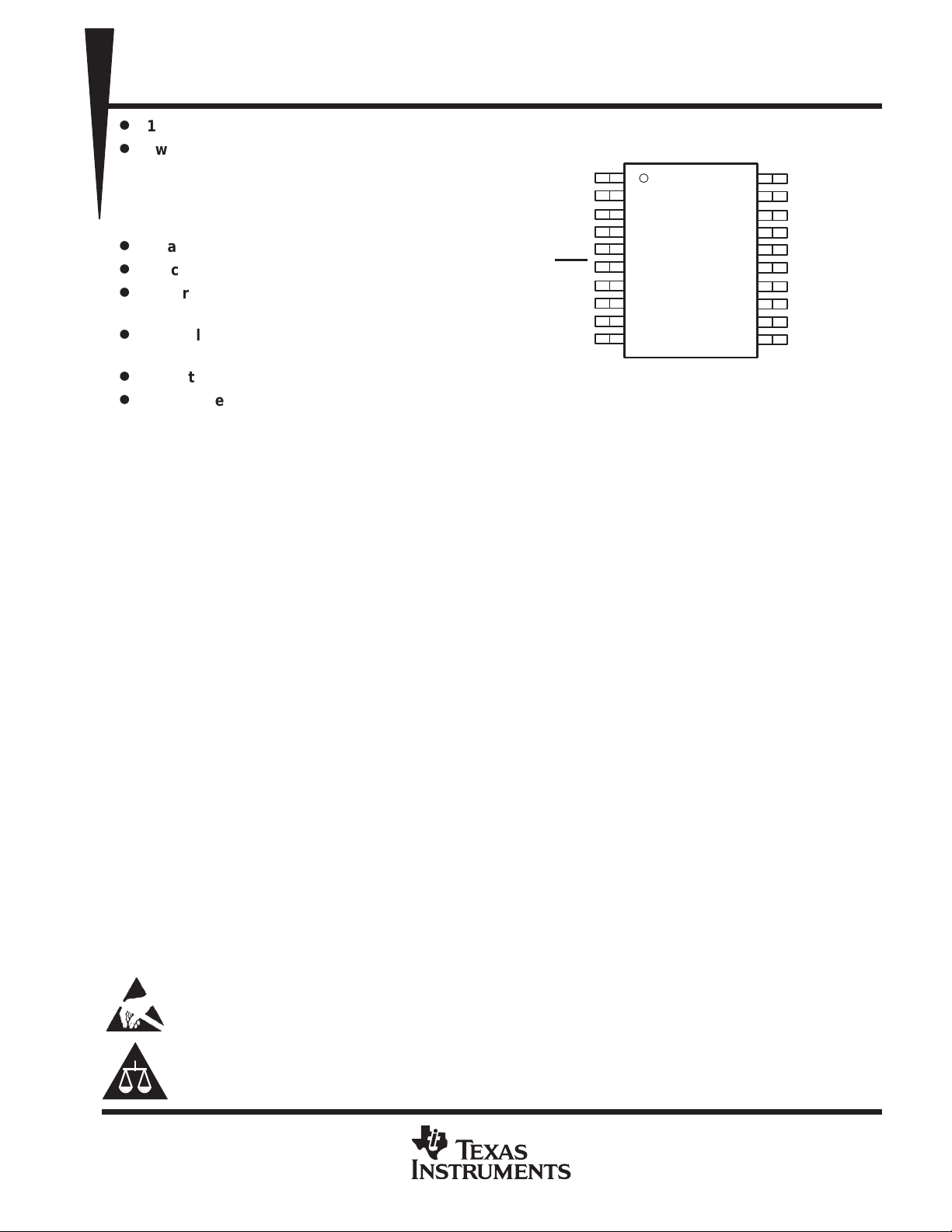
PW PACKAGE
(TOP VIEW)
1
2
3
4
5
6
7
8
9
10
20
19
18
17
16
15
14
13
12
11
TRF2050
V
DD
TSETUP
LOCK/TEST
RF
RN
V
DDA
PHP
PHI
V
SSA
PHA
Along with external loop filters, the TRF2050 provides all functions necessary for voltage-controlled oscillator
(VCO) control in a dual phase-locked loop (PLL) frequency synthesizer system. A main channel is provided for
radio frequency (RF) channels and an auxiliary channel for intermediate frequency (IF) channels. The
current-output charge pumps directly drive passive resistance-capacitance (RC) filter networks to generate
VCO control voltages. Rapid main-channel frequency switching is achieved with a charge pump arrangement
that increases the current drive and alters the loop-filter frequency response during the speed-up mode portion
of the switching interval.
These devices have limited built-in ESD protection. The leads should be shorted together or the device placed in conductive foam
during storage or handling to prevent electrostatic damage to the MOS gates.
Please be aware that an important notice concerning availability, standard warranty, and use in critical applications of
Texas Instruments semiconductor products and disclaimers thereto appears at the end of this data sheet.
PRODUCTION DATA information is current as of publication date.
Products conform to specifications per the terms of Texas Instruments
standard warranty. Production processing does not necessarily include
testing of all parameters.
POST OFFICE BOX 655303 • DALLAS, TEXAS 75265
Copyright 1998, Texas Instruments Incorporated
1
TRF2050
/
LOW-VOLTAGE 1.2-GHz FRACTIONAL-N/INTEGER-N SYNTHESIZER
SLWS030D– JUNE 1996 – REVISED OCTOBER 1998
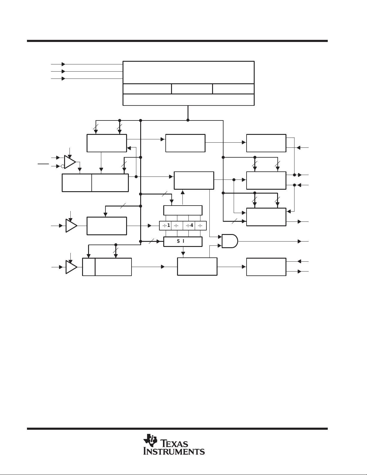
functional block diagram
2
DATA
RFIN
RFIN
1
3
5
6
8
10
EM
32/33
Prescaler
EM+EA
EA
FMOD
Accumulator
†
PA
4/1
5
Fraction
Main Divider
Reference
Divider
CLOCK
STROBE
REFIN
AUXIN
†
NF
(N/N+1)
NR
NA
Auxiliary
Divider
Serial Control Shift Registers
Common Registers EPM Registers 7025 Registers
‡
8
12
Conversion and Selection
4
N
18
12
SA
2
Control Lines
Fraction
Compensation
Phase
Detector
SM
2
Select
124
Select
Phase
Detector
CK
CN
CN
4
Compensation
Charge Pump
CL
8
Proportional
Charge Pump
CL
8
Integral
Charge Pump
Auxiliary
Charge Pump
17
RF
2
14
PHP
16
RN
2
13
PHI
18
LOCK
TEST
9
RA
11
PHA
†
Terminals 4, 7, 12, 15, and 20 are for supply voltage. Terminal 19 is for testing. These terminals are not shown.
‡
Conversion and selection block provides emulation of SA7025 64/65/72 triple-modulus prescaler operation using the TRF2050 32/33
dual-modulus prescaler .
2
POST OFFICE BOX 655303 • DALLAS, TEXAS 75265
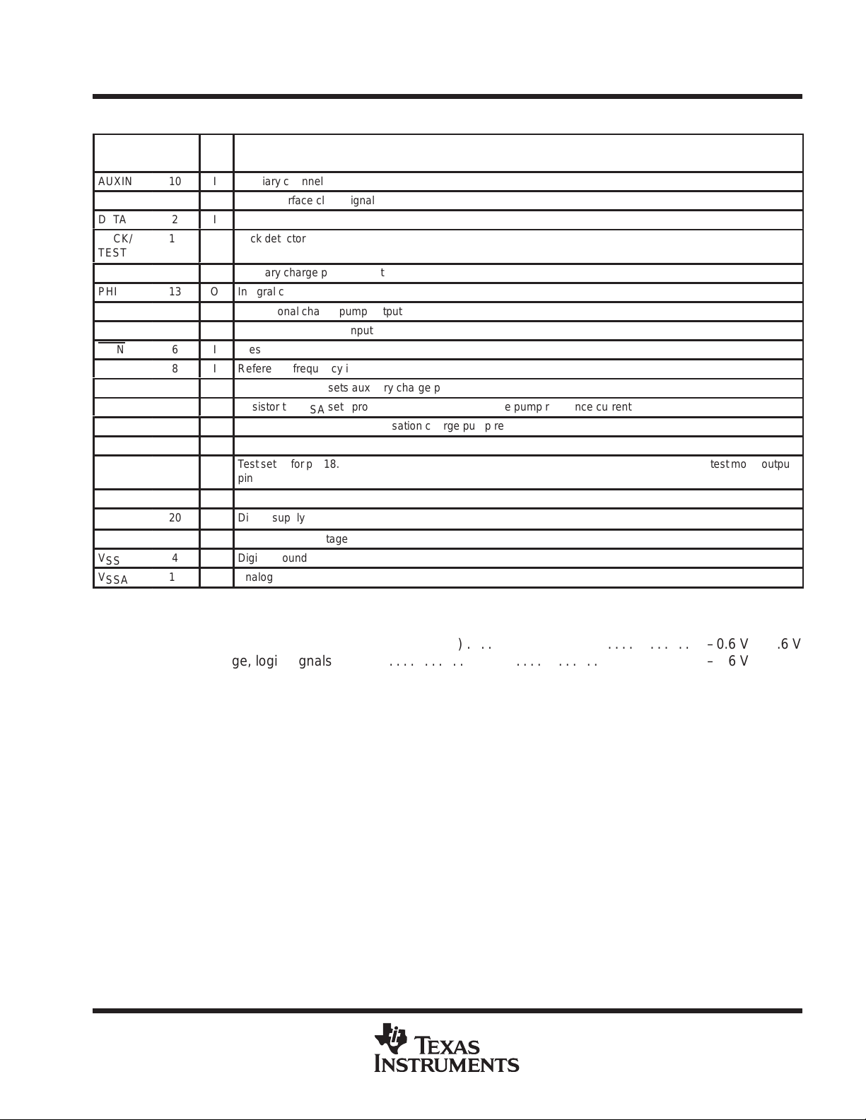
I/O
DESCRIPTION
ÁÁÁ
ÁÁÁ
ÁÁÁ
Á
ÁÁÁ
Á
ÁÁÁ
ÁÁÁ
ÁÁÁ
ÁÁÁ
ÁÁÁ
ÁÁÁ
ÁÁÁ
ÁÁÁ
Á
ÁÁÁ
Á
ÁÁÁ
ÁÁÁ
ÁÁÁ
ÁÁÁ
ÁÁÁ
TERMINAL
NAME NO.
AUXIN
CLOCK
DATA
LOCK/
TEST
ÁÁ
PHA
PHI
PHP
RFIN
RFIN
REFIN
RA
RN
RF
STROBE
TSETUP
ÁÁ
V
CCP
V
DD
V
DDA
V
SS
V
SSA
10
1
2
18
ÁÁ
11
13
14
5
6
8
9
16
17
3
19
ÁÁ
7
20
15
4
12
TRF2050
LOW-VOLTAGE 1.2-GHz FRACTIONAL-N/INTEGER-N SYNTHESIZER
SLWS030D– JUNE 1996 – REVISED OCTOBER 1998
Terminal Functions
I Auxiliary channel RF input
I Serial interface clock signal
I Serial interface data signal
O Lock detector/test mode output
O Auxiliary charge pump output
O Integral charge pump output
O Proportional charge pump output
I Prescaler positive RF input
I Prescaler negative RF input
I Reference frequency input signal
I Resistor to V
I Resistor to V
I Resistor to V
I Serial interface strobe signal
I T est setup for pin 18. For lock detect output, pin 19 connects to VCC through a pullup resistor; for test mode output,
pin 19 terminates to ground.
Prescaler positive supply voltage
Digital supply voltage
Analog supply voltage
Digital ground
Analog ground
sets auxiliary charge pump reference current
SSA
sets proportional and integral charge pump reference current
SSA
sets compensation charge pump reference current
SSA
absolute maximum ratings over operating free-air temperature range (unless otherwise noted)
Supply voltage range, V
Input voltage range, logic signals –0.6 V to 5.6 V. . . . . . . . . . . . . . . . . . . . . . . . . . . . . . . . . . . . . . . . . . . . . . . . . . . .
Operating ambient temperature range, T
Storage temperature range, T
†
Stresses beyond those listed under “absolute maximum ratings” may cause permanent damage to the device. These are stress ratings only, and
functional operation of the device at these or any other conditions beyond those indicated under “recommended operating conditions” is not
implied. Exposure to absolute-maximum-rated conditions for extended periods may affect device reliability.
NOTE 1: Voltage values are with respect to V
CCP,
VDD, V
stg
SSA
(see Note 1) –0.6 V to 5.6 V. . . . . . . . . . . . . . . . . . . . . . . . . . . . . . . . . .
DDA
A
.
–55°C to 85°C. . . . . . . . . . . . . . . . . . . . . . . . . . . . . . . . . . . . . . . . . . . .
–65°C to 150°C. . . . . . . . . . . . . . . . . . . . . . . . . . . . . . . . . . . . . . . . . . . . . . . . . . . .
†
POST OFFICE BOX 655303 • DALLAS, TEXAS 75265
3
TRF2050
LOCK/TEST
DATA, CLOCK, STROBE
Á
Á
Á
Á
Á
Á
Á
Á
Á
Á
LOW-VOLTAGE 1.2-GHz FRACTIONAL-N/INTEGER-N SYNTHESIZER
SLWS030D– JUNE 1996 – REVISED OCTOBER 1998
recommended operating conditions
MIN NOM MAX UNIT
Supply voltage, V
CCP, VDD
High-level input voltage, VIH (CLOCK, DATA STROBE) 0.7 × V
Low-level input voltage, VIL (CLOCK, DATA STROBE) –0.3 0.3 × V
Operating free-air temperature, T
, V
DDA
A
2.9
DD
4.8
VDD +0.3 V
–40 25 85 °C
5.1
DD
V
V
dc electrical characteristics VDD = V
DDA
= V
= 3.6 V, over recommended operating free-air
CCP
temperature range. internal registers: CN = 128, CL = 1, CK = 3, N = 3969, NF = 1, FMOD = 8,
SM = 0, NA = 296, SA = 0, P A = 1. external components: RN = 18 kΩ , RF = 24 kΩ, RA = 100 kΩ (unless
otherwise noted)
supply current: I = IDD + I
PARAMETER TEST CONDITIONS
I
STANDBY
I
MAIN
I
AUX
I
TOTAL
Total standby supply currents EM = EA = 0 (see Notes 2 and 3)
Operational supply currents EM = 1, EA = 0 (see Note 3)
Operational supply currents EM = 0, EA = 1 (see Note 3)
Operational supply currents
NOTES: 2. VRN = VRA = VRF = V
3. For optimum standby and operational current consumption, the following condition should be be maintained:
VDD ≤ V
DDA
digital interface
V
OH
V
OL
I
IH
I
IL
High-level output voltage
Low-level output voltage
High-level input current
Low-level input current
+ I
CCP
DDA
EM = EA = 1 (see Note 3)
DDA
< VDD + 1.
PARAMETER TEST CONDITIONS
IOH = 2 mA VDD –0.5 V
IOL = – 2 mA 0.5 V
MIN
TYP
MAX
7.0
1.5
7.5
200
UNIT
µA
mA
mA
mA
MIN TYP MAX UNIT
10 µA
10 µA
charge pump currents (see Figure 1)
auxiliary charge pump
|I
| Output current PHA
PHA
∆I
PHA
|I
|
ÁÁÁ
PHA
∆I
PHA
proportional charge pump, normal mode, VRF = V
|I
PHP-NM
∆I
|I
PHP-NM
ÁÁÁ
∆I
4
PHP-NM
PHP-NM
|
|
PARAMETER
Relative output current variation PHA (see Figure 1)
Output current matching PHA (see Figure 1)
DDA
PARAMETER
Output current PHP
Relative output current variation PHP (see Figure 1)
ББББББББББББББ
Output current matching PHP (see Figure 1)
POST OFFICE BOX 655303 • DALLAS, TEXAS 75265
TEST CONDITIONS
V
= 0.5 V
PHA
БББББÁÁÁÁ
V
PHA
= 0.5 V
DDA
DDA
TEST CONDITIONS MIN
V
= 0.5 V
PHP
БББББ
V
PHP
= 0.5 V
DDA
DDA
MIN
200
400
TYP
250
2%
TYP
500
2%
Á
MAX
300
10%
Á
±50
MAX
600
10%
Á
±50
UNIT
µA
Á
µA
UNIT
µA
Á
µA
Á
Á
Á
Á
Á
Á
Á
Á
Á
Á
Á
Á
Á
LOW-VOLTAGE 1.2-GHz FRACTIONAL-N/INTEGER-N SYNTHESIZER
charge pump currents (see Figure 1) (continued)
TRF2050
SLWS030D– JUNE 1996 – REVISED OCTOBER 1998
proportional charge pump, speed-up mode, VRF = V
PARAMETER TEST CONDITIONS MIN
|I
PHP-SM
∆I
|I
PHP-SM
∆I
integral charge pump, speed-up mode, VRF = V
|
PHP-SM
ÁÁÁ
|
PHP-SM
Output current PHP V
Relative output current variation PHP (See Figure 1)
ББББББББББББББ
Output current matching PHP (See Figure 1) V
DDA
PARAMETER TEST CONDITIONS
|I
∆I
|I
∆I
|
PHI-SM
PHI-SM
ÁÁÁ
|
PHI-SM
PHI-SM
Output current PHI V
Relative output current variation PHI (see Figure 1)
ББББББББББББББ
Output current matching PHI (see Figure 1) V
fractional compensation proportional charge pump, normal mode, V
PARAMETER TEST CONDITIONS
|I
PHP-F-NM
ÁÁÁ
Output current PHP vs fractional numerator
|
(see Note 4)
(see the section on speed-up mode operation)
DDA
TYP
PHP
PHP
= 0.5 V
= 0.5 V
DDA
DDA
2
Á
(see the section on speed-up mode operation)
MIN
TYP
V
PHP
= 0.5 V
PHI
PHI
DDA
= 0.5 V
= 0.5 V
DDA
DDA
= V
RN
DDA
, FNUM = 1
4.8
ÁÁÁ
MIN
TYP
ÁÁÁ
1.25
NOTE: 4. Fractional compensation current is proportional to the numerator content of the fractional accumulator (FNUM).
charge pump leakage currents, VRN = VRA = V
PARAMETER
I
PHP
I
PHI
I
PHA
Output current PHP
Output current PHI
Output current PHA
RF
= V
DDA
TEST CONDITIONS
V
= 0.5 V
V
V
PHP
PHI
PHA
= 0.5 V
= 0.5 V
DDA
DDA
DDA
MIN
TYP
±10
±10
±10
2.5
2%
6
2%
MAX
Á
±300
MAX
Á
±600
MAX
ÁÁÁ
MAX
10%
7.2
8%
UNIT
3
mA
Á
µA
UNIT
mA
Á
µA
UNIT
µA
UNIT
nA
ac electrical characteristics, VDD = V
main divider
PARAMETER TEST CONDITIONS
f
RFIN
V
ID_RFIN
RF input frequency
Differential RF input power
50-W single-ended characteristic impedance; ac-coupled
CCP
= V
= 3.6 V, TA = 25°C (unless otherwise noted)
DDA
MIN
TYP
–20
MAX
1.2
UNIT
GHz
0
dBm
POST OFFICE BOX 655303 • DALLAS, TEXAS 75265
5
TRF2050
Á
Á
Á
Á
Á
Á
Á
Á
Á
Á
Á
Á
Á
Á
Á
Á
Á
Á
Á
Á
Á
AUXIN
yqy( )
Á
Á
Á
Á
Á
Á
Z
AUXIN
Auxiliary in ut im edance
Z
REFIN
Reference in ut im edance
LOW-VOLTAGE 1.2-GHz FRACTIONAL-N/INTEGER-N SYNTHESIZER
SLWS030D– JUNE 1996 – REVISED OCTOBER 1998
ac electrical characteristics, VDD = V
(continued)
auxiliary divider
PARAMETER TEST CONDITIONS
ÁÁÁ
ÁÁÁ
ÁÁÁ
ÁÁÁ
f
AUXIN
ÁÁÁ
ÁÁÁ
reference divider
f
REFIN
V
I_REFIN
Auxiliary input frequency (ac-coupled)
p
p
PARAMETER TEST CONDITIONS
Reference input frequency
Reference input voltage ac-coupled
p
p
CCP
= V
= 3.6 V, TA = 25°C (unless otherwise noted)
DDA
PA = 0:
V
= VDD = 3.6 V
DDA
V
I_AUXIN
V
I_AUXIN
PA = 0:
V
= VDD = 4.8 V
DDA
V
I_AUXIN
PA = 1:
V
= VDD = 3.6 V
DDA
V
I_AUXIN
PA = 1:
V
= VDD = 4.8 V
DDA
ББББББББ
V
I_AUXIN
= 560 mVpp
= 200 mVpp
= 200 mVpp
= 200 mVpp
= 200 mVpp
MIN
TYP
MAX
Á
Á
Á
Á
Á
125
Á
70
Á
Á
ÁÁÁÁÁ
ÁÁÁÁÁ
Á
Á
Á
110
Á
40
72
5
100
3
MIN
TYP
MAX
40
200
100
3
UNIT
Á
MHz
Á
MHz
Á
MHz
Á
Á
MHz
Á
MHz
kΩ
pF
UNIT
MHz
mVpp
kΩ
pF
timing requirements, serial data interface (see Figure 2)
f
CLOCK
t
w_CLKHI
t
w_CLKLO
t
su_Data
t
h_Data
t
h_Strobe
t
su_Strobe
t
w_STRBHI
Clock frequency 10 MHz
Clock high time pulse width, CLOCK high 30 ns
Clock low time pulse width, CLOCK low 30 ns
Setup time, data valid before CLOCK↑ 30 ns
Hold time, data valid after CLOCK↑ 30 ns
Hold time, STROBE high before CLOCK↑ 30 ns
Setup time, STROBE lowafter CLOCK↑ 30 ns
STROBE high time pulse width, STROBE high
MIN MAX UNIT
50 ns
6
POST OFFICE BOX 655303 • DALLAS, TEXAS 75265
LOW-VOLTAGE 1.2-GHz FRACTIONAL-N/INTEGER-N SYNTHESIZER
PARAMETER MEASUREMENT INFORMATION
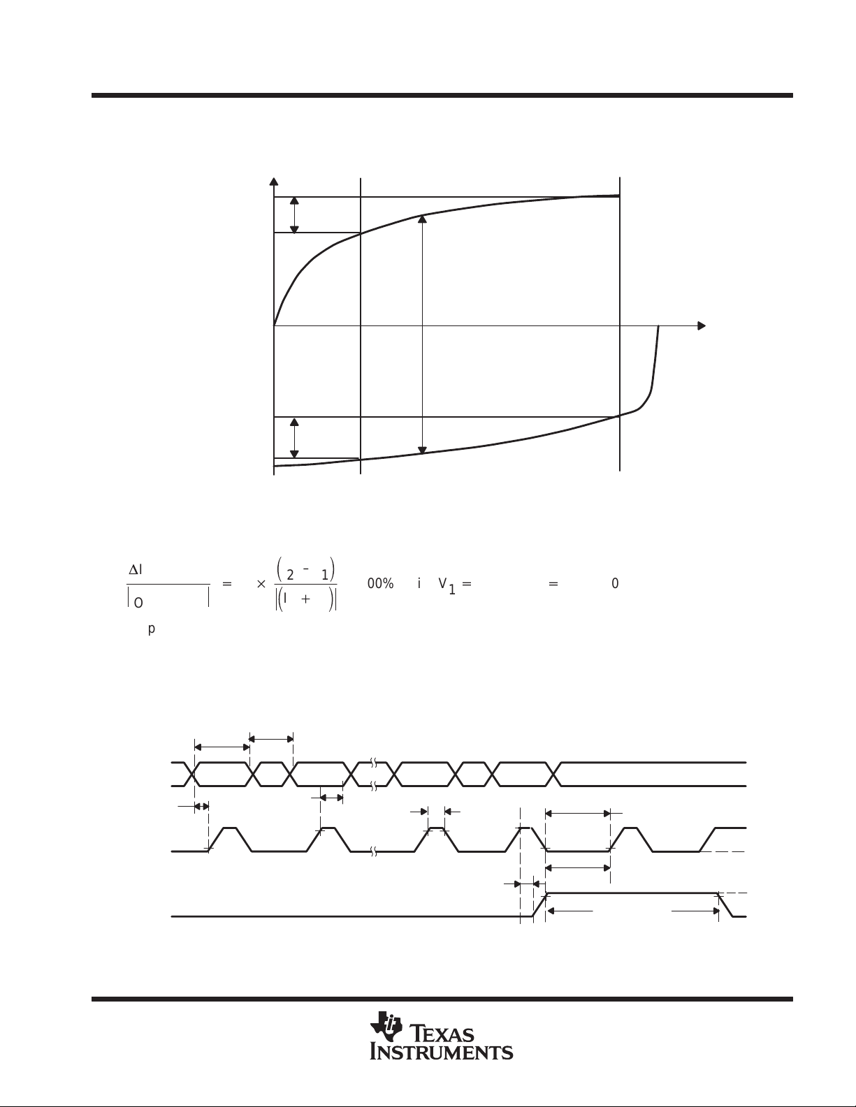
charge-pump current output definitions
Current
I
2
∆ I
REL
OUT
I
1
I
SINK
∆ I
OUT
TRF2050
SLWS030D– JUNE 1996 – REVISED OCTOBER 1998
MATCH
I
SOURCE
∆ I
OUT
REL
V
1
I
2
I
1
V
2
Voltage
Figure 1. Charge-Pump Output Current Definitions
The relative output current variation is defined as the percent difference between charge-pump current output
at two charge-pump output voltages and the mean charge-pump current output (see Figure 1):
D
I
OUT REL
Ť
I
OUT MEAN
+2
Ť
ǒ
I2–I
ǒ
Ť
I2)
Ǔ
1
×100%; with V1+
Ǔ
Ť
I
1
0.7 V, V2+
V
DDA
–0.8 V.
Output current matching is defined as the difference between charge-pump sinking current output and
charge-pump sourcing current output at a given charge-pump output (see Figure 1).
∆I
OUT MATCH
= I
SINK
– I
SOURCE
; with V1 ≤ Voltage ≤ V2.
serial-data interface timing
DATA
t
su_Data
CLOCK
STROBE
Valid
D0
Change
t
h_Data
D1
t
w_CLKHI
D30
t
su_Strobe
D31
t
w_CLKLO
t
h_Strobe
t
w_STRBHI
V
H
V
L
V
H
V
L
V
H
V
L
Figure 2. Serial-Data Interface Timing
POST OFFICE BOX 655303 • DALLAS, TEXAS 75265
7
TRF2050
LOW-VOLTAGE 1.2-GHz FRACTIONAL-N/INTEGER-N SYNTHESIZER
SLWS030D– JUNE 1996 – REVISED OCTOBER 1998
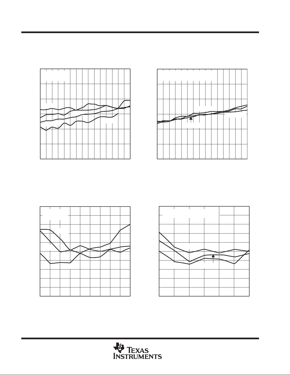
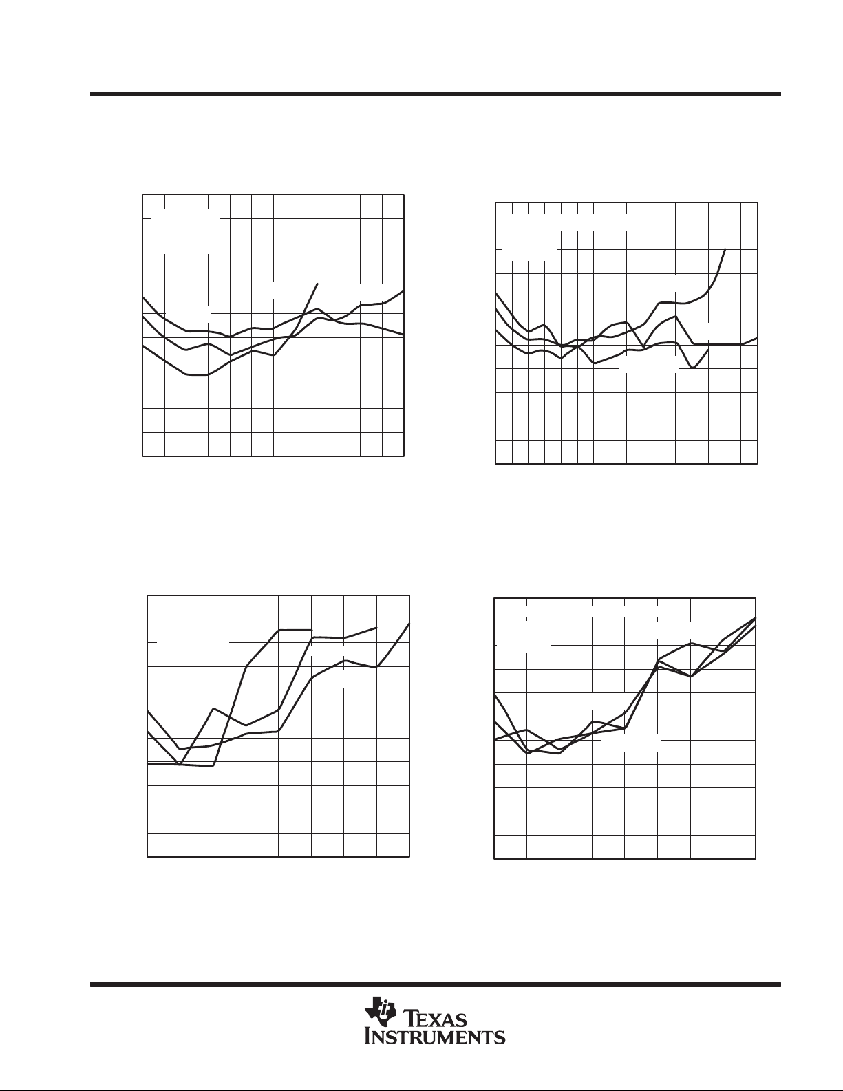
TYPICAL CHARACTERISTICS
MAIN DIVIDER INPUT POWER
FREQUENCY AND SUPPLY VOLTAGE
0
TA = 25°C
N = 4000
–10
–20
5.1 V
–30
3.6 V
–40
Main Divider Input Power – dBm
–50
–60
500
550
600
4.4 V
650
700
750
800
f – Frequency – MHz
Figure 3
vs
850
900
950
2.9 V
1000
1050
1100
1150
1200
1250
MAIN DIVIDER MINIMUM INPUT POWER
vs
FREQUENCY AND TEMPERATURE
0
V
= VDD = V
CCP
N = 4000
–10
–20
–30
–40
–50
Main Divider Minimum Input Power – dBm
–60
500
550
600
t = 25°C
650
700
f – Frequency – MHz
750
DDA
800
= 4.8 V
t = 85°C
850
900
950
Figure 4
1000
t = –40°C
1100
1050
1150
1200
1250
REFERENCE DIVIDER MINIMUM INPUT POWER
vs
FREQUENCY AND SUPPLY VOLTAGE
10
TA = 25°C
5
N = 100
0
–5
–10
–15
–20
–25
–30
–35
Reference Divider Minimum Input Power –dBm
–40
10 15 20 25 30 35 40
5.1 V
4.4 V
3.6 V
f – Frequency – MHz
Figure 5
45 50 55
REFERENCE DIVIDER MINIMUM INPUT POWER
vs
FREQUENCY AND TEMPERATURE
10
V
= VDD = V
CCP
NR = 100
5
0
–5
–10
–15
–20
t = 85°C
–25
–30
–35
Reference Divider Minimum Input Power – dBm
–40
10 20 30 40 50 60 70
t = –40°C
f – Frequency – MHz
DDA
= 4.8 V
t = 25°C
Figure 6
8
POST OFFICE BOX 655303 • DALLAS, TEXAS 75265
TRF2050
LOW-VOLTAGE 1.2-GHz FRACTIONAL-N/INTEGER-N SYNTHESIZER
SLWS030D– JUNE 1996 – REVISED OCTOBER 1998
TYPICAL CHARACTERISTICS
AUXILIARY DIVIDER MINIMUM INPUT POWER
vs
FREQUENCY AND SUPPLY VOLTAGE
5
TA = 25°C
0
PA = 1
–5
N = 100
–10
–15
–20
–25
–30
–35
–40
–45
Auxiliary Divider Minimum Input Power – dBm
–50
5.1 V
51525
10 20 30 40 50 60
f – Frequency – MHz
3.6 V
35 45 55 65
Figure 7
AUXILIARY DIVIDER MINIMUM INPUT POWER
vs
FREQUENCY AND SUPPLY VOLTAGE
5
TA = 25°C
0
PA = 0
NA = 100
–5
–10
–15
–20
–25
–30
–35
–40
Auxiliary Divider Minimum Input Power – dBm
–45
–50
5 50 100
3.6 V
25 75 125 175
f – Frequency – MHz
4.4 V
5.1 V
Figure 9
4.4 V
150 200
AUXILIARY DIVIDER MINIMUM INPUT POWER
vs
FREQUENCY AND TEMPERATURE
5
V
= VDD = V
CCP
0
PA = 1
N = 100
–5
–10
–15
–20
–25
–30
–35
–40
–45
Auxiliary Divider Minimum Input Power – dBm
–50
10 15 20 25 35 40 45
530
f – Frequency – MHz
DDA
= 4.8 V
t = –40°C
t = 85°C
50 55 60 65 70 75
Figure 8
AUXILIARY DIVIDER MINIMUM INPUT POWER
vs
FREQUENCY AND TEMPERATURE
5
V
= VDD = V
CCP
0
PA = 0
N = 100
–5
–10
–15
–20
–25
–30
–35
–40
–45
Auxiliary Divider Minimum Input Power – dBm
–50
25 50 100 150 175
5 75 125 200
= 4.8 V
DDA
t = –40°C
t = 85°C
t = 25°C
f – Frequency – MHz
Figure 10
t = 25°C
80
85
POST OFFICE BOX 655303 • DALLAS, TEXAS 75265
9
TRF2050
LOW-VOLTAGE 1.2-GHz FRACTIONAL-N/INTEGER-N SYNTHESIZER
SLWS030D– JUNE 1996 – REVISED OCTOBER 1998
TYPICAL CHARACTERISTICS
CH1 S
1 µFS 2: 37.43 Ω –160.98 Ω 1.0245 pF
11
965.000 000 MHz
2
1
3
START 500.000 MHz STOP 1 400.000 MHz
Figure 11. Typical RFIN Impedance (S11)
1: 89.063 Ω
–272.88 Ω
500 MHz
3: 16.773 Ω
–127.36 Ω
1.4 GHz
10
POST OFFICE BOX 655303 • DALLAS, TEXAS 75265
TRF2050
LOW-VOLTAGE 1.2-GHz FRACTIONAL-N/INTEGER-N SYNTHESIZER
SLWS030D– JUNE 1996 – REVISED OCTOBER 1998
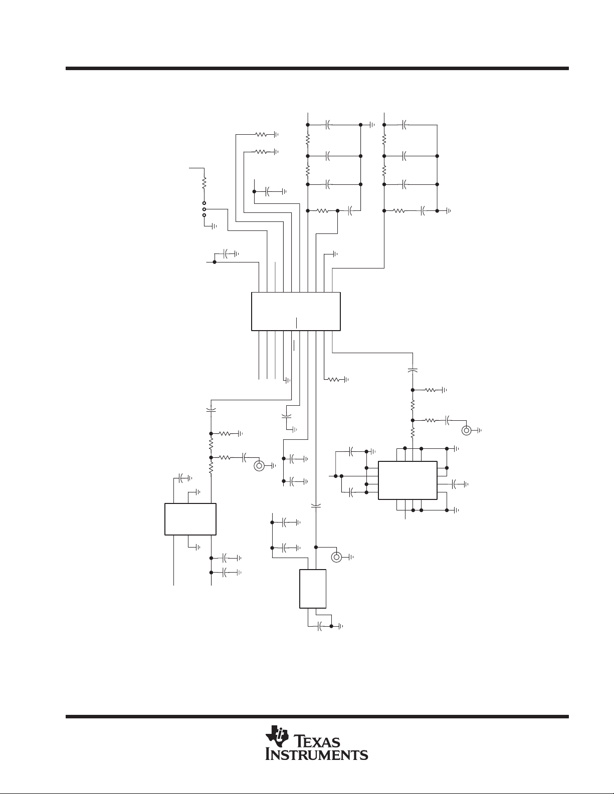
APPLICATION INFORMATION
6
M_VCO
1
MOD
VT
MVT
VDD
JP1
µ.1 F
C7
5
GND
GND
2
R9
10 k
Lock
31
Test
VDD
C8
100 pF
R10
18
R11
R15
18
R12
4
MQE001
VCC OUT
3
VOSC1
C5
49.9
18
C26
C30
R14
30 k
R13
18 k
VDDA
C10
µ.1 F
VDD
TSETUPRFRN
201918171615141312
VDD
TSET
U1
CLK
DATA
123456789
DTA
CLK
C39
100 pF
J1
22 pF
1000 pF
F
µ.1
LOCK/TEST
RF
LOCK
STRB
VSS
AGND
STRB
C9
VDD
VOSC3
C33
C34
MVT
C16
180 pF
R19
3.9 k
C17
470 pF
R20
12 k
C18
1200 pF
9.1 k
VSSA
VSSA
RA
RA
VOSC2
µ.022 F
PHA
11
PHA
AUX
10
AUX
R16
110 k
J3
NDK_OSC
C21
TRF2050
R22
VDDA
PHP
PHI
RN
PHI
PHP
VDDA
REF
VCCP
RFIN
RFIN
REF
VDD
RFIN
RFIN
100 pF
µ1F
C38
+
µ.1 F
C11
C23
1000 pF
22 pF
3
OUT
VCC
TCXO
VCONT
GND
2
14
µ.039 F
C31
1000 pF
C31
22 pF
AVT
0
R18
R17
12 k
121110
GND
13141516
VCC
GND
GND
123
AUX1_VCO
VCO190–S
C16
DNP
C14
180 pF
C13
47 pF
R21
36 k
C24
18
R23
R24
OUT
GND
GND
GNDVTGND
AVT
18
9
4
C19
220pF
GND
GND
1800 pF
R25
49.9
R26
18
GND
GND
MOD
GND
C43
220pF
5678
C20
J2
µ.1 F
µ.1 F
C22
Figure 12. Evaluation Board Schematic (Part 1 of 2)
POST OFFICE BOX 655303 • DALLAS, TEXAS 75265
11

TRF2050
LOW-VOLTAGE 1.2-GHz FRACTIONAL-N/INTEGER-N SYNTHESIZER
SLWS030D– JUNE 1996 – REVISED OCTOBER 1998
APPLICATION INFORMATION
VOSC3
5
6
8
VO
VO
NC
VR6
VT
VO
VO
ANC
2
173
4
270
R37
LM317LBD
R38
µ1F
C37
+
390
VDD
µ.1 F
VR5
VR4
VR3
VR2
VOSC2
8
NC
VT
173
VOPTO
8
NC
VT
173
VOSC1
8
NC
VT
173
VDD
8
NC
VT
173
C36
5
6
C35
6
C32
6
C28
6
VO
VO
4
µ.1 F
5
VO
VO
4
µ.1 F
5
VO
VO
4
µ.1 F
5
VO
VO
4
ANC
ANC
ANC
ANC
R4
LM317LBD
R35
R3
LM317LBD LM317LBDLM317LBD LM317LBD
R2
VO
VO
2
VO
VO
2
VO
VO
2
VO
VO
2
STROBE
DATA
LOCK/TEST
R34
1.8 k
VOPTO
R30
2.7 k
R33
R29
R32
R28
R31
6.2 k
1.8 k
6.2 k
1.8 k
6.2 k
STROBE
DATA
CLOCK
U3
5
1
6
U2
5
1
2
4
4N28S
U4
5
1
6
4
2
4N28S
LOCK/TEST
1
2
6
U5
4
5
6
4
2
4N28S
CLOCK
MOC8030
270
270
270
220
W
2
R8
R36
R7
µ1F
C5
+
820
µ1F
C25
+
820
µ1F
C4
+
620
µ1F
C3
+
CW
3
R6
1 k
1
12
R27
1.8 k
LOCK
DATA
CLOCK
STROBE
11421531641751861972082192210231124122513
Figure 12. Evaluation Board Schematic (Part 2 of 2)
POST OFFICE BOX 655303 • DALLAS, TEXAS 75265
POWER
SUPPLY
VR1
+
VDDA
8
NC
VT
173
C1
GND
2
µ4.7 F
HUB
C29
6
VO
VO
C32
DGND
µ.1 F
5
VO
VO
4
µ.1 F
ANC
AGND
HUBGND
VDDA VDD
R1
220
W
2
µ1F
C2
+
CW
3
R5
1 k
1
Note: Evaluation board dc supply circuitry and PC interface only

TRF2050
LOW-VOLTAGE 1.2-GHz FRACTIONAL-N/INTEGER-N SYNTHESIZER
SLWS030D– JUNE 1996 – REVISED OCTOBER 1998
APPLICATION INFORMATION
Table 1. TRF2050 Evaluation Board Parts List
DESIGNATORS DESCRIPTION VALUE QTY
C1 Capacitor 4.7 uF 1 “A” 3.2x1.6 Venkel TA010TCM475KAR
C2, 3, 4, 5, 25,
37, 38
C6, 7, 10, 11, 20,
22, 27, 28, 29,
32, 35, 36
C8, 9, 39 Capacitor 100 pF 3 0603 1.6x.08 Murata GRM39COG series
C13 Capacitor 47 pF 1 0603 1.6x.08 Murata GRM39COG series
C14, 16 Capacitor 180 pF 2 0603 1.6x.08 Venkel C0603COG series
C15 Capacitor Not Used 0603 1.6x.08 Not Used
C17 Capacitor 470 pF 1 0603 1.6x.08 Murata GRM39X7R series
C18 Capacitor 1200 pF 1 0603 1.6x.08 Murata GRM39X7R series
C12, 30, 33 Capacitor 1000 pF 3 0603 1.6x.08 Murata GRM39X7R series
C19 Capacitor 1800 pF 1 0603 1.6x.08 Venkel C0603X7R series
C21 Capacitor .039 pF 1 1210 3.2x2.5 Panasonic ECH–U1H393JB
C23 Capacitor .022 uF 1 0603 1.6x.08 Murata GRM39X7R series
C24, 40 Capacitor 220 pF 2 0603 1.6x.08 Murata GRM39X7R series
C26, 31, 34 Capacitor 22 pF 3 0603 1.6x.08 Murata GRM39COG series
R1, 2 Resistor 220
R3, 4, 35, 37 Resistor 270
R5, 6 Resistor 1 k
R7 Resistor 620
R8, 36 Resistor 820
R9 Resistor 10 k
R10, 25 Resistor 49.9
R11, 12, 15,
23, 24, 26
R13 Resistor 18 k
R14 Resistor 30 k
R16 Resistor 110 k
R17, 20 Resistor 12 k
R18 Resistor 0
R19 Resistor 3.9 k
R21 Resistor 36 k
R22 Resistor 9.1 k
R27, 28, 29, 34 Resistor 1.8 k
R30 Resistor 2.7 k
R31, 32, 33 Resistor 6.2 k
R38 Resistor 390
U1 Integrated circuit 1 TI TRF2050
U2, 3, 4 Optoelectronics 3 730C–04 Motorola 4N28S
Capacitor 1.0 uF 7 “A” 3.2x1.6 Venkel TA025TCM105KAR
Capacitor 0.1 uF 12 0603 1.6x.08 Murata GRM39Y5V104Z016
Resistor 18
W
W
W
W
W
W
W
W
W
W
W
W
W
W
W
W
W
W
W
W
2 0603 1.6x.08 Panasonic ERJ–3GSYJ221
4 0603 1.6x.08 Panasonic ERJ–3GSYJ271
2 .25” square Bourns 3269W001102
1 0603 1.6x.08 Panasonic ERJ–3GSYJ series
2 0603 1.6x.08 Panasonic ERJ–3GSYJ series
1 0603 1.6x.08 Panasonic ERJ–3GSYJ series
2 0603 1.6x.08 Panasonic ERJ–3EKF49R9
6 0603 1.6x.08 Panasonic ERJ–3GSYJ series
1 0603 1.6x.08 Panasonic ERJ–3GSYJ series
1 0603 1.6x.08 Panasonic ERJ–3GSYJ series
1 0603 1.6x.08 Panasonic ERJ–3GSYJ series
2 0603 1.6x.08 Panasonic ERJ–3GSYJ series
1 0603 1.6x.08 Venkel CR0603–16W–000J1
1 0603 1.6x.08 Panasonic ERJ–3GSYJ series
1 0603 1.6x.08 Panasonic ERJ–3GSYJ series
1 0603 1.6x.08 Panasonic ERJ–3GSYJ series
4 0603 1.6x.08 Panasonic ERJ–3GSYJ series
1 0603 1.6x.08 Panasonic ERJ–3GSYJ series
3 0603 1.6x.08 Panasonic ERJ–3GSYJ series
1 0603 1.6x.08 Panasonic ERJ–3GSYJ series
SIZE
(mm)
MANUFACTURER
MANUFACTURER
P/N
POST OFFICE BOX 655303 • DALLAS, TEXAS 75265
13

TRF2050
LOW-VOLTAGE 1.2-GHz FRACTIONAL-N/INTEGER-N SYNTHESIZER
SLWS030D– JUNE 1996 – REVISED OCTOBER 1998
APPLICATION INFORMATION
Table 1. TRF2050 Evaluation Board Parts List (Continued)
DESIGNATORS DESCRIPTION VALUE QTY
U5 Optoelectronics 1 730C–04 Motorola MOC8030S
VR1, 2, 3, 4, 5, 6 Voltage regulator 6 SO–8
P1 Para. connector 1 AMP 747238–4
J1, 2, 3 SMA connector 3 EF Johnson 142–0701–831
TP1 to TP8 T est point Assorted 8 Components Corp. TP–105–01 series
Main VCO
TCXO
AUX VCO
Voltage-controlled
oscillator
Temp.-compensated
crystal oscillator
Voltage-controlled
oscillator
ATTEN 10 dB
RL 0 dBm
MKR
D
1.00 kHz
D
–48.83 dB
1 Murata MQE001
1 Toyocom TCO–980
1 Vari-L Comp. VCO190–S
VAVG 10
10 dB/
SIZE
(mm)
MANUFACTURER
National
Semiconductor
MANUFACTURER
P/N
LM317LM
14
CENTER 926.66977 MHz
RBW 100 Hz VBW 100 Hz
SPAN 10.00 kHz
SWP 802 ms
Figure 13. Close-in Noise at 926.67 MHz; MODULO – 8; NF = 1; CN = 64
POST OFFICE BOX 655303 • DALLAS, TEXAS 75265

TRF2050
LOW-VOLTAGE 1.2-GHz FRACTIONAL-N/INTEGER-N SYNTHESIZER
SLWS030D– JUNE 1996 – REVISED OCTOBER 1998
APPLICATION INFORMATION
ATTEN 10 dB
RL 0 dBm
MKR
D
30.0 kHz
D
–63.17 dB
CENTER 914.1900 MHz
RBW 1 kHz VBW 1 kHz
Figure 14. Fractional Spurs, f
ATTEN 10 dB
RL 0 dBm
VAVG 25
10 dB/
SPAN 100.00 kHz
SWP 250 ms
= 914.19 MHz; MODULO – 8; NF = 1; CN = 64
VCO
VAVG 25
10 dB/
MKR
D
30.0 kHz
D
–63.34 dB
CENTER 939.1500 MHz
RBW 1 kHz VBW 1 kHz
Figure 15. Fractional Spurs, f
SPAN 100.00 kHz
SWP 250 ms
= 939.15 MHz; MODULO – 8; NF = 1; CN = 64
VCO
POST OFFICE BOX 655303 • DALLAS, TEXAS 75265
15

TRF2050
LOW-VOLTAGE 1.2-GHz FRACTIONAL-N/INTEGER-N SYNTHESIZER
SLWS030D– JUNE 1996 – REVISED OCTOBER 1998
APPLICATION INFORMATION
ATTEN 10 dB
RL 0 dBm
MKR
D
30.0 kHz
D
–64.16 dB
CENTER 914.3700 MHz
RBW 1 kHz VBW 1 kHz
Figure 16. Fractional Spurs, f
ATTEN 10 dB
RL 0 dBm
VAVG 25
10 dB/
SPAN 100.00 kHz
SWP 250 ms
= 914.37 MHz; MODULO – 8; NF = 7; CN = 64
VCO
VAVG 25
10 dB/
MKR
D
30.0 kHz
D
–63.50 dB
CENTER 939.3300 MHz
RBW 1 kHz VBW 1 kHz
Figure 17. Fractional Spurs, f
SPAN 100.0 kHz
SWP 250 ms
= 939.33 MHz; MODULO – 8; NF = 7; CN = 64
VCO
16
POST OFFICE BOX 655303 • DALLAS, TEXAS 75265

LOW-VOLTAGE 1.2-GHz FRACTIONAL-N/INTEGER-N SYNTHESIZER
SLWS030D– JUNE 1996 – REVISED OCTOBER 1998
PRINCIPLES OF OPERATION
serial programming input
The TRF2050 internal registers are programmed using a three-wire (CLOCK, DA TA, STROBE) serial interface.
The serial data is structured into 24-bit standard-length or 32-bit long-length words of which one or four bits are
dedicated address bits. The flag LONG in the D-Word determines whether the A0 (LONG = 0) or A1
(LONG = 1) format is applicable. Figures 18 and 19 show the format of the serial data for two modes of TRF2050
operation: SA7025 and EPM, respectively. The least significant bit (LSB) of the C-Word determines the
operational mode of the TRF2050: 0 = SA7025, 1 = EPM.
In SA7025 mode, the TRF2050 emulates the Philips SA7025 with respect to serial programming.
Microcontroller software written for the SA7025 works transparently when the TRF2050 is operated in SA7025
emulation mode.
Figure 2 shows the timing diagram of the serial input. When the STROBE signal is low, the signal on the DAT A
input is clocked into a shift register on the positive edges of the CLOCK. When the STROBE signal is high,
depending on the 1 or 4 address bit(s), the data is latched into different working registers or temporary registers.
In order to fully program the synthesizer, four words must be sent: D, C, B, and A. The E-Word is for testing
purposes only.
TRF2050
The A-Word contains new data for the main divider. The A-Word is loaded only when a main divider
synchronization signal is also active. This is done to avoid phase jumps during reprogramming the main divider.
The synchronization signal is generated by the main divider.
When the TRF2050 is operated in SA7025 emulation mode, programming the A-Word sets the main charge
pumps, which are located on outputs PHP and PHI, into speed-up mode, as long as the STROBE is high. When
the TRF2050 is operated in EPM mode, speed-up mode duration is determined by field G in the B-Word.
NOTE:
The C-Word must be sent during the first programming cycle after power-up
in order to set the mode of operation (7025 or EPM).
POST OFFICE BOX 655303 • DALLAS, TEXAS 75265
17

TRF2050
LOW-VOLTAGE 1.2-GHz FRACTIONAL-N/INTEGER-N SYNTHESIZER
SLWS030D– JUNE 1996 – REVISED OCTOBER 1998
PRINCIPLES OF OPERATION
WORD
MSB (Last In)
D31
A1
D23 D0
A0
B
C
NM1NF0 CN
NM1NF0
CN1 000 0000 CK CL PR
NA1 001 0P0000
NM3 NM2
NM3 NM2
A
NM2
NM2
LSB (First In)
D0
PR = 01
PR = 10
MS
F
M
D
1 11 T
E
1
NR1 010
RESERVED
SET TO ZERO
E
SM SA
M
O
E
O
N
A
D
G
Figure 18. Serial Word Format for SA7025 Emulation Mode
L
18
POST OFFICE BOX 655303 • DALLAS, TEXAS 75265

Á
Á
Á
Á
Á
Á
Á
Á
Á
Á
Á
Á
Á
Á
Á
TRF2050
LOW-VOLTAGE 1.2-GHz FRACTIONAL-N/INTEGER-N SYNTHESIZER
SLWS030D– JUNE 1996 – REVISED OCTOBER 1998
PRINCIPLES OF OPERATION
T able 2. SA7025 Emulation Serial-Word-Format Function Listing
SYMBOL
CK
CL
CN
EA
ÁÁÁ
BITS FUNCTION
4 Binary acceleration factor for integral charge pump current
2 Binary acceleration factor for proportional charge pump current
8 Binary current-setting factor for main charge pumps
1 Auxiliary divider enable flag:
ÁÁÁÁ
0 = disabled
1 = enabled
EM 1 Main divider enable flag:
ÁÁÁ
0 = disabled
1 = enabled
FMOD
ÁÁÁ
ÁÁÁ
LONG
1 Fractional-N modulus selection:
ÁÁÁÁ
ÁÁÁÁ
0 = modulo 5
1 = modulo 8
1 A word format selection:
0 = 24-bit A0 format
ÁÁÁ
ÁÁÁÁ
1 = 32-bit A1 format
MS 2 Mode select
00 = 7025 Emulation Mode
NA 12 Auxiliary divider ratio
NF
NM1
NM2
ÁÁÁ
NM3
3 Fractional-N increment
12 Number of main divider cycles when prescaler modulus = 64
8 if PR = 01
4 if PR = 10
ÁÁÁÁ
Number of main divider cycles when prescaler modulus = 65
4 if PR = 10 Number of main divider cycles when prescaler modulus = 72
NR 12 Reference divider ratio
PA 1 Auxiliary prescaler select:
ÁÁÁ
ÁÁÁ
PR
2 Prescaler type:
0 = divide by 4
1 = divide by 1
PR = 01; modulus 2 prescaler (64/65)
ÁÁÁ
ÁÁÁÁ
PR = 10; modulus 3 prescaler (64/65/72)
SA 2 Reference select for auxiliary phase detector
SM 2 Reference select for main phase detector
T 2 Test mode connection of internal signals to the LOCK terminal:
00 = ACCU overflow
01 = Auxiliary divider
10 = Main divider
11 = Reference divider
POST OFFICE BOX 655303 • DALLAS, TEXAS 75265
19

TRF2050
LOW-VOLTAGE 1.2-GHz FRACTIONAL-N/INTEGER-N SYNTHESIZER
SLWS030D– JUNE 1996 – REVISED OCTOBER 1998
PRINCIPLES OF OPERATION
MSB (Last In) LSB (First In)
WORD
D23
D0
A0
B
C
D
E
1 111
NNF0
G
CN1 000 CK CL
NA1 001
NR1 010
RESERVED
SET TO ZERO
P
A
SM SA
FMOD
E
MA
E
0
A
M
C
C
P
P
MS
00
T
Figure 19. Serial Word Format for Extended Performance Mode (EPM)
20
POST OFFICE BOX 655303 • DALLAS, TEXAS 75265

Á
Á
Á
Á
Á
Á
Á
Á
Á
Á
Á
Á
Á
Á
Á
Á
Á
Á
Á
TRF2050
LOW-VOLTAGE 1.2-GHz FRACTIONAL-N/INTEGER-N SYNTHESIZER
SLWS030D– JUNE 1996 – REVISED OCTOBER 1998
PRINCIPLES OF OPERATION
Table 3. Extended Performance Mode Function Table
ÁÁÁ
SYMBOL
ÁÁÁ
BITS
Á
Á
SAME AS
ÁÁ
SA7025
MODE
ÁÁ
FUNCTION
Auxiliary charge polarity:
ACP
ÁÁÁ
CK
CL
CN
EA
1
Á
4
2
8
1
No
ÁÁ
Yes Binary acceleration factor for integral charge pump current
Yes Binary acceleration factor for proportional charge pump current
Yes Binary current setting factor for main charge pumps
0 = positive
1 = negative
Auxiliary divider enable flag:
0 = disabled
ÁÁÁ
Á
ÁÁ
1 = enabled
Main divider enable flag:
EM
ÁÁÁ
FMOD
G
1 Yes
Á
5 No Fraction accumulator modulus
4
No Speed-up mode duration (See Table 9)
0 = disabled
1 = enabled
Main charge pump polarity:
MCP
ÁÁÁ
MS
N
NA
NF
NR
1
Á
2
18
12
4
No
ÁÁ
No
No Overall main divider integer division ratio (NM)
Yes Auxiliary divider ratio
No Fractional-N increment
12 Yes Reference divider ratio
0 = positive
1 = negative
Mode select
01 = Extended Performance Mode
Auxiliary prescaler select:
PA
ÁÁÁ
1 Yes
Á
0 = divide by 4
1 = divide by 1
SA 2 Yes Reference select for auxiliary phase detector
SM
2 Yes Reference select for main phase detector
T 2 Yes Test mode connection of internal signals to the LOCK terminal:
00 = ACCU overflow
01 = Auxiliary divider
10 = Main divider
11 = Reference divider
POST OFFICE BOX 655303 • DALLAS, TEXAS 75265
21

TRF2050
LOW-VOLTAGE 1.2-GHz FRACTIONAL-N/INTEGER-N SYNTHESIZER
SLWS030D– JUNE 1996 – REVISED OCTOBER 1998
PRINCIPLES OF OPERATION
main divider – general (see Figure 20)
The differential RFIN inputs are amplified to internal ECL logic levels and provide excellent sensitivity (better
than –20 dBm at 1 GHz), making the prescaler ideally suited for direct interface with a VCO. The internal
dual-modulus (32/33) prescaler and counter sections divide the VCO frequency down to the reference phase
detector frequency . The prescaler division ratio (÷32 or ÷33) is controlled by a feedback signal that is a function
of the 18-bit N-field counters. The N-field counter section is composed of two separate counters: a 5-bit
A-Counter and a 13-bit B-Counter. The prescaler divides by 33 until the A-Counter reaches terminal count and
then divides by 32 until the B-Counter reaches terminal count, whereupon both counters reset and the cycle
repeats. The following equation relates the total N division as a function of the 32/33 prescaler:
N
= 32 (B – A) + 33(A), where 0 ≤ A ≤ 31, and 31 ≤ B ≤ 8191.
Total
It is not necessary to determine the values of A and B in the equation above; simply program the N field with
the total division ratio desired (fractional effects ignored).
The N-division ratio has a range of 992 ≤ N
RFIN
Structure of N-Word
A B
5 Bits 13 Bits
LSB MSB
N
4
NF
FMOD
5
32/33 Prescaler
N
18
5-Bit
Fraction Accumulator
≤ 262143.
Total
13-Bit
B-Counter
5-Bit
A-Counter
5
18-Bit Register
18
18-Bit
Adder
to Phase Detector
13
Figure 20. Main Divider Organization
main divider – SA7025 emulation
The internal triple modulus prescaler configuration of the SA7025 provides for prescaler division ratios of
64/65/72. The TRF2050 has internal conversion logic that allows the TRF2050 to emulate the SA7025 main
divider operation. When operated in SA7025 emulation mode, the TRF2050 is programmed using the SA7025
serial interface format shown in Figure 18. The TRF2050 internal conversion is transparent and need not be
considered under normal use, thereby allowing use of existing SA7025 programming codes without change.
The following equations relate the total N-division as a function of the emulated 64/65 dual-modulus and
64/65/72 triple-modulus prescalers:
N
= 64 (NM1 + 2) + 65 (NM2), where PR = 01 and
Total
N
= 64 (NM1 + 2) + 65 (NM2) + 72 (NM3 + 1), where PR = 10.
Total
22
POST OFFICE BOX 655303 • DALLAS, TEXAS 75265

LOW-VOLTAGE 1.2-GHz FRACTIONAL-N/INTEGER-N SYNTHESIZER
SLWS030D– JUNE 1996 – REVISED OCTOBER 1998
PRINCIPLES OF OPERATION
For contiguous channels, the following rules must be observed:
For PR = 01: 61 ≤ NM1 ≤ 4095 and 0 ≤ NM2 ≤ 63, which yields minimum and maximum divide ratios of 4032
and 266303, respectively.
For PR = 10: 14 ≤ NM1 ≤ 4095 and 0 ≤ NM2 ≤ 15, and 0 ≤ NM3 ≤ 15, which yields minimum and maximum divide
ratios of 1096 and 264335, respectively.
main divider – synchronization
The A-Word is loaded only when a main divider synchronization signal is active. This prevents phase jumps
when reprogramming the main divider. The synchronization signal is generated by the main divider, and it is
active while the main divider is counting down from the programmed value. When the main divider reaches its
terminal count, a main divider output pulse is sent to the main phase detector. Also at this time, the loading of
the A-Word is disabled. Therefore, to correctly load the new A-Word, the STROBE signal must be active high
for at least a minimum number of VCO input cycles at RFIN.
main divider – fractional accumulator
The TRF2050 main synthesizer loop can operate as a traditional integer-N feedback PLL or as a fractional-N
feedback PLL. The integer-N feedback loop divides the VCO frequency by integer values of N, which results
in phase detector reference comparisons at the desired channel spacing. A fractional-N feedback loop divides
the VCO frequency by an integer term plus a fractional term, which results in phase detector reference
comparisons at integer multiples of the desired system channel spacing.
TRF2050
Integer-N division: VCO frequency N = phase detector reference frequency
= channel spacing
Fractional-N division: VCO Frequency (N + NF/FMOD) = phase detector reference frequency
= FMOD × channel spacing
where 0 ≤ NF < FMOD and 1 ≤ FMOD ≤ 16.
Because the main counter and prescaler sections cannot divide by a fraction of an integer, the fractional-N
division is accomplished by averaging main divider cycles by N and N+1. A fractional accumulator is
programmed with values of NF and FMOD to control the main counter and prescaler sections to divide by N
or N+1.
The fractional accumulator operates modulo FMOD and is incremented by NF at the completion of each main
divider cycle. When the fractional accumulator overflows, division by N+1 occurs. Otherwise, the main counters
and prescaler divide by N; division by N+1 is transparent to the user. Table 4 shows the contents of the fractional
accumulator and the resulting N or N+1 division for two fractional division ratios.
POST OFFICE BOX 655303 • DALLAS, TEXAS 75265
23

TRF2050
LOW-VOLTAGE 1.2-GHz FRACTIONAL-N/INTEGER-N SYNTHESIZER
SLWS030D– JUNE 1996 – REVISED OCTOBER 1998
PRINCIPLES OF OPERATION
Table 4. Fractional Accumulator Operation
NF = 3, FMOD = 8 NF = 6, FMOD = 8
ACCUMULATOR
NUMERATOR
3 ÷ N 6
6
1 ÷ N + 1, overflow 2
4
7
2
5
0
STATE
÷ N
÷ N
÷ N
÷ N + 1, overflow
÷ N
÷ N + 1, overflow
For example, suppose that a typical AMPS channel of 953.25 MHz is desired. Because AMPS channel spacing
is 30 kHz, for fractional-N operation the main phase detector reference frequency must be a multiple of 30 kHz;
240 kHz is typical. A value of FMOD = 8 is selected because 240 kHz / 30 kHz = 8. Dividing the channel frequency
by the reference frequency results in 953.13 ÷ 240 kHz = 3971.375 = 3971 + 3/8. This example is shown in
T able 4 where NF = 3 and FMOD = 8. The table shows that over the period of a complete fractional accumulator
cycle, the fractional accumulator overflows three times for every eight main divider cycles. Figure 21 illustrates
the division by N or N+1 for this 3/8 fractional channel example.
Number of Main
Divider Pulses
N
(3971)
N
(3971)
N + 1
(3972)
ACCUMULATOR
NUMERATOR
N
(3971)
4
0
6
4
2
0
N
(3971)
STATE
÷ N
÷ N + 1, overflow
÷ N + 1, overflow
÷ N + 1, overflow
÷ N
÷ N + 1, overflow
÷ N + 1, overflow
÷ N + 1, overflow
N + 1
(3972)
N
(3971)
(3972)
N + 1
RF Input
Main Divider Out
Figure 21. 3/8 Fractional Channel Main Divider Operation
The mean division over the complete fractional accumulator cycle as shown in Figure 21 is:
N
MEAN
3971)3971)3972)3971)3971)3972)3971)3972
+
+
3971)3ń8
8
Therefore, fractional channels are available every 30 kHz or 240 kHz
1
FMOD
240 kHz
+
+
3971.375
8
.
main divider – integer channels
In the case where NF = 0, only division by N occurs, and the fractional accumulator is essentially in a steady
state with a numerator of 0. It never increments or overflows. A channel that requires NF = 0 is a pure integer
channel because the fractional term of
NF
FMOD
is zero.
24
POST OFFICE BOX 655303 • DALLAS, TEXAS 75265

LOW-VOLTAGE 1.2-GHz FRACTIONAL-N/INTEGER-N SYNTHESIZER
SLWS030D– JUNE 1996 – REVISED OCTOBER 1998
PRINCIPLES OF OPERATION
main divider – fractional-N sidebands and compensation
Programming a fractional-N channel means the main divider and prescaler divide by N or N + 1 as dictated by
the operation of the fractional accumulator. Because the main divider operation is integer in nature and the
desired VCO frequency is not, the output of the main phase detector is modulated with a resultant fractional-N
phase ripple that produces sideband energy if left uncompensated. This phase ripple is proportional and
synchronized to the contents of the fractional accumulator that is used to control fractional-N sideband
compensation. Only channels that require a nonzero value of NF have the fractional-N sideband energy. The
fractional-N sidebands, which appear at offset frequencies from the VCO fundamental tone, are multiples of
NF/FMOD. Figure 22 shows the fractional-N phase detector ripple for a 3/8 fractional channel.
240 kHz
Main Phase
Detector Reference
Main Phase
Detector VCO
Feedback
TRF2050
Detector Fractional-N
Main Phase
Ripple
Fractional
Accumulator State
036147250
Figure 22. Fractional-N Phase Detector Ripple for 3/8 Channel
The TRF2050 has internal circuitry that provides a means to compensate for the phase detector fractional-N
phase ripple, thereby significantly reducing the magnitude of the fractional-N sidebands. Because the current
waveform output of the main PLL proportional charge pumps is modulated with the phase detector fractional-N
phase ripple, a fractional-N compensation charge-pump output is summed with the main PLL proportional
charge pump.
Figure 23 shows the fractional-N ripple magnitude on the main PHP charge-pump output. The magnitude is
essentially constant, and the pulse width is modulated with the contents of the fractional accumulator. The area
under the main PHP charge-pump curve represents the amount of charge delivered to the loop filter network.
In order to minimize fractional-N sidebands in the VCO spectrum, the compensation current waveform is
generated to have
equal
and
opposite
sign magnitude
area
to the main PHP charge pump.
POST OFFICE BOX 655303 • DALLAS, TEXAS 75265
25

TRF2050
LOW-VOLTAGE 1.2-GHz FRACTIONAL-N/INTEGER-N SYNTHESIZER
SLWS030D– JUNE 1996 – REVISED OCTOBER 1998
PRINCIPLES OF OPERATION
Accumulator State
Fractional
Main PHP Charge Pump
Fractional-N Ripple
Magnitude
Compensation Charge
Pump Fractional-N
Ripple Magnitude
036147250
Pulse-Width
mA
µA
Modulation
Pulse-Amplitude
Modulation
Figure 23. Main PHP and Compensation Charge Pump Fractional-N Waveforms for 3/8 Channel
The compensation waveform is pulse-amplitude modulated with the contents of the fractional accumulator. The
main PHP pulse magnitude is much larger than the compensation pulse magnitude but the compensation pulse
has a much longer duration than that of the main PHP pulse. The compensation pulse is optimally centered
about the main PHP charge pump pulse in order to avoid additional sideband energy due to the phase offset
between the main and compensation pulses.
The following example illustrates a method for determining correct values for RN, RF, and CN for minimal
fractional-N sidebands based on VCO frequency and reference frequency.
Assumptions:
The main VCO is locked on channel.
953 MHz ± 10 MHz main VCO operation, 942.99 – 962.91 MHz
19.44 MHz reference frequency
240 kHz phase detector reference frequency
500 µA peak main PHP current
1. Determine the fundamental fractional-N pulse width portion of the main PHP charge-pump output waveform
for the lower, upper, and mean frequencies.
Frac
Frac
Frac
PW–MEAN
PW–LWR
PW–UPR
+
+
+
1
f
PD
1
f
PD
Frac
N
–
f
VCO
N
–
f
VCO
PW*LWR
+
240 kHz
+
240 kHz
)
2
1
1
Frac
PW–UPR
3929
–
942.99 MHz
4012
–
962.91 MHz
+
132.557 ps,
+
129.815 ps,
132.557 ps)129.815 ps
+
2
+
131.186 ps.
The mean-unit pulse width of the fractional-N portion of the main PHP charge-pump output waveform over
the VCO frequencies of interest is 131.186
ps
. This fundamental pulse width is modulated by the contents
of the fractional accumulator. For the 3/8 fractional-N channel example, the pulse width varies as shown
in Table 5.
26
POST OFFICE BOX 655303 • DALLAS, TEXAS 75265

LOW-VOLTAGE 1.2-GHz FRACTIONAL-N/INTEGER-N SYNTHESIZER
SLWS030D– JUNE 1996 – REVISED OCTOBER 1998
PRINCIPLES OF OPERATION
Table 5. Main PHP Fractional-N Pulse-Widths and Areas for 3/8 Channel
NF = 3, FMOD = 8
ACCUMULATOR
STATE
3 3 x
6 6 x
1 1 x
4 4 x
7 7 x
2 2 x
5 5 x
0 0 x
Table 5 also shows the area of the fractional-N portion of the main PHP charge-pump waveform.1
2. Determine the pulse width of the compensation charge-pump output waveform.
MAIN PHP FRACTIONAL PULSE WIDTH
PW–Mean
PW–Mean
PW–Mean
PW–Mean
PW–Mean
PW–Mean
PW–Mean
PW–Mean
(ps)
= 393.558 393.558 ps x 500 µA = .196779
= 787.116 787.116 ps x 500 µA = .393558
= 131.186 131.186 ps x 500 µA = .065593
= 524.744 524.744 ps x 500 µA = .262372
= 918.302 918.302 ps x 500 µA = .459151
= 262.372 262.372 ps x 500 µA = .131186
= 655.930 655.930 ps x 500 µA = .327965
= 0 0 ps x 500 µA = 0
MAIN PHP FRACTIONAL AREA
TRF2050
(ps X AMPS)
Comp
PW
+
f
Ref
1
+
1
19.44 MHz
+
51.440 ns
3. Determine the fundamental compensation charge-pump current magnitude using the fundamental main
PHP fractional area.
Comp
Mag
+
Frac
Comp
Area
PW
0.065593 psA
+
51.440 ns
+
1.275mA
Table 6 shows the magnitude of the compensation pulse as a function of the fractional accumulator.
Table 6. Compensation Pulse Magnitudes for 3/8 Channel
NF = 3, FMOD = 8
Accumulator
Numerator
3 3 x 1.275 = 3.825
6 6 x 1.275 = 7.651
1 1 x 1.275 = 1.275
4 4 x 1.275 = 5.101
7 7 x 1.275 = 8.926
2 2 x 1.275 = 2.550
5 5 x 1.275 = 6.376
0 0 x 1.275 = 0
Compensation Pulse
Magnitude (µA)
4. Using the result of step 3, determine the value of RF to give the fundamental compensation pulse
magnitude.
RF(k
W)+
Comp
25
Mag
(
)
m
A
25
+
1.275
POST OFFICE BOX 655303 • DALLAS, TEXAS 75265
+
19.6 kW.
27

TRF2050
LOW-VOLTAGE 1.2-GHz FRACTIONAL-N/INTEGER-N SYNTHESIZER
SLWS030D– JUNE 1996 – REVISED OCTOBER 1998
PRINCIPLES OF OPERATION1234
5. Determine the values of CN and RN for the main PHP charge-pump peak current of 500 µA. Assume that
a midrange value of CN equals 128.
ǒ
RN(k
W)+
6. The value of the fundamental compensation pulse magnitude calculated in step 3 is fixed and the
compensation pulse width calculated in step 2 is also fixed. However, because the VCO can tune over a
significant range of frequencies, the pulse width of the fractional-N portion of the main PHP charge-pump
waveform varies; thus, the area of the same waveform varies. In order to maintain equal areas under the
fractional-N portion of the main PHP charge-pump and compensation waveforms, CN must vary with the
VCO frequency . As the VCO frequency increases, the fractional-N portion of the main PHP charge-pump
waveform pulse width decreases proportionally, thereby decreasing the area under the same waveform.
Therefore, CN is adjusted to equalize the main PHP and compensation waveform areas, as follows:
Frac
PW-LWR
Frac
PW-UPR
The fundamental area of the fractional-N portion of the main PHP charge-pump waveform (step 1) is
calculated as 0.065593 picosecond x amperes. If you calculate the fundamental area of the fractional-N
portion of the main PHP charge-pump waveform using the actual pulse widths above in place of the average
pulse width calculated in step 1, the fractional-N main PHP areas is obtained as follows:
Frac
Area-L WR
Frac
Area-UPR
The actual areas under the fractional-N portion of the main PHP waveform require slight modification in the
charge-pump current. The variation of CN required for area equalization is determined using a simple ratio
form:
CN
LWR
CN
UPR
18.75
= 132.557 ps for f
= 129.815 ps for f
= 132.557 ps – 0.500 mA = 0.066279 ( ps × amps)
= 129.815 ps – 0.500 mA = 0.064691 (ps × amps)
Frac
+
Frac
Frac
+
Frac
CN
256
Area–AVG
Area–UPR
Area–AVG
Area–UPR
1
Ǔ
)
I(mA
= 942.99 MHz
VCO
= 962.91 MHz
VCO
CN
AVG
CN
AVG
– 0.75
+
+
+ǒ18.75
0.065593
0.066279
0.065593
0.064691
128
256
128+126
128+130
0.5 mA
1
Ǔ
– 0.75+18 k
W
Therefore, for this example, CN can vary from 126-130 over the VCO frequency range of 942.99 – 962.91
MHz for optimum fractional-N sideband suppression. Due to component and circuit tolerances, additional
deviations in CN may be appropriate.
auxiliary divider
The input signal on AUXIN is amplified by a single-ended, ac-coupled input buffer/amplifier that has sufficient
sensitivity (200 mVpp at 200 MHz) for direct connection to a typical VCO. The 12-bit (NA) auxiliary divider
incorporates a divide by 1 (P A = 1) or divide by 4 (PA = 0) prescaler . The total division ratio can be expressed
as:
N
= 4 x NA where PA = 0
Total
N
= NA, where PA = 1 and NA = 4 to 4095
Total
28
POST OFFICE BOX 655303 • DALLAS, TEXAS 75265

LOW-VOLTAGE 1.2-GHz FRACTIONAL-N/INTEGER-N SYNTHESIZER
SLWS030D– JUNE 1996 – REVISED OCTOBER 1998
PRINCIPLES OF OPERATION
reference divider
The input signal on REFIN is amplified by a single-ended, ac-coupled input buffer/amplifier that has sufficient
sensitivity (300 mVpp at 50 MHz) for direct connection to a typical TCXO. The 12-bit (NR) reference divider total
division ratio can be expressed as:
N
= NR, where NR = 4 to 4095
Total
A four-section postscaler is connected to the output of the reference divider section. The main and auxiliary
synthesizer sections can individually select a reference postscaler division of 1, 2, 4, or 8 by programming fields
SM and SA, respectively (see Figure 24).
MAIN SELECT
SM = “00”
TRF2050
Reference Input
Divide by NR
SM = “01”
SM = “10”
SM = “11”
÷ 2 ÷ 2 ÷ 2
AUXILIARY SELECT
SA = “11”
SA = “10”
SA = “01”
SA = “00”
Main Phase
Detector
Auxiliary
Phase Detector
Figure 24. Reference Divider
phase detectors
The main and auxiliary synthesizer sections (see Figure 25) incorporate dual D-type flip-flop phase-frequency
detectors (PFD). A PFD has gain with a phase error over a range of ±2π and exhibits an infinite pull-in range.
Dead-band compensation about zero-phase error is provided by forcing the sourcing and sinking charge pumps
to have a minimum on-time of 1/f
The phase detectors can be programmed for polarity sense. Normally , external system VCOs have a positive
slope control-voltage frequency characteristic. Some VCOs have a negative slope characteristic. The TRF2050
main and auxiliary phase detectors can be programmed for use with positive or negative slope VCOs using the
MCP
and
ACP
fields, respectively, in the B-Word (EPM mode).
when the loop is operating in a locked condition.
Ref
For positive slope VCOs: MCP = ACP = 0
For negative slope VCOs: MCP = ACP = 1
POST OFFICE BOX 655303 • DALLAS, TEXAS 75265
29

TRF2050
LOW-VOLTAGE 1.2-GHz FRACTIONAL-N/INTEGER-N SYNTHESIZER
SLWS030D– JUNE 1996 – REVISED OCTOBER 1998
PRINCIPLES OF OPERATION
SET
D
1
Q
VDDA
REFIN
REFIN or AUXIN
Reference Divider
/NR
Main or Auxiliary
Reference Divider
/N or /NR
Q
CLR
SET
CLR
Q
Q
VSSA
1
D
Charge Pump
Output
Figure 25. Main and Auxiliary Phase Detector Circuit
charge-pump current plans
The TRF2050 uses internal band-gap references and external resistors to develop biasing reference currents
for the various charge pumps sections. Three terminals are designated for the external resistors: RN, RF, and
RA. Internal, programmable coefficients CN, CL, and CK are also used. T able 7 shows how the external resistors
are used to achieve desired charge-pump peak currents.
Table 7. Charge Pump Current Plans
PARAMETER MODE CONDITION UNIT
x
x
Ǔ
CN
256
CN
Ǔ
256
xCKx2
CL)1
Ǔ
Peak proportional, normal mode current PHP
Peak proportional, speed-up mode current
18.75
PHP
PK*SM
Peak integral, speed-up mode current PHI
†
Peak compensation, normal mode current
Peak auxiliary current PHAPK+
†
The compensation charge
Divider – Fractional-N Sidebands and Compensation.
ǒ
+
RN)0.75
CN
Ǔ)ǒ
x
256
1.25
ǒ
RA
-pump current is a pulse-amplitude modulated with the contents of the fractional accumulator. See the section on Main
PK*NM
18.75
RN)0.75
PK*SM
CompPK+
Ǔ
x20
+
x
256
ǒ
+
RN)0.75
30
RF
18.75
ǒ
RN)0.75
CN
x2
18.75
CL)1
The average charge-pump current for the PHP, PHI, and PHA terminals is defined by:
q
+
error
2
p
xIPK.
I
AVG
Normal RN in kΩ mA
Speed-up RN in kΩ mA
Speed-up RN in kΩ mA
Normal RF in kΩ µA
Normal RA in kΩ mA
30
POST OFFICE BOX 655303 • DALLAS, TEXAS 75265

LOW-VOLTAGE 1.2-GHz FRACTIONAL-N/INTEGER-N SYNTHESIZER
SLWS030D– JUNE 1996 – REVISED OCTOBER 1998
PRINCIPLES OF OPERATION
loop enable/disable
The main and auxiliary loops can be enabled and disabled by the contents of the enable bits EM and EA,
respectively. When disabled, all currents in the RF input stages are switched off; the bias currents for the
respective charge-pump circuits are switched off as well. When both loops are disabled (EM = EA = 0), the
reference input stage currents are switched off. The reference chain can be turned off because the serial
interface operates independent of the reference input for the loading of serial words.
Table 8. Loop Enable/Disable
EM EA ENABLED DISABLED
0 0 Main, Auxiliary , Reference
0 1 Auxiliary, Reference Main,
1 0 Main, Reference Auxiliary
1 1 Main, Auxiliary, Reference
speed-up mode
TRF2050
When the main synthesizer frequency is changed, it may be desirable to increase the loop bandwidth for a short
time in order to achieve a faster lock time. The proportional charge-pump current is increased and the integral
charge-pump current is switched on for the duration of speed-up mode. The section,
plans
, illustrates how the charge-pump currents are a function of the external resistor RN and the programmable
coefficients CN, CL, and CK.
The duration of the speed-up mode is determined by the operational mode of the TRF2050 device: enhanced
performance mode (EPM) or SA7025 emulation mode. In EPM mode, the speed-up mode duration is controlled
as a function of the G field in the B-Word and the reference frequency divider period.
Table 9. Speed-Up Mode
G VALUE DURATION
0–14 [(G+1) × NR × SM × 16]/f
15 < (NR ×SM)/(f
When the TRF2050 is operated in SA7025 emulation mode, the speed-up mode duration is a function of the
STROBE signal associated with the A-Word. When the STROBE signal followed by an A-Word write transaction
goes active, the speed-up mode currents begin and persist until the STROBE signal is returned to an inactive
state.
REFIN
REFIN
× 2); which is less than 1/2 a phase detector cycle
EPM
charge-pump current
lock detect
The lock condition of the PLL is defined as a phase difference of less than a ±1 cycle on the reference input
REFIN. The LOCK terminal can be polled to determine the synthesizer lock condition of either or both loops.
The lock detect function is described by the Boolean expression:
LOCK
+
ǒ
LD
Main
)
EM
Ǔ·ǒ
LD
Aux
POST OFFICE BOX 655303 • DALLAS, TEXAS 75265
)
EA
Ǔ
31

TRF2050
LOW-VOLTAGE 1.2-GHz FRACTIONAL-N/INTEGER-N SYNTHESIZER
SLWS030D– JUNE 1996 – REVISED OCTOBER 1998
test modes
The LOCK terminal may be used for test operations by terminating pin 19 to ground. When test modes are
enabled, the LOCK
ones to the two LSBs of the E-Word. Test modes are disabled by terminating pin 19 to V
resistor of 10 kΩ.
T1 T0 MODE
0 0 Buffered output of the fractional accumulator
0 1 Buffered output of the auxiliary divider
1 0 Buffered output of the main divider
1 1 Buffered output of the reference divider
The test mode can be used to verify the division ratio of the reference divider, the auxiliary divider , and the main
divider and prescaler.
terminal is connected to internal nodes of the TRF2050. T est modes are enabled by writing
through a pull-up
CC
Table 10. Test Modes
32
POST OFFICE BOX 655303 • DALLAS, TEXAS 75265

TRF2050
LOW-VOLTAGE 1.2-GHz FRACTIONAL-N/INTEGER-N SYNTHESIZER
SLWS030D– JUNE 1996 – REVISED OCTOBER 1998
MECHANICAL DATA
PW (R-PDSO-G**) PLASTIC SMALL-OUTLINE PACKAGE
14 PIN SHOWN
0,65
14
1
1,20 MAX
A
7
0,10 MIN
0,32
0,19
8
6,70
4,50
4,30
6,10
M
0,13
Seating Plane
0,10
0,15 NOM
Gage Plane
0,25
0°–8°
0,75
0,50
PINS **
DIM
A MAX
A MIN
NOTES: A. All linear dimensions are in millimeters.
B. This drawing is subject to change without notice.
C. Body dimensions do not include mold flash or protrusion not to exceed 0,15.
D. Falls within JEDEC MO-153
8
3,10
2,90
14
5,10
4,90
16
5,10
20
6,60
6,404,90
24
7,90
7,70
28
9,80
9,60
4040064/D 10/95
POST OFFICE BOX 655303 • DALLAS, TEXAS 75265
33

IMPORTANT NOTICE
T exas Instruments and its subsidiaries (TI) reserve the right to make changes to their products or to discontinue
any product or service without notice, and advise customers to obtain the latest version of relevant information
to verify, before placing orders, that information being relied on is current and complete. All products are sold
subject to the terms and conditions of sale supplied at the time of order acknowledgement, including those
pertaining to warranty, patent infringement, and limitation of liability.
TI warrants performance of its semiconductor products to the specifications applicable at the time of sale in
accordance with TI’s standard warranty. Testing and other quality control techniques are utilized to the extent
TI deems necessary to support this warranty . Specific testing of all parameters of each device is not necessarily
performed, except those mandated by government requirements.
CERT AIN APPLICATIONS USING SEMICONDUCTOR PRODUCTS MAY INVOLVE POTENTIAL RISKS OF
DEATH, PERSONAL INJURY, OR SEVERE PROPERTY OR ENVIRONMENTAL DAMAGE (“CRITICAL
APPLICATIONS”). TI SEMICONDUCTOR PRODUCTS ARE NOT DESIGNED, AUTHORIZED, OR
WARRANTED TO BE SUITABLE FOR USE IN LIFE-SUPPORT DEVICES OR SYSTEMS OR OTHER
CRITICAL APPLICA TIONS. INCLUSION OF TI PRODUCTS IN SUCH APPLICATIONS IS UNDERST OOD TO
BE FULLY AT THE CUSTOMER’S RISK.
In order to minimize risks associated with the customer’s applications, adequate design and operating
safeguards must be provided by the customer to minimize inherent or procedural hazards.
TI assumes no liability for applications assistance or customer product design. TI does not warrant or represent
that any license, either express or implied, is granted under any patent right, copyright, mask work right, or other
intellectual property right of TI covering or relating to any combination, machine, or process in which such
semiconductor products or services might be or are used. TI’s publication of information regarding any third
party’s products or services does not constitute TI’s approval, warranty or endorsement thereof.
Copyright 1999, Texas Instruments Incorporated
 Loading...