

D
Wide VHF/UHF Frequency Range
200 MHz to 450 MHz for World-Wide
Remote Control Frequency Compatibility
D
High Receiver Sensitivity ... –103 dBm at
315 MHz
D
Accepts Baseband Data Rates From 500 Hz
to 10 kHz
D
Manchester-Decoded and Raw Baseband
Outputs for Easy Interface to Serial Data
Decoders and Microcontrollers
D
TRF (Tuned Radio Frequency) Design
Eliminates Local Oscillator (No Emissions)
and Reduces Many Government Type
Approvals (Including FCC)
D
Adjustable Internal Sampling Clock Set By
External Components
description
TRF1400
RF TELEMETRY RECEIVERS
VHF/UHF RZ ASK REMOTE CONTROL RECEIVER
SLWS014E – JUNE 1996 – REVISED APRIL 1998
D
Internal Amplifier and Comparator for
Amplification and Shaping of Low-Level
Input Signals With Average-Detecting
Autobias Adaptive Threshold Circuitry for
Improved Sensitivity
D
Minimum External Component Count and
Surface-Mount Packaging for Extremely
Small Circuit Footprint – Typically Replaces
More Than 40 Components in an Equivalent
Discrete Solution
D
No Manual Alignment When Using SAW
Filters
D
Advanced Submicron BiCMOS Process
Technology for Minimum Power
Consumption
The TRF1400 VHF/UHF RZ ASK remote control
receiver is specifically designed for RZ ASK
(return-to-zero amplitude-shift keyed) communications systems operating in the 200-MHz to
450-MHz band. This device is targeted for use in
automotive and home security systems, garage
door openers, remote utility metering, and other
low-power remote control and telemetry systems.
A complete RZ ASK receiver solution on a chip,
the TRF1400 requires only a minimum of external
components for operation. This significantly
reduces the complexity and footprint of new
designs compared with current discrete receiver
designs. The TRF1400 requires no manual
LPF
AGND
RFIN3
A VCC
AGND
A VCC
AGND
OFFSET
AGND
OSCR
OSCC
DVCC
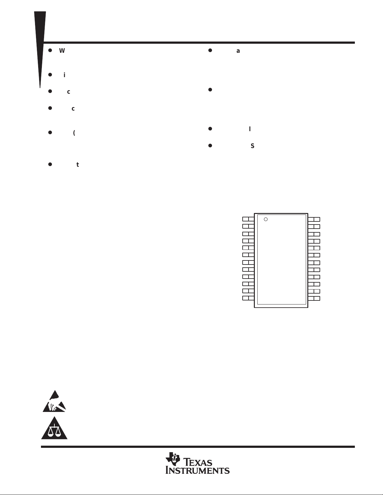
DW PACKAGE
(TOP VIEW)
1
2
3
4
5
6
7
8
9
10
11
12
24
23
22
21
20
19
18
17
16
15
14
13
RFOUT2
LNA2T
RFIN2
AGND
RFOUT1
LNA1T
RFIN1
AGND
DOUT
TRIG
BBOUT
DGND
alignment when using external SAW (surface
acoustic wave) filters. For a lower-cost solution,
the device is also compatible with external LC
components.
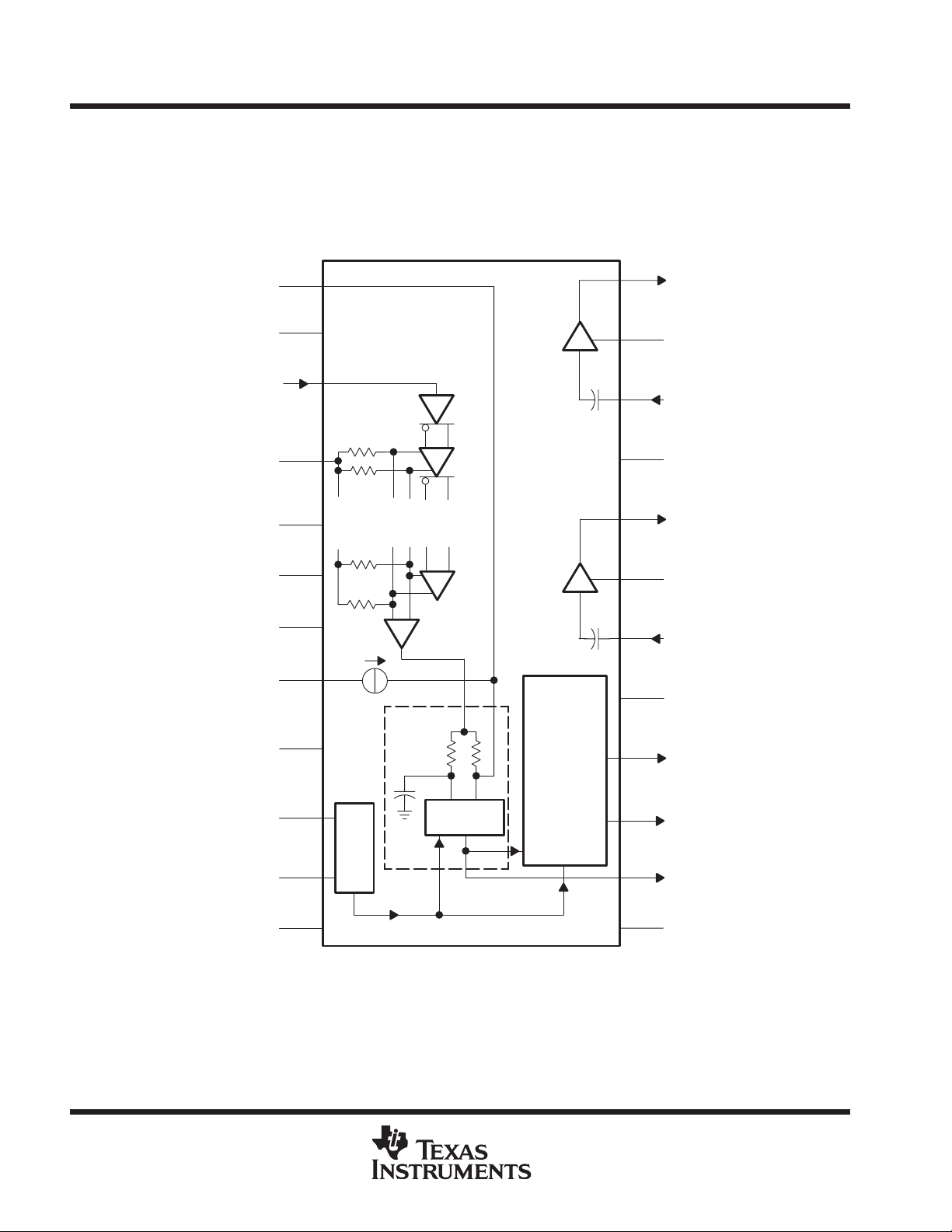
The TRF1400 also includes several on-chip features that normally require additional circuitry in a receiver
system design. These include two low-noise front-end amplifiers, an RF amplifier/comparator for detection and
shaping of input signals, and a demodulated RZ ASK baseband TTL-level output that readily interfaces to
self-synchronizing devices. Also included is on-chip Manchester decoding logic that provides a specially
formatted TTL data output, synchronized with a trigger output, for easy interface to any microcontroller using
Manchester-encoded data.
These devices have limited built-in ESD protection. The leads should be shorted together or the device placed in conductive foam
during storage or handling to prevent electrostatic damage to the MOS gates.
Please be aware that an important notice concerning availability, standard warranty, and use in critical applications of
Texas Instruments semiconductor products and disclaimers thereto appears at the end of this data sheet.
PRODUCTION DATA information is current as of publication date.
Products conform to specifications per the terms of Texas Instruments
standard warranty. Production processing does not necessarily include
testing of all parameters.
POST OFFICE BOX 655303 • DALLAS, TEXAS 75265
Copyright 1998, Texas Instruments Incorporated
1
TRF1400
RF TELEMETRY RECEIVERS
VHF/UHF RZ ASK REMOTE CONTROL RECEIVER
SLWS014E – JUNE 1996 – REVISED APRIL 1998
description (continued)
The TRF1400 VHF/UHF RZ ASK remote control receiver is available in a 24-pin SOIC (DW) package, and is
characterized for operation over the temperature range of –40°C to 85°C. The DW package is available taped
and reeled; add R suffix to device type when ordering (e.g., TRF1400DWR).
functional block diagram
LPF
AGND
RFIN3
AVCC
AGND
AVCC
AGND
OFFSET
AGND
OSCR
1
2
3
4
Six Log-Detecting
5
RF Amp Stages
6
7
8
9
10
Summing
Amp
Auto Level
Comparator
+–
LNA2
LNA1
Manchester
Decoding
Logic
24
23
22
21
20
19
18
17
16
15
RFOUT2
LNA2T
RFIN2
AGND
RFOUT1
LNA1T
RFIN1
AGND
DOUT
TRIG
Clock
OSCC
DVCC
2
11
12
POST OFFICE BOX 655303 • DALLAS, TEXAS 75265
SCLK
14
13
BBOUT
DGND

I/O
DESCRIPTION
TRF1400
RF TELEMETRY RECEIVERS
VHF/UHF RZ ASK REMOTE CONTROL RECEIVER
SLWS014E – JUNE 1996 – REVISED APRIL 1998
Terminal Functions
TERMINAL
NAME NO.
AGND 2, 5,
7, 9,
17, 21
AVCC 4, 6 Positive power supply voltage for all analog circuits — 4.5 V to 5.5 V
BBOUT 14 O Baseband data output. BBOUT is the demodulated envelope of the recovered RF signal and is active with any
DGND 13 Digital ground for all internal logic circuits. DGND is not internally connected to analog ground (AGND).
DOUT 16 O Data output. Data appearing at DOUT is a binary, TTL representation of the baseband data, and is only meaningful
DVCC 12 Positive power supply voltage for all digital circuits. DVCC is 4.5 V to 5.5 V . For best noise performance, DVCC
LNA1T 19 Low-noise amplifier (LNA) 1 ground termination. LNA1T should be connected to AGND through a parallel
LNA2T 23 Low-noise amplifier (LNA) 2 ground termination. LNA2T should be connected to AGND through a parallel
LPF 1 Connection for external low-pass capacitor used in the average-detecting adaptive threshold circuitry.
OFFSET 8 Connection for external offset resistor. A resistor (1 MΩ suggested) sets the internal threshold detector offset
OSCC 11 Internal oscillator frequency-setting capacitor. A capacitor , connected between OSCC and ground, in conjunction
OSCR 10 Internal oscillator frequency-setting resistor. A resistor , connected between OSCR and OSCC, in conjunction with
RFIN1 18 I RF input to first low-noise, high-gain amplifier stage
RFIN2 22 I RF input to second low-noise, high-gain amplifier stage
RFIN3 3 I RF input to the detecting RF amplifier stages. Filtered RF in the form of AM RZ ASK data at frequencies between
RFOUT1 20 O RF output of the first low-noise, high-gain amplifier
RFOUT2 24 O RF output of the second low-noise, high-gain amplifier. Typically, the input of an external SAW or LC filter is
TRIG 15 O Trigger output. TRIG pulses to indicate each new received data cell and is only meaningful when
Analog ground for all internal analog circuits. AGND is not internally connected to digital ground (DGND). All
analog signals are referenced to AGND.
received ASK signal coding format.
when Manchester-encoded ASK data is received. DOUT is active high and is internally pulled down.
should connect to AVCC at the power supply, not at the TRF1400 device.
resistor-capacitor bias network. If left unconnected, LNA1 is disabled.
resistor-capacitor bias network. If left unconnected, LNA2 is disabled.
voltage. Lowering the value of this resistor decreases device sensitivity .
with a resistor connected between OSCR and OSCC, determines the speed of the internal clock oscillator (SCLK).
The SCLK signal is used for processing the demodulated incoming data stream and controls the Manchester
decoding and timing recovery logic sections of the device. The internal oscillator must be set to 10 times the
received Manchester data rate for valid TRIG and DOUT, or to 5 times the received baseband data rate.
a capacitor connected between OSCC and ground determines the speed of the internal oscillator (SCLK). The
SCLK signal is used for processing the demodulated incoming data stream and controls the Manchester decoding
and timing recovery logic sections of the device. The internal oscillator must be set to 10 times the received
Manchester data rate for valid TRIG and DOUT, or to 5 times the received baseband data rate.
200 MHz and 450 MHz, at a baud rate between 500 Hz and 10 kHz can be applied to RFIN3 for detection and
decoding.
connected to RFOUT2.
Manchester-encoded ASK data is received. TRIG is active high and is internally pulled down.
POST OFFICE BOX 655303 • DALLAS, TEXAS 75265
3
TRF1400
DOUT, TRIG, BBOUT
RF TELEMETRY RECEIVERS
VHF/UHF RZ ASK REMOTE CONTROL RECEIVER
SLWS014E – JUNE 1996 – REVISED APRIL 1998
absolute maximum ratings over operating free-air temperature range (unless otherwise noted)
†
Supply voltage range, AVCC, DVCC (see Note 1) –0.6 to 6 V. . . . . . . . . . . . . . . . . . . . . . . . . . . . . . . . . . . . . . . .
Input voltage range, V
–0.6 to 6 V. . . . . . . . . . . . . . . . . . . . . . . . . . . . . . . . . . . . . . . . . . . . . . . . . . . . . . . . . . . . . . .
I
Continuous total power dissipation 180 mW. . . . . . . . . . . . . . . . . . . . . . . . . . . . . . . . . . . . . . . . . . . . . . . . . . . . . . . .
Operating free-air temperature range, T
Storage temperature range, T
–65°C to 150°C. . . . . . . . . . . . . . . . . . . . . . . . . . . . . . . . . . . . . . . . . . . . . . . . . . .
stg
–55°C to 85°C. . . . . . . . . . . . . . . . . . . . . . . . . . . . . . . . . . . . . . . . . . . .
A
ESD protection, all terminals: human body model 2 kV. . . . . . . . . . . . . . . . . . . . . . . . . . . . . . . . . . . . . . . . . . . . .
machine model 200 V. . . . . . . . . . . . . . . . . . . . . . . . . . . . . . . . . . . . . . . . . . . . . . .
JEDEC latchup 150 mA or 11 V. . . . . . . . . . . . . . . . . . . . . . . . . . . . . . . . . . . . . . . . . . . . . . . . . . . . . . . . . . . . . . . . . .
†
Stresses beyond those listed under “absolute maximum ratings” may cause permanent damage to the device. These are stress ratings only, and
functional operation of the device at these or any other conditions beyond those indicated under “recommended operating conditions” is not
implied. Exposure to absolute-maximum-rated conditions for extended periods may affect device reliability.
NOTE 1: Voltage values are with respect to GND.
recommended operating conditions
MIN NOM MAX UNIT
Supply voltage, V
Input frequency, f
Operating free-air temperature, T
Minimum permissible AM modulation of RF envelope applied to RF Input, measured at –101 dBm 25%
CC
in
A
4.5 5.5 V
200 450 MHz
–40 85 °C
electrical characteristics as measured in the test circuit detailed in Figures 1 through 6 with
= 315 MHz over recommended ranges of supply voltage and operating free-air temperature,
f
in
typical values are at V
= 5 V and TA = 25°C (unless otherwise noted)
CC
current consumption
PARAMETER TEST CONDITIONS MIN TYP MAX UNIT
I
Average supply current from V
CC
CC
I/O pins terminated with typical loads,
Signal applied with a 5-kHz baseband data rate
I/O pins terminated with typical loads,
Signal applied with a 2.5-kHz Manchester data rate
I/O pins terminated with typical loads, no data input 2.5
2.7 3.5
2.7 3.5
mA
digital interface
PARAMETER TEST CONDITIONS MIN MAX UNIT
V
High-level output voltage
OH
V
Low-level output voltage
OL
IOH = 3.2 mA VCC–0.5 V
IOL = –3.2 mA 0.5 V
VSWR (voltage standing-wave ratio), ripple rejection
PARAMETER TEST CONDITIONS MIN TYP MAX UNIT
VSWR into 50 Ω at RFIN1, RFOUT1, RFIN2, RFOUT2,
RFIN3
Ripple rejection at BBOUT while maintaining
BER = 1/100 (see Note 2)
NOTE 2: BER (bit error rate = errors/number of bits) is qualified by integration of logic-level pulses (>50% high = 1, <50% low = 0). (See the
System Design Considerations Using the TRF1400 RF Telemetry Receivers Application Report, TI literature number SLWA005, for
more BER information.)
With external LC matching network 2:1 V/V
1 MHz injected at AVCC and DVCC,
Carrier level = –50 dBm
6% V
CC
4
POST OFFICE BOX 655303 • DALLAS, TEXAS 75265
1/100 at 5 kHz b
in
,
103–101
dBm
TRF1400
RF TELEMETRY RECEIVERS
VHF/UHF RZ ASK REMOTE CONTROL RECEIVER
SLWS014E – JUNE 1996 – REVISED APRIL 1998
RF sensitivity/overload
PARAMETER TEST CONDITIONS MIN TYP MAX UNIT
RF input level (average) at test board RF input required for BER
aseband data rate,
2.5 kHz Manchester data rate (see Note 2)
Overload signal level at fc with BER 1/100 at 5 kHz baseband
data rate, 2.5 kHz Manchester data rate (see Note 2)
NOTES: 2. BER (bit error rate = errors/number of bits) is qualified by integration of logic-level pulses (>50% high = 1, <50% low = 0).
3. The SAW bandpass filter must have a rejection level greater than or equal to 50 dB at ±0.5 fc, an insertion loss of less than or equal
to 3 dB, and a –3 dB passband width of 0.2% fc, where fc is the passband center frequency of the SAW filter.
oscillator (internal clock)
PARAMETER MIN MAX UNIT
Sample clock frequency , SCLK (5 × baseband data rate, 10× Manchester data rate) 2.5 50 kHz
Frequency spread (process variation, temperature, VCC), not including external component tolerance ±5%
timing requirements over recommended ranges of supply voltage and operating free-air
temperature
VCC = 5 V, TA = 25°C,
f
= 315 MHz,
external SAW preselector bandpass
filter (see Note 3)
VCC = 5 V,
fin = 315 MHz
TA = 25°C,
–
–20 dBm
RF input data (see Figure 7)
MIN MAX UNIT
t
Rise time at RFIN1 0.1 t
r
t
Fall time at RFIN1 0.1 t
f
w3
w3
µs
µs
received data
MIN MAX UNIT
Baseband data frequency, AM RZ ASK 0.5 10 kHz
Manchester data frequency, AM RZ ASK 0.25 5 kHz
Pulse period tolerance for synchronization, valid TRIG and DOUT data ±8%
Pulse duty cycle for synchronization, valid TRIG and DOUT data 49% 51%
t
Dead time between wakeup time and frame start time (for synchronization valid, TRIG and
x
DOUT data) (see Figure 8)
t
Duration, modulated RF carrier (see Figure 9) 100 2000 µs
w3
38 ÷ SCLK 317 ÷ SCLK ms
switching characteristics over recommended ranges of supply voltage and operating free-air
temperature
device latency for BBOUT, TRIG, DOUT (see Figure 9)
PARAMETER MIN TYP MAX UNIT
Delay time between power applied and output signal at BBOUT 10 ms
Demodulation delay time across device (RF Input to BBOUT) 10 µs
t
Delay time between BBOUT ↑ and TRIG ↑ 2.5 ÷ SCLK µs
d1
t
Delay time between DOUT ↑ and TRIG ↑ 0.5 ÷ SCLK µs
d2
RF carrier (see Figure 9)
t
Duration, logic 0 data cell 2 t
w0
t
Duration, logic 1 data cell 2 t
w1
t
Duration, trigger pulse 0.5 ÷ SCLK µs
w2
PARAMETER MIN TYP MAX UNIT
w3
w3
POST OFFICE BOX 655303 • DALLAS, TEXAS 75265
µs
µs
5
TRF1400
RF TELEMETRY RECEIVERS
VHF/UHF RZ ASK REMOTE CONTROL RECEIVER
SLWS014E – JUNE 1996 – REVISED APRIL 1998
PARAMETER MEASUREMENT INFORMATION
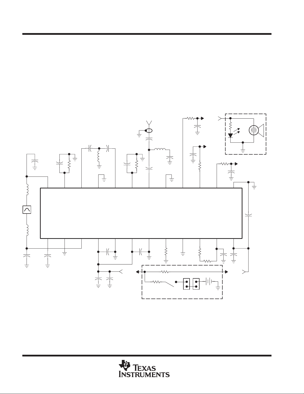
TRF1400 electrical characteristics are measured with the device connected in the circuit shown in Figure 1.
As with any RF design, the successful integration of the device into a circuit board relies heavily on the layout
of the board and the quality of the external components. Figures 2 through 6 show the layout of the circuit board
used to obtain the TRF1400 electrical characteristics. T able 1 lists the parts required to complete the test circuit,
which demonstrates TRF1400 performance at 315 MHz. Specified component tolerances (and Q where
applicable) should be observed during the selection of parts. Tables 2 through 4 give S parameters for each of
the RF signal processing blocks.
A complete set of Gerber photoplotter files for the circuit board can be obtained from any TI Field Sales Office.
L2
SAW
Filter
L3
C6
C2
R8
C20
C19
DOUT
AGND
DOUT
TRIG
R7
TRIG
OSCR
R4
R5
R11
LED
R6
C18
131415161718192021222324
BBOUT
OSCC
C15
RF Input
C9
C5
C7
RFOUT2
LPF
123456789101112
LNA2T
AGND
C10
RFIN2
RFIN3
C8
L4
C4
AGND
AVCC
RFOUT1
TRF1400 (U1)
AGND
C11 C12
AVCC
R1R2
LNA1T
C1
L1
C3
RFIN1
AGND
AGND
OFFSET
R3
Buzzer
BBOUT
DGND
DVCC
C16
+
Optional
C17
C13
C14
AVCC
R10
(Short)
R9
Optional
S1
E1 E2
H1 H2
(Jumpers)
Vcc1
B1X
DVCC
Figure 1. TRF1400 Test Circuit for 315-MHz Operation
6
POST OFFICE BOX 655303 • DALLAS, TEXAS 75265

TRF1400
RF TELEMETRY RECEIVERS
VHF/UHF RZ ASK REMOTE CONTROL RECEIVER
SLWS014E – JUNE 1996 – REVISED APRIL 1998
PARAMETER MEASUREMENT INFORMATION
NOTE A: Circuit board material is 62 mil G–10 with 1-oz copper, dielectric constant= 4.5
Figure 2. TRF1400 Test Circuit Board Layout — Top Side
Figure 3. TRF1400 Test Circuit Board Layout — Bottom Side
Figure 4. TRF1400 Test Circuit Board Solder Mask — Top Side
POST OFFICE BOX 655303 • DALLAS, TEXAS 75265
7

TRF1400
RF TELEMETRY RECEIVERS
VHF/UHF RZ ASK REMOTE CONTROL RECEIVER
SLWS014E – JUNE 1996 – REVISED APRIL 1998
PARAMETER MEASUREMENT INFORMATION
Figure 5. TRF1400 Test Circuit Board Solder Mask — Bottom Side
Figure 6. TRF1400 Test Circuit Board Silk Screen
8
POST OFFICE BOX 655303 • DALLAS, TEXAS 75265

Á
Á
Á
Á
Á
TRF1400
RF TELEMETRY RECEIVERS
VHF/UHF RZ ASK REMOTE CONTROL RECEIVER
SLWS014E – JUNE 1996 – REVISED APRIL 1998
PARAMETER MEASUREMENT INFORMATION
Table 1. TRF1400 315-MHz Test Circuit Parts List
DESIGNATORS
C1
C2, C3
C4, C7
C5
C6
C8
C9
C10
C11, C12, C17,
ÁÁÁÁ
C19
C13, C18, C20
C14, C16
C15
E1
E2
E3
H1, H2
F1
L1
L2
L3
L4
P1
R1
R2
R3
R4
R5
R6, R8
R7
R9
R10
R11
S1
Vcc1
B1X
U1
†
Tantalum capacitors are rated at 6.3 Vdc minimum.
DESCRIPTION
Capacitor
Capacitor
Capacitor
Capacitor
Capacitor
Capacitor
Capacitor
Capacitor
Capacitor
БББББ
Capacitor
Capacitor, Tantalum
Capacitor
2-Pin Connector
2-Pin Connector
6-Pin Connector
Header Shunts
SAW Filter
Inductor
Inductor
Inductor
Inductor
RF SMA Connector
Resistor
Resistor
Resistor
Resistor
Resistor
Resistor
Resistor
Resistor
Resistor
Resistor
Switch
Batttery Clip
Battery, Lithium
Receiver IC
†
VALUE
4 pF
22 pF
100 pF
5 pF
1.5 pF
3 pF
18 pF
0.047 µF
2200 pF
ББББББ
0.022 µF
4.7 µF @ 6.3 V
220 pF, 5%
RFM 1211
47 nH
82 nH
120 nH
39 nH
1.2 KΩ
1.2 KΩ
3 MΩ
130 KΩ, 1%
0 Ω
1K Ω
100 Ω
680 Ω
short
330 Ω
3.3-V Coin Cell (2 ea.)
TRF1400
MANUFACTURER
Murata
Murata
Murata
Murata
Murata
Murata
Murata
Murata
Murata
ÁÁÁÁ
Murata
Panasonic
Murata
3M
3M
3M
3M
RFM
Coilcraft
Coilcraft
Coilcraft
Coilcraft
Johnson
NKK
Keystone
Panasonic
TI
MANUFACTURER P/N
GRM40C0G040C050V
GRM40C0G220J050BD
GRM40C0G101J050BD
GRM40C0G050D050BD
GRM40C0G1R5C050BD
GRM40C0G030C050BD
GRM40C0G180J050BD
GRM40X7R473K050
GRM40X7R222K050BD
ББББББ
GRM40X7R223K050BL
ECS–T1AY475R
GRM40C0G221J050BD
2340–61 11–TN
2340–61 11–TN
2340–61 11–TN
929952–10
RFM 1211
0805HS470TMBC
0805HS820TKBC
0805HS121TKBC
0805HS390TMBC
142–0701–201
G-12AP
1061
CR2016
TRF1400
POST OFFICE BOX 655303 • DALLAS, TEXAS 75265
9

TRF1400
RF TELEMETRY RECEIVERS
VHF/UHF RZ ASK REMOTE CONTROL RECEIVER
SLWS014E – JUNE 1996 – REVISED APRIL 1998
PARAMETER MEASUREMENT INFORMATION
90%
RFIN1
10%
t
r
Rise Time
Figure 7. RFIN1 Rise and Fall Times
Fall Time
t
f
Table 2. TRF1400 LNA1 S Parameters
FREQ
(MHz)
300
304
310
315
318
390
418
434
NOTE 4: Input at RFIN1, output at RFOUT1, ZO=50 Ω, R
|S11|
0.9541
0.9555
0.9569
0.9474
0.9543
0.9391
0.9341
0.9270
∠ S11
–25.6217
–25.8350
–26.7244
–26.9720
–27.3058
–32.3782
–34.8677
–35.8675
|S21|
4.7618
4.7299
4.6670
4.6271
4.6075
3.8948
3.6575
3.5286
∠ S21
105.1213
103.9028
102.3880
100.8973
99.8886
81.7216
75.8867
72.4715
bias
|S12|
0.0042
0.0041
0.0033
0.0024
0.0028
0.0044
0.0019
0.0043
=1.2 kΩ
∠ S12
135.6601
82.5760
74.4905
108.9183
95.0878
–108.3656
165.4227
113.6352
|S22|
0.6699
0.6722
0.6670
0.6760
0.6724
0.691 1
0.6965
0.6991
∠ S22
–17.8126
–17.5588
–18.0246
–17.9033
–17.9506
–20.9576
–22.0900
–22.8623
10
POST OFFICE BOX 655303 • DALLAS, TEXAS 75265

ÁÁÁ
Á
Á
Á
Á
Á
Á
Á
Á
Á
ÁÁÁ
ÁÁÁ
ÁÁÁ
ÁÁÁ
ÁÁÁ
ÁÁÁ
ÁÁÁ
TRF1400
RF TELEMETRY RECEIVERS
VHF/UHF RZ ASK REMOTE CONTROL RECEIVER
SLWS014E – JUNE 1996 – REVISED APRIL 1998
PARAMETER MEASUREMENT INFORMATION
T able 3. TRF1400 LNA2 S Parameters
FREQ
ÁÁ
(MHz)
300
304
310
315
318
390
418
434
|S11|
ÁÁ
0.9607
0.9655
0.9554
0.9612
0.9615
0.9461
0.9389
0.9406
∠ S11
ÁÁ
–26.6188
–27.1490
–27.4384
–27.8929
–28.4482
–33.8905
–35.8847
–36.8175
|S21|
ÁÁ
4.8712
4.8380
4.7870
4.7239
4.7065
3.9755
3.741 1
3.6130
∠ S21
ÁÁ
100.9061
99.8060
97.8264
96.5227
95.5964
76.2949
69.8410
66.0262
NOTE 5: Input at RFIN2, output at RFOUT2, ZO=50 Ω, R
T able 4. TRF1400 RSSI S Parameters
FREQ.
(MHz)
300 0.7937 –23.6001
304 0.7895 –24.0484
310 0.7923 –24.4377
315 0.7931 –24.5069
318 0.7934 –24.8835
390 0.7851 –30.0440
418 0.7736 –31.2657
434 0.7805 –32.5896
NOTE 6: Input at RFIN3, ZO=50 Ω
|S11| ∠ S11
bias
|S12|
ÁÁ
0.0078
0.0057
0.0030
0.0014
0.0047
0.0054
0.0041
0.0046
=1.2 kΩ
∠ S12
ÁÁÁ
122.6680
65.9066
137.0205
31.2221
109.2950
48.3449
–119.9136
102.9654
|S22|
Á
0.6534
0.6555
0.6567
0.6572
0.6571
0.6803
0.681 1
0.6839
∠ S22
ÁÁÁ
–24.4258
–24.5020
–25.1 169
–24.8942
–25.0606
–28.0870
–29.5353
–30.4657
POST OFFICE BOX 655303 • DALLAS, TEXAS 75265
11

TRF1400
RF TELEMETRY RECEIVERS
VHF/UHF RZ ASK REMOTE CONTROL RECEIVER
SLWS014E – JUNE 1996 – REVISED APRIL 1998
PARAMETER MEASUREMENT INFORMATION
Manchester data format and timing
The TRF1400 requires specific Manchester data formatting and timing to decode and output Manchester serial
data. For the TRF1400 to output meaningful function data at the TRIG and DOUT terminals, the incoming RF
signal must have the Manchester-encoded binary format and timing shown in Figure 8 (for 50-kHz SCLK). A
wakeup time and frame-start time is required for the device to synchronize with the incoming data. The wakeup
time is designated by a data-bit 0 and data-bit 1 sequence repeated five times.
Figure 9 shows Manchester-encoded function data timing.
Function Data Starts
12345
(see Figure 9)
Input
100 µs
RF
0101010101Data
RF
Input
BBOUT
t
w3
DOUT
TRIG
010101 0101
t
x
(0.76 ms –
200 µs DOUT, TRIG Active During This Time
Wakeup Time = 200 µs 10 = 2 ms
(BBOUT Active During This Time)
SCLK = 50 kHz
6.34 ms)
Frame Start Time
(1.16 ms – 6.74ms)
Figure 8. Manchester-Encoded RF Binary Data Format at RF Input
Data 0 Data 1 Data 0 Data 1
t
d1
t
w1
t
w0
t
d2
Data 1
V
OH
V
OL
V
OH
V
OL
V
OH
V
OL
12
t
w2
Figure 9. Manchester-Encoded Function Data Timing Diagram
POST OFFICE BOX 655303 • DALLAS, TEXAS 75265

RF TELEMETRY RECEIVERS
VHF/UHF RZ ASK REMOTE CONTROL RECEIVER
SLWS014E – JUNE 1996 – REVISED APRIL 1998
PRINCIPLES OF OPERATION
general
The TRF1400 VHF/UHF RZ ASK remote control receiver demodulates AM RZ ASK modulated RF carriers
between 200 MHz and 450 MHz with a 500-Hz to 10-kHz baseband data rate or a 250-Hz to 5-kHz Manchester
data rate. A general signal flow is shown in Figure 10.
TRF1400
RF Input
RFOUT1 RFOUT2RFIN2
LC
RFIN1
LNA1
LC Filter
LNA2
RFIN3
Six Log-Detecting
RF Amp Stages
Auto Level/
Comparator
TRF1400
BBOUT
Manchester
Decoding
Logic
Figure 10. TRF1400 Signal Flow
signal reception
The RF signal is collected by an antenna and then passed through an external LC matching network to
bandpass filter the signal and compensate for various antenna loading impedances. The signal is then input
to the RFIN1 terminal of the TRF1400.
signal path through device
The RF signal applied to the RFIN1 terminal is amplified by LNA1 and typically passed through an external LC
matching network before being applied to the input of LNA2. The combined gain of the two LNAs is 40 dB, with
an input 1-dB compression point of –80 dBm and a noise figure of 5 dB (nominal). The amplified signal is output
at RFOUT2 and passed through an external preselector bandpass filter before being applied to the third stage
of amplification at terminal RFIN3.
The third stage of amplification consists of an amplifier with a single-ended input and differential outputs
followed by six high-gain differential log-detecting amplifier stages with an equivalent gain of 60 dB (nominal),
which forms a detector circuit. First, the signal is converted to a differential signal for increased noise immunity .
Next, the differential signal is passed through the six high-gain differential log-detecting amplifiers. Each
log-detecting amplifier is biased such that when an RF signal is present, an imbalance is caused in its bias
circuit. The imbalance in each of the six stages is converted to a voltage that is then summed into a baseband
envelope representation of the RF signal. This signal then passes through an autoleveling circuit before being
applied to a comparator to produce the TTL-level baseband signal output that appears at BBOUT. An external
low-pass filter connected to BBOUT attenuates high-frequency transients in the output signal.
DOUT
TRIG
The demodulated signal is also applied to the Manchester decoding and timing recovery logic section of the
TRF1400. The Manchester Decoding Logic section has two outputs, TRIG and DOUT, which should be
externally low-pass filtered to attenuate high-frequency transients. The signals appearing at these outputs are
meaningful only when the received Manchester-encoded data is formatted and timed as shown in Figure 9.
When Manchester-encoded data is received and demodulated, Manchester serial data is output at DOUT and
a trigger pulse is output at TRIG. The TRIG pulse rises at the start of each decoded data bit appearing at DOUT .
POST OFFICE BOX 655303 • DALLAS, TEXAS 75265
13

TRF1400
RF TELEMETRY RECEIVERS
VHF/UHF RZ ASK REMOTE CONTROL RECEIVER
SLWS014E – JUNE 1996 – REVISED APRIL 1998
PRINCIPLES OF OPERATION
frequency adjustment
The TRF1400 requires no manual alignment. The receive frequency is dependent only on the choice of external
matching networks and preselecting filters used. In that respect, the user has only to stock a different set of
external components for each frequency, and no manual alignment or end-of-line frequency programming is
required. Although the combination of the TRF1400 and test circuit/demo board (Figures 1 – 6) is optimized for
frequencies below 360 MHz, operation at reduced performance levels is possible at higher frequencies.
external components and device performance
Whereas the TRF1400 uses a minimum of external components in the typical application, the choice of those
components greatly affects the performance of the device. When a SAW (surface acoustic wave) preselector
is used, the selectivity (out-of-band rejection) and sensitivity of the TRF1400 are optimized as a result of the
high Q of SAW devices. If an LC preselector is used, these parameters change and the overall performance
of the TRF1400 is reduced, but can still meet the requirements of many end-equipment applications.
An external resistor connected between OFFSET and ground adjusts the internal offset voltage of the receiver
decoding section to maximize the noise rejection of the device. While a 3-MΩ resistor is suggested, this value
can be changed to minimize toggling of outputs DOUT , TRIG, and BBOUT during periods of nonvalid received
code.
decoder interface
For baseband operation, a decoder can be interfaced directly to the TRF1400 using the baseband-data output
(BBOUT) of the device.
For Manchester operation, a standard microcontroller decoder must know when to poll its input for data. The
TRF1400 provides an output terminal (TRIG) for this purpose that pulses on each valid received data cell. In
this system configuration, Manchester-encoded binary data must be used in the format described in the
following paragraphs to allow the TRF1400 to synchronize properly and produce the TRIG and DOUT outputs.
internal clock/synchronization
An internal clock (SCLK) is used by the TRF1400 for processing the demodulated incoming data stream and
for controlling the Manchester-decoding and timing-recovery logic sections of the device. The frequency of
SCLK is set by an external resistor connected between the OSCR and OSCC terminals and an external
capacitor connected between OSCC and ground, and is adjustable between 2.5 kHz and 50 kHz.
For baseband output, SCLK is set to 5 times the received baseband data rate (500 Hz to 10 kHz). Incoming
baseband data is then sampled at 5 times its transmitted data rate. TTL-level baseband data is output at BBOUT
whenever the TRF1400 receives ASK-modulated data in any format. This provides compatibility with systems
that use other code formatting, and whose serial data decoders do not require the DOUT or TRIG outputs from
the receiver.
For Manchester data output, SCLK must be set to 10 times the received Manchester-encoded data rate (250 Hz
to 5 kHz) for the output signals at TRIG and DOUT to be meaningful. The high sampling rate (10×) ensures
accurate correlation of the received signal.
The received Manchester data rate (set by a clock on the transmitter/encoder end) can vary as much as ±8%
and TRF1400 synchronization still results. This allows for frequency drift due to external component tolerances
and temperature changes on the transmitter end. At the TRF1400 end, a ± 8% frequency variation is also
allowed. Thus, the total permissible frequency variation from transmitter clock to receiver clock can be as much
as ±16%. For example, if a serial Manchester data rate of 1.5 kHz is used at the encoder/transmitter end, then
the TRF1400 sample clock oscillator (SCLK) must be set to 10 times the transmitted data rate, or 15 kHz. SCLK
is allowed to vary ±8% in frequency, from 13.8 kHz to 16.2 kHz in this case, and the TRF1400 synchronizes
successfully to the incoming data.
14
POST OFFICE BOX 655303 • DALLAS, TEXAS 75265

RF TELEMETRY RECEIVERS
VHF/UHF RZ ASK REMOTE CONTROL RECEIVER
SLWS014E – JUNE 1996 – REVISED APRIL 1998
PRINCIPLES OF OPERATION
internal clock/synchronization (continued)
The data rate of the incoming data itself can also vary the same amount. It is left to the user to design the system
such that the transmitter/encoder data rate drifts ±8% or less. The TRF1400 can introduce as much as a ±5%
frequency variation due to its internal tolerances and semiconductor process variations, so the external resistor
and capacitor values used with the TRF1400 can have up to a ±3% value tolerance.
The frequency of the internal clock oscillator is set by connecting a resistor between OSCR and OSCC and a
capacitor between OSCC and ground. The following equation defines the oscillator frequency (SCLK speed)
as a function of the external resistor and capacitor:
TRF1400
ext
)
1
R
Ǔ ǒ
s
)
Ǔ
C
p
C
ext
F
+
osc
Where: R
1.386
ext
R
s
C
ext
C
p
ǒ
R
is the external resistor connected between OSCR and OSCC.
is the internal series resistance, typically 1.9 kΩ or less.
is the external capacitor connected between OSCC and ground.
is parasitic capacitance and is dependent on board layout — typical value is 8.5 pF.
For minimum current draw, large values (in the thousands of ohms) for R
and the resulting SCLK frequency when C
100
80
60
40
f – SCLK Frequency – kHz
20
= 100 pF are shown in Figure 11.
ext
should be used. Typical R
ext
C
= 100 pF
ext
ext
values
0
0 200 k 400 k 600 k
R – Resistance – Ω
800 k 1 M
1.2 M 1.4 M
Figure 11. External Resistance Versus Sample Clock Frequency
POST OFFICE BOX 655303 • DALLAS, TEXAS 75265
15

TRF1400
RF TELEMETRY RECEIVERS
VHF/UHF RZ ASK REMOTE CONTROL RECEIVER
SLWS014E – JUNE 1996 – REVISED APRIL 1998
APPLICABLE REGULATIONS
Receiver design, as well as transmitter design, is regulated throughout the world. Since the TRF1400 is targeted for
world-wide sales, the applicable standard for each region must be considered when the device is to be used in
systems to be successfully marketed in that region. For this reason, the TRF1400 conforms to all requirements shown
in Figure 12 and T able 5. The primary specifications of most of the standards address carrier frequency and spurious
emissions.
CANADA
Dept. of Communications (DoC),
Telecom Regulatory Service,
USA
Federal Communications
Commission (FCC) Code of
Federal Regulations 47
(CFR 47) Parts 15.35, 15.205,
15.209, and 15.231, 260–470 MHz,
and Part 15.249, 902–928 MHz
(see Table 5)
Radio Standard Specifications
(RSS), RSS-210, 260–470 MHz
and 902–928 MHz
SOUTH AFRICA
403.916 MHz and
411.6 MHz
ISRAEL
Ministry of
Communications,
Engineering, and
Licensing Div ., 325 MHz
AUSTRALIA
Dept. of Transportation and
Telecommunications (DTC),
and ECR60, 303.825 MHz
and 318 MHz
JAPAN
Ministry of Posts &
Telecommunications
(MPT) < 322 MHz
HONG KONG
Post Office, Telecom
Branch, Telecom
Order 1989, Sec 39,
Chap. 106, 314 MHz
GERMANY
Femmeldetechnisches
Zentralamt (FTZ), FTZ
17 TR 2100, 433.92 MHz
UNITED KINGDOM
Dept. of Trade and Industry
(DTI), MPT 1340, 418 MHz,
and for automotive only:
433.92 MHz
FRANCE
Centre National d′Etudes des
T′el′ecommunications
(National Telecom Research Center , CNET),
Groupement Terminaux Procedures et
Applications (Terminals, Procedures, and
Applications Group, TPA), Specification
Technique (ST), ST/PAA/TPA/AGH/1542,
223.5–225 MHz and for automotive only:
433.92 MHz
Figure 12. World-Wide Receiver Regulations
The Interim European
Telecommunications Standard, I-ETS 300
220 (433.92 MHz) is proposed by the
European Telecommunications
Standards Institute (ETSI) for all
European Community (EC) countries.
Most European countries not shown
currently use 433.92 MHz according to
CEPT recommendations and are likely to
adopt rules similar to ETSI I-ETS 300 220.
16
POST OFFICE BOX 655303 • DALLAS, TEXAS 75265

TRF1400
RF TELEMETRY RECEIVERS
VHF/UHF RZ ASK REMOTE CONTROL RECEIVER
SLWS014E – JUNE 1996 – REVISED APRIL 1998
APPLICABLE REGULATIONS
Table 5. World-Wide Regulations
REGION REGULATION FREQUENCY
USA Federal Communications Commission (FCC) Code of
Federal Regulations 47 (CFR 47) Parts 15.35, 15.205,
15.209, 15.231, and 15.249 (see Note 7)
Germany Femmeldetechnisches Zentralamt (FTZ), FTZ 17 TR2100 433.92 MHz
France Centre National d′Etudes des T′el′ecommunications
(National Telecom Research Center, CNET), Groupement
Terminaux Procedures et Applications (Terminals,
Procedures and Applications Group, TPA), Specification
Technique (ST), ST/P AA/TPA/AGH/1542
United Kingdom Dept. of Trade and Industry (DTI), MPT 1340 418 MHz
Japan Ministry of Posts and Telecommunications (MPT) < 322 MHz
Canada Dept. of Communications (DoC), Telecom Regulatory
Service, Radio Standard Specifications (RSS), RSS-210
Hong Kong Post Office, Telecom Branch, Telecom Order 1989,
Sec 39, Cap. 106
Australia Dept. of Transportation and Telecommunications (DTC),
and ECR60
Israel Ministry of Communications, Engineering & Licensing Div. 325 MHz
South Africa 403.916 MHz and 41 1.6 MHz
NOTE 7: Although the FCC Part 15.231 allows low-power unlicensed radios in the range of 260 MHz to 470 MHz, not all frequencies in this range
are desirable. This is due to emission restrictions applying to fundamentals and harmonics in various forbidden bands as defined in Parts
15.205 and 15.209. USA frequencies shown above conform to these additional restrictions and are commonly used in the USA. Under
Part 15.249, transmitters may continuously radiate 50 000 µV/m at 3 meters with simple modulation. Part 15.247 permits still higher
power, but must use true spread-spectrum modulation. See FCC CFR 47, Part 47, Part 15 for details.
260 MHz – 470 MHz (Part 15.35, 15.205, 15.209)
902 MHz – 928 MHz (Part 15.249, see Note 4)
223.5 MHz – 225 MHz (automotive only)
433.92 MHz (automotive only)
260 MHz – 470 MHz (RSS-210)
902 MHz – 928 MHz
314 MHz
303.825 MHz and 318 MHz
POST OFFICE BOX 655303 • DALLAS, TEXAS 75265
17

TRF1400
RF TELEMETRY RECEIVERS
VHF/UHF RZ ASK REMOTE CONTROL RECEIVER
SLWS014E – JUNE 1996 – REVISED APRIL 1998
MECHANICAL DATA
DW (R-PDSO-G**) PLASTIC SMALL-OUTLINE PACKAGE
16 PIN SHOWN
0.050 (1,27)
16
1
0.020 (0,51)
0.014 (0,35)
9
0.299 (7,59)
0.293 (7,45)
8
A
0.010 (0,25)
0.419 (10,65)
0.400 (10,15)
M
0.010 (0,25) NOM
0°–8°
Gage Plane
0.010 (0,25)
0.050 (1,27)
0.016 (0,40)
0.104 (2,65) MAX
NOTES: A. All linear dimensions are in inches (millimeters).
B. This drawing is subject to change without notice.
C. Body dimensions do not include mold flash or protrusion not to exceed 0.006 (0,15).
D. Falls within JEDEC MS-013
0.012 (0,30)
0.004 (0,10)
PINS **
DIM
A MAX
A MIN
Seating Plane
0.004 (0,10)
16
0.410
(10,41)
0.400
(10,16)
0.510
(12,95)
0.500
(12,70)
20
24
0.610
(15,49)
0.600
(15,24)
4040000/D 02/98
18
POST OFFICE BOX 655303 • DALLAS, TEXAS 75265

IMPORTANT NOTICE
T exas Instruments and its subsidiaries (TI) reserve the right to make changes to their products or to discontinue
any product or service without notice, and advise customers to obtain the latest version of relevant information
to verify, before placing orders, that information being relied on is current and complete. All products are sold
subject to the terms and conditions of sale supplied at the time of order acknowledgement, including those
pertaining to warranty, patent infringement, and limitation of liability.
TI warrants performance of its semiconductor products to the specifications applicable at the time of sale in
accordance with TI’s standard warranty. Testing and other quality control techniques are utilized to the extent
TI deems necessary to support this warranty . Specific testing of all parameters of each device is not necessarily
performed, except those mandated by government requirements.
CERT AIN APPLICATIONS USING SEMICONDUCTOR PRODUCTS MAY INVOLVE POTENTIAL RISKS OF
DEATH, PERSONAL INJURY, OR SEVERE PROPERTY OR ENVIRONMENTAL DAMAGE (“CRITICAL
APPLICATIONS”). TI SEMICONDUCTOR PRODUCTS ARE NOT DESIGNED, AUTHORIZED, OR
WARRANTED TO BE SUITABLE FOR USE IN LIFE-SUPPORT DEVICES OR SYSTEMS OR OTHER
CRITICAL APPLICA TIONS. INCLUSION OF TI PRODUCTS IN SUCH APPLICATIONS IS UNDERST OOD TO
BE FULLY AT THE CUSTOMER’S RISK.
In order to minimize risks associated with the customer’s applications, adequate design and operating
safeguards must be provided by the customer to minimize inherent or procedural hazards.
TI assumes no liability for applications assistance or customer product design. TI does not warrant or represent
that any license, either express or implied, is granted under any patent right, copyright, mask work right, or other
intellectual property right of TI covering or relating to any combination, machine, or process in which such
semiconductor products or services might be or are used. TI’s publication of information regarding any third
party’s products or services does not constitute TI’s approval, warranty or endorsement thereof.
Copyright 1998, Texas Instruments Incorporated
 Loading...