

Texas Instruments TPS76633DR, TPS76633D, TPS76630PWR, TPS76630D, TPS76630DR Datasheet
...
TPS76615, TPS76618, TPS76625, TPS76627
TPS76628, TPS76630, TPS76633, TPS76650, TPS76601
ULTRA LOW QUIESCENT CURRENT 250-mA LOW-DROPOUT VOLTAGE REGULATORS
SLVS237 – AUGUST 1999
1
POST OFFICE BOX 655303 • DALLAS, TEXAS 75265
D
250-mA Low-Dropout Voltage Regulator
D
Available in 1.5-V, 1.8-V, 2.5-V, 2.7-V, 2.8-V,
3.0-V, 3.3-V, 5.0-V Fixed Output and
Adjustable Versions
D
Dropout Voltage to 140 mV (Typ) at 250 mA
(TPS76650)
D
Ultra-Low 35-µA Typical Quiescent Current
D
3% Tolerance Over Specified Conditions for
Fixed-Output Versions
D
Open Drain Power Good
D
8-Pin SOIC Package
D
Thermal Shutdown Protection
description
This device is designed to have an ultra-low quiescent current and be stable with a 4.7-µF capacitor. This
combination provides high performance at a reasonable cost.
Because the PMOS device behaves as a low-value resistor, the dropout voltage is very low (typically 230 mV
at an output current of 250 mA for the TPS76650) and is directly proportional to the output current. Additionally ,
since the PMOS pass element is a voltage-driven device, the quiescent current is very low and independent
of output loading (typically 35 µA over the full range of output current, 0 mA to 250 mA). These two key
specifications yield a significant improvement in operating life for battery-powered systems. This LDO family
also features a sleep mode; applying a TTL high signal to EN
(enable) shuts down the regulator, reducing the
quiescent current to less than 1 µA (typ).
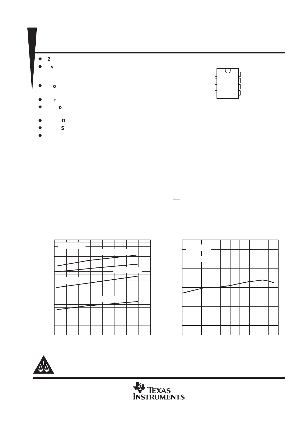
TA – Free-Air Temperature – °C
– Output Voltage – V
V
DO
TPS76633
DROPOUT VOLTAGE
vs
FREE-AIR TEMPERATURE
–50 –25 0 25 50 75 100 125 150
VI = 3.2 V
IO = 10 mA
IO = 50 mA
IO = 150 mA
10
0
10
–1
10
–2
10
–3
IO = 250 mA
34
34.1
34.2
34.3
34.4
34.5
34.6
34.7
34.8
34.9
35.0
0 25 50 75 100 125 150 175 200 225 250
IL – Load Current – mA
TPS76633
GROUND CURRENT
vs
LOAD CURRENT
VO = 3.3 V
GND
I – Ground Current – Aµ
TA = 25°C
Please be aware that an important notice concerning availability, standard warranty, and use in critical applications of
Texas Instruments semiconductor products and disclaimers thereto appears at the end of this data sheet.
PRODUCTION DATA information is current as of publication date.
Products conform to specifications per the terms of Texas Instruments
standard warranty. Production processing does not necessarily include
testing of all parameters.
Copyright 1999, Texas Instruments Incorporated
1
2
3
4
8
7
6
5
NC/FB
PG
GND
EN
OUT
OUT
IN
IN
D PACKAGE
(TOP VIEW)
TPS76615, TPS76618, TPS76625, TPS76627
TPS76628, TPS76630, TPS76633, TPS76650, TPS76601
ULTRA LOW QUIESCENT CURRENT 250-mA LOW-DROPOUT VOLTAGE REGULATORS
SLVS237 – AUGUST 1999
2
POST OFFICE BOX 655303 • DALLAS, TEXAS 75265
description (continued)
Power good (PG) is an active high output, which can be used to implement a power-on reset or a low-battery
indicator.
The TPS766xx is offered in 1.5-V, 1.8-V, 2.5-V, 2.7-V, 2.8-V, 3.0-V , 3.3-V and 5.0-V fixed-voltage versions and
in an adjustable version (programmable over the range of 1.25 V to 5.5 V). Output voltage tolerance is specified
as a maximum of 3% over line, load, and temperature ranges. The TPS766xx family is available in 8 pin SOIC
package.
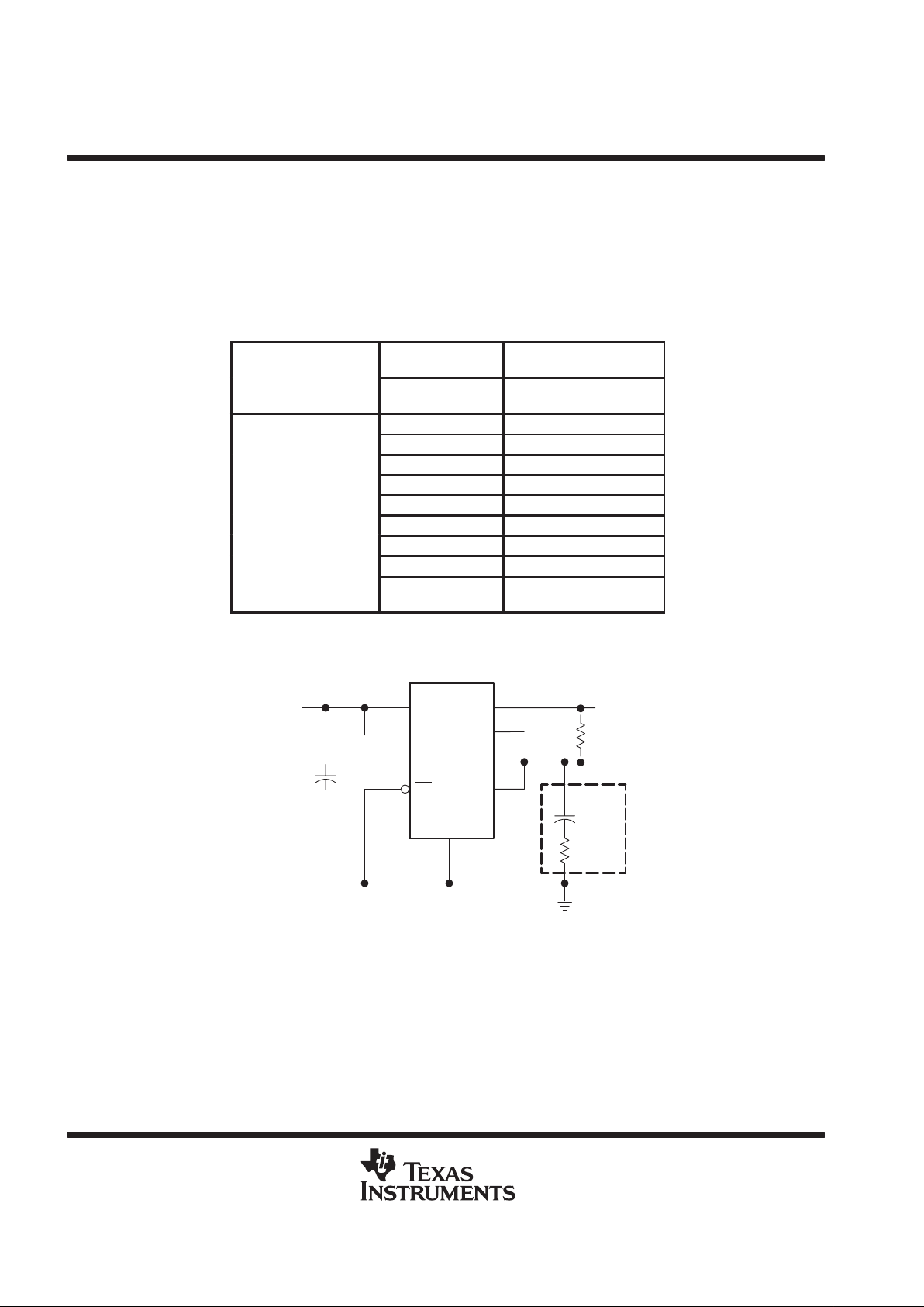
AVAILABLE OPTIONS
OUTPUT VOLTAGE
(V)
PACKAGED DEVICES
T
J
TYP
SOIC
(D)
5.0 TPS76650D
3.3 TPS76633D
3.0 TPS76630D
2.8 TPS76628D
–
°
°
2.7 TPS76627D
–40 C to 125 C
2.5 TPS76625D
1.8 TPS76618D
1.5 TPS76615D
Adjustable
1.25 V to 5.5 V
TPS76601D
The TPS76601 is programmable using an external resistor divider (see application
information). The D package is available taped and reeled. Add an R suffix to the
device type (e.g., TPS76601DR).
†
See application information section for capacitor selection details.
PG
OUT
OUT
6
5
4
IN
IN
EN
GND
3
2
7
8
V
I
0.1 µF
PG
V
O
4.7 µF
+
TPS766xx
C
O
†
1
NC/FB
300 mΩ
Figure 1. Typical Application Configuration for Fixed Output Options
TPS76615, TPS76618, TPS76625, TPS76627
TPS76628, TPS76630, TPS76633, TPS76650, TPS76601
ULTRA LOW QUIESCENT CURRENT 250-mA LOW-DROPOUT VOLTAGE REGULATORS
SLVS237 – AUGUST 1999
3
POST OFFICE BOX 655303 • DALLAS, TEXAS 75265
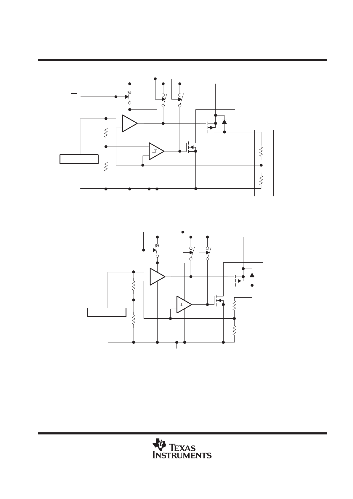
functional block diagram—adjustable version
_
+
V
ref
= 1.224 V
OUT
FB/NC
EN
GND
PG
_
+
IN
External to the device
R1
R2
functional block diagram—fixed-voltage version
_
+
V
ref
= 1.224 V
OUT
EN
GND
R1
R2
_
+
IN
PG
TPS76615, TPS76618, TPS76625, TPS76627
TPS76628, TPS76630, TPS76633, TPS76650, TPS76601
ULTRA LOW QUIESCENT CURRENT 250-mA LOW-DROPOUT VOLTAGE REGULATORS
SLVS237 – AUGUST 1999
4
POST OFFICE BOX 655303 • DALLAS, TEXAS 75265
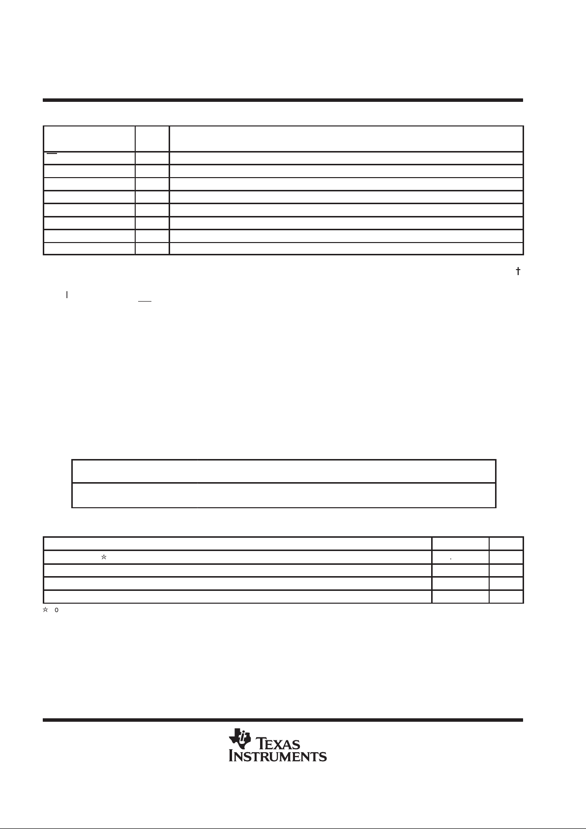
Terminal Functions – SOIC Package
TERMINAL
NAME NO.
I/O
DESCRIPTION
EN 4 I Enable input
FB/NC 1 I Feedback input voltage for adjustable device (no connect for fixed options)
GND 3 Regulator ground
IN 5 I Input voltage
IN 6 I Input voltage
OUT 7 O Regulated output voltage
OUT 8 O Regulated output voltage
PG 2 O PG output
absolute maximum ratings over operating free-air temperature range (unless otherwise noted)
Ĕ
Input voltage range‡, VI –0.3 V to 13.5 V. . . . . . . . . . . . . . . . . . . . . . . . . . . . . . . . . . . . . . . . . . . . . . . . . . . . . . . . . .
Voltage range at EN
–0.3 V to 16.5 V. . . . . . . . . . . . . . . . . . . . . . . . . . . . . . . . . . . . . . . . . . . . . . . . . . . . . . . . . . . . . .
Maximum PG voltage 16.5 V. . . . . . . . . . . . . . . . . . . . . . . . . . . . . . . . . . . . . . . . . . . . . . . . . . . . . . . . . . . . . . . . . . . . .
Peak output current Internally limited. . . . . . . . . . . . . . . . . . . . . . . . . . . . . . . . . . . . . . . . . . . . . . . . . . . . . . . . . . . . . .
Continuous total power dissipation See dissipation rating tables. . . . . . . . . . . . . . . . . . . . . . . . . . . . . . . . . . . . . .
Output voltage, VO (OUT, FB) 7 V. . . . . . . . . . . . . . . . . . . . . . . . . . . . . . . . . . . . . . . . . . . . . . . . . . . . . . . . . . . . . . . .
Operating virtual junction temperature range, T
J
–40°C to 125°C. . . . . . . . . . . . . . . . . . . . . . . . . . . . . . . . . . . . .
Storage temperature range, T
stg
–65°C to 150°C. . . . . . . . . . . . . . . . . . . . . . . . . . . . . . . . . . . . . . . . . . . . . . . . . . .
ESD rating, HBM 2 kV. . . . . . . . . . . . . . . . . . . . . . . . . . . . . . . . . . . . . . . . . . . . . . . . . . . . . . . . . . . . . . . . . . . . . . . . . .
†
Stresses beyond those listed under “absolute maximum ratings” may cause permanent damage to the device. These are stress ratings only, and
functional operation of the device at these or any other conditions beyond those indicated under “recommended operating conditions” is not
implied. Exposure to absolute-maximum-rated conditions for extended periods may affect device reliability.
‡
All voltage values are with respect to network terminal ground.
DISSIPATION RATING TABLE 1 – FREE-AIR TEMPERATURES
PACKAGE
AIR FLOW
(CFM)
TA < 25°C
POWER RATING
DERATING FACTOR
ABOVE TA = 25°C
TA = 70°C
POWER RATING
TA = 85°C
POWER RATING
0 568 mW 5.68 mW/°C 312 mW 227 mW
D
250 904 mW 9.04 mW/°C 497 mW 361 mW
recommended operating conditions
MIN MAX UNIT
Input voltage, V
I
k
2.7 10 V
Output voltage range, V
O
1.2 5.5 V
Output current, IO (Note 1) 0 250 mA
Operating virtual junction temperature, TJ (Note 1) –40 125 °C
k
To calculate the minimum input voltage for your maximum output current, use the following equation: V
I(min)
= V
O(max)
+ V
DO(max load)
.
NOTE 1: Continuous current and operating junction temperature are limited by internal protection circuitry, but it is not recommended that the
device operate under conditions beyond those specified in this table for extended periods of time.
TPS76615, TPS76618, TPS76625, TPS76627
TPS76628, TPS76630, TPS76633, TPS76650, TPS76601
ULTRA LOW QUIESCENT CURRENT 250-mA LOW-DROPOUT VOLTAGE REGULATORS
SLVS237 – AUGUST 1999
5
POST OFFICE BOX 655303 • DALLAS, TEXAS 75265
electrical characteristics over recommended operating free-air temperature range,
V
i
= V
O(typ)
+ 1 V, I
O
= 10 µA, EN = 0 V, CO = 4.7 µF (unless otherwise noted)
PARAMETER TEST CONDITIONS MIN TYP MAX UNIT
5.5 V ≥ VO ≥ 1.25 V, TJ = 25°C V
O
TPS76601
5.5 V ≥ VO ≥ 1.25 V, TJ = –40°C to 125°C 0.97V
O
1.03V
O
TJ = 25°C, 2.7 V < VIN < 10 V 1.5
TPS76615
TJ = –40°C to 125°C, 2.7 V < VIN < 10 V 1.455 1.545
TJ = 25°C, 2.8 V < VIN < 10 V 1.8
TPS76618
TJ = –40°C to 125°C, 2.8 V < VIN < 10 V 1.746 1.854
TJ = 25°C, 3.5 V < VIN < 10 V 2.5
TPS76625
TJ = –40°C to 125°C, 3.5 V < VIN < 10 V 2.425 2.575
Output voltage
TJ = 25°C, 3.7 V < VIN < 10 V 2.7
(10 µA to 250 mA load)
(see
Note 2
)
TPS76627
TJ = –40°C to 125°C, 3.7 V < VIN < 10 V 2.619 2.781
V
(see Note 2)
TJ = 25°C, 3.8 V < VIN < 10 V 2.8
TPS76628
TJ = –40°C to 125°C, 3.8 V < VIN < 10 V 2.716 2.884
TJ = 25°C, 4.0 V < VIN < 10 V 3.0
TPS76630
TJ = –40°C to 125°C, 4.0 V < VIN < 10 V 2.910 3.090
TJ = 25°C, 4.3 V < VIN < 10 V 3.3
TPS76633
TJ = –40°C to 125°C, 4.3 V < VIN < 10 V 3.201 3.399
TJ = 25°C, 6.0 V < VIN < 10 V 5.0
TPS76650
TJ = –40°C to 125°C, 6.0 V < VIN < 10 V 4.850 5.150
Quiescent current (GND current)
10 µA < IO < 250 mA, TJ = 25°C 35
()
EN = 0V, (see Note 2)
IO = 250 mA, TJ = –40°C to 125°C 50
µ
A
Output voltage line regulation (∆VO/V
O
)
(see Notes 2 and 3)
VO + 1 V < VI ≤ 10 V, TJ = 25°C 0.01 %/V
Load regulation IO = 10 µA to 250 mA 0.5%
Output noise voltage
BW = 300 Hz to 50 kHz,
CO = 4.7 µF, TJ = 25°C
200 µVrms
Output current Limit VO = 0 V 0.8 1.2 A
Thermal shutdown junction temperature 150 °C
EN = V
I,
TJ = 25°C,
2.7 V < VI < 10 V
1 µA
Standby current
EN = V
I,
TJ = –40°C to 125°C
2.7 V < VI < 10 V
10 µA
FB input current TPS76601 FB = 1.5 V 2 nA
High level enable input voltage 2.0 V
Low level enable input voltage 0.8 V
Power supply ripple rejection (see Note 2)
f = 1 kHz, CO = 4.7 µF,
IO = 10 µA, TJ = 25°C
63 dB
Minimum input voltage for valid PG I
O(PG)
= 300µA 1.1 V
Trip threshold voltage VO decreasing 92 98 %V
O
PG
Hysteresis voltage Measured at V
O
0.5 %V
O
Output low voltage VI = 2.7 V, I
O(PG)
= 1mA 0.15 0.4 V
Leakage current V
(PG)
= 5 V 1 µA
p
EN = 0 V –1 0 1
Input current (EN)
EN = V
I
–1 1
µ
A
NOTE: 2. Minimum IN operating voltage is 2.7 V or V
O(typ)
+ 1 V, whichever is greater. Maximum IN voltage 10 V.
TPS76615, TPS76618, TPS76625, TPS76627
TPS76628, TPS76630, TPS76633, TPS76650, TPS76601
ULTRA LOW QUIESCENT CURRENT 250-mA LOW-DROPOUT VOLTAGE REGULATORS
SLVS237 – AUGUST 1999
6
POST OFFICE BOX 655303 • DALLAS, TEXAS 75265
electrical characteristics over recommended operating free-air temperature range,
V
i
= V
O(typ)
+ 1 V, I
O
= 10 µA, EN = 0 V, CO = 4.7 µF (unless otherwise noted) (continued)
PARAMETER TEST CONDITIONS MIN TYP MAX UNIT
IO = 250 mA, TJ = 25°C 310
TPS76628
IO = 250 mA, TJ = –40°C to 125°C 540
IO = 250 mA, TJ = 25°C 270
Dropout voltage
TPS76630
IO = 250 mA, TJ = –40°C to 125°C 470
g
(See Note 4)
IO = 250 mA, TJ = 25°C 230
mV
TPS76633
IO = 250 mA, TJ = –40°C to 125°C 400
IO = 250 mA, TJ = 25°C 140
TPS76650
IO = 250 mA, TJ = –40°C to 125°C 250
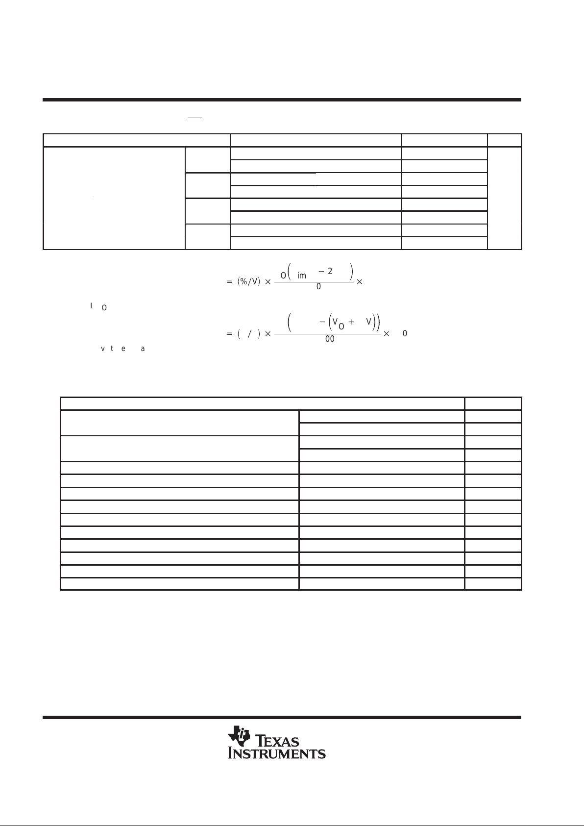
NOTES: 3. If VO ≤ 1.8 V then V
imin
= 2.7 V, V
imax
= 10 V:
Line Reg. (mV)
+ǒ%ńVǓ
V
O
ǒ
V
imax
*
2.7 V
Ǔ
100
1000
If VO ≥ 2.5 V then V
imin
= VO + 1 V, V
imax
= 10 V:
Line Reg. (mV)
+ǒ%ńVǓ
V
O
ǒ
V
imax
*ǒVO)
1V
Ǔ
Ǔ
100
1000
4. IN voltage equals VO(Typ) – 100 mV; TPS76601 output voltage set to 3.3 V nominal with external resistor divider. TPS76615,
TPS76618, TPS76625, and TPS76627 dropout voltage limited by input voltage range limitations (i.e., TPS76630 input voltage
needs to drop to 2.9 V for purpose of this test).
Table of Graphs
FIGURE
p
vs Load current 2, 3
Output voltage
vs Free-air temperature 4, 5
vs Load current 6, 7
Ground current
vs Free-air temperature 8, 9
Power supply ripple rejection vs Frequency 10
Output spectral noise density vs Frequency 11
Output impedance vs Frequency 12
Dropout voltage vs Free-air temperature 13, 14
Line transient response 15, 17
Load transient response 16, 18
Output voltage vs Time 19
Dropout voltage vs Input voltage 20
Equivalent series resistance (ESR) vs Output current 21 – 24
Equivalent series resistance (ESR) vs Added ceramic capacitance 25, 26
 Loading...