

Texas Instruments TPS75433QPWPR, TPS75433QPWP, TPS75425QPWPR, TPS75425QPWP, TPS75418QPWP Datasheet
...
TPS75201Q, TPS75215Q, TPS75218Q, TPS75225Q, TPS75233Q WITH RESET
TPS75401Q, TPS75415Q, TPS75418Q, TPS75425Q, TPS75433Q WITH POWER GOOD
FAST-TRANSIENT-RESPONSE 2-A LOW-DROPOUT VOLTAGE REGULATORS
SLVS242 – MARCH 2000
D
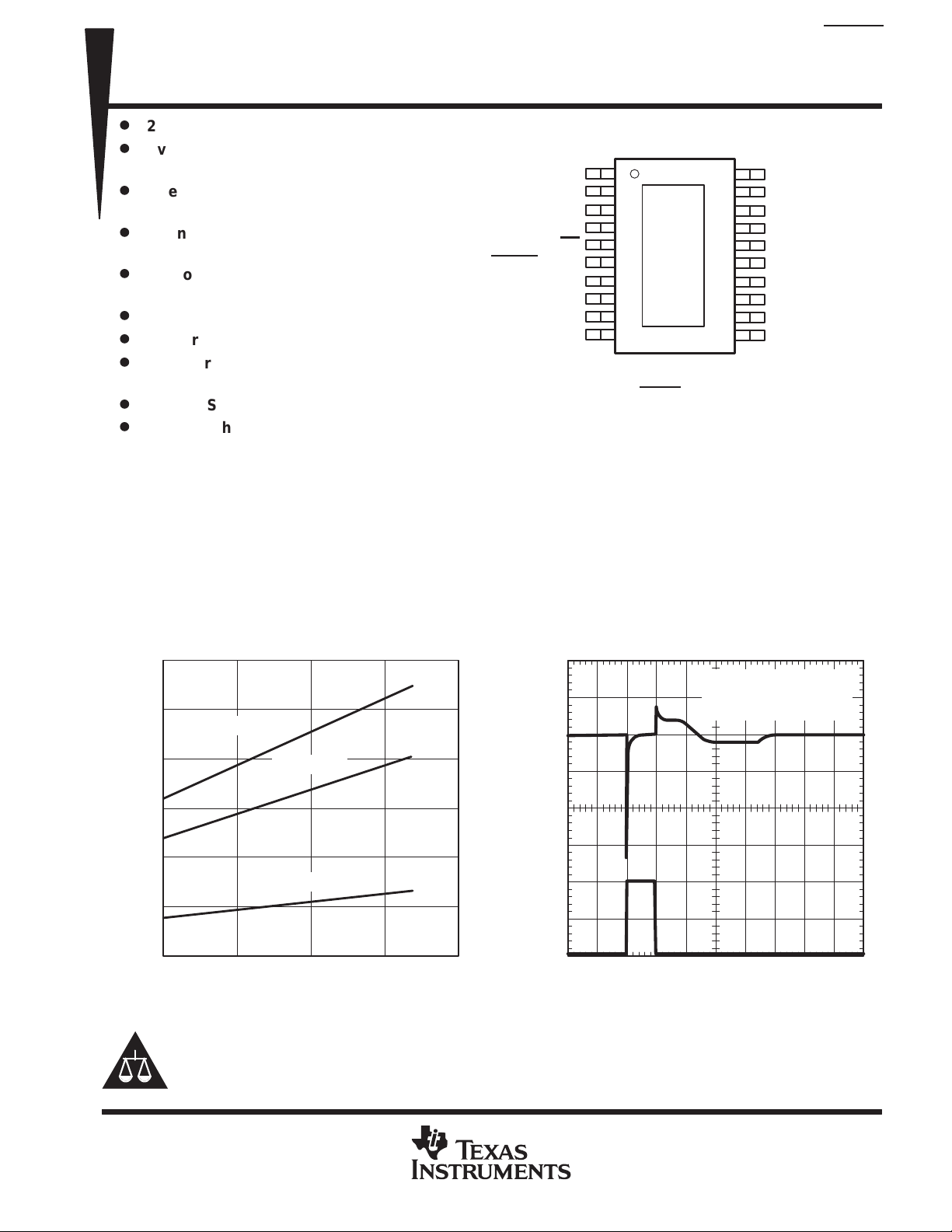
2-A Low-Dropout Voltage Regulator
D
Available in 1.5-V, 1.8-V, 2.5-V , 3.3-V Fixed
Output and Adjustable Versions
D
Open Drain Power-On Reset With 100-ms
Delay (TPS752xxQ)
D
Open Drain Power-Good (PG) Status
Output (TPS754xxQ)
D
Dropout Voltage Typically 210 mV at 2 A
(TPS75233Q)
D
Ultra Low 75-µA Typical Quiescent Current
D
Fast Transient Response
D
2% Tolerance Over Specified Conditions
for Fixed-Output Versions
D
20-Pin TSSOP (PWP) PowerP AD Package
D
Thermal Shutdown Protection
GND/HEATSINK
NC
IN
IN
EN
RESETor PG
†
FB/SENSE
OUTPUT
OUTPUT
GND/HEATSINK
NC – No internal connection
†
PG is on the TPS754xx and RESET
PWP PACKAGE
(TOP VIEW)
1
2
3
4
5
6
7
8
9
10
is on the TPS752xx
20
19
18
17
16
15
14
13
12
11
GND/HEATSINK
NC
NC
GND
NC
NC
NC
NC
NC
GND/HEATSINK
description
The TPS752xxQ and TPS754xxQ are low dropout regulators with integrated power-on reset and power good
(PG) functions respectively . These devices are capable of supplying 2 A of output current with a dropout of 210
mV (TPS75233Q, TPS75433Q). Quiescent current is 75 µA at full load and drops down to 1 µA when the device
is disabled. TPS752xxQ and TPS754xxQ are designed to have fast transient response for larger load current
changes.
TPS75x33Q
300
250
200
150
DROPOUT VOLTAGE
vs
JUNCTION TEMPERATURE
IO = 2 A
IO = 1.5 A
50
0
– Change in∆
O
V
–50
Output Voltage – mV
–100
LOAD TRANSIENT RESPONSE
TPS75x33Q
IL=2 A
CL=100 µF (T antalum)
VO=3.3 V
100
– Dropout Voltage – mV
DO
V
50
0
–40 10 11060
Please be aware that an important notice concerning availability, standard warranty, and use in critical applications of
Texas Instruments semiconductor products and disclaimers thereto appears at the end of this data sheet.
PowerPAD is a trademark of Texas Instruments.
PRODUCTION DATA information is current as of publication date.
Products conform to specifications per the terms of Texas Instruments
standard warranty. Production processing does not necessarily include
testing of all parameters.
IO = 0.5 A
TJ – Junction Temperature – °C
–150
2
1
O
I – Output Current – A
160
POST OFFICE BOX 655303 • DALLAS, TEXAS 75265
0
321457689100
t – Time – ms
Copyright 2000, Texas Instruments Incorporated
1

TPS75201Q, TPS75215Q, TPS75218Q, TPS75225Q, TPS75233Q WITH RESET
T
TPS75401Q, TPS75415Q, TPS75418Q, TPS75425Q, TPS75433Q WITH POWER GOOD
FAST-TRANSIENT-RESPONSE 2-A LOW-DROPOUT VOLTAGE REGULATORS
SLVS242 – MARCH 2000
description (continued)
Because the PMOS device behaves as a low-value resistor, the dropout voltage is very low (typically 210 mV
at an output current of 2 A for the TPS75x33Q) and is directly proportional to the output current. Additionally,
since the PMOS pass element is a voltage-driven device, the quiescent current is very low and independent
of output loading (typically 75 µA over the full range of output current, 1 mA to 2 A). These two key specifications
yield a significant improvement in operating life for battery-powered systems.
The device is enabled when the EN
pin is connected to a low-level input voltage. This LDO family also features
a sleep mode; applying a TTL high signal to EN (enable) shuts down the regulator, reducing the quiescent
current to 1 µA at TJ = 25°C.
The RESET (SVS, POR, or power on reset) output of the TPS752xxQ initiates a reset in microcomputer and
microprocessor systems in the event of an undervoltage condition. An internal comparator in the TPS752xxQ
monitors the output voltage of the regulator to detect an undervoltage condition on the regulated output voltage.
When the output reaches 95% of its regulated voltage, RESET goes to a high-impedance state after a 100-ms
delay . RESET
goes to a logic-low state when the regulated output voltage is pulled below 95% (i.e., over load
condition) of its regulated voltage.
The TPS754xxQ has a power good terminal (PG) as an active high, open drain output, which can be used to
implement a power-on reset or a low-battery indicator.
The TPS752xxQ or the TPS754xxQ are offered in 1.5-V, 1.8-V , 2.5-V, and 3.3-V fixed-voltage versions and in
an adjustable version (programmable over the range of 1.5 V to 5 V). Output voltage tolerance is specified as
a maximum of 2% over line, load, and temperature ranges. The TPS752xxQ and the TPS754xxQ families are
available in 20 pin TSSOP (PWP) packages.
AVAILABLE OPTIONS
J
–40°C to 125°C
The TPS75x01 is programmable using an external resistor divider (see application
information). The PWP package is available taped and reeled. Add an R suffix to the device
type (e.g., TPS75201QPWPR) to indicate tape and reel.
OUTPUT VOLTAGE
(TYP)
3.3 V TPS75233QPWP TPS75433QPWP
2.5 V TPS75225QPWP TPS75425QPWP
1.8 V TPS75218QPWP TPS75418QPWP
1.5 V TPS75215QPWP TPS75415QPWP
Adjustable 1.5 V to 5 V TPS75201QPWP TPS75401QPWP
TSSOP (PWP)
RESET PG
V
I
0.22 µF
†
See application information section for capacitor selection details.
3
IN
IN
EN
RESET
SENSE
GND
17
4
5
PG or
OUT
OUT
6
7
8
9
PG or RESET
V
O
†
C
O
+
47 µF
Output
Figure 1. Typical Application Configuration (For Fixed Output Options)
2
POST OFFICE BOX 655303 • DALLAS, TEXAS 75265
TPS75201Q, TPS75215Q, TPS75218Q, TPS75225Q, TPS75233Q WITH RESET
TPS75401Q, TPS75415Q, TPS75418Q, TPS75425Q, TPS75433Q WITH POWER GOOD
FAST-TRANSIENT-RESPONSE 2-A LOW-DROPOUT VOLTAGE REGULATORS
functional block diagram—adjustable version
IN
EN
_
SLVS242 – MARCH 2000
PG or RESET
+
V
= 1.1834 V
ref
+
_
GND
100 ms Delay
(for RESET
Option)
functional block diagram—fixed-voltage version
IN
EN
_
+
OUT
R1
FB
R2
External to the device
PG or RESET
OUT
V
= 1.1834 V
ref
+
_
GND
POST OFFICE BOX 655303 • DALLAS, TEXAS 75265
100 ms Delay
(for RESET
Option)
SENSE
R1
R2
3
TPS75201Q, TPS75215Q, TPS75218Q, TPS75225Q, TPS75233Q WITH RESET
I/O
DESCRIPTION
I/O
DESCRIPTION
TPS75401Q, TPS75415Q, TPS75418Q, TPS75425Q, TPS75433Q WITH POWER GOOD
FAST-TRANSIENT-RESPONSE 2-A LOW-DROPOUT VOLTAGE REGULATORS
SLVS242 – MARCH 2000
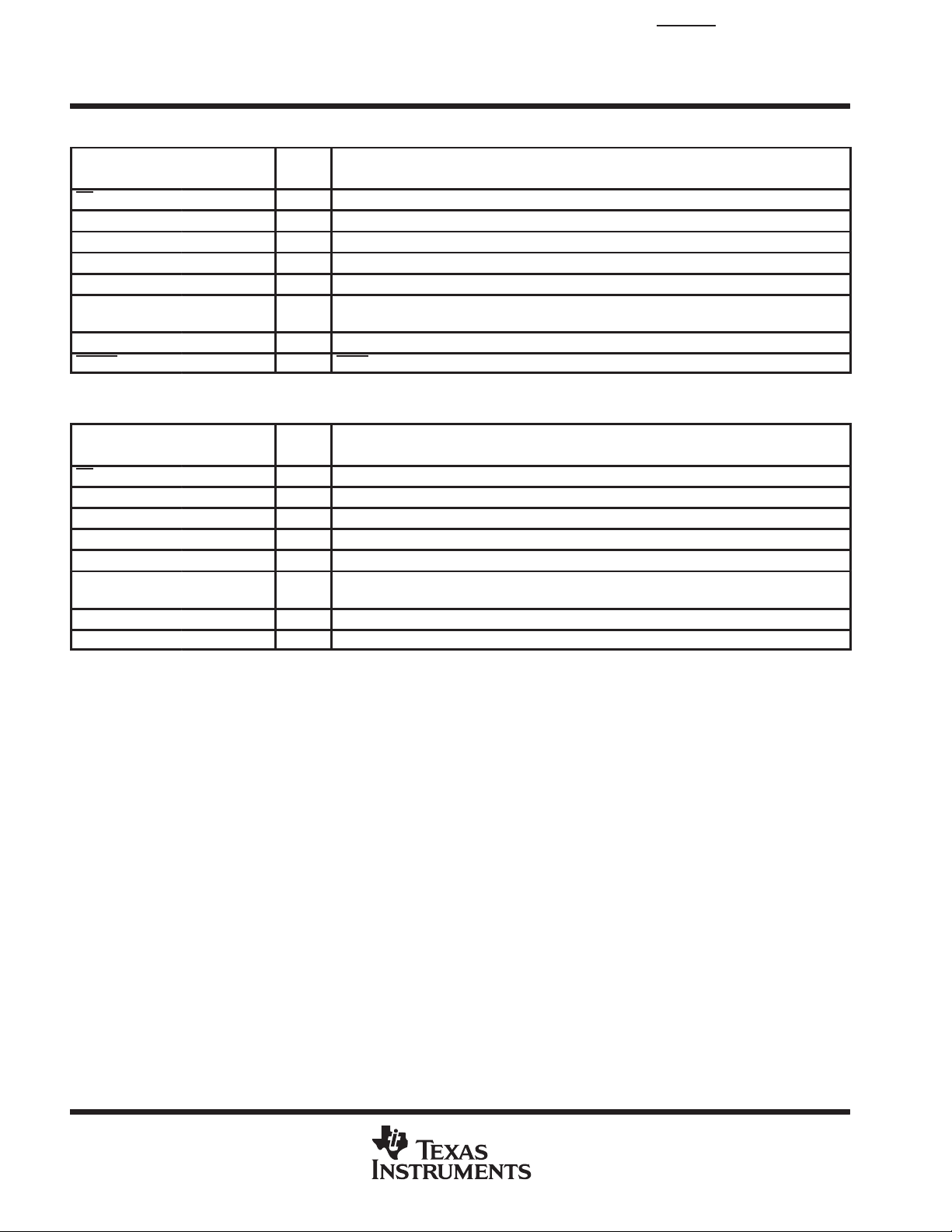
Terminal Functions (TPS752xxQ)
TERMINAL
NAME NO.
EN 5 I Enable Input
FB/SENSE 7 I Feedback input voltage for adjustable device (sense input for fixed-voltage option)
GND 17 Regulator ground
GND/HEATSINK 1, 10, 11, 20 Ground/heatsink
IN 3, 4 I Input voltage
NC 2, 12, 13, 14,
15, 16, 18, 19
OUTPUT 8, 9 O Regulated output voltage
RESET 6 O Reset output
TERMINAL
NAME NO.
EN 5 I Enable Input
FB/SENSE 7 I Feedback input voltage for adjustable device (sense input for fixed-voltage option)
GND 17 Regulator ground
GND/HEATSINK 1, 10, 11, 20 Ground/heatsink
IN 3, 4 I Input voltage
NC 2, 12, 13, 14,
15, 16, 18, 19
OUTPUT 8, 9 O Regulated output voltage
PG 6 O Power good output
No connection
Terminal Functions (TPS754xxQ)
No connection
4
POST OFFICE BOX 655303 • DALLAS, TEXAS 75265
TPS75201Q, TPS75215Q, TPS75218Q, TPS75225Q, TPS75233Q WITH RESET
TPS75401Q, TPS75415Q, TPS75418Q, TPS75425Q, TPS75433Q WITH POWER GOOD
FAST-TRANSIENT-RESPONSE 2-A LOW-DROPOUT VOLTAGE REGULATORS
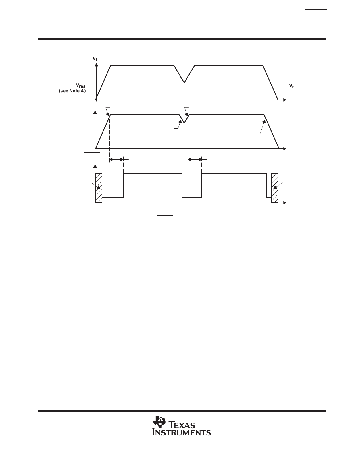
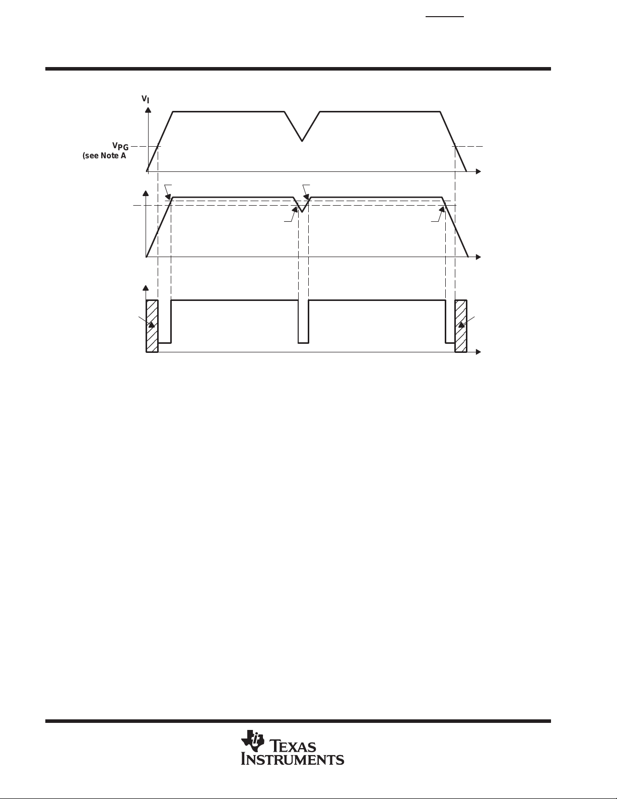
TPS752xxQ RESET timing diagram
V
I
SLVS242 – MARCH 2000
(see Note A)
Threshold
NOTES: A. V
B. VIT –Trip voltage is typically 5% lower than the output voltage (95%VO) V
V
res
V
O
Voltage
RESET
Output
Output
Undefined
is the minimum input voltage for a valid RESET
res
for semiconductor symbology.
V
(see Note B)
IT+
V
IT–
100 ms
Delay
(see Note B)
V
IT+
Less than 5% of the
output voltage
. The symbol V
V
res
t
(see Note B)
V
(see Note B)
IT–
t
100 ms
Delay
Output
Undefined
t
is not currently listed within EIA or JEDEC standards
res
to V
IT–
is the hysteresis voltage.
IT+
POST OFFICE BOX 655303 • DALLAS, TEXAS 75265
5
TPS75201Q, TPS75215Q, TPS75218Q, TPS75225Q, TPS75233Q WITH RESET
TPS75401Q, TPS75415Q, TPS75418Q, TPS75425Q, TPS75433Q WITH POWER GOOD
FAST-TRANSIENT-RESPONSE 2-A LOW-DROPOUT VOLTAGE REGULATORS
SLVS242 – MARCH 2000
TPS754xxQ PG timing diagram
V
I
V
(see Note A)
NOTES: A. VPG is the minimum input voltage for a valid PG. The symbol VPG is not currently listed within EIA or JEDEC standards for
B. VIT –Trip voltage is typically 17% lower than the output voltage (83%VO) V
PG
V
O
Threshold
Voltage
PG
Output
Output
Undefined
semiconductor symbology .
V
(see Note B)
IT+
V
(see Note B)
IT–
V
(see Note B)
IT+
V
(see Note B)
IT–
to V
IT–
is the hysteresis voltage.
IT+
V
PG
t
t
Output
Undefined
t
6
POST OFFICE BOX 655303 • DALLAS, TEXAS 75265
PWP
§
PWP
¶
TPS75201Q, TPS75215Q, TPS75218Q, TPS75225Q, TPS75233Q WITH RESET
TPS75401Q, TPS75415Q, TPS75418Q, TPS75425Q, TPS75433Q WITH POWER GOOD
FAST-TRANSIENT-RESPONSE 2-A LOW-DROPOUT VOLTAGE REGULATORS
SLVS242 – MARCH 2000
absolute maximum ratings over operating junction temperature range
(unless otherwise noted)
Input voltage range‡, VI –0.3 V to 5.5 V. . . . . . . . . . . . . . . . . . . . . . . . . . . . . . . . . . . . . . . . . . . . . . . . . . . . . . . . . . . .
Voltage range at EN –0.3 V to 16.5 V. . . . . . . . . . . . . . . . . . . . . . . . . . . . . . . . . . . . . . . . . . . . . . . . . . . . . . . . . . . . . .
Maximum RESET voltage (TPS752xxQ) 16.5 V. . . . . . . . . . . . . . . . . . . . . . . . . . . . . . . . . . . . . . . . . . . . . . . . . . . .
Maximum PG voltage (TPS754xxQ) 16.5 V. . . . . . . . . . . . . . . . . . . . . . . . . . . . . . . . . . . . . . . . . . . . . . . . . . . . . . . .
Peak output current Internally limited. . . . . . . . . . . . . . . . . . . . . . . . . . . . . . . . . . . . . . . . . . . . . . . . . . . . . . . . . . . . . .
Output voltage, V
Continuous total power dissipation See dissipation rating tables. . . . . . . . . . . . . . . . . . . . . . . . . . . . . . . . . . . . . .
Operating virtual junction temperature range, TJ –40°C to 125°C. . . . . . . . . . . . . . . . . . . . . . . . . . . . . . . . . . . . .
Storage temperature range, T
ESD rating, HBM 2 kV. . . . . . . . . . . . . . . . . . . . . . . . . . . . . . . . . . . . . . . . . . . . . . . . . . . . . . . . . . . . . . . . . . . . . . . . . .
†
Stresses beyond those listed under “absolute maximum ratings” may cause permanent damage to the device. These are stress ratings only, and
functional operation of the device at these or any other conditions beyond those indicated under “recommended operating conditions” is not
implied. Exposure to absolute-maximum-rated conditions for extended periods may affect device reliability.
‡
All voltage values are with respect to network terminal ground.
PACKAGE
§
This parameter is measured with the recommended copper heat sink pattern on a 1-layer PCB, 5-in × 5-in PCB, 1 oz. copper, 2-in × 2-in coverage
(4 in2).
¶
This parameter is measured with the recommended copper heat sink pattern on a 8-layer PCB, 1.5-in × 2-in PCB, 1 oz. copper with layers 1,
2, 4, 5, 7, and 8 at 5% coverage (0.9 in2) and layers 3 and 6 at 100% coverage (6 in2). For more information, refer to TI technical brief SLMA002.
(OUTPUT, FB) 5.5 V. . . . . . . . . . . . . . . . . . . . . . . . . . . . . . . . . . . . . . . . . . . . . . . . . . . . . . . . . .
O
–65°C to 150°C. . . . . . . . . . . . . . . . . . . . . . . . . . . . . . . . . . . . . . . . . . . . . . . . . . .
stg
DISSIPATION RATING TABLE 1 – FREE-AIR TEMPERATURES
AIR FLOW
(CFM)
0 2.9 W 23.5 mW/°C 1.9 W 1.5 W
300 4.3 W 34.6 mW/°C 2.8 W 2.2 W
0 3 W 23.8 mW/°C 1.9 W 1.5 W
300 7.2 W 57.9 mW/°C 4.6 W 3.8 W
TA < 25°C
POWER RATING
DERATING FACTOR
ABOVE TA = 25°C
Ĕ
TA = 70°C
POWER RATING
TA = 85°C
POWER RATING
recommended operating conditions
Input voltage, V
Output voltage range, V
Output current, I
Operating virtual junction temperature, T
#
To calculate the minimum input voltage for your maximum output current, use the following equation: V
#
I
O
O
J
I(min)
MIN MAX UNIT
2.7 5 V
1.5 5 V
0 2.0 A
–40 125 °C
= V
O(max)
+ V
DO(max load)
.
POST OFFICE BOX 655303 • DALLAS, TEXAS 75265
7
TPS75201Q, TPS75215Q, TPS75218Q, TPS75225Q, TPS75233Q WITH RESET
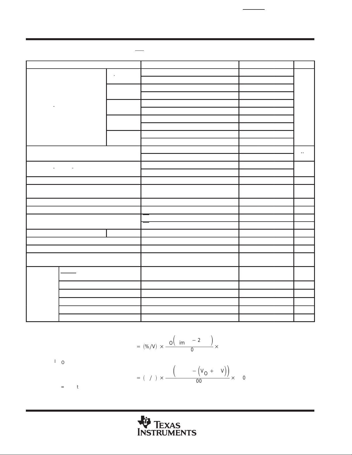
j
1.5 V Output
g
1.8 V Output
V
2.5 V Output
3.3 V Output
Quiescent current (GND current) (see Note 1)
A
gg(
OO
)
%/V
Standby current
(TPS752xxQ)
TPS75401Q, TPS75415Q, TPS75418Q, TPS75425Q, TPS75433Q WITH POWER GOOD
FAST-TRANSIENT-RESPONSE 2-A LOW-DROPOUT VOLTAGE REGULATORS
SLVS242 – MARCH 2000
electrical characteristics over recommended operating junction temperature range (TJ = –40°C to
125°C), V
Output voltage
(see Notes 1 and 3)
Output voltage line regulation (∆V
(see Notes 1 and 2)
Load regulation (see Note 3) 1 mV
Output noise voltage
Output current Limit VO = 0 V 3.3 4.5 A
Thermal shutdown junction temperature 150 °C
FB input current TPS75x01Q FB = 1.5 V –1 1 µA
High level enable input voltage 2 V
Low level enable input voltage 0.7 V
Power supply ripple rejection (see Note 2)
Reset
NOTES: 1. Minimum IN operating voltage is 2.7 V or V
= V
I
Minimum input voltage for valid
RESET
Trip threshold voltage VO decreasing 92 98 %V
Hysteresis voltage Measured at V
Output low voltage VI = 2.7 V, I
Leakage current V
RESET time-out delay 100 ms
2. If VO≤ 1.8 V then V
+ 1 V, IO = 1 mA, EN = 0 V, CO = 47 µF (unless otherwise noted)
O(typ)
PARAMETER TEST CONDITIONS MIN TYP MAX UNIT
Adjustable
Voltage
/V
= 2.7 V, V
imin
imax
Line Reg. (mV)
1.5 V ≤ VO ≤ 5 V, TJ = 25°C V
1.5 V ≤ VO ≤ 5 V 0.98V
TJ = 25°C, 2.7 V < VIN < 5 V 1.5
p
2.7 V < VIN < 5 V 1.470 1.530
TJ = 25°C, 2.8 V < VIN < 5 V 1.8
p
2.8 V < VIN < 5 V 1.764 1.836
TJ = 25°C, 3.5 V < VIN < 5 V 2.5
p
3.5 V < VIN < 5 V 2.450 2.550
TJ = 25°C, 4.3 V < VIN < 5 V 3.3
p
4.3 V < VIN < 5 V 3.234 3.366
TJ = 25°C, See Note 3 75
See Note 3 125
VO + 1 V < VI ≤ 5 V, TJ = 25°C, 0.01
VO + 1 V < VI < 5 V 0.1
BW = 300 Hz to 50 kHz, VO = 1.5 V
CO = 100 µF, TJ = 25°C
EN = V
I,
EN = V
I
f = 100 Hz, CO = 100 µF,
TJ = 25°C, See Note 1, IO = 2 A
I
O(RESET)
(RESET)
O(typ)
= 5 V:
+ǒ%ńVǓ
= 300µA, V
O
= 5 V 1 µA
+ 1 V, whichever is greater. Maximum IN voltage 5V.
ǒ
V
O
TJ = 25°C, 1 µA
≤ 0.8 V 1 1.3 V
= 1 mA 0.15 0.4 V
Ǔ
2.7 V
1000
V
imax
100
(RESET)
O(RESET)
*
O
O
1.02V
O
60 µVrms
10 µA
60 dB
0.5 %V
µ
O
O
If V
≥ 2.5 V then V
O
3. IO = 1 mA to 2 A
8
= VO + 1 V, V
imin
Line Reg. (mV)
POST OFFICE BOX 655303 • DALLAS, TEXAS 75265
= 5 V:
imax
+ǒ%ńVǓ
ǒ
V
V
*ǒVO)
imax
O
100
1V
Ǔ
Ǔ
1000
(TPS754xxQ)
Input current (EN)
g( )( )
VOOutput voltage
VDODropout voltage
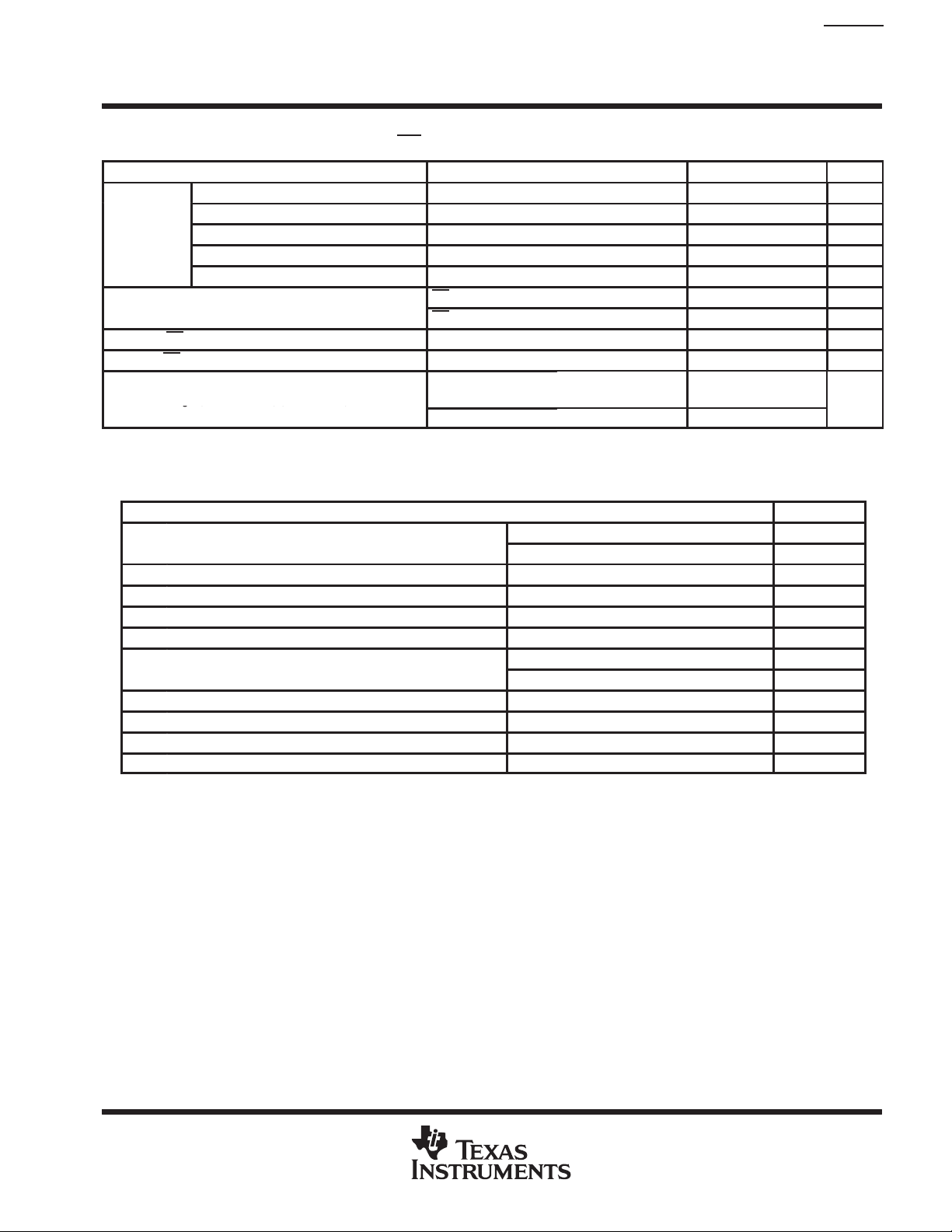
TPS75201Q, TPS75215Q, TPS75218Q, TPS75225Q, TPS75233Q WITH RESET
TPS75401Q, TPS75415Q, TPS75418Q, TPS75425Q, TPS75433Q WITH POWER GOOD
FAST-TRANSIENT-RESPONSE 2-A LOW-DROPOUT VOLTAGE REGULATORS
SLVS242 – MARCH 2000
electrical characteristics over recommended operating junction temperature range (TJ = –40°C to
125°C), V
PG
p
High level EN input voltage 2 V
Low level EN input voltage 0.7 V
Dropout voltage (3.3 V Output) (see Note 4)
NOTE 4: IN voltage equals VO(Typ) – 100 mV; TPS75x15Q, TPS75x18Q and TPS75x25Q dropout voltage limited by input voltage range
Z
V
= V
I
Minimum input voltage for valid PG I
Trip threshold voltage VO decreasing 80 86 %V
Hysteresis voltage Measured at V
Output low voltage I
Leakage current V
limitations (i.e., TPS75x33Q input voltage needs to drop to 3.2 V for purpose of this test).
+ 1 V, I
O(typ)
PARAMETER TEST CONDITIONS
= 1 mA, EN = 0 V, CO = 47 µF (unless otherwise noted) (continued)
O
= 300 µA V(PG) ≤ 0.8 V 1.1 1.3 V
O(PG)
O
= 1 mA 0.15 0.4 V
O(PG)
= 5.5 V 1 µA
(PG)
EN = V
I
EN = 0 V –1 0 1 µA
IO = 2 A,
TJ = 25°C
IO = 2 A, VI = 3.2 V 400
VI = 3.2 V,
MIN TYP MAX UNIT
–1 1 µA
Table of Graphs
p
Ground current vs Junction temperature 6
Power supply ripple rejection vs Frequency 7
Output spectral noise density vs Frequency 8
Output impedance vs Frequency 9
o
p
Line transient response 12, 14
Load transient response 13, 15
Output voltage vs Time 16
O
Equivalent series resistance (ESR) vs Output current 18, 19
vs Output current 2, 3
vs Junction temperature 4, 5,
vs Input voltage 10
vs Junction temperature 11
0.5 %V
210
FIGURE
O
O
mV
POST OFFICE BOX 655303 • DALLAS, TEXAS 75265
9
 Loading...