


TPS65930/TPS65920
Integrated Power Management
\Audio Codec (TPS65930 Only)
Silicon Revision 1.2
Data Manual
PRODUCTION DATA information is current as of publication date.
Products conform to specifications per the terms of the Texas
Instruments standard warranty. Production processing does not
necessarily include testing of all parameters.
Literature Number: SWCS037G
May 2008–Revised April 2011
TPS65930/TPS65920
SWCS037G–MAY 2008– REVISED APRIL 2011
www.ti.com
Contents
1 Introduction ........................................................................................................................ 9
1.1 Features .................................................................................................................... 10
1.2 TPS65920 and TPS65930 Device Block Diagrams ................................................................... 11
2 Terminal Description .......................................................................................................... 13
2.1 Ball Characteristics ........................................................................................................ 13
2.2 Signal Description ......................................................................................................... 17
3 Electrical Characteristics .................................................................................................... 23
3.1 Absolute Maximum Ratings .............................................................................................. 23
3.2 Minimum Voltages and Associated Currents .......................................................................... 23
3.3 Recommended Operating Conditions .................................................................................. 24
3.4 Digital I/O Electrical Characteristics ..................................................................................... 24
4 Power Module ................................................................................................................... 27
4.1 Power Providers ........................................................................................................... 28
4.1.1 VDD1 dc-dc Regulator ......................................................................................... 29
4.1.1.1 VDD1 dc-dc Regulator Characteristics .......................................................... 29
4.1.1.2 External Components and Application Schematics ........................................... 30
4.1.2 VDD2 dc-dc Regulator ......................................................................................... 32
4.1.2.1 VDD2 dc-dc Regulator Characteristics .......................................................... 32
4.1.2.2 External Components and Application Schematics ........................................... 33
4.1.3 VIO dc-dc Regulator ............................................................................................ 35
4.1.3.1 VIO dc-dc Regulator Characteristics ............................................................ 35
4.1.3.2 External Components and Application Schematics ........................................... 36
4.1.4 VDAC LDO Regulator .......................................................................................... 38
4.1.5 VPLL1 LDO Regulator ......................................................................................... 39
4.1.6 VMMC1 LDO Regulator ....................................................................................... 40
4.1.7 VAUX2 LDO Regulator ........................................................................................ 41
4.1.8 Output Load Conditions ........................................................................................ 42
4.1.9 Charge Pump ................................................................................................... 43
4.1.10 USB LDO Short-Circuit Protection Scheme ................................................................. 44
4.2 Power References ......................................................................................................... 45
4.3 Power Control .............................................................................................................. 45
4.3.1 Backup Battery Charger ....................................................................................... 45
4.3.2 Battery Monitoring and Threshold Detection ................................................................ 46
4.3.2.1 Power On/Power Off and Backup Conditions .................................................. 46
4.3.3 VRRTC LDO Regulator ........................................................................................ 46
4.4 Power Consumption ....................................................................................................... 47
4.5 Power Management ....................................................................................................... 49
4.5.1 Boot Modes ...................................................................................................... 49
4.5.2 Process Modes .................................................................................................. 49
4.5.2.1 MC021 Mode ....................................................................................... 49
4.5.3 Power-On Sequence ........................................................................................... 49
4.5.3.1 Timing Before Sequence_Start .................................................................. 49
4.5.3.2 Power-On Sequence .............................................................................. 51
4.5.3.3 Power On in Slave_C021 Mode ................................................................. 51
4.5.4 Power-Off Sequence ........................................................................................... 53
4.5.4.1 Power-Off Sequence .............................................................................. 53
2 Contents Copyright © 2008–2011, Texas Instruments Incorporated
TPS65930/TPS65920
www.ti.com
SWCS037G–MAY 2008– REVISED APRIL 2011
5 Real-Time Clock and Embedded Power Controller ................................................................. 54
5.1 RTC ......................................................................................................................... 54
5.1.1 Backup Battery .................................................................................................. 54
5.2 EPC ......................................................................................................................... 54
6 Audio/Voice Module (TPS65930 Device Only) ........................................................................ 55
6.1 Audio/Voice Downlink (RX) Module ..................................................................................... 55
6.1.1 Predriver for External Class-D Amplifier ..................................................................... 55
6.1.1.1 Predriver Output Characteristics ................................................................. 56
6.1.1.2 External Components and Application Schematics ........................................... 56
6.1.2 Vibrator H-Bridge ............................................................................................... 57
6.1.2.1 Vibrator H-Bridge Output Characteristics ....................................................... 57
6.1.2.2 External Components and Application Schematics ........................................... 57
6.1.3 Carkit Output .................................................................................................... 58
6.1.4 Digital Audio Filter Module .................................................................................... 59
6.1.5 Boost Stage ..................................................................................................... 59
6.2 Audio Uplink (TX) Module ................................................................................................ 61
6.2.1 Microphone Bias Module ...................................................................................... 61
6.2.1.1 Analog Microphone Bias Module Characteristics .............................................. 61
6.2.1.2 Silicon Microphone Module Characteristics .................................................... 63
6.2.2 FM Radio/Auxiliary Input ....................................................................................... 65
6.2.2.1 External Components ............................................................................. 65
6.2.3 Uplink Characteristics .......................................................................................... 65
6.2.4 Microphone Amplification Stage .............................................................................. 66
6.2.5 Carkit Input ...................................................................................................... 67
6.2.6 Digital Audio Filter Module .................................................................................... 68
7 USB Transceiver ............................................................................................................... 69
7.1 USB Transceiver ........................................................................................................... 69
7.1.1 Features ......................................................................................................... 69
7.1.2 HS USB Port Timing ........................................................................................... 70
7.1.3 USB-CEA Carkit Port Timing .................................................................................. 71
7.1.4 PHY Electrical Characteristics ................................................................................ 73
7.1.4.1 HS Differential Receiver ........................................................................... 73
7.1.4.2 HS Differential Transmitter ........................................................................ 74
7.1.4.3 CEA/UART Driver .................................................................................. 75
7.1.4.4 Pullup/Pulldown Resistors ........................................................................ 75
7.1.5 OTG Electrical Characteristics ................................................................................ 75
7.1.5.1 OTG VBUS Electrical Characteristics ........................................................... 76
7.1.5.2 OTG ID Electrical Characteristics ................................................................ 76
8 MADC ............................................................................................................................... 78
8.1 General Description ....................................................................................................... 78
8.2 MADC Electrical Characteristics ......................................................................................... 78
8.3 Channel Voltage Input Range ........................................................................................... 79
8.3.1 Sequence Conversion Time (Real-Time or Nonaborted Asynchronous) ................................ 79
9 LED Drivers ...................................................................................................................... 81
9.1 General Description ....................................................................................................... 81
10 Keyboard .......................................................................................................................... 82
10.1 Keyboard Connection ..................................................................................................... 82
11 Clock Specifications .......................................................................................................... 83
Copyright © 2008–2011, Texas Instruments Incorporated Contents 3
TPS65930/TPS65920
SWCS037G–MAY 2008– REVISED APRIL 2011
11.1 Clock Features ............................................................................................................. 83
11.2 Input Clock Specifications ................................................................................................ 84
11.2.1 Clock Source Requirements .................................................................................. 84
11.2.2 HFCLKIN ......................................................................................................... 84
11.2.3 32-kHz Input Clock ............................................................................................. 86
11.2.3.1 External Crystal Description ...................................................................... 87
11.2.3.2 External Clock Description ........................................................................ 88
11.3 Output Clock Specifications .............................................................................................. 91
11.3.1 32KCLKOUT Output Clock .................................................................................... 91
11.3.2 HFCLKOUT Output Clock ..................................................................................... 92
11.3.3 Output Clock Stabilization Time .............................................................................. 93
www.ti.com
12 Timing Requirements and Switching Characteristics ............................................................. 94
12.1 Timing Parameters ........................................................................................................ 94
12.2 Target Frequencies ........................................................................................................ 95
12.3 I
12.4 Audio Interface: TDM/I2S Protocol ...................................................................................... 97
12.5 JTAG Interfaces .......................................................................................................... 101
2
C Timing .................................................................................................................. 96
12.4.1 I2S Right- and Left-Justified Data Format ................................................................... 98
12.4.2 TDM Data Format ............................................................................................. 100
13 Debouncing Time ............................................................................................................. 103
14 External Components ....................................................................................................... 104
15 TPS65920/TPS65930 Package ............................................................................................ 107
15.1 TPS65920/TPS65930 Standard Package Symbols ................................................................. 107
15.2 Package Thermal Resistance Characteristics ....................................................................... 107
15.3 Mechanical Data ......................................................................................................... 108
15.4 ESD Specifications ...................................................................................................... 109
16 Glossary ......................................................................................................................... 110
4 Contents Copyright © 2008–2011, Texas Instruments Incorporated

TPS65930/TPS65920
www.ti.com
SWCS037G–MAY 2008– REVISED APRIL 2011
List of Figures
1-1 TPS65920 Block Diagram....................................................................................................... 12
1-2 TPS65930 Block Diagram....................................................................................................... 12
2-1 PBGA Bottom View .............................................................................................................. 13
4-1 Power Provider Block Diagram................................................................................................. 27
4-2 VDD1 dc-dc Regulator Efficiency .............................................................................................. 30
4-3 VDD1 dc-dc Application Schematic............................................................................................ 31
4-4 VDD2 dc-dc Regulator Efficiency .............................................................................................. 33
4-5 VDD2 dc-dc Application Schematic............................................................................................ 34
4-6 VIO dc-dc Regulator Efficiency................................................................................................. 36
4-7 VIO dc-dc Application Schematic .............................................................................................. 37
4-8 Timing Before Sequence Start ................................................................................................. 50
4-9 Timings–Power On in OMAP3 Mode.......................................................................................... 51
4-10 Timings—Power On in Slave_C021 Mode.................................................................................... 52
4-11 Power-Off Sequence in Master Modes ....................................................................................... 53
6-1 Audio/Voice Module Block Diagram ........................................................................................... 55
6-2 Predriver for External Class D.................................................................................................. 57
6-3 Vibrator H-Bridge................................................................................................................. 58
6-4 Carkit Output Downlink Path Characteristics................................................................................. 58
6-5 Digital Audio Filter Downlink Path Characteristics........................................................................... 59
6-6 Analog Microphone Pseudodifferential ........................................................................................ 62
6-7 Analog Microphone Differential................................................................................................. 63
6-8 Silicon Microphone ............................................................................................................... 64
6-9 Audio Auxiliary Input ............................................................................................................. 65
6-10 Uplink Amplifier................................................................................................................... 65
6-11 Carkit Input Uplink Path Characteristics ...................................................................................... 67
6-12 Digital Audio Filter Uplink Path Characteristics .............................................................................. 68
7-1 USB 2.0 PHY Block Diagram................................................................................................... 69
7-2 USB System Application Schematic........................................................................................... 70
7-3 HS-USB Interface—Transmit and Receive Modes (ULPI 8-bit)............................................................ 71
7-4 USB-CEA Carkit UART Data Flow............................................................................................. 72
7-5 USB-CEA Carkit UART Timings................................................................................................ 73
8-1 Conversion Sequence General Timing Diagram............................................................................. 80
9-1 LED Driver Block Diagram ...................................................................................................... 81
10-1 Keyboard Connection............................................................................................................ 82
11-1 Clock Overview................................................................................................................... 83
11-2 HFCLKIN Clock Distribution .................................................................................................... 84
11-3 Example of Wired-OR Clock Request ......................................................................................... 85
11-4 HFCLKIN Squared Input Clock................................................................................................. 86
11-5 32-kHz Oscillator Block Diagram In Master Mode With Crystal............................................................ 87
11-6 32-kHz Crystal Input ............................................................................................................. 88
11-7 32-kHz Oscillator Block Diagram Without Crystal Option 1................................................................. 89
11-8 32-kHz Oscillator Block Diagram Without Crystal Option 2................................................................. 90
11-9 32-kHz Oscillator in Bypass Mode Block Diagram Without Crystal Option 3 ............................................ 90
11-10 32-kHz Square- or Sine-Wave Input Clock ................................................................................... 91
11-11 32.768-kHz Clock Output Block Diagram ..................................................................................... 91
11-12 32KCLKOUT Output Clock...................................................................................................... 92
11-13 HFCLKOUT Output Clock....................................................................................................... 93
Copyright © 2008–2011, Texas Instruments Incorporated List of Figures 5
TPS65930/TPS65920
SWCS037G–MAY 2008– REVISED APRIL 2011
www.ti.com
11-14 32KCLKOUT and HFCLKOUT Clock Stabilization Time.................................................................... 93
11-15 HFCLKOUT Behavior ........................................................................................................... 93
12-1 I
2
C Interface—Transmit and Receive in Slave Mode........................................................................ 96
12-2 I2S Interface—I2S Master ModeI .............................................................................................. 98
12-3 I2S Interface—I2S Slave Mode................................................................................................. 98
12-4 TDM Interface—TDM Master Mode.......................................................................................... 100
12-5 JTAG Interface Timing ......................................................................................................... 102
13-1 Debouncing Sequence Chronogram Example.............................................................................. 103
15-1 Printed Device Reference ..................................................................................................... 107
15-2 TPS65920/TPS65930 Mechanical Package Bottom View ................................................................ 108
15-3 Ball Size.......................................................................................................................... 108
6 List of Figures Copyright © 2008–2011, Texas Instruments Incorporated
TPS65930/TPS65920
www.ti.com
SWCS037G–MAY 2008– REVISED APRIL 2011
List of Tables
2-1 Ball Characteristics............................................................................................................... 13
2-2 Signal Description ................................................................................................................ 17
3-1 Absolute Maximum Ratings..................................................................................................... 23
3-2 VBAT Minimum Required Per VBAT Ball and Associated Maximum Current ........................................... 23
3-3 Recommended Operating Maximum Ratings ................................................................................ 24
3-4 Digital I/O Electrical Characteristics ........................................................................................... 24
4-1 Summary of the Power Providers.............................................................................................. 28
4-2 Part Names With Corresponding VDD1 Current Support................................................................... 29
4-3 VDD1 dc-dc Regulator Characteristics........................................................................................ 29
4-4 VDD2 dc-dc Regulator Characteristics........................................................................................ 32
4-5 VIO dc-dc Regulator Characteristics........................................................................................... 35
4-6 VDAC LDO Regulator Characteristics......................................................................................... 38
4-7 VPLL1 LDO Regulator Characteristics ........................................................................................ 39
4-8 VMMC1 LDO Regulator Characteristics....................................................................................... 40
4-9 VAUX2 LDO Regulator Characteristics ....................................................................................... 41
4-10 Output Load Conditions ......................................................................................................... 42
4-11 Charge Pump Output Load Conditions........................................................................................ 43
4-12 Voltage Reference Characteristics............................................................................................. 45
4-13 Backup Battery Charger Characteristics ...................................................................................... 45
4-14 Battery Threshold Levels........................................................................................................ 46
4-15 VRRTC LDO Regulator Characteristics....................................................................................... 46
4-16 Power Consumption ............................................................................................................. 47
4-17 Regulator State Depending on Use Case..................................................................................... 48
4-18 BOOT Mode Description ........................................................................................................ 49
4-19 MC021 Mode...................................................................................................................... 49
5-1 System States .................................................................................................................... 54
6-1 Predriver Output Characteristics ............................................................................................... 56
6-2 Vibrator H-Bridge Output Characteristics ..................................................................................... 57
6-3 USB-CEA Carkit Audio Downlink Electrical Characteristics................................................................ 58
6-4 Digital Audio Filter RX Electrical Characteristics............................................................................. 59
6-5 Boost Electrical Characteristics Versus FSFrequency (F
6-6 Boost Electrical Characteristics Versus FSFrequency (F
6-7 Analog Microphone Bias Module Characteristics With Bias Resistor ..................................................... 61
6-8 Analog Microphone Bias Module Characteristics With Bias Resistor ..................................................... 61
6-9 Silicon Microphone Module Characteristics................................................................................... 64
6-10 Uplink Characteristics............................................................................................................ 65
6-11 USB-CEA Carkit Audio Uplink Electrical Characteristics.................................................................... 67
6-12 Digital Audio Filter TX Electrical Characteristics ............................................................................. 68
7-1 HS-USB Interface Timing Requirements...................................................................................... 71
7-2 HS-USB Interface Switching Requirements .................................................................................. 71
7-3 USB-CEA Carkit Interface Timing Parameters............................................................................... 72
7-4 USB-CEA Carkit UART Timings................................................................................................ 73
7-5 HS Differential Receiver......................................................................................................... 74
7-6 HS Differential Transmitter...................................................................................................... 74
7-7 CEA/UART Driver ................................................................................................................ 75
7-8 Pullup/Pulldown Resistors....................................................................................................... 75
7-9 OTG VBUS Electrical Characteristics ......................................................................................... 76
Copyright © 2008–2011, Texas Instruments Incorporated List of Tables 7
≤ 22.05 kHz) ................................................. 60
S
≥ 24 kHz)..................................................... 60
S

TPS65930/TPS65920
SWCS037G–MAY 2008– REVISED APRIL 2011
www.ti.com
7-10 OTG ID Electrical Characteristics.............................................................................................. 76
8-1 MADC Electrical Characteristics ............................................................................................... 78
8-2 Analog Input Voltage Range.................................................................................................... 79
8-3 Sequence Conversion Timing Characteristics................................................................................ 79
9-1 LED Driver Electrical Characteristics .......................................................................................... 81
11-1 TPS65920/TPS65930 Input Clock Source Requirements .................................................................. 84
11-2 HFCLKIN Input Clock Electrical Characteristics ............................................................................. 86
11-3 HFCLKIN Square Input Clock Timing Requirements with Slicer in Bypass.............................................. 86
11-4 Crystal Electrical Characteristics............................................................................................... 87
11-5 Base Oscillator Switching Characteristics..................................................................................... 88
11-6 32-kHz Crystal Input Clock Timing Requirements ........................................................................... 88
11-7 32-kHz Input Square- or Sine-Wave Clock Source Electrical Characteristics............................................ 90
11-8 32-kHz Square-Wave Input Clock Source Timing Requirements.......................................................... 90
11-9 32KCLKOUT Output Clock Electrical Characteristics ....................................................................... 92
11-10 32KCLKOUT Output Clock Switching Characteristics....................................................................... 92
11-11 HFCLKOUT Output Clock Electrical Characteristics ........................................................................ 92
11-12 HFCLKOUT Output Clock Switching Characteristics........................................................................ 92
12-1 Timing Parameters............................................................................................................... 94
12-2 TPS65920/TPS65930 Interface Target Frequencies........................................................................ 95
12-3 I
12-4 I
2
C Interface—Timing Requirements .......................................................................................... 96
2
C Interface—Switching Requirements ...................................................................................... 97
12-5 I2S Interface—Timing Requirements.......................................................................................... 99
12-6 I2S Interface—Switching Characteristics...................................................................................... 99
12-7 TDM Interface Master Mode—Timing Requirements ...................................................................... 101
12-8 TDM Interface Master Mode—Switching Characteristics ................................................................. 101
12-9 JTAG Interface—Timing Requirements...................................................................................... 102
12-10 JTAG Interface—Switching Characteristics ................................................................................. 102
13-1 Debouncing...................................................................................................................... 103
14-1 TPS65920/TPS65930 External Components ............................................................................... 104
15-1 TPS65920/TPS65930 Nomenclature Description .......................................................................... 107
15-2 TPS65920 Thermal Resistance Characteristics............................................................................ 107
15-3 TPS65930 Thermal Resistance Characteristics............................................................................ 107
8 List of Tables Copyright © 2008–2011, Texas Instruments Incorporated
TPS65930/TPS65920
www.ti.com
1 Introduction
The TPS65920/TPS65930 devices are power-management ICs for OMAP™ and other mobile
applications. The devices include power-management, a universal serial bus (USB) high-speed (HS)
transceiver, light -emitting diode (LED) drivers, an analog-to-digital converter (ADC), a real-time clock
(RTC), and embedded power control (EPC). In addition, the TPS65930 includes a full audio codec with
two digital-to-analog converters (DACs) and two ADCs to implement dual voice channels, and a stereo
downlink channel that can play all standard audio sample rates through a multiple format inter-integrated
sound (I2S™)/time division multiplexing (TDM) interface.
These optimized devices support the power and peripheral requirements of the OMAP application
processors. The power portion of the devices contains three buck converters, two controllable by a
dedicated SmartReflex™ class-3 interface, multiple low dropout (LDO) regulators, an EPC to manage the
power sequencing requirements of OMAP, and an RTC and backup module. The RTC can be powered by
a backup battery when the main supply is not present, and the devices include a coin-cell charger to
recharge the backup battery as needed.
The USB module provides a HS 2.0 OTG transceiver suitable for direct connection to the OMAP UTMI+
low pin interface (ULPI), with an integrated charge pump and full support for the carkit CEA-936A
specification. An ADC is provided for monitoring signals, such as supply voltage, entering the device, and
two additional external ADC inputs are provided for system use.
SWCS037G–MAY 2008– REVISED APRIL 2011
Integrated Power Management
\Audio Codec (TPS65930 Only)
Check for Samples: TPS65930/TPS65920
The devices provide driver circuitry to power two LED circuits that can illuminate a panel or provide user
indicators. The drivers also provide pulse width modulation (PWM) circuits to control the illumination levels
of the LEDs. A keypad interface implements a built-in scanning algorithm to decode hardware-based key
presses and reduce software use, with multiple additional general-purpose input/output devices (GPIOs)
that can be used as interrupts when configured as inputs.
This TPS65920/TPS65930 data manual presents the electrical and mechanical specifications for the
TPS65920 and TPS65930 devices . It covers the following topics:
• TPS65920/TPS65930 terminals: Assignment, multiplexing, electrical characteristics, and functional
description (see Section 2, Terminal Description)
• Electrical characteristic requirements: Maximum and recommended operating conditions, digital
input/output (I/O) characteristics (see Section 3, Electrical Characteristics)
• Power module: Power provider, power references, power control, power consumption, and power
management, with the on and off sequence (see Section 4, Power Module)
• RTC and EPC (see Section 5, Real-Time Clock and Embedded Power Controller)
• Audio/voice module (TPS65930 device only): Electrical characteristics and application schematics for
the downlink and uplink paths (see Section 6, Audio/Voice Module (TPS65930 Device Only))
• Various modules: USB transceiver, monitoring analog-to-digital converter (MADC), LED drivers, and
keyboard (see Section 8, MADC, Section 9, LED Driver, and Section 10, Keyboard)
• Clock specifications: Clock slicer; input and output clocks (see Section 11, Clock Specifications)
• Timing requirements and switching characteristics (ac timings) of the interfaces (see Section 12,
Timing Requirements and Switching Characteristics)
• Debouncing time (see Section 13, Debouncing Time)
• External components for the application schematics (see Section 14, External Components)
• Thermal resistance characteristics, device nomenclature, and mechanical data about the available
packaging (see Section 15, TPS65920/TPS65930 Package )
PRODUCTION DATA information is current as of publication date.
Products conform to specifications per the terms of the Texas
Instruments standard warranty. Production processing does not
necessarily include testing of all parameters.
Copyright © 2008–2011, Texas Instruments Incorporated

TPS65930/TPS65920
SWCS037G–MAY 2008– REVISED APRIL 2011
•
Glossary of acronyms and abbreviations used in this data manual (see Section 16, Glossary)
1
1.1 Features
The TPS65930 and TPS65920 devices offer the following features:
• Power:
– Three efficient stepdown converters
– Four external linear LDOs for clocks and peripherals
– SmartReflex dynamic voltage management
• Audio (TPS65930 device only):
– Differential input main microphones
– Mono auxiliary/FM input
– External predrivers for class D (stereo)
– TDM interface
– Automatic level control (ALC)
– Digital and analog mixing
– 16-bit linear audio stereo DAC (96, 48, 44.1, and 32 kHz and derivatives)
– 16-bit linear audio stereo ADC (48, 44.1, and 32 kHz and derivatives)
– Carkit
• USB:
– USB 2.0 on-the-go (OTG)-compliant HS transceivers
– 12-bit universal transceiver macro interface ULPI
– USB power supply (5-V charge pump for VBUS)
– Consumer Electronics Association (CEA)-2011: OTG transceiver interface specification
– CEA-936A: Mini-USB analog carkit specification
• Additional Features:
– LED driver circuit for two external LEDs
– Two external 10-bit MADC inputs
– Real-time clock (RTC) and retention modules
– HS I2C serial control
– Thermal shutdown and hot-die detection
– Keypad Interface (up to 6 × 6)
– External vibrator control
– 15 GPIOs
– 0.65 mm pitch, 139 pin, 10 × 10 mm package
• Charger:
– Backup battery charger
www.ti.com
1
Please be aware that an important notice concerning availability, standard warranty, and use in critical applications of Texas
Instruments semiconductor products and disclaimers thereto appears at the end of this data sheet.
10 Introduction Copyright © 2008–2011, Texas Instruments Incorporated
Submit Documentation Feedback
focus.ti.com: TPS65930/TPS65920
Powercontrol
(BBS-backup
VRRTC-UVLO)
Powerreferences
(Vref-Iref-bandgap)
Powerprovider
(LDOs-DcDcs)
RTC
32kHz
Clockslicer Rcoscillator
Thermalmonitor
system
Powersubchip(A-D)
Poweranalog
Powerdigital
Auxiliarysubchip(A-D)
Interfacesubchip(D)
MADCTOP
MADC
digital
state-machine
MADCanalog
(SAR-Vref)
USBsubchip(A-D)
SIH
CardDet1
CardDet2
GPIO
PIH
TAP OCP
SIH
RTC RFIDEN
PMCmaster
PMCslave
LEDdigital
LEDanalog
LEDTOP
Vibrator
control(D)
Keypad
(D)
USB
digital
(ULPI
regist
ers,
interr
upts,
TPS65920
Shundan
Smart
Reflex
OTG
module
USB2.0
transceiver
USBpower
supply
Digitalsignal(s)
Analogsignal(s)
Clock
generator
LedSync
ULPI(12)
UART(2)
BERCLK
BERDATA
Clocks
OCP
SIH_INT
TAP
OCP
Clocks
SIH_INT
TAP
I2C A pad
I2CBpad
ClkIn/Out
GPIO pad
OCP SR
SIH_INT
OCP
TAP
Clocks
SIH_INT
OCP
Clocks
TAP
TPS65930/TPS65920
www.ti.com
1.2 TPS65920 and TPS65930 Device Block Diagrams
SWCS037G–MAY 2008– REVISED APRIL 2011
Figure 1-1. TPS65920 Block Diagram
Copyright © 2008–2011, Texas Instruments Incorporated Introduction 11
Submit Documentation Feedback
focus.ti.com: TPS65930/TPS65920
Powercontrol
(BBS-backup
VRRTC-UVLO)
Powerreferences
(Vref-Iref-bandgap)
Powerprovider
(LDOs-DcDcs)
RTC
32kHz
Clockslicer Rcoscillator
Thermalmonitor
system
Powersubchip(A-D)
Poweranalog
Powerdigital
Auxiliarysubchip(A-D)
Audiosubchip(A-D)
Interfacesubchip(D)
Audio
PLL
AUDIOdigital
TDM/I2S
interface
Audiofilters
(RXand TXpaths)
and
vibratorcontrol
AUDIO
analog
Wrapper
digital
Analogand
micbias
AudioRXamplifiers
Micamplifiers
Analogvolumecontrol
D/A converters
A/Dconverters
Differentialvibrator
Carkitpreamplifiers
MADCTOP
MADC
digital
state-machine
MADCanalog
(SAR-Vref)
USBsubchip(A-D)
SIH
CardDet1
CardDet2
GPIO
PIH
TAP OCP
SIH
RTC
RFIDEN
PMCmaster
PMCslave
LEDdigital
LEDanalog
LEDTOP
Vibrator
control(D)
Keypad
(D)
USB
digital
ULPI/
registers
interrupts
CEA and
carkit
TPS65930
Shundan
Smart
Reflex
Analog
carkit
interfaces
OTG
module
USB2.0
transceiver
USBpower
supply
Clocks
Digitalsignal(s)
Analogsignal(s)
Clock
generator
TDM
LedSync
ULPI(12)
UART(2)
BERCLK
BERDATA
Clocks
OCP
SIH_INT
TAP
OCP
Clocks
SIH_INT
TAP
I2C A pad
I2CBpad
ClkIn/
Out
GPIO
pad
037-002
OCP SR
SIH_INT
OCP
TAP
Clocks
TAP
SIH_INT
OCP
Clocks
TAP
TPS65930/TPS65920
SWCS037G–MAY 2008– REVISED APRIL 2011
www.ti.com
Figure 1-2. TPS65930 Block Diagram
12 Introduction Copyright © 2008–2011, Texas Instruments Incorporated
Submit Documentation Feedback
focus.ti.com: TPS65930/TPS65920
037-003
TPS65930/TPS65920
www.ti.com
2 Terminal Description
Figure 2-1 shows the ball locations for the 139 -ball plastic ball grid array (PBGA) package. Use this array
with Table 2-1 to locate signal names and ball grid numbers.
SWCS037G–MAY 2008– REVISED APRIL 2011
Figure 2-1. PBGA Bottom View
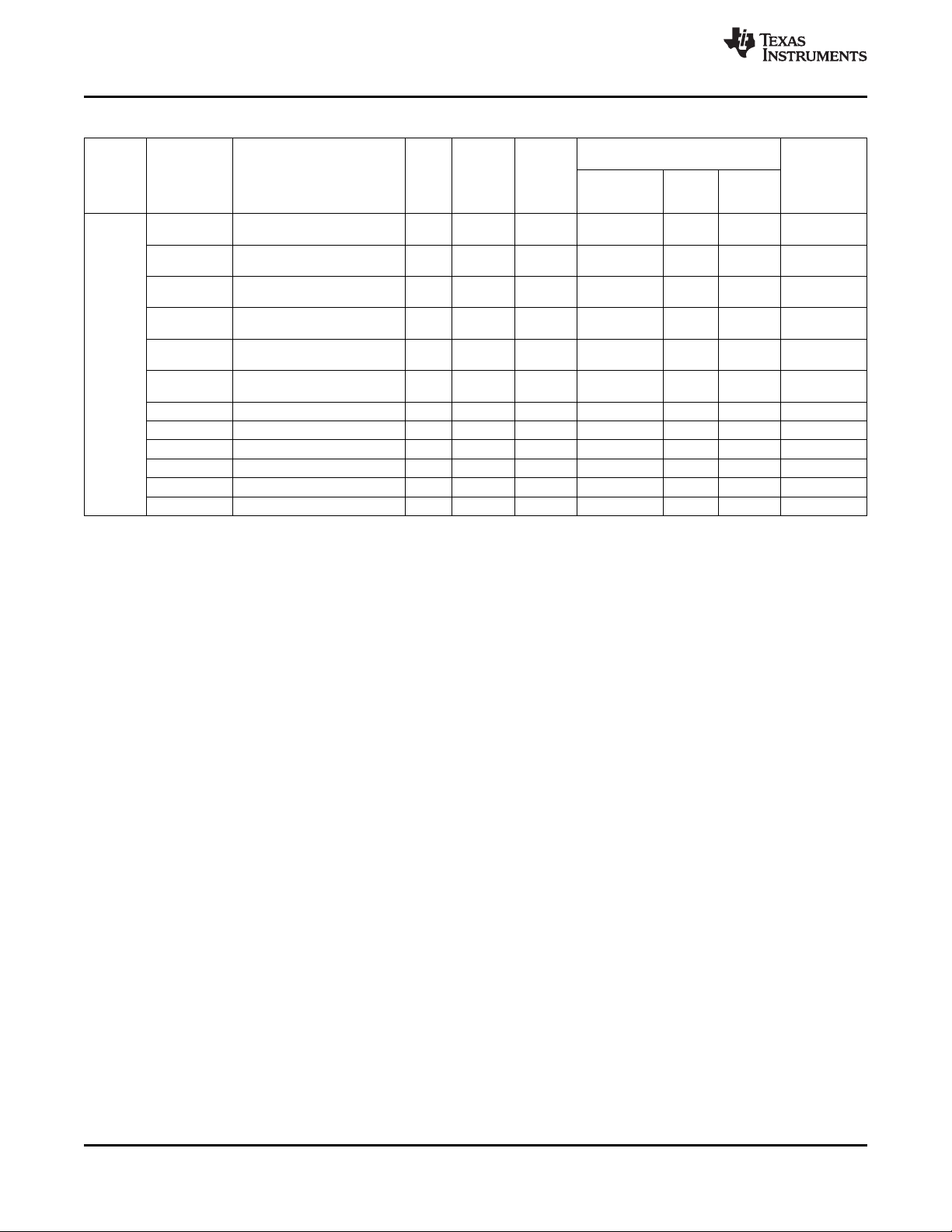
2.1 Ball Characteristics
Table 2-1 describes the terminal characteristics and the signals multiplexed on each pin. The following list
describes the table column headers:
1. Ball: Ball number(s) associated with each signal(s)
2. Pin Name: The names of all the signals that are multiplexed on each ball
3. A/D: Analog or digital signal
4. Type: The terminal type when a particular signal is multiplexed on the terminal:
– I = Input
– O = Output
5. Reference Level: See the power module chapter for values.
6. PU/PD: Denotes the presence of an internal pullup or pulldown. Pullups and pulldowns can be enabled
or disabled by software.
7. Buffer Strength: Drive strength of the associated output buffer
Table 2-1. Ball Characteristics
TPS65920 TPS65930 Pin A/D Reference Level
Ball[1] Ball[1] Name[2] [3] RL[5]
H2 H2 ADCIN0 A I/O VINTANA1.OUT
F2 F2 ADCIN2 A I VINTANA2.OUT
M5 M5 PCHGAC A I VACCHARGER
N1 N1 VPRECH A O VPRECH
N5 N5 VBAT A Power VBAT
F7 F7 75 100 202 59 100 144
GPIO0/CD1 D I/O IO_1P8 8
JTAG.TDO D I/O IO_1P8 8
Type[4] Strength
PU[6] (kΩ) PD[6] (kΩ) Buffer
Min Typ Max Min Typ Max
(mA)[7]
Copyright © 2008–2011, Texas Instruments Incorporated Terminal Description 13
Submit Documentation Feedback
focus.ti.com: TPS65930/TPS65920
TPS65930/TPS65920
SWCS037G–MAY 2008– REVISED APRIL 2011
Table 2-1. Ball Characteristics (continued)
TPS65920 TPS65930 Pin A/D Reference Level
Ball[1] Ball[1] Name[2] [3] RL[5]
E7 E7 75 100 202 59 100 144
P2 P2 156 220 450 59 100 144
P13 P13 156 220 450 59 100 144
L5 L5 PWM0 D O IO_1P8 75 100 202 59 100 144 4
J7 J7 75 100 202 59 100 144
D8 D8 SYSEN D Open drain/I IO_1P8 4.7 7.35 10 2
A4 A4 CLKEN D O IO_1P8 2
B13 B13 CLKREQ D I IO_1P8 60 100 146
C10 C10 INT1 D O IO_1P8 2
C8 C8 NRESPWRON D O IO_1P8 2
B9 B9 NRESWARM D I IO_1P8 2
D10 D10 PWRON D I VBAT
G5 G5 NSLEEP1 D I IO_1P8
E10 E10 CLK256FS
E4 E4 VMODE1 D I IO_1P8
E8 E8 BOOT0 A/D I/O VBAT
D7 D7 BOOT1 A/D I/O VBAT
B8 B8 REGEN D Open drain VBAT 5.5 8 12 2
H4 H4 MSECURE D I IO_1P8
L13 L13 VREF A Power VREF
K13 K13 AGND A ground GND
B3 B3
C5 C5
C3 C3 I2C.CNTL.SDA D I/O IO_1P8 2.5 3.4 12
B4 B4 I2C.CNTL.SCL D I IO_1P8 2.5 3.4 12
(2)
See
(2)
See
(2)
See
(2)
See
(2)
See
(2)
See
A10 A10 VBAT.RIGHT A Power VBAT
(2)
See
(2)
See
(2)
See
(2)
See
(2)
See
GPIO1 D I/O IO_1P8 2
JTAG.TMS D I IO_1P8
GPIO2 D I/O IO_1P8 2
TEST1 D I/O IO_1P8 2
GPIO15 D I/O IO_1P8 2
TEST2 D I/O IO_1P8 2
GPIO6 D I/O IO_1P8 2
TEST3 D I/O IO_1P8 2
GPIO7 D I/O IO_1P8 2
VIBRA.SYNC D I IO_1P8
PWM1 D O IO_1P8 4
TEST4 D I/O IO_1P8 2
(1)
N.C.
I2C.SR.SDA D I/O IO_1P8 2.5 3.4 12
VMODE2 D I IO_1P8 2
I2C.SR.SCL D I/O IO_1P8 2.5 3.4 12
H3 I2S.CLK D I/O IO_1P8 2
K2 I2S.SYNC D I/O IO_1P8 2
K4 I2S.DIN D I IO_1P8 2
K3 I2S.DOUT D O IO_1P8 2
D1 MIC.MAIN.P A I MICBIAS1.OUT
E1 MIC.MAIN.M A I MICBIAS1.OUT
PreDriv.LEFT A O VINTANA2.OUT
A7
VMID A Power VINTANA2.OUT
PreDriv.RIGHT A O VINTANA2.OUT
A8
ADCIN7 A I VINTANA2.OUT
G1 AUXR A I VINTANA2.OUT
MICBIAS1.OUT A Power VINTANA2.OUT
E2
VMIC1.OUT A Power VINTANA2.OUT
D2 MICBIAS.GND Power GND GND
Type[4] Strength
D O IO_1P8 2
Power
(GND)
PU[6] (kΩ) PD[6] (kΩ) Buffer
Min Typ Max Min Typ Max
www.ti.com
(mA)[7]
(1) To avoid reflection on this pin as a result of impedance mismatch, a serial resistance of 33 Ω must be added. This clock output is
available in TPS65920 also. Can be used as a clock source, if required.
(2) Balls A7, A8, D1, D2, E1, E2, G1, H3, K2, K3, and K4 are present on TPS65920 package. However, there is no function associated with
these pins. These can be left floating.
14 Terminal Description Copyright © 2008–2011, Texas Instruments Incorporated
Submit Documentation Feedback
focus.ti.com: TPS65930/TPS65920
TPS65930/TPS65920
www.ti.com
SWCS037G–MAY 2008– REVISED APRIL 2011
Table 2-1. Ball Characteristics (continued)
TPS65920 TPS65930 Pin A/D Reference Level
Ball[1] Ball[1] Name[2] [3] RL[5]
G2 G2 AVSS1 A Power GND GND
L7 L7 AVSS2 A Power GND GND
N14 N14 AVSS3 A Power GND GND
C7 C7 AVSS4 A Power GND GND
M10 M10 32KCLKOUT D O IO_1P8
L14 L14 32KXIN A I IO_1P8
K14 K14 32KXOUT A O IO_1P8
A11 A11 HFCLKIN A I IO_1P8
M11 M11 HFCLKOUT D O IO_1P8
P8 P8 VBUS A Power VBUS
N10 N10 DP/UART3.RXD A I/O VBUS 2
P10 P10 DN/UART3.TXD A I/O VBUS 2
G6 G6 ID A I/O VBUS 2
K11 K11 UCLK D I IO_1P8 16
H12 H12 75 100 202 59 100 144
H11 H11 75 100 202 59 100 144
J8 J8 75 100 202 59 100 144
L10 L10
K10 K10
G11 G11
G10 G10 UART4.CTSO D O IO_1P8 16
E12 E12 75 100 202 59 100 144
G9 G9 75 100 202 59 100 144
G12 G12 75 100 202 59 100 144
E11 E11 75 100 202 59 100 144
P14 P14 TEST.RESET A/D I VBAT 30 50 70
P1 P1 TESTV1 A I/O VBAT
A14 A14 TESTV2 A I/O VINTANA2.OUT
A1 A1 TEST D I IO_1P8 60 100 146
A13 A13 D I IO_1P8
B14 B14 D I IO_1P8
P7 P7 CP.IN A Power VBAT/VBUS
N7 N7 CP.CAPP A O CP.CAPP
N6 N6 CP.CAPM A O CP.CAPM
P5 P5 CP.GND A Power GND GND
N9 N9 VBAT.USB A Power VBAT
M8 M8 VUSB.3P1 A Power VUSB.3P1
L1 L1 VAUX12S.IN A Power VBAT
N2 N2 VAUX2.OUT A Power VAUX2.OUT
H14 H14 VPLLA3R.IN A Power VBAT
K12 K12 VRTC.OUT A Power VRTC.OUT
STP D I IO_1P8 16
GPIO9 D I/O IO_1P8 2
DIR D O IO_1P8 16
GPIO10 D I/O IO_1P8 2
NXT D O IO_1P8 16
GPIO11 D I/O IO_1P8 2
DATA0 D I/O IO_1P8 16
UART4.TXD D I IO_1P8
DATA1 D I/O IO_1P8 16
UART4.RXD D O IO_1P8 2
DATA2 D I/O IO_1P8 16
UART4.RTSI D I IO_1P8
DATA3 D I/O IO_1P8 16
GPIO12 D I/O IO_1P8 75 100 202 59 100 144 16
DATA4 D I/O IO_1P8 16
GPIO14 D I/O IO_1P8 2
DATA5 D I/O IO_1P8 16
GPIO3 D I/O IO_1P8 2
DATA6 D I/O IO_1P8 16
GPIO4 D I/O IO_1P8 2
DATA7 D I/O IO_1P8 16
GPIO5 D I/O IO_1P8 2
JTAG.TDI/
BERDATA
JTAG.TCK/
BERCLK
Type[4] Strength
PU[6] (kΩ) PD[6] (kΩ) Buffer
Min Typ Max Min Typ Max
60 100 140 60 100 140
(mA)[7]
Copyright © 2008–2011, Texas Instruments Incorporated Terminal Description 15
Submit Documentation Feedback
focus.ti.com: TPS65930/TPS65920

TPS65930/TPS65920
SWCS037G–MAY 2008– REVISED APRIL 2011
Table 2-1. Ball Characteristics (continued)
TPS65920 TPS65930 Pin A/D Reference Level
Ball[1] Ball[1] Name[2] [3] RL[5]
G14 G14 VPLL1.OUT A Power VPLL1.OUT
A2 A2 VMMC1.IN A Power VBAT
B1 B1 VMMC1.OUT A Power VMMC1.OUT
M7 M7 A Power VINTUSB1P5.OUT
N8 N8 A Power VINTUSB1P8.OUT
K1 K1 VDAC.IN A Power VBAT
L2 L2 VDAC.OUT A Power VDAC.OUT
H13 H13 VINT.IN A Power VBAT
H1 H1 VINTANA1.OUT A Power VINTANA1.OUT
J2 J2 VINTANA2.OUT A Power VINTANA2.OUT
A5 A5 VINTANA2.OUT A Power VINTANA2.OUT
J13 J13 VINTDIG.OUT A Power VINTDIG.OUT
D13 D13 VDD1.IN A Power VBAT
D12 D12 VDD1.IN A Power VBAT
D14 D14 VDD1.IN A Power VBAT
C11 C11 VDD1.SW A O VBAT
C12 C12 VDD1.SW A O VBAT
C13 C13 VDD1.SW A O VBAT
E14 E14 VDD1.FB A I
A12 A12 VDD1.GND A Power GND GND
B11 B11 VDD1.GND A Power GND GND
B12 B12 VDD1.GND A Power GND GND
M13 M13 VDD2.IN A Power VBAT
M12 M12 VDD2.IN A Power VBAT
N13 N13 VDD2.FB A I
N11 N11 VDD2.SW A O VBAT
P11 P11 VDD2.SW A O VBAT
N12 N12 VDD2.GND A Power GND GND
P12 P12 VDD2.GND A Power GND GND
M2 M2 VIO.IN A Power VBAT
M3 M3 VIO.IN A Power VBAT
M4 M4 VIO.FB A I
N4 N4 VIO.SW A O VBAT
P4 P4 VIO.SW A O VBAT
N3 N3 VIO.GND A Power GND GND
P3 P3 VIO.GND A Power GND GND
H9 H9 BKBAT A Power VBACK
B7 B7 IO.1P8 A Power IO_1P8
H10 H10 DGND A Power GND GND
F13 F13 LEDGND A Power GND GND
B10 B10 75 100 202 59 100 144
E13 E13
G13 G13
G4 G4 KPD.C0 D Open drain IO_1P8
G3 G3 KPD.C1 D Open drain IO_1P8
E5 E5 KPD.C2 D Open drain IO_1P8
B2 B2 KPD.C3 D Open drain IO_1P8
E3 E3 KPD.C4 D Open drain IO_1P8
D5 D5 KPD.C5 D Open drain IO_1P8
K7 K7 KPD.R0 D I IO_1P8 8 10 12
VINTUSB1P5.
OUT
VINTUSB1P8.
OUT
GPIO13 D I/O IO_1P8
LEDSYNC D I IO_1P8
LEDA A Open drain VBAT
VIBRA.P A Open drain VBAT
LEDB A Open drain VBAT
VIBRA.M A Open drain VBAT
Type[4] Strength
PU[6] (kΩ) PD[6] (kΩ) Buffer
Min Typ Max Min Typ Max
www.ti.com
(mA)[7]
16 Terminal Description Copyright © 2008–2011, Texas Instruments Incorporated
Submit Documentation Feedback
focus.ti.com: TPS65930/TPS65920
TPS65930/TPS65920
www.ti.com
Table 2-1. Ball Characteristics (continued)
TPS65920 TPS65930 Pin A/D Reference Level
Ball[1] Ball[1] Name[2] [3] RL[5]
H5 H5 KPD.R1 D I IO_1P8 8 10 12
K5 K5 KPD.R2 D I IO_1P8 8 10 12
H6 H6 KPD.R3 D I IO_1P8 8 10 12
K8 K8 KPD.R4 D I IO_1P8 8 10 12
L8 L8 KPD.R5 D I IO_1P8 8 10 12
Type[4] Strength
PU[6] (kΩ) PD[6] (kΩ) Buffer
Min Typ Max Min Typ Max
2.2 Signal Description
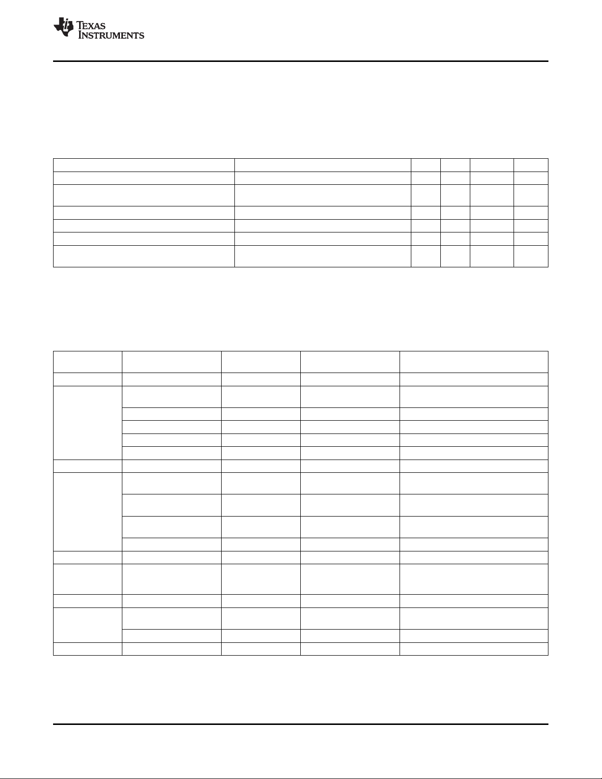
Table 2-2 describes the signals on the TPS65920 and TPS65930 devices; some signals are available on
multiple pins.
Table 2-2. Signal Description
Module Description Type
ADC
Charger
GPIOs/ TEST2 I/O
JTAG
Signal TPS65920 TPS65930 Features
Name Ball Ball Not Used
ADCIN0 Battery type I/O H2 H2 ADCIN0 GND
ADCIN2 General-purpose ADC input I F2 F2 ADCIN2 I GND
PCHGAC I M5 M5 PCHGAC I GND
VPRECH Precharge regulator output O N1 N1 VPRECH O Cap to GND
VBAT Battery voltage sensing Power N5 N5 VBAT Power VBAT
GPIO0/CD1 GPIO0/card detection 1 I/O
JTAG.TDO JTAG test data output I/O
GPIO1 GPIO1 I/O
JTAG.TMS JTAG test mode state I
GPIO2 GPIO2 I/O
TEST1 I/O
GPIO15 GPIO15 I/O
GPIO6 GPIO6 I/O
PWM0 Pulse width driver 0 O
TEST3 I/O
GPIO7 GPIO7 I/O
VIBRA.SYNC Vibrator on-off synchronization I
PWM1 Pulse width driver O
TEST4 I/O
AC precharge sense signal. Also
used for EEPROM.
TEST1 pin used in test mode
only
TEST2 pin used in test mode
only
TEST3 pin used in test mode
only (controlled by JTAG)
TEST4 pin used in test mode
only (controlled by JTAG)
F7 F7 GPIO0 I PD Floating
E7 E7 GPIO1 I PD Floating
P2 P2 GPIO2 I PD Floating
P13 P13 GPIO15 I PD Floating
L5 L5 GPIO6 I PD Floating
J7 J7 GPIO7 I PD Floating
SWCS037G–MAY 2008– REVISED APRIL 2011
Default Configuration After Reset
Released
Internal
Signal Type Pull or
Not
(mA)[7]
(1)
(2)
Copyright © 2008–2011, Texas Instruments Incorporated Terminal Description 17
Submit Documentation Feedback
focus.ti.com: TPS65930/TPS65920
TPS65930/TPS65920
SWCS037G–MAY 2008– REVISED APRIL 2011
www.ti.com
Table 2-2. Signal Description (continued)
Default Configuration After Reset
Module Description Type
CONTROL
VREF
I2C
Smart
Reflex
I2C
TDM
ANA.MIC
HandsFree
Headset
AUX Input AUXR Auxiliary audio input right I G1 AUXR I Cap to GND
Signal TPS65920 TPS65930 Features
Name Ball Ball Not Used
SYSEN System enable output D8 D8 SYSEN OD PU Floating
CLKEN Clock enable O A4 A4 CLKEN O Floating
CLKREQ Clock request I B13 B13 CLKREQ I PD GND
INT1 Output interrupt line 1 O C10 C10 INT1 O Floating
NRESPWRON O C8 C8 NRESPWRON O Floating
NRESWARM I B9 B9 NRESWARM I GND
PWRON I D10 D10 PWRON I VBAT
NSLEEP1 Sleep request from device 1 I G5 G5 NSLEEP1 I GND
CLK256FS O E10 E10 CLK256FS O Floating
VMODE1 I E4 E4 VMODE1 I GND
BOOT0 Boot pin 0 I E8 E8 BOOT0 I PD N/A
BOOT1 Boot pin 1 I D7 D7 BOOT1 I PD N/A
REGEN Enable signal for external LDO B8 B8 REGEN OD PU Floating
MSECURE I H4 H4 MSECURE I N/A
VREF Reference voltage Power L13 L13 VREF Power N/A
AGND K13 K13 AGND GND
N.C. Not connected
I2C.SR.SDA I/O
VMODE2 I
I2C.SR.SCL I/O
I2C.CNTL.SDA I/O C3 C3 I2C.CNTL.SDA I/O PU N/A
I2C.CNTL.SCL I/O B4 B4 I2C.CNTL.SCL I/O PU N/A
I2S.CLK Clock signal (audio port) I/O H3 I2S.CLK I/O Floating
I2S.SYNC I/O K2 I2S.SYNC I/O Floating
I2S.DIN Data receive (audio port) I K4 I2S.DIN I GND
I2S.DOUT Data transmit (audio port) O K3 I2S.DOUT O Floating
MIC.MAIN.P Main microphone left input (P) I D1 MIC.MAIN.P I Cap to GND
MIC.MAIN.M Main microphone left input (M) I E1 MIC.MAIN.M I Cap to GND
VBAT.RIGHT Battery voltage input Power A10 A10 VBAT.RIGHT Power VBAT
PreDriv.LEFT O
VMID Power
PreDriv.RIGHT O
ADCIN7 General-purpose ADC input 7 I
Output control the NRESPWRON
of the application processor
Input; detect user action on the
reset button
Input; detect a control command
to start or stop the system
Digital voltage scaling linked with
VDD1
Security and digital rights
management
Analog ground for reference Power Power
voltage GND GND
SmartReflex I2C data
Digital voltage scaling linked with
VDD2
SmartReflex I2C data
General-purpose I2C data
General-purpose I2C clock
Synchronization signal (audio
port)
Predriver output left P for
external class-D amplifier
Predriver output right P for
external class-D amplifier
Open
drain/I
Open
drain
B3 B3 Floating
C5 C5 VMODE2 I GND
A7 VMID Power Floating
A8 ADCIN7 I GND
Signal Type Pull or
Signal not
functional
Released
Internal
Not
(3)
(1)
18 Terminal Description Copyright © 2008–2011, Texas Instruments Incorporated
Submit Documentation Feedback
focus.ti.com: TPS65930/TPS65920
TPS65930/TPS65920
www.ti.com
SWCS037G–MAY 2008– REVISED APRIL 2011
Table 2-2. Signal Description (continued)
Default Configuration After Reset
Module Description Type
VMIC
BIAS
CLOCK 32KXOUT Output of the 32-kHz oscillator O K14 K14 32KXOUT O Floating
USB PHY
ULPI G11 G11 DATA2 O Floating
Signal TPS65920 TPS65930 Features
Name Ball Ball Not Used
MICBIAS1.
OUT
VMIC1.OUT Power
MICBIAS.GND D2 MICBIAS.GND GND
AVSS1 G2 G2 AVSS1
AVSS2 L7 L7 AVSS2
AVSS3 N14 N14 AVSS3
AVSS4 C7 C7 AVSS4
32KCLKOUT O M10 M10 32KCLKOUT O Floating
32KXIN Input of the 32-kHz oscillator I L14 L14 32KXIN I N/A
HFCLKIN I A11 A11 HFCLKIN I N/A
HFCLKOUT HS clock output O M11 M11 HFCLKOUT O Floating
VBUS VBUS power rail Power P8 P8 VBUS Power N/A
DP/ data/universal asynchronous DP/UART3.RX
UART3.RXD receiver/transmitter (UART)3 D
DN/ USB data N/USB carkit transmit DN/UART3.TX
UART3.TXD data/UART3 transmit data D
ID USB ID I/O G6 G6 ID I/O
UCLK HS USB clock I K11 K11 UCLK O Floating
STP HS USB stop I
GPIO9 GPIO9 I/O
DIR HS USB direction O
GPIO10 GPIO10 I/O
NXT HS USB next O
GPIO11 GPIO11 I/O
DATA0 HS USB Data0 I/O
UART4.TXD UART4.TXD I
DATA1 HS USB Data1 I/O
UART4.RXD UART4.RXD O
DATA2 HS USB Data2 I/O
UART4.RTSI UART4.RTSI I
DATA3 HS USB Data3 I/O
UART4.CTSO UART4.CTSO O G10 G10 DATA3 O Floating
GPIO12 GPIO12 I/O
DATA4 HS USB Data4 I/O
GPIO14 GPIO14 I/O
DATA5 HS USB Data5 I/O
GPIO3 GPIO3 I/O
DATA6 HS USB Data6 I/O
GPIO4 GPIO4 I/O
DATA7 HS USB Data7 I/O
GPIO5 GPIO5 I/O
Analog microphone bias 1 Power
Digital microphone power supply
1
Dedicated ground for Power Power
microphones GND GND
Analog ground GND
Buffered output of the 32-kHz
digital clock
Input of the digital (or sine) HS
clock
USB data P/USB carkit receive
receive data
Power Power
GND GND
I/O N10 N10 I/O N/A
I/O P10 P10 I/O N/A
H12 H12 STP I PU Floating
H11 H11 DIR O Floating
J8 J8 NXT O Floating
L10 L10 DATA0 O Floating
K10 K10 DATA1 O Floating
E12 E12 DATA4 O Floating
G9 G9 DATA5 O Floating
G12 G12 DATA6 O Floating
E11 E11 DATA7 O Floating
E2 MICBIAS1.OUT Power Floating
Signal Type Pull or
Released
Internal
Not
Connected to
VRUSB3V1
(1)
Copyright © 2008–2011, Texas Instruments Incorporated Terminal Description 19
Submit Documentation Feedback
focus.ti.com: TPS65930/TPS65920
TPS65930/TPS65920
SWCS037G–MAY 2008– REVISED APRIL 2011
www.ti.com
Table 2-2. Signal Description (continued)
Default Configuration After Reset
Module Description Type
TEST
USB CP
VBAT.US USB LDOs (VINTUSB1P5,
B VINTUSB1P8, VUSB.3P1) VBAT
USB.LDO VUSB.3P1 USB LDO output Power M8 M8 VUSB.3P1 Power N/A
VAUX1 VAUX12S.IN Power L1 L1 VAUX12S.IN Power VBAT
VAUX2 VAUX2.OUT VAUX2 LDO output voltage Power N2 N2 VAUX2.OUT Power Floating
VPLLA3R VPLLA3R.IN Power H14 H14 VPLLA3R.IN Power VBAT
VRTC VRTC.OUT Power K12 K12 VRTC.OUT Power N/A
VPLL1 VPLL1.OUT LDO output voltage Power G14 G14 VPLL1.OUT Power Floating
VMMC1
VINTUSB1 VINTUSB1P5. VINTUSB1P5 internal LDO VINTUSB1P5.
P5 OUT output (internal use only) OUT
VINTUSB1 VINTUSB1P8. VINTUSB1P8 internal LDO VINTUSB1P8.
P8 OUT output (internal use only) OUT
Video
DAC
VINT VINT.IN Input for VINTDIG LDO Power H13 H13 VINT.IN Power VBAT
VINTANA1 Power H1 H1 Power N/A
VINTANA2
VINTDIG VINTDIG.OUT Power J13 J13 VINTDIG.OUT Power N/A
Signal TPS65920 TPS65930 Features
Name Ball Ball Not Used
TEST.RESET I P14 P14 TEST.RESET I PD GND
TESTV1 Analog test I/O P1 P1 TESTV1 I/O Floating
TESTV2 Analog test I/O A14 A14 TESTV2 I/O Floating
TEST and application mode for I A1 A1 TEST I PD Floating
JTAG.TDI/ JTAG.TDI/
BERDATA BERDATA
JTAG.TCK/ JTAG.TCK/
BERCLK BERCLK
CP.IN Charge pump input voltage Power P7 P7 CP.IN Power VBAT
CP.CAPP Charge pump flying capacitor P O N7 N7 CP.CAPP O Floating
CP.CAPM Charge pump flying capacitor M O N6 N6 CP.CAPM O Floating
CP.GND Charge pump ground P5 P5 CP.GND GND
VBAT.USB Power N9 N9 VBAT.USB Power VBAT
VMMC1.IN VMMC1 LDO input voltage Power A2 A2 VMMC1.IN Power VBAT
VMMC1.OUT VMMC1 LDO output voltage Power B1 B1 VMMC1.OUT Power Floating
VDAC.IN Power K1 K1 VDAC.IN Power VBAT
VDAC.OUT Output voltage of the regulator Power L2 L2 VDAC.OUT Power Floating
VINTANA1. VINTANA1 internal LDO output VINTANA1.OU
OUT (internal use only) T
VINTANA2. VINTANA2 internal LDO output VINTANA2.OU
OUT (internal use only) T
VINTANA2. VINTANA2 internal LDO output VINTANA2.OU
OUT (internal use only) T
Reset T2 device (except power
state-machine)
Selection between JTAG mode
JTAG/GPIOs (with PU or PD)
JTAG.TDI/BERDATA I A13 A13 I GND
JTAG.TCK/BERCLK I B14 B14 I GND
Power Power
GND GND
VAUX1/VAUX2/VSIM LDO input
voltage
Input for VPLL1, VPLL2, VAUX3,
and VRTC LDOs
VRTC internal LDO output
(internal use only)
Power M7 M7 Power Floating
Power N8 N8 Power Floating
Input for VDAC, VINTANA1, and
VINTANA2 LDOs
Power J2 J2 Power N/A
Power A5 A5 Power N/A
VINTDIG internal LDO output
(internal use only)
Signal Type Pull or
Released
Internal
Not
(1)
20 Terminal Description Copyright © 2008–2011, Texas Instruments Incorporated
Submit Documentation Feedback
focus.ti.com: TPS65930/TPS65920
TPS65930/TPS65920
www.ti.com
SWCS037G–MAY 2008– REVISED APRIL 2011
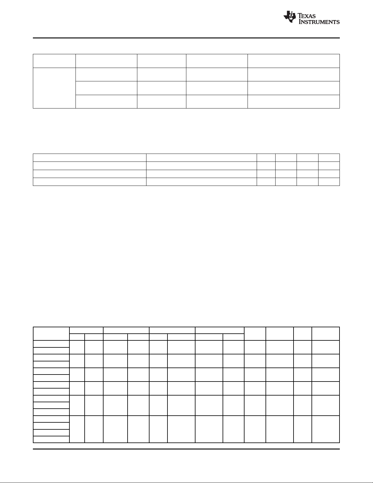
Table 2-2. Signal Description (continued)
Default Configuration After Reset
Module Description Type
VDD1
VDD2
VIO
Backup
battery
Digital TPS65920/TPS65930 device I/O
VDD input
Digital Power Power
ground GND GND
LED driver
Signal TPS65920 TPS65930 Features
Name Ball Ball Not Used
VDD1.IN VDD1 dc-dc input voltage Power D13 D13 VDD1.IN Power VBAT
VDD1.IN VDD1 dc-dc input voltage Power D12 D12 VDD1.IN Power VBAT
VDD1.IN VDD1 dc-dc input voltage Power D14 D14 VDD1.IN Power VBAT
VDD1.SW VDD1 dc-dc switch O C11 C11 VDD1.SW O Floating
VDD1.SW VDD1 dc-dc switch O C12 C12 VDD1.SW O Floating
VDD1.SW VDD1 dc-dc switch O C13 C13 VDD1.SW O Floating
VDD1.FB I E14 E14 VDD1.FB I GND
VDD1.GND VDD1 dc-dc ground A12 A12 VDD1.GND GND
VDD1.GND VDD1 dc-dc ground B11 B11 VDD1.GND GND
VDD1.GND VDD1 dc-dc ground B12 B12 VDD1.GND GND
VDD2.IN VDD2 dc-dc input voltage Power M13 M13 VDD2.IN Power VBAT
VDD2.IN VDD2 dc-dc input voltage Power M12 M12 VDD2.IN Power VBAT
VDD2.FB I N13 N13 VDD2.FB I GND
VDD2.SW VDD2 dc-dc switch O N11 N11 VDD2.SW O Floating
VDD2.SW VDD2 dc-dc switch O P11 P11 VDD2.SW O Floating
VDD2.GND VDD2 dc-dc ground N12 N12 VDD2.GND GND
VDD2.GND VDD2 dc-dc ground P12 P12 VDD2.GND GND
VIO.IN VIO dc-dc input voltage Power M2 M2 VIO.IN Power VBAT
VIO.IN VIO dc-dc input voltage Power M3 M3 VIO.IN Power VBAT
VIO.FB I M4 M4 VIO.FB I GND
VIO.SW VIO dc-dc switch O N4 N4 VIO.SW O Floating
VIO.SW VIO dc-dc switch O P4 P4 VIO.SW O Floating
VIO.GND VIO dc-dc ground N3 N3 VIO.GND GND
VIO.GND VIO dc-dc ground P3 P3 VIO.GND GND
BKBAT Backup battery Power H9 H9 BKBAT Power GND
IO.1P8 Power B7 B7 IO.1P8 Power N/A
DGND Digital ground H10 H10 DGND GND
LEDGND LED driver ground F13 F13 LEDGND GND
GPIO13 GPIO13 I/O
LEDSYNC LED synchronization input I
LEDA LED leg A
VIBRA.P H-bridge vibrator P
LEDB LED leg B
VIBRA.M H-bridge vibrator M
VDD1 dc-dc output voltage
(feedback)
VDD2 dc-dc output voltage
(feedback)
VIO dc-dc output voltage
(feedback)
Power Power
GND GND
Power Power
GND GND
Power Power
GND GND
Power Power
GND GND
Power Power
GND GND
Power Power
GND GND
Power Power
GND GND
Power Power
GND GND
B10 B10 GPIO13 I PD Floating
Open Signal not
drain functional
Open Signal not
drain functional
E13 E13 Floating
G13 G13 Floating
Signal Type Pull or
Released
(3)
(3)
Internal
Not
(1)
Copyright © 2008–2011, Texas Instruments Incorporated Terminal Description 21
Submit Documentation Feedback
focus.ti.com: TPS65930/TPS65920
TPS65930/TPS65920
SWCS037G–MAY 2008– REVISED APRIL 2011
www.ti.com
Table 2-2. Signal Description (continued)
Default Configuration After Reset
Module Description Type
Keypad
Signal TPS65920 TPS65930 Features
Name Ball Ball Not Used
KPD.C0 Keypad column 0 G4 G4 KPD.C0 OD Floating
KPD.C1 Keypad column 1 G3 G3 KPD.C1 OD Floating
KPD.C2 Keypad column 2 E5 E5 KPD.C2 OD Floating
KPD.C3 Keypad column 3 B2 B2 KPD.C3 OD Floating
KPD.C4 Keypad column 4 E3 E3 KPD.C4 OD Floating
KPD.C5 Keypad column 5 D5 D5 KPD.C5 OD Floating
KPD.R0 Keypad row 0 I K7 K7 KPD.R0 I PU Floating
KPD.R1 Keypad row 1 I H5 H5 KPD.R1 I PU Floating
KPD.R2 Keypad row 2 I K5 K5 KPD.R2 I PU Floating
KPD.R3 Keypad row 3 I H6 H6 KPD.R3 I PU Floating
KPD.R4 Keypad row 4 I K8 K8 KPD.R4 I PU Floating
KPD.R5 Keypad row 5 I L8 L8 KPD.R5 I PU Floating
Open
drain
Open
drain
Open
drain
Open
drain
Open
drain
Open
drain
Signal Type Pull or
(1) This column provides the connection when the associated feature is not used or not connected. When there is a pin muxing, not all
functions on the muxed pin are used. But even if a function is not used, the Default Configuration After Reset Released column still
applies.
Connection criteria:
– Analog pins:
– For input: GND
– For output: Floating (except VPRECH is connected to GND)
– For I/O if input by default: GND (except for audio features input: capacitor to ground with a 100-nF typical value capacitor)
– Digital pins:
– For input: GND (except keypad and STP are left floating)
– For input and pullup: Floating
– For output: Floating
– For I/O and pullup: Floating
N/A (not applicable): When the associated feature is mandatory for correct functioning of the TPS65920/TPS65930 device
(2) The signal VPRECH must be connected to the CPRECH capacitor to GND.
(3) Signal not functional indicates that no signal is presented on the pad after a release reset.
Released
Internal
Not
(1)
22 Terminal Description Copyright © 2008–2011, Texas Instruments Incorporated
Submit Documentation Feedback
focus.ti.com: TPS65930/TPS65920
TPS65930/TPS65920
www.ti.com
SWCS037G–MAY 2008– REVISED APRIL 2011
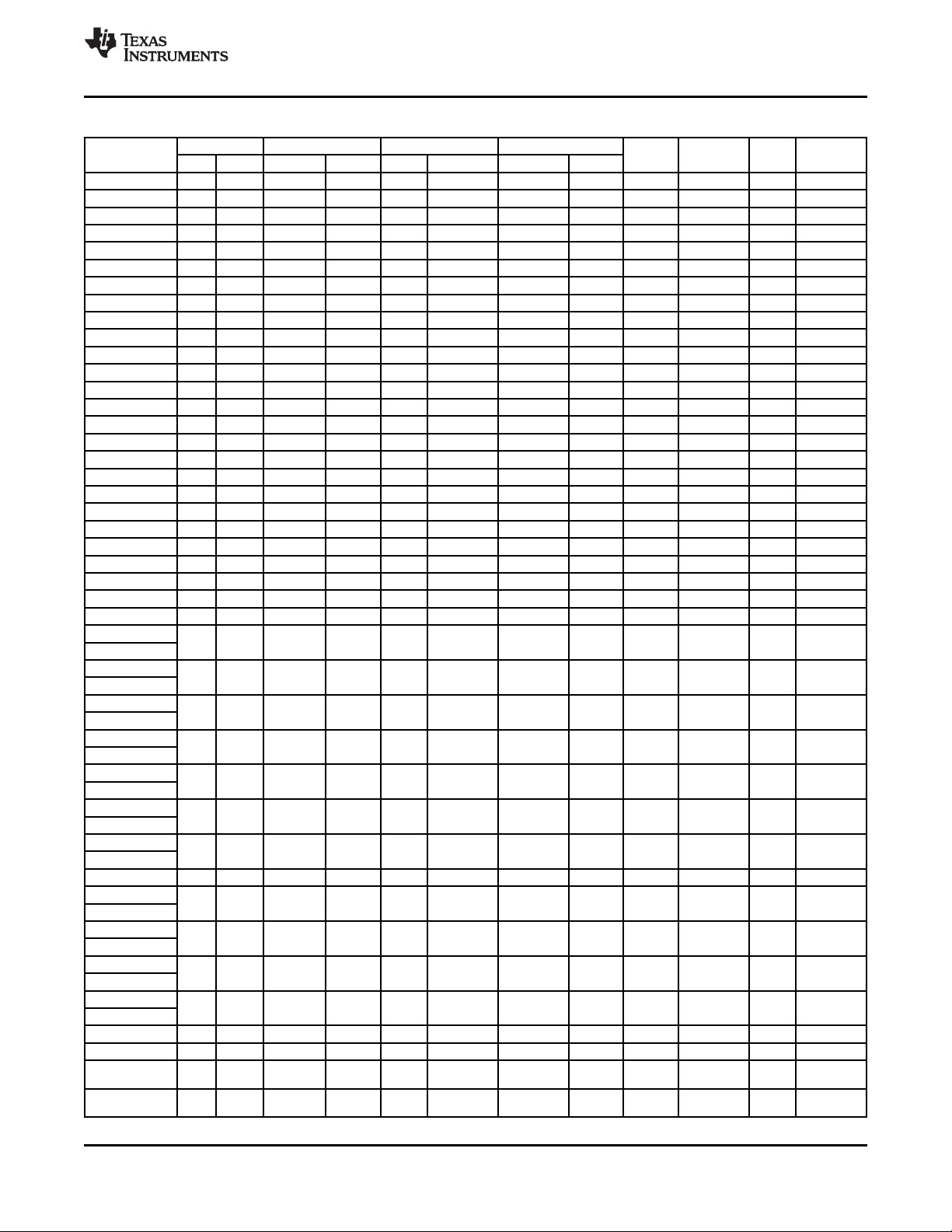
3 Electrical Characteristics
3.1 Absolute Maximum Ratings
Table 3-1 lists the absolute maximum ratings.
Table 3-1. Absolute Maximum Ratings
Parameter Test Conditions Min Typ Max Unit
Main battery supply voltage
Voltage on any input Supply represents the voltage applied to the 0.0 1.0*Supply V
Storage temperature range –55 125 °C
Ambient temperature range –40 85 °C
Junction temperature (TJ) At 1.4 W (Theta JB 11°C/W 2S2P board) 105 °C
Junction temperature (TJ) for parametric –40 105 °C
compliance
(1) The product has negligible reliability impact if voltage spikes of 5.2 V occur for a total duration of 10 milliseconds.
3.2 Minimum Voltages and Associated Currents
Table 3-2 lists the VBAT minimum and maximum currents per VBAT ball.
Table 3-2. VBAT Minimum Required Per VBAT Ball and Associated Maximum Current
(1)
power supply pin associated with the input
2.1 4.5 V
Category Pin and Module Maximum Current Output Voltage (V) VBAT Minimum (V)
VBAT pin name VDD_VPLLA3R_IN_6POV 340
VPLL1 (LDO) 40 1.0 / 1.2 / 1.3 / 1.8 / 2.8 / Maximum
Internal module
supplied VDD2 core (DCDC) < 1 2.7
VBAT pin name VDD_VDAC_IN_6POV 370
Internal module
supplied
VBAT pin name VDD_VAUXI2S_IN_6POV 350
Internal module
supplied
VBAT pin name VDD_VMMC1_IN_6POV 220
Internal module VMMC1 (LDO) 220 1.85 / 2.85 / 3.0 / 3.15 Maximum
supplied (2.7, output voltage selected + 250 mV)
VBAT pin name VDD_VINT_IN_6POV 131
VDD1 core (DCDC) < 1 2.7
SYSPOR (power ref) < 1 2.7
PBIAS (power ref) < 1 2.7
VDAC (LDO) 70 1.2 / 1.3 / 1.8 Maximum
VINTANA1 (LDO) 50 1.5 Maximum
VINTANA2 (LDO) 250 2.5 / 2.75 Maximum
VIO core (DCDC) < 1 2.7
VAUX2 (LDO) 100 1.3 / 1.5 / 1.6 / 1.7 / 1.8 / Maximum
Power_REGBATT 0.001 2.7
Specified (mA)
3.0 (2.7, output voltage selected + 250 mV)
(2.7, output voltage selected + 250 mV)
(2.7, output voltage selected + 250 mV)
(2.7, output voltage selected +250 mV)
1.9 / 2.0 / 2.1 / 2.2 / 2.3 / (2.7, output voltage selected + 250 mV)
2.4 / 2.5 / 2.8
Copyright © 2008–2011, Texas Instruments Incorporated Electrical Characteristics 23
Submit Documentation Feedback
focus.ti.com: TPS65930/TPS65920
TPS65930/TPS65920
SWCS037G–MAY 2008– REVISED APRIL 2011
www.ti.com
Table 3-2. VBAT Minimum Required Per VBAT Ball and Associated Maximum Current (continued)
Category Pin and Module Maximum Current Output Voltage (V) VBAT Minimum (V)
VINTDIG (LDO) 80 1.0 / 1.2 / 1.3 / 1.5 Maximum
Internal module VRRTC (LDO) 30 1.5 Maximum
supplied (2.7, output voltage selected + 250 mV)
VBACKUP (LDO) 1 2.5 / 3.0 / 3.1 / 3.2 Maximum
Specified (mA)
(2.7, output voltage selected + 250 mV)
(2.7, output voltage selected + 250 mV)
3.3 Recommended Operating Conditions
Table 3-3 lists the recommended operating maximum ratings.
Table 3-3. Recommended Operating Maximum Ratings
Parameter Test Conditions Min Typ Max Unit
Main battery supply voltage 2.7
Backup battery supply voltage 1.8 3.2 3.3 V
Ambient temperature range –40 85 °C
(1) 2.7 V is the minimum threshold for the battery at which the device will turn OFF. However, the minimum voltage at which the device will
power ON is 3.2 V ±100 mV (if PWRON does not have a switch and is connected to VBAT) considering battery plug as the device
switch on event. If PWRON has a switch then 3.2 V is the minimum for the device to turn ON.
(1)
3.6 4.5 V
3.4 Digital I/O Electrical Characteristics
Table 3-4 describes the digital I/O electrical characteristics. The following list defines abbreviations used in
the table:
• RL: Reference level voltage applied to the I/O cell
• VOL: Low-level output voltage
• VOH: High-level output voltage
• VIL: Low-level input voltage
• VIH: High-level input voltage
• Min: Minimum value
• Max: Maximum value
Table 3-4. Digital I/O Electrical Characteristics
Pin Name Fall Time (ns)
GPIO0/CD1
JTAG.TDO
GPIO0
JTAG.TMS
GPIO2
TEST1
GPIO15
TEST2
GPIO6
PWM0 0 0.45 RL–0.45 RL 0 0.35xRL 0.65xRL RL 3 30 5.2 5.2
TEST3
GPIO7
VIBRA.SYNC
PWM1
TEST4
VOL (V) VOH (V) VIL (V) VIL (V)
Min Max Min Max Min Max Min Max
0 0.45 RL–0.45 RL 0 0.35xRL 0.65xRL RL 33 30 5.2 5.2
0 0.45 RL–0.45 RL 0 0.35xRL 0.65xRL RL 33 30 5.2 5.2
0 0.45 RL–0.45 RL 0 0.35xRL 0.65xRL RL 3 30 5.2 5.2
0 0.45 RL–0.45 RL 0 0.35xRL 0.65xRL RL 3 30 5.2 5.2
0 0.45 RL–0.45 RL 0 0.35xRL 0.65xRL RL 3 30 5.2 5.2
Max Freq Load (pF) Rise
(MHz) Output Mode Time (ns)
24 Electrical Characteristics Copyright © 2008–2011, Texas Instruments Incorporated
Submit Documentation Feedback
focus.ti.com: TPS65930/TPS65920
TPS65930/TPS65920
www.ti.com
SWCS037G–MAY 2008– REVISED APRIL 2011
Table 3-4. Digital I/O Electrical Characteristics (continued)
Pin Name Fall Time (ns)
SYSEN 0 0.45 RL–0.45 RL 0 0.35×RL 0.65×RL RL 5.2 5.2
CLKEN 0 0.45 RL–0.45 RL 0 0.35×RL 0.65×RL RL 3 30 33.3 33.3
CLKREQ 0 0.45 RL–0.45 RL 0 0.35×RL 0.65×RL RL 3 33.3 33.3
INT1 0 0.45 RL–0.45 RL 0 0.35×RL 0.65×RL RL 3 30 33.3 33.3
NRESPWRON 0 0.45 RL–0.45 RL 0 0.35×RL 0.65×RL RL 3 30 33.3 33.3
NRESWARM 0 0.45 RL–0.45 RL 0 0.35×RL 0.65×RL RL 3 30 33.3 33.3
PWRON 0 0.35×1.8V 0.65×1.8V VBAT 3 33.3 33.3
NSLEEP1 0 0.45 RL–0.45 RL 0 0.35×RL 0.65×RL RL 3 33.3 33.3
CLK256FS 0 0.45 RL–0.45 RL 0 0.35×RL 0.65×RL RL 12.288 30 16.3 16.3
VMODE1 0 0.45 RL–0.45 RL 0 0.35×RL 0.65×RL RL 3 33.3 33.3
BOOT0 0 RL 3 33.3 33.3
BOOT1 0 RL 3 33.3 33.3
REGEN 0 0.45 RL–0.45 RL 0 0.35×RL 0.65×RL RL 3 30 33.3 33.3
MSECURE 0 0.45 RL–0.45 RL 0 0.35×RL 0.65×RL RL 3 33.3 33.3
I2C.SR.SDA 0 0.4 –0.5 0.3×RL 0.7×RL RL+0.5 3.4 Up to 400
VMODE2 0 0.45 RL–0.45 RL 0 0.35×RL 0.65×RL RL 3.4 29.4 29.4
I2C.SR.SCL 0 0.4 –0.5 0.3×RL 0.7×RL RL+0.5 3.4 10.0 10.0
I2C.CNTL.SDA 0 0.4 –0.5 0.3×RL 0.7×RL RL+0.5 3.4 Up to 400
I2C.CNTL.SCL 0 0.4 –0.5 0.3×RL 0.7×RL RL+0.5 3.4 10.0 10.0
I2S.CLK 0 0.45 RL–0.45 RL 0 0.35×RL 0.65×RL RL 6.5 30 33.0 33.0
I2S.SYNC 0 0.45 RL–0.45 RL 0 0.35×RL 0.65×RL RL 6.5 30 33.0 33.0
I2S.DIN 0 0.45 RL–0.45 RL 0 0.35×RL 0.65×RL RL 3.25 30 33.0 33.0
I2S.DOUT 0 0.45 RL–0.45 RL 0 0.35×RL 0.65×RL RL 3.25 30 29.0 29.0
32KCLKOUT 0 0.45 RL–0.45 RL 0 0.35×RL 0.65×RL RL 0.032 30 16 16
HFCLKOUT 0 0.45 RL–0.45 RL 0 0.35×RL 0.65×RL RL 38.4 30 2.6 2.6
UCLK 0 0.45 RL–0.45 RL 0 0.35×RL 0.65×RL RL 60 10 1.0 1.0
STP
GPIO9
DIR
GPIO10
NXT
GPIO11
DATA0
UART4.TXD
DATA1
UART4.RXD
DATA2
UART4.RTSI
DATA3
UART4.CTSO
GPIO12 0 0.45 RL–0.45 RL 0 0.35×RL 0.65×RL RL 30 10 1.0 1.0
DATA4
GPIO14
DATA5
GPIO3
DATA6
GPIO4
DATA7
GPIO5
TEST.RESET 0 0.45 RL–0.45 RL 0 0.35×RL 0.65×RL RL 3 33.0 33.0
TEST 0 0.45 RL–0.45 RL 0 0.35×RL 0.65×RL RL 3 30 29.0 29.0
JTAG.TDI/
BERDATA
JTAG.TCK/
BERDATA
VOL (V) VOH (V) VIL (V) VIL (V)
Min Max Min Max Min Max Min Max
0 0.45 RL–0.45 RL 0 0.35×RL 0.65×RL RL 30 10 1.0 1.0
0 0.45 RL–0.45 RL 0 0.35×RL 0.65×RL RL 30 10 1.0 1.0
0 0.45 RL–0.45 RL 0 0.35×RL 0.65×RL RL 30 10 1.0 1.0
0 0.45 RL–0.45 RL 0 0.35×RL 0.65×RL RL 30 10 1.0 1.0
0 0.45 RL–0.45 RL 0 0.35×RL 0.65×RL RL 30 10 1.0 1.0
0 0.45 RL–0.45 RL 0 0.35×RL 0.65×RL RL 30 10 1.0 1.0
0 0.45 RL–0.45 RL 0 0.35×RL 0.65×RL RL 30 10 1.0 1.0
0 0.45 RL–0.45 RL 0 0.35×RL 0.65×RL RL 30 10 1.0 1.0
0 0.45 RL–0.45 RL 0 0.35×RL 0.65×RL RL 30 10 1.0 1.0
0 0.45 RL–0.45 RL 0 0.35×RL 0.65×RL RL 30 10 1.0 1.0
0 0.45 RL–0.45 RL 0 0.35×RL 0.65×RL RL 30 10 1.0 1.0
0 0.45 RL–0.45 RL 0 0.35×RL 0.65×RL RL 3 33.0 33.0
0 0.45 RL–0.45 RL 0 0.35×RL 0.65×RL RL 3 33.0 33.0
Max Freq Load (pF) Rise
(MHz) Output Mode Time (ns)
Copyright © 2008–2011, Texas Instruments Incorporated Electrical Characteristics 25
Submit Documentation Feedback
focus.ti.com: TPS65930/TPS65920
TPS65930/TPS65920
SWCS037G–MAY 2008– REVISED APRIL 2011
www.ti.com
Table 3-4. Digital I/O Electrical Characteristics (continued)
Pin Name Fall Time (ns)
GPIO13
LEDSYNC
KPD.C0 0 0.45 RL–0.45 RL 0 0.35×RL 0.65×RL RL 0.033 30 29.0 29.0
KPD.C1 0 0.45 RL–0.45 RL 0 0.35×RL 0.65×RL RL 0.033 30 29.0 29.0
KPD.C2 0 0.45 RL–0.45 RL 0 0.35×RL 0.65×RL RL 0.033 30 29.0 29.0
KPD.C3 0 0.45 RL–0.45 RL 0 0.35×RL 0.65×RL RL 0.033 30 29.0 29.0
KPD.C4 0 0.45 RL–0.45 RL 0 0.35×RL 0.65×RL RL 0.033 30 29.0 29.0
KPD.C5 0 0.45 RL–0.45 RL 0 0.35×RL 0.65×RL RL 0.033 30 29.0 29.0
KPD.C6 0 0.45 RL–0.45 RL 0 0.35×RL 0.65×RL RL 0.033 30 29.0 29.0
KPD.C7 0 0.45 RL–0.45 RL 0 0.35×RL 0.65×RL RL 0.033 30 29.0 29.0
KPD.R0 0 0.45 RL–0.45 RL 0 0.35×RL 0.65×RL RL 0.033 3051.8 3051.8
KPD.R1 0 0.45 RL–0.45 RL 0 0.35×RL 0.65×RL RL 0.033 3051.8 3051.8
KPD.R2 0 0.45 RL–0.45 RL 0 0.35×RL 0.65×RL RL 0.033 3051.8 3051.8
KPD.R3 0 0.45 RL–0.45 RL 0 0.35×RL 0.65×RL RL 0.033 3051.8 3051.8
KPD.R4 0 0.45 RL–0.45 RL 0 0.35×RL 0.65×RL RL 0.033 3051.8 3051.8
KPD.R5 0 0.45 RL–0.45 RL 0 0.35×RL 0.65×RL RL 0.033 3051.8 3051.8
KPD.R6 0 0.45 0.45 RL 0 0.35×RL 0.65×RL RL 0.033 3051.8 3051.8
KPD.R7 0 0.45 0.45 RL 0 0.35×RL 0.65×RL RL 0.033 3051.8 3051.8
VOL (V) VOH (V) VIL (V) VIL (V)
Min Max Min Max Min Max Min Max
0 0.45 RL–0.45 RL 0 0.35×RL 0.35×RL 3 30 33.3 33.3
Max Freq Load (pF) Rise
(MHz) Output Mode Time (ns)
26 Electrical Characteristics Copyright © 2008–2011, Texas Instruments Incorporated
Submit Documentation Feedback
focus.ti.com: TPS65930/TPS65920
VRUSB_1V8
1.81V
30mA
VRUSB_3V1
3.1V
15mA
Mainbattery
VIO.L
VIO.OUT
VIO.GND
VIO.INx2
VDD2.L
VDD2.OUT
VDD2.GND
(2)
(2)
VDD2
(DC-DC)
0.6Vto1.5V
600mA
VDD2.INx2
VMMC1
1.85/2.85
/3.0/3.15V
220mA
VMMC1.OUT
VAUX2
1.3/1.5/1.7/1.8/1.9/2.0/
2.1/2.2/2.3/2.4/2.5/2.8V
100mA
VAUX2.OUT
VPLL1
1.0/1.2/1.3/1.8V
40mA
VPLL1.OUT
VINTANA.OUT
VINTANA1
1.5V
50mA
VINTDIG.OUT
VINTDIG
1.0/1.2/1.3/1.5V
80mA
VDAC
1.2/1.3/1.8V
70mA
VDAC.OUT
VINTANA2.OUT
VINTANA2
2.5/2.75V
250mA
VDD1.L
VDD1.OUT
VDD1.GND
(3)
VDD1
(DC-DC)
0.6Vto1.45V
1200mA
VDD1.INx3
VUSB.3P1
VINTUSB1P8.OUT
VRUSB_1V5
1.525V
30mA
VINTUSB1P5.OUT
VIO
(DC-DC)
1.8V/1.85V
700mA
(3)
(2)
(2)
037-010
CVINTDIG.OUT
CVINTANA1.OUT
CVINTANA2.OUT
CVDAC.OUT
LVDD1
CVDD1.OUT
LVDD2
CVDD2.OUT
LVIO
CVIO.OUT
VINT.IN
VDAC.IN
VDAC.IN
VDAC.IN
VPLLA3R.IN
VMMC1.IN
VAUX12S.IN
VBAT.USB
VBAT.USB
VBAT.USB
CVPLL1.OUT
CVMMC1.OUT
CVAUX2.OUT
CVUSB.3P1
CVINTUSB1P8.OUT
CVINTUSB1P5.OUT
TPS65930/TPS65920
www.ti.com
4 Power Module
This section describes the electrical characteristics of the voltage regulators and timing characteristics of
the supplies digitally controlled in the TPS65920 and TPS65930 devices .
Figure 4-1 is the power provider block diagram.
SWCS037G–MAY 2008– REVISED APRIL 2011
Two internal regulators, VRRTC and VBRTC, are not shown. VRRTC provides power to the RTC, and VBRTC is not
used in this configuration.
Figure 4-1. Power Provider Block Diagram
For the component values, see Table 14-1.
NOTE
Copyright © 2008–2011, Texas Instruments Incorporated Power Module 27
Submit Documentation Feedback
focus.ti.com: TPS65930/TPS65920
TPS65930/TPS65920
SWCS037G–MAY 2008– REVISED APRIL 2011
www.ti.com
4.1 Power Providers
Table 4-1 summarizes the power providers.
Table 4-1. Summary of the Power Providers
Name Usage Type Voltage Range (V) Default Voltage
VAUX2 External LDO 1.3, 1.5, 1.7, 1.8, 1.9, 2.0, 2.1, 2.2, 2.3, 2.4, 2.5, 2.8 1.8 V 100 mA
VMMC1 External LDO 1.85, 2.85, 3.0, 3.15 3.0 V 220 mA
VPLL1 External LDO 1.0, 1.2, 1.3, 1.8, 2.8, 3.0 1.8 V 40 mA
VDAC External LDO 1.2, 1.3, 1.8 1.8 V 70 mA
VIO External SMPS 1.8, 1.85 1.8 V 700 mA
VDD1 External SMPS 0.6 ... 1.45 1.2 V 1200 mA
VDD2 External SMPS 0.6 ... 1.5 1.2 V 600 mA
VINTANA1 Internal LDO 1.5 1.5 V 50 mA
VINTANA2 Internal LDO 2.5, 2.75 2.75 V 250 mA
VINTDIG Internal LDO 1.0, 1.2, 1.3, 1.5 1.5 V 80 mA
USBCP Internal Charge pump 5 5 V 100 mA
VUSB1V5 Internal LDO 1.5 1.5 V 30 mA
VUSB1V8 Internal LDO 1.8 1.8 V 30 mA
VUSB3V1 Internal LDO 3.1 3.1 V 15 mA
VRRTC Internal LDO 1.5 1.5 V 30 mA
VBRTC Internal LDO 1.3 1.3 V 100 μA
Maximum
Current
28 Power Module Copyright © 2008–2011, Texas Instruments Incorporated
Submit Documentation Feedback
focus.ti.com: TPS65930/TPS65920
TPS65930/TPS65920
www.ti.com
SWCS037G–MAY 2008– REVISED APRIL 2011
4.1.1 VDD1 dc-dc Regulator
4.1.1.1 VDD1 dc-dc Regulator Characteristics
The VDD1 dc-dc regulator is a stepdown dc-dc converter with a configurable output voltage. The
programming of the output voltage and the characteristics of the dc-dc converter are
SmartReflex-compatible. The regulator can be put in sleep mode to reduce its leakage (PFM) or in
power-down mode when it is not in use. Table 4-3 describes the regulator characteristics.
Table 4-2. Part Names With Corresponding VDD1 Current Support
Device Name VDD1 Current Support
TPS65920A2ZCH (some bug fixes, see errata) 1.2 A
TPS65920A2ZCHR (some bug fixes, see errata) 1.2 A
TPS65930A2ZCH (some bug fixes, see errata) 1.2 A
TPS65930A2ZCHR (some bug fixes, see errata) 1.2 A
Table 4-3. VDD1 dc-dc Regulator Characteristics
Parameter Comments Min Typ Max Unit
Input voltage range 2.7 3.6 4.5 V
Output voltage 0.6 1.45 V
Output voltage step Covering the 0.6-V to 1.45-V range 12.5 mV
Output accuracy
Switching frequency 3.2 MHz
Conversion efficiency
mode
Output current
Ground current (IQ) Off at 30°C 3 μA
Short-circuit current VIN= V
Load regulation 0 < IO< I
Transient load regulation
Line regulation 10 mV
Transient line regulation 300 mVPPac input, 10-μs rise and fall time 10 mV
Start-up time 0.25 1 ms
Recovery time From sleep mode to on mode with constant <10 100 μs
Slew rate (rising or falling)
Output shunt resistor (pulldown) 500 700 Ω
External coil Data capture record (DCR) 0.1 Ω
(1)
(2)
, Figure 4-2 in active
(3)
(4)
0.6 V to < 0.8 V –6% 6%
0.8 V to 1.45 V –4% 4%
IO= 10 mA, sleep 82%
100 mA < IO< 400 mA 85%
400 mA < IO< 600 mA 80%
600 mA < IO< 800 mA 75%
Active mode 1.2 A
Sleep mode 10 mA
Sleep, unloaded 30 50
Active, unloaded, not switching 300
Max
Max
IO= 10 mA to (I
Maximum slew rate is I
load
Value 0.7 1 1.3 μH
Saturation current 1.8 A
/2) + 10 mA,
Max
/2/100 ns
Max
–65 50 mV
2.2 A
20 mV
4 8 16 mV/μs
(1) Accuracy includes all variations (line and load regulations, line and load transients, temperature, and process)
(2) VBAT = 3.8 V, VDD1 = 1.3 V, Fs = 3.2 MHz, L = 1 μH, L
(3) Output voltage must discharge the load current completely and settle to its final value within 100 μs.
(4) Load current varies proportionally with the output voltage. The slew rate is for increasing and decreasing voltages, and the maximum
load current is 1.1 A.
Copyright © 2008–2011, Texas Instruments Incorporated Power Module 29
Submit Documentation Feedback
focus.ti.com: TPS65930/TPS65920
= 100 mΩ, C = 10 μF, ESR = 10 mΩ
DCR
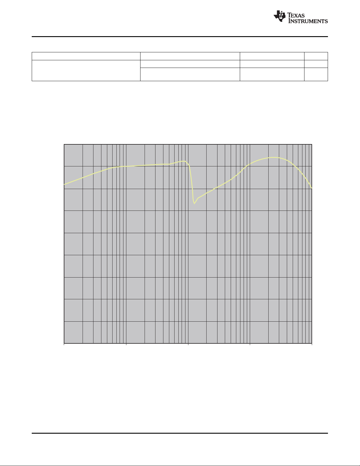
SWCS037-018
VDD1EFFICIENCY vsOUTPUT CURRENT
Outputvoltage=1.3V,Vbat=3.6V
90
80
70
60
50
40
30
20
10
00
0.0001 0.001 0.01 0.1 1
ILOAD(A)
Effciency(%)
TPS65930/TPS65920
SWCS037G–MAY 2008– REVISED APRIL 2011
Table 4-3. VDD1 dc-dc Regulator Characteristics (continued)
Parameter Comments Min Typ Max Unit
External capacitor
(5) Under current load condition step:
Imax/2 (550 mA) in 100 ns with a ±20% external capacitor accuracy or
Imax/3 (367 mA) in 100 ns with a ±50% external capacitor accuracy
(5)
Value 8 10 12 μF
Equivalent series resistance (ESR) at 0 20 mΩ
switching frequency
See Table 2-2 for how to connect the VDD1/2 dc-dc converter when it is not in use.
Figure 4-2 shows the efficiency of the VDD1 dc-dc regulator in active mode and sleep mode.
www.ti.com
Figure 4-2. VDD1 dc-dc Regulator Efficiency
4.1.1.2 External Components and Application Schematics
Figure 4-3 is an application schematic with the external components on the VDD1 dc-dc regulator.
30 Power Module Copyright © 2008–2011, Texas Instruments Incorporated
Submit Documentation Feedback
focus.ti.com: TPS65930/TPS65920
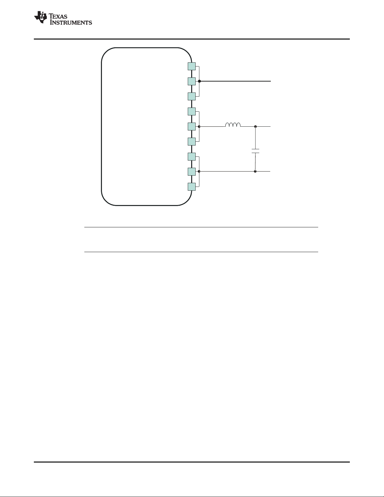
VDD1.IN (D14)
VDD1.SW (C11)
VDD1.GND (A12)
Device
VDD1.IN (D13)
VDD1.IN (D12)
VDD1.SW (C12)
VDD1.SW (C13)
VDD1.GND (B11)
VDD1.GND (B12)
030-009
L
VDD1
C
VDD1.OUT
TPS65930/TPS65920
www.ti.com
SWCS037G–MAY 2008– REVISED APRIL 2011
Figure 4-3. VDD1 dc-dc Application Schematic
For the component values, see Table 14-1.
NOTE
Copyright © 2008–2011, Texas Instruments Incorporated Power Module 31
Submit Documentation Feedback
focus.ti.com: TPS65930/TPS65920

TPS65930/TPS65920
SWCS037G–MAY 2008– REVISED APRIL 2011
www.ti.com
4.1.2 VDD2 dc-dc Regulator
4.1.2.1 VDD2 dc-dc Regulator Characteristics
The VDD2 dc-dc regulator is a programmable output stepdown dc-dc converter with an internal field effect
transistor (FET). Like the VDD1 regulator, the VDD2 regulator can be placed in sleep or power-down
mode and is SmartReflex-compatible. The VDD2 regulator differs from VDD1 in its current load capability.
Table 4-4 describes the regulator characteristics.
Table 4-4. VDD2 dc-dc Regulator Characteristics
Parameter Comments Min Typ Max Unit
Input voltage range 2.7 3.6 4.5 V
Output voltage 0.6 1 1.5 V
Output voltage step Covering the 0.6-V to 1.45-V range, 12.5 mV
Output accuracy
(1)
Switching frequency 3.2 MHz
Conversion efficiency
(2)
, Figure 4-4 in active mode
Output current
Ground current (IQ) Off at 30°C 1 μA
Short-circuit current VIN= V
Load regulation 0 < IO< I
Transient load regulation
(3)
Line regulation 10 mV
Transient line regulation 300 mVPPac input, 10-μs rise and fall 10 mV
Output shunt resistor (internal pulldown) 500 700 Ω
Start-up time 0.25 1 ms
Recovery time From sleep mode to on mode with 25 100 μs
Slew rate (rising or falling)
(4)
External coil DCR 0.1 Ω
External capacitor
(5)
(1) Accuracy includes all variations (line and load regulations, line and load transients, temperature, and process)
(2) VBAT = 3.8 V, VDD2 = 1.3 V, Fs = 3.2 MHz, L = 1 μH, L
(3) Output voltage needs to discharge the load current completely and settle to its final value within 100 μs.
(4) Load current varies proportionally with the output voltage. The slew rate is for both increasing and decreasing voltages and the
maximum load current is 600 mA.
(5) Under current load condition step:
Imax/2 (300 mA) in 100 ns with a ±20% external capacitor accuracy or
Imax/3 (200 mA) in 100 ns with a ±50% external capacitor accuracy
1.5 V is a single programmable value
0.6 V to < 0.8 V –6% 6%
0.8 V to 1.5 V –4% 4%
IO= 10 mA, sleep 82%
100 mA < IO< 300 mA 85%
300 mA < IO< 500 mA 80%
Active mode 600 mA
Sleep mode 10 mA
Sleep, unloaded 50
Active, unloaded, not switching 300
Max
Max
IO= 10 mA to (I
Maximum slew rate is I
/2) + 10 mA,
Max
/2/100 ns
Max
–65 50 mV
1.2 A
20 mV
time
constant load
4 8 16 mV/μs
Value 0.7 1 1.3 μH
Saturation current 900 mA
Value 8 10 12 μF
ESR at switching frequency 0 20 mΩ
= 100 mΩ, C = 10 μF, ESR = 10 mΩ
DCR
32 Power Module Copyright © 2008–2011, Texas Instruments Incorporated
Submit Documentation Feedback
focus.ti.com: TPS65930/TPS65920

SWCS037-019
VDD2EFFICIENCY vsOUTPUT CURRENT
Outputvoltage=1.3V,Vbat=3.6V
90
80
70
60
50
40
30
20
10
00
0.0001 0.001 0.01 0.1 1
ILOAD(A)
Effciency(%)
TPS65930/TPS65920
www.ti.com
See Table 2-2 for how to connect the VDD1/2 dc-dc converter when it is not in use.
Figure 4-4 shows the efficiency of the VDD2 dc-dc regulator in active mode and sleep mode.
SWCS037G–MAY 2008– REVISED APRIL 2011
Figure 4-4. VDD2 dc-dc Regulator Efficiency
4.1.2.2 External Components and Application Schematics
Figure 4-5 is an application schematic with the external components on the VDD2 dc-dc regulator.
Copyright © 2008–2011, Texas Instruments Incorporated Power Module 33
Submit Documentation Feedback
focus.ti.com: TPS65930/TPS65920

VDD2.IN (M12)
VDD2.SW (N11)
VDD2.GND (N12)
Device
VDD2.IN (M13)
VDD2.SW (P11)
VDD2.GND (P12)
030-010
L
VDD2
C
VDD2.OUT
TPS65930/TPS65920
SWCS037G–MAY 2008– REVISED APRIL 2011
www.ti.com
Figure 4-5. VDD2 dc-dc Application Schematic
NOTE
For the component values, see Table 14-1.
34 Power Module Copyright © 2008–2011, Texas Instruments Incorporated
Submit Documentation Feedback
focus.ti.com: TPS65930/TPS65920

TPS65930/TPS65920
www.ti.com
SWCS037G–MAY 2008– REVISED APRIL 2011
4.1.3 VIO dc-dc Regulator
4.1.3.1 VIO dc-dc Regulator Characteristics
The I/O and memory dc-dc regulator is a 600-mA stepdown dc-dc converter (internal FET) with two output
voltage settings. It supplies the memories and all I/O ports in the application and is one of the first power
providers to switch on in the power-up sequence. This dc-dc regulator can be placed in sleep or
power-down mode; however, care must be taken in the sequencing of this power provider, because
numerous ESD blocks are connected to this supply. Table 4-5 describes the regulator characteristics.
Table 4-5. VIO dc-dc Regulator Characteristics
Parameter Comments Min Typ Max Unit
Input voltage range 2.7 3.6 4.5 V
Output voltage
Output accuracy
Switching frequency 3.2 MHz
Conversion efficiency
Output current
Ground current (IQ) Off at 30°C 1 μA
Load transient
Line transient 300 mVPPac, input rise and fall time 10 μs 10 mV
Start-up time 0.25 1 ms
Recovery time From sleep mode to on mode with constant <10 100 μs
Output shunt resistor (internal pulldown) 500 700 Ω
External coil DCR 0.1 Ω
External capacitor
(1) This voltage is tuned according to the platform and transient requirements.
(2) ±4% accuracy includes all the variation (line and load regulation, line and load transient, temperature, process)
±3% accuracy is dc accuracy only.
(3) VBAT = 3.8 V, VIO = 1.8 V, Fs = 3.2 MHz, L = 1 μH, L
(4) Load transient can also be specified as 0 < IO< I
(1)
(2)
(3)
Figure 4-6 in active mode
(4)
IO= 10 mA, sleep 85%
100 mA < IO< 400 mA 85%
400 mA < IO< 600 mA 80%
On mode 700 mA
Sleep mode 10
Sleep, unloaded 50
Active, unloaded, not switching 300
load
Value 0.7 1 1.3 μH
Saturation current 900 mA
Value 8 10 12 μF
ESR at switching frequency 1 20 mΩ
= 100 mΩ, C = 10 μF, ESR = 10 mΩ
DCR
/2, Δt = 1 μs, 100 mV but this is not included in ±4% accuracy.
OUTmax
–4% 4%
–3% 3%
1.8
1.85
50 mV
V
Copyright © 2008–2011, Texas Instruments Incorporated Power Module 35
Submit Documentation Feedback
focus.ti.com: TPS65930/TPS65920

SWCS037-020
VIOEFFICIENCY vsOUTPUT CURRENT
Outputvoltage=1.2V,Vbat=3.8V
90
80
70
60
50
40
30
20
10
00
0.0001 0.001 0.01 0.1 1
ILOAD(A)
Effciency(%)
100
TPS65930/TPS65920
SWCS037G–MAY 2008– REVISED APRIL 2011
Figure 4-6 shows the efficiency of the VIO dc-dc regulator in active mode and sleep mode.
www.ti.com
Figure 4-6. VIO dc-dc Regulator Efficiency
4.1.3.2 External Components and Application Schematics
Figure 4-7 is an application schematic with the external components on the VIO dc-dc regulator.
36 Power Module Copyright © 2008–2011, Texas Instruments Incorporated
Submit Documentation Feedback
focus.ti.com: TPS65930/TPS65920

VIO.IN (M2)
VIO.SW (N4)
VIO.GND (N3)
Device
VIO.IN (M3)
VIO.SW (P4)
VIO.GND (P3)
030-011
L
VIO
C
VIO.OUT
TPS65930/TPS65920
www.ti.com
SWCS037G–MAY 2008– REVISED APRIL 2011
Figure 4-7. VIO dc-dc Application Schematic
NOTE
For the component values, see Table 14-1.
Copyright © 2008–2011, Texas Instruments Incorporated Power Module 37
Submit Documentation Feedback
focus.ti.com: TPS65930/TPS65920

TPS65930/TPS65920
SWCS037G–MAY 2008– REVISED APRIL 2011
4.1.4 VDAC LDO Regulator
The VDAC programmable LDO regulator is a high-PSRR, low-noise linear regulator that powers the host
processor dual-video DAC. It is controllable with registers through I2C and can be powered down.
Table 4-6 describes the regulator characteristics.
Table 4-6. VDAC LDO Regulator Characteristics
Parameter Test Conditions Min Typ Max Unit
Output Load Conditions
Filtering capacitor Connected from VDAC.OUT to analog ground 0.3 1 2.7 μF
Filtering capacitor ESR 20 600 mΩ
Electrical Characteristics
V
Input voltage 2.7 3.6 4.5 V
IN
V
Output voltage On mode 1.164 1.2 1.236 V
OUT
I
Rated output current On mode 70 mA
OUT
dc load regulation On mode: 0 < IO< I
dc line regulation On mode, VIN= V
Turn-on time I
Wake-up time Full load capability 10 μs
Ripple rejection f < 20 kHz 65 dB
Output noise 100 Hz < f < 5 kHz 400 nV/√Hz
Ground current On mode, I
V
Dropout voltage On mode, I
DO
Transient load regulation –40 40 mV
Transient line regulation 10 mV
1.261 1.3 1.339
1.746 1.8 1.854
Low-power mode 5
Max
to V
INmin
= 0, CL= 1 μF (within 10% of V
OUT
INmax
at I
= I
OUT
OUTmax
) 100 μs
OUT
20 mV
20 kHz < f < 100 kHz 45
f = 1 MHz 40
VIN= V
+ 1 V, IO= I
OUT
Max
5 kHz < f < 400 kHz 125
400 kHz < f < 10 MHz 50
= 0 150 μA
OUT
On mode, I
Low-power mode, I
Low-power mode, I
OUT
= I
OUTmax
= 0 15
OUT
= 1 mA 25
OUT
350
Off mode at 55°C 1
OUT
I
: I
Min
– I
Max
Load
Slew: 60 mA/μs
= I
OUTmax
250 mV
VINdrops 500 mV
Slew: 40 mV/μs
www.ti.com
3 mV
38 Power Module Copyright © 2008–2011, Texas Instruments Incorporated
Submit Documentation Feedback
focus.ti.com: TPS65930/TPS65920

TPS65930/TPS65920
www.ti.com
4.1.5 VPLL1 LDO Regulator
The VPLL1 programmable LDO regulator is a high-PSRR, low-noise, linear regulator used for the host
processor PLL supply. Table 4-7 describes the regulator characteristics.
Table 4-7. VPLL1 LDO Regulator Characteristics
Parameter Test Conditions Min Typ Max Unit
Output Load Conditions
Filtering capacitor Connected from VPLL1.OUT to analog ground 0.3 1 2.7 μF
Filtering capacitor ESR 20 600 mΩ
Electrical Characteristics
V
Input voltage 2.7 3.6 4.5 V
IN
V
Output voltage On mode and low-power mode 0.97 1.0 1.03 V
OUT
I
Rated output current On mode 40 mA
OUT
dc load regulation On mode: 0 < IO< I
dc line regulation On mode, VIN= V
Turn-on time I
Wake-up time Full load capability 10 μs
Ripple rejection f < 10 kHz 50 dB
Ground current On mode, I
V
Dropout voltage On mode, I
DO
Transient load regulation –40 40 mV
Transient line regulation 10 mV
SWCS037G–MAY 2008– REVISED APRIL 2011
1.164 1.2 1.236
1.261 1.3 1.339
1.746 1.8 1.854
2.716 2.8 2.884
2.91 3.0 3.090
Low-power mode 5
Max
to V
INmin
= 0, CL= 1 μF (within 10% of V
OUT
INmax
at I
= I
OUT
OUTmax
) 100 μs
OUT
20 mV
10 kHz < f < 100 kHz 40
f = 1 MHz 30
VIN= V
On mode, I
Low-power mode, I
Low-power mode, I
+ 1 V, IO= I
OUT
OUT
OUT
Max
= 0 70 μA
= I
OUTmax
= 0 15
OUT
= 1 mA 16
OUT
110
Off mode at 55°C 1
OUT
I
: I
Min
– I
Max
Load
Slew: 60 mA/μs
= I
OUTmax
250 mV
VINdrops 500 mV
Slew: 40 mV/μs
3 mV
Copyright © 2008–2011, Texas Instruments Incorporated Power Module 39
Submit Documentation Feedback
focus.ti.com: TPS65930/TPS65920

TPS65930/TPS65920
SWCS037G–MAY 2008– REVISED APRIL 2011
4.1.6 VMMC1 LDO Regulator
The VMMC1 LDO regulator is a programmable linear voltage converter that powers the multimedia card
(MMC) slot. It includes a discharge resistor and overcurrent protection (short-circuit). This LDO regulator
can also be turned off automatically when MMC card extraction is detected. The VMMC1 LDO can be
powered through an independent supply other than the battery; for example, a charge pump. In this case,
the input from the VMMC1 LDO can be higher than the battery voltage. Table 4-8 describes the regulator
characteristics.
Table 4-8. VMMC1 LDO Regulator Characteristics
Parameter Test Conditions Min Typ Max Unit
Output Load Conditions
Filtering capacitor Connected from VMMC1.OUT to analog ground 0.3 1 2.7 μF
Filtering capacitor ESR 20 600 mΩ
Electrical Characteristics
V
Input voltage 2.7 3.6 5.5 V
IN
V
Output voltage On mode and low-power mode V
OUT
I
Rated output current mA
OUT
dc load regulation On mode: 0 < IO< I
dc line regulation On mode, VIN= V
Turn-on time I
Wake-up time Full load capability 10 μs
Ripple rejection dB
Ground current Low-power mode, I
V
Dropout voltage On mode, I
DO
Transient load regulation –40 40 mV
Transient line regulation 10 mV
1.7945 1.85 1.9055
2.7645 2.85 2.9355
2.91 3.0 3.09
3.0555 3.15 3.2445
On mode 220
Low-power mode 5
Max
to V
INmin
= 0, CL= 1 μF (within 10% of V
OUT
INmax
at I
= I
OUT
OUTmax
) 100 μs
OUT
20 mV
f < 10 kHz 50
10 kHz < f < 100 kHz 40
f = 1 MHz 25
VIN= V
On mode, I
On mode, I
Low-power mode, I
Off mode at 55°C 1
I
Load
Slew: 40 mA/μs
: I
Min
+ 1 V, IO= I
OUT
– I
OUT
OUT
OUT
Max
Max
= 0 70
= I
OUTmax
= 0 17 μA
OUT
= 5 mA 20
OUT
= I
OUTmax
290
250 mV
VINdrops 500 mV
Slew: 40 mV/μs
www.ti.com
3 mV
40 Power Module Copyright © 2008–2011, Texas Instruments Incorporated
Submit Documentation Feedback
focus.ti.com: TPS65930/TPS65920

TPS65930/TPS65920
www.ti.com
4.1.7 VAUX2 LDO Regulator
The VAUX2 general-purpose LDO regulator powers the auxiliary devices. Table 4-9 describes the
regulator characteristics.
Table 4-9. VAUX2 LDO Regulator Characteristics
Parameter Test Conditions Min Typ Max Unit
Output Load Conditions
Filtering capacitor Connected from VAUX2.OUT to analog ground 0.3 1 2.7 μF
Filtering capacitor ESR 20 600 mΩ
Electrical Characteristics
V
Input voltage 2.7 3.6 4.5 V
IN
V
Output voltage On mode and low-power mode –3% 3% V
OUT
I
Rated output current mA
OUT
dc load regulation On mode: I
dc line regulation On mode, VIN= V
Turn-on time I
Wake-up time Full load capability 10 μs
Ripple rejection dB
Ground current Low-power mode, I
V
Dropout voltage On mode, I
DO
Transient load regulation –40 40 mV
Transient line regulation 10 mV
SWCS037G–MAY 2008– REVISED APRIL 2011
1.3
1.5
1.7
1.8
1.9
2.0
2.1
2.2
2.3
2.4
2.5
2.8
On mode 100
Low-power mode 5
= I
OUT
= 0, CL= 1 μF (within 10% of V
OUT
to 0 20 mV
OUTmax
INmin
to V
INmax
at I
= I
OUT
OUTmax
) 100 μs
OUT
f < 10 kHz 50
10 kHz < f < 100 kHz 40
f = 1 MHz 25
VIN= V
On mode, I
On mode, I
Low-power mode, I
Off mode at 55°C 1
I
Load
Slew: 40 mA/μs
: I
Min
+ 1 V, IO= I
OUT
– I
OUT
OUT
OUT
Max
Max
= 0 70
= I
OUTmax
= 0 17 μA
OUT
= 5 mA 20
OUT
= I
OUTmax
170
250 mV
VINdrops 500 mV
Slew: 40 mV/μs
3 mV
Copyright © 2008–2011, Texas Instruments Incorporated Power Module 41
Submit Documentation Feedback
focus.ti.com: TPS65930/TPS65920
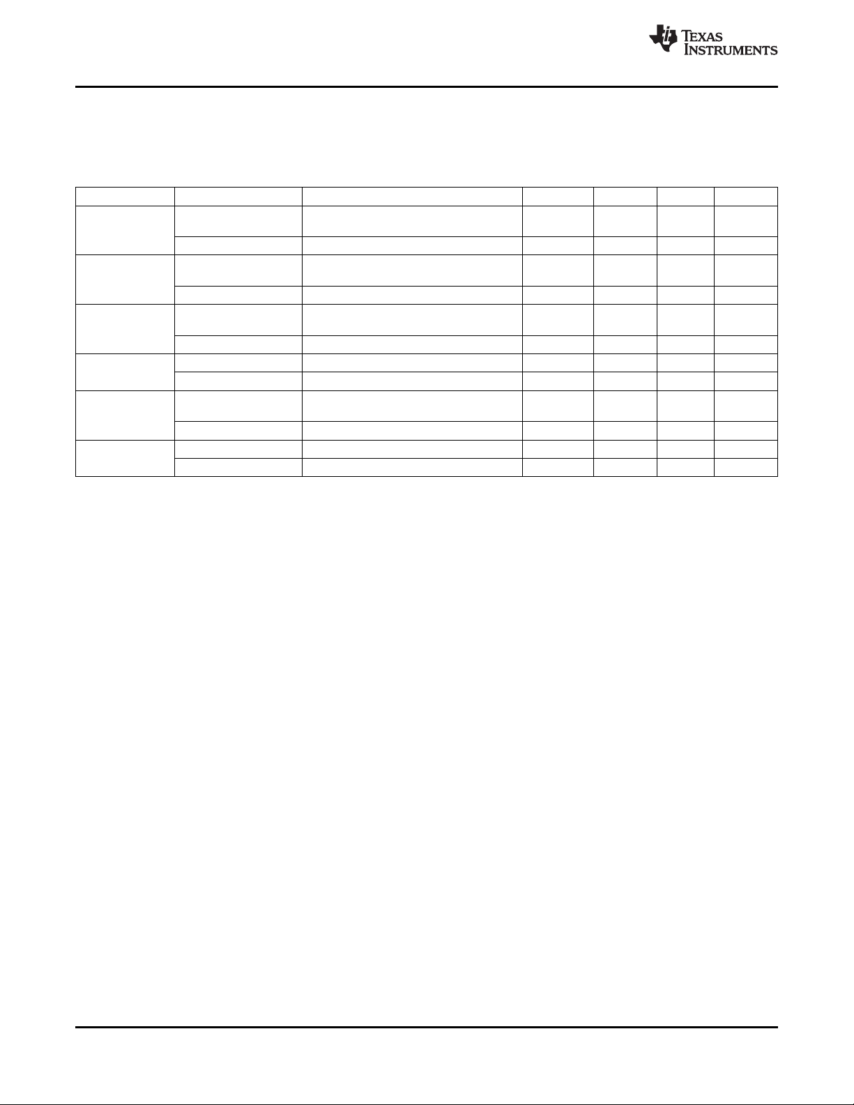
TPS65930/TPS65920
SWCS037G–MAY 2008– REVISED APRIL 2011
www.ti.com
4.1.8 Output Load Conditions
Table 4-10 lists the regulators that power the device, and the output loads associated with them.
Table 4-10. Output Load Conditions
Regulator Parameter Test Conditions Min Typ Max Unit
VINTDIG LDO Filtering capacitor Connected from VINTDIG.OUT to analog 0.3 1 2.7 μF
Filtering capacitor ESR 20 600 mΩ
VINTANA1 LDO Filtering capacitor Connected from VINTANA1.OUT to 0.3 1 2.7 μF
Filtering capacitor ESR 20 600 mΩ
VINTANA2 LDO Filtering capacitor Connected from VINTANA2.OUT to 0.3 1 2.7 μF
Filtering capacitor ESR 20 600 mΩ
VRUSB_3V1 LDO Filtering capacitor Connected from VUSB.3P1 to GND 0.3 1 2.7 μF
Filtering capacitor ESR 0 10 600 mΩ
VRUSB_1V8 LDO Filtering capacitor Connected from VINTUSB1P8.OUT to 0.3 1 2.7 μF
Filtering capacitor ESR 0 10 600 mΩ
VRUSB_1V5 LDO Filtering capacitor Connected from VINTUSB1P5 to GND 0.3 1 2.7 μF
Filtering capacitor ESR 0 10 600 mΩ
ground
analog ground
analog ground
GND
42 Power Module Copyright © 2008–2011, Texas Instruments Incorporated
Submit Documentation Feedback
focus.ti.com: TPS65930/TPS65920
TPS65930/TPS65920
www.ti.com
4.1.9 Charge Pump
The charge pump generates a 4.8-V (nominal) power supply voltage from the battery to the VBUS pin.
The input voltage range is 2.7 to 4.5 V for the battery voltage. The charge pump operating frequency is
1 MHz.
The charge pump tolerates 7 V on VBUS when it is in power-down mode. The charge pump integrates a
short-circuit current limitation at 450 mA. Table 4-11 lists the charge pump output load conditions.
Parameter Test Conditions Min Typ Max Unit
Output Load Conditions
Filtering capacitor Connected from VBUS to VSSP 1.41 4.7 6.5 μF
Flying capacitor Connected from CP to CN 1.32 2.2 3.08 μF
Filtering capacitor ESR 20 mΩ
SWCS037G–MAY 2008– REVISED APRIL 2011
Table 4-11. Charge Pump Output Load Conditions
Copyright © 2008–2011, Texas Instruments Incorporated Power Module 43
Submit Documentation Feedback
focus.ti.com: TPS65930/TPS65920

TPS65930/TPS65920
SWCS037G–MAY 2008– REVISED APRIL 2011
4.1.10 USB LDO Short-Circuit Protection Scheme
The short-circuit current for the LDOs and dc-dcs in the TPS65920 and TPS65930 devices is
approximately twice the maximum load current. When the output of the block is shorted to ground, the
power dissipation can exceed the 1.2-W requirement if no action is taken. A short-circuit protection
scheme is included in the TPS65920 and TPS65930 devices to ensure that if the output of an LDO or
dc-dc is short-circuited, the power dissipation does not exceed the 1.2-W level.
The three USB LDOs, VRUSB3V1, VRUSB1V8, and VRUSB1V5, are included in this short-circuit
protection scheme, which monitors the LDO output voltage at a frequency of 1 Hz and generates an
interrupt (sc_it) when a short-circuit is detected.
The scheme compares the LDO output voltage to a reference voltage and detects a short-circuit if the
LDO voltage drops below this reference value (0.5 or 0.75 V programmable). In the case of the
VRUSB3V1 and VRUSB1V8 LDOs, the reference is compared with a divided down voltage (1.5 V typical).
If a short-circuit is detected on VRUSB3V1, the power subchip FSM switches this LDO to sleep mode.
If a short-circuit is detected on VRUSB1V8 or VRUSB1V5, the power subchip FSM switches off the
relevant LDO.
www.ti.com
44 Power Module Copyright © 2008–2011, Texas Instruments Incorporated
Submit Documentation Feedback
focus.ti.com: TPS65930/TPS65920
TPS65930/TPS65920
www.ti.com
SWCS037G–MAY 2008– REVISED APRIL 2011
4.2 Power References
The bandgap voltage reference is filtered (resistance/capacitance [RC] filter) using an external capacitor
connected across the VREF output and an analog ground (REFGND). The VREF voltage is scaled,
distributed, and buffered in the device. The bandgap is started in fast mode (not filtered), and is set
automatically by the power state-machine in slow mode (filtered, less noisy) when required.
Table 4-12 lists the voltage reference characteristics.
Table 4-12. Voltage Reference Characteristics
Parameter Test Conditions Min Typ Max Unit
Output Load Condition
Filtering capacitor Connected from V
Electrical Characteristics
VINInput voltage On mode 2.7 3.6 4.5 V
Internal bandgap reference voltage On mode, measured through TESTV terminal 1.272 1.285 1.298 V
Reference voltage (V
Retention mode reference On mode 0.492 0.5 0.508 V
I
NMOS sink 0.9 1 1.1 μA
REF
Ground current Bandgap 25 μA
Output spot noise 100 Hz 1 μV/√Hz
A-weighted noise (rms) 200 nV (rms)
P-weighted noise (rms) 150 nV (rms)
Integrated noise 20 to 100 kHz 2.2 μV
I
trim bit LSB 0.1 μA
BIAS
Ripple rejection <1 MHz from VBAT 60 dB
Start-up time 1 ms
terminal) On mode 0.749 0.75 0.77 V
REF
I
block 20
REF
Preregulator 15
V
buffer 10
REF
Retention reference buffer 10
to GNDREF 0.3 1 2.7 μF
REF
4.3 Power Control
4.3.1 Backup Battery Charger
If the backup battery is rechargeable, it can be recharged from the main battery. A programmable voltage
regulator powered by the main battery allows recharging of the backup battery. The backup battery charge
must be enabled using a control bit register. Recharging starts when two conditions are met:
• Main battery voltage > backup battery voltage
• Main battery > 3.2 V
The comparators of the backup battery system (BBS) give the two thresholds of the backup battery charge
startup. The programmed voltage for the charger gives the end-of-charge threshold. The programmed
current for the charger gives the charge current.
Overcharging is prevented by measurement of the backup battery voltage through the GP ADC.
Table 4-13 lists the characteristics of the backup battery charger.
Table 4-13. Backup Battery Charger Characteristics
Parameter Test Conditions Min Typ Max Unit
VBACKUP-to-MADC input attenuation VBACKUP from 1.8 to 3.3 V 0.33 V/V
Copyright © 2008–2011, Texas Instruments Incorporated Power Module 45
Submit Documentation Feedback
focus.ti.com: TPS65930/TPS65920
TPS65930/TPS65920
SWCS037G–MAY 2008– REVISED APRIL 2011
www.ti.com
Table 4-13. Backup Battery Charger Characteristics (continued)
Parameter Test Conditions Min Typ Max Unit
Backup battery charging current VBACKUP = 2.8 V, BBCHEN = 1, BBISEL = 00 10 25 45 μA
VBACKUP = 2.8 V, BBCHEN = 1, BBISEL = 01 105 150 270 μA
VBACKUP = 2.8 V, BBCHEN = 1, BBISEL = 10 350 500 900 μA
VBACKUP = 2.8 V, BBCHEN = 1, BBISEL = 11 0.7 1 1.8 mA
VBACKUP = 0 V, BBCHEN = 1, BBISEL = 00 17.5 25 45 μA
VBACKUP = 0 V, BBCHEN = 1, BBISEL = 01 105 150 270 μA
VBACKUP = 0 V, BBCHEN = 1, BBISEL = 10 350 500 900 μA
VBACKUP = 0 V, BBCHEN = 1, BBISEL = 11 0.7 1 1.8 mA
End backup battery charging voltage: I
VBBCHGEND
VBACKUP
I
VBACKUP
I
VBACKUP
I
VBACKUP
= –10 μA, BBSEL = 00 2.4 2.5 2.6 V
= –10 μA, BBSEL = 01 2.9 3.0 3.1 V
= –10 μA, BBSEL = 10 3.0 3.1 3.2 V
= –10 μA, BBSEL = 11 3.1 3.2 3.3 V
4.3.2 Battery Monitoring and Threshold Detection
4.3.2.1 Power On/Power Off and Backup Conditions
Table 4-14 lists the threshold levels of the battery.
Table 4-14. Battery Threshold Levels
Parameter Test Conditions Min Typ Max Unit
Main battery charged threshold Measured on VBAT terminal 3.1 3.2 3.3 V
VMBCH
Main battery low threshold VMBLO VBACKUP = 3.2 V, measured on VBAT terminal (monitored 2.55 2.7 2.85 V
Main battery high threshold VMBHI Measured on terminal VBAT, VBACKUP = 0 V 2.5 2.65 2.95 V
Batteries not present threshold VBNPR Measured on terminal VBACKUP with VBAT < 2.1 V 1.6 1.8 2.0 V
on terminal ONNOFF)
Measured on terminal VBAT, VBACKUP = 3.2 V 2.5 2.85 2.95
Measured on terminal VBAT with VBACKUP = 0 V 1.95 2.1 2.25
(monitored on terminal VRRTC)
4.3.3 VRRTC LDO Regulator
The VRRTC voltage regulator is a programmable, low dropout, linear voltage regulator supplying (1.5 V)
the embedded real-time clock (32.768-kHz oscillator) and dedicated I/Os of the digital host counterpart.
The VRRTC regulator is also the supply voltage of the power-management digital state-machine. The
VRRTC regulator is supplied from the UPR line, switched on by the main or backup battery, depending on
the system state. The VRRTC output is present as long as a valid energy source is present. The VRRTC
line is supplied by an LDO when VBAT > 2.7, and a clamp circuit when in backup mode. Table 4-15
describes the regulator characteristics.
Table 4-15. VRRTC LDO Regulator Characteristics
Parameter Test Conditions Min Typ Max Unit
Output Load Conditions
Filtering capacitor Connected from VRTC.OUT to analog ground 0.3 1 2.7 μF
Filtering capacitor ESR 20 600 mΩ
Electrical Characteristics
V
IN
V
OUT
Input voltage On mode 2.7 VBAT 4.5 V
Output voltage On mode 1.45 1.5 1.55 V
46 Power Module Copyright © 2008–2011, Texas Instruments Incorporated
Submit Documentation Feedback
focus.ti.com: TPS65930/TPS65920
TPS65930/TPS65920
www.ti.com
Table 4-15. VRRTC LDO Regulator Characteristics (continued)
Parameter Test Conditions Min Typ Max Unit
I
OUT
V
DO
(1) For nominal output voltage
Rated output current On mode 30 mA
DC load regulation On mode: I
DC line regulation On mode, VIN= V
Turn-on time I
Wake-up time On mode from low power to On mode, I
Ripple rejection (VRRTC) f < 10 kHz 50 dB
Ground current On mode, I
Dropout voltage
(1)
Transient load regulation I
Transient line regulation VINdrops 500 mV 10 mV
Overshoot Softstart 3%
Pull down resistance Default in off mode 250 320 450 Ω
SWCS037G–MAY 2008– REVISED APRIL 2011
Sleep mode 1
= I
OUT
= 0, at V
OUT
V
OUT
= V
OUT
OUTfinal
± 3%
From backup to On mode, I
V
OUTfinal
± 3%
to 0 100 mV
OUTmax
INmin
= V
to V
OUTfinal
at I
INmax
OUT
= I
OUTmax
± 3% 100 μs
= 0, at 100 μs
OUT
OUT
= 0, at V
= 100
OUT
100 mV
10 kHz < f < 100 kHz 40
f = 1 MHz 30
VIN= V
On mode, I
Sleep mode, I
Sleep mode, I
+ 1 V, IO= I
OUT
OUT
OUT
OUT
OUT
MAX
= 0 70 μA
= I
OUTmax
= 0 10
= 1 mA 11
100
Off mode 1
On mode, I
: I
LOAD
MIN
Slew: 40 mA/μs
OUT
– I
MAX
= I
OUTmax
250 mV
–40 40 mV
Slew: 40 mV/μs
4.4 Power Consumption
Table 4-16 describes the power consumption depending on the use cases.
NOTE
Typical power consumption is obtained in the nominal operating conditions and with the
TPS65920 and TPS65930 devices in stand-alone configuration.
Table 4-16. Power Consumption
Mode Description Typical Consumption
Backup domain. No main source is connected. Consumption is on the backup VBAT not present 2.25 * 3.2 = 7.2 μW
Wait on VBAT = 3.8 V 64 × 3.8 = 243.2 μW
Active no load with full current capability, internal reset is released, and the associated VBAT = 3.8 V 3291 × 3.8 = 12505 μW
Sleep no load in low-consumption mode, and the associated processor is in low-power VBAT = 3.8 V 496 × 3.8 = 1884.4 μW
Only the RTC date is maintained with a couple of registers in the backup
battery.
The phone is apparently off for the user, a main battery is present and
well-charged. The RTC registers and registers in the backup domain are
maintained. The wake-up capabilities (such as the PWRON button) are
available.
The subsystem is powered by the main battery, all supplies are enabled
processor is running.
The main battery powers the subsystem, selected supplies are enabled but
mode.
Copyright © 2008–2011, Texas Instruments Incorporated Power Module 47
Submit Documentation Feedback
focus.ti.com: TPS65930/TPS65920

TPS65930/TPS65920
SWCS037G–MAY 2008– REVISED APRIL 2011
Table 4-17 lists the regulator states according to the mode in use.
Table 4-17. Regulator State Depending on Use Case
Regulator
VAUX2 OFF OFF SLEEP ON
VMMC1 OFF OFF OFF OFF
VPLL1 OFF OFF SLEEP ON
VDAC OFF OFF OFF OFF
VINTANA1 OFF OFF SLEEP ON
VINTANA2 OFF OFF SLEEP ON
VINTDIG OFF OFF SLEEP ON
VIO OFF OFF SLEEP ON
VDD1 OFF OFF SLEEP ON
VDD2 OFF OFF SLEEP ON
VUSB_1V5 OFF OFF OFF OFF
VUSB_1V8 OFF OFF OFF OFF
VUSB_3V1 OFF OFF SLEEP SLEEP
www.ti.com
Mode
Backup Wait On Sleep No Load Active No Load
48 Power Module Copyright © 2008–2011, Texas Instruments Incorporated
Submit Documentation Feedback
focus.ti.com: TPS65930/TPS65920

TPS65930/TPS65920
www.ti.com
4.5 Power Management
4.5.1 Boot Modes
Table 4-18 lists the modes corresponding to BOOT0–BOOT1.
Name Description BOOT0 BOOT1
MC027 Master_C027_Generic 01 0 1
MC021 Master_C021_Generic 10 1 0
SC021 Slave_C021_Generic 11 1 1
4.5.2 Process Modes
This parameter defines:
• The boot voltage for the host core
• The boot sequence associated with the process
• The dynamic voltage and frequency scaling (DVFS) protocol associated with the process
4.5.2.1 MC021 Mode
SWCS037G–MAY 2008– REVISED APRIL 2011
Table 4-18. BOOT Mode Description
Reserved 0 0
Table 4-19 lists the characteristics of MC021 mode.
Boot core voltage 1.2 V
Power sequence VIO followed by VPLL1, VDD2, VDD1
DVFS protocol SmartReflex IF (I2C HS)
4.5.3 Power-On Sequence
4.5.3.1 Timing Before Sequence_Start
Sequence_Start is a symbolic internal signal to ease the description of the power sequences. It occurs
according to the events shown in Figure 4-8.
Table 4-19. MC021 Mode
Copyright © 2008–2011, Texas Instruments Incorporated Power Module 49
Submit Documentation Feedback
focus.ti.com: TPS65930/TPS65920

Vbkup
User_Action
Vbat
Sequence_Start
VAC
Sequence_Start
PWRON
Sequence_Start
PWRON
Sequence_Start
Pushbuttondebouncing-30ms
0 ms
Starting_Eventismainbatteryinsertion
Starting_EventisPWRONbutton
Starting_Eventischargerinsertion
Starting_EventisPWRONrisingwhendeviceisinslavemode
61 ms-2cycle32k
61 ms-2cycle32k
Vbus
Sequence_Start
Starting_EventisVBUSinsertion
61 ms-2cycle32k
030-012
TPS65930/TPS65920
SWCS037G–MAY 2008– REVISED APRIL 2011
www.ti.com
Figure 4-8. Timing Before Sequence Start
50 Power Module Copyright © 2008–2011, Texas Instruments Incorporated
Submit Documentation Feedback
focus.ti.com: TPS65930/TPS65920

Sequence_Start
REGEN
VIO
VPLL1
VDD2
VDD1
32K OUTCLK
SYSEN
CLKEN
HFCLKOUT
NRESPWRON
4608 msbatterydetection
1068 ms-3MHzoscillatorsetting+clockswitch
1099 msforVDD2stabilizationandVDD1startramping
1179 msforVIOstabilization
1022 msforLDOstabilizationandstartdc-dcramping
61 ms
~5.3ms
61 ms
1953 ms
1175 msforVDD1stabilization
1179 msforVIOstabilization
1.8V
1.8V
1.2V
1.2V
019-072
TPS65930/TPS65920
www.ti.com
4.5.3.2 Power-On Sequence
Figure 4-9 describes the timing and control that must occur in the OMAP3 mode. Sequence_Start is a
symbolic internal signal to ease the description of the power sequences. It occurs according to the events
shown in Figure 4-8.
SWCS037G–MAY 2008– REVISED APRIL 2011
Figure 4-9. Timings–Power On in OMAP3 Mode
4.5.3.3 Power On in Slave_C021 Mode
Figure 4-10 describes the timing and control that must occur in the Slave_C021 mode. Sequence_Start is
a symbolic internal signal to ease the description of the power sequences and occurs according to the
different events detailed in Figure 4-8
Copyright © 2008–2011, Texas Instruments Incorporated Power Module 51
Submit Documentation Feedback
focus.ti.com: TPS65930/TPS65920

030-022
PWRON
REGEN
VIO
VPLL1
VDD2
VDD1
32KCLKOUT
SYSEN
CLKEN
HFCLKOUT
NRESPWRON
4791 s – 3MHzoscillatorsetting+internalregm
1068 sforexternalsupplyrampm
1099 sforVDD2stabilizationm
1179 sforVIOdc-dcstablilizationm
1022 sm
1099 sforVDD2stabilizationm
61 sm
1175 sforVDD1stabilizationm
1953 sfordigitalclocksettingm
64 sm
1.8V
1.8V
1.2V
1.2V
TPS65930/TPS65920
SWCS037G–MAY 2008– REVISED APRIL 2011
www.ti.com
Figure 4-10. Timings—Power On in Slave_C021 Mode
52 Power Module Copyright © 2008–2011, Texas Instruments Incorporated
Submit Documentation Feedback
focus.ti.com: TPS65930/TPS65920

VBAT
DEVOFF(register)
NRESPWRON
REGEN
32K OUTCLK
DCDCs
LDOs
SYSEN
HFCLKOUT
CLKEN
NEXT_Startup_event
18 sm
1.2ms
1.2ms
1.2ms
18 sm
18 sm
18 sm
3.42msbeforedetectionofstartingevent
126 sm
037-055
TPS65930/TPS65920
www.ti.com
4.5.4 Power-Off Sequence
This section describes the signal behavior required to power down the system.
4.5.4.1 Power-Off Sequence
Figure 4-11 shows the timing and control that occur during the power-off sequence in master modes.
SWCS037G–MAY 2008– REVISED APRIL 2011
NOTE: All of these timings are typical values with the default setup (depending on the resynchronization between power
Copyright © 2008–2011, Texas Instruments Incorporated Power Module 53
domains, state machinery priority, etc.).
Figure 4-11. Power-Off Sequence in Master Modes
Because of the internal frequency used by Power STM switching from 3 to 1.5 MHz when the HF clock
value is 19.2 MHz, if the HF clock value is not 19.2 MHz (with HFCLK_FREQ bit field values set
accordingly in the CFG_BOOT register), the delay between DEVOFF and
NRESPWRON/CLK32KOUT/SYSEN/HFCLKOUT is divided by two (approximately 9 μs).
The DEVOFF event is PWRON falling edge in slave mode and DEVOFF internal register write in master
mode.
Submit Documentation Feedback
focus.ti.com: TPS65930/TPS65920

TPS65930/TPS65920
SWCS037G–MAY 2008– REVISED APRIL 2011
5 Real-Time Clock and Embedded Power Controller
The TPS65930 and TPS65920 devices contain an RTC to provide clock and timekeeping functions and an
EPC to provide battery supervision and control.
5.1 RTC
The RTC provides the following basic functions:
• Time information (seconds/minutes/hours) directly in binary-coded decimal (BCD) code
• Calendar information (day/month/year/day of the week) directly in BCD code
• Interrupt generation periodically (1 second/1 minute/1 hour/1 day) or at a precise time (alarm function)
• 32-kHz oscillator drift compensation and time correction
• Alarm-triggered system wake-up event
5.1.1 Backup Battery
The TPS65030 and TPS65920 devices device implement a backup mode in which a backup battery can
keep the RTC running to maintain clock and time information even if the main supply is not present. If the
backup battery is rechargeable, the device also provides a backup battery charger so it can be recharged
when the main battery supply is present.
The backup domain powers the following:
• Internal 32.768-kHz crystal oscillator
• RTC
• Eight general-purpose (GP) storage registers
• Backup domain low-power regulator (VBRTC)
www.ti.com
5.2 EPC
The EPC provides five system states for optimal power use by the system, as listed in Table 5-1.
Three categories of events can trigger state transitions:
• Hardware events: Supply/battery insertion, wake-up requests, USB plug, and RTC alarm
• Software events: Switch-off commands, switch-on commands, and sleep on commands
• Monitoring events: Supply/battery level check, main battery removal, main battery fail, and thermal
Table 5-1. System States
System State Description
NO SUPPLY The system is not powered by any battery.
BACKUP The system is powered only with the backup battery and maintains
only the VBRTC supply.
WAIT-ON The system is powered by the main battery and maintains only the
VRRTC supply. It can accept switch-on requests.
ACTIVE The system is powered by the main battery; all supplies can be
enabled with full current capability.
SLEEP The main battery powers the system; selected supplies are enabled,
but in low consumption mode.
shutdown
54 Real-Time Clock and Embedded Power Controller Copyright © 2008–2011, Texas Instruments Incorporated
Submit Documentation Feedback
focus.ti.com: TPS65930/TPS65920

Mainmic
Monauralauxiliary
input
Audio
TDM/I2S
interface
High-speed
I C
2
(Control)
Audio/voicemodule
HFCLKIN
BiasLDOs
Carkit
Speak/mic
H-bridge
vibrator
Device
037-004
Class-Dpredriver
TPS65930/TPS65920
www.ti.com
6 Audio/Voice Module (TPS65930 Device Only)
NOTE
This section applies only to the TPS65930 device.
Figure 6-1 is the audio/voice module block diagram.
SWCS037G–MAY 2008– REVISED APRIL 2011
Figure 6-1. Audio/Voice Module Block Diagram
6.1 Audio/Voice Downlink (RX) Module
The audio/voice module includes the following output stages:
• Predriver output signals for external class-D amplifiers (single-ended)
• Vibrator H-bridge
6.1.1 Predriver for External Class-D Amplifier
The external class-D amplifiers provide a stereo signal on terminals PreD.LEFT and PreD.RIGHT to drive
the external class-D amplifier. These terminals are available if a stereo, single-ended, ac-coupled headset
is used.
Copyright © 2008–2011, Texas Instruments Incorporated Audio/Voice Module (TPS65930 Device Only) 55
Submit Documentation Feedback
focus.ti.com: TPS65930/TPS65920

PreDriverD
Onboard
Chip
ClassD
(TPA2010D1...)
IN+
IN–
Closedto
external
ClassC
C /C
PL PR
037-054
C /C
PR.O PL.O
R /R
PL.O PR.O
C /C
PL.M PR.M
R /R
PR PL
R /R
PR.M PL.M
TPS65930/TPS65920
SWCS037G–MAY 2008– REVISED APRIL 2011
www.ti.com
6.1.1.1 Predriver Output Characteristics
Table 6-1 lists the predriver output characteristics.
Table 6-1. Predriver Output Characteristics
Parameter Test Conditions Min Typ Max Unit
Load impedance 10 kΩ
50 pF
Gain range
Absolute gain error –1 1 dB
Peak-to-peak output voltage (0 dBFs) Default gain
Total harmonic distortion At 0 dBFs –80 –75 dB
Default gain
Load > 10 kΩ // 50 pF At –20 dBFs –70 –65
Idle channel noise (20 Hz to 20 kHz, A-weighted)
SNR (A-weighted over 20-kHz bandwidth) At 0 dBFs 83 88 dB
Default gain
Output PSRR (for all gains) 20 Hz to 4 kHz 90 dB
(1) Audio digital filter = –62 to 0 dB (1-dB steps) and 0 to 12 dB (6-dB steps)
(2) The default gain setting assumes the ARXPGA has 0-dB gain setting (volume control) and output driver at 0-dB gain setting.
(3) The default gain setting assumes the ARXPGA has 0-dB gain setting (volume control) and output driver at 0-dB gain setting.
(1)
(2)
(3)
Voice digital filter = –3 to 12 dB (1-dB steps)
ARXPGA (volume control) = –24 to 12 dB (2-dB steps)
Output driver = –6 dB, 0 dB, 6 dB
Audio path –92 30 dB
Voice path –66 30
(2)
1.5 V
At –6 dBFs –74 –69
At –60 dBFs –30 –25
Default gain
(3)
–90 –85 dB
Load = 10 Ω
At –60 dBFs 30
20 Hz to 20 kHz 70
PP
6.1.1.2 External Components and Application Schematics
Figure 6-2 is a simplified schematic for the external class-D predriver.
Input resistor (RPRor RPL) sets the gain of the external class D. For TPS2010D1, the gain is defined according to the
following equation:
Gain (V/V) = 2*150*103/(RPRor RPL)
RPRor RPL> 15 kΩ
Figure 6-2. Predriver for External Class D
56 Audio/Voice Module (TPS65930 Device Only) Copyright © 2008–2011, Texas Instruments Incorporated
Submit Documentation Feedback
focus.ti.com: TPS65930/TPS65920

Ferritecheapbead
Ferritecheapbead
VBAT.RIGHT
VIBRA.M
VIBRA.GND(LED.GND)
C
V.V
VIBRA.P
VBAT
Onboard
Chip
Vibrator
037-053
L
V.P
C
V.P
C
V.M
L
V.M
TPS65930/TPS65920
www.ti.com
SWCS037G–MAY 2008– REVISED APRIL 2011
NOTE
For other component values, see Table 14-1.
6.1.2 Vibrator H-Bridge
A digital signal from the pulse width modulated generator is fed to the vibrator H-bridge driver. The vibrator
H-bridge is a differential driver that drives vibrator motors. The differential output allows dual rotation
directions.
6.1.2.1 Vibrator H-Bridge Output Characteristics
Table 6-2 lists the vibrator H-bridge output characteristics.
Table 6-2. Vibrator H-Bridge Output Characteristics
Parameter Test Conditions Min Typ Max Unit
VBAT voltage 2.8 3.6 4.8 V
Differential output swing (16-Ω load) VBAT = 2.8 V 3.6 V
VBAT = 3.5 V 4.3
Output resistance (summed for both sides) 8 Ω
Load capacitance 100 pF
Load resistance 8 16 60 Ω
Load inductance 30 300 μH
Total harmonic distortion 10%
Operating frequency 20 10k Hz
PP
6.1.2.2 External Components and Application Schematics
Figure 6-3 is a simplified vibrator H-bridge schematic.
Figure 6-3. Vibrator H-Bridge
Copyright © 2008–2011, Texas Instruments Incorporated Audio/Voice Module (TPS65930 Device Only) 57
Submit Documentation Feedback
focus.ti.com: TPS65930/TPS65920
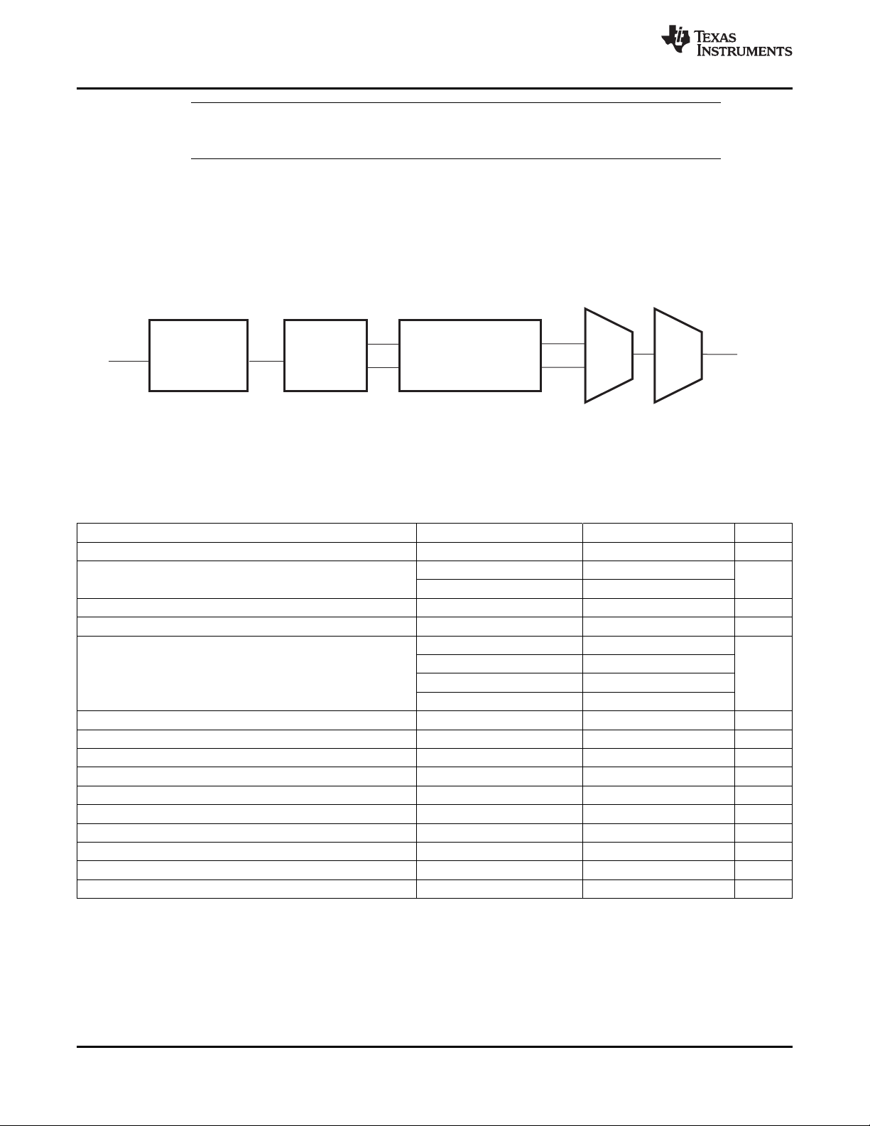
DigitalPGA
gain=0dB
AnalogPGA
gain=0dB
Amp
0dB
DAC
1.35VPP
0dBFs
USB
Amp
–0.6dB
037-052
TPS65930/TPS65920
SWCS037G–MAY 2008– REVISED APRIL 2011
For other component values, see Table 14-1.
Example of ferrite: BLM 18BD221SN1.
6.1.3 Carkit Output
The USB-CEA carkit uses the DP/DM pad to output audio signals (see the CEA-936–Mini-USB Analog
Carkit specification).
Figure 6-4 shows the carkit output downlink full path characteristics for audio and USB.
Figure 6-4. Carkit Output Downlink Path Characteristics
Table 6-3 lists the USB-CEA carkit audio downlink electrical characteristics.
www.ti.com
NOTE
Table 6-3. USB-CEA Carkit Audio Downlink Electrical Characteristics
Parameter Conditions Min Typ Max Unit
Output load USB-CEA (DP/DM) 20 kΩ
Gain range
Absolute gain error At 1 kHz –1 1 dB
Peak-to-peak differential output voltage (0 dBFs) Gain = 0 dB 1.5 V
Total harmonic distortion At 0 dBFs –80 –75 dB
THD+N (20 Hz to 20 kHz, A-weighted) At 0 dBFs 60 dB
Idle channel noise (20 Hz to 20 kHz, A-weighted) Default gain
Output PSRR 20 Hz to 20 kHz 60 dB
Supply voltage (Vintana1) 1.5 V
Common mode output voltage for USB-CEA 1.3 1.35 1.4 V
Isolation between D+/D– during audio mode (20 Hz to 20 kHz) 60 dB
Crosstalk between right and left channels USB-CEA stereo –90 dB
Crosstalk RX/Tx (1 VPPoutput) USB-CEA mono/stereo –60 dB
Signal noise ratio (20 Hz to 20 kHz, A-weighted) At 0 dBFs 60 dB
Phone speaker amplifier output impedance at 1 kHz USB-CEA (DP/DM) 200 Ω
(1) Audio digital filter = –62 to 0 dB (1-dB steps) and 0 to 12 dB (6-dB steps)
(2) The default gain setting assumes the ARXPGA has 0-dB gain setting (volume control) and output driver at 0.6-dB gain setting.
(1)
Voice digital filter = –36 to 12 dB (1-dB steps)
ARXPGA (volume control) = –24 to 12 dB (2-dB steps)
Output driver (USB-CEA) = –1 dB
Audio path –92 30 dB
Voice path –66 30
At –6 dBFs –74 –69
At –20 dBFs –70 –65
At –60 dBFs –30 –25
(2)
–90 –85 dB
PP
58 Audio/Voice Module (TPS65930 Device Only) Copyright © 2008–2011, Texas Instruments Incorporated
Submit Documentation Feedback
focus.ti.com: TPS65930/TPS65920
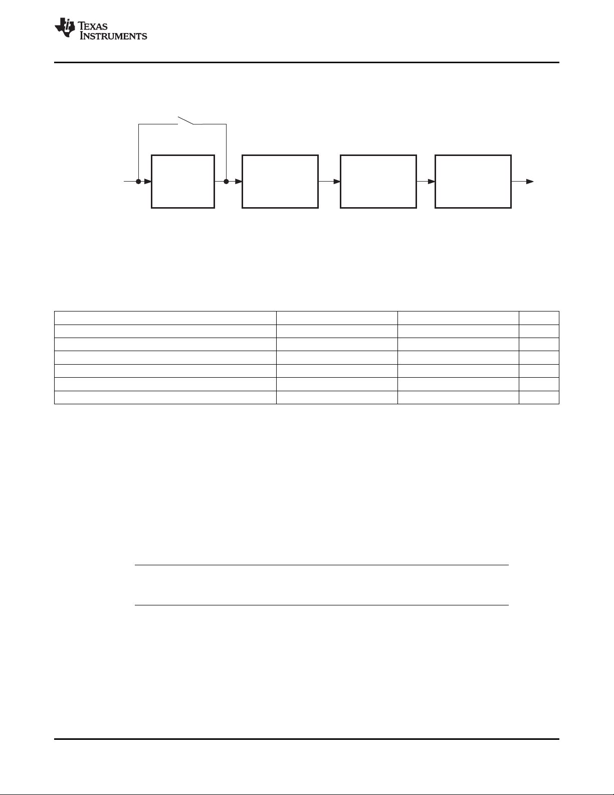
Low-pass
Filter
Digital
modulator
Randomizer
High-pass
filter
Audiointerface
DAC
037-051
TPS65930/TPS65920
www.ti.com
SWCS037G–MAY 2008– REVISED APRIL 2011
6.1.4 Digital Audio Filter Module
Figure 6-5 shows the digital audio filter downlink full path characteristics for the audio interface.
Figure 6-5. Digital Audio Filter Downlink Path Characteristics
The HPF can be bypassed. It is controlled by the MISC_SET_2 ARX_HPF_BYP bit set to address 0x49.
Table 6-4 lists the audio filter frequency responses relative to reference gain at 1 kHz.
Table 6-4. Digital Audio Filter RX Electrical Characteristics
Parameter Conditions Min Typ Max Unit
Passband 0.42 F
S
S
(1)
(1)
to 0.8F
–0.25 0.1 0.25 dB
(1)
S
60 75 dB
(1)
S
Passband ripple 0 to 0.42F
Stopband 0.6 F
Stopband attenuation F = 0.6F
Group delay 15.8/F
Linear phase –1.4 1.4 °
(1) FSis the sampling frequency (8, 11.025, 12, 16, 22.05, 24, 32, 44.1, or 48 kHz).
S
S
μs
6.1.5 Boost Stage
The boost effect adds emphasis to low frequencies. It compensates for a HPF created by the capacitor
resistor (CR) filter of the headset (in ac-coupling configuration).
There are four modes. Three effects are available, with slightly different frequency responses, and the
fourth setting disables the boost effect:
• Boost effect 1
• Boost effect 2
• Boost effect 3
• Flat equalization: The boost effect is in bypass mode.
Boost effect modes are defined in Table 6-5.
Table 6-5 and Table 6-6 include the typical values according to the frequency response versus input
frequency and FSfrequency.
NOTE
Copyright © 2008–2011, Texas Instruments Incorporated Audio/Voice Module (TPS65930 Device Only) 59
Submit Documentation Feedback
focus.ti.com: TPS65930/TPS65920
TPS65930/TPS65920
SWCS037G–MAY 2008– REVISED APRIL 2011
Table 6-5. Boost Electrical Characteristics Versus FSFrequency (FS≤ 22.05 kHz)
Frequency
(Hz)
10 4.51 5.13 5.62 5.10 5.51 5.80 5.22 5.58 5.83 5.54 5.77 5.92 5.76 5.89 5.97
12 4.08 4.83 5.46 4.80 5.32 5.71 4.95 5.41 5.76 5.36 5.66 5.87 5.65 5.83 5.94
15.2 3.43 4.32 5.18 4.28 4.97 5.54 4.47 5.11 5.61 5.03 5.47 5.79 5.45 5.71 5.90
18.2 2.91 3.86 4.89 3.82 4.63 5.36 4.04 4.80 5.45 4.71 5.26 5.69 5.24 5.59 5.84
20.5 2.56 3.53 4.65 3.49 4.37 5.21 3.72 4.56 5.32 4.45 5.09 5.60 5.06 5.49 5.79
29.4 1.62 2.49 3.78 2.45 3.42 4.57 2.68 3.74 4.73 3.51 4.39 5.24 4.35 5.02 5.59
39.7 1.05 1.71 2.93 1.67 2.55 3.84 1.88 2.80 4.06 2.66 3.63 4.72 3.67 4.45 5.27
50.4 0.71 1.20 2.26 1.17 1.91 3.17 1.33 2.13 3.41 2.01 2.95 4.19 2.89 3.85 4.88
60.3 0.51 0.92 1.79 0.89 1.49 2.65 1.00 1.68 2.89 1.57 2.43 3.72 2.39 3.35 4.52
76.7 0.32 0.61 1.26 0.59 1.05 1.99 0.69 1.18 2.22 1.11 1.79 3.04 1.76 2.66 3.94
97.5 0.20 0.39 0.87 0.38 0.70 1.43 0.44 0.79 1.62 0.75 1.27 2.36 1.24 2.00 3.28
131.5 0.12 0.21 0.50 0.20 0.39 0.88 0.25 0.47 1.02 0.42 0.78 1.59 0.75 1.30 2.41
157 0.08 0.15 0.36 0.15 0.28 0.65 0.17 0.33 0.75 0.31 0.57 1.22 0.55 0.99 1.93
200 0.05 0.09 0.22 0.09 0.17 0.41 0.11 0.21 0.49 0.19 0.37 0.82 0.36 0.66 1.38
240 0.03 0.06 0.15 0.06 0.12 0.29 0.07 0.14 0.35 0.14 0.26 0.60 0.25 0.48 1.04
304 0.02 0.04 0.09 0.04 0.07 0.18 0.04 0.09 0.22 0.08 0.16 0.38 0.16 0.30 0.70
463 0.00 0.01 0.03 0.01 0.03 0.07 0.02 0.04 0.09 0.03 0.07 0.17 0.07 0.13 0.32
704 0.00 0.00 0.01 0.00 0.01 0.03 0.01 0.01 0.03 0.01 0.03 0.07 0.03 0.06 0.14
1008 0.00 0.00 0.00 0.00 0.00 0.01 0.00 0.00 0.01 0.00 0.01 0.03 0.01 0.02 0.06
1444 0.00 0.00 0.00 0.00 0.00 0.00 0.00 0.00 0.00 0.00 0.00 0.00 0.00 0.01 0.02
2070 0.00 0.00 0.00 0.00 0.00 0.00 0.00 0.00 0.00 0.00 0.00 0.00 0.00 0.00 0.01
3770 0.00 0.00 0.00 0.00 0.00 0.00 0.00 0.00 0.00 0.00 0.00 0.00 0.00 0.00 0.00
FS= 8 kHz FS= 11.025 kHz FS= 12 kHz FS= 16 kHz FS= 22.05 kHz
1 2 3 1 2 3 1 2 3 1 2 3 1 2 3
www.ti.com
Unit
dB
Table 6-6. Boost Electrical Characteristics Versus FSFrequency (FS≥ 24 kHz)
Frequency
(Hz)
10 5.79 5.90 5.97 5.89 5.89 5.99 5.95 5.98 6.04 5.96 5.99 6.01 5.71 5.83 5.90
12 5.70 5.85 5.95 5.84 5.84 5.98 5.92 5.97 6.03 5.94 5.98 6.00 5.54 5.68 5.81
15.2 5.53 5.76 5.91 5.73 5.73 5.96 5.87 5.94 6.02 5.89 5.95 5.99 5.40 5.57 5.73
18.2 5.35 5.65 5.87 5.62 5.62 5.93 5.80 5.90 6.00 5.83 5.93 5.98 5.28 5.48 5.68
20.5 5.19 5.56 5.83 5.52 5.52 5.91 5.74 5.87 5.99 5.78 5.90 5.97 5.19 5.42 5.64
29.4 4.55 5.18 5.64 5.10 5.07 5.79 5.51 5.75 5.94 5.57 5.79 5.92 4.87 5.18 5.48
39.7 3.81 4.62 5.37 4.52 4.52 5.64 5.12 5.53 5.85 5.26 5.59 5.84 4.47 4.91 5.30
50.4 3.14 4.06 5.02 3.94 3.95 5.43 4.69 5.27 5.72 4.88 5.37 5.73 4.08 4.63 5.11
60.3 2.62 3.51 4.69 3.46 3.54 5.21 4.30 5.00 5.59 4.49 5.13 5.62 3.72 4.37 4.95
76.7 1.97 2.90 4.15 2.76 2.76 4.78 3.68 4.52 5.34 3.91 4.70 5.40 3.18 3.92 4.67
97.5 1.41 2.22 3.51 2.10 2.09 4.27 2.99 3.94 4.99 3.24 4.15 5.07 2.59 3.41 4.33
131.5 0.88 1.49 2.65 1.40 1.40 3.49 2.15 3.10 4.35 2.38 3.35 4.51 1.86 2.69 3.75
157 0.65 1.13 2.15 1.04 1.04 2.96 1.70 2.58 3.90 1.90 2.82 4.08 1.47 2.24 3.35
200 0.41 0.76 1.55 0.70 0.70 2.28 1.19 1.93 3.23 1.35 2.15 3.44 1.03 1.68 2.77
240 0.30 0.55 1.18 0.50 0.50 1.81 0.89 1.51 2.71 1.02 1.70 2.92 0.77 1.31 2.32
304 0.18 0.35 0.80 0.33 0.32 1.27 0.58 1.04 2.05 0.68 1.19 2.24 0.51 0.90 1.75
463 0.08 0.16 0.37 0.14 0.14 0.64 0.27 0.50 1.12 0.31 0.58 1.25 0.23 0.43 0.95
704 0.03 0.06 0.16 0.06 0.06 0.29 0.12 0.23 0.56 0.14 0.27 0.62 0.10 0.20 0.46
1008 0.01 0.03 0.07 0.03 0.02 0.14 0.06 0.11 0.30 0.06 0.13 0.31 0.05 0.10 0.23
1444 0.00 0.01 0.03 0.01 0.01 0.06 0.03 0.05 0.16 0.03 0.06 0.15 0.02 0.05 0.11
2070 0.00 0.00 0.01 0.00 0.00 0.02 0.01 0.02 0.09 0.01 0.03 0.07 0.01 0.02 0.05
3770 0.00 0.00 0.00 0.00 0.00 0.00 0.00 0.00 0.04 0.00 0.00 0.01 0.00 0.00 0.01
FS= 24 kHz FS= 32 kHz FS= 44.1 kHz FS= 48 kHz FS= 96 kHz
1 2 3 1 2 3 1 2 3 1 2 3 1 2 3
Unit
dB
60 Audio/Voice Module (TPS65930 Device Only) Copyright © 2008–2011, Texas Instruments Incorporated
Submit Documentation Feedback
focus.ti.com: TPS65930/TPS65920
TPS65930/TPS65920
www.ti.com
SWCS037G–MAY 2008– REVISED APRIL 2011
6.2 Audio Uplink (TX) Module
The audio uplink path includes two input amplification stages:
• MIC_MAIN_P, MIC_MAIN_M (differential main handset input)
• AUXR (common terminal: single-ended auxiliary)
NOTE
If two audio inputs are needed, and mic bias is not needed, the AUXR input can be used
with MIC_MAIN to provide the two inputs.
6.2.1 Microphone Bias Module
A bias generator provides an external voltage of 2.2 V to bias the analog microphones (MICBIAS1
terminal). The typical output current is 1 mA.
6.2.1.1 Analog Microphone Bias Module Characteristics
Table 6-7 lists the characteristics of the analog microphone bias module.
Table 6-7. Analog Microphone Bias Module Characteristics With Bias Resistor
Parameter Test Conditions Min Typ Max Unit
Bias voltage 2.15 2.2 2.25 V
Load current 1 mA
Output noise P-weighted 20 Hz to 6.6 kHz 1.8 μV
External capacitor 0 200 pF
Internal resistance 50 60 70 kΩ
RMS
NOTE
If the external capacitor is higher than 200 pF, the analog microphone bias becomes
unstable. To stabilize it, add a serial resistor.
Table 6-8 lists the characteristics of the analog microphone bias module with a bias resistor.
Table 6-8. Analog Microphone Bias Module Characteristics With Bias Resistor
Parameter Test Conditions Min Typ Max Unit
CB< 200 pF 0
R
SB
RB+ R
SB
CB= 100 pF 300 Ω
CB= 1 μF 500
2.2 to 2.7 kΩ
Copyright © 2008–2011, Texas Instruments Incorporated Audio/Voice Module (TPS65930 Device Only) 61
Submit Documentation Feedback
focus.ti.com: TPS65930/TPS65920
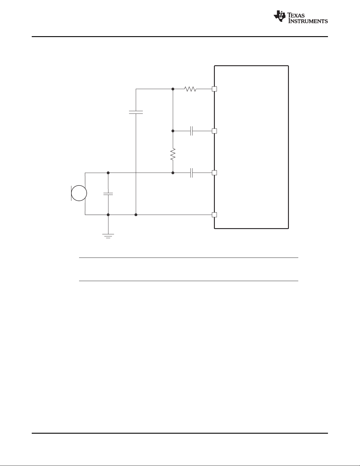
Device
Onboard
MICBIAS.GND
MIC.MAIN.P
MICBIAS1.OUT
C
MM.O
R
MM.O
C
MM.B
C
MM.M
MIC.MAIN.M
R
MM.MP
C
MM.P
037-005
TPS65930/TPS65920
SWCS037G–MAY 2008– REVISED APRIL 2011
Figure 6-6 and Figure 6-7 show the external components and application schematics for the analog
microphone.
www.ti.com
Figure 6-6. Analog Microphone Pseudodifferential
For other component values, see Table 14-1.
NOTE
62 Audio/Voice Module (TPS65930 Device Only) Copyright © 2008–2011, Texas Instruments Incorporated
Submit Documentation Feedback
focus.ti.com: TPS65930/TPS65920
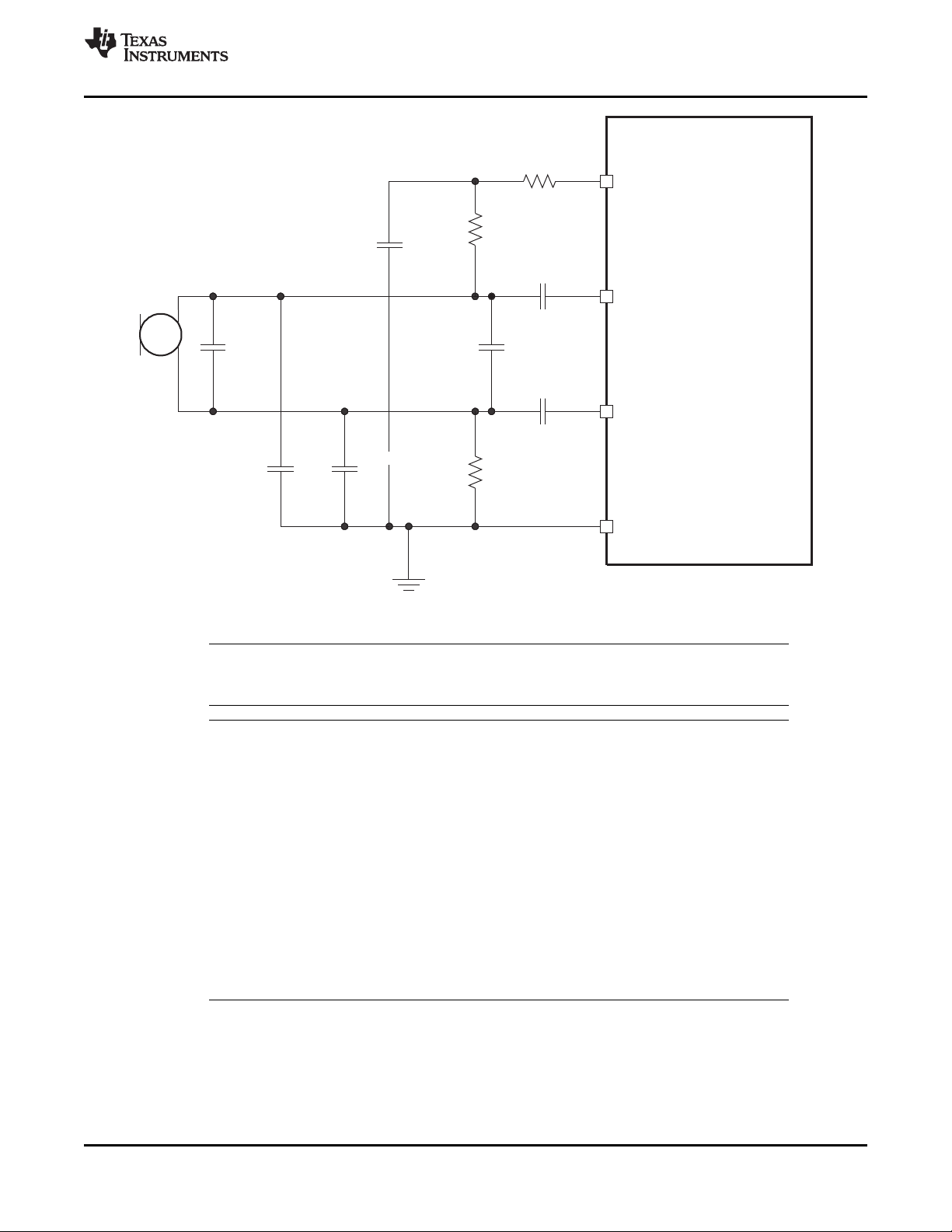
DeviceONBOARD
MICBIAS.GND
MIC.MAIN.P
MICBIAS1.OUT
R
MM.BP
C
MM.B
MIC.MAIN.M
47pF
Closeto
Device
Closeto
Device
037-006
C
MM.P
C
MM.PM
C
MM.M
R /2
MM.GM
C
MM.GM
C
MM.GP
R /2
MM.GM
TPS65930/TPS65920
www.ti.com
SWCS037G–MAY 2008– REVISED APRIL 2011
Figure 6-7. Analog Microphone Differential
For other component values, see Table 14-1.
To improve the rejection, ensure that MICBIAS_GND is as clean as possible. This ground
must be shared with AGND of the TPS65920 or TPS65930 device and must not share with
AVSS4, which is the ground used by RX class AB output stages.
In differential mode, adding a low-pass filter (made by RSBand CB) is highly recommended if
coupling between RX output stages and the microphone is too high (and not enough
attenuation by the echo cancellation algorithm). The coupling can come from:
• The internal TPS65920/TPS65930 coupling between MICBIAS.OUT voltage and RX
output stages
• Coupling noise between MICBIAS.GND and AVSS4
In pseudodifferential mode, the dynamic resistance of the microphone improves the rejection
versus MICBIAS.OUT:
PSRR = 20*log((RB+ R
Dyn_mic
)/RB).
6.2.1.2 Silicon Microphone Module Characteristics
Based on silicon micro-electrical-mechanical system (MEMS) technology, the new microphone achieves
the same acoustic and electrical properties as conventional microphones, but is more rugged and exhibits
higher heat resistance. These properties offer designers of a wide range of products greater flexibility and
new opportunities to integrate microphones.
NOTE
NOTE
Copyright © 2008–2011, Texas Instruments Incorporated Audio/Voice Module (TPS65930 Device Only) 63
Submit Documentation Feedback
focus.ti.com: TPS65930/TPS65920

Device
Onboard
MICBIAS.GND
MIC.MAIN.P
MICBIAS1.OUT
R
SM
MIC.MAIN.M
4 1
3 2
Power Output
GND GND
1 kW
Optional
dependingon
dynamicofMIC
SiliconMIC
SPM0204HE5-PB
(SPM0102ND3-C)
037-007
C
SM
C
SM.P
C
SM.PG
C
SM.M
TPS65930/TPS65920
SWCS037G–MAY 2008– REVISED APRIL 2011
www.ti.com
The silicon microphone is the integration of mechanical elements and electronics on a common silicon
substrate through microfabrication technology.
The complementary metal oxide semiconductor (CMOS) MEMS microphone is more like an analog IC
than a classical microphone, or electric condenser microphone (ECM). It is powered as an IC with a direct
connection to the power supply. The on-chip isolation between the power input and the rest of the system
adds power supply rejection (PSR) to the component. This makes the CMOS MEMS microphone
inherently more immune to power supply noise than an ECM and eliminates the need for additional
filtering circuitry to keep the power supply line clean.
Table 6-9 lists the characteristics of the silicon microphone module.
Table 6-9. Silicon Microphone Module Characteristics
Parameter Test Conditions Min Typ Max Unit
Bias voltage 2.2 V
Load current 1 mA
Output noise P-weighted 20 Hz to 6.6 kHz 1.8 μV
Figure 6-8 is a schematic for the silicon microphone.
RMS
Figure 6-8. Silicon Microphone
NOTE
For other component values, see Table 14-1.
64 Audio/Voice Module (TPS65930 Device Only) Copyright © 2008–2011, Texas Instruments Incorporated
Submit Documentation Feedback
focus.ti.com: TPS65930/TPS65920

Onboard Chip
C
AUXR
C
AUXR.M
AUXR
037-008
DigitalPGA
gain=0to31dB
Amp
0to30dB
ADC
037-050
TPS65930/TPS65920
www.ti.com
6.2.2 FM Radio/Auxiliary Input
The auxiliary input AUXR/FMR can be used as FM radio input. The amplification stage output is
connected to the ADC input. The FM radio input can also be output through an audio output stage.
6.2.2.1 External Components
Figure 6-9 shows the external components on the auxiliary input.
SWCS037G–MAY 2008– REVISED APRIL 2011
Figure 6-9. Audio Auxiliary Input
NOTE
For other component values, see Table 14-1.
6.2.3 Uplink Characteristics
Figure 6-10 shows the uplink amplifier. Table 6-10 lists the uplink characteristics.
Parameter Test Conditions Min Typ Max Unit
Speech delay Voice path 0.5 ms
Gain range
Absolute gain 0 dBFs at 1.02 kHz –1 1 dB
Peak-to-peak differential input voltage (0 dBFs) For differential input 1.5 V
(1)
Figure 6-10. Uplink Amplifier
Table 6-10. Uplink Characteristics
0 61 dB
0 dB gain setting
PP
(1) Gain range is defined by: Preamplifier = 0 to 30 dB; Filter = 0 to 31 dB (1-dB steps)
Copyright © 2008–2011, Texas Instruments Incorporated Audio/Voice Module (TPS65930 Device Only) 65
Submit Documentation Feedback
focus.ti.com: TPS65930/TPS65920

TPS65930/TPS65920
SWCS037G–MAY 2008– REVISED APRIL 2011
www.ti.com
Table 6-10. Uplink Characteristics (continued)
Parameter Test Conditions Min Typ Max Unit
Peak-to-peak single-ended input voltage (0 dBFs) For single-ended input 1.5 V
Input impedance
Total harmonic distortion (sine wave at 1.02 kHz) At –1 dBFs –80 –75 dB
Idle channel noise 20 Hz to 20 kHz, A-weighted, gain = 0 dB –85 –78 dBFs
Crosstalk A/D to D/A Gain = 0 dB –80 dB
Crosstalk path between two microphones –70 dB
Intermodulation distortion 2-tone method –60 dB
(2) Impedance varies in the specified range with gain selection.
(2)
0 dB gain setting
40k 70k Ω
At –6 dBFs –74 –69
At –10 dBFs –70 –65
At –20 dBFs –60 –55
At –60 dBFs –20 –15
16 kHz: < 20 Hz to 7 kHz, gain = 0 dB –90
8 kHz: P-weighted voice, gain = 18 dB –87
16 kHz: < 20 Hz to 7 kHz, gain = 18 dB –82
6.2.4 Microphone Amplification Stage
The microphone amplification stages perform the single-to-differential conversion for single-ended inputs.
Two programmable gains from 0 dB to 30 dB can be set:
• Automatic level control for main microphone input. The gain step is 1 dB.
• Level control by register for line-in or carkit input. The gain step is 6 dB.
PP
The amplification stage outputs are connected to the ADC input (ADC left and right).
66 Audio/Voice Module (TPS65930 Device Only) Copyright © 2008–2011, Texas Instruments Incorporated
Submit Documentation Feedback
focus.ti.com: TPS65930/TPS65920

DigitalPGA
gain=0to31dB
Amp
0to
30dB
ADC
Amp
CEA
–1.02dB
037-009
TPS65930/TPS65920
www.ti.com
SWCS037G–MAY 2008– REVISED APRIL 2011
6.2.5 Carkit Input
The USB-CEA carkit uses the DP pad to input the audio signal.
Figure 6-11 shows the uplink carkit full path uplink characteristics for audio and USB.
Figure 6-11. Carkit Input Uplink Path Characteristics
Table 6-11 lists the USB-CEA carkit audio electrical characteristics.
Table 6-11. USB-CEA Carkit Audio Uplink Electrical Characteristics
Parameter Test Conditions Min Typ Max Unit
Gain range
Absolute gain, 0 dBFs at 1.02 kHz
Speech delay Voice path 0.5 ms
Input common mode voltage
Phone microphone amplifier input impedance at 1 kHz USB-CEA 8 120 kΩ
Peak-to-peak single-ended input voltage (0 dBFs) Default setting 1.414 V
Total harmonic distortion (sine wave at 1 kHz), default gain setting At –1 dBFs –74 –60 dB
THD+N (20 Hz to 20 kHz, A-weighted) At 0 dBFs 60 dB
Signal noise ratio (20 Hz to 20 kHz, A-weighted) At 0 dBFs 60 dB
Idle channel noise (20 Hz to 20 kHz, A-weighted), default gain USB-CEA –77
setting
Output PSRR (20 Hz to 20 kHz, A-weighted) USB-CEA 50 dB
(1) Gain range is defined by: CEA amplifier = 0.56 to –1.02 dB; Preamplifier = 0 to 30 dB; Filter = 0 to 31 dB (1-dB steps).
(2) The CEA default gain setting assumes 0 dB on the preamplifier, 1 dB on digital filter, and CEA amplifier at –1.02 dB.
(3) Full-scale input voltage is 1 V minimum.
(1)
(1) (2)
(3)
USB-CEA default gain setting –1.5 1.5 dB
USB-CEA 1.3 1.9 V
At –6 dBFs
At –10 dBFs
At –20 dBFs
At –60 dBFs
–1 60 dB
dBFs
PP
Copyright © 2008–2011, Texas Instruments Incorporated Audio/Voice Module (TPS65930 Device Only) 67
Submit Documentation Feedback
focus.ti.com: TPS65930/TPS65920

Error
cancellation
A/Doutput
Audio
interface
SINCfilter
differentiator
4thorder
SINCfilter
integrator
4thorder
1storderhigh-
passfilter
Low-pass
filter
037-017
TPS65930/TPS65920
SWCS037G–MAY 2008– REVISED APRIL 2011
www.ti.com
6.2.6 Digital Audio Filter Module
Figure 6-12 shows the digital audio filter uplink full path characteristics for the audio interface.
Figure 6-12. Digital Audio Filter Uplink Path Characteristics
The high-pass filter (HPF) can be bypassed. It is controlled by the MISC_SET_2 ATX_HPF_BYP bit set to
address 0x49.
Table 6-12 lists the audio filter frequency responses relative to reference gain at 1 kHz.
Table 6-12. Digital Audio Filter TX Electrical Characteristics
Parameter Test Conditions Min Typ Max Unit
Passband 0.0005 0.42 F
Passband gain In region 0.0005*FSto 0.42*F
Stopband 0.6 F
Stopband attenuation In region 0.6*FSto 1*F
Group delay 15.8/F
(1) FSis the sampling frequency (8, 11.025, 12, 16, 22.05, 24, 32, 44.1, or 48 kHz).
S
(1)
S
(1)
–0.25 0.25 dB
60 dB
S
S
S
μs
68 Audio/Voice Module (TPS65930 Device Only) Copyright © 2008–2011, Texas Instruments Incorporated
Submit Documentation Feedback
focus.ti.com: TPS65930/TPS65920

Freeheadset
OMAP
(LINK)
ULPI
UART control
Phoneconnector
(USB)
ADCinputs
(optional)
Audioaccessory
USBOTGdevice
PC
Carkit
Device
USBPHY
037-011
TPS65930/TPS65920
www.ti.com
7 USB Transceiver
7.1 USB Transceiver
The TPS65920/TPS65930 device includes a USB OTG transceiver with the CEA carkit interface that
supports USB 480 Mbps HS, 12 Mbps full-speed (FS), and USB 1.5 Mbps low-speed (LS) through a 4-pin
ULPI.
The carkit block ensures the interface between the phone and a carkit device. The TPS65920/TPS65930
USB supports the CEA carkit standard.
Figure 7-1 is a block diagram of the USB 2.0 physical layer (PHY).
SWCS037G–MAY 2008– REVISED APRIL 2011
Figure 7-1. USB 2.0 PHY Block Diagram
7.1.1 Features
The device has a USB OTG carkit transceiver that allows system implementation that complies with the
following specifications:
• Universal Serial Bus 2.0 Specification
• On-The-Go Supplement to the USB 2.0 Specification
• CEA-2011: OTG Transceiver Interface Specification
• CEA-936A: Mini-USB Analog Carkit Specification
• UTMI+ Low Pin Interface Specification
The features of the individual specifications are:
• Universal Serial Bus 2.0 Specification (hereafter referred to as the USB 2.0 specification):
– 5-V-tolerant data line at HS/FS, FS-only, and LS-only transmission rates
– 7-V-tolerant video bus (VBUS) line
– Integrated data line serial termination resistors (factory-trimmed)
– Integrated data line pullup and pulldown resistors
– On-chip 480-MHz phase-locked loop (PLL) from the internal system clock (19.2, 26, and 38.4 MHz)
– Synchronization (SYNC)/end-of-period (EOP) generation and checking
– Data and clock recovery from the USB stream
– Bit-stuffing/unstuffing and error detection
– Resume signaling, wakeup, and suspend detection
– USB 2.0 test modes
• On-The-Go Supplement to the USB 2.0 Specification (hereafter referred to as the OTG supplement to
the USB 2.0 specification):
– 3-pin LS/FS serial mode (DAT_SE0)
– 4-pin LS/FS serial mode (VP_VM)
• CEA-936A: Mini-USB Analog Carkit Interface Specification:
Copyright © 2008–2011, Texas Instruments Incorporated USB Transceiver 69
– 5-pin CEA mini-USB analog carkit interface
Submit Documentation Feedback
focus.ti.com: TPS65930/TPS65920

C P.GN D
DATA7
DATA6
DATA5
DATA4
DATA3/CTSO
DATA2/RTSI
DATA1/TX
DATA0/RX
NXT
DIR
STP
USB2.0
HS-OTG
transceiver
withCEA
carkitinterface
C
VBUS1
VBAT
C
VBUS.FC
C P.CA P P
C P.CA P N
C P.IN
C
VBUS.IN
USBCP
VIN T U S B .1 P 8
C
VINTUSB.1P8
.*
VIN T U S B .1 P 5
C
VINTUSB.1P5
VUSB. 3P1
C
VUSB.3P1
CP.OUT
Hostprocessor
UCLK
GND
VBUS
DM/UART3.TXD
DP/UART3.RXD
ID
C
VBUS2
USB-CEA
carkit
connector
C
VBAT.USB
Device
037-012
TPS65930/TPS65920
SWCS037G–MAY 2008– REVISED APRIL 2011
–
UART signaling
– Audio (mono/stereo) signaling
– UART transactions during audio signaling
– Basic and smart 4-wire/5-wire carkit, chargers, and accessories
– ID CEA resistor comparators
• UTMI+ Low Pin Interface Specification (hereafter referred to as the ULPI specification):
– 12-pin ULPI with 8-pin parallel data for USB signaling and register access
– 60-MHz clock generation
– Register mapping
Figure 7-2 is the USB system application schematic.
www.ti.com
7.1.2 HS USB Port Timing
70 USB Transceiver Copyright © 2008–2011, Texas Instruments Incorporated
The ULPI interface supports an 8-bit data bus and the internal clock mode. The 4-bit data bus and the
external clock mode are not supported.
The HS functional mode supports an operating rate of 480 Mbps.
Table 7-1 and Table 7-2 assume testing over the recommended operating conditions (see Figure 7-3).
For the component values, see Table 14-1.
Figure 7-2. USB System Application Schematic
NOTE
Submit Documentation Feedback
focus.ti.com: TPS65930/TPS65920

UCLK
STP
DIR_&_NXT
DATA[7:0]
Data_OUT Data_IN
HSU0
HSU3
HSU3
HSU6 HSU7
HSU1 HSU1
HSU4
HSU5
HSU2 HSU2
037-049
TPS65930/TPS65920
www.ti.com
The input timing requirements are given by considering a rising or falling time of 1 ns (see Table 7-1).
SWCS037G–MAY 2008– REVISED APRIL 2011
Figure 7-3. HS-USB Interface—Transmit and Receive Modes (ULPI 8-bit)
NOTE
ULPI data [7:0] lines are set to 1 after USB PHY power up, and before the clock signal is
stable.
Table 7-1. HS-USB Interface Timing Requirements
Notation Parameter Min Max Unit
HSU4 t
HSU5 t
HSU6 t
HSU7 t
s(STPV-CLKH)
h(CLKH-STPIV)
s(DATAV-CLKH)
h(CLKH-DATIV)
Setup time, STP valid before UCLK rising 6 ns
edge
Hold time, STP valid after UCLK rising edge 0 ns
Setup time, DATA[0:7] valid before UCLK 6
rising edge
Hold time, DATA[0:7] valid after UCLK rising 0
edge
Table 7-2 lists the HS-USB interface switching requirements.
Table 7-2. HS-USB Interface Switching Requirements
Notation Parameter
HSU0 f
HSU1 t
HSU2
HSU3 t
(1) The capacitive load for output data and control load is 10 pF (rising and falling time is 2 ns).
The capacitive load for the CLK port is 6 pF (rising and falling time is 1 ns).
The HS-USB interface has only one state: the steady state.
p(CLK)
W(CLK)
t
d(CLKH-DIR)
t
d(CLKH-NXTV)
d(CLKH-DATV)
UCLK clock frequency Steady state 58.42 60 61.67 MHz
UCLK duty cycle Steady state 48.3% 50% 51.7%
Delay time, UCLK rising edge to Steady state 0 9
DIR transition
Delay time, UCLK rising edge to Steady state 0 9
NXT transition
Delay time, UCLK rising edge to Steady state 0 9
DATA[0:7] transition
(1)
ns
ns
(1)
Min Typ Max Unit
ns
ns
ns
7.1.3 USB-CEA Carkit Port Timing
This mode allows the link for communication through the USB PHY to a remote carkit in CEA audio + data
during audio (DDA) mode as defined in the CEA-936A specification. In this mode, the ULPI data bus is
redefined as a 2-pin UART interface, which exchanges data through a direct access to the FS/LS analog
transmitter and receiver.
Copyright © 2008–2011, Texas Instruments Incorporated USB Transceiver 71
Submit Documentation Feedback
focus.ti.com: TPS65930/TPS65920

ULPI
DATA0:UART_TX
DATA1:UART_RX
Device
USB-CEA connector
DP/RXD/MIC
DM/TXD/SPKR
037-048
TPS65930/TPS65920
SWCS037G–MAY 2008– REVISED APRIL 2011
UART data are sent and received on the USB D+/D– pads. D+/D– are also used in this mode to carry
audio I/O signals.
Table 7-3 assumes testing over the recommended operating conditions (see the CEA-936A specification).
Table 7-3. USB-CEA Carkit Interface Timing Parameters
t
PH_DP_CON
t
CR_DP_CON
t
PH_DM_CON
t
PH_CMD_DLY
t
PH_MONO_ACK
t
PH_DISC_DET
t
CR_DISC_DET
t
PH_AUD_BIAS
t
CR_AUD_DET
t
CR_UART_DET
t
PH_STLO_DET
t
PH_PLS_POS
t
CR_PLS_NEG
t
DAT_AUD_POL
t
ACC_COL_DET
t
ACC_INT_PW
t
ACC_INT_WAIT
t
ACC_CMD_WAIT
t
PH_INT_PW
t
PH_INT_WAIT
t
PH_CMD_WAIT
t
PH_UART_RPT
t
CR_UART_RSP
t
CR_INT_RPT
f
UART_DFLT
Phone D+ connect time 100 ms
Carkit D+ connect time 150 300 ms
Phone D– connect time 10 ms
Phone command delay 2 ms
Phone mono acknowledge 10 ms
Phone D+ disconnect time 150 ms
Carkit D– disconnect detect 50 150 ms
Phone audio bias 1 ms
Carkit audio detect 400 800 μs
Carkit UART detect (data-during-audio enabled) 700 1200 ns
Phone stereo D+ low detect 30 100 ms
Phone D– interrupt pulse width 200 600 ns
Carkit D+ interrupt pulse width 200 600 ns
Data-during-audio polarity 20 60 ms
Accessory ID collision detect 2 3 ms
Accessory ID interrupt pulse width 200 400 μs
Accessory ID interrupt wait time 10 15 ms
Accessory ID command wait time 0 ms
Phone ID interrupt pulse width 4 8 ms
Phone ID interrupt wait time 4 8 ms
Phone ID command wait time 0 ms
Phone command repeat time 50 ms
Carkit UART response 30 ms
Carkit interrupt repeat time 50 ms
Default UART signaling rate (typical rate) 9600 bps
www.ti.com
Parameter Min Max Unit
72 USB Transceiver Copyright © 2008–2011, Texas Instruments Incorporated
Figure 7-4 shows the USB-CEA carkit UART data flow.
Figure 7-4. USB-CEA Carkit UART Data Flow
Table 7-4 lists the USB-CEA carkit UART timings.
Submit Documentation Feedback
focus.ti.com: TPS65930/TPS65920

UART_TX
DM
DP
UART_RX
CK1 CK2
CK3 CK4
037-047
TPS65930/TPS65920
www.ti.com
SWCS037G–MAY 2008– REVISED APRIL 2011
Table 7-4. USB-CEA Carkit UART Timings
Notation Parameter Min Max Unit
CK1 t
CK2 t
CK3 t
CK4 t
d(UART_TXH-DM)
d(UART_TXL-DM)
d(DPH-UART_RX)
d(DPL-UART_RX)
Delay time, UART_TX rising edge to DM transition 4.0 11 ns
Delay time, UART_TX falling edge to DM transition 4.0 11 ns
Delay time, DP rising edge to UART_RX
transition
Delay time, DP falling edge to UART_RX
transition
At 38.4 MHz 205 234
At 19.2 MHz 310 364
At 38.4 MHz 205 234
At 19.2 MHz 310 364
Figure 7-5 shows the USB-CEA carkit UART timings.
Figure 7-5. USB-CEA Carkit UART Timings
ns
ns
7.1.4 PHY Electrical Characteristics
The PHY is the physical signaling layer of the USB 2.0. It contains the drivers and receivers for physical
data and protocol signaling on the DP and DM lines.
The PHY interfaces with the USB controller through the UTMI.
The transmitters and receivers in the PHY are of two main classes:
• FS and LS transceivers (legacy USB1.x transceivers)
• HS transceivers
To bias the transistors and run the logic, the PHY also contains reference generation circuitry which
consists of:
• A DPLL that does a frequency multiplication to achieve the 480-MHz low-jitter lock necessary for USB,
and the clock required for the switched capacitor resistance block
• A switched capacitor resistance block that replicates an external resistor on chip
Built-in pullup and pulldown resistors are used as part of the protocol signaling.
The PHY also contains circuitry that protects it from an accidental 5-V short on the DP and DM lines and
from 8-kV IEC ESD strikes.
7.1.4.1 HS Differential Receiver
The HS receiver consists of the following blocks:
• A differential input comparator to receive the serial data
• A squelch detector to qualify the received data
• An oversampler-based clock data recovery scheme followed by a nonreturn to zero inverted (NRZI)
decoder, bit unstuffing, and serial-to-parallel converter to generate the UTMI DATAOUT
Table 7-5 lists the characteristics of the HS differential receiver.
Copyright © 2008–2011, Texas Instruments Incorporated USB Transceiver 73
Submit Documentation Feedback
focus.ti.com: TPS65930/TPS65920
TPS65930/TPS65920
SWCS037G–MAY 2008– REVISED APRIL 2011
www.ti.com
Table 7-5. HS Differential Receiver
Parameter Comments Min Typ Max Unit
Input Levels for HS
HS squelch detection threshold V
HS disconnect detection threshold V
HS data signaling common mode voltage V
range
HS differential input sensitivity V
HSSQ
HSDSC
HSCM
DIHS
(Differential signal amplitude) 100 125 150 mV
(Differential signal amplitude) 525 600 625 mV
–50 200 500 mV
(Differential signal amplitude) –100 100 mV
Input Impedance for HS
Internal specification for input capacitance C
Internal C
DP/DM matching C
HSLOAD
HSLOAD
HSLOADM
11 pF
0.2 pF
External Components With the Total Budget Combined (without USB cable load)
External capacitance on DP or DM 2 pF
External series resistance on DP or DM 1 Ω
7.1.4.2 HS Differential Transmitter
The HS transmitter is always operated on the UTMI parallel interface. The parallel data on the interface is
serialized, bit stuffed, NRZI encoded, and transmitted as a dc output current on DP or DM, depending on
the data. Each line has an effective 22.5-Ω load to ground, which generates the voltage levels for
signaling.
A disconnect detector is also part of the HS transmitter. A disconnect on the far end of the cable causes
the impedance seen by the transmitter to double, thereby doubling the differential amplitude seen on the
DP/DM lines.
Table 7-6 lists the characteristics of the HS differential transmitter.
Table 7-6. HS Differential Transmitter
Parameter Comments Min Typ Max Unit
Output Levels for HS
HS TX idle level V
HS TX data signaling high V
HS data signaling low V
Chirp J level V
Chirp K level V
HS TX disconnect threshold V
Rise time t
Fall time t
Driver output resistance Z
HSOI
HSOH
HSOL
CHIRPJ
CHIRPK
DISCOUT
HSR
HSF
HSDRV
Absolute voltage DP/DM – internal/external 45 Ω –10 0 10 mV
Absolute voltage DP/DM – internal/external 45 Ω 360 400 440 mV
–10 0 10 mV
Differential voltage 700 800 1100 mV
Differential voltage –900 –800 –500 mV
Absolute voltage DP/DM – no external 45 Ω 700 mV
Driver Characteristics
(10%–90%) 500 ps
(10%–90%) 500 ps
Also serves as HS termination 40.5 45 49.5 Ω
74 USB Transceiver Copyright © 2008–2011, Texas Instruments Incorporated
Submit Documentation Feedback
focus.ti.com: TPS65930/TPS65920

TPS65930/TPS65920
www.ti.com
SWCS037G–MAY 2008– REVISED APRIL 2011
7.1.4.3 CEA/UART Driver
Table 7-7 lists the characteristics of the CEA/UART driver.
Table 7-7. CEA/UART Driver
Parameter Comments Min Typ Max Unit
UART Driver CEA
Phone UART edge rates t
Serial interface output high V
Serial interface output low V
PH_UART_EDGE
OH_SER
OL_SER
DP_PULLDOWN asserted 1 μs
ISOURCE = 4 mA 2.4 3.3 3.6 V
ISINK = –4 mA 0 0.1 0.4 V
Carkit Pulse Driver
Pulse match tolerance QPLS_MTCH ZCR_SPKR_IN = 60 kΩ at f = 1 kHz 5%
Phone D– interrupt pulse
width
Phone positive pulse voltage V
t
PH_PLS_POS
PH_PLS_POS
ZCR_SPKR_IN = 60 kΩ at f = 1 kHz 200 600 ns
ZCR_SPKR_IN = 60 kΩ at f = 1 kHz 2.8 3.6 V
7.1.4.4 Pullup/Pulldown Resistors
Table 7-8 lists the characteristics of pullup/pulldown resistors.
Table 7-8. Pullup/Pulldown Resistors
Parameter Comments Min Typ Max Unit
Pullup Resistors
Bus pullup resistor on upstream
port (idle bus)
Bus pullup resistor on upstream
port (receiving)
High (floating) V
Phone D+ pullup voltage V
Phone D+/– pulldown Driver outputs unloaded 14.25 18 24.8 kΩ
High (floating) V
Upstream facing port C
OTG device leakage V
Input impedance exclusive of Driver outputs unloaded (waiver from
pullup/pulldown
(1)
(1) Waiver received from usb.org standards committee on ZINP 300kmin specification
R
PUI
R
PUA
IHZ
PH_DP_UP
R
PH_DP_DWN
R
PH_DM_DWN
IHZ
INUB
OTG_DATA_LKG
Z
INP
Bus idle 0.9 1.1 1.575
Bus driven/driver outputs unloaded 1.425 2.2 3.09
Pullups/pulldowns on DP and DM lines 2.7 3.6 V
Driver outputs unloaded 3 3.3 3.6 V
Pulldown Resistors
Pullups/pulldowns on DP and DM lines 2.7 3.6 V
D+/– Data Line
[1.0] 22 75 pF
[2] 0.342 V
USB.ORG Standard Committee)
80 120 kΩ
kΩ
7.1.5 OTG Electrical Characteristics
The OTG block integrates three main functions:
• The USB plug detection function on VBUS and ID
• The ID resistor detection
• The VBUS level detection
Copyright © 2008–2011, Texas Instruments Incorporated USB Transceiver 75
Submit Documentation Feedback
focus.ti.com: TPS65930/TPS65920
TPS65930/TPS65920
SWCS037G–MAY 2008– REVISED APRIL 2011
www.ti.com
7.1.5.1 OTG VBUS Electrical Characteristics
Table 7-9 lists the electrical characteristics of the OTG VBUS.
Table 7-9. OTG VBUS Electrical Characteristics
Parameter Comments Min Typ Max Unit
VBUS Wake-Up Comparator
VBUS wake-up delay DEL
VBUS wake-up threshold V
VBUS_WK_UP
VBUS_WK_UP
0.5 0.6 0.7 V
VBUS Comparators
A-device session valid V
A-device V
valid V
BUS
B-device session end V
B-device session valid V
A_SESS_VLD
A_VBUS_VLD
B_SESS_END
B_SESS_VLD
0.8 1.1 1.4 V
4.4 4.5 4.6 V
0.2 0.5 0.8 V
2.1 2.4 2.7 V
VBUS Line
A-device V
ground not driving V
B-device V
B-device V
B-device V
maximum for OTG-A t
communication
B-device V
minimum for standard host t
connection
input impedance to SRP (V
BUS
SRP pulldown R
BUS
SRP pullup R
BUS
SRP rise time
BUS
SRP rise time
BUS
R
A_BUS_IN
B_SRP_DWN
B_SRP_UP
RISE_SRP_UP_Max
RISE_SRP_UP_Min
pulsing) capable A-device
BUS
BUS
5.25 V/8 mA, pullup voltage = 3 V 0.656 10 kΩ
(5.25 V – 3 V)/8 mA, pullup voltage = 3
V
0.281 1 2 kΩ
0 to 2.1 V with < 13 μF load 36 ms
0.8 to 2.0 V with > 97 μF load 60 ms
VBUS line maximum voltage If VBUS_CHRG bit is low 7 V
15 μs
100 kΩ
7.1.5.2 OTG ID Electrical Characteristics
Table 7-10 lists the electrical characteristics of OTG ID.
Table 7-10. OTG ID Electrical Characteristics
Parameter Comments Min Typ Max Unit
ID Wake-Up Comparator
ID wake-up comparator R
ID_WK_UP
ID Comparators — ID External Resistor Specifications
ID ground comparator R
ID 100k comparators R
ID 200k comparators R
ID 440k comparators R
ID Float comparator R
Phone IDpullup to V
PH_ID_UP
ID_GND
ID_100K
ID_200K
ID_440K
ID_FLOAT
R
PH_ID_UP
Phone IDpullup voltage VPH_ID_UP Connected to VRUSB 2.5 3.2 V
ID line maximum voltage 5.25 V
Wake-up when ID shorted to ground through a
resistor lower than 445 kΩ (±1%)
ID_GND interrupt when ID shorted to ground
through a resistor lower than 10 Ω
ID_100K interrupt when 102 kΩ (1%) resistor
plugged in
ID_200K interrupt when 200 kΩ (1%) resistor
plugged in
ID_440K interrupt when 440 kΩ (1%) resistor
plugged in
ID_FLOAT interrupt when ID shorted to ground
through a resistor higher than 560 kΩ
445 kΩ
0 5 10 Ω
101 102 103 kΩ
198 200 202 kΩ
435 440 445 kΩ
1400 kΩ
ID Line
ID unloaded (VRUSB) 70 200 286 kΩ
76 USB Transceiver Copyright © 2008–2011, Texas Instruments Incorporated
Submit Documentation Feedback
focus.ti.com: TPS65930/TPS65920

TPS65930/TPS65920
www.ti.com
SWCS037G–MAY 2008– REVISED APRIL 2011
Copyright © 2008–2011, Texas Instruments Incorporated USB Transceiver 77
Submit Documentation Feedback
focus.ti.com: TPS65930/TPS65920
TPS65930/TPS65920
SWCS037G–MAY 2008– REVISED APRIL 2011
www.ti.com
8 MADC
8.1 General Description
The TPS65920/TPS65930 device provides the MADC resource to the host processors in the system
(hardware and software conversion modes).
The MADC generates interrupt signals to the host processors. Interrupts are handled primarily by the
MADC internal secondary interrupt handler and secondly at the upper level (outside the MADC) by the
TPS65920/TPS65930 interrupt primary handler.
8.2 MADC Electrical Characteristics
Table 8-1 lists the electrical characteristics of the MADC.
Table 8-1. MADC Electrical Characteristics
Parameter Conditions Min Typ Max Unit
Resolution 10 Bit
ADIN2 input dynamic range for external input 0 2.5 V
MADC voltage reference 1.5 V
ADIN0 differential nonlinearity –1 1 LSB
ADIN0 integral nonlinearity Best fitting –2 2 LSB
Integral nonlinearity for ADIN2
Offset Best fitting –28.5 28.5 mV
Input bias 1 μA
Input capacitor C
Maximum source input resistance Rs (for all 16 100 kΩ
internal or external inputs)
Input current leakage (for all 16 internal or external 1 μA
inputs)
BANK
Best fitting for codes 230 to maximum –2 2 LSB
Best fitting considering offset of 25 LSB –3.75 3.75 LSB
10 pF
78 MADC Copyright © 2008–2011, Texas Instruments Incorporated
Submit Documentation Feedback
focus.ti.com: TPS65930/TPS65920
TPS65930/TPS65920
www.ti.com
SWCS037G–MAY 2008– REVISED APRIL 2011
8.3 Channel Voltage Input Range
Table 8-2 lists the analog input voltage minimum and maximum values.
Table 8-2. Analog Input Voltage Range
Channel Min Typ Max Unit Prescaler
ADIN0: General-purpose input 0 1.5 V DC current source for battery identification through external
ADIN2: General-purpose input
(1) General-purpose inputs must be tied to ground when TPS65920/TPS65930 internal power supplies (VINTANA1 and VINTANA2) are off.
(1)
0 2.5 V Prescaler in the MADC to be in range 0 to >1.5 V
No prescaler
resistor (10 μA typical)
8.3.1 Sequence Conversion Time (Real-Time or Nonaborted Asynchronous)
Table 8-3 lists the sequence conversion timing characteristics.
Table 8-3. Sequence Conversion Timing Characteristics
Parameter Comments Min Typ Max Unit
F Running frequency 1 MHz
T = 1/F Clock period 1 μs
N Number of analog inputs to convert in a single sequence 0 2
Tstart SW1, SW2, or USB asynchronous request or real-time STARTADC
Tsettling time Settling time to wait before sampling a stable analog input (capacitor 5 12 20 μs
Tstartsar The successive approximation registers ADC start time 1 μs
Tadc time The successive approximation registers ADC conversion time 10 μs
Tcapture time Tcapture time is the conversion result capture time. 2 μs
Tstop 1 2 μs
Full-conversion One channel (N = 1)
sequence time
Conversion sequence
time
STARTADC pulse
duration
(1) Total sequence conversion time general formula: Tstart+N*(1+Tsettling+Tadc+Tcapture) +Tstop
request
bank charge time)
Tsettling is calculated from the max((Rs + Ron)*Cbank) of the two
possible input sources (internal or external). Ron is the resistance of the
selection analog input switches (5 kΩ). This time is
software-programmable by the open-core protocol (OCP) register.
(1)
Both channels
Without Tstart and Tstop: One channel (N = 1)
Without Tstart and Tstop: Both channels
STARTADC period is T. 0.33 24 μs
(1)
(1)
(1)
3 4 μs
22 39
352 624
18 33
288 528
μs
μs
Copyright © 2008–2011, Texas Instruments Incorporated MADC 79
Submit Documentation Feedback
focus.ti.com: TPS65930/TPS65920

T oneconversion
Tstart
Tsettling Tadc
Tstartsar
Tstop
Tcapture
madc_clk
Busy
mux_sel_lowv[3:0]
Acquire_lowv
start_sar_lowv
out_lowv[9:0]
channelN
resultregister
channelNselected
newchannelNvalue
newvalueoldvalue
channelXvalue
037-046
TPS65930/TPS65920
SWCS037G–MAY 2008– REVISED APRIL 2011
Table 8-3 is illustrated in Figure 8-1, which is a conversion sequence general timing diagram. The Busy
parameter indicates that a conversion sequence is running, and the channel N result register parameter
corresponds to the result register of the RT/GP selected channel.
www.ti.com
Figure 8-1. Conversion Sequence General Timing Diagram
80 MADC Copyright © 2008–2011, Texas Instruments Incorporated
Submit Documentation Feedback
focus.ti.com: TPS65930/TPS65920

LEDSYNC
LEDGND
LEDB
BATT
Device
*16...
BATT
120 W
160 W
037-045
TPS65930/TPS65920
www.ti.com
9 LED Drivers
9.1 General Description
Two arrays of parallel LEDs are driven (dedicated for the phone light). The parallel LEDs are supplied by
VBAT, and the external resistor value is given for each LED. The TPS65920/TPS65930 device supports
two open-drain LED drivers for the keypad backlight, having drain connections tolerant of the main battery
voltage.
Figure 9-1 is the LED driver block diagram. Table 9-1 lists the electrical characteristics of the LED driver.
SWCS037G–MAY 2008– REVISED APRIL 2011
Figure 9-1. LED Driver Block Diagram
NOTE
For the component values, see Table 14-1.
Table 9-1. LED Driver Electrical Characteristics
Parameter Conditions Min Typ Max Unit
SW On resistance Ω
IO= 160 mA 3 4
IO= 60 mA 10 12
Copyright © 2008–2011, Texas Instruments Incorporated LED Drivers 81
Submit Documentation Feedback
focus.ti.com: TPS65930/TPS65920

Device
Keyboardcontroller
kbd_r_0
kbd_c_0
VCC
Internal
pullup
kbd_r_1
kbd_r_2
kbd_r_3
kbd_r_4
kbd_r_5
kbd_c_1
kbd_c_2
kbd_c_3
kbd_c_4
kbd_c_5
6x6
Keyboardmatrix
037-014
TPS65930/TPS65920
SWCS037G–MAY 2008– REVISED APRIL 2011
10 Keyboard
10.1 Keyboard Connection
The keyboard is connected to the chip using:
• KBR (5 :0) input pins for row lines
• KBC (5 :0) output pins for column lines
Figure 10-1 shows the keyboard connection.
www.ti.com
82 Keyboard Copyright © 2008–2011, Texas Instruments Incorporated
When a key button of the keyboard matrix is pressed, the corresponding row and column lines are shorted
together. To allow key press detection, all input pins (KBR) are pulled up to VCCand all output pins (KBC)
Figure 10-1. Keyboard Connection
are driven to a low level.
Any action on a button generates an interrupt to the sequencer.
The decoding sequence is written to allow detection of simultaneous press actions on several key buttons.
The keyboard interface can be used with a smaller keyboard area than 6 × 6. To use a 3 × 3 keyboard,
KBR(4) and KBR(5) must be tied high to prevent any scanning process distribution.
Submit Documentation Feedback
focus.ti.com: TPS65930/TPS65920

Device
32KXOUT
OR
HFCLKIN
32KCLKOUT
HFCLKOUT
32KXIN
OR
OR
32kHz
030-002
TPS65930/TPS65920
www.ti.com
11 Clock Specifications
The TPS65920/TPS65930 device includes several I/O clock pins. The TPS65920/TPS65930 device has
two sources of high-stability clock signals: the external high-frequency clock (HFCLKIN) input and an
onboard 32-kHz oscillator (an external 32-kHz signal can be provided). Figure 11-1 is the clock overview.
SWCS037G–MAY 2008– REVISED APRIL 2011
11.1 Clock Features
The TPS65920/TPS65930 device accepts two sources of high-stability clock signals:
• 32KXIN/32KXOUT: Onboard 32-kHz crystal oscillator (an external 32-kHz input clock can be provided)
• HFCLKIN: External high-frequency clock (19.2, 26, or 38.4 MHz).
The TPS65920/TPS65930 device can provide:
• 32KCLKOUT digital output clock
• HFCLKOUT digital output clock with the same frequency as the HFCLKIN input clock
Figure 11-1. Clock Overview
Copyright © 2008–2011, Texas Instruments Incorporated Clock Specifications 83
Submit Documentation Feedback
focus.ti.com: TPS65930/TPS65920

HFCLKIN
SLEEP1
SLEEP2
CLKEN
Clock
generator
CLKREQ
Mainstate-machine
Optionalrequest
configurablebysoftware
onlyforlegacysupport
HFCLKOUT
Slicer
Timer
CLKEN2
SLICER_OK
Slicerbypass
037-044
TPS65930/TPS65920
SWCS037G–MAY 2008– REVISED APRIL 2011
11.2 Input Clock Specifications
The clock system accepts two input clock sources:
• 32-kHz crystal oscillator clock or sinusoidal/squared clock
• HFCLKIN high-frequency input clock
11.2.1 Clock Source Requirements
Table 11-1 lists the input clock requirements.
Table 11-1. TPS65920/TPS65930 Input Clock Source Requirements
Pad Clock Frequency Stability Duty Cycle
32KXIN
32KXOUT
HFCLKIN 19.2, 26, 38.4 MHz
(1) HFCLK duty cycle and frequency is not altered by the internal circuit. The input clock accuracy must
match that of the system requirement; for example, OMAP device.
32.768 kHz Square wave – 45%/55%
11.2.2 HFCLKIN
Crystal ±30 ppm 40%/60%
Sine wave – –
Square wave ±150 PPM See
Sine wave – –
www.ti.com
(1)
HFCLKIN can be a square- or a sine-wave input clock. If a square-wave input clock is provided, it is
recommended to switch the block to bypass mode to avoid loading the clock.
Figure 11-2 shows the HFCLKIN clock distribution.
Figure 11-2. HFCLKIN Clock Distribution
When a device needs a clock signal other than 32.768 kHz, it makes a clock request and activates the
84 Clock Specifications Copyright © 2008–2011, Texas Instruments Incorporated
Submit Documentation Feedback
focus.ti.com: TPS65930/TPS65920

VIO
PERIPH1
Device
VIO
PERIPH2
VIO
PERIPHn
CLKREQ
037-043
TPS65930/TPS65920
www.ti.com
CLKREQ pin. As a result, the TPS65920/TPS65930 device immediately sets CLKEN to 1 to warn the
clock provider in the system about the clock request and starts a timer (maximum of 5.2 ms using the
32.768-kHz clock). When the timer expires, the TPS65920/TPS65930 device opens a gated clock, the
timer automatically reloads the defined value, and a high-frequency output clock signal is available
through the HFCLKOUT pin. The output drive of HFCLKOUT is programmable (minimum load 10 pF,
maximum load 40 pF) and must be at 40 pF by default.
With a register setting, the mirroring of CLKEN can be enabled on CLKEN2. When this mirroring feature is
not enabled, CLKEN2 can be used as a general-purpose output controlled through I2C accesses.
CLKREQ, when enabled, has a weak pulldown resistor to support the wired-OR clock request.
Figure 11-3 shows an example of the wired-OR clock request.
SWCS037G–MAY 2008– REVISED APRIL 2011
Figure 11-3. Example of Wired-OR Clock Request
The timer default value must be the worst case (10 ms) for the clock providers. For legacy or workaround
support, the NSLEEP1 and NSLEEP2 signals can also be used as a clock request even if it is not their
primary goal. By default, this feature is disabled and must be enabled individually by setting the register
bits associated with each signal.
Copyright © 2008–2011, Texas Instruments Incorporated Clock Specifications 85
Submit Documentation Feedback
focus.ti.com: TPS65930/TPS65920

HFCLKIN
CH0 CH1 CH1
019-017
TPS65930/TPS65920
SWCS037G–MAY 2008– REVISED APRIL 2011
www.ti.com
When the external clock signal is present on the HFCLKIN ball, it is possible to use this clock instead of
the internal RC oscillator and then synchronize the system on the same clock. The RC oscillator can then
go to idle mode.
Table 11-2 lists the input clock electrical characteristics of the HFCLKIN input clock.
Table 11-2. HFCLKIN Input Clock Electrical Characteristics
Parameter Description Configuration Mode Slicer Min Typ Max Unit
Frequency 19.2, 26, or 38.4 MHz
(1)
Start-up time LP
Input dynamic range V
Current consumption HP 235
Harmonic content of input signal (with 0.7-VPPamplitude): LP/HP (sine wave) –25 dBc
second component
VIHVoltage input high BP (square wave) 1 V
VILVoltage input low BP (square wave) 0.6 V
(1) LP = Low-power mode
(2) HP = High-power mode
(3) BP = Bypass mode
(4) PD = Power-down mode
(5) Bypass input max voltage is the same as the maximum voltage provided for the I/O interface (IO.1P8V).
LP/HP (sine wave) 0.3 0.7 1.45
BP
LP 175
BP/PD 39 nA
(2)
/HP
(sine wave) 4 μs
(3)
(4)
/PD
(square wave) 0 1.85
(5)
PP
μA
Table 11-3 lists the input clock timing requirements of the HFCLKIN input clock when the source is a
square wave. Figure 11-4 shows the HFCLKIN squared input clock timings.
Table 11-3. HFCLKIN Square Input Clock Timing Requirements with Slicer in Bypass
Name Parameter Description Min Typ Max Unit
CH0 1/t
CH1 t
CH3 t
CH4 t
(1) Default drive capability is 40 pF.
C(HFCLKIN)
W(HFCLKIN)
R(HFCLKIN)
F(HFCLKIN)
Frequency, HFCLKIN 19.2, 26, or 38.4 MHz
Pulse duration, HFCLKIN low or high 0.45*t
Rise time, HFCLKIN
Fall time, HFCLKIN
(1)
(1)
C(HFCLKIN)
0.55*t
C(HFCLKIN)
5 ns
5 ns
Figure 11-4. HFCLKIN Squared Input Clock
11.2.3 32-kHz Input Clock
A 32.768-kHz input clock (often abbreviated to 32-kHz) generates the clocks for the RTC. It has a low-jitter
mode where the current consumption increases for lower jitter. It is possible to use the 32-kHz input clock
with an external crystal or clock source. Depending on the mode chosen, the 32K oscillator is configured
one of two ways:
• An external 32.768-kHz crystal through the 32KXIN/32KXOUT balls (see Figure 11-5). This
configuration is available only for master mode (for more information, see Section 12).
• An external square/sine wave of 32.768 kHz through 32KXIN with amplitude equal to 1.8 or 1.85 V
(see Figure 11-7, Figure 11-8, and Figure 11-9). This configuration is available for the master and
slave modes (for more information, see Section 12).
ns
86 Clock Specifications Copyright © 2008–2011, Texas Instruments Incorporated
Submit Documentation Feedback
focus.ti.com: TPS65930/TPS65920

Signalswing
limitingcircuit
Biasgenerator
andstartup
circuit
XI
XO
Signal
shaping
C1 C2
Y
Currentcontrol
circuitand
modeselection
XTAL
Externaltodevice
VBATOK
(1)
Internal
GND
Internal
GND
VBATOK
(1)
037-042
TPS65930/TPS65920
www.ti.com
11.2.3.1 External Crystal Description
Figure 11-5 shows the 32-kHz oscillator block diagram with crystal in master mode.
SWCS037G–MAY 2008– REVISED APRIL 2011
NOTE: Switches close by default and open only if register access enables very-low-power mode when VBAT < 2.7 V.
Figure 11-5. 32-kHz Oscillator Block Diagram In Master Mode With Crystal
CXIN and CXOUT represent the total capacitance of the printed circuit board (PCB) and components,
excluding the crystal. Their values depend on the datasheet of the crystal, the internal capacitors, and the
parallel capacitor. The frequency of the oscillations depends on the value of the capacitors. The crystal
must be in the fundamental mode of operation and parallel resonant.
NOTE
For the values of CXIN and CXOUT, see Table 14-1.
Table 11-4 lists the required electrical constraints.
Table 11-4. Crystal Electrical Characteristics
Parameter Min Typ Max Unit
Parallel resonance crystal frequency 32.768 kHz
Input voltage, Vin (normal mode) 1.0 1.3 1.55 V
Internal capacitor on each input (Cint) 10 pF
Parallel input capacitance (Cpin) 1 pF
Nominal load cap on each oscillator input CXIN and CXOUT
Pin-to-pin capacitance 1.6 1.8 pF
(1) Nominal load capacitor on each oscillator input defined as CXIN = CXOUT = Cosc*2 – (Cint + Cpin). Cosc is the load capacitor defined
Copyright © 2008–2011, Texas Instruments Incorporated Clock Specifications 87
in the crystal oscillator specification, Cint is the internal capacitor, and Cpin is the parallel input capacitor.
(1)
Submit Documentation Feedback
focus.ti.com: TPS65930/TPS65920
CXIN = CXOUT = Cosc*2 – (Cint + pF
Cpin)

C
C
O
L
ESR R= 1+
m
2
32KX
OC0 OC1OC1
019-019
TPS65930/TPS65920
SWCS037G–MAY 2008– REVISED APRIL 2011
www.ti.com
Table 11-4. Crystal Electrical Characteristics (continued)
Parameter Min Typ Max Unit
Crystal ESR
Crystal shunt capacitance, C
Crystal tolerance at room temperature, 25°C –30 30 ppm
Crystal tolerance versus temperature range (–40°C to 85°C) –200 200 ppm
Maximum drive power 1 μW
Operating drive level 0.5 μW
(2) The crystal motional resistance Rm relates to the equivalent series resistance (ESR) by the following formula:
(2)
O
Measured with the load capacitance specified by the crystal manufacturer. If CXIN = CXOUT = 10 pF, CL= 5 pF. Parasitic capacitance
from the package and board must also be considered.
75 kΩ
1 pF
When selecting a crystal, the system design must consider the temperature and aging characteristics of a
crystal versus the user environment and expected lifetime of the system.
Table 11-5 and Table 11-6 list the switching characteristics of the oscillator and the timing requirements of
the 32.768-kHz input clock. Figure 11-6 shows the crystal oscillator output in normal mode.
Table 11-5. Base Oscillator Switching Characteristics
Name Parameter Description Min Typ Max Unit
f
P
t
SX
I
DDA
I
DDQ
Oscillation frequency 32.768 kHz
Start-up time 0.5 s
Active current consumption μA
Current consumption μA
LOJIT <1:0> = 00 1.8
LOJIT <1:0> = 11 8
Low battery mode (1.2 V) 1
Startup 8
Table 11-6. 32-kHz Crystal Input Clock Timing Requirements
Name Parameter Description Min Typ Max Unit
OC0 1/t
OC1 t
C(32KHZ)
W(32KHZ)
Frequency, 32 kHz 32.768 kHz
Pulse duration, 32 kHz low or high 0.40*t
C(32KHZ)
0.60*t
C(32KHZ)
Figure 11-6. 32-kHz Crystal Input
11.2.3.2 External Clock Description
When an external 32K clock is used instead of a crystal, three configuration can be used:
• A square- or sine-wave input can be applied to the 32KXIN pin with amplitude of 1.85 or 1.8 V. The
32KXOUT pin can be driven to a dc value of the square- or sine-wave amplitude divided by 2. This
configuration, shown in Figure 11-7, is recommended if a large load is applied on the 32KXOUT pin.
• A square- or sine-wave input can be applied to the 32KXIN pin with amplitude of 1.85 or 1.8 V. The
32KXOUT pin can be left floating. This configuration, showed in Figure 11-8, is used if no charge is
applied on the 32KXOUT pin.
• The oscillator is in bypass mode and a square-wave input can be applied to the 32KXIN pin with
amplitude of 1.8 V. The 32KXOUT pin can be left floating. This configuration, shown in Figure 11-9, is
μs
88 Clock Specifications Copyright © 2008–2011, Texas Instruments Incorporated
Submit Documentation Feedback
focus.ti.com: TPS65930/TPS65920

Signalswing
limitingcircuit
Biasgenerator
andstartup
circuit
XI XO
Signal
shaping
Square/sinewave:
Vpp=VRRTCor
VIO_1P8V
Y
Currentcontrol
circuitandmode
selection
DC
DClevel:
Vpp/2
VBATOK
(1)
Internal
GND
Internal
GND
VBATOK
(1)
037-041
Signalswing
limitingcircuit
Biasgenerator
andstartup
circuit
XI
XO
Signal
shaping
Square/sinewave:
Vpp=VRRTCor
VIO_1P8V
Y
Currentcontrol
circuitandmode
selection
Floating
VBATOK
(1)
Internal
GND
Internal
GND
VBATOK
(1)
037-039
TPS65930/TPS65920
www.ti.com
SWCS037G–MAY 2008– REVISED APRIL 2011
used if the oscillator is in bypass mode.
(1) Switches close by default and open only if register access enables very-low-power mode when VBAT < 2.7 V.
Figure 11-7. 32-kHz Oscillator Block Diagram Without Crystal Option 1
Copyright © 2008–2011, Texas Instruments Incorporated Clock Specifications 89
(1) Switches close by default and open only if register access enables very-low-power mode when VBAT < 2.7 V.
Figure 11-8. 32-kHz Oscillator Block Diagram Without Crystal Option 2
Submit Documentation Feedback
focus.ti.com: TPS65930/TPS65920
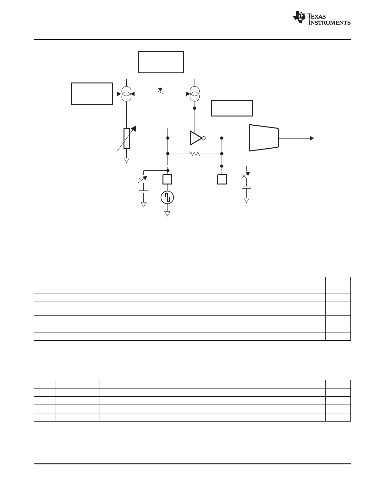
Signalswing
limitingcircuit
Biasgenerator
andstartup
circuit
XI
XO
Signal
shaping
Squarewave:
Vpp=VIO_1P8V
Y
Currentcontrol
circuitandmode
selection
Floating
VBATOK
(1)
Internal
GND
Internal
GND
VBATOK
(1)
037-040
TPS65930/TPS65920
SWCS037G–MAY 2008– REVISED APRIL 2011
www.ti.com
(1) Switches close by default and open only if register access enables very-low-power mode when VBAT < 2.7 V.
Figure 11-9. 32-kHz Oscillator in Bypass Mode Block Diagram Without Crystal Option 3
Table 11-7 lists the electrical constraints required by the 32-kHz input square- or sine-wave clock.
Table 11-7. 32-kHz Input Square- or Sine-Wave Clock Source Electrical Characteristics
Name Parameter Description Min Typ Max Unit
f Frequency 32.768 kHz
C
C
V
PP
V
IH
V
IL
(1) Bypass input maximum voltage is the same as the maximum voltage provided for the I/O interface.
Input capacitance 35 pF
I
On-chip foot capacitance to GND on each input (see Figure 11-7, Figure 11-8, and 10
FI
Figure 11-9)
Square-/sine-wave amplitude in bypass mode or not 1.8
(1)
Voltage input high, square wave in bypass mode 0.8 V
Voltage input low, square wave in bypass mode 0.6 V
Table 11-8 lists the timing requirements of the 32-kHz square-wave input clock.
Table 11-8. 32-kHz Square-Wave Input Clock Source Timing Requirements
Name Parameter Description Min Typ Max Unit
CK0 1/t
CK1 t
CK3 t
CK4 t
C(32KHZ)
W(32KHZ)
R(32KHZ)
F(32KHZ)
Frequency, 32 kHz 32.768 MHz
Pulse duration, 32 kHz low or high 0.45*t
Rise time, 32 kHz
Fall time, 32 kHz
(1) The capacitive load is 30 pF.
(1)
(1)
C(32KHZ)
0.55*t
C(32KHZ)
0.1*t
0.1*t
C(32KHZ)
C(32KHZ)
pF
V
μs
μs
μs
90 Clock Specifications Copyright © 2008–2011, Texas Instruments Incorporated
Submit Documentation Feedback
focus.ti.com: TPS65930/TPS65920

32KX
CK0 CK1CK1
037-038
OR
OR
32kHz
32KXIN
32KXOUT
32-kHz
OSC
IO_1P8
(1.8V)
32KCLKOUT
RTC
037-037
TPS65930/TPS65920
www.ti.com
Figure 11-10 shows the 32-kHz square- or sine-wave input clock.
Figure 11-10. 32-kHz Square- or Sine-Wave Input Clock
11.3 Output Clock Specifications
The TPS65920/TPS65930 device provides two output clocks:
• 32KCLKOUT
• HFCLKOUT
11.3.1 32KCLKOUT Output Clock
Figure 11-11 is the block diagram for the 32.768-kHz clock output.
SWCS037G–MAY 2008– REVISED APRIL 2011
Figure 11-11. 32.768-kHz Clock Output Block Diagram
The TPS65920/TPS65930 device has an internal 32.768-kHz oscillator connected to an external
32.768-kHz crystal through the 32KXIN/32KXOUT balls or an external digital 32.768-kHz clock through the
32KXIN input (see Figure 11-11). The TPS65920/TPS65930 device also generates a 32.768-kHz digital
clock through the 32KCLKOUT pin and can broadcast it externally to the application processor or any
other devices. The 32KCLKOUT clock is broadcast by default in TPS65920/TPS65930 active mode, but
can be disabled if it is not used.
The 32.768-kHz clock (or signal) is also used to clock the RTC embedded in the TPS65920/TPS65930
device. The RTC is not enabled by default. The host processor must set the correct date and time and
enable the RTC functionality.
The 32KCLKOUT output buffer can drive several devices (up to 40-pF load). At startup, 32KCLKOUT
must be stabilized (frequency/duty cycle) before the signal output. Depending on the startup conditions,
this can delay the startup sequence.
Table 11-9 lists the electrical characteristics of the 32KCLKOUT output clock.
Copyright © 2008–2011, Texas Instruments Incorporated Clock Specifications 91
Submit Documentation Feedback
focus.ti.com: TPS65930/TPS65920
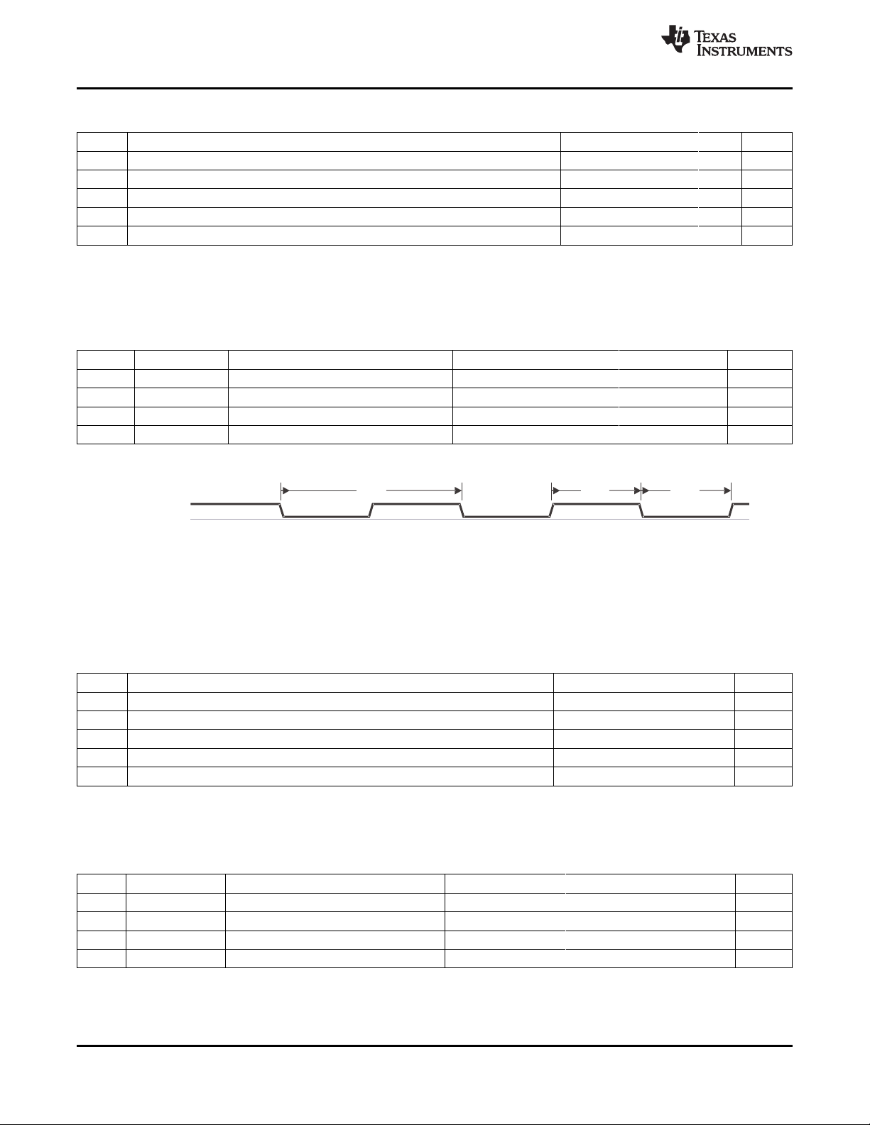
32KCLKOUT
CK0 CK1 CK1
037-035
TPS65930/TPS65920
SWCS037G–MAY 2008– REVISED APRIL 2011
www.ti.com
Table 11-9. 32KCLKOUT Output Clock Electrical Characteristics
Name Parameter Description Min Typ Max Unit
f Frequency 32.768 kHz
C
V
OUT
V
OH
V
OL
Load capacitance 40 pF
L
Output clock voltage, depending on output reference level IO_1P8 (see Section 2) 1.8
Voltage output high V
– 0.45 V
OUT
Voltage output low 0 0.45 V
(1)
OUT
(1) The output voltage depends on the output reference level, which is IO_1P8 (see Section 2, Terminal Description).
Table 11-10 lists the output clock switching characteristics. Figure 11-12 shows the 32KCLKOUT output
clock waveform.
Table 11-10. 32KCLKOUT Output Clock Switching Characteristics
Name Parameter Description Min Typ Max Unit
CK0 1/t
CK1 t
CK2 t
CK3 t
C(32KCLKOUT)
W(32KCLKOUT)
R(32KCLKOUT)
F(32KCLKOUT)
(1) The output capacitive load is 30 pF.
Frequency 32.768 MHz
Pulse duration, 32KCLKOUT low or high 0.40*t
Rise time, 32KCLKOUT
Fall time, 32KCLKOUT
(1)
(1)
C(32KCLKOUT)
0.60*t
C(32KCLKOUT)
16 ns
16 ns
ns
V
V
Figure 11-12. 32KCLKOUT Output Clock
11.3.2 HFCLKOUT Output Clock
Table 11-11 lists the electrical characteristics of the HFCLKOUT output clock.
Table 11-11. HFCLKOUT Output Clock Electrical Characteristics
Name Parameter Description Min Typ Max Unit
f Frequency 19.2, 26, or 38.4 MHz
C
V
OUT
V
OH
V
OL
(1) The output voltage depends on the output reference level, which is IO_1P8 (see Section 2).
Name Parameter Description Min Typ Max Unit
CHO1 1/t
CHO2 t
CHO3 t
CHO4 t
(1) The output capacitive load is 30 pF.
Load capacitance 30 pF
L
Output clock voltage, depending on output reference level IO_1P8 (see Section 2) 1.8
Voltage output high V
OUT
– 0.45 V
(1)
Voltage output low 0 0.45 V
Table 11-12 lists the switching characteristics of the HFCLKOUT output clock.
Table 11-12. HFCLKOUT Output Clock Switching Characteristics
C(HFCLKOUT)
W(HFCLKOUT)
R(HFCLKOUT)
F(HFCLKOUT)
Frequency 19.2, 26, or 38.4 MHz
Pulse duration, HFCLKOUT low or high 0.40*t
Rise time, HFCLKOUT
Fall time, HFCLKOUT
(1)
(1)
C(HFCLKOUT)
0.60*t
C(HFCLKOUT)
OUT
2.6 ns
2.6 ns
V
V
ns
92 Clock Specifications Copyright © 2008–2011, Texas Instruments Incorporated
Submit Documentation Feedback
focus.ti.com: TPS65930/TPS65920
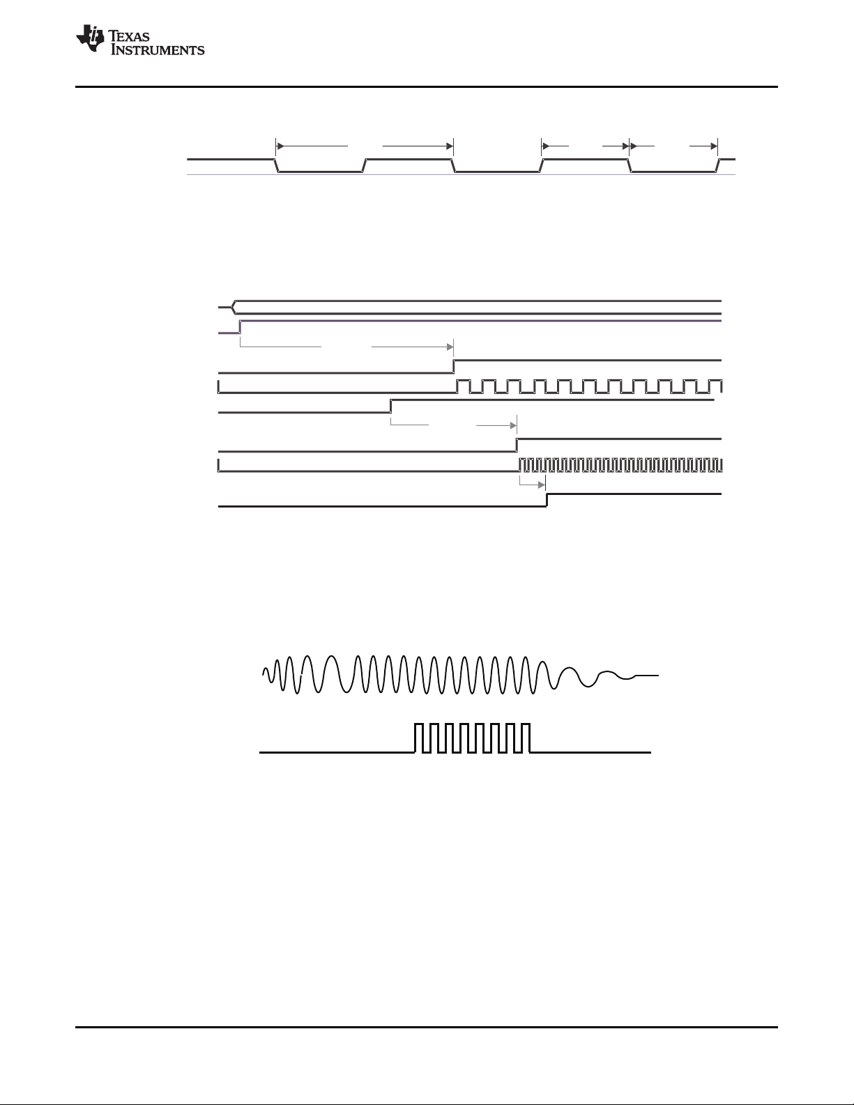
HFCLKOUT
CHO1 CHO2 CHO2
037-036
Tstartup
Delay1
Delay2
XIN
Starting_Event
CLK32KOUTEN
CLK32KOUT
CLKEN
HFCLKOUTEN
HFCLKOUT
NRESPWRON
037-034
HFCLKIN
HFCLKOUT
019-028
TPS65930/TPS65920
www.ti.com
Figure 11-13 shows the HFCLKOUT output clock waveform.
Figure 11-13. HFCLKOUT Output Clock
11.3.3 Output Clock Stabilization Time
Figure 11-14 shows the 32KCLKOUT and HFCLKOUT clock stabilization time.
SWCS037G–MAY 2008– REVISED APRIL 2011
NOTE: Tstartup, Delay1, and Delay2 depend on the boot mode (see Section 4.5, Power Management).
NOTE: Ensure that the high frequency oscillator start-up time is in spec for the boot mode used. During power-up the internal
delay, Delay1 above is fixed (5.2 ms and 5.3 ms depending on boot mode). The start-up time for the oscillator must
be less than the fixed delay.
Figure 11-14. 32KCLKOUT and HFCLKOUT Clock Stabilization Time
Figure 11-15 shows the HFCLKOUT behavior.
Figure 11-15. HFCLKOUT Behavior
Copyright © 2008–2011, Texas Instruments Incorporated Clock Specifications 93
Submit Documentation Feedback
focus.ti.com: TPS65930/TPS65920
TPS65930/TPS65920
SWCS037G–MAY 2008– REVISED APRIL 2011
12 Timing Requirements and Switching Characteristics
12.1 Timing Parameters
The timing parameter symbols used in the timing requirement and switching characteristic tables are
created in accordance with JEDEC Standard 100. To shorten the symbols, some pin names and other
related terminologies are abbreviated, as shown in Table 12-1.
Table 12-1. Timing Parameters
Subscripts
Symbol Parameter
c Cycle time (period)
d Delay time
dis Disable time
en Enable time
h Hold time
su Setup time
START Start bit
t Transition time
v Valid time
w Pulse duration (width)
X Unknown, changing, or don't care level
H High
L Low
V Valid
IV Invalid
AE Active edge
FE First edge
LE Last edge
Z High impedance
www.ti.com
94 Timing Requirements and Switching Characteristics Copyright © 2008–2011, Texas Instruments Incorporated
Submit Documentation Feedback
focus.ti.com: TPS65930/TPS65920
TPS65930/TPS65920
www.ti.com
SWCS037G–MAY 2008– REVISED APRIL 2011
12.2 Target Frequencies
Table 12-2 assumes testing over the recommended operating conditions.
Table 12-2. TPS65920/TPS65930 Interface Target Frequencies
I/O Interface Interface Designation
SmartReflex inter-integrated
circuit (I2C™)
General-purpose I2C Slave fast-speed mode 400 Kbps
USB FS 12 Mbps
JTAG XDS560 and XDS510 tools 30 MHz
TDM/inter-IC sound (I2S™)
Voice/Bluetooth® pulse code
modulation (PCM) interface
(1) Fs = 8 to 48 kHz; 96 kHz for RX path only (TDM/I2S interface)
(2) Fs = 8 or 16 kHz (voice/Bluetooth PCM interface)
I2C Slave HS mode 3.6 Mbps
Slave standard mode 100 Kbps
USB HS 480 Mbps
LS 1.5 Mbps
Real/View® ICE tool 30 MHz
Lauterbach™ tool 30 MHz
I2S 1/(64 * Fs)
Right-justified 1/(64 * Fs)
Left-justified 1/(64 * Fs)
TDM 1/(128 * Fs)
PCM (master mode) 1/(65 * Fs)
PCM (slave mode) 1/(33 to 65 * Fs)
Target Frequency
1.5 V
(1)
(1)
(1)
(1)
(2)
(2)
Copyright © 2008–2011, Texas Instruments Incorporated Timing Requirements and Switching Characteristics 95
Submit Documentation Feedback
focus.ti.com: TPS65930/TPS65920

I2C.SCL
I2C.SDA
1 8 9 1 8 9
MSB LSB
ACK
MSB LSB
ACK
I1 I2
I3 I4
I7
I8
I8
I9
START RESTART STOP
037-033
TPS65930/TPS65920
SWCS037G–MAY 2008– REVISED APRIL 2011
12.3 I2C Timing
The TPS65920/TPS65930 device provides two I2C HS slave interfaces (one for general-purpose and one
for SmartReflex). These interfaces support standard mode (100 Kbps), fast mode (400 Kbps), and HS
mode (3.4 Mbps). The general-purpose I2C module embeds four slave hard-coded addresses (ID1 = 48h,
ID2 = 49h, ID3 = 4Ah, and ID4 = 4Bh). The SmartReflex I2C module uses one slave hard-coded address
(ID5). The master mode is not supported.
Table 12-3 and Table 12-4 assume testing over the recommended operating conditions (see Figure 12-1).
Figure 12-1. I2C Interface—Transmit and Receive in Slave Mode
Table 12-3. I2C Interface—Timing Requirements
www.ti.com
(1) (2)
Notation Parameter Min Max Unit
Slave HS Mode
I3 t
I4 t
I7 t
I8 t
I9 t
su(SDA-SCLH)
h(SCLL-SDA)
su(SCLH-SDAL)
h(SDAL-SCLL)
su(SDAH-SCLH)
Setup time, SDA valid to SCL high 10 ns
Hold time, SDA valid from SCL low 0 70 ns
Setup time, SCL high to SDA low 160 ns
Hold time, SCL low from SDA low 160 ns
Setup time, SDA high to SCL high 160 ns
Slave Fast-Speed Mode
I3 t
I4 t
I7 t
I8 t
I9 t
su(SDA-SCLH)
h(SCLL-SDA)
su(SCLH-SDAL)
h(SDAL-SCLL)
su(SDAH-SCLH)
Setup time, SDA valid to SCL high 100 ns
Hold time, SDA valid from SCL low 0 0.9 ns
Setup time, SCL high to SDA low 0.6 ns
Hold time, SCL low from SDA low 0.6 ns
Setup time, SDA high to SCL high 0.6 ns
Slave Standard Mode
I3 t
I4 t
I7 t
I8 t
I9 t
su(SDA-SCLH)
h(SCLL-SDA)
su(SCLH-SDAL)
h(SDAL-SCLL)
su(SDAH-SCLH)
Setup time, SDA valid to SCL high 250 ns
Hold time, SDA valid from SCL low 0 ns
Setup time, SCL high to SDA low 4.7 ns
Hold time, SCL low from SDA low 4 ns
Setup time, SDA high to SCL high 4 ns
(1) The input timing requirements are given by considering a rising or falling time of:
80 ns in HS mode (3.4 Mbps)
300 ns in fast-speed mode (400 Kbps)
1000 ns in standard mode (100 Kbps)
(2) SDA is equal to I2C.SR.SDA or I2C.CNTL.SDA.
SCL is equal to I2C.SR.SCL or I2C.CNTL.SCL.
Table 12-4 lists the switching requirements of the I2C interface.
96 Timing Requirements and Switching Characteristics Copyright © 2008–2011, Texas Instruments Incorporated
Submit Documentation Feedback
focus.ti.com: TPS65930/TPS65920

TPS65930/TPS65920
www.ti.com
Table 12-4. I2C Interface—Switching Requirements
Notation Parameter Min Max Unit
Slave HS Mode
I1 t
I2 t
I1 t
I2 t
I1 t
I2 t
(1) The capacitive load is:
100 pF in HS mode (3.4 Mbps)
400 pF in fast-speed mode (400 Kbps)
400 pF in standard mode (100 Kbps)
(2) SDA is equal to I2C.SR.SDA or I2C.CNTL.SDA
SCL is equal to I2C.SR.SCL or I2C.CNTL.SCL
(3) SCL low timing for slave fast-speed mode is compatibile with 0.79 µs.
w(SCLL)
w(SCLH)
w(SCLL)
w(SCLH)
w(SCLL)
w(SCLH)
Pulse duration, SCL low 160 ns
Pulse duration, SCL high 60 ns
Slave Fast-Speed Mode
Pulse duration, SCL low 1.3
Pulse duration, SCL high 0.6 µs
Slave Standard Mode
Pulse duration, SCL low 4.7 µs
Pulse duration, SCL high 4 µs
12.4 Audio Interface: TDM/I2S Protocol
The TPS65920/TPS65930 device acts as a master for the TDM and I2S interfaces or as a slave for only
the I2S interface. If the TPS65920/TPS65930 device is the master, it must provide the frame
synchronization (TDM/I2S_SYNC) and bit clock (TDM/I2S_CLK) to the host processor. If it is the slave,
the TPS65920/TPS65930 device receives frame synchronization and the bit clock.
SWCS037G–MAY 2008– REVISED APRIL 2011
(1) (2)
(3)
µs
The TPS65920/TPS65930 device supports the I2S, TDM, left-justified, and right-justified data formats, but
does not support TDM slave mode.
Copyright © 2008–2011, Texas Instruments Incorporated Timing Requirements and Switching Characteristics 97
Submit Documentation Feedback
focus.ti.com: TPS65930/TPS65920

I2S.SYNC
I2S.CLK
I2S.DIN
I2S.DOUT
23
22 1
0
8dummybits
23
22 1
0
8dummybits
23
22
23
22 1
0
8dummybits
23
22
1
0
8dummybits
23
22
Leftchannel
Rightchannel
I2 I2 I2
I3 I3 I3
I3
I4 I4
I4
I4
I5
I5
I5 I5
I0 I1
I1
037-031
I2S.SYNC
I2S.CLK
I2S.DIN
I2S.DOUT
23
22 1
0
8dummybits
23
22
1
0
8dummybits
23
22
23
22 1
0
8dummybits
23
22 1
0
8dummybits
23
22
Leftchannel Rightchannel
I3 I3 I3 I3
I4 I4 I4 I4
I5 I5 I5 I5
I6 I7 I6I0 I1
I1
037-032
TPS65930/TPS65920
SWCS037G–MAY 2008– REVISED APRIL 2011
12.4.1 I2S Right- and Left-Justified Data Format
Table 12-5 and Table 12-6 assume testing over the recommended operating conditions (see Figure 12-2
and Figure 12-3).
Figure 12-2. I2S Interface—I2S Master ModeI
www.ti.com
Figure 12-3. I2S Interface—I2S Slave Mode
The timing requirements listed in Table 12-5 are valid on the following conditions of input slew and output
load:
• Rise and fall time range of inputs (SYNC, DIN) is tR/tF= 1.0 ns/6.5 ns
• Capacitance load range of outputs (CLK, SYNC, DOUT) is C
98 Timing Requirements and Switching Characteristics Copyright © 2008–2011, Texas Instruments Incorporated
Submit Documentation Feedback
focus.ti.com: TPS65930/TPS65920
= 1 pF/30 pF
Load

TPS65930/TPS65920
www.ti.com
The input timing requirements in Table 12-5 are given by considering a rising or falling time of 6.5 ns.
Table 12-5. I2S Interface—Timing Requirements
Notation Parameter Min Max Unit
I3 t
I4 t
I0 t
I1 t
I3 t
I4 t
I6 t
I7 t
su(DIN-CLKH)
h(DIN-CLKH)
c(CLK)
w(CLK)
su(DIN-CLKH)
h(DIN-CLKH)
su(SYNC-CLKH)
h(SYNC-CLKH)
(1) Fs = 8 to 48 kHz; 96 kHz for RX path only
(2) P = I2S.CLK period
The capacitive load for Table 12-6 is 7 pF. Table 12-6 lists the switching characteristics for the I2S
interface.
Table 12-6. I2S Interface—Switching Characteristics
SWCS037G–MAY 2008– REVISED APRIL 2011
Master Mode
Setup time, I2S.DIN valid to I2S.CLK high2 25 ns
Hold time, I2S.DIN valid from I2S.CLK high. 0 ns
Slave Mode
Cycle time, I2S.CLK
Pulse duration, I2S.CLK high or low
(1)
(2)
1/64 * Fs ns
0.45 * P 0.55 * P ns
Setup time, I2S.DIN valid to I2S.CLK high 5 ns
Hold time, I2S.DIN valid from I2S.CLK high. 5 ns
Setup time, I2S.SYNC valid to I2S.CLK high 5 ns
Hold time, I2S.SYNC valid from I2S.CLK high 5 ns
Notation Parameter Min Max Unit
I0 t
I1 t
I2 t
I5 t
I5 t
c(CLK)
w(CLK)
d(CLKL-SYNC)
d(CLKL-DOUT)
d(CLKL-DOUT)
(1) Fs = 8 to 48 kHz; 96 kHz for RX path only
(2) P = I2S.CLK period
Master Mode
Cycle time, I2S.CLK
Pulse duration, I2S.CLK high or low
(1)
(2)
1/64 * Fs ns
0.45 * P 0.55 * P ns
Delay time, I2S.CLK falling edge to I2S.SYNC –10 10 ns
transition
Delay time, I2S.CLK falling edge to I2S.DOUT –10 10 ns
transition
Slave Mode
Delay time, I2S.CLK falling edge to I2S.DOUT 0 20 ns
transition
Copyright © 2008–2011, Texas Instruments Incorporated Timing Requirements and Switching Characteristics 99
Submit Documentation Feedback
focus.ti.com: TPS65930/TPS65920

I2S.SYNC
I2S.CLK
I2S.DIN
I2S.DOUT
23
22 1
0 23
22
1
0 23
22 1
0 23
22 1
0
23
22
1
0
23
22 1
0 23
22 1
0 23
22 1
0
Channel1 Channel2 Channel3 Channel4
T1
T3 T3 T3 T3 T3 T3 T3 T3
T4 T4 T4 T4 T4 T4 T4 T4
T5 T5 T5 T5 T5 T5 T5 T5
T2 T2 T2 T2
T0 T1
8dummy
bits
8dummy
bits
8dummy
bits
8dummy
bits
8dummy
bits
8dummy
bits
037-030
TPS65930/TPS65920
SWCS037G–MAY 2008– REVISED APRIL 2011
12.4.2 TDM Data Format
Table 12-7 and Table 12-8 assume testing over the recommended operating conditions (see Figure 12-4).
Figure 12-4. TDM Interface—TDM Master Mode
www.ti.com
100 Timing Requirements and Switching Characteristics Copyright © 2008–2011, Texas Instruments Incorporated
Submit Documentation Feedback
focus.ti.com: TPS65930/TPS65920
 Loading...