

Page 1

TPS65917-Q1 Register Map
Technical Reference Manual
Literature Number: SLVUAH1C
June 2015–Revised April 2017
Page 2

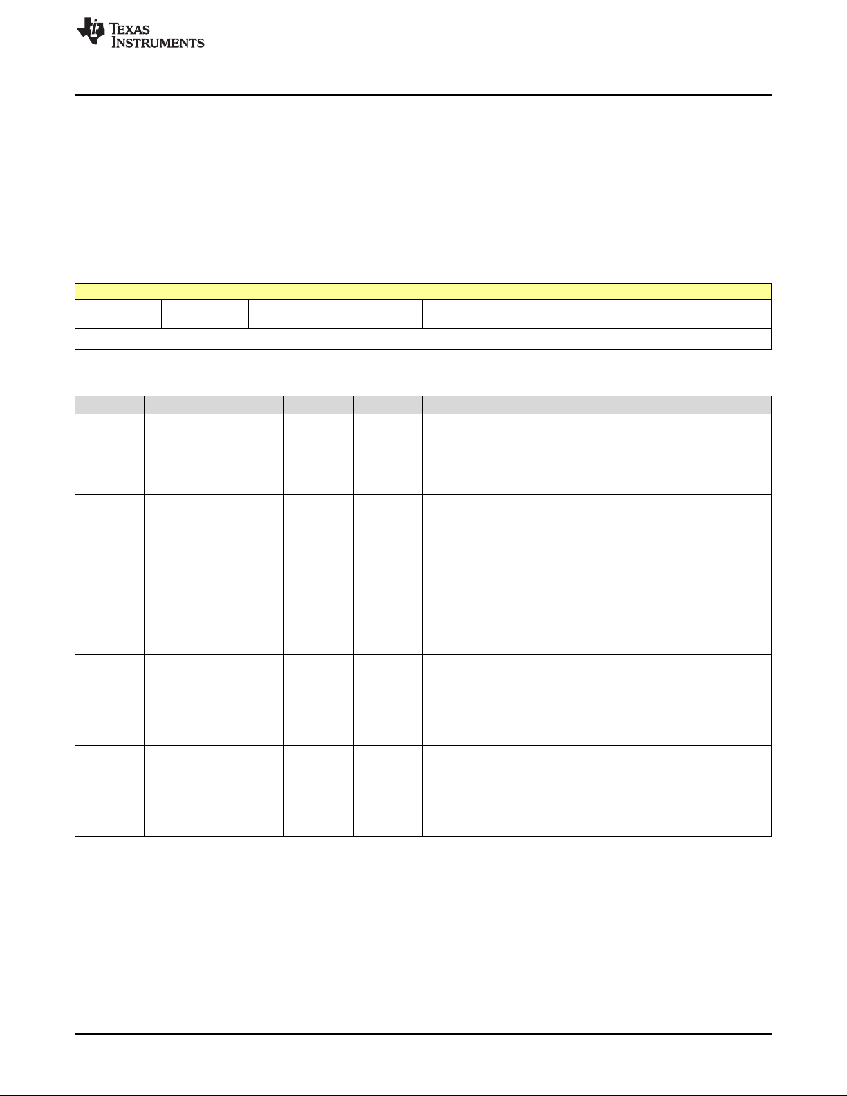
This document presents a summary of the hardware interface for the TPS65917-Q1 device. Each module
instance within the design is shown along with the module register map and bit definitions for each bitfield.
1.1 Register Address Mapping
This document describes the register mapping of the TPS65917-Q1 device. The operation of the IC is
described in the device data sheet, TPS65917-Q1 Power Management Unit (PMU) for Processor.
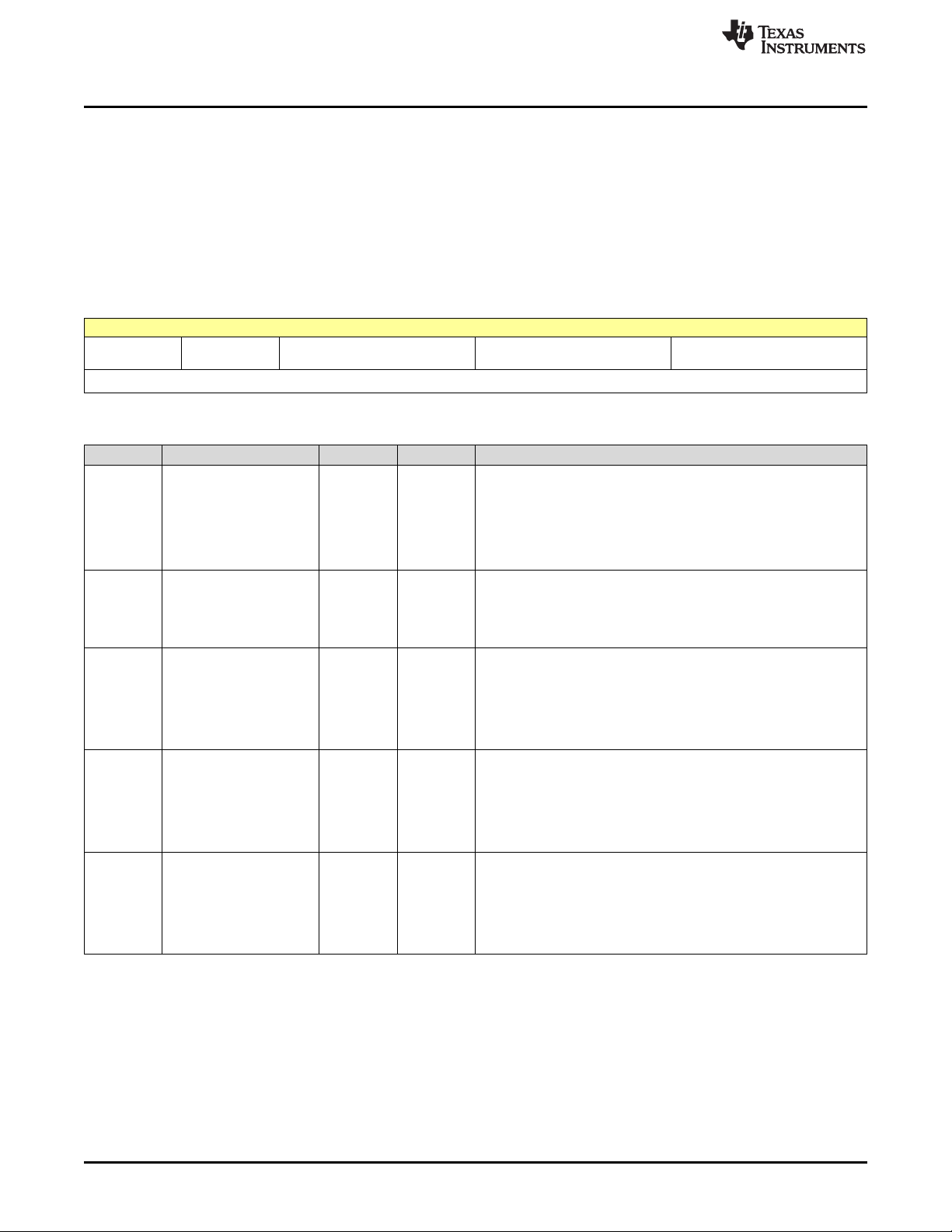
The 3 hex digits of the physical address of the register indicated in this document are mapped as 0xPAA,
while P stands for the page number of the register, and AA stands for the register address within the
memory page. The page numbers are mapped to the slave device address as following:
Page = 0x0 — Slave Device address 0x12 for DVS registers
Page = 0x1 — Slave Device address 0x48 or 0x58 for Power registers
Page = 0x2 — Slave Device address 0x49 or 0x59 for Interfaces and Auxiliaries registers
Page = 0x3 — Slave Device address 0x4A or 0x5A for Trimming and Test registers
Chapter 1
SLVUAH1C–June 2015–Revised April 2017
Introduction
Page = 0x4 —Slave Device address 0x4B or 0x5B for OTP programming registers
For the reset of the registers, the registers are defined by 3 categories:
• POR: Power On Reset registers
• HWRST: Hardware Reset registers
• SWORST: Switch Off Reset registers
These categories of registers (POR, HWRST, SWORST) are described in the device data sheet. When
the reset value of a bit register is 0bX, it means the bit value is coming from the OTP memory.
NOTE: All reserved bits are read only (R). Read to an unmapped register returns previous read
value.
2
Introduction
Copyright © 2015–2017, Texas Instruments Incorporated
SLVUAH1C–June 2015–Revised April 2017
Submit Documentation Feedback
Page 3
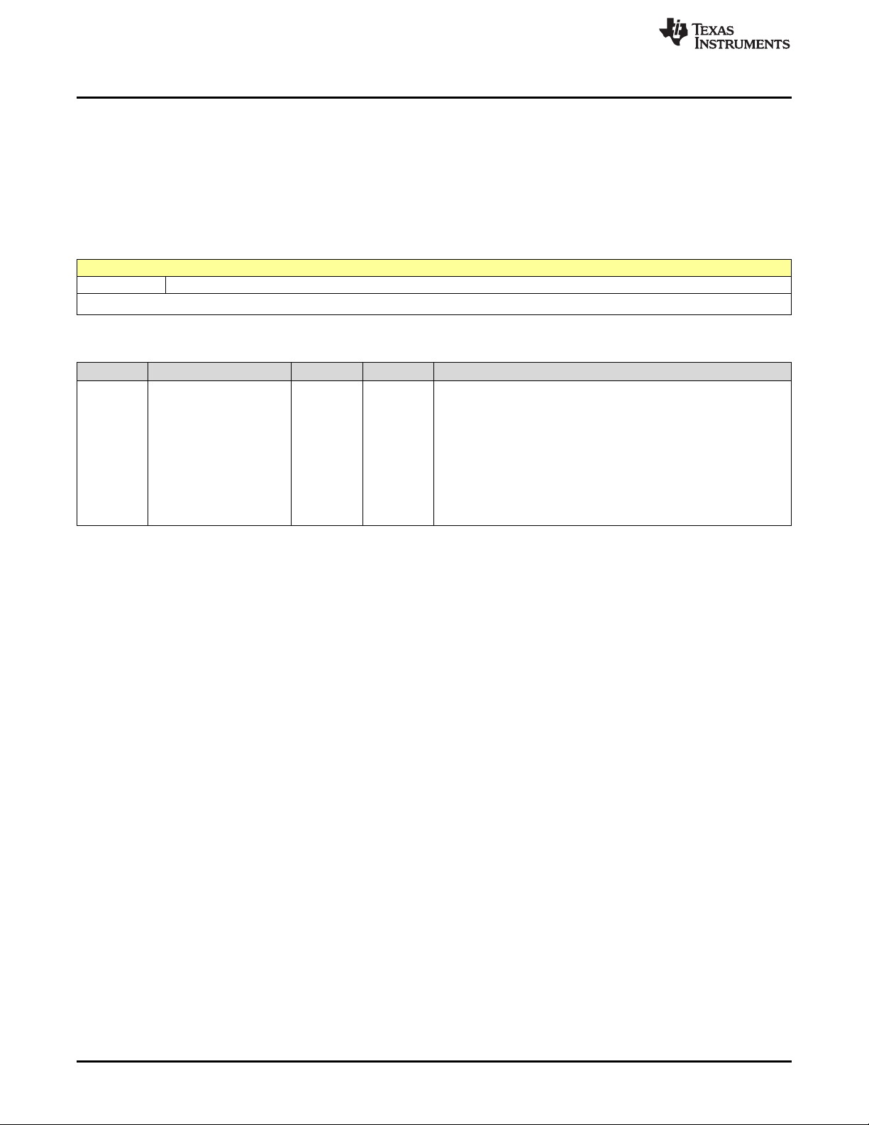
2.1 Register Module Base Address and Size
Table 2-1 lists the base address and address space for the TPS65917-Q1 device functional register
modules.
Table 2-1. TPS65917-Q1 Function Register Module Name and Base Address
Module Name Base Address Size
FUNC_SMPS_DVS 0x020 32 Bytes
FUNC_BACKUP 0x118 8 Bytes
FUNC_SMPS 0x120 48 Bytes
FUNC_LDO 0x150 47 Bytes
FUNC_SPI 0x17F 1 Byte
FUNC_DVFS 0x180 8 Bytes
FUNC_PMU_CONTROL 0x1A0 32 Bytes
FUNC_RESOURCE 0x1D4 28 Bytes
FUNC_PAD_CONTROL 0x1F0 16 Bytes
FUNC_INTERRUPT 0x210 32 Bytes
FUNC_ID 0x24F 4 Bytes
FUNC_GPIO 0x280 20 Bytes
FUNC_GPADC 0x2C0 32 Bytes
FUNC_DESIGNREV 0x357 1 Byte
FUNC_TRIM_GPADC 0x3CD 18 Bytes
Chapter 2
SLVUAH1C–June 2015–Revised April 2017
Register Physical Address
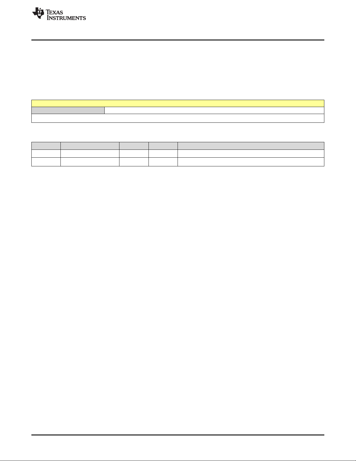
Complex bit access types are encoded to fit into small table cells. Table 2-2 shows the codes that are
used for access types in this document.
Table 2-2. FUNC_PAD_CONTROL Access Type Codes
Access Type Code Description
Read Type
R R Read
RC R
Write Type
W W Write
SLVUAH1C–June 2015–Revised April 2017
Submit Documentation Feedback
C
Copyright © 2015–2017, Texas Instruments Incorporated
Read
to Clear
Register Physical Address
3
Page 4

Chapter 3
SLVUAH1C–June 2015–Revised April 2017
Register Descriptions
3.1 FUNC_SMPS_DVS Registers
Table 3-1 lists the memory-mapped registers for the FUNC_SMPS_DVS. All register offset addresses not
listed in Table 3-1 should be considered as reserved locations and the register contents should not be
modified.
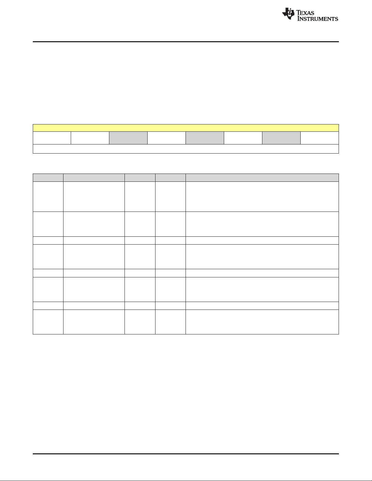
Table 3-1. FUNC_SMPS_DVS Registers
Address Acronym Register Name Section
22h SMPS1_FORCE SMPS1 (or SMPS12 in case of dual-phase) DVS
register.
Voltage to apply to the resource when it is a DVS force
command (OTP_Config).
RESET register domain: SWORST
23h SMPS1_VOLTAGE SMPS1 (or SMPS12 in case of dual-phase) DVS
register.
Voltage to apply to the resource when it is not a DVS
force command (OTP_Config).r.
RESET register domain: SWORST
26h SMPS2_FORCE SMPS2 DVS register.
Voltage to apply to the resource when it is a DVS force
command (OTP_Config).
RESET register domain: SWORST
27h SMPS2_VOLTAGE SMPS2 DVS register.
Voltage to apply to the resource when it is not a DVS
force command (OTP_Config).
RESET register domain: SWORST
2Eh SMPS3_FORCE SMPS3 DVS register.
Voltage to apply to the resource when it is a DVS force
command (OTP_Config).
RESET register domain: SWORST
2Fh SMPS3_VOLTAGE SMPS3 DVS register.
Voltage to apply to the resource when it is not a DVS
force command (OTP_Config).
RESET register domain: SWORST
Section 3.1.1
Section 3.1.2
Section 3.1.3
Section 3.1.4
Section 3.1.5
Section 3.1.6
4
Register Descriptions
Copyright © 2015–2017, Texas Instruments Incorporated
SLVUAH1C–June 2015–Revised April 2017
Submit Documentation Feedback
Page 5

www.ti.com
FUNC_SMPS_DVS Registers
3.1.1 SMPS1_FORCE Register (Address = 22h) [reset = X]
SMPS1_FORCE is shown in Figure 3-1 and described in Table 3-2.
Return to Summary Table.
SMPS1 (or SMPS12 in case of dual-phase) DVS register. Voltage to apply to the resource when it is a
DVS force command (OTP_Config).
RESET register domain: SWORST
Figure 3-1. SMPS1_FORCE Register
7 6 5 4 3 2 1 0
CMD VSEL
R/W-1h R/W-X
Table 3-2. SMPS1_FORCE Register Field Descriptions
Bit Field Type Reset Description
7 CMD R/W 1h
6-0 VSEL R/W X
DVS command register selection:
When 0: SMPS1_FORCE.VSEL voltage is applied
When 1: SMPS1_VOLTAGE.VSEL voltage is applied (default)
CMD is effective if SMPS1_CTRL.ROOF_FLOOR_EN='0'
See VSEL cross table showed in SMPS1_VOLTAGE.VSEL register
(page1).
SLVUAH1C–June 2015–Revised April 2017
Submit Documentation Feedback
Copyright © 2015–2017, Texas Instruments Incorporated
Register Descriptions
5
Page 6
FUNC_SMPS_DVS Registers
3.1.2 SMPS1_VOLTAGE Register (Address = 23h) [reset = X]
SMPS1_VOLTAGE is shown in Figure 3-2 and described in Table 3-3.
Return to Summary Table.
SMPS1 (or SMPS12 in case of dual-phase) DVS register. Voltage to apply to the resource when it is not a
DVS force command (OTP_Config).r.
RESET register domain: SWORST
Figure 3-2. SMPS1_VOLTAGE Register
7 6 5 4 3 2 1 0
RANGE VSEL
R/W-X R/W-X
Table 3-3. SMPS1_VOLTAGE Register Field Descriptions
Bit Field Type Reset Description
7 RANGE R/W X
6-0 VSEL R/W X
Range of the VSEL voltage. This bit is applied to
SMPS1_VOLTAGE.VSEL and SPMS1_FORCE.VSEL
0: 0.5V to 1.65V
1: 1.0 to 3.3V
Note:RANGE bit is RO when SMPS1 is ON, RANGE bit is RW when
SMPS1 is OFF
Note: For Dual-phase mode, RANGE=1 (1V to 3.3V) is not
supported.
See VSEL cross table showed in SMPS1_VOLTAGE.VSEL register
(page1).
www.ti.com
6
Register Descriptions
Copyright © 2015–2017, Texas Instruments Incorporated
SLVUAH1C–June 2015–Revised April 2017
Submit Documentation Feedback
Page 7
www.ti.com
FUNC_SMPS_DVS Registers
3.1.3 SMPS2_FORCE Register (Address = 26h) [reset = X]
SMPS2_FORCE is shown in Figure 3-3 and described in Table 3-4.
Return to Summary Table.
SMPS2 DVS register. Voltage to apply to the resource when it is a DVS force command (OTP_Config).
RESET register domain: SWORST
Figure 3-3. SMPS2_FORCE Register
7 6 5 4 3 2 1 0
CMD VSEL
R/W-1h R/W-X
Table 3-4. SMPS2_FORCE Register Field Descriptions
Bit Field Type Reset Description
7 CMD R/W 1h
6-0 VSEL R/W X
DVS command register selection:
When 0: SMPS2_FORCE.VSEL voltage is applied
When 1: SMPS2_VOLTAGE.VSEL voltage is applied (default)
CMD is effective if SMPS2_CTRL.ROOF_FLOOR_EN='0'
See VSEL cross table showed in SMPS1_VOLTAGE.VSEL register.
SLVUAH1C–June 2015–Revised April 2017
Submit Documentation Feedback
Copyright © 2015–2017, Texas Instruments Incorporated
Register Descriptions
7
Page 8

FUNC_SMPS_DVS Registers
3.1.4 SMPS2_VOLTAGE Register (Address = 27h) [reset = X]
SMPS2_VOLTAGE is shown in Figure 3-4 and described in Table 3-5.
Return to Summary Table.
SMPS2 DVS register. Voltage to apply to the resource when it is not a DVS force command
(OTP_Config).
RESET register domain: SWORST
Figure 3-4. SMPS2_VOLTAGE Register
7 6 5 4 3 2 1 0
RANGE VSEL
R/W-X R/W-X
Table 3-5. SMPS2_VOLTAGE Register Field Descriptions
Bit Field Type Reset Description
7 RANGE R/W X
6-0 VSEL R/W X
Range of the VSEL voltage. This bit is applied to
SMPS2_VOLTAGE.VSEL
0: 0.5V to 1.65V
1: 1.0 to 3.3V
Note:RANGE bit is RO when SMPS2 is ON, RANGE bit is RW when
SMPS2 is OFF
See VSEL cross table showed in SMPS1_VOLTAGE.VSEL register.
www.ti.com
8
Register Descriptions
Copyright © 2015–2017, Texas Instruments Incorporated
SLVUAH1C–June 2015–Revised April 2017
Submit Documentation Feedback
Page 9

www.ti.com
FUNC_SMPS_DVS Registers
3.1.5 SMPS3_FORCE Register (Address = 2Eh) [reset = X]
SMPS3_FORCE is shown in Figure 3-5 and described in Table 3-6.
Return to Summary Table.
SMPS3 DVS register. Voltage to apply to the resource when it is a DVS force command (OTP_Config).
RESET register domain: SWORST
Figure 3-5. SMPS3_FORCE Register
7 6 5 4 3 2 1 0
CMD VSEL
R/W-1h R/W-X
Table 3-6. SMPS3_FORCE Register Field Descriptions
Bit Field Type Reset Description
7 CMD R/W 1h
6-0 VSEL R/W X
DVS command register selection:
When 0: SMPS3_FORCE.VSEL voltage is applied
When 1: SMPS3_VOLTAGE.VSEL voltage is applied (default)
CMD is effective if SMPS3_CTRL.ROOF_FLOOR_EN='0'
See VSEL cross table showed in SMPS1_VOLTAGE.VSEL register
(page1).
SLVUAH1C–June 2015–Revised April 2017
Submit Documentation Feedback
Copyright © 2015–2017, Texas Instruments Incorporated
Register Descriptions
9
Page 10

FUNC_SMPS_DVS Registers
3.1.6 SMPS3_VOLTAGE Register (Address = 2Fh) [reset = X]
SMPS3_VOLTAGE is shown in Figure 3-6 and described in Table 3-7.
Return to Summary Table.
SMPS3 DVS register. Voltage to apply to the resource when it is not a DVS force command
(OTP_Config).
RESET register domain: SWORST
Figure 3-6. SMPS3_VOLTAGE Register
7 6 5 4 3 2 1 0
RANGE VSEL
R/W-X R/W-X
Table 3-7. SMPS3_VOLTAGE Register Field Descriptions
Bit Field Type Reset Description
7 RANGE R/W X
6-0 VSEL R/W X
Range of the VSEL voltage. This bit is applied to
SMPS3_VOLTAGE.VSEL and SPMS3_FORCE.VSEL
0: 0.5V to 1.65V
1: 1.0 to 3.3V
Note:RANGE bit is RO when SMPS3 is ON, RANGE bit is RW when
SMPS3 is OFF
See VSEL cross table showed in SMPS1_VOLTAGE.VSEL register
(page1).
www.ti.com
10
Register Descriptions
Copyright © 2015–2017, Texas Instruments Incorporated
SLVUAH1C–June 2015–Revised April 2017
Submit Documentation Feedback
Page 11

www.ti.com
FUNC_BACKUP Registers
3.2 FUNC_BACKUP Registers
Table 3-8 lists the memory-mapped registers for the FUNC_BACKUP. All register offset addresses not
listed in Table 3-8 should be considered as reserved locations and the register contents should not be
modified.
Table 3-8. FUNC_BACKUP Registers
Address Acronym Register Name Section
118h BACKUP0 Backup register #0 which can be used for storage by the
application firmware when the external host is power
down.
These registers will retain their content as long as VRTC
is active.
RESET register domain: POR
119h BACKUP1 Backup register #1 which can be used for storage by the
application firmware when the external host is power
down.
These registers will retain their content as long as VRTC
is active.
RESET register domain: POR
11Ah BACKUP2 Backup register #2 which can be used for storage by the
application firmware when the external host is power
down.
These registers will retain their content as long as VRTC
is active.
RESET register domain: POR
11Bh BACKUP3 Backup register #3 which can be used for storage by the
application firmware when the external host is power
down.
These registers will retain their content as long as VRTC
is active.
RESET register domain: POR
11Ch BACKUP4 Backup register #4 which can be used for storage by the
application firmware when the external host is power
down.
These registers will retain their content as long as VRTC
is active.
RESET register domain: POR
11Dh BACKUP5 Backup register #5 which can be used for storage by the
application firmware when the external host is power
down.
These registers will retain their content as long as VRTC
is active.
RESET register domain: POR
11Eh BACKUP6 Backup register #6 which can be used for storage by the
application firmware when the external host is power
down.
These registers will retain their content as long as VRTC
is active.
RESET register domain: POR
11Fh BACKUP7 Backup register #7 which can be used for storage by the
application firmware when the external host is power
down.
These registers will retain their content as long as VRTC
is active.
RESET register domain: POR
Section 3.2.1
Section 3.2.2
Section 3.2.3
Section 3.2.4
Section 3.2.5
Section 3.2.6
Section 3.2.7
Section 3.2.8
SLVUAH1C–June 2015–Revised April 2017
Submit Documentation Feedback
Copyright © 2015–2017, Texas Instruments Incorporated
Register Descriptions
11
Page 12

FUNC_BACKUP Registers
3.2.1 BACKUP0 Register (Address = 118h) [reset = 0h]
BACKUP0 is shown in Figure 3-7 and described in Table 3-9.
Return to Summary Table.
Backup register #0 which can be used for storage by the application firmware when the external host is
power down. These registers will retain their content as long as VRTC is active.
RESET register domain: POR
Figure 3-7. BACKUP0 Register
7 6 5 4 3 2 1 0
BACKUP
R/W-0h
Table 3-9. BACKUP0 Register Field Descriptions
Bit Field Type Reset Description
7-0 BACKUP R/W 0h
www.ti.com
12
Register Descriptions
Copyright © 2015–2017, Texas Instruments Incorporated
SLVUAH1C–June 2015–Revised April 2017
Submit Documentation Feedback
Page 13

www.ti.com
FUNC_BACKUP Registers
3.2.2 BACKUP1 Register (Address = 119h) [reset = 0h]
BACKUP1 is shown in Figure 3-8 and described in Table 3-10.
Return to Summary Table.
Backup register #1 which can be used for storage by the application firmware when the external host is
power down. These registers will retain their content as long as VRTC is active.
RESET register domain: POR
Figure 3-8. BACKUP1 Register
7 6 5 4 3 2 1 0
BACKUP
R/W-0h
Table 3-10. BACKUP1 Register Field Descriptions
Bit Field Type Reset Description
7-0 BACKUP R/W 0h
SLVUAH1C–June 2015–Revised April 2017
Submit Documentation Feedback
Copyright © 2015–2017, Texas Instruments Incorporated
Register Descriptions
13
Page 14

FUNC_BACKUP Registers
3.2.3 BACKUP2 Register (Address = 11Ah) [reset = 0h]
BACKUP2 is shown in Figure 3-9 and described in Table 3-11.
Return to Summary Table.
Backup register #2 which can be used for storage by the application firmware when the external host is
power down. These registers will retain their content as long as VRTC is active.
RESET register domain: POR
Figure 3-9. BACKUP2 Register
7 6 5 4 3 2 1 0
BACKUP
R/W-0h
Table 3-11. BACKUP2 Register Field Descriptions
Bit Field Type Reset Description
7-0 BACKUP R/W 0h
www.ti.com
14
Register Descriptions
Copyright © 2015–2017, Texas Instruments Incorporated
SLVUAH1C–June 2015–Revised April 2017
Submit Documentation Feedback
Page 15

www.ti.com
FUNC_BACKUP Registers
3.2.4 BACKUP3 Register (Address = 11Bh) [reset = 0h]
BACKUP3 is shown in Figure 3-10 and described in Table 3-12.
Return to Summary Table.
Backup register #3 which can be used for storage by the application firmware when the external host is
power down. These registers will retain their content as long as VRTC is active.
RESET register domain: POR
Figure 3-10. BACKUP3 Register
7 6 5 4 3 2 1 0
BACKUP
R/W-0h
Table 3-12. BACKUP3 Register Field Descriptions
Bit Field Type Reset Description
7-0 BACKUP R/W 0h
SLVUAH1C–June 2015–Revised April 2017
Submit Documentation Feedback
Copyright © 2015–2017, Texas Instruments Incorporated
Register Descriptions
15
Page 16
FUNC_BACKUP Registers
3.2.5 BACKUP4 Register (Address = 11Ch) [reset = 0h]
BACKUP4 is shown in Figure 3-11 and described in Table 3-13.
Return to Summary Table.
Backup register #4 which can be used for storage by the application firmware when the external host is
power down. These registers will retain their content as long as VRTC is active.
RESET register domain: POR
Figure 3-11. BACKUP4 Register
7 6 5 4 3 2 1 0
BACKUP
R/W-0h
Table 3-13. BACKUP4 Register Field Descriptions
Bit Field Type Reset Description
7-0 BACKUP R/W 0h
www.ti.com
16
Register Descriptions
Copyright © 2015–2017, Texas Instruments Incorporated
SLVUAH1C–June 2015–Revised April 2017
Submit Documentation Feedback
Page 17

www.ti.com
FUNC_BACKUP Registers
3.2.6 BACKUP5 Register (Address = 11Dh) [reset = 0h]
BACKUP5 is shown in Figure 3-12 and described in Table 3-14.
Return to Summary Table.
Backup register #5 which can be used for storage by the application firmware when the external host is
power down. These registers will retain their content as long as VRTC is active.
RESET register domain: POR
Figure 3-12. BACKUP5 Register
7 6 5 4 3 2 1 0
BACKUP
R/W-0h
Table 3-14. BACKUP5 Register Field Descriptions
Bit Field Type Reset Description
7-0 BACKUP R/W 0h
SLVUAH1C–June 2015–Revised April 2017
Submit Documentation Feedback
Copyright © 2015–2017, Texas Instruments Incorporated
Register Descriptions
17
Page 18

FUNC_BACKUP Registers
3.2.7 BACKUP6 Register (Address = 11Eh) [reset = 0h]
BACKUP6 is shown in Figure 3-13 and described in Table 3-15.
Return to Summary Table.
Backup register #6 which can be used for storage by the application firmware when the external host is
power down. These registers will retain their content as long as VRTC is active.
RESET register domain: POR
Figure 3-13. BACKUP6 Register
7 6 5 4 3 2 1 0
BACKUP
R/W-0h
Table 3-15. BACKUP6 Register Field Descriptions
Bit Field Type Reset Description
7-0 BACKUP R/W 0h
www.ti.com
18
Register Descriptions
Copyright © 2015–2017, Texas Instruments Incorporated
SLVUAH1C–June 2015–Revised April 2017
Submit Documentation Feedback
Page 19
www.ti.com
FUNC_BACKUP Registers
3.2.8 BACKUP7 Register (Address = 11Fh) [reset = 0h]
BACKUP7 is shown in Figure 3-14 and described in Table 3-16.
Return to Summary Table.
Backup register #7 which can be used for storage by the application firmware when the external host is
power down. These registers will retain their content as long as VRTC is active.
RESET register domain: POR
Figure 3-14. BACKUP7 Register
7 6 5 4 3 2 1 0
BACKUP
R/W-0h
Table 3-16. BACKUP7 Register Field Descriptions
Bit Field Type Reset Description
7-0 BACKUP R/W 0h
SLVUAH1C–June 2015–Revised April 2017
Submit Documentation Feedback
Copyright © 2015–2017, Texas Instruments Incorporated
Register Descriptions
19
Page 20

FUNC_SMPS Registers
3.3 FUNC_SMPS Registers
Table 3-17 lists the memory-mapped registers for the FUNC_SMPS. All register offset addresses not
listed in Table 3-17 should be considered as reserved locations and the register contents should not be
modified.
Table 3-17. FUNC_SMPS Registers
Address Acronym Register Name Section
120h SMPS1_CTRL SMPS1 (or SMPS12 in case of dual-phase) control
register.
RESET register domain: HWRST (MODE_ACTIVE and
MODE_SLEEP are in SWORST domain)
Notes: MODE_SLEEP is used when NSLEEP,
ENABLE1, ENABLE2 signals select the resource.
MODE_ACTIVE is used when none of NSLEEP,
ENABLE1, ENABLE2 signals select resource (see
Resources SLEEP/ACTIVE assignments table in the
Data Manual for details).
122h SMPS1_FORCE SMPS1 (or SMPS12 in case of dual-phase) DVS
register.
Voltage to apply to the resource when it is a DVS force
command (OTP_Config).
RESET register domain: SWORST
123h SMPS1_VOLTAGE SMPS1 (or SMPS12 in case of dual-phase) DVS
register.
Voltage to apply to the resource when it is not a DVS
force command (OTP_Config).
RESET register domain: SWORST
124h SMPS2_CTRL SMPS2 control register.
RESET register domain: HWRST (MODE_ACTIVE and
MODE_SLEEP are in SWORST domain)
Notes: MODE_SLEEP is used when NSLEEP,
ENABLE1, ENABLE2 signals select the resource.
MODE_ACTIVE is used when none of NSLEEP,
ENABLE1, ENABLE2 signals select resource (see
Resources SLEEP/ACTIVE assignments table in the
Data Manual for details).
126h SMPS2_FORCE SMPS2 DVS register.
Voltage to apply to the resource when it is a DVS force
command (OTP_Config).
RESET register domain: SWORST
127h SMPS2_VOLTAGE SMPS2 DVS register.
Voltage to apply to the resource when it is not a DVS
force command (OTP_Config).
RESET register domain: SWORST
12Ch SMPS3_CTRL SMPS3 control register.
RESET register domain: HWRST (MODE_ACTIVE and
MODE_SLEEP are in SWORST domain)
Notes: MODE_SLEEP is used when NSLEEP,
ENABLE1, ENABLE2 signals select the resource.
MODE_ACTIVE is used when none of NSLEEP,
ENABLE1, ENABLE2 signals select resource (see
Resources SLEEP/ACTIVE assignments table in the
Data Manual for details).
12Eh SMPS3_FORCE SMPS3
DVS register.
Voltage to apply to the resource when it is a DVS force
command (OTP_Config).
RESET register domain: SWORST
12Fh SMPS3_VOLTAGE SMPS3 DVS register.
Voltage to apply to the resource when it is not a DVS
force command (OTP_Config).
RESET register domain: SWORST
Section 3.3.1
Section 3.3.2
Section 3.3.3
Section 3.3.4
Section 3.3.5
Section 3.3.6
Section 3.3.7
Section 3.3.8
Section 3.3.9
www.ti.com
20
Register Descriptions
Copyright © 2015–2017, Texas Instruments Incorporated
SLVUAH1C–June 2015–Revised April 2017
Submit Documentation Feedback
Page 21
www.ti.com
FUNC_SMPS Registers
Table 3-17. FUNC_SMPS Registers (continued)
Address Acronym Register Name Section
130h SMPS4_CTRL SMPS4 control register.
RESET register domain: HWRST (MODE_ACTIVE and
MODE_SLEEP are in SWORST domain)
Notes: MODE_SLEEP is used when NSLEEP,
ENABLE1, ENABLE2 signals select the resource.
MODE_ACTIVE is used when none of NSLEEP,
ENABLE1, ENABLE2 signals select resource (see
Resources SLEEP/ACTIVE assignments table in the
Data Manual for details).
133h SMPS4_VOLTAGE SMPS4 register.
Voltage to apply to the resource.
RESET register domain: SWORST
138h SMPS5_CTRL SMPS5 control register.
RESET register domain: HWRST (MODE_ACTIVE and
MODE_SLEEP are in SWORST domain)
Notes: MODE_SLEEP is used when NSLEEP,
ENABLE1, ENABLE2 signals select the resource.
MODE_ACTIVE is used when none of NSLEEP,
ENABLE1, ENABLE2 signals select resource (see
Resources SLEEP/ACTIVE assignments table in the
Data Manual for details).
13Bh SMPS5_VOLTAGE MPS5 register.
Voltage to apply to the resource.
RESET register domain: SWORST
144h SMPS_CTRL SMPS control register.
RESET register domain: HWRST
145h SMPS_PD_CTRL SMPS Pull-Down enable register.
RESET register domain: HWRST
Notes:
SMPS pull-down register bits validate the control of the
active discharge of each power resource to full-fill the
turn-off timing requirements.
When a pull-down is not enabled, there is always a weak
pull-down present at the output of the power resource,
so that the device restart correctly at the next power-up
sequence.
147h SMPS_THERMAL_EN SMPS Thermal feature enable register.
RESET register domain: HWRST
148h SMPS_THERMAL_STATUS SMPS Thermal status register.
RESET register domain: POR
149h SMPS_SHORT_STATUS SMPS Short circuit status.
RESET register domain: POR
14Ah SMPS_NEGATIVE_CURRENT_LIMIT_EN Iload Negative Current Comparator enable register
(Negative Current measurement).
RESET register domain: HWRST
14Bh SMPS_POWERGOOD_MASK1 SMPS Power Good (POWERGOOD) mask #1
RESET register domain: POR
14Ch SMPS_POWERGOOD_MASK2 SMPS Power Good (POWERGOOD) mask #2
RESET register domain: POR (excepted
POWERGOOD_TYPE_SELECT which is under
HWRST)
14Dh SMPS_PLL_CTRL SMPS PLL control register.
RESET register domain: HWRST
Section 3.3.10
Section 3.3.11
Section 3.3.12
Section 3.3.13
Section 3.3.14
Section 3.3.15
Section 3.3.16
Section 3.3.17
Section 3.3.18
Section 3.3.19
Section 3.3.20
Section 3.3.21
Section 3.3.22
SLVUAH1C–June 2015–Revised April 2017
Submit Documentation Feedback
Copyright © 2015–2017, Texas Instruments Incorporated
Register Descriptions
21
Page 22
FUNC_SMPS Registers
3.3.1 SMPS1_CTRL Register (Address = 120h) [reset = 0h]
SMPS1_CTRL is shown in Figure 3-15 and described in Table 3-18.
Return to Summary Table.
SMPS1 (or SMPS12 in case of dual-phase) control register.
RESET register domain: HWRST (MODE_ACTIVE and MODE_SLEEP are in SWORST domain)
Notes: MODE_SLEEP is used when NSLEEP, ENABLE1, ENABLE2 signals select the resource.
MODE_ACTIVE is used when none of NSLEEP, ENABLE1, ENABLE2 signals select resource (see
Resources SLEEP/ACTIVE assignments table in the Data Manual for details).
Figure 3-15. SMPS1_CTRL Register
7 6 5 4 3 2 1 0
WR_S ROOF_FLOOR
_EN
R/W-0h R/W-0h R-0h R/W-0h R/W-0h
Table 3-18. SMPS1_CTRL Register Field Descriptions
Bit Field Type Reset Description
7 WR_S R/W 0h
6 ROOF_FLOOR_EN R/W 0h
5-4 STATUS R 0h
3-2 MODE_SLEEP R/W 0h
1-0 MODE_ACTIVE R/W 0h
STATUS MODE_SLEEP MODE_ACTIVE
Warm reset sensitivity
0: Re-load the default value (from OTP) in SMPS1_VOLTAGE.VSEL
and SMPS1_FORCE.VSEL register and re-load the default value
(reset value) in SMPS1_FORCE.CMD during Warm Reset.
1: Maintain current voltage during Warm Reset (Registers remain
unchanged - no voltage change).
Roof Floor enable bit (only for DVS)
0: Voltage Selection controlled by SMPS1_FORCE.CMD bit.
1: Voltage Selection controlled by device resource pins (NSLEEP,
ENABLE1, ENABLE2).
SMPS1 (or SMPS12 in case of dual-phase) status
00: OFF
01: Forced PWM
10: ECO
11: Forced PWM
SMPS1 (or SMPS12 in case of dual-phase) SLEEP Mode
00: OFF (default)
01: Forced PWM
10: ECO
11: Forced PWM
SMPS1 (or SMPS12 in case of dual-phase) ACTIVE Mode
00: OFF (default)
01: Forced PWM
10: ECO
11: Forced PWM
www.ti.com
22
Register Descriptions
Copyright © 2015–2017, Texas Instruments Incorporated
SLVUAH1C–June 2015–Revised April 2017
Submit Documentation Feedback
Page 23

www.ti.com
FUNC_SMPS Registers
3.3.2 SMPS1_FORCE Register (Address = 122h) [reset = X]
SMPS1_FORCE is shown in Figure 3-16 and described in Table 3-19.
Return to Summary Table.
SMPS1 (or SMPS12 in case of dual-phase) DVS register. Voltage to apply to the resource when it is a
DVS force command (OTP_Config).
RESET register domain: SWORST
Figure 3-16. SMPS1_FORCE Register
7 6 5 4 3 2 1 0
CMD VSEL
R/W-1h R/W-X
Table 3-19. SMPS1_FORCE Register Field Descriptions
Bit Field Type Reset Description
7 CMD R/W 1h
6-0 VSEL R/W X
DVS command register selection:
When 0: SMPS1_FORCE.VSEL voltage is applied
When 1: SMPS1_VOLTAGE.VSEL voltage is applied (default)
CMD is effective if SMPS1_CTRL.ROOF_FLOOR_EN='0'
See VSEL cross table showed in SMPS1_VOLTAGE.VSEL register
SLVUAH1C–June 2015–Revised April 2017
Submit Documentation Feedback
Copyright © 2015–2017, Texas Instruments Incorporated
Register Descriptions
23
Page 24
FUNC_SMPS Registers
3.3.3 SMPS1_VOLTAGE Register (Address = 123h) [reset = X]
SMPS1_VOLTAGE is shown in Figure 3-17 and described in Table 3-20.
Return to Summary Table.
SMPS1 (or SMPS12 in case of dual-phase) DVS register. Voltage to apply to the resource when it is not a
DVS force command (OTP_Config).
RESET register domain: SWORST
Figure 3-17. SMPS1_VOLTAGE Register
7 6 5 4 3 2 1 0
RANGE VSEL
R/W-X R/W-X
Table 3-20. SMPS1_VOLTAGE Register Field Descriptions
Bit Field Type Reset Description
7 RANGE R/W X
Range of the VSEL voltage. This bit is applied to
SMPS1_VOLTAGE.VSEL and SMPS1_FORCE.VSEL
0: 0.5V to 1.65V
1: 1.0 to 3.3V
Note: RANGE bit is RO when SMPS1(or SMPS12 in case of dual-
phase) is ON, RANGE bit is RW when SMPS1 (or SMPS12 in case
of dual-phase) is OFF
Note: For Dual-phase mode, RANGE=1 (1V to 3.3V) is not
supported.
www.ti.com
24
Register Descriptions
Copyright © 2015–2017, Texas Instruments Incorporated
SLVUAH1C–June 2015–Revised April 2017
Submit Documentation Feedback
Page 25

www.ti.com
Table 3-20. SMPS1_VOLTAGE Register Field Descriptions (continued)
Bit Field Type Reset Description
6-0 VSEL R/W X
FUNC_SMPS Registers
VSEL[6:0] cross table voltage (OFF,0.5V to 3.3V)
RANGE[0]=0 (x1 multiplier)/ 1(x2 multiplier)
0000000 = SMPS OFF/OFF 1000000 = 1.08V/2.16V
0000001 = 0.5V/1V 1000001 = 1.09V/2.18V
0000010 = 0.5V/1V 1000010 = 1.1V/2.2V
0000011 = 0.5V/1V 1000011 = 1.11V/2.22V
0000100 = 0.5V/1V 1000100 = 1.12V/2.24V
0000101 = 0.5V/1V 1000101 = 1.13V/2.26V
0000110 = 0.5V/1V 1000110 = 1.14V/2.28V
0000111 = 0.51V/1.02V 1000111 = 1.15V/2.3V
0001000 = 0.52V/1.04V 1001000 = 1.16V/2.32V
0001001 = 0.53V/1.06V 1001001 = 1.17V/2.34V
0001010 = 0.54V/1.08V 1001010 = 1.18V/2.36V
0001011 = 0.55V/1.1V 1001011 = 1.19V/2.38V
0001100 = 0.56V/1.12V 1001100 = 1.2V/2.4V
0001101 = 0.57V/1.14V 1001101 = 1.21V/2.42V
0001110 = 0.58V/1.16V 1001110 = 1.22V/2.44V
0001111 = 0.59V/1.18V 1001111 = 1.23V/2.46V
0010000 = 0.60V/1.2V 1010000 = 1.24V/2.48V
0010001 = 0.61V/1.22V 1010001 = 1.25V/2.5V
0010010 = 0.62V/1.24V 1010010 = 1.26V/2.52V
0010011 = 0.63V/1.26V 1010011 = 1.27V/2.54V
0010100 = 0.64V/1.28V 1010100 = 1.28V/2.56V
0010101 = 0.65V/1.3V 1010101 = 1.29V/2.58V
0010110 = 0.66V/1.32V 1010110 = 1.3V/2.6V
0010111 = 0.67V/1.34V 1010111 = 1.31V/2.62V
0011000 = 0.68V/1.36V 1011000 = 1.32V/2.64V
0011001 = 0.69V/1.38V 1011001 = 1.33V/2.66V
0011010 = 0.70V/1.4V 1011010 = 1.34V/2.68V
0011011 = 0.71V/1.42V 1011011 = 1.35V/2.7V
0011100 = 0.72V/1.44V 1011100 = 1.36V/2.72V
0011101 = 0.73V/1.46V 1011101 = 1.37V/2.74V
0011110 = 0.74V/1.48V 1011110 = 1.38V/2.76V
0011111 = 0.75V/1.50V 1011111 = 1.39V/2.78V
0100000 = 0.76V/1.52V 1100000 = 1.4V/2.8V
0100001 = 0.77V/1.54V 1100001 = 1.41V/2.82V
0100010 = 0.78V/1.56V 1100010 = 1.42V/2.84V
0100011 = 0.79V/1.58V 1100011 = 1.43V/2.86V
0100100 = 0.8V/1.6V 1100100 = 1.44V/2.88V
0100101 = 0.81V/1.62V 1100101 = 1.45V/2.9V
0100110 = 0.82V/1.64V 1100110 = 1.46V/2.92V
0100111 = 0.83V/1.66V 1100111 = 1.47V/2.94V
0101000 = 0.84V/1.68V 1101000 = 1.48V/2.96V
0101001 = 0.85V/1.7V 1101001= 1.49V/2.98V
0101010 = 0.86V/1.72V 1101010 = 1.5V/3V
0101011 = 0.87V/1.74V 1101011 = 1.51V/3.02V
0101100 = 0.88V/1.76V 1101100 = 1.52V/3.04V
0101101 = 0.89V/1.78V 1101101 = 1.53V/3.06V
0101110 = 0.9V/1.8V 1101110 = 1.54V/3.08V
SLVUAH1C–June 2015–Revised April 2017
Submit Documentation Feedback
Copyright © 2015–2017, Texas Instruments Incorporated
Register Descriptions
25
Page 26

FUNC_SMPS Registers
Table 3-20. SMPS1_VOLTAGE Register Field Descriptions (continued)
Bit Field Type Reset Description
www.ti.com
0101111 = 0.91V/1.82V 1101111 = 1.55V/3.1V
0110000 = 0.92V/1.84V 1110000 = 1.56V/3.12V
0110001 = 0.93V/1.86V 1110001 = 1.57V/3.14V
0110010 = 0.94V/1.88V 1110010 = 1.58V/3.16V
0110011 = 0.95V/1.90V 1110011 = 1.59V/3.18V
0110100 = 0.96V/1.92V 1110100 = 1.6V/3.2V
0110101 = 0.97V/1.94V 1110101 = 1.61V/3.22V
0110110 = 0.98V/1.96V 1110110 = 1.62V/3.24V
0110111 = 0.99V/1.98V 1110111 = 1.63V/3.26V
0111000 = 1.00V/2V 1111000 = 1.64V/3.28V
0111001 = 1.01V/2.02V 1111001 = 1.65V/3.3V
0111010 = 1.02V/2.04V 1111010 = 1.65V/3.3V
0111011 = 1.03V/2.06V 1111011 = 1.65V/3.3V
0111100 = 1.04V/2.08V 1111100 = 1.65V/3.3V
0111101 = 1.05V/2.1V 1111101 = 1.65V/3.3V
0111110 = 1.06V/2.12V 1111110 = 1.65V/3.3V
0111111 = 1.07V/2.14V 1111111 = 1.65V/3.3V
26
Register Descriptions
Copyright © 2015–2017, Texas Instruments Incorporated
SLVUAH1C–June 2015–Revised April 2017
Submit Documentation Feedback
Page 27
www.ti.com
FUNC_SMPS Registers
3.3.4 SMPS2_CTRL Register (Address = 124h) [reset = 0h]
SMPS2_CTRL is shown in Figure 3-18 and described in Table 3-21.
Return to Summary Table.
SMPS2 control register.
RESET register domain: HWRST (MODE_ACTIVE and MODE_SLEEP are in SWORST domain)
Notes: MODE_SLEEP is used when NSLEEP, ENABLE1, ENABLE2 signals select the resource.
MODE_ACTIVE is used when none of NSLEEP, ENABLE1, ENABLE2 signals select resource (see
Resources SLEEP/ACTIVE assignments table in the Data Manual for details).
Figure 3-18. SMPS2_CTRL Register
7 6 5 4 3 2 1 0
WR_S ROOF_FLOOR
_EN
R/W-0h R/W-0h R-0h R/W-0h R/W-0h
Table 3-21. SMPS2_CTRL Register Field Descriptions
Bit Field Type Reset Description
7 WR_S R/W 0h
6 ROOF_FLOOR_EN R/W 0h
5-4 STATUS R 0h
3-2 MODE_SLEEP R/W 0h
1-0 MODE_ACTIVE R/W 0h
STATUS MODE_SLEEP MODE_ACTIVE
Warm reset sensitivity
0: Re-load the default value (from OTP in SMPS2_VOLTAGE.VSEL
register during Warm Reset.
1: Maintain current voltage during Warm Reset (Registers remain
unchanged - no voltage change).
Roof Floor enable bit (only for DVS)
0: Voltage Selection controlled by SMPS2_FORCE.CMD bit.
1: Voltage Selection controlled by device resource pins (NSLEEP,
ENABLE1, ENABLE2).
SMPS2 Status
00: OFF
01: Forced PWM
10: ECO
11: Forced PWM
SMPS2 SLEEP mode
00: OFF (default)
01: Forced PWM
10: ECO
11: Forced PWM
SMPS2 ACTIVE Mode
00: OFF (default)
01: Forced PWM
10: ECO
11: Forced PWM
SLVUAH1C–June 2015–Revised April 2017
Submit Documentation Feedback
Copyright © 2015–2017, Texas Instruments Incorporated
Register Descriptions
27
Page 28
FUNC_SMPS Registers
3.3.5 SMPS2_FORCE Register (Address = 126h) [reset = X]
SMPS2_FORCE is shown in Figure 3-19 and described in Table 3-22.
Return to Summary Table.
SMPS2 DVS register. Voltage to apply to the resource when it is a DVS force command (OTP_Config).
RESET register domain: SWORST
Figure 3-19. SMPS2_FORCE Register
7 6 5 4 3 2 1 0
CMD VSEL
R/W-1h R/W-X
Table 3-22. SMPS2_FORCE Register Field Descriptions
Bit Field Type Reset Description
7 CMD R/W 1h
6-0 VSEL R/W X
DVS command register selection:
When 0: SMPS2_FORCE.VSEL voltage is applied
When 1: SMPS2_VOLTAGE.VSEL voltage is applied (default)
CMD is effective if SMPS2_CTRL.ROOF_FLOOR_EN='0'
See VSEL cross table showed in SMPS1_VOLTAGE.VSEL register.
www.ti.com
28
Register Descriptions
Copyright © 2015–2017, Texas Instruments Incorporated
SLVUAH1C–June 2015–Revised April 2017
Submit Documentation Feedback
Page 29
www.ti.com
FUNC_SMPS Registers
3.3.6 SMPS2_VOLTAGE Register (Address = 127h) [reset = X]
SMPS2_VOLTAGE is shown in Figure 3-20 and described in Table 3-23.
Return to Summary Table.
SMPS2 DVS register. Voltage to apply to the resource when it is not a DVS force command
(OTP_Config).
RESET register domain: SWORST
Figure 3-20. SMPS2_VOLTAGE Register
7 6 5 4 3 2 1 0
RANGE VSEL
R/W-X R/W-X
Table 3-23. SMPS2_VOLTAGE Register Field Descriptions
Bit Field Type Reset Description
7 RANGE R/W X
6-0 VSEL R/W X
Range of the VSEL voltage. This bit is applied to
SMPS2_VOLTAGE.VSEL
0: 0.5V to 1.65V
1: 1.0 to 3.3V
Note:RANGE bit is RO when SMPS2 is ON, RANGE bit is RW when
SMPS2 is OFF
See VSEL cross table showed in SMPS1_VOLTAGE.VSEL register.
SLVUAH1C–June 2015–Revised April 2017
Submit Documentation Feedback
Copyright © 2015–2017, Texas Instruments Incorporated
Register Descriptions
29
Page 30

FUNC_SMPS Registers
3.3.7 SMPS3_CTRL Register (Address = 12Ch) [reset = 0h]
SMPS3_CTRL is shown in Figure 3-21 and described in Table 3-24.
Return to Summary Table.
SMPS3 control register.
RESET register domain: HWRST (MODE_ACTIVE and MODE_SLEEP are in SWORST domain)
Notes: MODE_SLEEP is used when NSLEEP, ENABLE1, ENABLE2 signals select the resource.
MODE_ACTIVE is used when none of NSLEEP, ENABLE1, ENABLE2 signals select resource (see
Resources SLEEP/ACTIVE assignments table in the Data Manual for details).
Figure 3-21. SMPS3_CTRL Register
7 6 5 4 3 2 1 0
WR_S ROOF_FLOOR
_EN
R/W-0h R/W-0h R-0h R/W-0h R/W-0h
Table 3-24. SMPS3_CTRL Register Field Descriptions
Bit Field Type Reset Description
7 WR_S R/W 0h
6 ROOF_FLOOR_EN R/W 0h
5-4 STATUS R 0h
3-2 MODE_SLEEP R/W 0h
1-0 MODE_ACTIVE R/W 0h
STATUS MODE_SLEEP MODE_ACTIVE
Warm reset sensitivity
0: Re-load the default value (from OTP) in SMPS3_VOLTAGE.VSEL
and SMPS3_FORCE.VSEL register and re-load the default value
(reset value) in SMPS3_FORCE.CMD during Warm Reset.
1: Maintain current voltage during Warm Reset (Registers remain
unchanged - no voltage change).
Roof Floor enable bit (only for DVS)
0: Voltage Selection controlled by SMPS3_FORCE.CMD bit.
1: Voltage Selection controlled by device resource pins (NSLEEP,
ENABLE1, ENABLE2).
SMPS3 Status
00: OFF
01: Forced PWM
10: ECO
11: Forced PWM
SMPS3 SLEEP mode
00: OFF (default)
01: Forced PWM
10: ECO
11: Forced PWM
SMPS3 ACTIVE Mode
00: OFF (default)
01: Forced PWM
10: ECO
11: Forced PWM
www.ti.com
30
Register Descriptions
Copyright © 2015–2017, Texas Instruments Incorporated
SLVUAH1C–June 2015–Revised April 2017
Submit Documentation Feedback
Page 31
www.ti.com
FUNC_SMPS Registers
3.3.8 SMPS3_FORCE Register (Address = 12Eh) [reset = X]
SMPS3_FORCE is shown in Figure 3-22 and described in Table 3-25.
Return to Summary Table.
SMPS3
DVS register. Voltage to apply to the resource when it is a DVS force command (OTP_Config).
RESET register domain: SWORST
Figure 3-22. SMPS3_FORCE Register
7 6 5 4 3 2 1 0
CMD VSEL
R/W-1h R/W-X
Table 3-25. SMPS3_FORCE Register Field Descriptions
Bit Field Type Reset Description
7 CMD R/W 1h
6-0 VSEL R/W X
DVS command register selection:
When 0: SMPS3_FORCE.VSEL voltage is applied
When 1: SMPS3_VOLTAGE.VSEL voltage is applied (default)
CMD is effective if SMPS3_CTRL.ROOF_FLOOR_EN='0'
See VSEL cross table showed in SMPS1_VOLTAGE.VSEL register.
SLVUAH1C–June 2015–Revised April 2017
Submit Documentation Feedback
Copyright © 2015–2017, Texas Instruments Incorporated
Register Descriptions
31
Page 32

FUNC_SMPS Registers
3.3.9 SMPS3_VOLTAGE Register (Address = 12Fh) [reset = X]
SMPS3_VOLTAGE is shown in Figure 3-23 and described in Table 3-26.
Return to Summary Table.
SMPS3 DVS register. Voltage to apply to the resource when it is not a DVS force command
(OTP_Config).
RESET register domain: SWORST
Figure 3-23. SMPS3_VOLTAGE Register
7 6 5 4 3 2 1 0
RANGE VSEL
R/W-X R/W-X
Table 3-26. SMPS3_VOLTAGE Register Field Descriptions
Bit Field Type Reset Description
7 RANGE R/W X
6-0 VSEL R/W X
Range of the VSEL voltage. This bit is applied to
SMPS3_VOLTAGE.VSEL and SMPS3_FORCE.VSEL
0: 0.5V to 1.65V
1: 1.0 to 3.3V
Note:RANGE bit is RO when SMPS3 is ON, RANGE bit is RW when
SMPS3 is OFF
See VSEL cross table showed in SMPS1_VOLTAGE.VSEL register.
www.ti.com
32
Register Descriptions
Copyright © 2015–2017, Texas Instruments Incorporated
SLVUAH1C–June 2015–Revised April 2017
Submit Documentation Feedback
Page 33

www.ti.com
FUNC_SMPS Registers
3.3.10 SMPS4_CTRL Register (Address = 130h) [reset = 0h]
SMPS4_CTRL is shown in Figure 3-24 and described in Table 3-27.
Return to Summary Table.
SMPS4 control register.
RESET register domain: HWRST (MODE_ACTIVE and MODE_SLEEP are in SWORST domain)
Notes: MODE_SLEEP is used when NSLEEP, ENABLE1, ENABLE2 signals select the resource.
MODE_ACTIVE is used when none of NSLEEP, ENABLE1, ENABLE2 signals select resource (see
Resources SLEEP/ACTIVE assignments table in the Data Manual for details).
Figure 3-24. SMPS4_CTRL Register
7 6 5 4 3 2 1 0
WR_S RESERVED STATUS MODE_SLEEP MODE_ACTIVE
R/W-0h R-0h R-0h R/W-0h R/W-0h
Table 3-27. SMPS4_CTRL Register Field Descriptions
Bit Field Type Reset Description
7 WR_S R/W 0h
6 RESERVED R 0h
5-4 STATUS R 0h
3-2 MODE_SLEEP R/W 0h
1-0 MODE_ACTIVE R/W 0h
Warm reset sensitivity
0: Re-load the default value (from OTP) in SMPS4_VOLTAGE.VSEL
register during Warm Reset.
1: Maintain current voltage during Warm Reset (Registers remain
unchanged - no voltage change).
SMPS4 Status
00: OFF
01: Forced PWM
10: ECO
11: Forced PWM
SMPS4 SLEEP mode
00: OFF (default)
01: Forced PWM
10: ECO
11: Forced PWM
SMPS4 ACTIVE Mode
00: OFF (default)
01: Forced PWM
10: ECO
11: Forced PWM
SLVUAH1C–June 2015–Revised April 2017
Submit Documentation Feedback
Copyright © 2015–2017, Texas Instruments Incorporated
Register Descriptions
33
Page 34

FUNC_SMPS Registers
3.3.11 SMPS4_VOLTAGE Register (Address = 133h) [reset = X]
SMPS4_VOLTAGE is shown in Figure 3-25 and described in Table 3-28.
Return to Summary Table.
SMPS4 register. Voltage to apply to the resource.
RESET register domain: SWORST
Figure 3-25. SMPS4_VOLTAGE Register
7 6 5 4 3 2 1 0
RANGE VSEL
R/W-X R/W-X
Table 3-28. SMPS4_VOLTAGE Register Field Descriptions
Bit Field Type Reset Description
7 RANGE R/W X
6-0 VSEL R/W X
Range of the VSEL voltage. This bit is applied to
SMPS4_VOLTAGE.VSEL
0: 0.5V to 1.65V
1: 1.0 to 3.3V
Note:RANGE bit is RO when SMPS4 is ON, RANGE bit is RW when
SMPS4 is OFF
See VSEL cross table showed in SMPS1_VOLTAGE.VSEL register.
www.ti.com
34
Register Descriptions
Copyright © 2015–2017, Texas Instruments Incorporated
SLVUAH1C–June 2015–Revised April 2017
Submit Documentation Feedback
Page 35

www.ti.com
FUNC_SMPS Registers
3.3.12 SMPS5_CTRL Register (Address = 138h) [reset = 0h]
SMPS5_CTRL is shown in Figure 3-26 and described in Table 3-29.
Return to Summary Table.
SMPS5 control register.
RESET register domain: HWRST (MODE_ACTIVE and MODE_SLEEP are in SWORST domain)
Notes: MODE_SLEEP is used when NSLEEP, ENABLE1, ENABLE2 signals select the resource.
MODE_ACTIVE is used when none of NSLEEP, ENABLE1, ENABLE2 signals select resource (see
Resources SLEEP/ACTIVE assignments table in the Data Manual for details).
Figure 3-26. SMPS5_CTRL Register
7 6 5 4 3 2 1 0
WR_S RESERVED STATUS MODE_SLEEP MODE_ACTIVE
R/W-0h R-0h R-0h R/W-0h R/W-0h
Table 3-29. SMPS5_CTRL Register Field Descriptions
Bit Field Type Reset Description
7 WR_S R/W 0h
6 RESERVED R 0h
5-4 STATUS R 0h
3-2 MODE_SLEEP R/W 0h
1-0 MODE_ACTIVE R/W 0h
Warm reset sensitivity
0: Re-load the default value (from OTP) in SMPS5_VOLTAGE.VSEL
register during Warm Reset.
1: Maintain current voltage during Warm Reset (Registers remain
unchanged - no voltage change).
SMPS5 Status
00: OFF
01: Forced PWM
10: ECO
11: Forced PWM
SMPS5 SLEEP Mode
00: OFF (default)
01: Forced PWM
10: ECO
11: Forced PWM
SMPS5 ACTIVE Mode
00: OFF (default)
01: Forced PWM
10: ECO
11: Forced PWM
SLVUAH1C–June 2015–Revised April 2017
Submit Documentation Feedback
Copyright © 2015–2017, Texas Instruments Incorporated
Register Descriptions
35
Page 36

FUNC_SMPS Registers
3.3.13 SMPS5_VOLTAGE Register (Address = 13Bh) [reset = X]
SMPS5_VOLTAGE is shown in Figure 3-27 and described in Table 3-30.
Return to Summary Table.
SMPS5 register. Voltage to apply to the resource.
RESET register domain: SWORST
Figure 3-27. SMPS5_VOLTAGE Register
7 6 5 4 3 2 1 0
RANGE VSEL
R/W-X R/W-X
Table 3-30. SMPS5_VOLTAGE Register Field Descriptions
Bit Field Type Reset Description
7 RANGE R/W X
6-0 VSEL R/W X
Range of the VSEL voltage. This bit is applied to
SMPS5_VOLTAGE.VSEL
0: 0.5V to 1.65V
1: 1.0 to 3.3V
Note:RANGE bit is RO when SMPS5 is ON, RANGE bit is RW when
SMPS5 is OFF
See VSEL cross table showed in SMPS1_VOLTAGE.VSEL register.
www.ti.com
36
Register Descriptions
Copyright © 2015–2017, Texas Instruments Incorporated
SLVUAH1C–June 2015–Revised April 2017
Submit Documentation Feedback
Page 37
www.ti.com
FUNC_SMPS Registers
3.3.14 SMPS_CTRL Register (Address = 144h) [reset = X]
SMPS_CTRL is shown in Figure 3-28 and described in Table 3-31.
Return to Summary Table.
SMPS control register.
RESET register domain: HWRST
Figure 3-28. SMPS_CTRL Register
7 6 5 4 3 2 1 0
RESERVED RESERVED SMPS1_SMPS
R-0h R-0h R-X R-0h R/W-0h
12_EN
Table 3-31. SMPS_CTRL Register Field Descriptions
Bit Field Type Reset Description
7-6 RESERVED R 0h
5 RESERVED R 0h
4 SMPS1_SMPS12_EN R X
3-2 RESERVED R 0h
1-0 SMPS12_PHASE_CTRL R/W 0h
Selection of the type of configuration of the SMPS12
0: SMPS1 single phase, SMPS2 single phase
1: SMPS12 dual phase
Selection of the phase mode of the SMPS12 (SMPS1 Single Phase
+ SMPS2 Single Phase configuration or SMPS12 Dual Phase
configuration)
00: Automatic Phase Selection per SMPS - Multi Phase or Single
Phase (default)
11: Automatic Phase Selection per SMPS - Multi Phase or Single
Phase
01: Force Single Phase mode (for SMPS1 and SMPS2)
10: Force Multi Phase mode (for SMPS1 and SMPS2) - Prohibited
under no-load condition
RESERVED SMPS12_PHASE_CTRL
SLVUAH1C–June 2015–Revised April 2017
Submit Documentation Feedback
Copyright © 2015–2017, Texas Instruments Incorporated
Register Descriptions
37
Page 38

FUNC_SMPS Registers
www.ti.com
3.3.15 SMPS_PD_CTRL Register (Address = 145h) [reset = 5Bh]
SMPS_PD_CTRL is shown in Figure 3-29 and described in Table 3-32.
Return to Summary Table.
SMPS Pull-Down enable register.
RESET register domain: HWRST
Notes:
SMPS pull-down register bits validate the control of the active discharge of each power resource to full-fill
the turn-off timing requirements.
When a pull-down is not enabled, there is always a weak pull-down present at the output of the power
resource, so that the device restart correctly at the next power-up sequence.
Figure 3-29. SMPS_PD_CTRL Register
7 6 5 4 3 2 1 0
RESERVED SMPS5 RESERVED SMPS4 SMPS3 RESERVED SMPS2 SMPS1
R-0h R/W-1h R-0h R/W-1h R/W-1h R-0h R/W-1h R/W-1h
Table 3-32. SMPS_PD_CTRL Register Field Descriptions
Bit Field Type Reset Description
7 RESERVED R 0h
6 SMPS5 R/W 1h
5 RESERVED R 0h
4 SMPS4 R/W 1h
3 SMPS3 R/W 1h
2 RESERVED R 0h
1 SMPS2 R/W 1h
0 SMPS1 R/W 1h
0: Pull-down is disabled
1: Pull-down is enabled when SPMS5 is in OFF state (default)
0: Pull-down is disabled
1: Pull-down is enabled when SPMS4 is in OFF state (default)
0: Pull-down is disabled
1: Pull-down is enabled when SPMS3 is in OFF state (default)
0: Pull-down is disabled
1: Pull-down is enabled when SPMS2 is in OFF state (default)
0: Pull-down is disabled
1: Pull-down is enabled when SPMS1 is in OFF state (default)
38
Register Descriptions
Copyright © 2015–2017, Texas Instruments Incorporated
SLVUAH1C–June 2015–Revised April 2017
Submit Documentation Feedback
Page 39
www.ti.com
FUNC_SMPS Registers
3.3.16 SMPS_THERMAL_EN Register (Address = 147h) [reset = FFh]
SMPS_THERMAL_EN is shown in Figure 3-30 and described in Table 3-33.
Return to Summary Table.
SMPS Thermal feature enable register.
RESET register domain: HWRST
Figure 3-30. SMPS_THERMAL_EN Register
7 6 5 4 3 2 1 0
RESERVED SMPS5 RES
R-1h R/W-1h R-1h R-1h R/W-1h R-1h R-1h R/W-1h
Table 3-33. SMPS_THERMAL_EN Register Field Descriptions
Bit Field Type Reset Description
7 RESERVED R 1h
6 SMPS5 R/W 1h
5 RESERVED R 1h
4 RESERVED R 1h
3 SMPS3 R/W 1h
2 RESERVED R 1h
1 RESERVED R 1h
0 SMPS12 R/W 1h
RESERVED SMPS3 RESERVED RESERVED SMPS12
ERV
ED
0: SMPS5 Thermal feature is not enabled
1: SMPS5 Thermal feature is enabled (default)
0: SMPS3 Thermal feature is not enabled
1: SMPS3 Thermal feature is enabled (default)
0: SMPS12 Thermal feature is not enabled
1: SMPS12 Thermal feature is enabled (default)
Note: A unique Thermal Sensor is protecting SMPS1 and SMPS2
SLVUAH1C–June 2015–Revised April 2017
Submit Documentation Feedback
Copyright © 2015–2017, Texas Instruments Incorporated
Register Descriptions
39
Page 40

FUNC_SMPS Registers
www.ti.com
3.3.17 SMPS_THERMAL_STATUS Register (Address = 148h) [reset = 0h]
SMPS_THERMAL_STATUS is shown in Figure 3-31 and described in Table 3-34.
Return to Summary Table.
SMPS Thermal status register.
RESET register domain: POR
Figure 3-31. SMPS_THERMAL_STATUS Register
7 6 5 4 3 2 1 0
RESERVED SMPS5 RESERVED RESERVED SMPS3 RESERVED RESERVED SMPS12
R-0h R-0h R-0h R-0h R-0h R-0h R-0h R-0h
Table 3-34. SMPS_THERMAL_STATUS Register Field Descriptions
Bit Field Type Reset Description
7 RESERVED R 0h
6 SMPS5 R 0h
5 RESERVED R 0h
4 RESERVED R 0h
3 SMPS3 R 0h
2 RESERVED R 0h
1 RESERVED R 0h
0 SMPS12 R 0h
0: SMPS5 Thermal measurement is below the limit (SMPS is
functional)
1: SMPS5 Thermal measurement is over the limit (see specification)
0: SMPS3 Thermal measurement is below the limit (SMPS is
functional)
1: SMPS3 Thermal measurement is over the limit (see specification)
0: SMPS12 Thermal measurement is below the limit (SMPS is
functional)
1: SMPS12 Thermal measurement is over the limit (see
specification)
40
Register Descriptions
Copyright © 2015–2017, Texas Instruments Incorporated
SLVUAH1C–June 2015–Revised April 2017
Submit Documentation Feedback
Page 41
www.ti.com
FUNC_SMPS Registers
3.3.18 SMPS_SHORT_STATUS Register (Address = 149h) [reset = 0h]
SMPS_SHORT_STATUS is shown in Figure 3-32 and described in Table 3-35.
Return to Summary Table.
SMPS Short circuit status.
RESET register domain: POR
Figure 3-32. SMPS_SHORT_STATUS Register
7 6 5 4 3 2 1 0
RESERVED SMPS5 RESERVED SMPS4 SMPS3 RESERVED SMPS2 SMPS1
R-0h R-0h R-0h R-0h R-0h R-0h R-0h R-0h
Table 3-35. SMPS_SHORT_STATUS Register Field Descriptions
Bit Field Type Reset Description
7 RESERVED R 0h
6 SMPS5 R 0h
5 RESERVED R 0h
4 SMPS4 R 0h
3 SMPS3 R 0h
2 RESERVED R 0h
1 SMPS2 R 0h
0 SMPS1 R 0h
0: SMPS5 is functional . No short detected (default)
1: SMPS5 output is shorted
0: SMPS4 is functional . No short detected (default)
1: SMPS4 output is shorted
0: SMPS3 is functional . No short detected (default)
1: SMPS3 output is shorted
0: SMPS2 is functional . No short detected (default)
1: SMPS2 output is shorted
Note: This bit is un-relevant when SMPS12 is in Dual phase mode
0: SMPS1 (or SMPS12 in Dual phase mode) is functional . No short
detected (default)
1: SMPS1 (or SMPS12 in Dual phase mode) output is shorted
SLVUAH1C–June 2015–Revised April 2017
Submit Documentation Feedback
Copyright © 2015–2017, Texas Instruments Incorporated
Register Descriptions
41
Page 42

FUNC_SMPS Registers
www.ti.com
3.3.19 SMPS_NEGATIVE_CURRENT_LIMIT_EN Register (Address = 14Ah) [reset = FFh]
SMPS_NEGATIVE_CURRENT_LIMIT_EN is shown in Figure 3-33 and described in Table 3-36.
Return to Summary Table.
Iload Negative Current Comparator enable register (Negative Current measurement).
RESET register domain: HWRST
Figure 3-33. SMPS_NEGATIVE_CURRENT_LIMIT_EN Register
7 6 5 4 3 2 1 0
RESERVED SMPS5 RESERVED SMPS4 SMPS3 RESERVED SMPS2 SMPS1
R-1h R/W-1h R-1h R/W-1h R/W-1h R-1h R/W-1h R/W-1h
Table 3-36. SMPS_NEGATIVE_CURRENT_LIMIT_EN Register Field Descriptions
Bit Field Type Reset Description
7 RESERVED R 1h
6 SMPS5 R/W 1h
5 RESERVED R 1h
4 SMPS4 R/W 1h
3 SMPS3 R/W 1h
2 RESERVED R 1h
1 SMPS2 R/W 1h
0 SMPS1 R/W 1h
0: SMPS5 Negative Current comparator for measurement is not
enabled
1: SMPS5 Negative Current comparator for measurement is enabled
(default)
0: SMPS4 Negative Current comparator for measurement is not
enabled
1: SMPS4 Negative Current comparator for measurement is enabled
(default)
0: SMPS3 Negative Current comparator for measurement is not
enabled
1: SMPS3 Negative Current comparator for measurement is enabled
(default)
0: SMPS2 Negative Current comparator for measurement is not
enabled
1: SMPS2 Negative Current comparator for measurement is enabled
(default)
0: SMPS1 Negative Current comparator for measurement is not
enabled
1: SMPS1 Negative Current comparator for measurement is enabled
(default)
42
Register Descriptions
Copyright © 2015–2017, Texas Instruments Incorporated
SLVUAH1C–June 2015–Revised April 2017
Submit Documentation Feedback
Page 43
www.ti.com
FUNC_SMPS Registers
3.3.20 SMPS_POWERGOOD_MASK1 Register (Address = 14Bh) [reset = 5Ah]
SMPS_POWERGOOD_MASK1 is shown in Figure 3-34 and described in Table 3-37.
Return to Summary Table.
SMPS Power Good (POWERGOOD) mask #1
RESET register domain: POR
Figure 3-34. SMPS_POWERGOOD_MASK1 Register
7 6 5 4 3 2 1 0
RESERVED SMPS5 RESERVED SMPS4 SMPS3 RESERVED SMPS2 SMPS1
R-0h R/W-1h R-0h R/W-1h R/W-1h R-0h R/W-1h R/W-0h
Table 3-37. SMPS_POWERGOOD_MASK1 Register Field Descriptions
Bit Field Type Reset Description
7 RESERVED R 0h
6 SMPS5 R/W 1h
5 RESERVED R 0h
4 SMPS4 R/W 1h
3 SMPS3 R/W 1h
2 RESERVED R 0h
1 SMPS2 R/W 1h
0 SMPS1 R/W 0h
SMPS5 POWERGOOD Mask bit register
0: SMPS5 line is enabled. The SMPS5 state is generated on
POWERGOOD line
1: SMPS5 line is masked. No SMPS5 state is generated on
POWERGOOD line (default)
SMPS4 POWERGOOD Mask bit register
0: SMPS4 line is enabled. The SMPS4 state is generated on
POWERGOOD line
1: SMPS4 line is masked. No SMPS4 state is generated on
POWERGOOD line (default)
SMPS3 POWERGOOD Mask bit register
0: SMPS3 line is enabled. The SMPS3 state is generated on
POWERGOOD line
1: SMPS3 line is masked. No SMPS3 state is generated on
POWERGOOD line (default)
SMPS2 POWERGOOD Mask bit register
0: SMPS2 line is enabled. The SMPS2 state is generated on
POWERGOOD line
1: SMPS2 line is masked. No SMPS2 state is generated on
POWERGOOD line (default)
SMPS1 POWERGOOD Mask bit register
0: SMPS1 line is enabled. The SMPS1 state is generated on
POWERGOOD line (default)
1: SMPS1 line is masked. No SMPS1 state is generated on
POWERGOOD line
SLVUAH1C–June 2015–Revised April 2017
Submit Documentation Feedback
Copyright © 2015–2017, Texas Instruments Incorporated
Register Descriptions
43
Page 44

FUNC_SMPS Registers
3.3.21 SMPS_POWERGOOD_MASK2 Register (Address = 14Ch) [reset = 10h]
SMPS_POWERGOOD_MASK2 is shown in Figure 3-35 and described in Table 3-38.
Return to Summary Table.
SMPS Power Good (POWERGOOD) mask #2
RESET register domain: POR (excepted POWERGOOD_TYPE_SELECT which is under HWRST)
Figure 3-35. SMPS_POWERGOOD_MASK2 Register
7 6 5 4 3 2 1 0
POWERGOOD
_TYPE_SELEC
T
R/W-0h R-0h R/W-1h R-0h R-0h R-0h R-0h
Bit Field Type Reset Description
7 POWERGOOD_TYPE_S
ELECT
6-5 RESERVED R 0h
4 OVC_ALARM R/W 1h
3 RESERVED R 0h
2 RESERVED R 0h
1 RESERVED R 0h
0 RESERVED R 0h
RESERVED OVC_ALARM RESERVED RESERVED RESERVED RESERVED
Table 3-38. SMPS_POWERGOOD_MASK2 Register Field Descriptions
R/W 0h
Selection of the POWERGOOD type of monitoring
0: Voltage monitoring (above threshold)) AND Current monitoring
(over current) (default)
1: Current monitoring only (over current)
OVC_ALARM Mask bit register
0: OVC_ALARM line is enabled. The OVC_ALARM state is
generated on POWERGOOD line
1: OVC_ALARM line is masked. No OVC_ALARM state is generated
on POWERGOOD line (default)
www.ti.com
44
Register Descriptions
Copyright © 2015–2017, Texas Instruments Incorporated
SLVUAH1C–June 2015–Revised April 2017
Submit Documentation Feedback
Page 45

www.ti.com
FUNC_SMPS Registers
3.3.22 SMPS_PLL_CTRL Register (Address = 14Dh) [reset = 0h]
SMPS_PLL_CTRL is shown in Figure 3-36 and described in Table 3-39.
Return to Summary Table.
SMPS PLL control register.
RESET register domain: HWRST
Figure 3-36. SMPS_PLL_CTRL Register
7 6 5 4 3 2 1 0
RESERVED PLL_EN_BYPASSPLL_BYPASS_
R-0h R/W-0h R/W-0h R-0h R-0h
Table 3-39. SMPS_PLL_CTRL Register Field Descriptions
Bit Field Type Reset Description
7-4 RESERVED R 0h
3 PLL_EN_BYPASS R/W 0h
2 PLL_BYPASS_CLK R/W 0h
1 RESERVED R 0h
0 RESERVED R 0h
Enable/disable the bypass mode
0: No Bypass (default)
1: Bypass is enabled
Allow to bypass the 6x frequency clock
0: No Bypass (default)
1: Bypass is enabled
CLK
RESERVED RESERVED
SLVUAH1C–June 2015–Revised April 2017
Submit Documentation Feedback
Copyright © 2015–2017, Texas Instruments Incorporated
Register Descriptions
45
Page 46

FUNC_LDO Registers
3.4 FUNC_LDO Registers
Table 3-40 lists the memory-mapped registers for the FUNC_LDO. All register offset addresses not listed
in Table 3-40 should be considered as reserved locations and the register contents should not be
modified.
Table 3-40. FUNC_LDO Registers
Address Acronym Register Name Section
150h LDO1_CTRL LDO1 control register
RESET register domain: HWRST (MODE_ACTIVE and
MODE_SLEEP are in SWORST domain)
Notes: MODE_SLEEP is used when NSLEEP,
ENABLE1, ENABLE2 signals select the resource.
MODE_ACTIVE is used when none of NSLEEP,
ENABLE1, ENABLE2 signals select resource (see
Resources SLEEP/ACTIVE assignments table in the
Data Manual for details).
151h LDO1_VOLTAGE LDO1 Voltage selection (OTP_Config)
RESET register domain: SWORST
152h LDO2_CTRL LDO2 control register
RESET register domain: HWRST (MODE_ACTIVE and
MODE_SLEEP are in SWORST domain)
Notes: MODE_SLEEP is used when NSLEEP,
ENABLE1, ENABLE2 signals select the resource.
MODE_ACTIVE is used when none of NSLEEP,
ENABLE1, ENABLE2 signals select resource (see
Resources SLEEP/ACTIVE assignments table in the
Data Manual for details).
153h LDO2_VOLTAGE LDO2 Voltage selection (OTP_Config)
RESET register domain: SWORST
154h LDO3_CTRL LDO3 control register
RESET register domain: HWRST (MODE_ACTIVE and
MODE_SLEEP are in SWORST domain)
MODE_SLEEP is used when
NSLEEP/ENABLE1/ENABL2 signals select the resource.
MODE_ACTIVE is used when none of
NSLEEP/ENABLE1/ENABL2 signals select the resource.
155h LDO3_VOLTAGE LDO3 Voltage selection (OTP_Config)
RESET register domain: SWORST
15Eh LDO4_CTRL LDO4 control register
RESET register domain: HWRST (MODE_ACTIVE and
MODE_SLEEP are in SWORST domain)
Notes: MODE_SLEEP is used when NSLEEP,
ENABLE1, ENABLE2 signals select the resource.
MODE_ACTIVE is used when none of NSLEEP,
ENABLE1, ENABLE2 signals select resource (see
Resources SLEEP/ACTIVE assignments table in the
Data Manual for details).
15Fh LDO4_VOLTAGE LDO4 Voltage selection (OTP_Config)
RESET register domain: SWORST
162h LDO5_CTRL LDO5 control register
RESET register domain: HWRST (MODE_ACTIVE and
MODE_SLEEP are in SWORST domain)
Notes: MODE_SLEEP is used when NSLEEP,
ENABLE1, ENABLE2 signals select the resource.
MODE_ACTIVE is used when none of NSLEEP,
ENABLE1, ENABLE2 signals select resource (see
Resources SLEEP/ACTIVE assignments table in the
Data Manual for details).
163h LDO5_VOLTAGE LDO5 Voltage selection (OTP_Config)
RESET register domain: SWORST
Section 3.4.1
Section 3.4.2
Section 3.4.3
Section 3.4.4
Section 3.4.5
Section 3.4.6
Section 3.4.7
Section 3.4.8
Section 3.4.9
Section 3.4.10
www.ti.com
46
Register Descriptions
Copyright © 2015–2017, Texas Instruments Incorporated
SLVUAH1C–June 2015–Revised April 2017
Submit Documentation Feedback
Page 47

www.ti.com
FUNC_LDO Registers
Table 3-40. FUNC_LDO Registers (continued)
Address Acronym Register Name Section
16Bh LDO_PD_CTRL1 LDO Pull-Down enable register #1
RESET register domain: HWRST
NOTES:
LDO pull-down enable register bits validate the control of
the active discharge of each power resource to fulfill the
turn-off timing requirements.
When a pull-down is not enabled, there is always a weak
pull-down present at the output of the power resource,
so that the device restarts correctly at the next power-up
sequence.
16Ch LDO_PD_CTRL2 LDO Pull-Down enable register #2
RESET register domain: HWRST
NOTES:
LDO pull-down enable register bits validate the control of
the active discharge of each power resource to fulfill the
turn-off timing requirements.
When a pull-down is not enabled, there is always a weak
pull-down present at the output of the power resource,
so that the device restarts correctly at the next power-up
sequence.
16Dh LDO_SHORT_STATUS1 LDO Short circuit status register #1
At Power-On, LDO short input informations are masked
during 1 ms.
This 1 ms masking is activated and re-started each time
one LDO is enabled.
RESET register domain: POR
16Eh LDO_SHORT_STATUS2 LDO short circuit status register #2
RESET register domain: POR
17Dh LDO_PD_CTRL3 LDO Pull-Down enable register #3
RESET register domain: HWRST
NOTES:
LDO pull-down enable register bits validate the control of
the active discharge of each power resource to fulfill the
turn-off timing requirements.
When a pull-down is not enabled, there is always a weak
pull-down present at the output of the power resource,
so that the device restarts correctly at the next power-up
sequence.
17Eh LDO_SHORT_STATUS3 LDO short circuit status register #3
RESET register domain: POR
Section 3.4.11
Section 3.4.12
Section 3.4.13
Section 3.4.14
Section 3.4.15
Section 3.4.16
SLVUAH1C–June 2015–Revised April 2017
Submit Documentation Feedback
Copyright © 2015–2017, Texas Instruments Incorporated
Register Descriptions
47
Page 48

FUNC_LDO Registers
3.4.1 LDO1_CTRL Register (Address = 150h) [reset = 0h]
LDO1_CTRL is shown in Figure 3-37 and described in Table 3-41.
Return to Summary Table.
LDO1 control register
RESET register domain: HWRST (MODE_ACTIVE and MODE_SLEEP are in SWORST domain)
Notes: MODE_SLEEP is used when NSLEEP, ENABLE1, ENABLE2 signals select the resource.
MODE_ACTIVE is used when none of NSLEEP, ENABLE1, ENABLE2 signals select resource (see
Resources SLEEP/ACTIVE assignments table in the Data Manual for details).
Figure 3-37. LDO1_CTRL Register
7 6 5 4 3 2 1 0
WR_S LDO_BYPASS
_EN
R/W-0h R/W-0h R-0h R-0h R-0h R/W-0h R-0h R/W-0h
Bit Field Type Reset Description
7 WR_S R/W 0h
6 LDO_BYPASS_EN R/W 0h
5 RESERVED R 0h
4 STATUS R 0h
3 RESERVED R 0h
2 MODE_SLEEP R/W 0h
1 RESERVED R 0h
0 MODE_ACTIVE R/W 0h
RESERVED STATUS RESERVED MODE_SLEEP RESERVED MODE_ACTIV
Table 3-41. LDO1_CTRL Register Field Descriptions
Warm reset sensitivity
0: Re-load the default LDO1_VOLTAGE register value during Warm
Reset
1: Maintain current voltage during Warm Reset (no voltage change)
LDO1 bypass enable
0: LDO1 is configured as a standard power resource (default)
1: LDO1 is configured as a bypass LDO (bypass enabled)
LDO1 Status
0: OFF
1: ON
LDO1 SLEEP Mode
0: OFF
1: ON
LDO1 ACTIVE Mode
0: OFF
1: ON
This bit can be updated by power-up sequencer
www.ti.com
E
48
Register Descriptions
Copyright © 2015–2017, Texas Instruments Incorporated
SLVUAH1C–June 2015–Revised April 2017
Submit Documentation Feedback
Page 49

www.ti.com
3.4.2 LDO1_VOLTAGE Register (Address = 151h) [reset = X]
LDO1_VOLTAGE is shown in Figure 3-38 and described in Table 3-42.
Return to Summary Table.
LDO1 Voltage selection (OTP_Config)
RESET register domain: SWORST
Figure 3-38. LDO1_VOLTAGE Register
7 6 5 4 3 2 1 0
RESERVED VSEL
R-0h R/W-X
Table 3-42. LDO1_VOLTAGE Register Field Descriptions
Bit Field Type Reset Description
7-6 RESERVED R 0h
5-0 VSEL R/W X
VSEL[5:0] cross table voltage (OFF,0.9V to 3.3V)
000000 0V 100000 2,45V
000001 0,9V 100001 2,5V
000010 0,95V 100010 2,55V
000011 1V 100011 2,6V
000100 1,05V 100100 2,65V
000101 1,1V 100101 2,7V
000110 1,15V 100110 2,75V
000111 1,2V 100111 2,8V
001000 1,25V 101000 2,85V
001001 1,3V 101001 2,9V
001010 1,35V 101010 2,95V
001011 1,4V 101011 3V
001100 1,45V 101100 3,05V
001101 1,5V 101101 3,1V
001110 1,55V 101110 3,15V
001111 1,6V 101111 3,2V
010000 1,65V 110000 3,25V
010001 1,7V 110001 3,3V
010010 1,75V 110010 3,3V
010011 1,8V 110011 3,3V
010100 1,85V 110100 3,3V
010101 1,9V 110101 3,3V
010110 1,95V 110110 3,3V
010111 2V 110111 3,3V
011000 2,05V 111000 3,3V
011001 2,1V 111001 3,3V
011010 2,15V 111010 3,3V
011011 2,2V 111011 3,3V
011100 2,25V 111100 3,3V
011101 2,3V 111101 3,3V
011110 2,35V 111110 3,3V
011111 2,4V 111111 3,3V
FUNC_LDO Registers
SLVUAH1C–June 2015–Revised April 2017
Submit Documentation Feedback
Copyright © 2015–2017, Texas Instruments Incorporated
Register Descriptions
49
Page 50
FUNC_LDO Registers
3.4.3 LDO2_CTRL Register (Address = 152h) [reset = 0h]
LDO2_CTRL is shown in Figure 3-39 and described in Table 3-43.
Return to Summary Table.
LDO2 control register
RESET register domain: HWRST (MODE_ACTIVE and MODE_SLEEP are in SWORST domain)
Notes: MODE_SLEEP is used when NSLEEP, ENABLE1, ENABLE2 signals select the resource.
MODE_ACTIVE is used when none of NSLEEP, ENABLE1, ENABLE2 signals select resource (see
Resources SLEEP/ACTIVE assignments table in the Data Manual for details).
Figure 3-39. LDO2_CTRL Register
7 6 5 4 3 2 1 0
WR_S LDO_BYPASS
_EN
R/W-0h R/W-0h R-0h R-0h R-0h R/W-0h R-0h R/W-0h
Bit Field Type Reset Description
7 WR_S R/W 0h
6 LDO_BYPASS_EN R/W 0h
5 RESERVED R 0h
4 STATUS R 0h
3 RESERVED R 0h
2 MODE_SLEEP R/W 0h
1 RESERVED R 0h
0 MODE_ACTIVE R/W 0h
RESERVED STATUS RESERVED MODE_SLEEP RESERVED MODE_ACTIV
Table 3-43. LDO2_CTRL Register Field Descriptions
Warm reset sensitivity
0: Re-load the default LDO2_VOLTAGE register value during Warm
Reset
1: Maintain current voltage during Warm Reset (no voltage change)
LDO2 bypass enable
0: LDO2 is configured as a standard power resource (default)
1: LDO2 is configured as a bypass LDO (bypass enabled)
LDO2 Status
0: OFF
1: ON
LDO2 SLEEP Mode
0: OFF
1: ON
LDO2 ACTIVE Mode
0: OFF
1: ON
www.ti.com
E
50
Register Descriptions
Copyright © 2015–2017, Texas Instruments Incorporated
SLVUAH1C–June 2015–Revised April 2017
Submit Documentation Feedback
Page 51

www.ti.com
3.4.4 LDO2_VOLTAGE Register (Address = 153h) [reset = X]
LDO2_VOLTAGE is shown in Figure 3-40 and described in Table 3-44.
Return to Summary Table.
LDO2 Voltage selection (OTP_Config)
RESET register domain: SWORST
Figure 3-40. LDO2_VOLTAGE Register
7 6 5 4 3 2 1 0
RESERVED VSEL
R-0h R/W-X
Table 3-44. LDO2_VOLTAGE Register Field Descriptions
Bit Field Type Reset Description
7-6 RESERVED R 0h
5-0 VSEL R/W X
See VSEL cross table showed in LDO1_VOLTAGE.VSEL register.
FUNC_LDO Registers
SLVUAH1C–June 2015–Revised April 2017
Submit Documentation Feedback
Copyright © 2015–2017, Texas Instruments Incorporated
Register Descriptions
51
Page 52

FUNC_LDO Registers
3.4.5 LDO3_CTRL Register (Address = 154h) [reset = 0h]
LDO3_CTRL is shown in Figure 3-41 and described in Table 3-45.
Return to Summary Table.
LDO3 control register
RESET register domain: HWRST (MODE_ACTIVE and MODE_SLEEP are in SWORST domain)
MODE_SLEEP is used when NSLEEP/ENABLE1/ENABL2 signals select the resource. MODE_ACTIVE is
used when none of NSLEEP/ENABLE1/ENABL2 signals select the resource.
Figure 3-41. LDO3_CTRL Register
7 6 5 4 3 2 1 0
WR_S RESERVED STATUS RESERVED MODE_SLEEP RESERVED MODE_ACTIV
R/W-0h R-0h R-0h R-0h R/W-0h R-0h R/W-0h
Table 3-45. LDO3_CTRL Register Field Descriptions
Bit Field Type Reset Description
7 WR_S R/W 0h
6-5 RESERVED R 0h
4 STATUS R 0h
3 RESERVED R 0h
2 MODE_SLEEP R/W 0h
1 RESERVED R 0h
0 MODE_ACTIVE R/W 0h
Warm reset sensitivity
0: Re-load the default LDO3_VOLTAGE register value during Warm
Reset
1: Maintain current voltage during Warm Reset (no voltage change)
LDO3 Status
0: OFF
1: ON
LDO3 SLEEP Mode
0: OFF
1: ON
LDO3 ACTIVE Mode
0: OFF
1: ON
www.ti.com
E
52
Register Descriptions
Copyright © 2015–2017, Texas Instruments Incorporated
SLVUAH1C–June 2015–Revised April 2017
Submit Documentation Feedback
Page 53

www.ti.com
3.4.6 LDO3_VOLTAGE Register (Address = 155h) [reset = X]
LDO3_VOLTAGE is shown in Figure 3-42 and described in Table 3-46.
Return to Summary Table.
LDO3 Voltage selection (OTP_Config)
RESET register domain: SWORST
Figure 3-42. LDO3_VOLTAGE Register
7 6 5 4 3 2 1 0
RESERVED VSEL
R-0h R/W-X
Table 3-46. LDO3_VOLTAGE Register Field Descriptions
Bit Field Type Reset Description
7-6 RESERVED R 0h
5-0 VSEL R/W X
See VSEL cross table showed in LDO1_VOLTAGE.VSEL register.
FUNC_LDO Registers
SLVUAH1C–June 2015–Revised April 2017
Submit Documentation Feedback
Copyright © 2015–2017, Texas Instruments Incorporated
Register Descriptions
53
Page 54

FUNC_LDO Registers
3.4.7 LDO4_CTRL Register (Address = 15Eh) [reset = 0h]
LDO4_CTRL is shown in Figure 3-43 and described in Table 3-47.
Return to Summary Table.
LDO4 control register
RESET register domain: HWRST (MODE_ACTIVE and MODE_SLEEP are in SWORST domain)
Notes: MODE_SLEEP is used when NSLEEP, ENABLE1, ENABLE2 signals select the resource.
MODE_ACTIVE is used when none of NSLEEP, ENABLE1, ENABLE2 signals select resource (see
Resources SLEEP/ACTIVE assignments table in the Data Manual for details).
Figure 3-43. LDO4_CTRL Register
7 6 5 4 3 2 1 0
WR_S RESERVED RESERVED STATUS RESERVED MODE_SLEEP RESERVED MODE_ACTIV
R/W-0h R/W-0h R-0h R-0h R-0h R/W-0h R-0h R/W-0h
Table 3-47. LDO4_CTRL Register Field Descriptions
Bit Field Type Reset Description
7 WR_S R/W 0h
6 RESERVED R/W 0h
5 RESERVED R 0h
4 STATUS R 0h
3 RESERVED R 0h
2 MODE_SLEEP R/W 0h
1 RESERVED R 0h
0 MODE_ACTIVE R/W 0h
Warm reset sensitivity
0: Re-load the default LDO8_VOLTAGE register value during Warm
Reset
1: Maintain current voltage during Warm Reset (no voltage change)
LDO4 Status
0: OFF
1: ON
LDO4 SLEEP Mode
0: OFF
1: ON
LDO4 ACTIVE Mode
0: OFF
1: ON
www.ti.com
E
54
Register Descriptions
Copyright © 2015–2017, Texas Instruments Incorporated
SLVUAH1C–June 2015–Revised April 2017
Submit Documentation Feedback
Page 55
www.ti.com
3.4.8 LDO4_VOLTAGE Register (Address = 15Fh) [reset = X]
LDO4_VOLTAGE is shown in Figure 3-44 and described in Table 3-48.
Return to Summary Table.
LDO4 Voltage selection (OTP_Config)
RESET register domain: SWORST
Figure 3-44. LDO4_VOLTAGE Register
7 6 5 4 3 2 1 0
RESERVED VSEL
R-0h R/W-X
Table 3-48. LDO4_VOLTAGE Register Field Descriptions
Bit Field Type Reset Description
7-6 RESERVED R 0h
5-0 VSEL R/W X
See VSEL cross table showed in LDO1_VOLTAGE.VSEL register.
FUNC_LDO Registers
SLVUAH1C–June 2015–Revised April 2017
Submit Documentation Feedback
Copyright © 2015–2017, Texas Instruments Incorporated
Register Descriptions
55
Page 56

FUNC_LDO Registers
3.4.9 LDO5_CTRL Register (Address = 162h) [reset = 0h]
LDO5_CTRL is shown in Figure 3-45 and described in Table 3-49.
Return to Summary Table.
LDO5 control register
RESET register domain: HWRST (MODE_ACTIVE and MODE_SLEEP are in SWORST domain)
Notes: MODE_SLEEP is used when NSLEEP, ENABLE1, ENABLE2 signals select the resource.
MODE_ACTIVE is used when none of NSLEEP, ENABLE1, ENABLE2 signals select resource (see
Resources SLEEP/ACTIVE assignments table in the Data Manual for details).
Figure 3-45. LDO5_CTRL Register
7 6 5 4 3 2 1 0
WR_S RESERVED STATUS RESERVED MODE_SLEEP RESERVED MODE_ACTIV
R/W-0h R-0h R-0h R-0h R/W-0h R-0h R/W-0h
Table 3-49. LDO5_CTRL Register Field Descriptions
Bit Field Type Reset Description
7 WR_S R/W 0h
6-5 RESERVED R 0h
4 STATUS R 0h
3 RESERVED R 0h
2 MODE_SLEEP R/W 0h
1 RESERVED R 0h
0 MODE_ACTIVE R/W 0h
Warm reset sensitivity
0: Re-load the default LDO5_VOLTAGE register value during Warm
Reset
1: Maintain current voltage during Warm Reset (no voltage change)
LDO5 Status
0: OFF
1: ON
LDO5 SLEEP Mode
0: OFF
1: ON
LDO5 ACTIVE Mode
0: OFF
1: ON
www.ti.com
E
56
Register Descriptions
Copyright © 2015–2017, Texas Instruments Incorporated
SLVUAH1C–June 2015–Revised April 2017
Submit Documentation Feedback
Page 57

www.ti.com
3.4.10 LDO5_VOLTAGE Register (Address = 163h) [reset = X]
LDO5_VOLTAGE is shown in Figure 3-46 and described in Table 3-50.
Return to Summary Table.
LDO5 Voltage selection (OTP_Config)
RESET register domain: SWORST
Figure 3-46. LDO5_VOLTAGE Register
7 6 5 4 3 2 1 0
RESERVED VSEL
R-0h R/W-X
Table 3-50. LDO5_VOLTAGE Register Field Descriptions
Bit Field Type Reset Description
7-6 RESERVED R 0h
5-0 VSEL R/W X
See VSEL cross table showed in LDO1_VOLTAGE.VSEL register.
FUNC_LDO Registers
SLVUAH1C–June 2015–Revised April 2017
Submit Documentation Feedback
Copyright © 2015–2017, Texas Instruments Incorporated
Register Descriptions
57
Page 58
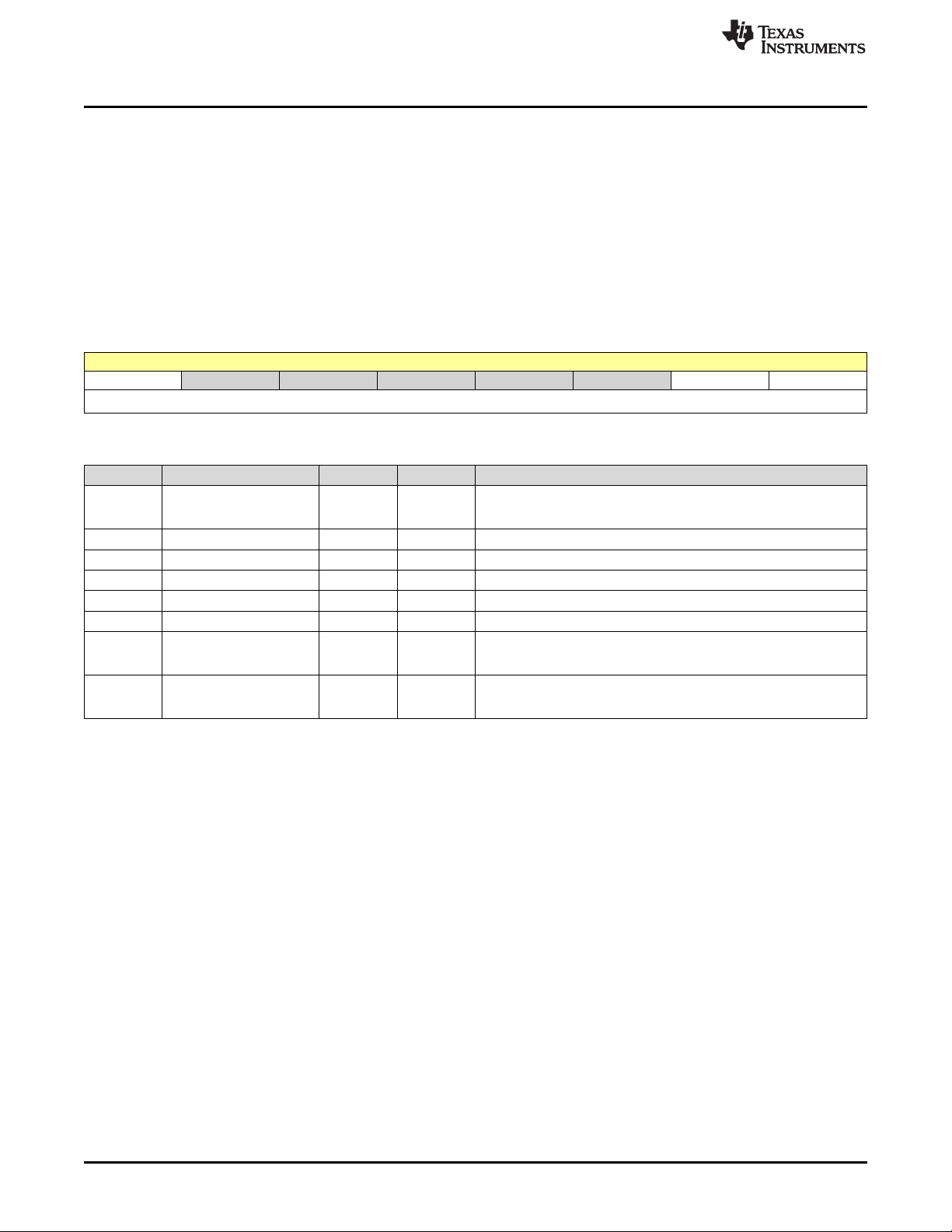
FUNC_LDO Registers
3.4.11 LDO_PD_CTRL1 Register (Address = 16Bh) [reset = 83h]
LDO_PD_CTRL1 is shown in Figure 3-47 and described in Table 3-51.
Return to Summary Table.
LDO Pull-Down enable register #1
RESET register domain: HWRST
NOTES:
LDO pull-down enable register bits validate the control of the active discharge of each power resource to
fulfill the turn-off timing requirements.
When a pull-down is not enabled, there is always a weak pull-down present at the output of the power
resource, so that the device restarts correctly at the next power-up sequence.
Figure 3-47. LDO_PD_CTRL1 Register
7 6 5 4 3 2 1 0
LDO4 RESERVED RESERVED RESERVED RESERVED RESERVED LDO2 LDO1
R/W-1h R-0h R-0h R-0h R-0h R-0h R/W-1h R/W-1h
Table 3-51. LDO_PD_CTRL1 Register Field Descriptions
Bit Field Type Reset Description
7 LDO4 R/W 1h
6 RESERVED R 0h
5 RESERVED R 0h
4 RESERVED R 0h
3 RESERVED R 0h
2 RESERVED R 0h
1 LDO2 R/W 1h
0 LDO1 R/W 1h
0: Pull-Down is disable
1: Pull-Down is enabled when LDO4 is in OFF state
0: Pull-Down is disable
1: Pull-Down is enabled when LDO2 is in OFF state
0: Pull-Down is disable
1: Pull-Down is enabled when LDO1 is in OFF state
www.ti.com
58
Register Descriptions
Copyright © 2015–2017, Texas Instruments Incorporated
SLVUAH1C–June 2015–Revised April 2017
Submit Documentation Feedback
Page 59
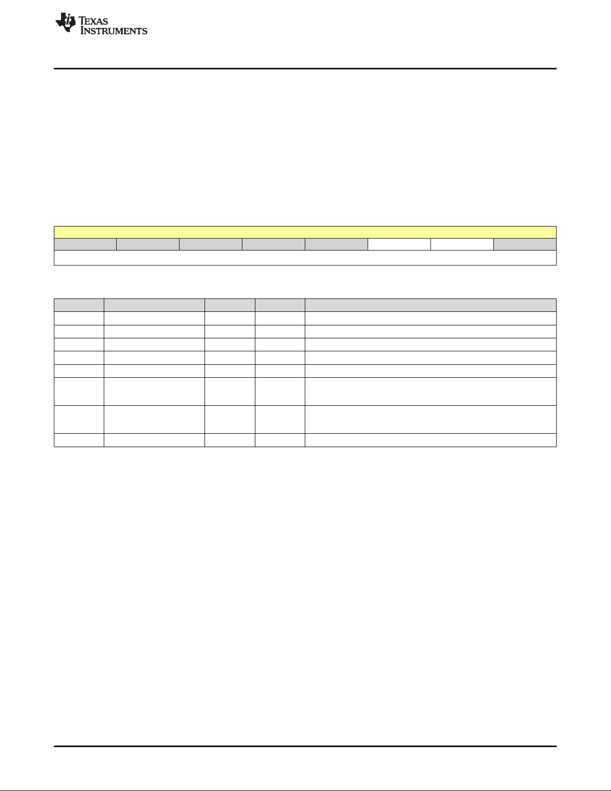
www.ti.com
FUNC_LDO Registers
3.4.12 LDO_PD_CTRL2 Register (Address = 16Ch) [reset = 6h]
LDO_PD_CTRL2 is shown in Figure 3-48 and described in Table 3-52.
Return to Summary Table.
LDO Pull-Down enable register #2
RESET register domain: HWRST
NOTES:
LDO pull-down enable register bits validate the control of the active discharge of each power resource to
fulfill the turn-off timing requirements.
When a pull-down is not enabled, there is always a weak pull-down present at the output of the power
resource, so that the device restarts correctly at the next power-up sequence.
Figure 3-48. LDO_PD_CTRL2 Register
7 6 5 4 3 2 1 0
RESERVED RESERVED RESERVED RESERVED RESERVED LDO3 LDO5 RESERVED
R-0h R-0h R-0h R-0h R-0h R/W-1h R/W-1h R-0h
Table 3-52. LDO_PD_CTRL2 Register Field Descriptions
Bit Field Type Reset Description
7 RESERVED R 0h
6 RESERVED R 0h
5 RESERVED R 0h
4 RESERVED R 0h
3 RESERVED R 0h
2 LDO3 R/W 1h
1 LDO5 R/W 1h
0 RESERVED R 0h
0: Pull-Down is disable
1: Pull-Down is enabled when LDOUSB is in OFF state
0: Pull-Down is disable
1: Pull-Down is enabled when LDOLN is in OFF state
SLVUAH1C–June 2015–Revised April 2017
Submit Documentation Feedback
Copyright © 2015–2017, Texas Instruments Incorporated
Register Descriptions
59
Page 60

FUNC_LDO Registers
3.4.13 LDO_SHORT_STATUS1 Register (Address = 16Dh) [reset = 0h]
LDO_SHORT_STATUS1 is shown in Figure 3-49 and described in Table 3-53.
Return to Summary Table.
LDO Short circuit status register #1
At Power-On, LDO short input informations are masked during 1 ms. This 1 ms masking is activated and
re-started each time one LDO is enabled.
RESET register domain: POR
Figure 3-49. LDO_SHORT_STATUS1 Register
7 6 5 4 3 2 1 0
LDO4 RESERVED RESERVED RESERVED RESERVED RESERVED LDO2 LDO1
R-0h R-0h R-0h R-0h R-0h R-0h R-0h R-0h
Table 3-53. LDO_SHORT_STATUS1 Register Field Descriptions
Bit Field Type Reset Description
7 LDO4 R 0h
6 RESERVED R 0h
5 RESERVED R 0h
4 RESERVED R 0h
3 RESERVED R 0h
2 RESERVED R 0h
1 LDO2 R 0h
0 LDO1 R 0h
0: LDO4 is functional. No short detected (default)
1: LDO4 output is short detected
0: LDO2 is functional. No short detected (default)
1: LDO2 output is short detected
0: LDO1 is functional. No short detected (default)
1: LDO1 output is short detected
www.ti.com
60
Register Descriptions
Copyright © 2015–2017, Texas Instruments Incorporated
SLVUAH1C–June 2015–Revised April 2017
Submit Documentation Feedback
Page 61

www.ti.com
FUNC_LDO Registers
3.4.14 LDO_SHORT_STATUS2 Register (Address = 16Eh) [reset = 0h]
LDO_SHORT_STATUS2 is shown in Figure 3-50 and described in Table 3-54.
Return to Summary Table.
LDO short circuit status register #2
RESET register domain: POR
Figure 3-50. LDO_SHORT_STATUS2 Register
7 6 5 4 3 2 1 0
RESERVED RESERVED RESERVED RESERVED RESERVED LDO3 LDO5 RESERVED
R-0h R-0h R-0h R-0h R-0h R-0h R-0h R-0h
Table 3-54. LDO_SHORT_STATUS2 Register Field Descriptions
Bit Field Type Reset Description
7 RESERVED R 0h
6 RESERVED R 0h
5 RESERVED R 0h
4 RESERVED R 0h
3 RESERVED R 0h
2 LDO3 R 0h
1 LDO5 R 0h
0 RESERVED R 0h
0: LDOUSB is functional. No short detected (default)
1: LDOUSB output is short detected
0: LDOLN is functional. No short detected (default)
1: LDOLN output is short detected
SLVUAH1C–June 2015–Revised April 2017
Submit Documentation Feedback
Copyright © 2015–2017, Texas Instruments Incorporated
Register Descriptions
61
Page 62
FUNC_LDO Registers
www.ti.com
3.4.15 LDO_PD_CTRL3 Register (Address = 17Dh) [reset = 80h]
LDO_PD_CTRL3 is shown in Figure 3-51 and described in Table 3-55.
Return to Summary Table.
LDO Pull-Down enable register #3
RESET register domain: HWRST
NOTES:
LDO pull-down enable register bits validate the control of the active discharge of each power resource to
fulfill the turn-off timing requirements.
When a pull-down is not enabled, there is always a weak pull-down present at the output of the power
resource, so that the device restarts correctly at the next power-up sequence.
Figure 3-51. LDO_PD_CTRL3 Register
7 6 5 4 3 2 1 0
LDOVANA RESERVED RESERVED
R/W-1h R-0h R-0h
Table 3-55. LDO_PD_CTRL3 Register Field Descriptions
Bit Field Type Reset Description
7 LDOVANA R/W 1h
6-1 RESERVED R 0h
0 RESERVED R 0h
0: Pull-Down is disable
1: Pull-Down is enabled when LDOVANA is in OFF state
62
Register Descriptions
Copyright © 2015–2017, Texas Instruments Incorporated
SLVUAH1C–June 2015–Revised April 2017
Submit Documentation Feedback
Page 63
www.ti.com
FUNC_LDO Registers
3.4.16 LDO_SHORT_STATUS3 Register (Address = 17Eh) [reset = 0h]
LDO_SHORT_STATUS3 is shown in Figure 3-52 and described in Table 3-56.
Return to Summary Table.
LDO short circuit status register #3
RESET register domain: POR
Figure 3-52. LDO_SHORT_STATUS3 Register
7 6 5 4 3 2 1 0
LDOVANA RESERVED RESERVED
R-0h R-0h R-0h
Table 3-56. LDO_SHORT_STATUS3 Register Field Descriptions
Bit Field Type Reset Description
7 LDOVANA R 0h
6-1 RESERVED R 0h
0 RESERVED R 0h
LDOVANA (internal LDO - reserved)
0: LDOVANA is functional. No short detected (default)
1: LDOVANA output is short detected
SLVUAH1C–June 2015–Revised April 2017
Submit Documentation Feedback
Copyright © 2015–2017, Texas Instruments Incorporated
Register Descriptions
63
Page 64

FUNC_SPI Registers
3.5 FUNC_SPI Registers
Table 3-57 lists the memory-mapped registers for the FUNC_SPI. All register offset addresses not listed in
Table 3-57 should be considered as reserved locations and the register contents should not be modified.
Table 3-57. FUNC_SPI Registers
Address Acronym Register Name Section
17Fh SPI_PAGE_CTRL SPI Page Control register (used only when SPI interface
is used).
RESET register domain: SWORST
Section 3.5.1
www.ti.com
64
Register Descriptions
Copyright © 2015–2017, Texas Instruments Incorporated
SLVUAH1C–June 2015–Revised April 2017
Submit Documentation Feedback
Page 65

www.ti.com
3.5.1 SPI_PAGE_CTRL Register (Address = 17Fh) [reset = 0h]
SPI_PAGE_CTRL is shown in Figure 3-53 and described in Table 3-58.
Return to Summary Table.
SPI Page Control register (used only when SPI interface is used).
RESET register domain: SWORST
Figure 3-53. SPI_PAGE_CTRL Register
7 6 5 4 3 2 1 0
RESERVED SPI_PAGE_AC
R-0h R/W-0h
Table 3-58. SPI_PAGE_CTRL Register Field Descriptions
Bit Field Type Reset Description
7-1 RESERVED R 0h
0 SPI_PAGE_ACCESS R/W 0h
Page selection for SPI interface only
0: page1 (ID1=48) and page2 (ID2=49)
1: page1 (ID1=48) and page3 (ID2=4A)
FUNC_SPI Registers
CESS
SLVUAH1C–June 2015–Revised April 2017
Submit Documentation Feedback
Copyright © 2015–2017, Texas Instruments Incorporated
Register Descriptions
65
Page 66

FUNC_DVFS Registers
3.6 FUNC_DVFS Registers
Table 3-59 lists the memory-mapped registers for the FUNC_DVFS. All register offset addresses not listed
in Table 3-59 should be considered as reserved locations and the register contents should not be
modified.
Table 3-59. FUNC_DVFS Registers
Address Acronym Register Name Section
180h SMPS_DVFS_CTRL SMPS DVFS control register
RESET register domain: SWORST (excepted
DVFS_SMPS_SELECT (bit 4) on POR)
181h SMPS_DVFS_VOLTAGE_MAX SMPS DVFS maximum voltage register
RESET register domain: HWRST
182h SMPS_DVFS_STATUS SMPS DVFS status register
RESET register domain: HWRST
Section 3.6.1
Section 3.6.2
Section 3.6.3
www.ti.com
66
Register Descriptions
Copyright © 2015–2017, Texas Instruments Incorporated
SLVUAH1C–June 2015–Revised April 2017
Submit Documentation Feedback
Page 67
www.ti.com
3.6.1 SMPS_DVFS_CTRL Register (Address = 180h) [reset = 4h]
SMPS_DVFS_CTRL is shown in Figure 3-54 and described in Table 3-60.
Return to Summary Table.
SMPS DVFS control register
RESET register domain: SWORST (excepted DVFS_SMPS_SELECT (bit 4) on POR)
Figure 3-54. SMPS_DVFS_CTRL Register
7 6 5 4 3 2 1 0
RESERVED DVFS_SMPS_
SELECT
R-0h R/W-0h R/W-0h R/W-1h R/W-0h R/W-0h
Table 3-60. SMPS_DVFS_CTRL Register Field Descriptions
Bit Field Type Reset Description
7-5 RESERVED R 0h
4 DVFS_SMPS_SELECT R/W 0h
3 DVFS_RESTORE_VALUER/W 0h
2 DVFS_ENABLE_RST R/W 1h
1 DVFS_OFFSET_STEP R/W 0h
0 DVFS_ENABLE R/W 0h
DVFS_RESTO
RE_VALUE
DVFS (I2C2_SCL, I2C2_SDA) SMPS selection
0: DVFS will control SMPS1(if single phase selected
SMPS_CTRL.SMPS12_SMPS1_SMPS2_EN=0) or SMPS12 (dualphase selected SMPS_CTRL.SMPS12_SMPS1_SMPS2_EN=1)
1: DVFS will control SMPS2(if single phase selected
SMPS_CTRL.SMPS12_SMPS1_SMPS2_EN=0) or SMPS12 (dualphase selected SMPS_CTRL.SMPS12_SMPS1_SMPS2_EN=1)
Note: The reset of this bit is on POR
Control the SMPS12 output voltage upon OFF to ACTIVE transition
controlled with ENABLE2 pins
0: upon OFF to ACTIVE transition controlled with ENABLE2 pins,
SMPS12 output voltage is set by SMPS12_VOLTAGE.VSEL register
1: upon OFF to ACTIVE transition controlled with ENABLE2 pins,
SMPS12 output voltage is set with the latest voltage (sum result of
the Offset value computed on PWM_DAT signal plus
SMPS12_FORCE.VSEL register) before ACTIVE to OFF. This value
is restored only if DVFS feature was already enabled
(DVFS_ENABLE=1) before ACTIVE to OFF transition controlled with
ENABLE2 pin.
Control the DVFS Enable feature upon OFF to ACTIVE transition
controlled with ENABLE2 pin.
0: DVFS feature is automatically re-enabled upon OFF to ACTIVE
transition controlled with ENABLE2 pin if the feature was already
enabled ((DVFS_ENABLE=1) before ACTIVE to OFF transition
controlled with ENABLE2 pin
1: DVFS feature is not automatically enable (DVFS_ENABLE=0)
upon OFF to ACTIVE transition controlled with ENABLE2 pin. To
select the DVFS feature, the DVFS_ENABLE must be written to one
by SW
Selection of the offset step for DVFS function:
0: offset step of 10mV (default)
1: offset step of 20mV
Selection of the DVFS function:
0: DVFS is not enabled (default)
1: DVFS is enabled (Control of SMPS12)
DVFS function in link to I2C2_SCL and I2C2_SDA.
DVFS_ENABL
E_RST
DVFS_OFFSE
T_STEP
FUNC_DVFS Registers
DVFS_ENABL
E
SLVUAH1C–June 2015–Revised April 2017
Submit Documentation Feedback
Copyright © 2015–2017, Texas Instruments Incorporated
Register Descriptions
67
Page 68

FUNC_DVFS Registers
3.6.2 SMPS_DVFS_VOLTAGE_MAX Register (Address = 181h) [reset = 0h]
SMPS_DVFS_VOLTAGE_MAX is shown in Figure 3-55 and described in Table 3-61.
Return to Summary Table.
SMPS DVFS maximum voltage register
RESET register domain: HWRST
Figure 3-55. SMPS_DVFS_VOLTAGE_MAX Register
7 6 5 4 3 2 1 0
LOCK VOLTAGE_MAX
R/W-0h R/W-0h
Table 3-61. SMPS_DVFS_VOLTAGE_MAX Register Field Descriptions
Bit Field Type Reset Description
7 LOCK R/W 0h
6-0 VOLTAGE_MAX R/W 0h
Access protection of the DVFS1_VOLTAGE_MAX register
0: No protection. R/W access to these register bits
1: Protection of these registers (Read only). This bit will reset (0b0)
during HWRST SWITCH-OFF
See VSEL cross table showed in SMPS12_VOLTAGE.VSEL register
with RANGE[0]=0 (x1 multiplier) and VSEL range from OFF, 0.5 to
1.65V
www.ti.com
68
Register Descriptions
Copyright © 2015–2017, Texas Instruments Incorporated
SLVUAH1C–June 2015–Revised April 2017
Submit Documentation Feedback
Page 69

www.ti.com
3.6.3 SMPS_DVFS_STATUS Register (Address = 182h) [reset = 0h]
SMPS_DVFS_STATUS is shown in Figure 3-56 and described in Table 3-62.
Return to Summary Table.
SMPS DVFS status register
RESET register domain: HWRST
Figure 3-56. SMPS_DVFS_STATUS Register
7 6 5 4 3 2 1 0
RESERVED OFFSET_STATUS
R-0h R-0h
Table 3-62. SMPS_DVFS_STATUS Register Field Descriptions
Bit Field Type Reset Description
7-6 RESERVED R 0h
5-0 OFFSET_STATUS R 0h
Offset status register (between 0 and 32 in decimal)
SMPS_DVFS_CTRL.DVFS1_OFFSET_STEP=0 (x1 multiplier, 10mv
per step)/ 1(x2 multiplier), 20mV per step)
000000: no offset
000001: 10mV/20mV
000010: 20mV/40mV
...
100000: 320mV/640mV
100001: reserved/reserved
..
111111: reserved/reserved
FUNC_DVFS Registers
SLVUAH1C–June 2015–Revised April 2017
Submit Documentation Feedback
Copyright © 2015–2017, Texas Instruments Incorporated
Register Descriptions
69
Page 70
FUNC_PMU_CONTROL Registers
3.7 FUNC_PMU_CONTROL Registers
Table 3-63 lists the memory-mapped registers for the FUNC_PMU_CONTROL. All register offset
addresses not listed in Table 3-63 should be considered as reserved locations and the register contents
should not be modified.
Table 3-63. FUNC_PMU_CONTROL Registers
Address Acronym Register Name Section
1A0h DEV_CTRL Device Control Register
RESET register domain: SWORST (excepted
OSC_FAILURE on POR)
1A1h POWER_CTRL Power control register
RESET register domain: SWORST
1A2h VSYS_LO VSYS Low threshold register
RESET register domain: HWRST
1A3h VSYS_MON VSYS Monitoring register.
This register is initialized by OTP memory (VSYS_HI from 2.5V to 3.85V only).
The software can overwrite this value by a new value
(VSYS_MON - from 2.3V to 4.6V).
RESET register domain: SWORST
1A5h WATCHDOG Watch dog timer Register
RESET register domain: SWORST
NOTES:
The WATCHDOG.TIMER counter is initialized with the
RESET_OUT=0
The WATCHDOG.TIMER counter starts as soon as
RESET_OUT is released.
1A8h VRTC_CTRL VRTC Control Register
RESET register domain: HWRST
1A9h LONG_PRESS_KEY Long Press Key (LPK) configuration register
RESET register domain: HWRST
1AAh OSC_THERM_CTRL Oscillator and Thermal control register
RESET register domain: HWRST
1AFh SWOFF_HWRST Qualify which switch off events generate a HW RESET
(configuration of behavior of the device)
RESET register domain: HWRST
1B0h SWOFF_COLDRST Qualify which switch off events generate a COLD
RESET (configuration of behavior of the device)
RESET register domain: HWRST
1B1h SWOFF_STATUS Status register: registers switch off event
RESET register domain: PORRST
1B2h PMU_CONFIG PMU configuration
RESET register domain: HWRST
1B3h PMU_CTRL2 Power Management Unit Control #2
RESET register domain: HWRST
1B5h PMU_SECONDARY_INT Configuration and status of the Secondary Interrupt
Handler
RESET register domain: HWRST
1B7h SW_REVISION Software (SW) revision register
RESET register domain: HWRST
1B9h PMU_SECONDARY_INT2 Configuration and status of the Secondary Interrupt
Handler (Register2)
RESET register domain: HWRST
1C3h BOOT_STATUS Boot Status Register
RESET register domain: POR
Section 3.7.1
Section 3.7.2
Section 3.7.3
Section 3.7.4
Section 3.7.5
Section 3.7.6
Section 3.7.7
Section 3.7.8
Section 3.7.9
Section 3.7.10
Section 3.7.11
Section 3.7.12
Section 3.7.13
Section 3.7.14
Section 3.7.15
Section 3.7.16
Section 3.7.17
www.ti.com
70
Register Descriptions
Copyright © 2015–2017, Texas Instruments Incorporated
SLVUAH1C–June 2015–Revised April 2017
Submit Documentation Feedback
Page 71

www.ti.com
FUNC_PMU_CONTROL Registers
3.7.1 DEV_CTRL Register (Address = 1A0h) [reset = 1h]
DEV_CTRL is shown in Figure 3-57 and described in Table 3-64.
Return to Summary Table.
Device Control Register
RESET register domain: SWORST (excepted OSC_FAILURE on POR)
Figure 3-57. DEV_CTRL Register
7 6 5 4 3 2 1 0
RESERVED DEV_STATUS SW_RST DEV_ON
R-0h R-0h R/W-0h R/W-1h
Table 3-64. DEV_CTRL Register Field Descriptions
Bit Field Type Reset Description
7-4 RESERVED R 0h
3-2 DEV_STATUS R 0h
1 SW_RST R/W 0h
0 DEV_ON R/W 1h
Device status
00: OFF
01: ACTIVE
10: Not applicable (ACTIVE)
11: SLEEP
Software Reset (SW_RST)
Writing 1 will restart the device (turn-off sequence followed by turn-
on sequence)
This bit is cleared automatically
Device ON enable
1: will maintain the device in ACTIVE mode
0: allow the device to go in OFF mode
SLVUAH1C–June 2015–Revised April 2017
Submit Documentation Feedback
Copyright © 2015–2017, Texas Instruments Incorporated
Register Descriptions
71
Page 72

FUNC_PMU_CONTROL Registers
3.7.2 POWER_CTRL Register (Address = 1A1h) [reset = 7h]
POWER_CTRL is shown in Figure 3-58 and described in Table 3-65.
Return to Summary Table.
Power control register
RESET register domain: SWORST
Figure 3-58. POWER_CTRL Register
7 6 5 4 3 2 1 0
RESERVED ENABLE2_MASKENABLE1_MASKNSLEEP_MAS
R-0h R/W-1h R/W-1h R/W-1h
Table 3-65. POWER_CTRL Register Field Descriptions
Bit Field Type Reset Description
7-3 RESERVED R 0h
2 ENABLE2_MASK R/W 1h
1 ENABLE1_MASK R/W 1h
0 NSLEEP_MASK R/W 1h
Enable of the ENABLE2 line (mask)
0: ENABLE2 is not masked (allow control of the resource with
ENABLE2 pin)
1: ENABLE2 is masked (does not affect resource control) (default)
Enable of the ENABLE1 line (mask)
0: ENABLE1 is not masked (allow control of the resource with
ENABLE1 pin)
1: ENABLE1 is masked (does not affect resource control) (default)
Enable of the NSLEEP line (mask)
0: NSLEEP is not masked (allow control of the resource with
NSLEEP pin)
1: NSLEEP is masked (does not affect resource control) (default)
www.ti.com
K
72
Register Descriptions
Copyright © 2015–2017, Texas Instruments Incorporated
SLVUAH1C–June 2015–Revised April 2017
Submit Documentation Feedback
Page 73

www.ti.com
FUNC_PMU_CONTROL Registers
3.7.3 VSYS_LO Register (Address = 1A2h) [reset = X]
VSYS_LO is shown in Figure 3-59 and described in Table 3-66.
Return to Summary Table.
VSYS Low threshold register
RESET register domain: HWRST
Figure 3-59. VSYS_LO Register
7 6 5 4 3 2 1 0
RESERVED THRESHOLD
R-0h R-X
Table 3-66. VSYS_LO Register Field Descriptions
Bit Field Type Reset Description
7-5 RESERVED R 0h
4-0 THRESHOLD R X
VSYS_LO - System voltage falling edge threshold. When VCCx
input falls below VSYS_LO, device enters OFF mode and is ready
for start-up event.
Configured by OTP bits. From 2.5V to 3.10V per 50mV step.
00000 = 2.300 V (Reserved)
00001 = 2.050 V (Reserved)
00010 = 2.100 V (Reserved)
00011 = 2.150 V (Reserved)
00100 = 2.200 V (Reserved)
00101 = 2.250 V (Reserved)
00110 = 2.300 V (Reserved)
00111 = 2.350 V (Reserved)
01000 = 2.400 V (Reserved)
01001 = 2.450 V (Reserved)
01010 = 2.500 V
01011 = 2.550 V
01100 = 2.600 V
01101 = 2.650 V
01110 = 2.700 V
01111 = 2.750 V
10000 = 2.800 V
10001 = 2.850 V
10010 = 2.900 V
10011 = 2.950 V
10100 = 3.000 V
10101 = 3.050 V
10110 = 3.100V
10111 = Reserved
..
11111 = Reserved
SLVUAH1C–June 2015–Revised April 2017
Submit Documentation Feedback
Copyright © 2015–2017, Texas Instruments Incorporated
Register Descriptions
73
Page 74
FUNC_PMU_CONTROL Registers
3.7.4 VSYS_MON Register (Address = 1A3h) [reset = X]
VSYS_MON is shown in Figure 3-60 and described in Table 3-67.
Return to Summary Table.
VSYS Monitoring register. This register is initialized by OTP memory (VSYS_HI - from 2.5V to 3.85V only).
The software can overwrite this value by a new value (VSYS_MON - from 2.3V to 4.6V).
RESET register domain: SWORST
Figure 3-60. VSYS_MON Register
7 6 5 4 3 2 1 0
ENABLE RESERVED THRESHOLD
R/W-0h R-0h R/W-X
Table 3-67. VSYS_MON Register Field Descriptions
Bit Field Type Reset Description
7 ENABLE R/W 0h
6 RESERVED R 0h
Enable VSYS monitoring (only in ACTIVE /SLEEP)
0: VSYS monitoring is not enabled
1: VSYS monitoring is enabled
www.ti.com
74
Register Descriptions
Copyright © 2015–2017, Texas Instruments Incorporated
SLVUAH1C–June 2015–Revised April 2017
Submit Documentation Feedback
Page 75
www.ti.com
Table 3-67. VSYS_MON Register Field Descriptions (continued)
Bit Field Type Reset Description
5-0 THRESHOLD R/W X
FUNC_PMU_CONTROL Registers
VSYS_HI
Configured by OTP bits (from 2.5V to 3.85V). By SW, from 2.3V to
4.6V per 50mV step.
000000 = 2.30 V 100000 = 3.60 V
000001 = 2.30 V 100001 = 3.65 V
000010 = 2.30 V 100010 = 3.70 V
000011 = 2.30 V 100011 = 3.75 V
000100 = 2.30 V 100100 = 3.80 V
000101 = 2.30 V 100101 = 3.85 V
000110 = 2.30 V 100110 = 3.90 V
000111 = 2.35 V 100111 = 3.95 V
001000 = 2.40 V 101000 = 4.00 V
001001 = 2.45 V 101001 = 4.05 V
001010 = 2.50 V 101010 = 4.10 V
001011 = 2.55 V 101011 = 4.15 V
001100 = 2.60 V 101100 = 4.20 V
001101 = 2.65 V 101101 = 4.25 V
001110 = 2.70 V 101110 = 4.30 V
001111 = 2.75 V 101111 = 4.35 V
010000 = 2.80 V 110000 = 4.40 V
010001 = 2.85 V 110001 = 4.45 V
010010 = 2.90 V 110010 = 4.50 V
010011 = 2.95 V 110011 = 4.55 V
010100 = 3.00 V 110100 = 4.60 V
010101 = 3.05 V 110101 = 4.60 V
010110 = 3.10 V 110110 = 4.60 V
010111 = 3.15 V 110111 = 4.60 V
011000 = 3.20 V 111000 = 4.60 V
011001 = 3.25 V 111001 = 4.60 V
011010 = 3.30 V 111010 = 4.60 V
011011 = 3.35 V 111011 = 4.60 V
011100 = 3.40 V 111100 = 4.60 V
011101 = 3.45 V 111101 = 4.60 V
011110 = 3.50 V 111110 = 4.60 V
011111 = 3.55 V 111111 = 4.60 V
SLVUAH1C–June 2015–Revised April 2017
Submit Documentation Feedback
Copyright © 2015–2017, Texas Instruments Incorporated
Register Descriptions
75
Page 76

FUNC_PMU_CONTROL Registers
3.7.5 WATCHDOG Register (Address = 1A5h) [reset = 7h]
WATCHDOG is shown in Figure 3-61 and described in Table 3-68.
Return to Summary Table.
Watch dog timer Register
RESET register domain: SWORST
NOTES:
The WATCHDOG.TIMER counter is initialized with the RESET_OUT=0
The WATCHDOG.TIMER counter starts as soon as RESET_OUT is released.
Figure 3-61. WATCHDOG Register
7 6 5 4 3 2 1 0
RESERVED LOCK ENABLE MODE TIMER
R-0h R/W-0h R/W-0h R/W-0h R/W-7h
Table 3-68. WATCHDOG Register Field Descriptions
Bit Field Type Reset Description
7-6 RESERVED R 0h
5 LOCK R/W 0h
4 ENABLE R/W 0h
3 MODE R/W 0h
2-0 TIMER R/W 7h
Access protection of the WATCHDOG.ENABLE,
WATCHDOC.MODE and WATCHDOG.LOCK bits
0: No protection. R/W access to these register bits
1: Protection of these registers (Read only). This bit will reset (0b0)
during SWITCH-OFF
Selection of the Watchdog:
0: Watchdog is not selected (disable) (default)
1: Watchdog is elected (enabled)
Select type of watchdog behavior:
0: Periodic (default)
1: Interrupt mode
Timer delay selection:
000: 1s
001: 2s
010: 4s
011: 8s
100: 16s
101: 32s
110: 64s
111: 128s (default)
www.ti.com
76
Register Descriptions
Copyright © 2015–2017, Texas Instruments Incorporated
SLVUAH1C–June 2015–Revised April 2017
Submit Documentation Feedback
Page 77
www.ti.com
FUNC_PMU_CONTROL Registers
3.7.6 VRTC_CTRL Register (Address = 1A8h) [reset = X]
VRTC_CTRL is shown in Figure 3-62 and described in Table 3-69.
Return to Summary Table.
VRTC Control Register
RESET register domain: HWRST
Figure 3-62. VRTC_CTRL Register
7 6 5 4 3 2 1 0
VRTC_18_15 VRTC_EN_SLP VRTC_EN_OFFVRTC_PWEN RESERVED
R-X R/W-1h R/W-1h R/W-1h R-0h
Table 3-69. VRTC_CTRL Register Field Descriptions
Bit Field Type Reset Description
7 VRTC_18_15 R X
6 VRTC_EN_SLP R/W 1h
5 VRTC_EN_OFF R/W 1h
4 VRTC_PWEN R/W 1h
3-0 RESERVED R 0h
VRTC voltage selection. This bit will allow to decrease the power
consumption in BACKUP mode by setting the VRTC at 1.5V.
0: 1.8V (default)
1: 1.5V
0: VRTC is configured in the standard power mode configuration
when device is in SLEEP state (biasing also in SLEEP state).
1: VRTC is configured in a low-power mode configuration when
device is in SLEEP state (biasing also in SLEEP state) (default).
0: VRTC is configured in the standard power mode configuration
when device is in OFF state (biasing also in OFF state)
1: VRTC is configured in a low-power mode configuration when
device is in OFF state (biasing also in OFF state) (default).
0: VRTC is configured in a low-power mode configuration.
1: VRTC is configured in the standard power mode configuration
(default)
SLVUAH1C–June 2015–Revised April 2017
Submit Documentation Feedback
Copyright © 2015–2017, Texas Instruments Incorporated
Register Descriptions
77
Page 78
FUNC_PMU_CONTROL Registers
3.7.7 LONG_PRESS_KEY Register (Address = 1A9h) [reset = 3Ch]
LONG_PRESS_KEY is shown in Figure 3-63 and described in Table 3-70.
Return to Summary Table.
Long Press Key (LPK) configuration register
RESET register domain: HWRST
Figure 3-63. LONG_PRESS_KEY Register
7 6 5 4 3 2 1 0
LPK_LOCK RESERVED RESERVED RESERVED LPK_TIME RESERVED
R/W-0h R-0h R-1h R-1h R/W-3h R-0h
Table 3-70. LONG_PRESS_KEY Register Field Descriptions
Bit Field Type Reset Description
7 LPK_LOCK R/W 0h
6 RESERVED R 0h
5 RESERVED R 1h
4 RESERVED R 1h
3-2 LPK_TIME R/W 3h
1-0 RESERVED R 0h
Access protection of the LPK_TIME, LPK_EN and LPK_LOCK
registers
0: No protection. R/W access to these register bits (default)
1: Protection of these registers (Read only). This bit will reset (0b0)
during SWITCH-OFF
Long press key duration
00: 6 second
01: 8 second
10: 10 second
11: 4 second (default)
www.ti.com
78
Register Descriptions
Copyright © 2015–2017, Texas Instruments Incorporated
SLVUAH1C–June 2015–Revised April 2017
Submit Documentation Feedback
Page 79
www.ti.com
FUNC_PMU_CONTROL Registers
3.7.8 OSC_THERM_CTRL Register (Address = 1AAh) [reset = Ch]
OSC_THERM_CTRL is shown in Figure 3-64 and described in Table 3-71.
Return to Summary Table.
Oscillator and Thermal control register
RESET register domain: HWRST
Figure 3-64. OSC_THERM_CTRL Register
7 6 5 4 3 2 1 0
VANA_ON_IN_
SLEEP
R/W-0h R/W-0h R/W-0h R/W-0h R/W-3h R-0h R-0h
Bit Field Type Reset Description
7 VANA_ON_IN_SLEEP R/W 0h
6 INT_MASK_IN_SLEEP R/W 0h
5 RC15MHZ_ON_IN_SLEEPR/W 0h
4 THERM_OFF_IN_SLEEP R/W 0h
3-2 THERM_HD_SEL R/W 3h
1 RESERVED R 0h
0 RESERVED R 0h
INT_MASK_IN_
SLEEP
RC15MHZ_ON
_IN_SLEEP
THERM_OFF_I
N_SLEEP
THERM_HD_SEL RESERVED RESERVED
Table 3-71. OSC_THERM_CTRL Register Field Descriptions
0: VANA LDO is OFF in SLEEP mode (default)
1: VANA LDO is ON in SLEEP mode (In case some modules are
used in SLEEP mode and need VANA (ILMON))
INT masked selection during SLEEP mode (Released interrupt line
only when DEVICE fully wake up)
0: INT is not masked in SLEEP mode (default)
1: INT is asserted when SLEEP2ACTIVE transition is completed
(allow to wakeup platform before INT generation)
RC15MHZ oscillator selection during SLEEP mode
0: RC15MHZ oscillator is OFF in SLEEP mode. Minimize
consumption in SLEEP mode (default)
1: RC15MHZ oscillator is ON in SLEEP mode. It allow to make
I2C/SPI access in SLEEP mode.
THERM selection during SLEEP mode (Minimization of the power
consumption)
0: THERM is ON in SLEEP mode (default)
1: THERM is OFF in SLEEP mode
Hot die temperature detection selection:
00: 117 / 108 deg.
01: 121 / 112 deg.
10: 125 / 116 deg.
11: 130 / 120 deg. (default)
SLVUAH1C–June 2015–Revised April 2017
Submit Documentation Feedback
Copyright © 2015–2017, Texas Instruments Incorporated
Register Descriptions
79
Page 80

FUNC_PMU_CONTROL Registers
www.ti.com
3.7.9 SWOFF_HWRST Register (Address = 1AFh) [reset = X]
SWOFF_HWRST is shown in Figure 3-65 and described in Table 3-72.
Return to Summary Table.
Qualify which switch off events generate a HW RESET (configuration of behavior of the device)
RESET register domain: HWRST
Figure 3-65. SWOFF_HWRST Register
7 6 5 4 3 2 1 0
PWRON_LPK PWRDOWN WTD TSHUT RESET_IN SW_RST VSYS_LO GPADC_SHUT
R-X R-X R-X R-X R-X R-X R-X R-X
Table 3-72. SWOFF_HWRST Register Field Descriptions
Bit Field Type Reset Description
7 PWRON_LPK R X
6 PWRDOWN R X
5 WTD R X
4 TSHUT R X
3 RESET_IN R X
2 SW_RST R X
1 VSYS_LO R X
0 GPADC_SHUTDOWN R X
0: Masked (Switchoff reset)
1: Not masked (Hardware reset)
0: Masked (Switchoff reset)
1: Not masked (Hardware reset)
0: Masked (Switchoff reset)
1: Not masked (Hardware reset)
0: Masked (Switchoff reset)
1: Not masked (Hardware reset)
0: Masked (Switchoff reset)
1: Not masked (Hardware reset)
0: Masked (Switchoff reset)
1: Not masked (Hardware reset)
0: Masked (Switchoff reset)
1: Not masked (Hardware reset)
0: Masked (Switchoff reset)
1: Not masked (Hardware reset)
DOWN
80
Register Descriptions
Copyright © 2015–2017, Texas Instruments Incorporated
SLVUAH1C–June 2015–Revised April 2017
Submit Documentation Feedback
Page 81

www.ti.com
FUNC_PMU_CONTROL Registers
3.7.10 SWOFF_COLDRST Register (Address = 1B0h) [reset = X]
SWOFF_COLDRST is shown in Figure 3-66 and described in Table 3-73.
Return to Summary Table.
Qualify which switch off events generate a COLD RESET (configuration of behavior of the device)
RESET register domain: HWRST
Figure 3-66. SWOFF_COLDRST Register
7 6 5 4 3 2 1 0
PWRON_LPK PWRDOWN WTD TSHUT RESET_IN SW_RST VSYS_LO GPADC_SHUT
R/W-X R/W-X R/W-X R/W-X R/W-X R/W-X R/W-X R/W-X
Table 3-73. SWOFF_COLDRST Register Field Descriptions
Bit Field Type Reset Description
7 PWRON_LPK R/W X
6 PWRDOWN R/W X
5 WTD R/W X
4 TSHUT R/W X
3 RESET_IN R/W X
2 SW_RST R/W X
1 VSYS_LO R/W X
0 GPADC_SHUTDOWN R/W X
0: Masked (Shutdown)
1: Not masked (Cold restart)
0: Masked (Shutdown)
1: Not masked (Cold restart)
0: Masked (Shutdown)
1: Not masked (Cold restart)
0: Masked (Shutdown)
1: Not masked (Cold restart)
0: Masked (Shutdown)
1: Not masked (Cold restart)
0: Masked (Shutdown)
1: Not masked (Cold restart)
0: Masked (Shutdown)
1: Not masked (Cold restart)
0: Masked (Shutdown)
1: Not masked (Cold restart)
DOWN
SLVUAH1C–June 2015–Revised April 2017
Submit Documentation Feedback
Copyright © 2015–2017, Texas Instruments Incorporated
Register Descriptions
81
Page 82

FUNC_PMU_CONTROL Registers
www.ti.com
3.7.11 SWOFF_STATUS Register (Address = 1B1h) [reset = 0h]
SWOFF_STATUS is shown in Figure 3-67 and described in Table 3-74.
Return to Summary Table.
Status register: registers switch off event
RESET register domain: PORRST
Figure 3-67. SWOFF_STATUS Register
7 6 5 4 3 2 1 0
PWRON_LPK PWRDOWN WTD TSHUT RESET_IN SW_RST VSYS_LO GPADC_SHUT
RC-0h RC-0h RC-0h RC-0h RC-0h RC-0h RC-0h RC-0h
Table 3-74. SWOFF_STATUS Register Field Descriptions
Bit Field Type Reset Description
7 PWRON_LPK RC 0h
6 PWRDOWN RC 0h
5 WTD RC 0h
4 TSHUT RC 0h
3 RESET_IN RC 0h
2 SW_RST RC 0h
1 VSYS_LO RC 0h
0 GPADC_SHUTDOWN RC 0h
0: no GPADC_SHUTDOWN
1: GPADC_SHUTDOWN occured since last read of this register
DOWN
82
Register Descriptions
Copyright © 2015–2017, Texas Instruments Incorporated
SLVUAH1C–June 2015–Revised April 2017
Submit Documentation Feedback
Page 83

www.ti.com
FUNC_PMU_CONTROL Registers
3.7.12 PMU_CONFIG Register (Address = 1B2h) [reset = X]
PMU_CONFIG is shown in Figure 3-68 and described in Table 3-75.
Return to Summary Table.
PMU configuration
RESET register domain: HWRST
Figure 3-68. PMU_CONFIG Register
7 6 5 4 3 2 1 0
RESERVED HIGH_VCC_SE
NSE
R-0h R/W-X R/W-X R/W-X R-0h R/W-X
Bit Field Type Reset Description
7 RESERVED R 0h
6 HIGH_VCC_SENSE R/W X
5-4 PLL_AUTO_CTRL R/W X
3-2 SWOFF_DLY R/W X
1 RESERVED R 0h
0 AUTODEVON R/W X
PLL_AUTO_CTRL SWOFF_DLY RESERVED AUTODEVON
Table 3-75. PMU_CONFIG Register Field Descriptions
Enable input buffer for VCC_SENSE input to reduce input leakage.
Rrecommended when VCC_SENSE is >5V
0: VCC_SENSE input buffer is not enabled
1: VCC_SENSE input buffer is enabled
Enable/disable PLL under different device mode:
00 : PLL is not enabled/disabled automatically. PLL enable
command should be stored in OTP for power sequence.
01 : Enable PLL in ACTIVE mode at the start point of OFF2ACT
transition. Disabled at the end point of ACT2OFF.
10 : Enable PLL in SLEEP mode only.
11 : Enable PLL in both of ACTIVE mode and SLEEP mode at the
start point of OFF2ACT transition. Disabled at the end point of
ACT2OFF.
Delay before to go to SWITCH-OFF to allow host processor to save
his context (device will be maintained ACTIVE until delay expiration
then SWITCH-OFF)
00: no delay
01: 1 second window (+/- 250ms)
10: 2 second window (+/- 250ms)
11: 4 second window (+/- 250ms)
Selection of the feature Auto Device ON
0: Feature is inactive
1: Feature is active
SLVUAH1C–June 2015–Revised April 2017
Submit Documentation Feedback
Copyright © 2015–2017, Texas Instruments Incorporated
Register Descriptions
83
Page 84

FUNC_PMU_CONTROL Registers
3.7.13 PMU_CTRL2 Register (Address = 1B3h) [reset = X]
PMU_CTRL2 is shown in Figure 3-69 and described in Table 3-76.
Return to Summary Table.
Power Management Unit Control #2
RESET register domain: HWRST
Figure 3-69. PMU_CTRL2 Register
7 6 5 4 3 2 1 0
SPARE7 SPARE6 SPARE5 SPARE4 INT_LINE_DIS WDT_HOLD_I
R/W-X R/W-X R/W-X R/W-X R/W-X R/W-X R/W-X R/W-X
N_SLEEP
Table 3-76. PMU_CTRL2 Register Field Descriptions
Bit Field Type Reset Description
7 SPARE7 R/W X
6 SPARE6 R/W X
5 SPARE5 R/W X
4 SPARE4 R/W X
3 INT_LINE_DIS R/W X
2 WDT_HOLD_IN_SLEEP R/W X
1 PWRDOWN_FASTOFF R/W X
0 TSHUT_FASTOFF R/W X
Interrupt line (INT) output buffer configuration
0: Normal operation (standard buffer - OD or PP - )
1: INT output buffer is high-impedance with an internal pull-up to VIO
enabled
0: primary watchdog timer continues to run in device sleep state
1: primary watchdog timer is hold in device sleep state
0: PWRDOWN event triggers normal switch off sequence
1: PWRDOWN event triggers fast switch off sequence (all resources
disabeld together)
0: TSHUT event triggers normal switch off sequence
1: TSHUT event triggers fast switch off sequence (all resources
disabeld together)
PWRDOWN_F
ASTOFF
www.ti.com
TSHUT_FAST
OFF
84
Register Descriptions
Copyright © 2015–2017, Texas Instruments Incorporated
SLVUAH1C–June 2015–Revised April 2017
Submit Documentation Feedback
Page 85

www.ti.com
FUNC_PMU_CONTROL Registers
3.7.14 PMU_SECONDARY_INT Register (Address = 1B5h) [reset = X]
PMU_SECONDARY_INT is shown in Figure 3-70 and described in Table 3-77.
Return to Summary Table.
Configuration and status of the Secondary Interrupt Handler
RESET register domain: HWRST
Figure 3-70. PMU_SECONDARY_INT Register
7 6 5 4 3 2 1 0
RESERVED RESERVED RESERVED FSD_INT_SRC RESERVED RESERVED RESERVED FSD_MASK
R-0h R-0h R-0h RC-0h R-0h R-0h R-0h R/W-X
Table 3-77. PMU_SECONDARY_INT Register Field Descriptions
Bit Field Type Reset Description
7 RESERVED R 0h
6 RESERVED R 0h
5 RESERVED R 0h
4 FSD_INT_SRC RC 0h
3 RESERVED R 0h
2 RESERVED R 0h
1 RESERVED R 0h
0 FSD_MASK R/W X
First Supply Detection (FSD) interrupt status source
0: First Supply Detection (FSD) is not the source of interrupt line
BB_FSD
1: First Supply Detection (FSD) is the source of interrupt line
BB_FSD
Secondary level of mask for FSD_BB interrupt line. First Supply
Detection (FSD) Mask.
0: Un-masked
1: Masked
SLVUAH1C–June 2015–Revised April 2017
Submit Documentation Feedback
Copyright © 2015–2017, Texas Instruments Incorporated
Register Descriptions
85
Page 86

FUNC_PMU_CONTROL Registers
3.7.15 SW_REVISION Register (Address = 1B7h) [reset = X]
SW_REVISION is shown in Figure 3-71 and described in Table 3-78.
Return to Summary Table.
Software (SW) revision register
RESET register domain: HWRST
Figure 3-71. SW_REVISION Register
7 6 5 4 3 2 1 0
SW_REVISION
R-X
Table 3-78. SW_REVISION Register Field Descriptions
Bit Field Type Reset Description
7-0 SW_REVISION R X
Software (SW) revision register - This revision will be representative
of the OTP version.
www.ti.com
86
Register Descriptions
Copyright © 2015–2017, Texas Instruments Incorporated
SLVUAH1C–June 2015–Revised April 2017
Submit Documentation Feedback
Page 87

www.ti.com
FUNC_PMU_CONTROL Registers
3.7.16 PMU_SECONDARY_INT2 Register (Address = 1B9h) [reset = 0h]
PMU_SECONDARY_INT2 is shown in Figure 3-72 and described in Table 3-79.
Return to Summary Table.
Configuration and status of the Secondary Interrupt Handler (Register2)
RESET register domain: HWRST
Figure 3-72. PMU_SECONDARY_INT2 Register
7 6 5 4 3 2 1 0
RESERVED DVFS_INT_SR
RC-0h RC-0h R-0h R/W-0h
C
Table 3-79. PMU_SECONDARY_INT2 Register Field Descriptions
Bit Field Type Reset Description
7-5 RESERVED RC 0h
4 DVFS_INT_SRC RC 0h
3-1 RESERVED R 0h
0 DVFS_MASK R/W 0h
DVFS (Voltage plus offset over voltage max) interrupt status source
0: DVFS (Voltage plus offset over voltage max) is not the source of
interrupt line
1: DVFS (Voltage plus offset over voltage max) is the source of
interrupt line
Secondary level of mask for DVFS interrupt line. Voltage plus offset
over voltage max mask.
0: Un-masked
1: Masked
RESERVED DVFS_MASK
SLVUAH1C–June 2015–Revised April 2017
Submit Documentation Feedback
Copyright © 2015–2017, Texas Instruments Incorporated
Register Descriptions
87
Page 88

FUNC_PMU_CONTROL Registers
3.7.17 BOOT_STATUS Register (Address = 1C3h) [reset = X]
BOOT_STATUS is shown in Figure 3-73 and described in Table 3-80.
Return to Summary Table.
Configuration and status of the Boot Status Register. The boot mode is only latched during POR, and
should not be changed while the PMIC is supplied.
RESET register domain: POR
Figure 3-73. BOOT_STATUS Register
7 6 5 4 3 2 1 0
RESERVED BOOT_MODE
R-0h R-X
Table 3-80. BOOT_STATUS Register Field Descriptions
Bit Field Type Reset Description
7-1 RESERVED R 0h
0 BOOT_MODE R X
BOOT mode selection
0: BOOT pin is pulled low
1: BOOT pin is pulled high
www.ti.com
88
Register Descriptions
Copyright © 2015–2017, Texas Instruments Incorporated
SLVUAH1C–June 2015–Revised April 2017
Submit Documentation Feedback
Page 89
www.ti.com
FUNC_RESOURCE Registers
3.8 FUNC_RESOURCE Registers
Table 3-81 lists the memory-mapped registers for the FUNC_RESOURCE. All register offset addresses
not listed in Table 3-81 should be considered as reserved locations and the register contents should not
be modified.
Table 3-81. FUNC_RESOURCE Registers
Address Acronym Register Name Section
1D6h REGEN1_CTRL REGEN1 control register
RESET register domain: SWORST
1D7h PLLEN_CTRL PLLEN control register
RESET register domain: SWORST
1DAh NSLEEP_RES_ASSIGN NSLEEP resource assignment register
RESET register domain: HWRST
1DBh NSLEEP_SMPS_ASSIGN NSLEEP input signal SMPS resource assignment
register
RESET register domain: HWRST
1DCh NSLEEP_LDO_ASSIGN1 NSLEEP input signal LDO resource assignment register
#1
RESET register domain: HWRST
1DDh NSLEEP_LDO_ASSIGN2 NSLEEP input signal LDO resource assignment register
#2
RESET register domain: HWRST
1DEh ENABLE1_RES_ASSIGN ENABLE1 resource assignment register
RESET register domain: HWRST
1DFh ENABLE1_SMPS_ASSIGN ENABLE1 input signal SMPS resource assignment
register
RESET register domain: HWRST
1E0h ENABLE1_LDO_ASSIGN1 ENABLE1 input signal LDO resource assignment
register #1
RESET register domain: HWRST
1E1h ENABLE1_LDO_ASSIGN2 ENABLE1 input signal LDO resource assignment
register #2
RESET register domain: HWRST
1E2h ENABLE2_RES_ASSIGN ENABLE2 resource assignment register
RESET register domain: HWRST
1E3h ENABLE2_SMPS_ASSIGN ENABLE2 input signal SMPS resource assignment
register
RESET register domain: HWRST
1E4h ENABLE2_LDO_ASSIGN1 ENABLE2 input signal LDO resource assignment
register #1
RESET register domain: HWRST
1E5h ENABLE2_LDO_ASSIGN2 ENABLE2 input signal LDO resource assignment
register #2
RESET register domain: HWRST
1E6h REGEN2_CTRL REGEN2 control register
RESET register domain: SWORST
1E7h REGEN3_CTRL REGEN3 control register
RESET register domain: SWORST
Section 3.8.1
Section 3.8.2
Section 3.8.3
Section 3.8.4
Section 3.8.5
Section 3.8.6
Section 3.8.7
Section 3.8.8
Section 3.8.9
Section 3.8.10
Section 3.8.11
Section 3.8.12
Section 3.8.13
Section 3.8.14
Section 3.8.15
Section 3.8.16
SLVUAH1C–June 2015–Revised April 2017
Submit Documentation Feedback
Copyright © 2015–2017, Texas Instruments Incorporated
Register Descriptions
89
Page 90

FUNC_RESOURCE Registers
3.8.1 REGEN1_CTRL Register (Address = 1D6h) [reset = X]
REGEN1_CTRL is shown in Figure 3-74 and described in Table 3-82.
Return to Summary Table.
REGEN1 control register
RESET register domain: SWORST
Figure 3-74. REGEN1_CTRL Register
7 6 5 4 3 2 1 0
RESERVED STATUS RESERVED MODE_SLEEP RESERVED MODE_ACTIV
R-0h R-0h R-0h R/W-0h R-0h R/W-X
Table 3-82. REGEN1_CTRL Register Field Descriptions
Bit Field Type Reset Description
7-5 RESERVED R 0h
4 STATUS R 0h
3 RESERVED R 0h
2 MODE_SLEEP R/W 0h
1 RESERVED R 0h
0 MODE_ACTIVE R/W X
REGEN1 Status
0: OFF
1: ON
REGEN1 SLEEP Mode
0: OFF
1: ON
REGEN1 ACTIVE Mode (OTP-Sequencer)
0: OFF
1: ON
www.ti.com
E
90
Register Descriptions
Copyright © 2015–2017, Texas Instruments Incorporated
SLVUAH1C–June 2015–Revised April 2017
Submit Documentation Feedback
Page 91
www.ti.com
FUNC_RESOURCE Registers
3.8.2 PLLEN_CTRL Register (Address = 1D7h) [reset = 0h]
PLLEN_CTRL is shown in Figure 3-75 and described in Table 3-83.
Return to Summary Table.
PLLEN control register
RESET register domain: SWORST
Figure 3-75. PLLEN_CTRL Register
7 6 5 4 3 2 1 0
RESERVED STATUS RESERVED MODE_SLEEP RESERVED MODE_ACTIV
R-0h R-0h R-0h R/W-0h R-0h R/W-0h
Table 3-83. PLLEN_CTRL Register Field Descriptions
Bit Field Type Reset Description
7-5 RESERVED R 0h
4 STATUS R 0h
3 RESERVED R 0h
2 MODE_SLEEP R/W 0h
1 RESERVED R 0h
0 MODE_ACTIVE R/W 0h
PLLEN Status
0: OFF
1: ON
PLLEN SLEEP Mode
0: OFF
1: ON
PLLEN ACTIVE Mode (OTP-Sequencer)
0: OFF
1: ON
E
SLVUAH1C–June 2015–Revised April 2017
Submit Documentation Feedback
Copyright © 2015–2017, Texas Instruments Incorporated
Register Descriptions
91
Page 92

FUNC_RESOURCE Registers
3.8.3 NSLEEP_RES_ASSIGN Register (Address = 1DAh) [reset = 0h]
NSLEEP_RES_ASSIGN is shown in Figure 3-76 and described in Table 3-84.
Return to Summary Table.
NSLEEP resource assignment register
RESET register domain: HWRST
Figure 3-76. NSLEEP_RES_ASSIGN Register
7 6 5 4 3 2 1 0
RESERVED PLL_EN REGEN3 REGEN2 REGEN1
R-0h R/W-0h R/W-0h R/W-0h R/W-0h
Table 3-84. NSLEEP_RES_ASSIGN Register Field Descriptions
Bit Field Type Reset Description
7-4 RESERVED R 0h
3 PLL_EN R/W 0h
2 REGEN3 R/W 0h
1 REGEN2 R/W 0h
0 REGEN1 R/W 0h
0: NSLEEP has no effect on PLL_EN
1: PLL_EN is controlled by NSLEEP
0: NSLEEP has no effect on REGEN3
1: REGEN3 is controlled by NSLEEP
0: NSLEEP has no effect on REGEN2
1: REGEN2 is controlled by NSLEEP
0: NSLEEP has no effect on REGEN1
1: REGEN1 is controlled by NSLEEP
www.ti.com
92
Register Descriptions
Copyright © 2015–2017, Texas Instruments Incorporated
SLVUAH1C–June 2015–Revised April 2017
Submit Documentation Feedback
Page 93
www.ti.com
FUNC_RESOURCE Registers
3.8.4 NSLEEP_SMPS_ASSIGN Register (Address = 1DBh) [reset = 0h]
NSLEEP_SMPS_ASSIGN is shown in Figure 3-77 and described in Table 3-85.
Return to Summary Table.
NSLEEP input signal SMPS resource assignment register
RESET register domain: HWRST
Figure 3-77. NSLEEP_SMPS_ASSIGN Register
7 6 5 4 3 2 1 0
RESERVED SMPS5 RESERVED SMPS4 SMPS3 RESERVED SMPS2 SMPS1
R/W-0h R/W-0h R-0h R/W-0h R/W-0h R/W-0h R/W-0h R/W-0h
Table 3-85. NSLEEP_SMPS_ASSIGN Register Field Descriptions
Bit Field Type Reset Description
7 RESERVED R/W 0h
6 SMPS5 R/W 0h
5 RESERVED R 0h
4 SMPS4 R/W 0h
3 SMPS3 R/W 0h
2 RESERVED R/W 0h
1 SMPS2 R/W 0h
0 SMPS1 R/W 0h
0: NSLEEP has no effect on SMPS5
1: SMPS5 is controlled by NSLEEP
0: NSLEEP has no effect on SMPS4
1: SMPS4 is controlled by NSLEEP
0: NSLEEP has no effect on SMPS3
1: SMPS3 is controlled by NSLEEP
0: NSLEEP has no effect on SMPS2
1: SMPS2 is controlled by NSLEEP
0: NSLEEP has no effect on SMPS1 (or SMPS12 is dual phase
selected)
1: SMPS1 (or SMPS12 is dual phase selected) is controlled by
NSLEEP)
SLVUAH1C–June 2015–Revised April 2017
Submit Documentation Feedback
Copyright © 2015–2017, Texas Instruments Incorporated
Register Descriptions
93
Page 94
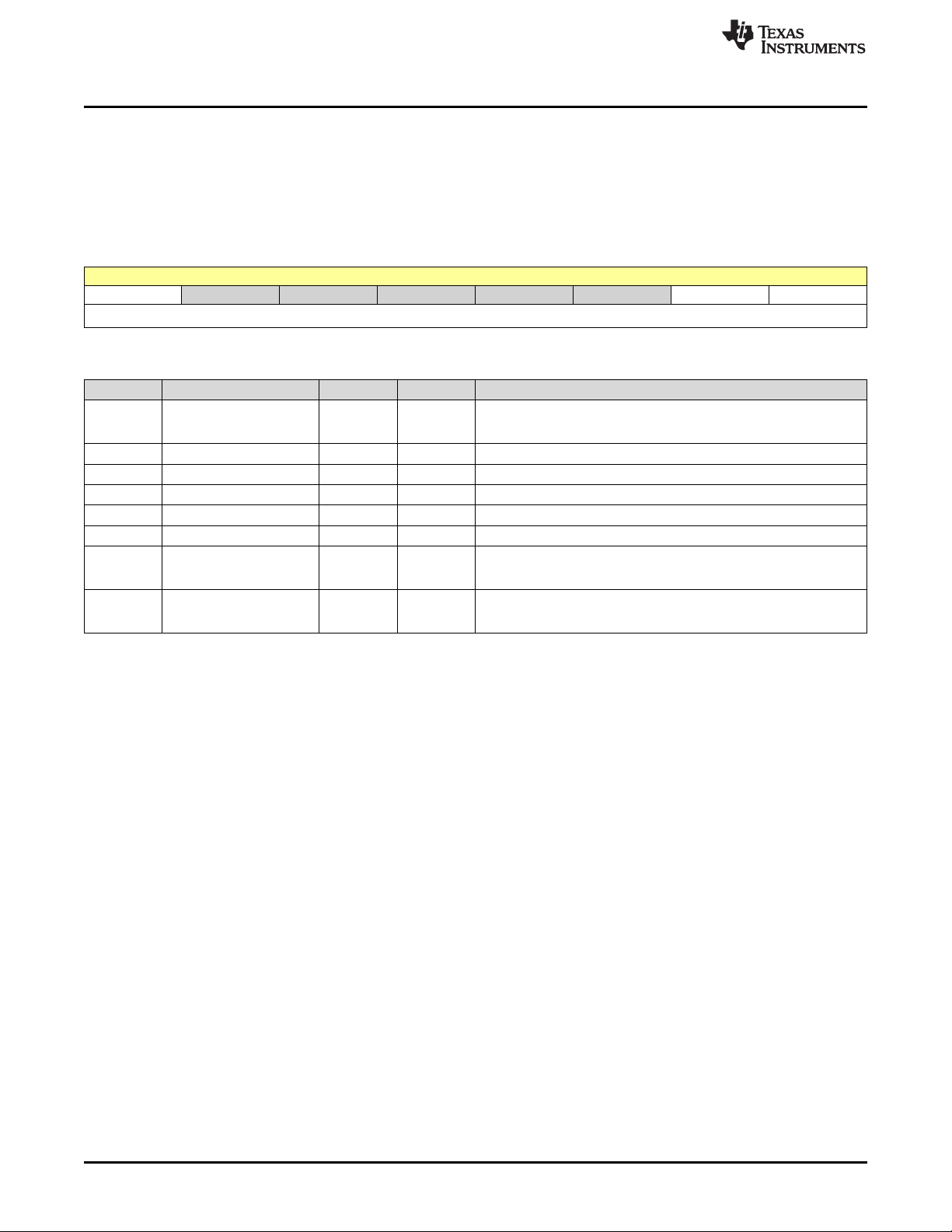
FUNC_RESOURCE Registers
3.8.5 NSLEEP_LDO_ASSIGN1 Register (Address = 1DCh) [reset = 0h]
NSLEEP_LDO_ASSIGN1 is shown in Figure 3-78 and described in Table 3-86.
Return to Summary Table.
NSLEEP input signal LDO resource assignment register #1
RESET register domain: HWRST
Figure 3-78. NSLEEP_LDO_ASSIGN1 Register
7 6 5 4 3 2 1 0
LDO4 RESERVED RESERVED RESERVED RESERVED RESERVED LDO2 LDO1
R/W-0h R-0h R-0h R-0h R/W-0h R-0h R/W-0h R/W-0h
Table 3-86. NSLEEP_LDO_ASSIGN1 Register Field Descriptions
Bit Field Type Reset Description
7 LDO4 R/W 0h
6 RESERVED R 0h
5 RESERVED R 0h
4 RESERVED R 0h
3 RESERVED R/W 0h
2 RESERVED R 0h
1 LDO2 R/W 0h
0 LDO1 R/W 0h
0: NSLEEP has no effect on LDO4
1: LDO4 is controlled by NSLEEP
0: NSLEEP has no effect on LDO2
1: LDO2 is controlled by NSLEEP
0: NSLEEP has no effect on LDO1
1: LDO1 is controlled by NSLEEP
www.ti.com
94
Register Descriptions
Copyright © 2015–2017, Texas Instruments Incorporated
SLVUAH1C–June 2015–Revised April 2017
Submit Documentation Feedback
Page 95
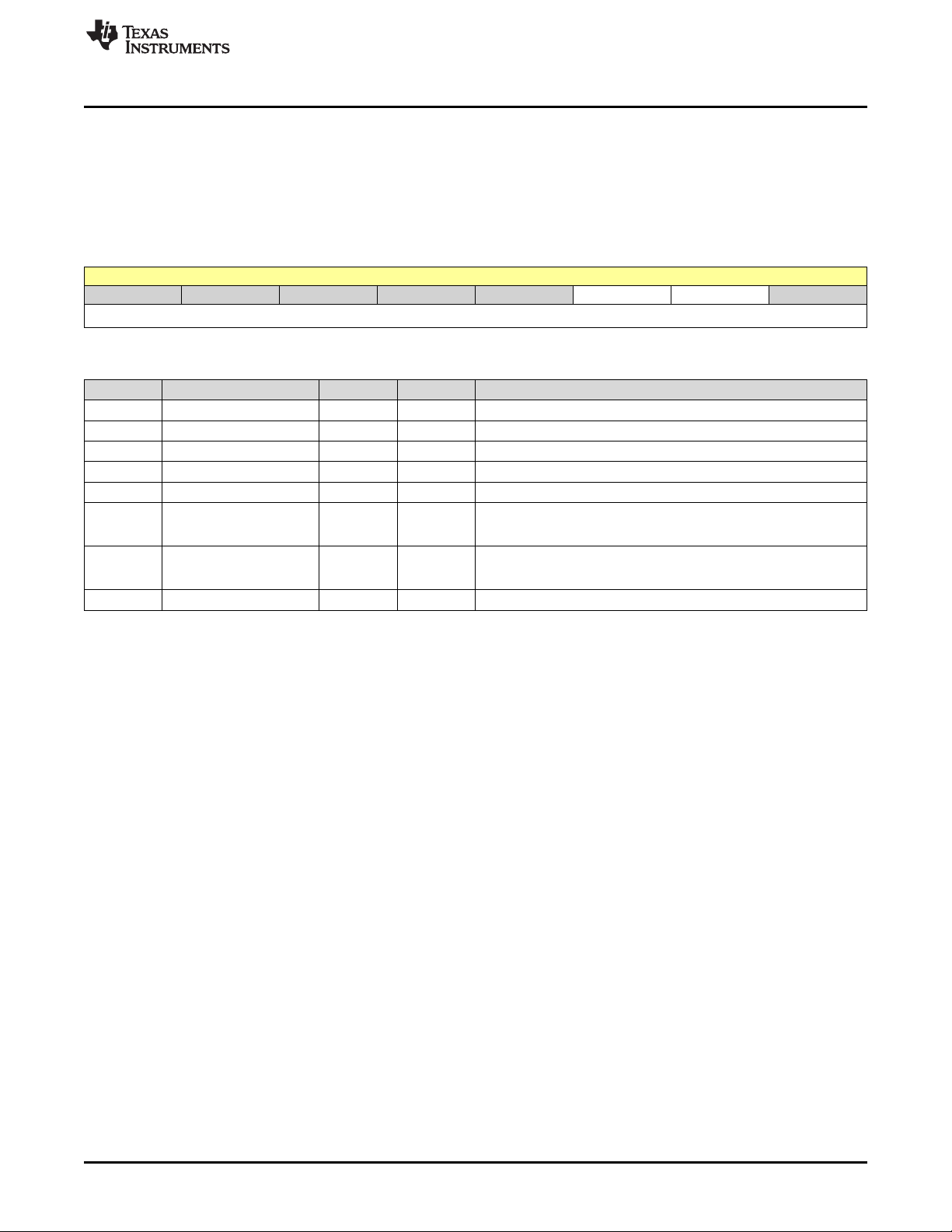
www.ti.com
FUNC_RESOURCE Registers
3.8.6 NSLEEP_LDO_ASSIGN2 Register (Address = 1DDh) [reset = 0h]
NSLEEP_LDO_ASSIGN2 is shown in Figure 3-79 and described in Table 3-87.
Return to Summary Table.
NSLEEP input signal LDO resource assignment register #2
RESET register domain: HWRST
Figure 3-79. NSLEEP_LDO_ASSIGN2 Register
7 6 5 4 3 2 1 0
RESERVED RESERVED RESERVED RESERVED RESERVED LDO3 LDO5 RESERVED
R-0h R-0h R-0h R-0h R-0h R/W-0h R/W-0h R-0h
Table 3-87. NSLEEP_LDO_ASSIGN2 Register Field Descriptions
Bit Field Type Reset Description
7 RESERVED R 0h
6 RESERVED R 0h
5 RESERVED R 0h
4 RESERVED R 0h
3 RESERVED R 0h
2 LDO3 R/W 0h
1 LDO5 R/W 0h
0 RESERVED R 0h
0: NSLEEP has no effect on LDO3
1: LDO3 is controlled by NSLEEP
0: NSLEEP has no effect on LDO5
1: LDO5 is controlled by NSLEEP
SLVUAH1C–June 2015–Revised April 2017
Submit Documentation Feedback
Copyright © 2015–2017, Texas Instruments Incorporated
Register Descriptions
95
Page 96

FUNC_RESOURCE Registers
3.8.7 ENABLE1_RES_ASSIGN Register (Address = 1DEh) [reset = 0h]
ENABLE1_RES_ASSIGN is shown in Figure 3-80 and described in Table 3-88.
Return to Summary Table.
ENABLE1 resource assignment register
RESET register domain: HWRST
Figure 3-80. ENABLE1_RES_ASSIGN Register
7 6 5 4 3 2 1 0
RESERVED PLL_EN REGEN3 REGEN2 REGEN1
R-0h R/W-0h R/W-0h R/W-0h R/W-0h
Table 3-88. ENABLE1_RES_ASSIGN Register Field Descriptions
Bit Field Type Reset Description
7-4 RESERVED R 0h
3 PLL_EN R/W 0h
2 REGEN3 R/W 0h
1 REGEN2 R/W 0h
0 REGEN1 R/W 0h
0: ENABLE1 has no effect on PLL_EN
1: PLL_EN is controlled by ENABLE1
0: ENABLE1 has no effect on REGEN3
1: REGEN3 is controlled by ENABLE1
0: ENABLE1 has no effect on REGEN2
1: REGEN2 is controlled by ENABLE1
0: ENABLE1 has no effect on REGEN1
1: REGEN1 is controlled by ENABLE1
www.ti.com
96
Register Descriptions
Copyright © 2015–2017, Texas Instruments Incorporated
SLVUAH1C–June 2015–Revised April 2017
Submit Documentation Feedback
Page 97

www.ti.com
FUNC_RESOURCE Registers
3.8.8 ENABLE1_SMPS_ASSIGN Register (Address = 1DFh) [reset = 0h]
ENABLE1_SMPS_ASSIGN is shown in Figure 3-81 and described in Table 3-89.
Return to Summary Table.
ENABLE1 input signal SMPS resource assignment register
RESET register domain: HWRST
Figure 3-81. ENABLE1_SMPS_ASSIGN Register
7 6 5 4 3 2 1 0
RESERVED SMPS5 RESERVED SMPS4 SMPS3 RESERVED SMPS2 SMPS1
R-0h R/W-0h R-0h R/W-0h R/W-0h R-0h R/W-0h R/W-0h
Table 3-89. ENABLE1_SMPS_ASSIGN Register Field Descriptions
Bit Field Type Reset Description
7 RESERVED R 0h
6 SMPS5 R/W 0h
5 RESERVED R 0h
4 SMPS4 R/W 0h
3 SMPS3 R/W 0h
2 RESERVED R 0h
1 SMPS2 R/W 0h
0 SMPS1 R/W 0h
0: ENABLE1 has no effect on SMPS5
1: SMPS5 is controlled by ENABLE1
0: ENABLE1 has no effect on SMPS4
1: SMPS4 is controlled by ENABLE1
0: ENABLE1 has no effect on SMPS3
1: SMPS3 is controlled by ENABLE1
0: ENABLE1 has no effect on SMPS2
1: SMPS2 is controlled by ENABLE1
0: ENABLE1 has no effect on SMPS1(or SMPS12 is dual phase
selected)
1: SMPS1 (or SMPS12 is dual phase selected) is controlled by
ENABLE1
SLVUAH1C–June 2015–Revised April 2017
Submit Documentation Feedback
Copyright © 2015–2017, Texas Instruments Incorporated
Register Descriptions
97
Page 98

FUNC_RESOURCE Registers
3.8.9 ENABLE1_LDO_ASSIGN1 Register (Address = 1E0h) [reset = 0h]
ENABLE1_LDO_ASSIGN1 is shown in Figure 3-82 and described in Table 3-90.
Return to Summary Table.
ENABLE1 input signal LDO resource assignment register #1
RESET register domain: HWRST
Figure 3-82. ENABLE1_LDO_ASSIGN1 Register
7 6 5 4 3 2 1 0
LDO4 RESERVED RESERVED RESERVED RESERVED RESERVED LDO2 LDO1
R/W-0h R-0h R-0h R-0h R-0h R-0h R/W-0h R/W-0h
Table 3-90. ENABLE1_LDO_ASSIGN1 Register Field Descriptions
Bit Field Type Reset Description
7 LDO4 R/W 0h
6 RESERVED R 0h
5 RESERVED R 0h
4 RESERVED R 0h
3 RESERVED R 0h
2 RESERVED R 0h
1 LDO2 R/W 0h
0 LDO1 R/W 0h
0: ENABLE1 has no effect on LDO4
1: LDO4 is controlled by ENABLE1
0: ENABLE1 has no effect on LDO2
1: LDO2 is controlled by ENABLE1
0: ENABLE1 has no effect on LDO1
1: LDO1 is controlled by ENABLE1
www.ti.com
98
Register Descriptions
Copyright © 2015–2017, Texas Instruments Incorporated
SLVUAH1C–June 2015–Revised April 2017
Submit Documentation Feedback
Page 99

www.ti.com
FUNC_RESOURCE Registers
3.8.10 ENABLE1_LDO_ASSIGN2 Register (Address = 1E1h) [reset = 0h]
ENABLE1_LDO_ASSIGN2 is shown in Figure 3-83 and described in Table 3-91.
Return to Summary Table.
ENABLE1 input signal LDO resource assignment register #2
RESET register domain: HWRST
Figure 3-83. ENABLE1_LDO_ASSIGN2 Register
7 6 5 4 3 2 1 0
RESERVED RESERVED RESERVED RESERVED RESERVED LDO3 LDO5 RESERVED
R-0h R-0h R-0h R-0h R-0h R/W-0h R/W-0h R-0h
Table 3-91. ENABLE1_LDO_ASSIGN2 Register Field Descriptions
Bit Field Type Reset Description
7 RESERVED R 0h
6 RESERVED R 0h
5 RESERVED R 0h
4 RESERVED R 0h
3 RESERVED R 0h
2 LDO3 R/W 0h
1 LDO5 R/W 0h
0 RESERVED R 0h
0: ENABLE1 has no effect on LDO3
1: LDO3 is controlled by ENABLE1
0: ENABLE1 has no effect on LDO5
1: LDO5 is controlled by ENABLE1
SLVUAH1C–June 2015–Revised April 2017
Submit Documentation Feedback
Copyright © 2015–2017, Texas Instruments Incorporated
Register Descriptions
99
Page 100
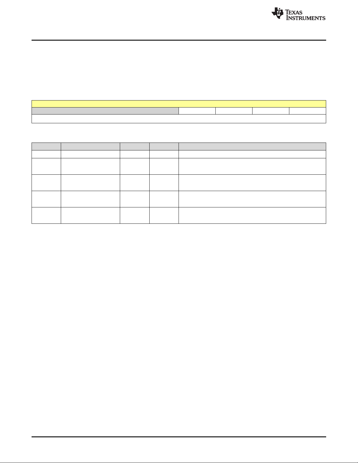
FUNC_RESOURCE Registers
3.8.11 ENABLE2_RES_ASSIGN Register (Address = 1E2h) [reset = 0h]
ENABLE2_RES_ASSIGN is shown in Figure 3-84 and described in Table 3-92.
Return to Summary Table.
ENABLE2 resource assignment register
RESET register domain: HWRST
Figure 3-84. ENABLE2_RES_ASSIGN Register
7 6 5 4 3 2 1 0
RESERVED PLL_EN REGEN3 REGEN2 REGEN1
R-0h R/W-0h R/W-0h R/W-0h R/W-0h
Table 3-92. ENABLE2_RES_ASSIGN Register Field Descriptions
Bit Field Type Reset Description
7-4 RESERVED R 0h
3 PLL_EN R/W 0h
2 REGEN3 R/W 0h
1 REGEN2 R/W 0h
0 REGEN1 R/W 0h
0: ENABLE2 has no effect on PLL_EN
1: PLL_EN is controlled by ENABLE2
0: ENABLE2 has no effect on REGEN3
1: REGEN3 is controlled by ENABLE2
0: ENABLE2 has no effect on REGEN2
1: REGEN2 is controlled by ENABLE2
0: ENABLE2 has no effect on REGEN1
1: REGEN1 is controlled by ENABLE2
www.ti.com
100
Register Descriptions
Copyright © 2015–2017, Texas Instruments Incorporated
SLVUAH1C–June 2015–Revised April 2017
Submit Documentation Feedback
 Loading...