Texas Instruments TPS659101A1RSL, TPS659102A1RSL, TPS659103A1RSL, TPS659104A1RSL, TPS659105A1RSL Schematic [ru]
...
TPS65910, TPS65910A, TPS65910A3, TPS659101, TPS659102, TPS659103
TPS659104, TPS659105, TPS659106, TPS659107, TPS659108, TPS659109
www.ti.com
SWCS046T –MARCH 2010–REVISED SEPTEMBER 2013
Integrated Power Management Unit Top Specification
Check for
Samples: TPS65910, TPS65910A, TPS65910A3, TPS659101, TPS659102, TPS659103, TPS659104, TPS659105, TPS659106,
1
FEATURES
The purpose of the TPS65910 device is to
provide the following resources:
• Embedded power controller
• Two efficient step-down dc-dc converters for
processor cores
• One efficient step-down dc-dc converter for I/O
power
• One efficient step-up 5-V dc-dc converter
• SmartReflex™ compliant dynamic voltage
management for processor cores
• 8 LDO voltage regulators and one RTC LDO
(internal purpose)
• One high-speed I2C interface for generalpurpose control commands (CTL-I2C)
• One high-speed I2C interface for SmartReflex
Class 3 control and command (SR-I2C)
• Two enable signals multiplexed with SR-I2C,
configurable to control any supply state and
processor cores supply voltage
• Thermal shutdown protection and hot-die
detection
• A real-time clock (RTC) resource with:
– Oscillator for 32.768-kHz crystal or 32-kHz
built-in RC oscillator
– Date, time and calendar
– Alarm capability
• One configurable GPIO
• DC-DC switching synchronization through
internal or external 3-MHz clock
TPS659107, TPS659108, TPS659109
APPLICATIONS
• Portable and handheld systems
• OMAP3 power management
DESCRIPTION
The TPS65910 is an integrated power-management
IC available in 48-QFN package and dedicated to
applications powered by one Li-Ion or Li-Ion polymer
battery cell or 3-series Ni-MH cells, or by a 5-V input;
it requires multiple power rails. The device provides
three step-down converters, one step-up converter,
and eight LDOs and is designed to support the
specific power requirements of OMAP-based
applications.
Two of the step-down converters provide power for
dual processor cores and are controllable by a
dedicated class-3 SmartReflex interface for optimum
power savings. The third converter provides power for
the I/Os and memory in the system.
The device includes eight general-purpose LDOs
providing a wide range of voltage and current
capabilities; they are fully controllable by the I2C
interface. The use of the LDOs is flexible; they are
intended to be used as follows: Two LDOs are
designated to power the PLL and video DAC supply
rails on the OMAP based processors, four generalpurpose auxiliary LDOs are available to provide
power to other devices in the system, and two LDOs
are provided to power DDR memory supplies in
applications requiring these memories.
In addition to the power resources, the device
contains an embedded power controller (EPC) to
manage the power sequencing requirements of the
OMAP systems and an (RTC).
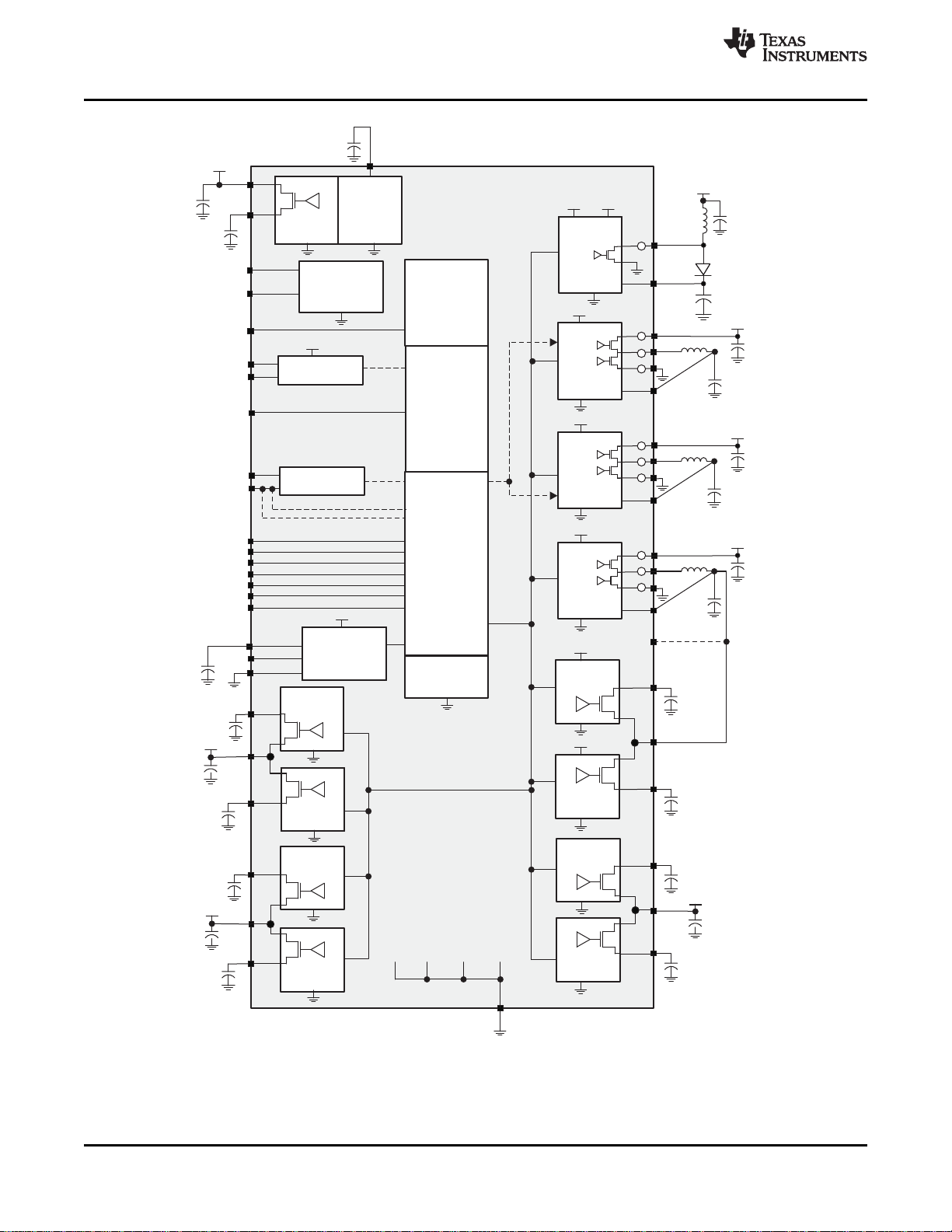
Figure 1 shows the top-level diagram of the device.
1
Please be aware that an important notice concerning availability, standard warranty, and use in critical applications of
Texas Instruments semiconductor products and disclaimers thereto appears at the end of this data sheet.
PRODUCTION DATA information is current as of publication date.
Products conform to specifications per the terms of the Texas
Instruments standard warranty. Production processing does not
necessarily include testing of all parameters.
Copyright © 2010–2013, Texas Instruments Incorporated
VFB1
INT1
PWRON
VREF
REFGND
Test interface
CLK32KOUT
VAUX33
VMMC
OSC32KIN
OSC32KOUT
TESTV
SLEEP
NRESPWRON
PWRHOLD
BOOT1
BOOT0
SDASR_EN2
SCLSR_EN1
SDA_SDI
VDAC
VPLL
VAUX1
VRTC
Real-time
clock
VFB3
SW3
VDIG2
VAUX2
VDIG1
VDD1
(SMPS)
VCC1
GND1
SW1
VFBIO
VBAT
VCC7
VCC7
VCC7
VBAT
VBAT
VBAT
VCC6
VCC3
VCC4
VCC5
VCC 7
VBAT
VCC7
VDDIO
VDDIO
AGND2
AGND
AGND
GNDA
GNDA
DGND
VAUX33
REFGND
GND3
OSC
32-kHz
SCL_SCK
Bus
control
GPIO_CKSYNC
Power
control
state-
machine
Analog
references
and comparators
VBACKUP
Backup
management
VRTC (LDO)
and POR
VFB2
VCC2
GND2
SW2
VCCIO
GNDIO
SWIO
GNDP
AGND
AGND2
AGND2
VDAC
(LDO)
VPLL
(LDO)
VAUX1
(LDO)
VAUX2
(LDO)
VDIG1
(LDO)
AGND2
AGND2
AGND2
VDIG2
(LDO)
VAUX33
(LDO)
VMMC
(LDO)
I C
2
I C
2
AGND2
AGND
AGND
VCC7
VCC7
VCC4
VDD2
(SMPS)
VIO
(SMPS)
VDD3
(SMPS)
SWCS046-001
GNDP: Power pad ground
Ci
(VCC7)
Co
(VRTC)
Co
(VREF)
Co
(VDAC)
Ci
(VCC5)
C
BB
Co
(VPLL)
Co
(VAUX1)
Ci
(VCC4)
Co
(VAUX2)
DGND AGND AGND2
GND3
Co
(VMMC)
VBAT
Ci
(VCC4)
Co
(VAUX33)
Co
(VDIG2)
Co
(VDIG1)
Co
(VIO)
Ci
(VCCIO)
VBAT
Ci
(VCC2)
Co
(VDD2)
VBAT
Ci
(VCC1)
Co
(VDD1)
Co
(VDD3)
Ci
(VDD3)
TPS65910, TPS65910A, TPS65910A3, TPS659101, TPS659102, TPS659103
TPS659104, TPS659105, TPS659106, TPS659107, TPS659108, TPS659109
SWCS046T –MARCH 2010–REVISED SEPTEMBER 2013
2 Submit Documentation Feedback Copyright © 2010–2013, Texas Instruments Incorporated
Product Folder Links: TPS65910 TPS65910A TPS65910A3 TPS659101 TPS659102 TPS659103 TPS659104
Figure 1. 48-QFN Top-Level Diagram
TPS659105 TPS659106 TPS659107 TPS659108 TPS659109
www.ti.com
TPS65910, TPS65910A, TPS65910A3, TPS659101, TPS659102, TPS659103
TPS659104, TPS659105, TPS659106, TPS659107, TPS659108, TPS659109
www.ti.com
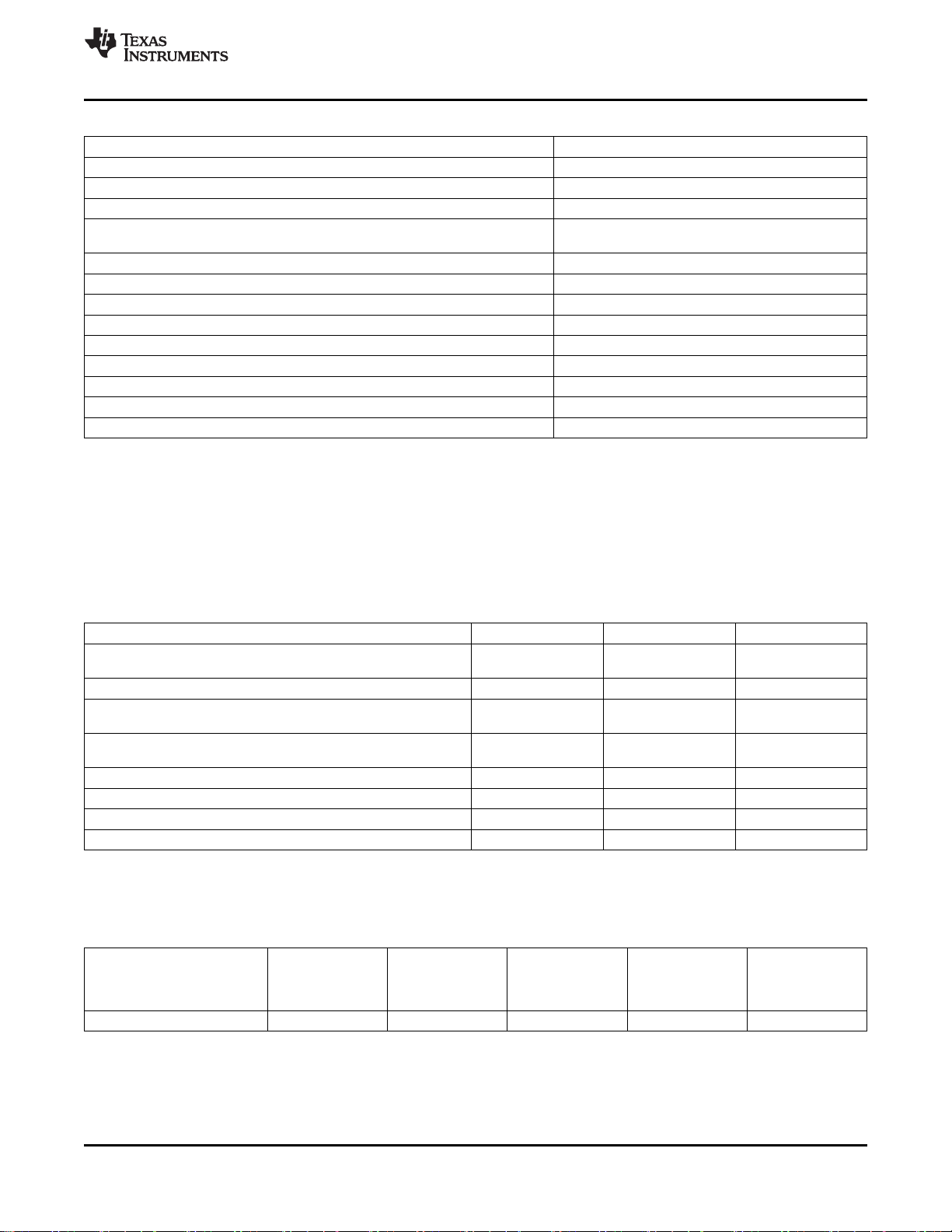
Table 1. SUPPORTED PROCESSORS AND CORRESPONDING PART NUMBERS
Compatible Processor
TI processor - AM335x with DDR2 TPS65910AA1RSL
TI processor - AM335x with DDR3 TPS65910A3A1RSL
TI processor - AM335x with DDR3
TI processors - AM1705/07, AM1806/08, AM3505/17, AM3703/15, DM3730/25, TPS65910A1RSL
OMAP-L137/38, OMAP3503/15/25/30, TMS320C6742/6/8
Samsung - S5PV210, S5PC110 TPS659101A1RSL
Rockchip - RK29xx, RK30xx TPS659102A1RSL
Samsung - S5PC100 TPS659103A1RSL
Samsung - S5P6440 TPS659104A1RSL
TI processors - DM643x, DM644x TPS659105A1RSL
Reserved TPS659106A1RSL
Freescale - i.MX27, Freescale - i.MX35 TPS659107A1RSL
Freescale - i.MX508 TPS659108A1RSL
Freescale - i.MX51 TPS659109A1RSL
(1) The RSL package is available in tape and reel. See for details for corresponding part numbers, quantities and ordering information.
(2) Refer to SWCU093 document.
(1)
(2)
SWCS046T –MARCH 2010–REVISED SEPTEMBER 2013
Part Number
TPS65910A31A1RSL
(1)
ABSOLUTE MAXIMUM RATINGS
over operating free-air temperature range (unless otherwise noted)
Stresses beyond those listed under below may cause permanent damage to the device. These are stress ratings only and
functional operation of the device at these or any other conditions beyond those indicated below are not implied. Exposure to
absolute-maximum-rated conditions for extended periods may affect device reliability.
The absolute maximum ratings for the TPS65910 device are listed below:
PARAMETER MIN MAX UNIT
Voltage range on pins/balls VCC1, VCC2, VCCIO, VCC3, VCC4,
VCC5, VCC6, VCC7
Voltage range on pins/balls VDDIO –0.3 3.6 V
Voltage range on pins/balls OSC32KIN, OSC32KOUT, BOOT1,
BOOT0
Voltage range on pins/balls SDA_SDI, SCL_SCK, SDASR_EN2,
SCLSR_EN1, SLEEP, INT1, CLK32KOUT, NRESPWRON
Voltage range on pins/balls PWRON –0.3 7 V
Voltage range on pins/balls PWRHOLD
Functional junction temperature range –45 150 °C
Peak output current on all other terminals than power resources –5 5 mA
(1) I/O supplied from VDDIO but which can be driven from to a VBAT voltage level
(2) I/O supplied from VRTC but can be driven to a VBAT voltage level
(1)
GPIO_CKSYNC
(2)
–0.3 7 V
–0.3 VRTC
–0.3 VDDIO
–0.3 7 V
+ 0.3 V
MAX
+ 0.3 V
MAX
THERMAL CHARACTERISTICS
over operating free-air temperature range (unless otherwise noted)
Package R
RSL 48-QFN 37 2.6 37 1.48 1
θja
(°C/W)
TA < 25°C Power FACTOR ABOVE TA = 70°C Power TA = 85°C Power
Rating (W) 25 °C (W) Rating (W)
DERATING
(mW/°C)
The thermal resistance R
The value of thermal resistance R
Copyright © 2010–2013, Texas Instruments Incorporated Submit Documentation Feedback 3
Product Folder Links: TPS65910 TPS65910A TPS65910A3 TPS659101 TPS659102 TPS659103 TPS659104
junction-to-power PAD of the RSL package is 1.1°C/W
θJP
junction-to-ambient was measured on a high K.
θJA
TPS659105 TPS659106 TPS659107 TPS659108 TPS659109
TPS65910, TPS65910A, TPS65910A3, TPS659101, TPS659102, TPS659103
TPS659104, TPS659105, TPS659106, TPS659107, TPS659108, TPS659109
SWCS046T –MARCH 2010–REVISED SEPTEMBER 2013
RECOMMENDED OPERATING CONDITIONS
over operating free-air temperature range (unless otherwise noted)
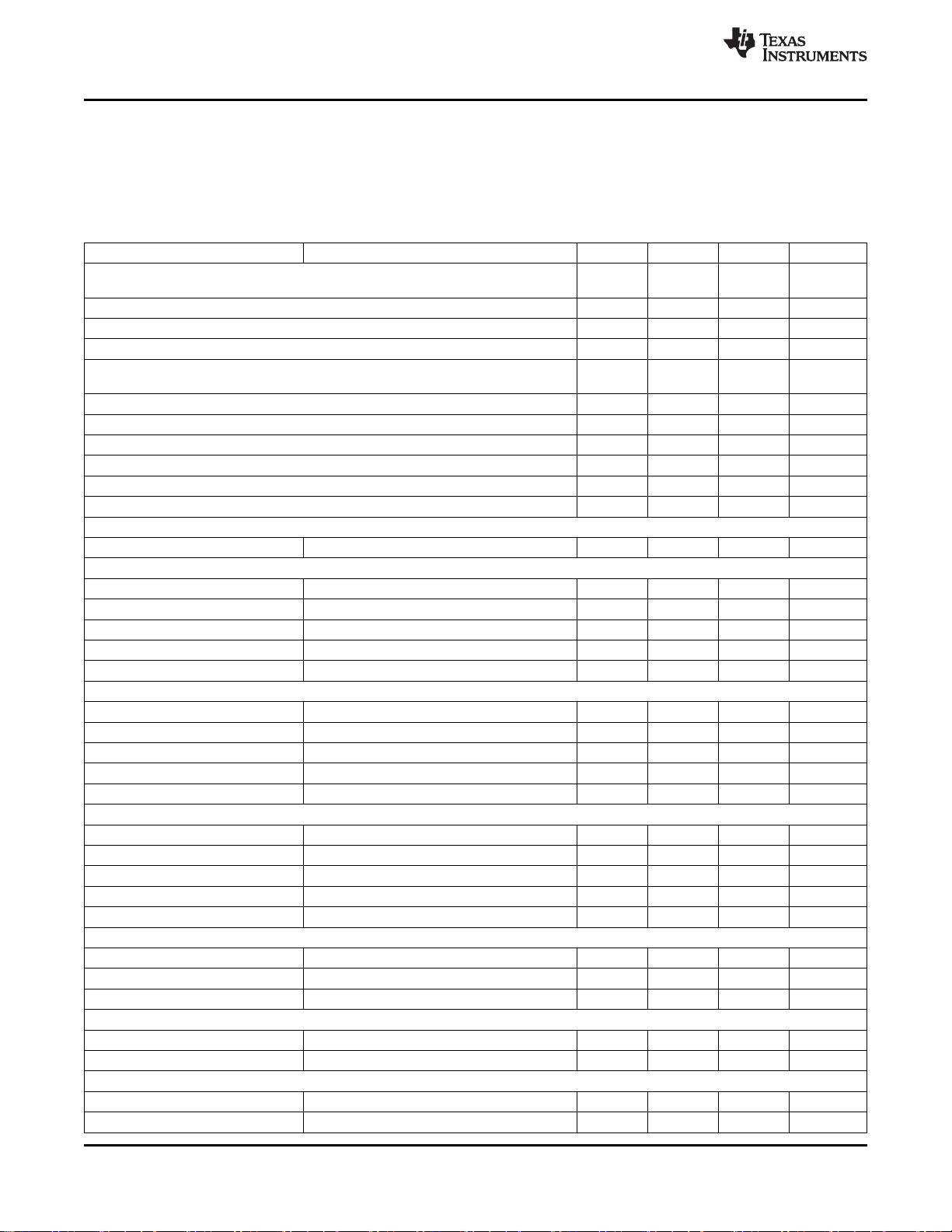
Lists of the recommended operating maximum ratings for the TPS65910 device are given below.
Note1: VCC7 should be connected to the highest supply that is connected to the device VCCx pin. The exception is that
VCC2 and VCC4 can be higher than VCC7.
Note2: VCC2 and VCC4 must be connected together (to the same voltage).
Note3: If VDD3 boost is used, VAUX33 must be set to 2.8 V or higher and enabled before VDD3.
PARAMETER TEST CONDITIONS MIN NOM MAX UNIT
VCC: Input voltage range on pins/balls VCC1, VCC2, VCCIO, VCC3, VCC4, VCC5,
VCC7
V
: Input voltage range on pins/balls VCC6 1.7 3.6 5.5 V
CCP
Input voltage range on pins/balls VDDIO 1.65 1.8/3.3 3.45 V
Input voltage range on pins/balls PWRON 0 3.6 5.5 V
Input voltage range on pins/balls SDA_SDI, SCL_SCK, SDASR_EN2, SCLSR_EN1,
SLEEP
Input voltage range on pins/balls PWRHOLD, GPIO_CKSYNC 1.65 VDDIO 5.5 V
Input voltage range on balls BOOT1, BOOT0, OSC32KIN 1.65 VRTC 1.95 V
Operating free-air temperature, T
Junction temperature T
J
A
Storage temperature range –65 27 150 °C
Lead temperature (soldering, 10 s) 260 °C
Power References
VREF filtering capacitor C
O(VREF)
Connected from VREF to REFGND 100 nF
VDD1 SMPS
Input capacitor C
Filter capacitor C
I(VCC1)
O(VDD1)
X5R or X7R dielectric 10 µF
X5R or X7R dielectric 4 10 12 µF
COfilter capacitor ESR f = 3 MHz 10 300 mΩ
Inductor L
LOinductor dc resistor DCR
O(VDD1)
L
VDD2 SMPS
Input capacitor C
Filter capacitor C
I(VCC2)
O(VDD2)
X5R or X7R dielectric 10 µF
X5R or X7R dielectric 4 10 12 µF
COfilter capacitor ESR f = 3 MHz 10 300 mΩ
Inductor L
LOinductor dc resistor DCR
O(VDD2)
L
VIO SMPS
Input capacitor C
Filter capacitor C
I(VIO)
O(VIO)
X5R or X7R dielectric 10 µF
X5R or X7R dielectric 4 10 12 µF
COfilter capacitor ESR f = 3 MHz 10 300 mΩ
Inductor L
LOinductor dc resistor DCR
O(VIO)
L
VDIG1 LDO
Input capacitor C
I(VCC6)
Filtering capacitor C
O(VDIG1)
X5R or X7R dielectric 4.7 µF
COfiltering capacitor ESR 0 500 mΩ
VDIG2 LDO
Filtering capacitor C
O(VDIG2)
COfiltering capacitor ESR 0 500 mΩ
VPLL LDO
Input capacitor C
I(VCC5)
Filtering capacitor C
O(VPLL)
X5R or X7R dielectric 4.7 µF
2.7 3.6 5.5 V
1.65 VDDIO 3.45 V
–40 27 85 °C
–40 27 125 °C
2.2 µH
125 mΩ
2.2 µH
125 mΩ
2.2 µH
125 mΩ
0.8 2.2 2.64 µF
0.8 2.2 2.64 µF
0.8 2.2 2.64 µF
www.ti.com
4 Submit Documentation Feedback Copyright © 2010–2013, Texas Instruments Incorporated
Product Folder Links: TPS65910 TPS65910A TPS65910A3 TPS659101 TPS659102 TPS659103 TPS659104
TPS659105 TPS659106 TPS659107 TPS659108 TPS659109
TPS65910, TPS65910A, TPS65910A3, TPS659101, TPS659102, TPS659103
TPS659104, TPS659105, TPS659106, TPS659107, TPS659108, TPS659109
www.ti.com
RECOMMENDED OPERATING CONDITIONS (continued)
over operating free-air temperature range (unless otherwise noted)
Lists of the recommended operating maximum ratings for the TPS65910 device are given below.
Note1: VCC7 should be connected to the highest supply that is connected to the device VCCx pin. The exception is that
VCC2 and VCC4 can be higher than VCC7.
Note2: VCC2 and VCC4 must be connected together (to the same voltage).
Note3: If VDD3 boost is used, VAUX33 must be set to 2.8 V or higher and enabled before VDD3.
PARAMETER TEST CONDITIONS MIN NOM MAX UNIT
COfiltering capacitor ESR 0 500 mΩ
VDAC LDO
Filtering capacitor C
COfiltering capacitor ESR 0 500 mΩ
Input capacitor C
Filtering capacitor C
COfiltering capacitor ESR 0 500 mΩ
Filtering capacitor C
COfiltering capacitor ESR 0 500 mΩ
Input capacitor C
Filtering capacitor C
COfiltering capacitor ESR 0 500 mΩ
Filtering capacitor C
COfiltering capacitor ESR 0 500 mΩ
Input capacitor C
Filtering capacitor C
COfiltering capacitor ESR 0 500 mΩ
Input capacitor C
Filter capacitor C
COfilter capacitor ESR f = 1 MHz 10 300 mΩ
Inductor L
O(VDD3)
LOinductor DC resistor DCR
Backup battery capacitor C
Series resistors Ω
SDA_SDI, SCL_SCK, SDASR_EN2,
SCLSR_EN1 external pull-up resistor
Crystal frequency @ specified load cap value 32.768 kHz
Crystal tolerance @ 27°C –20 0 20 ppm
Frequency Temperature coefficient. –0.5 0.5 ppm/°C
Secondary temperature coefficient –0.04 –0.035 –0.03 ppm/°C
Voltage coefficient –2 2 ppm/V
O(VDAC)
I(VCC4)
O(VMMC)
O(VAUX33)
I(VCC3)
O(VAUX1)
O(VAUX2)
I(VCC7)
O(VRTC)
I(VDD3)
O(VDD3)
VMMC LDO
X5R or X7R dielectric 4.7 µF
VAUX33 LDO
VAUX1 LDO
X5R or X7R dielectric 4.7 µF
VAUX2 LDO
VRTC LDO
X5R or X7R dielectric 4.7 µF
VDD3 SMPS
X5R or X7R dielectric 4.7 µF
X5R or X7R dielectric 4 10 12 µF
L
Backup Battery
Battery or superCap supplying VBACKUP 5 10 2000 mF
BB
Capacitor supplying VBACKUP 1 40 µF
5 to 15 mF 10 1500
100 to 2000 mF 5 15
I2C Interfaces
Connected to VDDIO 1.2 kΩ
Crystal Oscillator (connected from OSC32KIN to OSC32KOUT)
Oscillator contribution (not including crystal
variation)
SWCS046T –MARCH 2010–REVISED SEPTEMBER 2013
0.8 2.2 2.64 µF
0.8 2.2 2.64 µF
0.8 2.2 2.64 µF
0.8 2.2 2.64 µF
0.8 2.2 2.64 µF
0.8 2.2 2.64 µF
2.8 4.7 6.6 µH
50 500 mΩ
2
Copyright © 2010–2013, Texas Instruments Incorporated Submit Documentation Feedback 5
Product Folder Links: TPS65910 TPS65910A TPS65910A3 TPS659101 TPS659102 TPS659103 TPS659104
TPS659105 TPS659106 TPS659107 TPS659108 TPS659109
TPS65910, TPS65910A, TPS65910A3, TPS659101, TPS659102, TPS659103
TPS659104, TPS659105, TPS659106, TPS659107, TPS659108, TPS659109
SWCS046T –MARCH 2010–REVISED SEPTEMBER 2013
RECOMMENDED OPERATING CONDITIONS (continued)
over operating free-air temperature range (unless otherwise noted)
Lists of the recommended operating maximum ratings for the TPS65910 device are given below.
Note1: VCC7 should be connected to the highest supply that is connected to the device VCCx pin. The exception is that
VCC2 and VCC4 can be higher than VCC7.
Note2: VCC2 and VCC4 must be connected together (to the same voltage).
Note3: If VDD3 boost is used, VAUX33 must be set to 2.8 V or higher and enabled before VDD3.
PARAMETER TEST CONDITIONS MIN NOM MAX UNIT
Max crystal series resistor @ Fundamental frequency 90 kΩ
Crystal load capacitor According to crystal data sheet 6 12.5 pF
Load crystal oscillator Coscin
,Coscout
Quality factor 8000 80000
parallel mode Including parasitic PCB capacitor 12 25 pF
ESD SPECIFICATIONS
over operating free-air temperature range (unless otherwise noted)
ESD METHOD STANDARD REFERENCE PERFORMANCE
Human body model (HBM) EIA/JESD22-A114D 2000 V 2000 V
Charge device model (CDM) EIA/JESD22-C101C 500 V 500 V
TI STANDARD
REQUIREMENTS
www.ti.com
6 Submit Documentation Feedback Copyright © 2010–2013, Texas Instruments Incorporated
Product Folder Links: TPS65910 TPS65910A TPS65910A3 TPS659101 TPS659102 TPS659103 TPS659104
TPS659105 TPS659106 TPS659107 TPS659108 TPS659109
TPS65910, TPS65910A, TPS65910A3, TPS659101, TPS659102, TPS659103
TPS659104, TPS659105, TPS659106, TPS659107, TPS659108, TPS659109
www.ti.com
I/O PULLUP AND PULLDOWN CHARACTERISTICS
over operating free-air temperature range (unless otherwise noted)
PARAMETER TEST CONDITIONS MIN TYP MAX UNIT
SDA_SDI, SCL_SCK, SDASR_EN2,
SCLSR_EN1 Programmable pullup (DFT, default Grounded, VDDIO = 1.8 V –45% 8 +45% kΩ
inactive)
SLEEP programmable pulldown (default active) @ 1.8 V, VRTC = 1.8 V 2 4.5 10 µA
@ 1.8 V, VRTC = 1.8 V, VCC7 = 2.7
PWRHOLD programmable pulldown (default
active)
BOOT0, BOOT1 programmable pulldown (default
active)
NRESPWRON pulldown @ 1.8 V, VCC7 = 5.5 V, OFF state 2 4.5 10 µA
32KCLKOUT pulldown (disabled in Active-sleep
state)
PWRON programmable pullup (default active) Grounded, VCC7 = 5.5 V –40 –31 –15 µA
GPIO_CKSYNC programmable pullup (default
active)
(1) The internal pullups on the CTL-I2C and SR-I2C balls are used for test purposes or when the SR-I2C interface is not used. Discrete
pullups to the VIO supply must be mounted on the board in order to use the I2C interfaces. The internal I2C pullups must not be used for
functional applications
V
@ 5.5 V, VRTC = 1.8 V, VCC7 = 5.5
V
@ 1.8 V, VRTC = 1.8 V 2 4.5 10 µA
@ 1.8 V, VRTC = 1.8 V, OFF state 2 4.5 10 µA
Grounded, VRTC = 1.8 V –27 –18 –9 µA
(1)
SWCS046T –MARCH 2010–REVISED SEPTEMBER 2013
2 4.5 10
7 14 30
µA
Copyright © 2010–2013, Texas Instruments Incorporated Submit Documentation Feedback 7
Product Folder Links: TPS65910 TPS65910A TPS65910A3 TPS659101 TPS659102 TPS659103 TPS659104
TPS659105 TPS659106 TPS659107 TPS659108 TPS659109
TPS65910, TPS65910A, TPS65910A3, TPS659101, TPS659102, TPS659103
TPS659104, TPS659105, TPS659106, TPS659107, TPS659108, TPS659109
SWCS046T –MARCH 2010–REVISED SEPTEMBER 2013
DIGITAL I/O VOLTAGE ELECTRICAL CHARACTERISTICS
over operating free-air temperature range (unless otherwise noted)
PARAMETER MIN TYP MAX UNIT
Related I/O: PWRON
Low-level input voltage V
High-level input voltage V
IL
IH
0.7 x VCC7 V
Related I/Os: PWRHOLD, GPIO_CKSYNC
Low-level input voltage V
High-level input voltage V
IL
IH
1.3 VCC7 V
VDDIO/V
CC7
Related I/Os: BOOT0, BOOT1, OSC32KIN
Low-level input voltage V
High-level input voltage V
IL
IH
0.65 x VRTC V
Related I/Os: SLEEP
Low-level input voltage V
High-level input voltage V
IL
IH
0.65 x VDDIO V
Related I/Os: NRESPWRON, INT1, 32KCLKOUT
Low-level output voltage V
OL
IOL= 100 µA 0.2 V
IOL= 2 mA 0.45 V
High-level output voltage V
OH
IOH= 100 µA VDDIO – 0.2 V
IOH= 2 mA VDDIO – 0.45 V
Related Open-Drain I/Os: GPIO0
Low-level output voltage V
OL
IOL= 100 µA 0.2 V
IOL= 2 mA 0.45 V
I2C-Specific Related I/Os: SCL, SDA, SCLSR_EN1, SDASR_EN2
Low-level input voltage V
High-level input voltage V
IL
IH
–0.5 0.3 x VDDIO V
0.7 x VDDIO V
Hysteresis 0.1 x VDDIO V
Low-level output voltage VOL@ 3mA (sink current), VDDIO = 1.8 V 0.2 × VDDIO V
Low-level output voltage VOL@ 3mA (sink current), VDDIO = 3.3 V 0.4 x VDDIO V
0.3 x VCC7 V
0.45 V
0.35 x VRTC V
0.35 x VDDIO V
www.ti.com
8 Submit Documentation Feedback Copyright © 2010–2013, Texas Instruments Incorporated
Product Folder Links: TPS65910 TPS65910A TPS65910A3 TPS659101 TPS659102 TPS659103 TPS659104
TPS659105 TPS659106 TPS659107 TPS659108 TPS659109
TPS65910, TPS65910A, TPS65910A3, TPS659101, TPS659102, TPS659103
TPS659104, TPS659105, TPS659106, TPS659107, TPS659108, TPS659109
www.ti.com
I2C INTERFACE AND CONTROL SIGNALS
over operating free-air temperature range (unless otherwise noted)
NO. PARAMETER TEST CONDITIONS MIN TYP MAX
INT1 rise and fall times, CL= 5 to 35 pF 5 10 ns
NRESPWRON rise and fall times, CL= 5 to 35 pF 5 10 ns
SLAVE HIGH–SPEED MODE
SCL/SCLSR_EN1 and SDA/SDASR_EN2 rise and fall
time, CL= 10 to 100 pF
Data rate 3.4 Mbps
I3 t
I4 t
I7 t
I8 t
I9 t
I3 t
I4 t
I7 t
I8 t
I9 t
I3 t
I4 t
I7 t
I8 t
I9 t
I1 t
I2 t
I1 t
I2 t
I1 t
I2 t
su(SDA-SCLH)
h(SCLL-SDA)
su(SCLH-SDAL)
h(SDAL-SCLL)
su(SDAH-SCLH)
su(SDA-SCLH)
h(SCLL-SDA)
su(SCLH-SDAL)
h(SDAL-SCLL)
su(SDAH-SCLH)
su(SDA-SCLH)
h(SCLL-SDA)
su(SCLH-SDAL)
h(SDAL-SCLL)
su(SDAH-SCLH)
w(SCLL)
w(SCLH)
w(SCLL)
w(SCLH)
w(SCLL)
w(SCLH)
Setup time, SDA valid to SCL high 10 ns
Hold time, SDA valid from SCL low 0 70 ns
Setup time, SCL high to SDA low 160 ns
Hold time, SCL low from SDA low 160 ns
Setup time, SDA high to SCL high 160 ns
SLAVE FAST MODE
SCL/SCLSR_EN1 and SDA/SDASR_EN2 rise and fall 20 +
time, CL= 10 to 400 pF 0.1 × C
Data rate 400 Kbps
Setup time, SDA valid to SCL high 100 ns
Hold time, SDA valid from SCL low 0 0.9 µs
Setup time, SCL high to SDA low 0.6 µs
Hold time, SCL low from SDA low 0.6 µs
Setup time, SDA high to SCL high 0.6 µs
SLAVE STANDARD MODE
SCL/SCLSR_EN1 and SDA/SDASR_EN2 rise and fall
time, CL= 10 to 400 pF
Data rate 100 Kbps
Setup time, SDA valid to SCL high 250 ns
Hold time, SDA valid from SCL low 0 µs
Setup time, SCL high to SDA low 4.7 µs
Hold time, SCL low from SDA low 4 µs
Setup time, SDA high to SCL high 4 µs
SWITCHING CHARACTERISTICS
SLAVE HIGH–SPEED MODE
Pulse duration, SCL low 160 ns
Pulse duration, SCL high 60 ns
SLAVE FAST MODE
Pulse duration, SCL low 1.3 µs
Pulse duration, SCL high 0.6 µs
SLAVE STANDARD MODE
Pulse duration, SCL low 4.7 µs
Pulse duration, SCL high 4 µs
SWCS046T –MARCH 2010–REVISED SEPTEMBER 2013
10 80 ns
L
250 ns
250 ns
Copyright © 2010–2013, Texas Instruments Incorporated Submit Documentation Feedback 9
Product Folder Links: TPS65910 TPS65910A TPS65910A3 TPS659101 TPS659102 TPS659103 TPS659104
TPS659105 TPS659106 TPS659107 TPS659108 TPS659109

TPS65910, TPS65910A, TPS65910A3, TPS659101, TPS659102, TPS659103
TPS659104, TPS659105, TPS659106, TPS659107, TPS659108, TPS659109
SWCS046T –MARCH 2010–REVISED SEPTEMBER 2013
POWER CONSUMPTION
over operating free-air temperature range (unless otherwise noted)
All current consumption measurements are relative to the FULL chip, all VCC inputs set to VBAT voltage.
PARAMETER TEST CONDITIONS MIN TYP MAX UNIT
Device BACKUP state VBAT = 2.4 V, VBACKUP = 0 V, 11 16
VBAT = 0 V, VBACKUP = 3.2 V 6 9
Device OFF state VBAT = 3.6 V, CK32K clock running
BOOT[1:0] = 00: 32-kHz RC oscillator 16.5 23
BOOT[1:0] = 01: 32-kHz quartz or bypass oscillator, BOOT0P
= 0
BOOT[1:0] = 01, Backup Battery Charger on, VBACKUP = 3.2
V
VBAT = 5 V, CK32K clock running: 20 28
BOOT[1:0] = 00: RC oscillator
Device SLEEP state VBAT = 3.6 V, CK32K clock running, PWRHOLDP = 0
BOOT[1:0] = 00, 3 DC-DCs on, 5 LDOs and VRTC on, no load 295
BOOT[1:0] = 01, 3 DC-DCs on, 3 LDOs and VRTC on, no load,
BOOT0P = 0
Device ACTIVE state VBAT = 3.6 V, CK32K clock running, PWRHOLDP = 0
BOOT[1:0] = 00, 3 DC-DCs on, 5 LDOs and VRTC on, no load 1
BOOT[1:0] = 01, 3 DC-DCs on, 3 LDOs and VRTC on, no load,
BOOT0P = 0
BOOT[1:0] = 00, 3 DC-DCs on PWM mode (VDD1_PSKIP =
VDD2_PSKIP = VIO_PSKIP = 0), 5 LDOs and VRTC on, no 21
load
15 20
32 42
279
0.9
www.ti.com
µA
µA
µA
mA
POWER REFERENCES AND THRESHOLDS
over operating free-air temperature range (unless otherwise noted)
PARAMETER TEST CONDITIONS MIN TYP MAX UNIT
Output reference voltage (VREF
terminal)
Main battery charged Measured on VCC7 terminal
threshold VMBCH (programmable) Triggering monitored through NRESPRWON
Main battery discharged Measured on VCC7 terminal (MTL prg) VMBCH –
threshold VMBDCH (programmable) Triggering monitored through INT1 100 mV
Main battery low threshold VMBLO Measured on VCC7 terminal (Triggering
(MB comparator) monitored on terminal NRESPWRON)
Main battery high threshold VMBHI 2.6 2.75 3
Main battery not present threshold Measured on terminal VCC7
VBNPR (Triggering monitored on terminal VRTC)
Ground current (analog references
+ comparators + backup battery Device in OFF state 8
switch)
Device in active or low-power mode –1% 0.85 +1% V
VMBCH_VSEL = 11, BOOT[1:0] = 11 or 00 3
VMBCH_VSEL = 10 2.9
VMBCH_VSEL = 01 2.8
VMBCH_VSEL = 00 bypassed
2.5 2.6 2.7 V
VBACKUP = 0 V, measured on terminal VCC7
(MB comparator)
VBACKUP = 3.2 V, measured on terminal VCC7 2.5 2.55 3
1.9 2.1 2.2 V
VCC= 3.6 V
Device in ACTIVE or SLEEP state 20
V
V
V
µA
10 Submit Documentation Feedback Copyright © 2010–2013, Texas Instruments Incorporated
Product Folder Links: TPS65910 TPS65910A TPS65910A3 TPS659101 TPS659102 TPS659103 TPS659104
TPS659105 TPS659106 TPS659107 TPS659108 TPS659109
TPS65910, TPS65910A, TPS65910A3, TPS659101, TPS659102, TPS659103
TPS659104, TPS659105, TPS659106, TPS659107, TPS659108, TPS659109
www.ti.com
THERMAL MONITORING AND SHUTDOWN
over operating free-air temperature range (unless otherwise noted)
PARAMETER TEST CONDITIONS MIN TYP MAX UNIT
Hot-die temperature rising threshold THERM_HDSEL[1:0] = 00 117
THERM_HDSEL[1:0] = 01 121
THERM_HDSEL[1:0] = 10 113 125 136
THERM_HDSEL[1:0] = 11 130
Hot-die temperature hysteresis 10 °C
Thermal shutdown temperature rising
threshold
Thermal shutdown temperature hysteresis 10 °C
Ground current 6 µA
Device in ACTIVE state, Temp = 27°C,
VCC7 = 3.6 V
32-kHz RTC CLOCK
over operating free-air temperature range (unless otherwise noted)
PARAMETER TEST CONDITIONS MIN TYP MAX UNIT
CLK32KOUT rise and fall time CL= 35 pF 10 ns
Bypass Clock (OSC32KIN: input, OSC32KOUT floating)
Input bypass clock frequency OSCKIN input 32 kHz
Input bypass clock duty cycle OSCKIN input 40% 60%
Input bypass clock rise and fall time 10% – 90%, OSC32KIN input, 10 20 ns
CLK32KOUT duty cycle Logic output signal 40% 60%
Bypass clock setup time 32KCLKOUT output 1 ms
Ground current Bypass mode 1.5 µA
Crystal oscillator (connected from OSC32KIN to OSC32KOUT)
Output frequency CK32KOUT output 32.768 kHz
Oscillator startup time On power on 2 s
Ground current 1.5 µA
RC oscillator (OSC32KIN: grounded, OSC32KOUT floating)
Output frequency CK32KOUT output 32 kHz
Output frequency accuracy @ 25°C –15% 0% +15%
Cycle jitter (RMS) Oscillator contribution +10%
Output duty cycle +40% +50% +60%
Settling time 150 µs
Ground current Active @ fundamental frequency 4 µA
SWCS046T –MARCH 2010–REVISED SEPTEMBER 2013
136 148 160 °C
°C
Copyright © 2010–2013, Texas Instruments Incorporated Submit Documentation Feedback 11
Product Folder Links: TPS65910 TPS65910A TPS65910A3 TPS659101 TPS659102 TPS659103 TPS659104
TPS659105 TPS659106 TPS659107 TPS659108 TPS659109

TPS65910, TPS65910A, TPS65910A3, TPS659101, TPS659102, TPS659103
TPS659104, TPS659105, TPS659106, TPS659107, TPS659108, TPS659109
SWCS046T –MARCH 2010–REVISED SEPTEMBER 2013
BACKUP BATTERY CHARGER
over operating free-air temperature range (unless otherwise noted)
PARAMETER TEST CONDITIONS MIN TYP MAX UNIT
Backup battery charging current VBACKUP = 0 to 2.4 V, BBCHEN = 1 350 500 700 µA
End-of-charge backup battery
(1)
voltage
Ground current On mode 10 µA
(1) Note:
(a) BBSEL = 10, 00, or 01 intended to charge battery or superCap
(b) BBSEL = 11 intended to charge capacitor
VCC7 = 3.6 V, BBSEL = 10 –3% 3.15 +3%
VCC7 = 3.6 V, BBSEL = 00 –3% 3 +3%
VCC7 = 3.6 V, BBSEL = 01 –3% 2.52 +3%
VCC7 = 3.6 V, BBSEL = 11 VBAT
VBAT –
0.3 V
VRTC LDO
over operating free-air temperature range (unless otherwise noted)
PARAMETER TEST CONDITIONS MIN TYP MAX UNIT
Input voltage V
DC output voltage V
Rated output current I
IN
OUT
OUTmax
DC load regulation On mode, I
DC line regulation On mode, VIN= 3.0 V to V
Transient load regulation On mode, VIN= V
Transient line regulation On mode, VIN= V
Turn-on time 2.2 ms
Ripple rejection
Ground current Device in ACTIVE state 23
(1) These parameters are not tested. They are used for design specification only.
On mode 2.5 5.5
Back-up mode 1.9 5.5
On mode, 3.0 V < VIN< 5.5 V 1.78 1.83 1.88
Back-up mode, 2.3 V ≤ VIN≤ 2.6 V 1.72 1.78 1.84
On mode 20
Back-up mode 0.1
= I
OUT
Back-up mode, I
OUT
Back-up mode, VIN= 2.3 V to 5.5 V @ I
I
OUTmax
I
= I
OUT
and I
OUT
And VIN= V
I
OUTmax
I
= 0, VINrising from 0 up to 3.6 V, @ V
OUT
0.1 V up to V
VIN= V
0.1 V to V
/2 to I
OUTmax
= I
OUTmax
INmin
/2
OUTmin
+ 100 mVpptone, V
INDC
@ I
INmax
to 0 50
OUTmax
INmin
INmin
to V
= I
OUTmax
to I
INmin
OUT
to 0 50
OUTmax
@ I
INmax
+ 0.2 V to V
OUT
INmax
= I
OUT
OUTmax
=
in 5 µs
/2 in 5 µs
OUTmax
+ 0.5 V to V
+ 0.5 V in 30 µs, I
INDC+
= I
OUTmax
in 30 µs 25
INmin
=
OUT
=
OUT
= V
/2
INmin
+
2.5
25
50
f = 217 Hz 55
f = 50 kHz 35
Device in BACKUP or OFF state 3
www.ti.com
(1)
(1)
V
V
V
mA
mV
mV
mV
mV
dB
µA
12 Submit Documentation Feedback Copyright © 2010–2013, Texas Instruments Incorporated
Product Folder Links: TPS65910 TPS65910A TPS65910A3 TPS659101 TPS659102 TPS659103 TPS659104
TPS659105 TPS659106 TPS659107 TPS659108 TPS659109

TPS65910, TPS65910A, TPS65910A3, TPS659101, TPS659102, TPS659103
TPS659104, TPS659105, TPS659106, TPS659107, TPS659108, TPS659109
www.ti.com
VIO SMPS
over operating free-air temperature range (unless otherwise noted)
PARAMETER TEST CONDITIONS MIN TYP MAX UNIT
Input voltage (VCCIO and VCC7) VINI
DC output voltage (V
Rated output current I
)
OUT
OUTmax
P-channel MOSFET VIN= V
On-resistance R
P-channel leakage current I
DS(ON)_PMOS
LK_PMOS
N-channel MOSFET VIN= V
On-resistance R
N-channel leakage current I
DS(ON)_NMOS
LK_NMOS
PMOS current limit (high-side) VIN= V
NMOS current limit (low-side) Source current load:
DC load regulation On mode, I
DC line regulation On mode, VIN= V
Transient load regulation I
t on, off to on I
Overshoot SMPS turned on 3%
Power-save mode Ripple voltage Pulse skipping mode, I
Switching frequency 3 MHz
Duty cycle 100 %
Minimum On Time T
ON(MIN)
P-channel MOSFET
VFBIO internal resistance 0.5 1 MΩ
Discharge resistor for power-down
sequence R
DIS
≤ 800 mA 2.7 5.5
OUT
V
= 1.5 V or 1.8 V, I
OUT
V
= 2.5 V, I
OUT
V
= 3.3 V, I
OUT
> 800 mA 4.0 5.5
OUT
> 800 mA 4.4 5.5
OUT
> 800 mA 3.2 5.5
OUT
PWM mode (VIO_PSKIP = 0) or pulse skip
mode I
OUT
to I
MAX
VSEL=00 –3% 1.5 +3%
VSEL = 01, default BOOT[1:0] = 00 and 01 –3% 1.8 +3%
VSEL = 10 –3% 2.5 +3% V
VSEL = 11 –3% 3.3 +3%
Power down 0
ILMAX[1:0] = 00, default 500
ILMAX[1:0] = 01 1000
INmin
VIN= 3.8 V 250 400
VIN= V
, SWIO = 0 V 2 µA
INMAX
MIN
VIN= 3.8 V 250 400
VIN= V
VIN= V
VIN= V
VIN= V
VIN= V
VIN= V
INmax
INmin
INmin
INmin
INmin
INmin
INmin
, SWIO = V
to V
to V
to V
to V
to V
to V
, ILMAX[1:0] = 00 650
INmax
, ILMAX[1:0] = 01 1200 mA
INmax
, ILMAX[1:0] = 10 1700
INmax
, ILMAX[1:0] = 00 650
INmax
, ILMAX[1:0] = 01 1200
INmax
, ILMAX[1:0] = 10 1700
INmax
INmax
Sink current load:
VIN= V
VIN= V
VIN= V
VIN= 3.8 V, V
OUT
I
OUT
OUT
INmin
INmin
INmin
to V
to V
to V
OUT
, ILMAX[1:0] = 00 800
INmax
, ILMAX[1:0] = 01 1200
INmax
, ILMAX[1:0] = 10 1700
INmax
= 0 to I
OUTmax
to V
OUT
INmin
= 1.8 V
INmax
= 0 to 500 mA , Max slew = 100 mA/µs
= 700 to 1200 mA , Max slew = 100 mA/µs
= 200 mA 350 µs
= 1 mA V
OUT
During device switch-off sequence 30 50 Ω
Note: No discharge resistor is applied if VIO is
turned off while the device is on.
SWCS046T –MARCH 2010–REVISED SEPTEMBER 2013
mA
300
300
mΩ
mΩ
2 µA
mA
20 mV
20 mV
50 mV
0.025 ×
V
OUT
35 ns
V
PP
Copyright © 2010–2013, Texas Instruments Incorporated Submit Documentation Feedback 13
Product Folder Links: TPS65910 TPS65910A TPS65910A3 TPS659101 TPS659102 TPS659103 TPS659104
TPS659105 TPS659106 TPS659107 TPS659108 TPS659109

TPS65910, TPS65910A, TPS65910A3, TPS659101, TPS659102, TPS659103
TPS659104, TPS659105, TPS659106, TPS659107, TPS659108, TPS659109
SWCS046T –MARCH 2010–REVISED SEPTEMBER 2013
VIO SMPS (continued)
over operating free-air temperature range (unless otherwise noted)
PARAMETER TEST CONDITIONS MIN TYP MAX UNIT
Ground current (IQ) Off 1
Conversion efficiency
PWM mode, I
VIO_PSKIP = 0
Pulse skipping mode, no switching, 3-MHz clock µA
on
Low-power (pulse skipping) mode, no switching
ST[1:0]=11 63
PWM mode, DCRL< 50 mΩ, V
= 3.6 V:
I
= 10 mA 44%
OUT
I
= 100 mA 87%
OUT
I
= 400 mA 86%
OUT
I
= 800 mA 76%
OUT
I
= 1000 mA 72%
OUT
Pulse Skipping mode, DCRL< 50 mΩ, V
1.8 V, VIN= 3.6 V:
I
= 1 mA 71%
OUT
I
= 10 mA 80%
OUT
I
= 200 mA 87%
OUT
= 0 mA, VIN= 3.8 V,
OUT
OUT
= 1.8 V, V
OUT
7500
250
IN
=
www.ti.com
14 Submit Documentation Feedback Copyright © 2010–2013, Texas Instruments Incorporated
Product Folder Links: TPS65910 TPS65910A TPS65910A3 TPS659101 TPS659102 TPS659103 TPS659104
TPS659105 TPS659106 TPS659107 TPS659108 TPS659109

TPS65910, TPS65910A, TPS65910A3, TPS659101, TPS659102, TPS659103
TPS659104, TPS659105, TPS659106, TPS659107, TPS659108, TPS659109
www.ti.com
VDD1 SMPS
over operating free-air temperature range (unless otherwise noted)
PARAMETER TEST CONDITIONS MIN TYP MAX UNIT
Input voltage (VCC1 and VCC7) VINI
DC output voltage (V
) VGAIN_SEL = 00, I
OUT
DC output voltage programmable
step (V
Rated output current I
OUTSTEP
)
OUTmax
P-channel MOSFET VIN= V
On-resistance R
DS(ON)_PMOS
P-channel leakage current VIN= V
I
LK_PMOS
N-channel MOSFET VIN= V
On-resistance R
N-channel leakage current I
DS(ON)_NMOS
LK_NMOSVIN
PMOS current limit (high-side) VIN= V
NMOS current limit (low-side) Source current load:
DC load regulation On mode, I
DC line regulation On mode, VIN= V
Transient load regulation VIN= 3.8 V, V
t on, off to on I
Output voltage transition rate
Overshoot SMPS turned on 3%
Power-save mode ripple voltage Pulse skipping mode, I
Switching frequency 3 MHz
≤ 1200 mA 2.7 5.5
OUT
V
= 0.6 V to 1.5 V, VGAIN_SEL = 00, V
OUT
I
> 1200 mA V V
OUT
2.5 V ≤ V
I
> 1200 mA
OUT
≤ 3.3 V, VGAIN_SEL = 10 or 11,
OUT
= 0 to I
OUT
OUTmax
:
max programmable voltage, SEL[6:0] = 1001011 1.5
default voltage, BOOT[1:0] = 00 –3% 1.2 +3%
default voltage, BOOT[1:0] = 01 –3% 1.2 +3% V
min programmable voltage, SEL[6:0] = 0000011 0.6
SEL[6:0] = 000000: power down 0
VGAIN_SEL = 10, SEL = 0101011 = 43, I
to I
OUTmax
VGAIN_SEL = 11, SEL = 0101000 = 40, I
to I
OUTmax
VGAIN_SEL = 00, 72 steps 12.5 mV
ILMAX = 0, default 1000 mA
ILMAX = 1 1500
INmin
VIN= 3.8 V 250 400
, SW1 = 0 V 2 µA
INmax
MIN
VIN= 3.8 V 250 400
= V
, SW1 = V
VIN= V
VIN= V
VIN= V
INmax
INmin
INmin
INmin
INmin
to V
to V
to V
to V
INmax
, ILMAX = 0 1150
INmax
, ILMAX = 1 2000
INmax
, ILMAX = 0 1150
INmax
, ILMAX = 1 2000
INmax
Sink current load:
VIN= V
VIN= V
I
OUT
I
OUT
OUT
From V
0.6 V I
INmin
INmin
to V
to V
OUT
, ILMAX = 0 1200
INmax
, ILMAX = 1 2000
INmax
= 0 to I
OUTmax
to V
OUT
INmin
= 1.2 V
INmax
= 0 to 500 mA , Max slew = 100 mA/µs 50 mV
= 700 mA to 1.2A , Max slew = 100 mA/µs
= 200 mA 350 µs
= 0.6 V to 1.5 V and V
OUT
= 500 mA
OUT
OUT
= 1.5 V to
TSTEP[2:0] = 001 12.5
TSTEP[2:0] = 011 (default) 7.5 mV/µs
TSTEP[2:0] = 111 2.5
= 1 mA V
OUT
SWCS046T –MARCH 2010–REVISED SEPTEMBER 2013
+ 2
OUT
5.5
4.5 5.5
= 0
OUT
OUT
–3% 2.2 +3% V
= 0
–3% 3.2 +3% V
300
300
2 µA
20 mV
20 mV
0.025 ×
V
OUT
mΩ
mΩ
mA
mA
PP
Copyright © 2010–2013, Texas Instruments Incorporated Submit Documentation Feedback 15
Product Folder Links: TPS65910 TPS65910A TPS65910A3 TPS659101 TPS659102 TPS659103 TPS659104
TPS659105 TPS659106 TPS659107 TPS659108 TPS659109

TPS65910, TPS65910A, TPS65910A3, TPS659101, TPS659102, TPS659103
TPS659104, TPS659105, TPS659106, TPS659107, TPS659108, TPS659109
SWCS046T –MARCH 2010–REVISED SEPTEMBER 2013
VDD1 SMPS (continued)
over operating free-air temperature range (unless otherwise noted)
PARAMETER TEST CONDITIONS MIN TYP MAX UNIT
Duty cycle 100 %
Minimum on time t
ON(MIN)
P-channel MOSFET
VFB1 internal resistance 0.5 1 MΩ
Discharge resistor for power-down
sequence R
DIS
Ground current (IQ) Off 1
PWM mode, I
VDD1_PSKIP = 0
= 0 mA, VIN= 3.8 V,
OUT
Pulse skipping mode, no switching 78
Low-power (pulse skipping) mode, no switching
ST[1:0] = 11 63
Conversion efficiency
PWM mode, DCRL< 0.1 Ω, V
3.6 V:
I
= 10 mA 35%
OUT
I
= 200 mA 82%
OUT
I
= 400 mA 81%
OUT
I
= 800 mA 74%
OUT
I
= 1500 mA 62%
OUT
Pulse skipping mode, DCRL< 0.1Ω, V
V, VIN= 3.6 V:
I
= 1 mA 59%
OUT
I
= 10 mA 70%
OUT
I
= 200 mA 82%
OUT
= 1.2 V, VIN=
OUT
OUT
= 1.2
35 ns
30 50 Ω
7500
www.ti.com
µA
16 Submit Documentation Feedback Copyright © 2010–2013, Texas Instruments Incorporated
Product Folder Links: TPS65910 TPS65910A TPS65910A3 TPS659101 TPS659102 TPS659103 TPS659104
TPS659105 TPS659106 TPS659107 TPS659108 TPS659109

TPS65910, TPS65910A, TPS65910A3, TPS659101, TPS659102, TPS659103
TPS659104, TPS659105, TPS659106, TPS659107, TPS659108, TPS659109
www.ti.com
VDD2 SMPS
over operating free-air temperature range (unless otherwise noted)
PARAMETER TEST CONDITIONS MIN TYP MAX UNIT
Input voltage (VCC2 and VCC4) VINI
DC output voltage (V
) VGAIN_SEL = 00, I
OUT
DC output voltage programmable
step (V
Rated output current I
OUTSTEP
)
OUTmax
P-channel MOSFET VIN= V
On-resistance R
P-channel leakage current I
DS(ON)_PMOS
LK_PMOSVIN
N-channel MOSFET VIN= V
On-resistance R
N-channel leakage current I
DS(ON)_NMOS
LK_NMOSVIN
PMOS current limit (high-side) VIN= V
NMOS current limit (low-side) Source current load: 1150
DC load regulation On mode, I
DC line regulation On mode, VIN= V
Transient load regulation VIN= 3.8 V, V
t on, Off to on I
Output voltage transition rate
Power-save mode ripple voltage Pulse skipping mode, I
Overshoot 3%
Switching frequency 3 MHz
Duty cycle 100 %
Minimum On time
P-Channel MOSFET
≤ 1200 mA 2.7 5.5
OUT
V
= 0.6 V to 1.5 V, VGAIN_SEL = 00, V
OUT
I
> 1200 mA V V
OUT
2.5 V ≤ V
I
> 1200 mA
OUT
≤ 3.3 V, VGAIN_SEL = 10 or 11,
OUT
= 0 to I
OUT
OUTmax
:
max programmable voltage, SEL[6:0] = 1001011 1.5
default, BOOT[1:0] = 01 –3% 1.2 +3%
min programmable voltage, SEL[6:0] = 0000011 0.6
SEL[6:0] = 000000: power down 0
VGAIN_SEL = 10, SEL = 0101011 = 43 –3% 2.2 +3%
VGAIN_SEL = 11, default, BOOT[1:0] = 00 –3% 3.3 +3%
VGAIN_SEL = 00, 72 steps 12.5 mV
ILMAX = 0, default 1000 mA
ILMAX = 1 1500
INmin
VIN= 3.8 V 250 400
= V
, SW2 = 0 V 2 µA
INmax
MIN
VIN= 3.8 V 250 400
= V
VIN= V
VIN= V
VIN= V
INmax
INmin
INmin
INmin
INmin
, SW2 = V
to V
INmax
to V
INmax
to V
INmax
to V
INmax
INmax
, ILMAX = 0 1150
, ILMAX = 1 2200
, ILMAX = 0 2000
, ILMAX = 1
Sink current load:
VIN= V
VIN= V
I
OUT
I
OUT
OUT
From V
0.6 V I
INmin
INmin
to V
to V
OUT
, ILMAX = 0 1200
INmax
, ILMAX = 1 2000
INmax
= 0 to I
OUTmax
to V
INmin
= 1.2 V 50 mV
OUT
INmax
@ I
OUT
= I
= 0 to 500 mA , Max slew = 100 mA/µs
= 700 mA to 1.2 A , Max slew = 100 mA/µs
= 200 mA 350 µs
= 0.6 V to 1.5 V and V
OUT
= 500 mA
OUT
OUT
= 1.5 V to
TSTEP[2:0] = 001 12.5
TSTEP[2:0] = 011 (default) 7.5 µs
TSTEP[2:0] = 111 2.5
= 1 mA V
OUT
SWCS046T –MARCH 2010–REVISED SEPTEMBER 2013
+ 2
OUT
5.5
4.5 5.5
300
300
2 µA
20 mV
OUTmax
20 mV
0.025
V
OUT
35 ns
mΩ
mΩ
mA
mA
V
PP
Copyright © 2010–2013, Texas Instruments Incorporated Submit Documentation Feedback 17
Product Folder Links: TPS65910 TPS65910A TPS65910A3 TPS659101 TPS659102 TPS659103 TPS659104
TPS659105 TPS659106 TPS659107 TPS659108 TPS659109

TPS65910, TPS65910A, TPS65910A3, TPS659101, TPS659102, TPS659103
TPS659104, TPS659105, TPS659106, TPS659107, TPS659108, TPS659109
SWCS046T –MARCH 2010–REVISED SEPTEMBER 2013
VDD2 SMPS (continued)
over operating free-air temperature range (unless otherwise noted)
PARAMETER TEST CONDITIONS MIN TYP MAX UNIT
VFB2 internal resistance 0.5 1 MΩ
Discharge resistor for power-down
sequence R
DIS
Ground current (IQ) Off 1
PWM mode, I
VDD2_PSKIP = 0
= 0 mA, VIN= 3.8 V,
OUT
Pulse skipping mode, no switching 78
Low-power (pulse skipping) mode, no switching
ST[1:0] = 11 63
Conversion efficiency
PWM mode, DCRL< 50 mΩ, V
3.6 V:
I
= 10 mA 35%
OUT
I
= 200 mA 82%
OUT
I
= 400 mA 81%
OUT
I
= 800 mA 74%
OUT
I
= 1200 mA 66%
OUT
I
= 1500 mA 62%
OUT
Pulse skipping mode mode, DCRL< 50 mΩ, V
= 1.2 V, VIN= 3.6 V:
I
= 1 mA 59%
OUT
I
= 10 mA 70%
OUT
I
= 200 mA 82%
OUT
PWM mode, DCRL< 50 mΩ, V
5 V:
I
= 10 mA 44%
OUT
I
= 200 mA 90%
OUT
I
= 400 mA 91%
OUT
I
= 800 mA 88%
OUT
I
= 1200 mA 84%
OUT
I
= 1500 mA 81%
OUT
Pulse skipping mode mode, DCRL< 50 mΩ, V
= 3.3 V, VIN= 5 V:
I
= 1 mA 75%
OUT
I
= 10 mA 83%
OUT
I
= 200 mA 90%
OUT
= 1.2 V, VIN=
OUT
= 3.3 V, VIN=
OUT
OUT
OUT
30 50 Ω
7500
www.ti.com
µA
18 Submit Documentation Feedback Copyright © 2010–2013, Texas Instruments Incorporated
Product Folder Links: TPS65910 TPS65910A TPS65910A3 TPS659101 TPS659102 TPS659103 TPS659104
TPS659105 TPS659106 TPS659107 TPS659108 TPS659109
TPS65910, TPS65910A, TPS65910A3, TPS659101, TPS659102, TPS659103
TPS659104, TPS659105, TPS659106, TPS659107, TPS659108, TPS659109
www.ti.com
VDD3 SMPS
over operating free-air temperature range (unless otherwise noted)
PARAMETER TEST CONDITIONS MIN TYP MAX UNIT
Input voltage V
DC output voltage (V
Rated output current I
N-channel MOSFET VIN= 3.6 V 500 mΩ
On-resistance R
N-channel MOSFET leakage
current I
N-channel MOSFET DC current
limit
Turn-on inrush current VIN= V
Ripple voltage 20 mV
DC load regulation On mode, I
DC line regulation On mode, VIN= V
Turn-on time I
Overshoot 3%
Switching frequency 1 MHz
VFB3 internal resistance 088 MΩ
Ground current (IQ) Off 1
Conversion efficiency VIN= 3.6 V:
LK_NMOS
IN
OUT
OUTmax
DS(ON)_NMOS
) 4.65 5 5.25 V
VIN= V
VIN= V
OUT
I
OUT
I
OUT
I
OUT
I
OUT
, SW3 = V
INmax
to V
INmin
to V
INmin
OUT
= 8 mA, V
= 0 mA to I
INmax
, sink current load 430 550 mA
INmax
INmax
= 0 to I
OUTmax
to 5 V @ I
INmin
= 0 to 4.4 V 200 µs
OUT
, VIN= 3.6 V 360
OUTmax
OUT
= I
OUTmax
= 10 mA 81%
= 50 mA 85%
= 100 mA 85%
SWCS046T –MARCH 2010–REVISED SEPTEMBER 2013
3 5.5 V
100 mA
2 µA
850 mA
100 mV
100 mV
µA
Copyright © 2010–2013, Texas Instruments Incorporated Submit Documentation Feedback 19
Product Folder Links: TPS65910 TPS65910A TPS65910A3 TPS659101 TPS659102 TPS659103 TPS659104
TPS659105 TPS659106 TPS659107 TPS659108 TPS659109

TPS65910, TPS65910A, TPS65910A3, TPS659101, TPS659102, TPS659103
TPS659104, TPS659105, TPS659106, TPS659107, TPS659108, TPS659109
SWCS046T –MARCH 2010–REVISED SEPTEMBER 2013
VDIG1 AND VDIG2 LDO
over operating free-air temperature range (unless otherwise noted)
PARAMETER TEST CONDITIONS MIN TYP MAX UNIT
V
(VDIG1) = 1.2 V @ 300 mA / 1.5 V @ 100
Input voltage (VCC6) V
DC output voltage V
Rated output current I
IN
OUT
OUTmax
Load current limitation (short-circuit
protection)
Dropout voltage V
DO
DC load regulation On mode, I
DC line regulation On mode, VIN= V
Transient load regulation ON mode, VIN= 3.8 V 10 mV
Transient line regulation On mode, VIN= 2.7 + 0.5 V to 2.7 in 30 µs, 2 mV
Turn-on time I
Turn-on inrush current 300 mA
Ripple rejection
VDIG1 internal resistance LDO off 400 Ω
Ground current On mode, I
DC output voltage V
OUT
OUT
mA and
V
(VDIG2) = 1.2 V / 1.1 V / 1.0 V @ 300 mA 1.7 5.5
OUT
V
(VDIG1) = 1.5 V and V
OUT
@ 200mA
V
(VDIG1) = 1.8 V and V
OUT
V
(VDIG1) = 2.7 V 3.2 5
OUT
(VDIG2) = 1.8 V V
OUT
(VDIG2) = 1.8 V 2.7 5.5
OUT
2.1 5.5
VDIG1
ON and Low-power mode, VIN= V
SEL = 11, I
SEL = 10 I
SEL = 01 I
SEL = 00, I
default BOOT[1:0] = 00 or 01
= 0 to I
OUT
= 0 to I
OUT
= 0 to 100 mA/I
OUT
= 0 to I
OUT
OUTmax
OUTmax
OUTmax
OUTmax
, VIN= V
INmin
to V
INmin
INmax
to 4 V,
–3% 2.7 +3%
–3% 1.8 +3%
–3% 1.5 +3%
–3% 1.2 +3%
On mode 300
Low-power mode 1
On mode, V
ON mode, VDO = VIN– V
V
= 2.7 V, VIN= 2.8 V, I
OUTtyp
25°C
V
= 1.5 V, VIN= 1.7 V, I
OUTtyp
25°C
I
= 20 mA to 180 mA in 5µs and
OUT
I
= 180 mA to 20 mA in 5 µs
OUT
And VIN= 2.7 to 2.7 + 0.5 V in 30 µs, I
I
/2
OUTmax
= 0, @ V
OUT
VIN= V
INDC
I
/2
OUTmax
= V
OUT
OUTmin
= I
OUT
OUTmax
to V
INmin
= 0.1 V up to V
OUT
+ 100 mVpptone,
– 100 mV 350 600 mA
OUT
OUT
OUT
= I
= I
OUTmax
OUTmax
, T =
, T =
150
300
to 0 25 mV
@ I
INmax
VINDC+
OUT
OUTmin
= 3.8 V, I
OUT
= I
OUTmax
=
OUT
100 µs
=
f = 217 Hz 70
f = 50 kHz 40
= 0, VCC6 = VBAT, V
OUT
On mode, I
On mode, I
2.7 V
On mode, I
1.2 V
= 0, VCC6 = 1.8 V, V
OUT
OUT
OUT
= I
= I
, VCC6 = VBAT, V
OUTmax
, VCC6 = 1.8 V, V
OUTmax
Low-power mode, VCC6 = VBAT, V
Low-power mode, VCC6 = 1.8 V, V
= 2.7 V 54
OUT
= 1.2 V 67
OUT
=
OUT
= µA
OUT
= 2.7 V 13
OUT
= 1.2 V 10
OUT
1870
1300
Off mode 1
VDIG2
On and low-power mode, VIN= V
INmin
to V
INmax
www.ti.com
3 mV
V
mA
mV
dB
20 Submit Documentation Feedback Copyright © 2010–2013, Texas Instruments Incorporated
Product Folder Links: TPS65910 TPS65910A TPS65910A3 TPS659101 TPS659102 TPS659103 TPS659104
TPS659105 TPS659106 TPS659107 TPS659108 TPS659109

TPS65910, TPS65910A, TPS65910A3, TPS659101, TPS659102, TPS659103
TPS659104, TPS659105, TPS659106, TPS659107, TPS659108, TPS659109
www.ti.com
VDIG1 AND VDIG2 LDO (continued)
over operating free-air temperature range (unless otherwise noted)
PARAMETER TEST CONDITIONS MIN TYP MAX UNIT
SEL = 11, I
SEL = 10 I
SEL = 01 I
to 4 V
SEL = 00, I
default BOOT[1:0] = 00 or 01
Rated output current I
OUTmax
On mode 300 mA
Low-power mode 1
Load current limitation (short-circuit
protection)
Dropout voltage V
DO
On mode, V
ON mode, VDO= VIN– V
V
OUTtyp
25°C
DC load regulation On mode, I
DC line regulation On mode, VIN= V
Transient load regulation ON mode, VIN= 3.8 V 10 mV
I
= 20 mA to 180 mA in 5µs and
OUT
I
= 180 mA to 20 mA in 5 µs
OUT
Transient line regulation On mode, VIN= 2.7 + 0.5 V to 2.7 in 30 µs, 2 mV
And VIN= 2.7 to 2.7 + 0.5 V in 30 µs, I
I
OUTmax
Turn-on time I
OUT
= 0, @ V
Turn-on inrush current 300 mA
Ripple rejection
VIN= V
I
OUTmax
f = 217 Hz 70
f = 50 kHz 40
VDIG2 internal resistance LDO off 400 Ω
Ground current On mode, I
On mode, I
On mode, I
1.8 V
On mode, I
1.0 V
Low-power mode, VCC6 = VBAT, V
Low-power mode, VCC6 = 1.8 V, V
Off mode 1
= 0 to I
OUT
OUT
OUT
OUT
OUT
OUTmax
= 0 to I
OUTmax
= 0 to 100 mA/I
= 0 to I
OUTmax
= V
– 100 mV 350 600 mA
OUTmin
OUT
, VIN= V
OUTmax
, VIN= V
,
= 1.8 V, VIN= 2.1 V, IOUT=I
OUT
= I
to 0 25 mV
OUTmax
to V
INmin
INmax
/2
= 0.1 V up to V
OUT
+ 100 mVpptone,
INDC
/2
= 0, VCC6 = VBAT, V
OUT
= 0, VCC6 = 1.8 V, V
OUT
= I
OUT
OUTmax
= I
OUT
OUTmax
VINDC+
, VCC6 = VBAT, V
, VCC6 = 1.8 V, V
to 4 V –3% 1.2 +3%
INmin
, VIN= V
INmin
OUTmax
@ I
= I
OUT
=
OUT
OUTmin
= 3.8 V, I
= 1.8 V 52
OUT
= 1.0 V 67
OUT
OUT
= 1.8 V 11
OUT
= 1.0 V 10
OUT
SWCS046T –MARCH 2010–REVISED SEPTEMBER 2013
–3% 1.8 +3%
INmin
to 4 V,
, T =
OUTmax
–3% 1.1 +3%
–3% 1 +3%
250 mV
3 mV
100 µs
=
OUT
=
OUT
= µA
1750
1300
V
dB
Copyright © 2010–2013, Texas Instruments Incorporated Submit Documentation Feedback 21
Product Folder Links: TPS65910 TPS65910A TPS65910A3 TPS659101 TPS659102 TPS659103 TPS659104
TPS659105 TPS659106 TPS659107 TPS659108 TPS659109
TPS65910, TPS65910A, TPS65910A3, TPS659101, TPS659102, TPS659103
TPS659104, TPS659105, TPS659106, TPS659107, TPS659108, TPS659109
SWCS046T –MARCH 2010–REVISED SEPTEMBER 2013
VAUX33 AND VMMC LDO
over operating free-air temperature range (unless otherwise noted)
PARAMETER TEST CONDITIONS MIN TYP MAX UNIT
V
(VAUX33) = 1.8 V / 2 V and V
Input voltage (VCC3) V
IN
OUT
1.8 V
V
(VAUX33) = 2.8 V 3.2 5.5
OUT
V
(VAUX33) = 3.3 V 3.6 5.5
OUT
V
(VMMC) = 2.8 V @ 200 mA 3.2 5.5
OUT
V
(VMMC) = 3.0 V 3.6 5.5
OUT
V
(VMMC) = 3.3 V @ 200 mA 3.6 5.5
OUT
VAUX33
DC output voltage V
Rated output current I
OUT
OUTmax
On and low-power mode, VIN= V
SEL = 11, I
01
SEL = 10, I
SEL = 01, I
SEL = 00, I
00
OUT
OUT
OUT
OUT
= 0 to I
= 0 to I
= 0 to I
= 0 to I
, Default BOOT[1:0] =
OUTmax
OUTmax
OUTmax
, default BOOT[1:0] =
OUTmax
On mode 150
Low-power mode 1
Load current limitation (shortcircuit protection)
Dropout Voltage V
DO
DC load regulation On mode, I
DC line regulation On mode, I
On mode, V
On mode, V
VIN= 2.9 V, I
= V
OUT
OUTmin
= 2.8 V, VDO= VIN– V
OUTtyp
= I
OUT
OUTmax
= I
OUT
OUTmax
= I
OUT
OUTmax
– 100 mV 350 500 mA
, T = 25°C 150 mV
to 0 20 mV
Transient load regulation On mode, VIN= 3.8 V 12 mV
I
= 0.1 × I
OUT
I
= 0.9 × I
OUT
Transient line regulation 2 mV
On mode, I
V
INmin
and VIN= V
I
OUTmax
Turn-on time I
OUT
OUT
in 30 µs
/2
= 0, @ V
INmin
to 0.9 × I
OUTmax
to 0.1 × I
OUTmax
= I
OUTmax,VIN
to V
INmin
= 0.1 V up to V
OUT
OUTmax
OUTmax
= V
+ 0.5 V in 30 µs, I
Turn-on inrush current 600 mA
Ripple Rejection
VIN= V
= I
OUTmax
+ 100 mVpptone, V
INDC
/2
INDC+
f = 217 Hz 70
f = 50 kHz 40
VAUX33 internal resistance LDO off 70 Ω
Ground current On mode, I
On mode, I
= 0 55
OUT
= I
OUT
OUTmax
Low-power mode 15
Off mode 1
VMMC
DC output voltage V
OUT
On and low-power mode, VIN= V
SEL = 11, I
00
SEL = 10, I
SEL = 01, I
SEL = 00, I
01
= 0 to 200 mA, default BOOT[1:0] =
OUT
= 0 to I
OUT
OUT
OUT
OUTmax
= 0 to 200 mA –3% 2.8 +3%
= 0 to I
, default BOOT[1:0] =
OUTmax
OUT
INmin
in 5 µs and
in 5 µs
INmin
OUTmin
INmin
(VMMC) =
to V
INmax
,
OUT
+ 0.5 V to
OUT
= 3.8 V, I
to V
INmax
2.7 5.5
–3% 3.3 +3%
–3% 2.8 +3%
–3% 2.0 +3%
–3% 1.8 +3%
=
100 µs
OUT
1600
–3% 3.3 +3%
–3% 3.0 +3%
–3% 1.8 +3%
www.ti.com
3 mV
V
V
mA
dB
µA
V
22 Submit Documentation Feedback Copyright © 2010–2013, Texas Instruments Incorporated
Product Folder Links: TPS65910 TPS65910A TPS65910A3 TPS659101 TPS659102 TPS659103 TPS659104
TPS659105 TPS659106 TPS659107 TPS659108 TPS659109

TPS65910, TPS65910A, TPS65910A3, TPS659101, TPS659102, TPS659103
TPS659104, TPS659105, TPS659106, TPS659107, TPS659108, TPS659109
www.ti.com
VAUX33 AND VMMC LDO (continued)
over operating free-air temperature range (unless otherwise noted)
PARAMETER TEST CONDITIONS MIN TYP MAX UNIT
Rated output current I
OUTmax
Load current limitation (shortcircuit protection)
Dropout voltage V
DO
DC load regulation On mode, I
DC line regulation On mode, VIN= V
Transient load regulation On mode, VIN= 3.8 V 12 mV
Transient line regulation 2 mV
Turn-on time I
Ripple rejection
VMMC internal resistance LDO Off 70 Ω
Ground current On mode, I
On mode 300
Low-power mode 1
On mode, V
Dropout voltage V
VIN= 3.0 V, I
I
= 20 mA to 180 mA in 5 µs and I
OUT
to 20 mA in 5 µs
On mode, I
V
in 30 µs
INmin
And VIN= V
I
/2
OUTmax
= 0, @ V
OUT
VIN= V
INDC
I
/2
OUTmax
= V
OUT
= 200 mA, T = 25°C 200 mV
OUT
= I
OUT
OUTmax
INmin
= 200 mA, VIN= V
OUT
to V
INmin
= 0.1 V up to V
OUT
+ 100 mVpptone, V
– 100 mV 350 500 mA
OUTmin
DO
to 0 25 mV
to V
INmin
@ I
INmax
OUT
INmin
= I
OUT
+ 0.5 V to
+ 0.5 V in 30 µs, I
OUTmin
= 3.8 V, I
INDC+
OUTmax
= 180 mA
f = 217 Hz 70
f = 50 kHz 40
= 0 55
OUT
On mode, I
OUT
= I
OUTmax
Low-power mode 15
Off mode 1
SWCS046T –MARCH 2010–REVISED SEPTEMBER 2013
3 mV
=
OUT
100 µs
=
OUT
2700
mA
dB
µA
Copyright © 2010–2013, Texas Instruments Incorporated Submit Documentation Feedback 23
Product Folder Links: TPS65910 TPS65910A TPS65910A3 TPS659101 TPS659102 TPS659103 TPS659104
TPS659105 TPS659106 TPS659107 TPS659108 TPS659109

TPS65910, TPS65910A, TPS65910A3, TPS659101, TPS659102, TPS659103
TPS659104, TPS659105, TPS659106, TPS659107, TPS659108, TPS659109
SWCS046T –MARCH 2010–REVISED SEPTEMBER 2013
VAUX1 AND VAUX2 LDO
over operating free-air temperature range (unless otherwise noted)
PARAMETER TEST CONDITIONS MIN TYP MAX UNIT
Input voltage (VCC4) V
DC output voltage V
Rated output current I
IN
OUT
OUTmax
Load current limitation (shortcircuit protection)
Dropout voltage V
DO
DC load regulation On mode, I
DC line regulation On mode, I
Transient load regulation 15 mV
Transient line regulation 2 mV
Turn-on time I
Turn-on inrush current 600 mA
Ripple Rejection
VAUX1 internal resistance LDO Off 80 Ω
Ground current On mode, I
Rated output current I
OUTmax
V
(VAUX1) = 1.8 V and V
OUT
V
(VAUX1) = 2.5 V 3.2 5.5
OUT
V
(VAUX1) = 2.8 V @ I
OUT
@ I
= 200mA
load
V
(VAUX2) = 2.8 V 3.2 5.5
OUT
V
(VAUX2) = 2.9 V @ I
OUT
V
(VAUX2) = 3.3 V 3.6 5.5
OUT
(AUX2) = 1.8 V 2.7 5.5
OUT
= 200 mA and 2.85 V
load
= 100mA 3.2 5.5
load
3.2 5.5
VAUX1
On and low-power mode, VIN= V
SEL = 11, I
SEL = 10, I
SEL = 01, I
SEL = 00, I
00 or 01
= 0 to 200 mA –3% 2.85 +3%
OUT
= 0 to 200 mA –3% 2.8 +3%
OUT
= 0 to I
OUT
OUT
= 0 to I
OUTmax
, default BOOT[1:0] =
OUTmax
INmin
to V
INmax
–3% 2.5 +3%
–3% 1.8 +3%
On mode 300
Low-power mode 1
On mode, V
On mode, V
VIN= 3.0 V, I
On mode, VIN= 3.8 V, I
µs
and I
OUT
On mode, I
V
in 30 µs
INmin
and VIN= V
I
/2
OUTmax
= 0, @ V
OUT
VIN= V
INDC
I
/2
OUTmax
= V
OUT
OUTtyp
= 200 mA, T = 25°C 200 mV
OUT
= 200 mA to 0 15 mA
OUT
= 200 mA 5 V
OUT
– 100 mV 350 500 mA
OUTmin
= 2.8 V, VDO= VIN– V
= 20 mA to 180 mA in 5
OUT
OUT
,
= 180 mA to 20 mA in 5µs
= 200 mA, VIN= V
OUT
INmin
OUT
to V
+ 0.5v in 30 µs, I
INmin
= 0.1 V up to V
+ 100 mVpptone, V
+ 0.5 V to
INmin
=
OUT
, no load 100 µs
OUTmin
INDC+
= 3.8 V, I
OUT
=
f = 217 Hz 70
f = 50 kHz 40
= 0 60
OUT
On mode, I
OUT
= I
OUTmax
2700
Low-power mode 12
Off mode 1
VAUX2
On and low-power mode, VIN= V
SEL = 11, I
SEL = 10, I
SEL = 01, I
SEL = 00, I
00 or 01
= 0 to I
OUT
OUT
OUT
OUT
OUTmax
= 0 to 100 mA –3% 2.9 +3%
= 0 to I
OUTmax
= 0 to I
, default BOOT[1:0] =
OUTmax
INmin
to V
INmax
–3% 3.3 +3%
–3% 2.8 +3%
–3% 1.8 +3%
On mode 300
Low-power mode 1
www.ti.com
V
V
mA
dB
µA
V
mA
24 Submit Documentation Feedback Copyright © 2010–2013, Texas Instruments Incorporated
Product Folder Links: TPS65910 TPS65910A TPS65910A3 TPS659101 TPS659102 TPS659103 TPS659104
TPS659105 TPS659106 TPS659107 TPS659108 TPS659109

TPS65910, TPS65910A, TPS65910A3, TPS659101, TPS659102, TPS659103
TPS659104, TPS659105, TPS659106, TPS659107, TPS659108, TPS659109
www.ti.com
VAUX1 AND VAUX2 LDO (continued)
over operating free-air temperature range (unless otherwise noted)
PARAMETER TEST CONDITIONS MIN TYP MAX UNIT
Load current limitation (shortcircuit protection)
Dropout voltage V
DO
DC load regulation On mode, I
DC line regulation On mode, VIN= V
Transient load regulation 12 mV
Transient line regulation 2 mV
Turn-on time I
Turn-on Inrush current 600 mA
Ripple rejection
VAUX2 internal resistance LDO off 80 Ω
Ground current On mode, I
On mode, V
On mode, V
VIN= 2.9 V, I
On mode, VIN= 3.8 V, I
I
OUTmax
And I
OUT
On mode, I
V
in 30 µs
INmin
And VIN= V
I
/2
OUTmax
= 0, @ V
OUT
VIN= V
INDC
I
/2
OUTmax
OUT
in 5µs
OUT
OUTtyp
OUT
= I
= V
= I
OUTmax
INmin
– 100 mV 350 500 mA
OUTmin
= 2.8 V, VDO= VIN– V
, T = 25°C
OUTmax
OUT
to 0 15 mV
to V
OUT
INmax
= 0.1 × I
@ I
= I
OUT
OUTmax
OUTmax
to 0.9 ×
= 0.9 × IOUTmax to 0.1 × IOUTmax in 5us
= I
OUT
to V
INmin
OUT
+ 100 mVpptone, V
, VIN= V
OUTmax
+ 0.5 V in 30 µs, I
INmin
= 0.1 V up to V
INmin
OUTmin
INDC+
+ 0.5 V to
OUT
= 3.8 V, I
f = 217 Hz 70
f = 50 kHz 40
= 0 60
OUT
On mode, I
OUT
= I
OUTmax
Low-power mode 12
Off mode 1
SWCS046T –MARCH 2010–REVISED SEPTEMBER 2013
150 mV
2 mV
=
100 µs
=
OUT
1600
dB
µA
Copyright © 2010–2013, Texas Instruments Incorporated Submit Documentation Feedback 25
Product Folder Links: TPS65910 TPS65910A TPS65910A3 TPS659101 TPS659102 TPS659103 TPS659104
TPS659105 TPS659106 TPS659107 TPS659108 TPS659109
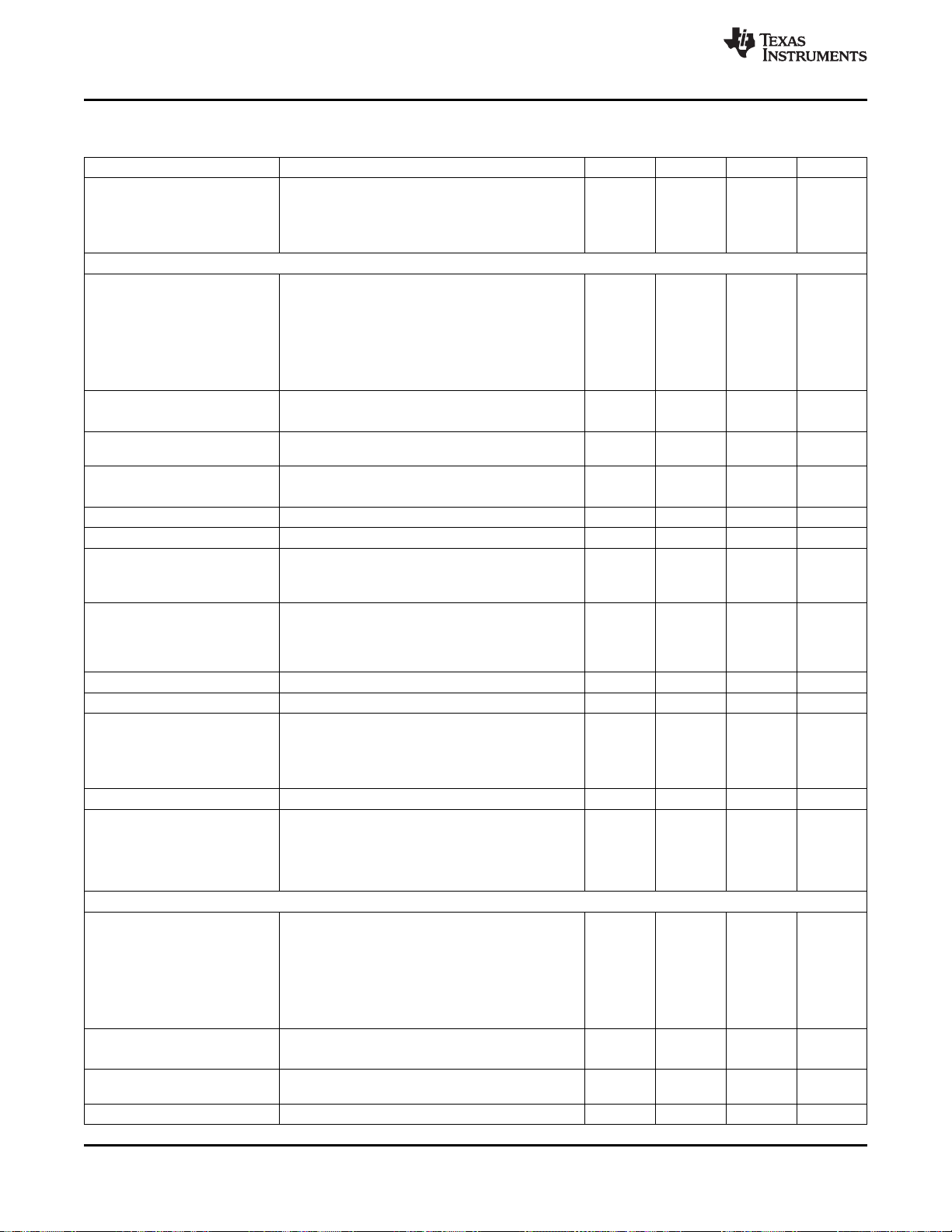
TPS65910, TPS65910A, TPS65910A3, TPS659101, TPS659102, TPS659103
TPS659104, TPS659105, TPS659106, TPS659107, TPS659108, TPS659109
SWCS046T –MARCH 2010–REVISED SEPTEMBER 2013
VDAC AND VPLL LDO
over operating free-air temperature range (unless otherwise noted)
PARAMETER TEST CONDITIONS MIN TYP MAX UNIT
V
(VDAC) = 1.8 V and V
Input voltage (VCC5) V
DC Output voltage V
OUT
Rated output current I
IN
OUTmax
OUT
/ 1.0 V
V
(VDAC) = 2.6 V and V
OUT
V
(VDAC) = 2.8 V / 2.85 V 3.2 5.5
OUT
On and low-power mode, VIN= V
SEL = 11, I
SEL = 10, I
SEL = 01, I
SEL = 00, I
00 or 01
OUT
OUT
OUT
OUT
= 0 to I
= 0 to I
= 0 to I
= 0 to I
On mode 150
Low-power mode 1
Load current limitation (shortcircuit protection)
Dropout Voltage V
DO
DC load regulation On mode, V
DC line regulation On mode, V
Transient load regulation 15 mV
Transient line regulation 0.5 mV
Turn-on time I
On mode, V
On mode, V
VIN= 2.9 V, I
= V
OUT
OUTmin
= 2.8 V, VDO= VIN– V
OUTtyp
= I
OUT
OUTmax
= V
OUT
OUTmin
= 1.8 V, I
OUT
On mode, VIN= 3.8 V, I
I
in 5 µs
OUTmax
And I
On mode, I
V
And VIN= V
I
OUTmax
OUT
INmin
= 0.9 × I
OUT
OUT
in 30 µs
/2
= 0, @ V
OUTmax
= I
OUTmax
to V
INmin
= 0.1 V up to V
OUT
INmin
Turn-on Inrush current 600 mA
Ripple Rejection
VIN= V
I
OUTmax
+ 100 mVpptone, V
INDC
/2
f = 217 Hz 70
f = 50 kHz 40
VDAC internal resistance LDO off 360 kΩ
Ground current On mode, I
On mode, I
= 0 60
OUT
= I
OUT
OUTmax
Low-power mode 12
Off mode 1
DC output voltage V
Rated output current I
OUT
OUTmax
On and low-power mode, VIN= V
SEL = 11, I
SEL = 10, I
or 01
SEL = 01, I
SEL = 00, I
OUT
OUT
OUT
OUT
= 0 to I
= 0 to I
= 0 to I
= 0 to I
On mode 50
Low-power mode 1
Load current limitation (shortcircuit protection)
Dropout voltage V
DO
On mode, V
On mode, V
= V
OUT
OUTmin
= 2.5 V, VDO= VIN– V
OUTtyp
(VPLL) = 1.8 V / 1.1 V
OUT
(VPLL) = 2.5 V 3.0 5.5
OUT
2.7 5.5
VDAC
to V
INmin
OUTmax
OUTmax
OUTmax
, default BOOT[1:0] =
OUTmax
INmax
–3% 2.85 +3%
–3% 2.8 +3%
–3% 2.6 +3%
–3% 1.8 +3%
– 100 mV 350 500 mA
, 150 mV
OUT
, T = 25°C
– 100 mV 15 mV
= I
OUT
OUTmax
= 0.1 × I
OUT
to 0.1 × I
, VIN= V
OUTmax
INmin
+ 0.5 V in 30 µs, I
OUTmin
INDC+
OUTmax
+ 0.5 V to
= 3.8 V, I
to 0.9 ×
in 5 µs
OUT
OUT
=
100 µs
=
1600
VPLL
to V
INmin
OUTmax
, default BOOT[1:0 = 00
OUTmax
OUTmax
OUTmax
INmax
–3% 2.5 +3%
–3% 1.8 +3%
–3% 1.1 +3%
–3% 1.0 +3%
– 100 mV 200 400 mA
, 100 mV
OUT
www.ti.com
2 mV
V
V
mA
dB
µA
V
mA
26 Submit Documentation Feedback Copyright © 2010–2013, Texas Instruments Incorporated
Product Folder Links: TPS65910 TPS65910A TPS65910A3 TPS659101 TPS659102 TPS659103 TPS659104
TPS659105 TPS659106 TPS659107 TPS659108 TPS659109
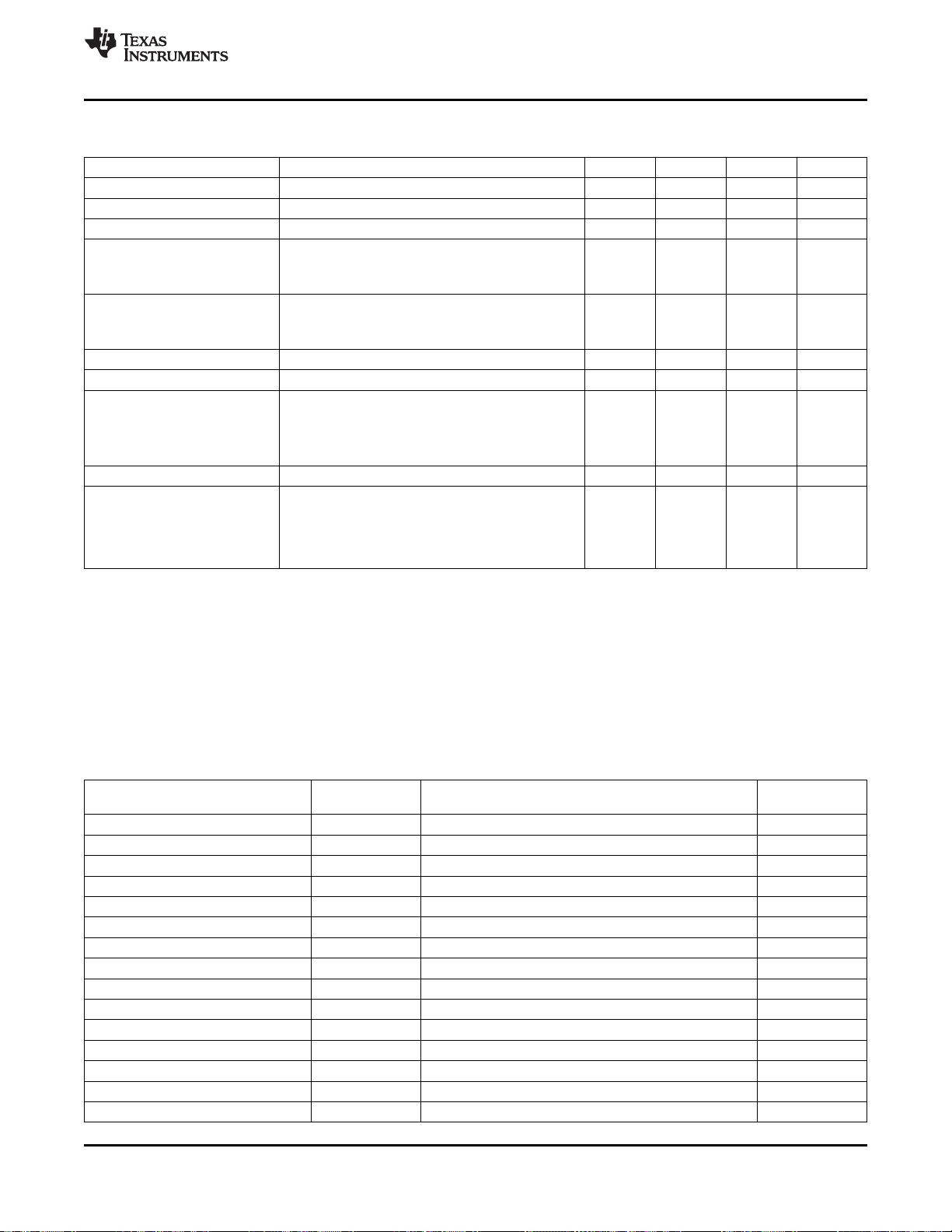
TPS65910, TPS65910A, TPS65910A3, TPS659101, TPS659102, TPS659103
TPS659104, TPS659105, TPS659106, TPS659107, TPS659108, TPS659109
www.ti.com
VDAC AND VPLL LDO (continued)
over operating free-air temperature range (unless otherwise noted)
PARAMETER TEST CONDITIONS MIN TYP MAX UNIT
VIN= 2.5 V, I
DC load regulation On mode, I
DC line regulation On mode, VIN= V
Transient load regulation 9 mV
On mode, VIN= 3.8 V, I
I
in 5 µs
OUTmax
And I
OUT
Transient line regulation On mode, VIN= V
And VIN= V
I
/2
OUTmax
Turn-on time I
OUT
= 0, @ V
Turn-on inrush current 300 mA
VIN= V
Ripple rejection
I
OUTmax
INDC
/2
f = 217 Hz 70
f = 50 kHz 40
VPLL internal resistance LDO off 535 kΩ
Ground current On mode, I
On mode, I
Low-power mode 12
Off mode 1
= I
OUT
= I
OUT
INmin
= 0.9 × I
OUTmax
INmin
to V
INmin
OUT
+ 100 mVpptone, V
= 0 60
OUT
= I
OUT
, T = 25°C
OUTmax
to 0 10 mV
OUTmax
to V
OUT
+ 0.5 V to V
INmin
= 0.1 V up to V
OUTmax
@ I
INmax
to 0.1 × I
= 0.1 × I
OUT
OUTmax
OUTmax
in 30 µs 0.5 mV
INmin
+ 0.5 V in 30 µs, I
OUTmin
= 3.8 V, I
INDC+
= I
OUTmax
to 0.9 ×
in 5 µs
OUT
SWCS046T –MARCH 2010–REVISED SEPTEMBER 2013
1 mV
=
100 µs
=
OUT
1600
dB
µA
SWITCH-ON/-OFF SEQUENCES AND TIMING
Time slot length can be selected to be 0.5 ms or 2 ms through the EEPROM for an OFF-to-ACTIVE transition or
through the value programmed in the register DEVCTRL2_REG for a SLEEP-to-ACTIVE transition.
BOOT1 = 0, BOOT0 = 0
Table 2 provides details about the EEPROM setting for the BOOT modes. The power-up sequence for this boot
mode is provided in Figure 2.
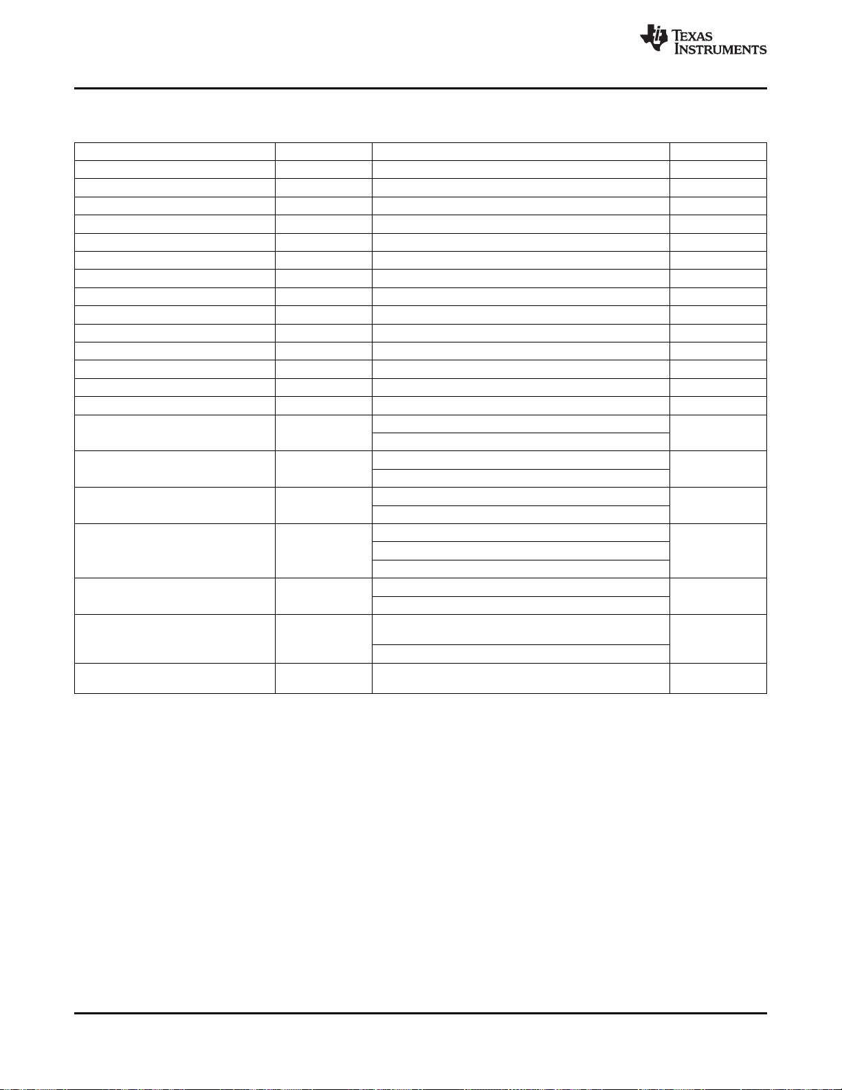
Table 2. Fixed Boot Mode: 00
Register Bit Description
VDD1_OP_REG SEL VDD1 voltage level selection for boot 1.2 V
VDD1_REG VGAIN_SEL VDD1 Gain selection, x1 or x2 x1
EEPROM VDD1 time slot selection 3
DCDCCTRL_REG VDD1_PSKIP VDD1 pulse skip mode enable skip enabled
VDD2_OP_REG/VDD2_SR_REG SEL VDD2 voltage level selection for boot 1.1 V
VDD2_REG VGAIN_SEL VDD2 Gain selection, x1 or x3 x3
EEPROM VDD2 time slot selection 2
DCDCCTRL_REG VDD2_PSKIP VDD2 pulse skip mode enable skip enabled
VIO_REG SEL VIO voltage selection 1.8 V
EEPROM VIO time slot selection 1
DCDCCTRL_REG VIO_PSKIP VIO pulse skip mode enable skip enabled
EEPROM VDD3 time slot OFF
VDIG1_REG SEL LDO voltage selection 1.2 V
EEPROM LDO time slot OFF
VDIG2_REG SEL LDO voltage selection 1.0 V
TPS65910
Boot 00
Copyright © 2010–2013, Texas Instruments Incorporated Submit Documentation Feedback 27
Product Folder Links: TPS65910 TPS65910A TPS65910A3 TPS659101 TPS659102 TPS659103 TPS659104
TPS659105 TPS659106 TPS659107 TPS659108 TPS659109
TPS65910, TPS65910A, TPS65910A3, TPS659101, TPS659102, TPS659103
TPS659104, TPS659105, TPS659106, TPS659107, TPS659108, TPS659109
SWCS046T –MARCH 2010–REVISED SEPTEMBER 2013
SWITCH-ON/-OFF SEQUENCES AND TIMING (continued)
Table 2. Fixed Boot Mode: 00 (continued)
EEPROM LDO time slot OFF
VDAC_REG SEL LDO voltage selection 1.8 V
EEPROM LDO time slot 5
VPLL_REG SEL LDO voltage selection 1.8 V
EEPROM LDO time slot 4
VAUX1_REG SEL LDO voltage selection 1.8 V
EEPROM LDO time slot 1
VMMC_REG SEL LDO voltage selection 3.3 V
EEPROM LDO time slot 6
VAUX33_REG SEL LDO voltage selection 1.8 V
EEPROM LDO time slot OFF
VAUX2_REG SEL LDO voltage selection 1.8 V
EEPROM LDO time slot 5
CLK32KOUT pin CLK32KOUT time slot 7
NRESPWRON pin NRESPWRON time slot 7 + 1
VRTC_REG Low-power mode
DEVCTRL_REG RTC_PWDN 1
DEVCTRL_REG CK32K_CTRL RC
DEVCTRL2_REG 0: 0.5 ms 2 ms
DEVCTRL2_REG IT_POL Active-low
INT_MSK_REG VMBHI_IT_MSK switch-on from
VMBCH_REG VMBCH_SEL[1:0] 3 V
VRTC_OFFMAS
K
TSLOT_LENGTH
[0]
0: VRTC LDO will be in low-power mode during OFF state
1: VRC LDO will be in full-power mode during OFF state
0: RTC in normal power mode
1: Clock gating of RTC register and logic, low-power mode
0: Clock source is crystal/external clock
1: Clock source is internal RC oscillator
Boot sequence time slot duration:
1: 2 ms
0: INT1 signal will be active-low
1: INT1 signal will be active-high
0: Device will automatically switch-on at NOSUPPLY to
OFF or BACKUP to OFF transition
1: Startup reason required before switch-on
Select threshold for main battery comparator threshold
VMBCH.
www.ti.com
0: Automatic
supply insertion
28 Submit Documentation Feedback Copyright © 2010–2013, Texas Instruments Incorporated
Product Folder Links: TPS65910 TPS65910A TPS65910A3 TPS659101 TPS659102 TPS659103 TPS659104
TPS659105 TPS659106 TPS659107 TPS659108 TPS659109
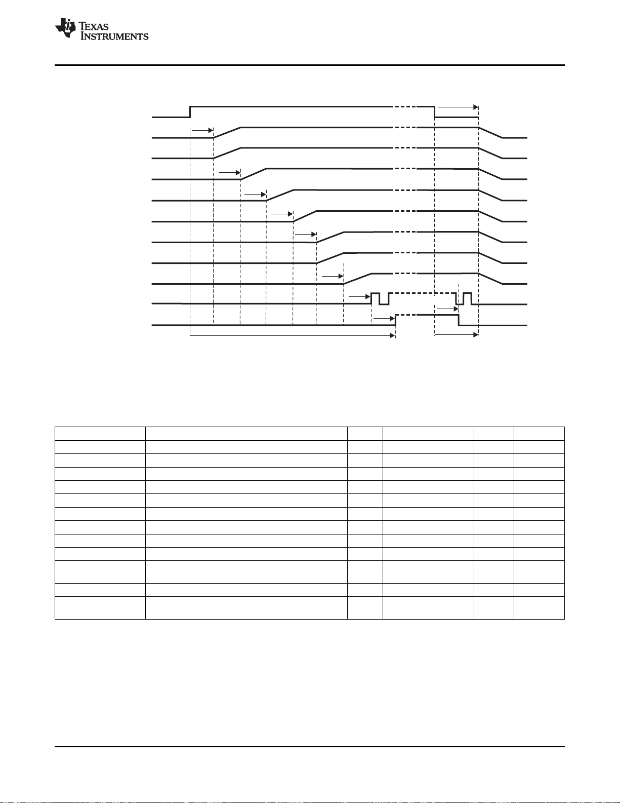
SWCS046-018
PWRHOLD
VIO/VFBIO
VAUX1
VDD2/VFB2
VDD1/VFB1
VPLL
VDAC
VAUX2
VMMC
CLK32KOUT
NRESPWRON
t
dSOFF2
t
dSON1
1.8 V
1.8 V
3.3 V
t
dSON2
t
dSON3
1.2 V
1.8 V
1.8 V
t
dSON4
t
dSON5
1.8 V
t
dSON6
t
dSON7
3.3 V
t
dSON8
t
dSOFF1
Switch-off sequence
t : Switch-on sequence
dSONT
TPS65910, TPS65910A, TPS65910A3, TPS659101, TPS659102, TPS659103
TPS659104, TPS659105, TPS659106, TPS659107, TPS659108, TPS659109
www.ti.com
Figure 2 shows the 00 Boot mode timing characteristics.
SWCS046T –MARCH 2010–REVISED SEPTEMBER 2013
Figure 2. Boot Mode: BOOT1 = 0, BOOT0 = 0
Table 3 lists the 00 Boot mode timing characteristics.
Table 3. Boot Mode: BOOT1 = 0, BOOT0 = 0 Timing Characteristics
PARAMETER TEST CONDITIONS MIN TYP MAX UNIT
t
dSON1
t
dSON2
t
dSON3
t
dSON4
t
dSON5
t
dSON6
t
dSON8
t
dSONT
t
dSOFF1
t
dSOFF1B
t
dSOFF2
PWRHOLD rising edge to VIO, VAUX1 enable delay 66 × t
VIO to VDD2 enable delay 64 × t
VDD2 to VDD1 enable delay 64 × t
VDD1 to VPLL enable delay 64 × t
VPLL to VDAC,VAUX2 enable delay 64 × t
VDAC to VMMC enable delay 64 × t
VMMC to CLK32KOUT rising edge delay 64 × t
CLK32KOUT to NRESPWRON rising edge delay 64 × t
Total switch-on delay 16 ms
PWRHOLD falling edge to NRESPWRON falling edge
delay
2 × t
NRESPWRON falling edge to CLK32KOUT low delay 3 × t
PWRHOLD falling edge to supplies and reference
disable delay
5 × t
= 2060 µs
CK32k
= 2000 µs
CK32k
= 2000 µs
CK32k
= 2000 µs
CK32k
= 2000 µs
CK32k
= 2000 µs
CK32k
= 2000 µs
CK32k
= 2000 µs
CK32k
= 62.5 µs
CK32k
= 92 µs
CK32k
= 154 µs
CK32k
Registers default setting: CK32K_CTRL = 1 (32-kHz RC oscillator is used), RTC_PWDN = 1 (RTC domain off),
IT_POL = 0 (INt2 interrupt flag active low), VMBHI_IT_MSK = 0 (automatic switch-on on Battery plug),
VMBCH_SEL = 11.
BOOT1 = 0, BOOT0 = 1
Table 4 provides details about the EEPROM setting for the BOOT modes. The power-up sequence for this boot
mode is provided in Figure 3.
Copyright © 2010–2013, Texas Instruments Incorporated Submit Documentation Feedback 29
Product Folder Links: TPS65910 TPS65910A TPS65910A3 TPS659101 TPS659102 TPS659103 TPS659104
TPS659105 TPS659106 TPS659107 TPS659108 TPS659109
TPS65910, TPS65910A, TPS65910A3, TPS659101, TPS659102, TPS659103
TPS659104, TPS659105, TPS659106, TPS659107, TPS659108, TPS659109
SWCS046T –MARCH 2010–REVISED SEPTEMBER 2013
Table 4. Fixed Boot Mode: 01
Register Bit Description
VDD1_OP_REG SEL VDD1 voltage level selection for boot 1.2 V
VDD1_REG VGAIN_SEL VDD1 Gain selection, x1 or x2 x1
EEPROM VDD1 time slot selection 3
DCDCCTRL_REG VDD1_PSKIP VDD1 pulse skip mode enable Skip enabled
VDD2_OP_REG/VDD2_SR_REG SEL VDD2 voltage level selection for boot 1.2 V
VDD2_REG VGAIN_SEL VDD2 Gain selection, x1 or x3 x1
EEPROM VDD2 time slot selection 4
DCDCCTRL_REG VDD2_PSKIP VDD2 pulse skip mode enable Skip enabled
VIO_REG SEL VIO voltage selection 1.8 V
EEPROM VIO time slot selection 1
DCDCCTRL_REG VIO_PSKIP VIO pulse skip mode enable Skip enabled
EEPROM VDD3 time slot OFF
VDIG1_REG SEL LDO voltage selection 1.2 V
EEPROM LDO time slot OFF
VDIG2_REG SEL LDO voltage selection 1.0 V
EEPROM LDO time slot OFF
VDAC_REG SEL LDO voltage selection 1.8 V
EEPROM LDO time slot OFF
VPLL_REG SEL LDO voltage selection 1.8 V
EEPROM LDO time slot 2
VAUX1_REG SEL LDO voltage selection 1.8 V
EEPROM LDO time slot OFF
VMMC_REG SEL LDO voltage selection 1.8 V
EEPROM LDO time slot OFF
VAUX33_REG SEL LDO voltage selection 3.3 V
EEPROM LDO time slot 6
VAUX2_REG SEL LDO voltage selection 1.8 V
EEPROM LDO time slot 5
CLK32KOUT pin CLK32KOUT time slot 7
NRESPWRON pin NRESPWRON time slot 7+1
VRTC_REG low-power mode
DEVCTRL_REG RTC_PWDN 1
DEVCTRL_REG CK32K_CTRL Crystal
DEVCTRL2_REG 0: 0.5 ms 2 ms
DEVCTRL2_REG IT_POL Active-low
INT_MSK_REG VMBHI_IT_MSK switch-on from
VMBCH_REG VMBCH_SEL[1:0] 3 V
VRTC_OFFMAS
K
TSLOT_LENGTH
[0]
0: VRTC LDO will be in low-power mode during OFF state
1: VRC LDO will be in full-power mode during OFF state
0: RTC in normal power mode
1: Clock gating of RTC register and logic, low-power mode
0: Clock source is crystal/external clock
1: Clock source is internal RC oscillator
Boot sequence time slot duration:
1: 2 ms
0: INT1 signal will be active-low
1: INT1 signal will be active-high
0: Device will automatically switch-on at NOSUPPLY to
OFF or BACKUP to OFF transition
1: Startup reason required before switch-on
Select threshold for main battery comparator threshold
VMBCH.
www.ti.com
TPS65910
Boot 01
0: Automatic
supply insertion
30 Submit Documentation Feedback Copyright © 2010–2013, Texas Instruments Incorporated
Product Folder Links: TPS65910 TPS65910A TPS65910A3 TPS659101 TPS659102 TPS659103 TPS659104
TPS659105 TPS659106 TPS659107 TPS659108 TPS659109
 Loading...