

Page 1
www.ti.com
COMP
VINB
FREQ
EN1
EN2
DRN
FBN
REF
PGND
PGND
SW
SW
AVIN
FB
GND
OS
DRP
FBP
Boot
SWB
NC
DLY1
TPS65160
SS
VINB
GD
FBB
DLY2
SUP
12 V
C1
2*22 F
C3
1 F
C16
1 F
C6
0.47 FD2
D3
VGL
−5 V/50 mA
R3
620 k
R4
150 k
C8
220 nF
C7
470 F
C9
22 nF
C10
10 nF
C11
10 nF
C17
22 nF
R8
1.2 k
R7
2 k
D6
SL22
L2
15 H
Cb
100 nF
R6
56 k
C14
10 nF
C12
2*22 F
3.3 V/1.5 A
C13
0.47 F
R5
1 M
VGH
23 V/50 mA
D5
D4
GD
0.47 F
C5
C15
470 nF
R2
56 k
R1
680 k
C2
3* 22 F
C4
22 pF
D1
SL22
L1
10 H
15 V/1.5 A
8
12
20
21
22
16
9
11
13
24
6
7
28
25
4
5
1
3
23
27
10
14
17
18
19
15
2
26
V
IN
V
LOGIC
V
S
BIAS POWER SUPPLY FOR TV AND MONITOR TFT LCD PANELS
TPS65160, TPS65160A
SLVS566B – MARCH 2005 – REVISED JULY 2005
FEATURES
• Gate Drive Signal to Drive External MOSFET
• 8-V to 14-V Input Voltage Range • Internal and Adjustable Soft Start
• V
Output Voltage Range up to 20 V • Short-Circuit Protection
S
• 1% Accurate Boost Converter With 2.8-A • 23-V (TPS65160) Overvoltage Protection
Switch Current
• 1.5% accurate 1.8-A Step-Down Converter
• 500-kHz/750-kHz Fixed Switching Frequency
• 19.5-V (TPS65160A) Overvoltage Protection
• Thermal Shutdown
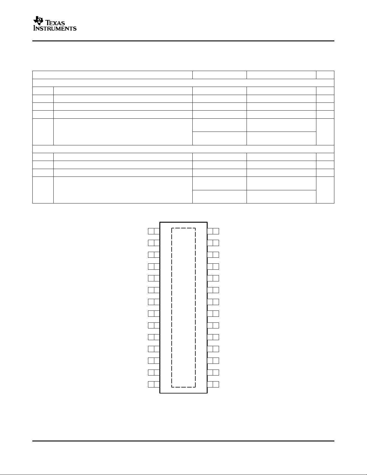
• Available in TSSOP-28 Package
• Negative Charge Pump Driver for VGL
• Positive Charge Pump Driver for VGH
• Adjustable Sequencing for VGL, VGH
APPLICATIONS
• TFT LCD Displays for Monitor and LCD TV
DESCRIPTION
The TPS65160 offers a compact power supply solution to provide all four voltages required by thin-film transistor
(TFT) LCD panel. With its high current capabilities, the device is ideal for large screen monitor panels and LCD
TV applications.
TYPICAL APPLICATION
Please be aware that an important notice concerning availability, standard warranty, and use in critical applications of Texas
Instruments semiconductor products and disclaimers thereto appears at the end of this data sheet.
PowerPAD is a trademark of Texas Instruments.
PRODUCTION DATA information is current as of publication date.
Products conform to specifications per the terms of the Texas
Instruments standard warranty. Production processing does not
necessarily include testing of all parameters.
Copyright © 2005, Texas Instruments Incorporated
Page 2
www.ti.com
TPS65160, TPS65160A
SLVS566B – MARCH 2005 – REVISED JULY 2005
DESCRIPTION (CONTINUED)
The device can be powered directly from a 12-V input voltage generating the bias voltages VGH and VGL, as
well as the source voltage V
provide the source voltage V
and a negative charge-pump driver provide adjustable regulated output voltages VGL and VGH to bias the TFT.
Both boost and step-down converters, as well as the charge-pump driver, operate with a fixed switching
frequency of 500 kHz or 750 kHz, selectable by the FREQ pin. The TPS65160 includes adjustable power-on
sequencing. The device includes safety features like overvoltage protection of the boost converter and
short-circuit protection of the buck converter, as well as thermal shutdown. Additionally, the device incorporates a
gate drive signal to control an isolation MOSFET switch in series with V
the end of this data sheet.
This integrated circuit can be damaged by ESD. Texas Instruments recommends that all integrated
circuits be handled with appropriate precautions. Failure to observe proper handling and installation
procedures can cause damage.
ESD damage can range from subtle performance degradation to complete device failure. Precision
integrated circuits may be more susceptible to damage because very small parametric changes could
cause the device not to meet its published specifications.
and logic voltage for the LCD panels. The device consists of a boost converter to
S
and a step-down converter to provide the logic voltage for the system. A positive
S
or VGH. See the application circuits at
S
ORDERING INFORMATION
T
A
–40 ° C to 85 ° C
(1) For the most current package and ordering information, see the Package Option Addendum at the end of this document, or see the TI
Web site at www.ti.com .
(2) The PWP package is available taped and reeled. Add R-suffix to the device type (TPS65160PWPR) to order the device taped and
reeled. The TPS65160PWPR package has quantities of 2000 devices per reel. Without suffix, the TPS65160PWP is shipped in tubes
with 50 devices per tube.
UVLO Overvoltage protection ORDERING PACKAGE
(typ) Vs (typ) MARKING
6 V 23 V TPS65160PWP TSSOP28 (PWP) TPS65160
8 V 19.5 V TPS65160APWP TSSOP28 (PWP) TPS65160A
(1)
(2)
PACKAGE
ABSOLUTE MAXIMUM RATINGS
over operating free-air temperature range (unless otherwise noted)
Voltages on pin VIN, SUP
Voltages on pin EN1, EN2, FREQ
Voltage on pin SW
Voltage on pin SWB
Voltages on pin OS, GD
Continuous power dissipation See Dissipation Rating Table
T
A
T
stg
(1) Stresses beyond those listed under absolute maximum ratings may cause permanent damage to the device. These are stress ratings
(2) All voltage values are with respect to network ground terminal.
Operating junction temperature –40 ° C to 150 ° C
Storage temperature range –65 ° C to 150 ° C
Temperature (soldering, 10 s) 260 ° C
only, and functional operation of the device at these or any other conditions beyond those indicated under recommended operating
conditions is not implied. Exposure to absolute-maximum-rated conditions for extended periods may affect device reliability.
(2)
(2)
(2)
(2)
(2)
(1)
UNIT
–0.3 V to 16.5 V
–0.3 V to 15 V
25 V
20 V
25 V
DISSIPATION RATINGS
PACKAGE RTH
28-Pin TSSOP 28 ° C/W (PowerPAD
(1) See Texas Instruments application report SLMA002 regarding thermal characteristics of the PowerPAD package.
2
JA
(1)
soldered) 3.57 W 1.96 W 1.42 W
TA≤ 25 ° C TA= 70 ° C TA= 85 ° C
POWER RATING POWER RATING POWER RATING
Page 3
www.ti.com
TPS65160, TPS65160A
SLVS566B – MARCH 2005 – REVISED JULY 2005
RECOMMENDED OPERATING CONDITIONS
over operating free-air temperature range (unless otherwise noted)
MIN NOM MAX UNIT
V
S
V
SUP
C
IN
L µH
V
LOGIC
C
O
T
A
T
J
(1) See application section for further information.
ELECTRICAL CHARACTERISTICS
V
IN
(unless otherwise noted)
SUPPLY CURRENT
V
IN
I
QIN
I
SD
I
SUP
V
UVLO
V
REF
LOGIC SIGNALS EN1, EN2, FREQ
V
IH
V
IL
V
IH
V
IL
I
I
CONTROL AND SOFT START DLY1, DLY2, SS
I
DLY1
I
DLY2
I
SS
Output voltage range of the main boost converter TPS65160 20 V
TPS65160A 17.5 V
Maximum operating voltage at the charge-pump driver supply pin SUP 15 V
Input capacitor at VINB 2x22 µF
Input capacitor AVIN 1 µF
Inductor boost converter
Inductor buck converter
Output voltage range of the step-down converter V
(1)
(1)
LOGIC
1.8 5.0 V
10
15
Output capacitor boost converter 3x22
Output capacitor buck converter 2x22
Operating ambient temperature –40 85 ° C
Operating junction temperature –40 125 ° C
= 12 V, SUP = VIN, EN1 = EN2 = VIN, VS= 15 V, V
= 3.3 V, TA= –40 ° C to 85 ° C, typical values are at TA= 25 ° C
LOGIC
PARAMETER TEST CONDITIONS MIN TYP MAX UNIT
Input voltage range
TPS65160 8 14 V
TPS65160A 9.2 14 V
VGH = 2 x VS, 0.2 2
Quiescent current into AVIN Boost converter not
switching
VGH = 2 x VS, 0.2 0.5
Quiescent current into VINB Buck converter not
switching
Shutdown current into AVIN EN1 = EN2 = GND 0.1 2
Shutdown current into VINB EN1 = EN2 = GND 0.1 2
Shutdown current into SUP EN1 = EN2 = GND 0.1 4 µA
Quiescent current into SUP VGH = 2 x V
Undervoltage lockout threshold
TPS65160 VINfalling 6 6.4 V
TPS65160A VINfalling 8 8.8 V
S
0.2 2 mA
Reference voltage 1.203 1.213 1.223 V
Thermal shutdown Temperature rising 155 ° C
Thermal shutdown hysteresis 5 ° C
High-level input voltage EN1, EN2 2.0 V
Low-level input voltage EN1, EN2 0.8 V
High-level input voltage FREQ 1.7 V
Low-level input voltage FREQ 0.4 V
Input leakage current
EN1 = EN2 = FREQ = 0.01 0.1 µA
GND or V
IN
Delay1 charge current 3.3 4.8 6.2 µA
Delay2 charge current V
THRESHOLD
= 1.213 V 3.3 4.8 6.2 µA
SS charge current 6 9 12 µA
µF
mA
µA
3
Page 4
www.ti.com
TPS65160, TPS65160A
SLVS566B – MARCH 2005 – REVISED JULY 2005
ELECTRICAL CHARACTERISTICS (continued)
V
= 12 V, SUP = VIN, EN1 = EN2 = VIN, VS= 15 V, V
IN
(unless otherwise noted)
PARAMETER TEST CONDITIONS MIN TYP MAX UNIT
INTERNAL OSCILLATOR
f
OSC
BOOST CONVERTER (VS)
V
V
I
FB
r
DS(ON)
I
MAX
I
LIM
Ileak Switch leakage current V
Vovp Overvoltage protection
GATE DRIVE (GD)
V
V
STEP-DOWN CONVERTER (V
V
V
I
FBB
r
DS(ON)
I
LIM
Ileak Switch leakage current V
(1) The GD signal is latched low when the main boost converter output VSis within regulation. The GD signal is reset when the input
Oscillator frequency kHz
Output voltage range
S
Feedback regulation voltage 1.136 1.146 1.156 V
FB
TPS65160 20 V
TPS65160A 17.5 V
Feedback input bias current 10 100 nA
N-MOSFET on-resistance (Q1) ISW= 500 mA 100 185 m Ω
P-MOSFET on-resistance (Q2) ISW= 200 mA 10 16 Ω
Maximum P-MOSFET peak switch current 1 A
N-MOSFET switch current limit (Q1) 2.8 3.5 4.2 A
TPS65160 V
TPS65160A V
Line regulation
Load regulation 0.03 %/A
Gate drive threshold
GD
GD output low voltage I
OL
(1)
GD output leakage current VGD = 20 V 0.05 1 µA
)
LOGIC
Output voltage range 1.8 5 V
LOGIC
Feedback regulation voltage 1.195 1.213 1.231 V
FBB
Feedback input bias current 10 100 nA
N-MOSFET on-resistance (Q1) ISW= 500 mA 175 300 m Ω
N-MOSFET switch current limit (Q1) 2 2.6 3.3 A
Line regulation
Load regulation 0.037 %/A
voltage or enable of the boost converter is cycled low.
= 3.3 V, TA= –40 ° C to 85 ° C, typical values are at TA= 25 ° C
LOGIC
FREQ = high 600 750 900
FREQ = low 400 500 600
= 15 V 1 10 µA
SW
rising 22 23 24.5 V
OUT
rising 18 19.5 20.5 V
OUT
10.6 V ≤ Vin ≤ 11.6 V 0.0008 %/V
at 1 mA
V
rising Vs-12% Vs-8% Vs-4% V
FB
= 500 µA 0.3 V
(sink)
= 0 V 1 10 µA
SW
10.6 V ≤ VIN≤ 11.6 V 0.0018 %/V
at 1 mA
4
Page 5
www.ti.com
1
2
3
4
5
6
7
8
9
10
11
12
28
27
26
25
24
23
22
21
20
19
18
17
FB
COMP
OS
SW
SW
PGND
PGND
SUP
EN2
DRP
DRN
FREQ
SS
GD
DLY2
DLY1
REF
GND
AVIN
VINB
VINB
NC
SWB
BOOT
Thermal PAD (see Note)
13
14
16
15
FBN
FBP
EN1
FBB
TPS65160, TPS65160A
SLVS566B – MARCH 2005 – REVISED JULY 2005
ELECTRICAL CHARACTERISTICS (continued)
V
= 12 V, SUP = VIN, EN1 = EN2 = VIN, VS= 15 V, V
IN
(unless otherwise noted)
PARAMETER TEST CONDITIONS MIN TYP MAX UNIT
NEGATIVE CHARGE-PUMP VGL
VGL Output voltage range –2 V
V
I
FBN
r
DS(ON)
V
POSITIVE CHARGE-PUMP OUTPUT VGH
V
I
FBP
r
DS(ON)
V
Feedback regulation voltage –36 0 36 mV
FBN
Feedback input bias current 10 100 nA
Q4 P-Channel switch r
Current sink voltage drop
DropN
Feedback regulation voltage 1.187 1.213 1.238 V
FBP
Feedback input bias current 10 100 nA
Q3 N-Channel switch r
Current source voltage drop
DropP
(Vsup – V
)
DRP
DS(ON)
(2)
DS(ON)
(2)
= 3.3 V, TA= –40 ° C to 85 ° C, typical values are at TA= 25 ° C
LOGIC
I
= 20 mA 4.4 Ω
OUT
I
= 50 mA, 130 190
DRN
V
= V
FBN
FBNnominal
I
= 100 mA, 270 420
DRN
V
= V
FBN
FBNnominal
I
= 20 mA 1.1 Ω
OUT
I
= 50 mA, 400 680
DRP
V
= V
FBP
FBPnominal
I
= 100 mA, 850 1600
DRP
V
= V
FBP
FBPnominal
–5%
–5%
–5%
–5%
mV
mV
(2) The maximum charge-pump output current is typically half the drive current of the internal current source or current sink.
NOTE: The thermally enhanced PowerPAD™ is connected to PGND.
5
Page 6
www.ti.com
TPS65160, TPS65160A
SLVS566B – MARCH 2005 – REVISED JULY 2005
TERMINAL FUNCTIONS
TERMINAL
NAME NO.
SUP 8 I of the TPS65160 main boost converter. Because the SUP pin is rated to a maximum voltage of 15 V, it needs to
FREQ 12 I
AVIN 22 I
VINB 20, 21 I Power input voltage pin for the buck converter.
EN1 16 I converter starts up, and after a delay time set by DLY1, the negative charge pump comes up. This pin must be
EN2 9 I charge pump starts up after the buck converter is within regulation and a delay time set by DLY2 has passed by.
DRN 11 O Drive pin of the negative charge pump.
FBN 13 I Feedback pin of negative charge pump.
REF 24 O Internal reference output typically 1.213 V
PGND 6, 7 Power ground
SS 28 O
DLY1 25 O
DLY2 26 O
COMP 2
FBB 15 I Feedback pin of the buck converter
SWB 18 O Switch pin of the buck converter
NC 19 Not connected
BOOT 17 I
FBP 14 I Feedback pin of positive charge pump.
DRP 10 O Drive pin of the positive charge pump.
GD 27
GND 23 Analog ground
OS 3 I
FB 1 I Feedback of the main boost converter generating Vsource (V
SW 4, 5 I Switch pin of the boost converter generating Vsource (VS).
PowerPAD The PowerPAD needs to be connected and soldered to power ground (PGND).
I/O DESCRIPTION
This is the supply pin of the positive and negative charge-pump driver and can be connected to the input or output
be connected to the input of the TPS65160 for an output voltage greater than 15 V.
Frequency adjust pin. This pin allows setting the switching frequency with a logic level to 500 kHz = low and
750 kHz = high.
Analog input voltage of the device. This is the input for the analog circuits of the device and should be bypassed
with a 1- µ F ceramic capacitor for good filtering.
This is the enable pin of the buck converter and negative charge pump. When this pin is pulled high, the buck
terminated and not be left floating. A logic high enables the device and a logic low shuts down the device.
The boost converter starts only with EN1 = high, after the step-down converter is enabled. EN2 is the enable pin
of the boost converter and positive charge pump. When this pin is pulled high, the boost converter and positive
This pin must be terminated and not be left floating. A logic high enables the device and a logic low shuts down
the device.
This pin allows setting the soft-start time for the main boost converter VS. Typically a 22-nF capacitor needs to be
connected to this pin to set the soft-start time.
Connecting a capacitor from this pin to GND allows the setting of the delay time between V
converter output high) to VGL during start-up.
Connecting a capacitor from this pin to GND allows the setting of the delay time between V
converter output high) to VSBoost converter and positive charge-pump VGH during start-up.
This is the compensation pin for the main boost converter. A small capacitor and, if required, a resistor is
connected to this pin.
N-channel MOSFET gate drive voltage for the buck converter. Connect a capacitor from the switch node SWB to
this pin.
This is the gate drive pin which can be used to control an external MOSFET switch to provide input to output
isolation of VSor VGH. See the circuit diagrams at the end of this data sheet. GD is an open-drain output and is
latched low as soon as the boost converter is within 8% of its nominal regulated output voltage. GD goes high
impedance when the EN2 input voltage is cycled low.
Output sense pin. The OS pin is connected to the internal rectifier switch and overvoltage protection comparator.
This pin needs to be connected to the output of the boost converter and cannot be connected to any other voltage
rail. Connect a 470-nF capacitor from OS pin to GND to avoid noise coupling into this pin. The PCB trace of the
OS pin needs to be wide because it conducts high current.
).
S
LOGIC
LOGIC
(step-down
(step-down
6
Page 7
www.ti.com
TYPICAL CHARACTERISTICS
0
0.02
0.04
0.06
0.08
0.1
0.12
0.14
0.16
−40 −20 0 20 40 60 80 100 120 140
r
DS(on)
− N-Channel Switch −
TA − Temperature − C
Ω
VI = 8 V ,
VI = 12 V ,
VI = 14 V
0
10
20
30
40
50
60
70
80
90
100
0 0.5 1 1.5 2
VI = 12 V ,
VO = 15 V ,
L = 10 H
IO − Output Current − A
Efficiency − %
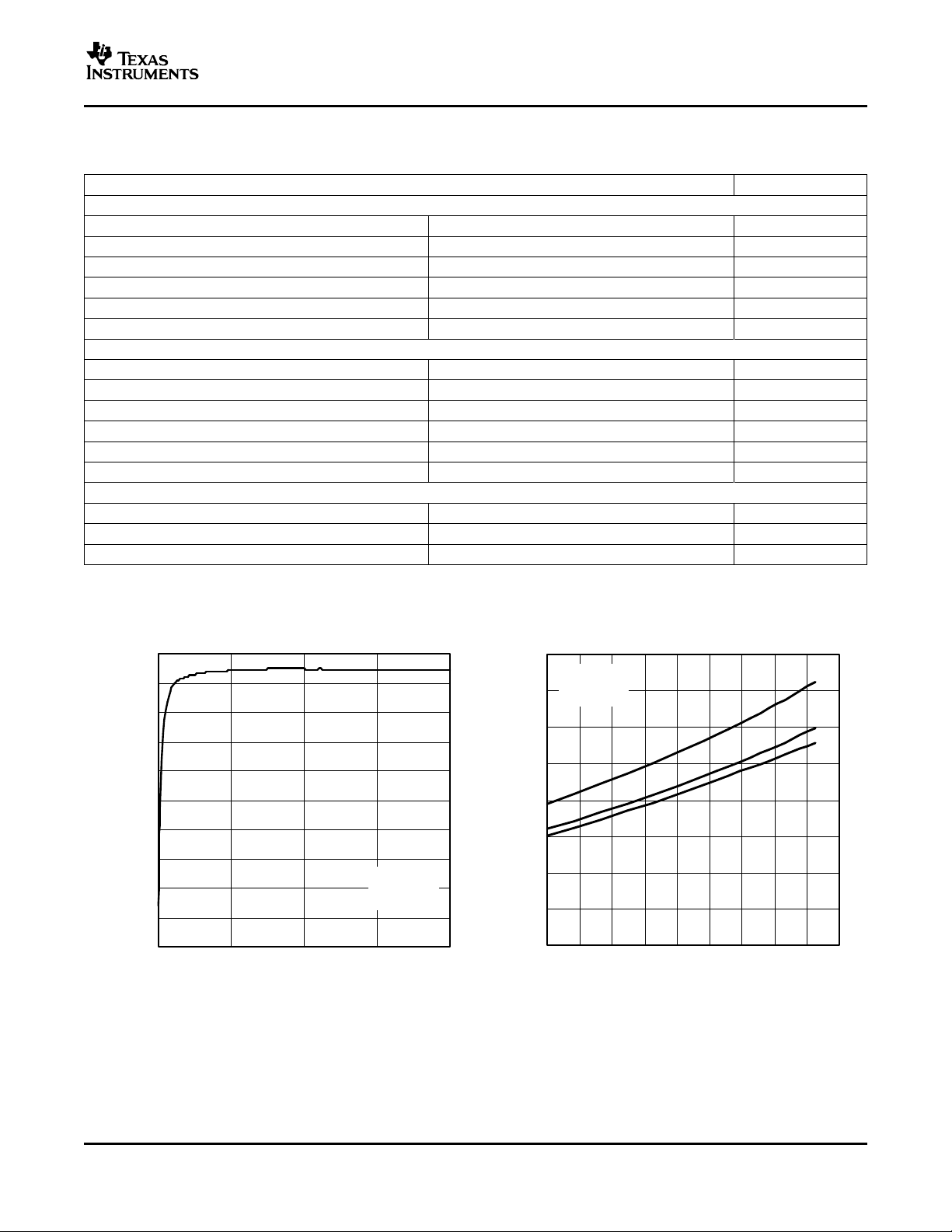
TABLE OF GRAPHS
MAIN BOOST CONVERTER (Vs)
η Efficiency main boost converter Vs vs Load current VS=15 V,V
r
DS(ON)
STEP-DOWN CONVERTER (Vlogic)
η Efficiency main boost converter V
r
DS(ON)
SYSTEM PERFORMANCE
f
osc
N-channel main switch Q1 vs Input voltage and temperature 2
Soft-start boost converter C
= 22 nF 3
SS
PWM operation at full-load current 4
PWM operation at light-load current 5
Load transient response 6
S
vs Load current V
LOGIC
N-channel main switch Q1 8
PWM operation - continuous mode 9
PWM operation - discontinuous mode 10
Soft start 11
Load transient response 12
Oscillation frequency vs Input voltage and temperature 13
Power-up sequencing EN2 connected to V
Power-up sequencing EN2 enabled seperately 15
TPS65160, TPS65160A
SLVS566B – MARCH 2005 – REVISED JULY 2005
FIGURE
= 12 V 1
IN
= 3.3 V,V
IN
= 12 V 7
IN
14
BOOST CONVERTER EFFICIENCY BOOST CONVERTER
vs r
OUTPUT CURRENT vs
Figure 1. Figure 2.
- N-CHANNEL SWITCH
DS(ON)
TEMPERATURE
7
Page 8
www.ti.com
V
S
5 V/div
I
I
1 A/div
VI = 12 V ,
VO = 15 V/ 1.2 A,
C
(SS)
= 22 nF
2 ms/div
V
SW
10 V/div
V
O
50 mV/div
I
(Inductor)
1 A/div
1 s/div
VI = 12 V ,
VO = 15 V/1.5 A
VI = 12 V , VS = 15 V ,
CO = 3*22 F,
C
(comp)
= 22 nF,
L = 6.8 H,
FREQ= High
V
S
200 mV/div
100 s/div
I
(Inductor)
1 A/div
V
SW
10 V/div
V
O
50 mV/div
I
L
500 mA/div
1 s/div
VI = 3.3 V ,
VO = 10 V/10 mA
TPS65160, TPS65160A
SLVS566B – MARCH 2005 – REVISED JULY 2005
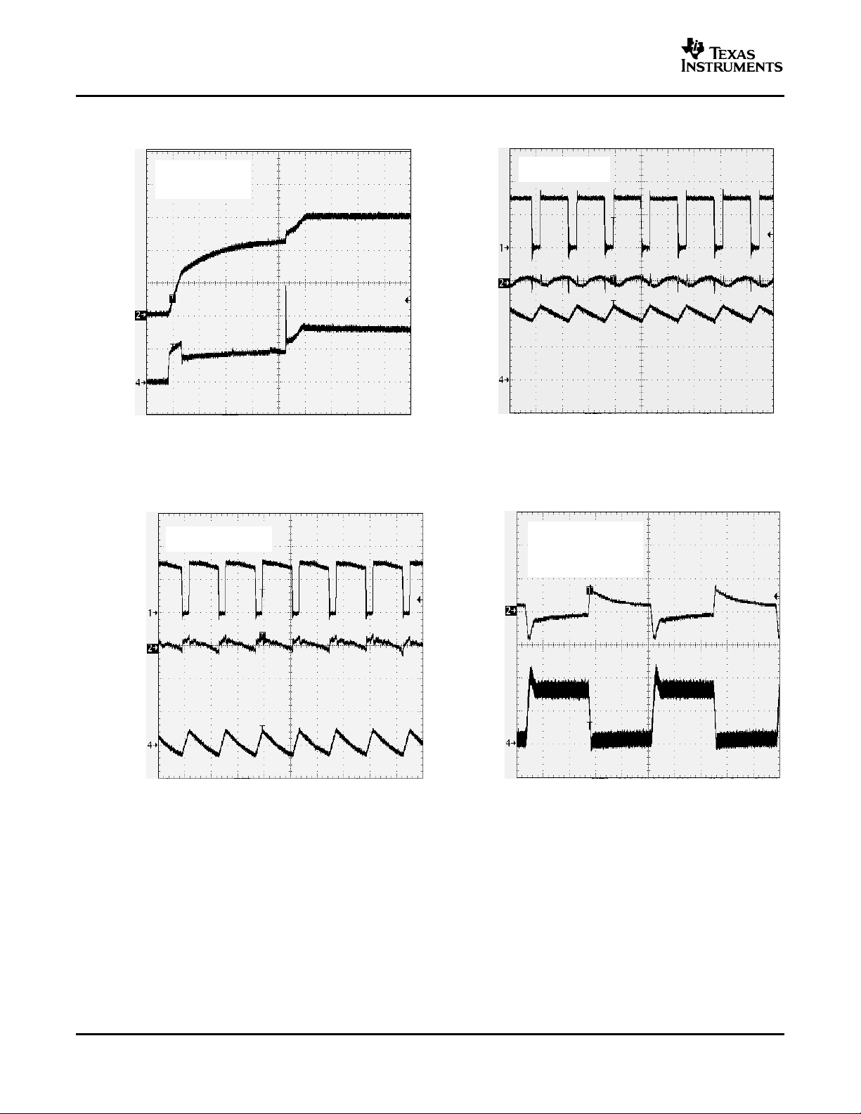
SOFT-START PWM OPERATION BOOST CONVERTER
BOOST CONVERTER CONTINUOUS MODE
Figure 3. Figure 4.
PWM OPERATION BOOST CONVERTER LOAD TRANSIENT RESPONSE BOOST CONVERTER
CONTINUOUS MODE: LIGHT LOAD
Figure 5. Figure 6.
8
Page 9

www.ti.com
0
10
20
30
40
50
60
70
80
90
0 0.5 1 1.5 2
V
I
= 12 V ,
VO = 3.3 V ,
L = 15 H
IO − Output Current − A
Efficiency − %
0
0.05
0.1
0.15
0.2
0.25
−40 −20 0 20 40 60 80 100 120 140
r
DS(on)
− N-Channel Switch −
VI = 8 V ,
VI = 12 V ,
VI = 14 V
TA − Temperature − C
Ω
V
SW
5 V/div
V
O
20 mV/div
I
(Inductor)
100 mA/div
500 ns/div
VI = 12 V,
VO = 3.3 V/45 mA
V
SW
5 V/div
V
O
20 mV/div
I
(Inductor)
1 A/div
500 ns/div
VI = 12 V ,
VO = 3.3 V/1.5 A
TPS65160, TPS65160A
SLVS566B – MARCH 2005 – REVISED JULY 2005
EFFICIENCY STEP-DOWN CONVERTER STEP-DOWN CONVERTER
vs r
LOAD CURRENT vs
Figure 7. Figure 8.
STEP-DOWN CONVERTER STEP-DOWN CONVERTER
PWM OPERATION PWM OPERATION
CONTINUOUS MODE DISCONTINUOUS MODE
- N-CHANNEL SWITCH
DS(ON)
TEMPERATURE
Figure 9. Figure 10.
9
Page 10

www.ti.com
VO1
100 mV/div
I
O
270 mA to 1.3 A
50 s/div
VI = 12 V , V
(logic)
= 3.3 V ,
CO = 2*22 F, FREQ = High
V
O
1 V/div
I
(Inductor)
1 A/div
200 s/div
VI = 12 V ,
VO = 3.3 V/1.2 A
V Logic
2 V/div
VGL
5 V/div
V
S
5 V/div
VGH
10 V/div
2 ms/div
695
700
705
710
715
720
725
730
735
740
−50 0 50 100 150
Switching Frequency − kHz
VI = 8 V ,
VI = 12 V ,
VI = 14 V
TA − Temperature − C
TPS65160, TPS65160A
SLVS566B – MARCH 2005 – REVISED JULY 2005
SOFT-START LOAD TRANSIENT RESPONSE
STEP-DOWN CONVERTER STEP-DOWN CONVERTER
Figure 11. Figure 12.
10
SWITCHING FREQUENCY POWER-UP SEQUENCING
TEMPERATURE
Figure 13. Figure 14.
vs EN2 CONNECTED TO V
IN
Page 11

www.ti.com
V Logic
2 V/div
V
S
5 V/div
VGH
5 V/div
1 ms/div
EN2
2 V/div
TPS65160, TPS65160A
SLVS566B – MARCH 2005 – REVISED JULY 2005
POWER-UP SEQUENCING
EN2 ENABLED SEPARATELY
Figure 15.
11
Page 12

www.ti.com
Current
Control
Soft Start
500 kHz/
750 kHz
Oscillator
D
S
VFB
1.154 V
Comparator
GM Amplifier
Sawtooth
Generator
VFB
1.154
Vref
1.213V
Bias
Vref=1.213 V
Thermal
Shutdown
Sequencing
AVIN SW SW
GND
PGND
PGND
Q1
Negative
Charge Pump
Vref
1.2 13V
OS
GM Amplifier
Low Gain
Current Limit
and
Soft Start
D
S
Q2
I
DLY
Vref
DLY1
OS
OS
AVIN
FREQ
Clock
SUP
DRVP
Q3
Positive
Charge Pump
Current
Control
Soft Start
I
DRVP
COMP
FB
I
DLY
AVIN
Vref
SS
SUP
I
DRVN
SS
SS
D
S
VINB
VINB
Regulator
8 V
Sawtooth
Generator
Compensation
and
Soft Start
Vref
Logic
Clock
Clock/2
Clock/4
0.9 V
0.6 V
Clock Select During Short Circuit
and Soft Start
Control Logic
Ref
Current Limit
SWB
BOOT
FBB
Error Amplifier
SUP
DRVNN
FBN
Vref
1.213V
Reference
Output
VREF
DLY1
Vref
DLY2
DLY2
Step-Down
Converter
Q3
D
S
GD
EN1
EN2
NC
Clock
DLY1
DLY2
Vref
Overvoltage
Comparator
Control Logic
I
DLY
FBP
TPS65160, TPS65160A
SLVS566B – MARCH 2005 – REVISED JULY 2005
BLOCK DIAGRAM
12
Page 13

www.ti.com
TPS65160, TPS65160A
SLVS566B – MARCH 2005 – REVISED JULY 2005
DETAILED DESCRIPTION
Boost Converter
The main boost converter operates in pulse-width modulation (PWM) and at a fixed switching frequency of
500 kHz or 750 kHz set by the FREQ pin. The converter uses an unique fast response, voltage-mode controller
scheme with input voltage feedforward. This achieves excellent line and load regulation (0.03%-A load regulation
typical) and allows the use of small external components. To add higher flexibility to the selection of external
component values, the device uses external loop compensation. Although the boost converter looks like a
nonsynchronous boost converter topology operating in discontinuous conduction mode at light load, the
TPS65160 maintains continuous conduction even at light-load currents. This is achieved with a novel architecture
using an external Schottky diode with an integrated MOSFET in parallel connected between SW and OS. See
the Functional Block Diagram. The intention of this MOSFET is to allow the current to go negative that occurs at
light-load conditions. For this purpose, a small integrated P-Channel MOSFET with typically 10- Ω r
sufficient. When the inductor current is positive, the external Schottky diode with the lower forward voltage
conducts the current. This causes the converter to operate with a fixed frequency in continuous conduction mode
over the entire load current range. This avoids the ringing on the switch pin as seen with standard
nonsynchronous boost converter and allows a simpler compensation for the boost converter.
Soft Start (Boost Converter)
The main boost converter has an adjustable soft start to prevent high inrush current during start-up. The soft-start
time is set by the external capacitor connected to the SS pin. The capacitor connected to the SS pin is charged
with a constant current that increases the voltage on the SS pin. The internal current limit is proportional to the
voltage on the soft-start pin. When the threshold voltage of the internal soft-start comparator is reached, the full
current limit is released. The larger the soft-start capacitor value, the longer the soft-start time.
ds(on)
is
Overvoltage Protection of the Boost Converter
The main boost converter has an overvoltage protection to protect the main switch Q2 at pin (SW) in case the
feedback (FB) pin is floating or shorted to GND. In such an event, the output voltage rises and is monitored with
the overvoltage protection comparator over the OS pin. See the functional block diagram. As soon as the
comparator trips at typically 23 V, TPS65160, (19 V, TPS65160A), the boost converter turns the N-Channel
MOSFET switch off. The output voltage falls below the overvoltage threshold and the converter continues to
operate.
Frequency Select Pin (FREQ)
The frequency select pin (FREQ) allows setting the switching frequency of the entire device to 500 kHz (FREQ =
low) or 750 kHz (FREQ = high). A lower switching frequency gives a higher efficiency with a slightly reduced load
transient regulation.
Thermal Shutdown
A thermal shutdown is implemented to prevent damage caused by excessive heat and power dissipation.
Typically, the thermal shutdown threshold is 155 ° C.
Step-Down Converter
The nonsynchronous step-down converter operates at a fixed switching frequency using a fast response voltage
mode topology with input voltage feedforward. This topology allows simple internal compensation, and it is
designed to operate with ceramic output capacitors. The converter drives an internal 2.6-A N-channel MOSFET
switch. The MOSFET driver is referenced to the switch pin SWB. The N-channel MOSFET requires a gate drive
voltage higher than the switch pin to turn the N-Channel MOSFET on. This is accomplished by a bootstrap gate
drive circuit running of the step-down converter switch pin. When the switch pin SWB is at ground, the bootstrap
capacitor is charged to 8 V. This way, the N-channel gate drive voltage is typically around 8 V.
13
Page 14

www.ti.com
Q3
I
DRVP
DRP
Current
Control
Soft Start
VGHVG
23 V/50 mA
C13
0.47
FBP
Cfly
Vs
R5
R6
F
SUP = Vin for Vs > 15 V
SUP = Vs for Vs 15 V
TPS65160, TPS65160A
SLVS566B – MARCH 2005 – REVISED JULY 2005
DETAILED DESCRIPTION (continued)
Soft Start (Step-Down Converter)
To avoid high inrush current during start-up, an internal soft start is implemented in the TPS65160. When the
step-down converter is enabled over EN1, its reference voltage slowly rises from zero to its power-good
threshold of typically 90% of Vref. When the reference voltage reaches this power-good threshold, the error
amplifier is released to its normal operation at its normal duty cycle. To further limit the inrush current during soft
start, the converter frequency is set to 1/4
comparator that monitors the feedback voltage. See the internal block diagram. Soft start is typically completed
within 1 ms.
Short-Circuit Protection (Step-Down Converter)
To limit the short-circuit current, the device has a cycle-by-cycle current limit. To avoid the short-circuit current
rising above the internal current limit when the output is shorted to GND, the switching frequency is reduced as
well. This is implemented by two comparators monitoring the feedback voltage. The step-down converter
switching frequency is reduced to 1/2 of fs when the feedback is below 0.9 V and to 1/4
frequency when the feedback voltage is below 0.6 V.
Positive Charge Pump
The positive charge pump provides a regulated output voltage set by the external resistor divider. Figure 16
shows an extract of the positive charge-pump driver circuit. The maximum voltage which can be applied to the
charge-pump driver supply pin, SUP, is 15 V. For applications where the boost converter voltage Vs is higher
than 15 V, the SUP pin needs to be connected to the input. The operation of the charge-pump driver can be
understood best with Figure 16 . During the first cycle, Q3 is turned on and the flying capacitor Cfly charges to the
source voltage, Vs. During the next clock cycle, Q3 is turned off and the current source charges the drive pin,
DRP, up to the supply voltage, VSUP. Because the flying capacitor voltage sits on top of the drive pin voltage,
the maximum output voltage is Vsup+Vs.
th
of the switching frequency fs and then 1/2 of fs determined by the
th
of the switching
Figure 16. Extract of the Positive Charge-Pump Driver
If higher output voltages are required, another charge-pump stage can be added to the output.
Setting the output voltage:
14
Page 15

www.ti.com
V
out
1.2131
R5
R6
R5 R6
V
out
V
FB
1
R6
V
out
1.213
1
V
out
V
REF
R3
R4
1.213 V
R3
R4
R3 R4
|V
out
|
V
REF
R4
|V
out
|
1.213
EN2
EN1
GD
Vo4
VGL
DLY1
Vs
VGH
DLY2
Vin
VinVs, VGH
Fall Time Depends on Load
Current and Feedback Resistor
TPS65160, TPS65160A
SLVS566B – MARCH 2005 – REVISED JULY 2005
DETAILED DESCRIPTION (continued)
Negative Charge Pump
The negative charge pump provides a regulated output voltage set by the external resistor divider. The negative
charge pump operates similar to the positive charge pump with the difference that the voltage on the supply pin,
SUP, is inverted. The maximum negative output voltage is VGL = (–V
across the external diodes and internal charge-pump MOSFETs. In case VGL needs to be lower than –VS, an
additional charge-pump stage needs to be added.
Setting the output voltage:
)+Vdrop. Vdrop is the voltage drop
SUP
The lower feedback resistor value, R4, should be in a range between 40 k Ω to 120 k Ω or the overall feedback
resistance should be within 500 k Ω to 1 M Ω . Smaller values load the reference too heavily, and larger values
may cause stability problems. The negative charge pump requires two external Schottky diodes. The peak
current rating of the Schottky diode has to be twice the load current of the output. For a 20-mA output current,
the dual-Schottky diode BAT54 is a good choice.
Power-On Sequencing (EN1, EN2, DLY1, DLY2)
The TPS65160 has an adjustable power-on sequencing set by the capacitors connected to DLY1 and DLY2 and
controlled by EN1 and EN2. Pulling EN1 high enables the step-down converter and then the negative
charge-pump driver. DLY1 sets the delay time between the step-down converter and negative charge-pump
driver. EN2 enables the boost converter and positive charge-pump driver at the same time. DLY2 sets the delay
time between the step-down converter Vlogic and the boost converter Vs. This is especially useful to adjust the
delay when EN2 is always connected to Vin. If EN2 goes high after the step-down converter is already enabled,
then the delay DLY2 starts when EN2 goes high. See Figure 17 and Figure 18 .
Figure 17. Power-On Sequencing With EN2 Always High (EN2=Vin)
15
Page 16

www.ti.com
EN2
EN1
GD
Vo4
VGL
DLY1
Vs
VGH ,Vs
DLY2
Vin
VGH
Vin
Fall Time Depends on Load
Current and Feedback Resistor
C
dly
4.8 A td
Vref
4.8 A td
1.213 V
with td Desired delay time
C
dly
4.8 A 2.3 ms
1.213 V
9.4 nF Cdly 10 nF
TPS65160, TPS65160A
SLVS566B – MARCH 2005 – REVISED JULY 2005
DETAILED DESCRIPTION (continued)
Figure 18. Power-On Sequencing Using EN1 and EN2
Setting the Delay Times DLY1, DLY2
Connecting an external capacitor to the DLY1 and DLY2 pins sets the delay time. If no delay time is required,
these pins can be left open. To set the delay time, the external capacitor connected to DLY1 and DLY2 is
charged with a constant current source of typically 4.8 µA. The delay time is terminated when the capacitor
voltage has reached the internal reference voltage of Vref = 1.213 V. The external delay capacitor is calculated:
Example for setting a delay time of 2.3 mS:
Gate Drive Pin (GD)
This is an open-drain output that goes low when the boost converter, Vs, is within regulation. The gate drive pin
GD remains low until the input voltage or enable EN2 is cycled to ground.
Undervoltage Lockout
To avoid misoperation of the device at low input voltages, an undervoltage lockout is included which shuts down
the device at voltages lower than 6 V.
Input Capacitor Selection
For good input voltage filtering, low ESR ceramic capacitors are recommended. The TPS65160 has an analog
input, AVIN, and two input pins for the buck converter VINB. A 1-µF input capacitor should be connected directly
from the AVIN to GND. Two 22-µF ceramic capacitors are connected in parallel from the buck converter input
VINB to GND. For better input voltage filtering, the input capacitor values can be increased. See Table 1 and the
Application Information section for input capacitor recommendations.
16
Page 17

www.ti.com
D 1
Vin
Vout
I
avg
(
1 D) lsw
Vin
Vout
2.8 A with lsw minimum switch current of the TPS65160 (2.8 A).
I
swpeak
Vin D
2 ƒs L
I
out
1 D
TPS65160, TPS65160A
SLVS566B – MARCH 2005 – REVISED JULY 2005
DETAILED DESCRIPTION (continued)
Table 1. Input Capacitor Selection
CAPACITOR VOLTAGE RATING COMPONENT SUPPLIER COMMENTS
22 µF/1210 16 V Taiyo Yuden EMK325BY226MM C
1 µF/1206 16 V Taiyo Yuden EMK316BJ106KL C
Boost Converter Design Procedure
The first step in the design procedure is to verify whether the maximum possible output current of the boost
converter supports the specific application requirements. A simple approach is to use the converter efficiency, by
taking the efficiency numbers from the provided efficiency curves or to use a worst-case assumption for the
expected efficiency, e.g., 80%.
1. Duty Cycle:
2. Maximum output current:
3. Peak switch current:
(VINB)
IN
(AVIN)
IN
With
Isw = converter switch current (minimum switch current limit = 2.8 A)
fs = converter switching frequency (typical 500 kHz/750 kHz)
L = Selected inductor value
η = Estimated converter efficiency (use the number from the efficiency curves or 0.8 as an estimation)
The peak switch current is the steady-state peak switch current that the integrated switch, inductor, and external
Schottky diode must be able to handle. The calculation must be done for the minimum input voltage where the
peak switch current is highest.
Inductor Selection (Boost Converter)
The TPS65160 operates typically with a 10-µH inductor. Other possible inductor values are 6.8-µH or 22-µH. The
main parameter for the inductor selection is the saturation current of the inductor, which should be higher than
the peak switch current as previously calculated, with additional margin to cover for heavy load transients. The
alternative, more conservative approach, is to choose the inductor with saturation current at least as high as the
typical switch current limit of 3.5 A. The second important parameter is the inductor DC resistance. Usually, the
lower the DC resistance the higher the efficiency. The efficiency difference between different inductors can vary
between 2% to 10%. Possible inductors are shown in Table 2 .
Table 2. Inductor Selection (Boost Converter)
INDUCTOR VALUE COMPONENT SUPPLIER DIMENSIONS in mm Isat/DCR
22 µH Coilcraft MSS1038-103NX 10,2 x 10,2 x 3,6 2.9 A/73 m Ω
22 µH Coilcraft DO3316-103 12,85 x 9,4 x 5,21 3.8 A/38 m Ω
10 µH Sumida CDRH8D43-100 8,3 x 8,3 x 4,5 4.0 A/29 m Ω
10 µH Sumida CDH74-100 7,3 x 8,0 x 5,2 2.75 A/43 m Ω
10 µH Coilcraft MSS1038-103NX 10,2 x 10,2 x 3,6 4.4 A/35 m Ω
6.8 µH Wuerth Elektronik 7447789006 7,3 x 7,3 x 3,2 2.5 A/44 m Ω
17
Page 18

www.ti.com
D 1
Vout
Vin
I
avg
(
1 D) lsw
Vin
Vout
2.8 A with lsw minimum switch current of the TPS65160 (2.8 A).
V
out
1.146 V 1
R1
R2
Cƒƒ
1
2 ƒz R1
1
2 10 kHz R1
TPS65160, TPS65160A
SLVS566B – MARCH 2005 – REVISED JULY 2005
Output Capacitor Selection (Boost Converter)
For best output voltage filtering, a low ESR output capacitor is recommended. Ceramic capacitors have a low
ESR value and work best with the TPS65160. Usually, three 22-µF ceramic output capacitors in parallel are
sufficient for most applications. If a lower voltage drop during load transients is required, more output
capacitance can be added. See Table 3 for the selection of the output capacitor.
Table 3. Output Capacitor Selection (Boost Converter)
CAPACITOR VOLTAGE RATING COMPONENT SUPPLIER
22 µF/1812 16 V Taiyo Yuden EMK432BJ226MM
Rectifier Diode Selection (Boost Converter)
To achieve high efficiency, a Schottky diode should be used. The reverse voltage rating should be higher than
the maximum output voltage of the converter. The average rectified forward-current rating needed for the
Schottky diode is calculated as the off-time of the converter times the maximum switch current of the TPS65160:
Usually, a Schottky diode with 2-A maximum average rectified forward-current rating is sufficient for most
applications. Secondly, the Schottky rectifier has to be able to dissipate the power. The dissipated power is the
average rectified forward current times the diode forward voltage.
P
= I
x V
D
avg
= Isw x (1 x D) x V
F
(with Isw = minimum switch current of the TPS65160 (2.6 A)
F
Table 4. Rectifier Diode Selection (Boost Converter)
CURRENT RATING Vr V
I
avg
3 A 20 V 0.36 at 3 A 46 ° C/W SMC MBRS320, International Rectifier
2 A 20 V 0.44 V at 3 A 75 ° C/W SMB SL22, Vishay Semiconductor
2 A 20 V 0.5 at 2 A 75 ° C/W SMB SS22, Fairchild Semiconductor
forward
R θ
JA
SIZE COMPONENT SUPPLIER
Setting the Output Voltage and Selecting the Feedforward Capacitor (Boost Converter)
The output voltage is set by the external resistor divider and is calculated as:
Across the upper resistor, a bypass capacitor is required to achieve a good load transients response and to have
a stable converter loop. Together with R1, the bypass capacitor Cff sets a zero in the control loop. Depending on
the inductor value, the zero frequency needs to be set. For a 6.8-µH or 10-µH inductor, fz = 10 kHz and for a
22-µH inductor, fz = 7 kHz.
A value coming closest to the calculated value should be used.
Compensation (COMP) (Boost Converter)
The regulator loop can be compensated by adjusting the external components connected to the COMP pin. The
COMP pin is the output of the internal transconductance error amplifier. A single capacitor connected to this pin
sets the low-frequency gain. Usually, a 22-nF capacitor is sufficient for most of the applications. Adding a series
resistor sets an additional zero and increases the high-frequency gain. The following formula calculates at what
frequency the resistor increases the high-frequency gain.
18
Page 19

www.ti.com
ƒ
z
1
2 Cc Rc
V
out
1.213 V 1
R1
R2
C
z
1
2 8 kHz R1
1
2 8 kHz 2k
9.9 nF 10 nF
(Example for the 3.3-V output)
IL Vout
1
Vout
Vin
L ƒ
I
Lmax
I
outmax
I
L
2
TPS65160, TPS65160A
SLVS566B – MARCH 2005 – REVISED JULY 2005
Lower input voltages require a higher gain and therefore a lower compensation capacitor value.
Step-Down Converter Design Procedure
Setting the Output Voltage
The step-down converter uses an external voltage divider to set the output voltage. The output voltage is
calculated as:
with R1 as 1.2 k Ω , and internal reference voltage V(ref)typ = 1.213 V
At load current <1 mA, the device operates in discontinuous conduction mode. When the load current is reduced
to zero, the output voltage rises slightly above the nominal output voltage. At zero load current, the device skips
clock cycles but does not completely stop switching; thus, the output voltage sits slightly higher than the nominal
output voltage. Therefore, the lower feedback resistor is selected to be around 1.2 k Ω to always have around
1-mA minimum load current.
Selecting the Feedforward Capacitor
The feedforward capacitor across the upper feedback resistor divider sets a zero in the converter loop transfer
function. For a 15-µH inductor, fz = 8 kHz and when a 22-µH inductor is used, fz = 17 kHz.
Usually a capacitor value closest to the calculated value is selected.
Inductor Selection (Step-Down Converter)
The TPS65160 operates typically with a 15-µH inductor value. For high efficiencies the inductor should have a
low DC resistance to minimize conduction losses. This needs to be considered when selecting the appropriate
inductor. In order to avoid saturation of the inductor, the inductor should be rated at least for the maximum output
current of the converter, plus the inductor ripple current that is calculated as:
With:
f = Switching frequency (750 kHz, 500 kHz minimal)
L = Inductor value (typically 15 µH)
∆ IL= Peak-to-peak inductor ripple current
I
= Maximum inductor current
Lmax
The highest inductor current occurs at maximum Vin. A more conservative approach is to select the inductor
current rating just for the typical switch current of 2.6 A.
Table 5. Inductor Selection (Step-Down Converter)
INDUCTOR VALUE COMPONENT SUPPLIER DIMENSIONS in mm Isat/DCR
15 µH Sumida CDRH8D28-150 8,3 x 8,3 x 3,0 1.9 A/53 m Ω
15 µH Coilcraft MSS1038-153NX 10,2 x 10,2 x 3,6 3.6 A/50 m Ω
15 µH Wuerth 7447789115 7,3 x 7,3 x 3,2 1.75 A/100 m Ω
19
Page 20

www.ti.com
D 1
Vout
Vin
I
avg
(1 D) Isw 1
Vout
Vin
2 A with Isw minimum switch current of the TPS65160 (2 A)
TPS65160, TPS65160A
SLVS566B – MARCH 2005 – REVISED JULY 2005
Rectifier Diode Selection (Step-Down Converter)
To achieve high efficiency, a Schottky diode should be used. The reverse voltage rating should be higher than
the maximum output voltage of the step-down converter. The averaged rectified forward current at which the
Schottky diode needs to be rated is calculated as the off-time of the step-down converter times the maximum
switch current of the TPS65160:
Usually, a Schottky diode with 1.5-A or 2-A maximum average rectified forward current rating is sufficient for
most applications. Secondly, the Schottky rectifier has to be able to dissipate the power. The dissipated power is
the average rectified forward current times the diode forward voltage.
P
= I
x V
D
avg
CURRENT RATING Vr V
= Isw x (1 – D) x VFwith Isw = minimum switch current of the TPS65160 (2 A).
F
Table 6. Rectifier Diode Selection (Step-Down Converter)
I
avg
3 A 20 V 0.36 V at 3 A 46 ° C/W SMC MBRS320, International Rectifier
2 A 20 V 0.44 V at 2 A 75 ° C/W SMB SL22, Vishay Semiconductor
2 A 20 V 0.5 V at 2 A 75 ° C/W SMB SS22, Fairchild Semiconductor
1.5 A 20 V 0.445 V at 1.0 A 88 ° C/W SMA SL12, Vishay Semiconductor
forward
R θ
JA
SIZE COMPONENT SUPPLIER
Output Capacitor Selection (Step-Down Converter)
The device is designed to work with ceramic output capacitors. When using a 15-µH inductor, two 22-µF ceramic
output capacitors are recommended. More capacitance can be added to improve the load transient response.
Table 7. Output Selection (Boost Converter)
CAPACITOR VOLTAGE RATING COMPONENT SUPPLIER
22 µF/0805 6.3 V Taiyo Yuden JMK212BJ226MG
Layout Consideration
The PCB layout is an important step in the power supply design. An incorrect layout could cause converter
instability, load regulation problems, noise, and EMI issues. Especially with a switching dc-dc converter at high
load currents, too-thin PCB traces can cause significant voltage spikes. Good grounding becomes important as
well. If possible, a common ground plane to minimize ground shifts between analog (GND) and power ground
(PGND) is recommended. Additionally, the following PCB design layout guidelines are recommended for the
TPS65160:
1. Separate the power supply traces for AVIN and VINB, and use separate bypass capacitors.
2. Use a short and wide trace to connect the OS pin to the output of the boost converter.
3. To minimize noise coupling into the OS pin, use a 470-pF bypass capacitor to GND.
4. Use short traces for the charge-pump drive pins (DRN, DRP) of VGH and VGL because these traces carry
switching waveforms.
5. Place the flying capacitors as close as possible to the DRP and DRN pin, avoiding a high voltage spike at
these pins.
6. Place the Schottky diodes as close as possible to the IC, respective to the flying capacitors connected to the
DRP and DRN.
7. Route the feedback network of the negative charge pump away from the drive pin traces (DRN) of the
negative charge pump. This avoids parasitic coupling into the feedback network of the negative charge pump
giving good output voltage accuracy and load ragulation. To do this, use the FREQ pin and trace to isolate
DRN from FBN.
20
Page 21

www.ti.com
COMP
VINB
FREQ
EN1
EN2
DRN
FBN
REF
PGND
PGND
SW
SW
AVIN
FB
GND
OS
DRP
FBP
Boot
SWB
NC
DLY1
TPS65160
D1
SL22
D2
D3
D4
D5
SS
VINB
GD
FBB
DLY2
SUP
GD
Vin
12 V
C1
2*22 F
C3
1 F
C16
1 F
C6
0.47 F
VGL
−5 V/50 mA
C7
470 F
R3
620 k
R4
150 k
C8
220 nF
C9
22 nF
C10
10 nF
C11
10 nF
C17
22 nF
D6
SL22
L2
15 H
Cb
100 nF
R8
1.2 k
R7
2 k
C14
10 nF
C12
2*22 F
Vlogic
3.3 V/1.5 A
R6
44.2 k
R5
909 k
C13
0.47 F
VGH
26 V/50 mA
0.47 FC5
Vs
15 V/1.5 A
R2
56 k
C15
470 nF
C2
3*22 F
R1
680 k
C4
22 pF
L1
10 H
8
12
20
21
22
16
9
11
13
24
6
7
28
25
4
5
1
3
23
27
10
14
17
18
19
15
2
26
TPS65160, TPS65160A
SLVS566B – MARCH 2005 – REVISED JULY 2005
APPLICATION INFORMATION
Figure 19. Positive-Charge Pump Doubler Running From the Output V
Required When Higher VGH Voltages Are Needed.
S
(SUP = VS)
21
Page 22

www.ti.com
C3
1 F
C6
0.47 F
VGL
−5 V/50 mA
C7
470 F
R3
620 k
R4
150 k
C8
220 nF
C9
22 nF
C10
10 nF
C11
10 nF
C17
22 nF
D6
SL22
L2
15 H
Cb
100 nF
R8
1.2 k
R7
2 k
C14
10 nF
C13
0.47 F
Vlogic
3.3 V/1.5 A
R6
56 k
R5
1 M
VGH
23 V/50 mA
0.47 FC5
Vs
15 V/1.5 A
R2
56 k
C15
470 nF
C2
3*22 F
R1
680 k
C4
22 pF
L1
10 H
Vin
12 V
C1
2*22 F
C16
1 F
COMP
VINB
FREQ
EN1
EN2
DRN
FBN
REF
PGND
PGND
SW
SW
AVIN
FB
GND
OS
DRP
FBP
Boot
SWB
NC
DLY1
TPS65160
D1
SL22
D2
D3
D4
D5
SS
VINB
GD
FBB
DLY2
SUP
GD
GD
SI2343
C18
220 nF
R9
510 k
R10
100 k
C19
1 F
C12
2*22 F
8
12
20
21
22
16
9
11
13
24
6
7
28
25
4
5
1
3
23
27
10
14
17
18
19
15
2
26
TPS65160, TPS65160A
SLVS566B – MARCH 2005 – REVISED JULY 2005
APPLICATION INFORMATION (continued)
Figure 20. Driving an Isolation FET for V
22
using the GD Pin
S
Page 23

www.ti.com
C3
1 F
C6
0.47 F
VGL
−5 V/50 mA
C7
470 F
R3
620 k
R4
150 k
C8
220 nF
C9
22 nF
C10
10 nF
C17
22 nF
D6
SL22
L2
15 H
Cb
100 nF
R8
1.2 k
R7
2 k
C14
10 nF
C12
2*22 F
Vlogic
3.3 V/1.5 A
R6
76 k
R5
1 M
VGH
23 V/50 mA
0.47 FC5
Vs
13.5 V/2 A
C15
470 nF
C2
3*22 F
R1
820 k
C4
22 pF
L1
6.9 H
Vin
12 V 10%
C1
2*22 F
COMP
VINB
FREQ
EN1
EN2
DRN
FBN
REF
PGND
PGND
SW
SW
AVIN
FB
GND
OS
DRP
FBP
Boot
SWB
NC
DLY1
TPS65160
D1
SL22
D2
D3
D4
D5
SS
VINB
GD
FBB
DLY2
SUP
GD
C16
1 F
C11
10 nF
R2
75 k
C13
0.47 F
8
12
20
21
22
16
9
11
13
24
6
7
28
25
4
5
1
3
23
27
10
14
17
18
19
15
2
26
APPLICATION INFORMATION (continued)
TPS65160, TPS65160A
SLVS566B – MARCH 2005 – REVISED JULY 2005
Figure 21. 12-V to 13.5-V Conversion
23
Page 24

PACKAGE OPTION ADDENDUM
www.ti.com
26-Jun-2006
PACKAGING INFORMATION
Orderable Device Status
(1)
Package
Type
Package
Drawing
Pins Package
Qty
Eco Plan
TPS65160APWP ACTIVE HTSSOP PWP 28 50 Green (RoHS &
no Sb/Br)
TPS65160APWPG4 ACTIVE HTSSOP PWP 28 50 Green (RoHS &
no Sb/Br)
TPS65160APWPR ACTIVE HTSSOP PWP 28 2000 Green (RoHS &
no Sb/Br)
TPS65160APWPRG4 ACTIVE HTSSOP PWP 28 2000 Green (RoHS &
no Sb/Br)
TPS65160PWP ACTIVE HTSSOP PWP 28 50 Green (RoHS &
no Sb/Br)
TPS65160PWPG4 ACTIVE HTSSOP PWP 28 50 Green (RoHS &
no Sb/Br)
TPS65160PWPR ACTIVE HTSSOP PWP 28 2000 Green (RoHS &
no Sb/Br)
TPS65160PWPRG4 ACTIVE HTSSOP PWP 28 2000 Green (RoHS &
no Sb/Br)
(1)
The marketing status values are defined as follows:
ACTIVE: Product device recommended for new designs.
LIFEBUY: TI has announced that the device will be discontinued, and a lifetime-buy period is in effect.
NRND: Not recommended for new designs. Device is in production to support existing customers, but TI does not recommend using this part in
a new design.
PREVIEW: Device has been announced but is not in production. Samples may or may not be available.
OBSOLETE: TI has discontinued the production of the device.
(2)
Lead/Ball Finish MSL Peak Temp
CU NIPDAU Level-2-260C-1 YEAR
CU NIPDAU Level-2-260C-1 YEAR
CU NIPDAU Level-2-260C-1 YEAR
CU NIPDAU Level-2-260C-1 YEAR
CU NIPDAU Level-2-260C-1 YEAR
CU NIPDAU Level-2-260C-1 YEAR
CU NIPDAU Level-2-260C-1 YEAR
CU NIPDAU Level-2-260C-1 YEAR
(3)
(2)
Eco Plan - The planned eco-friendly classification: Pb-Free (RoHS), Pb-Free (RoHS Exempt), or Green (RoHS & no Sb/Br) - please check
http://www.ti.com/productcontent for the latest availability information and additional product content details.
TBD: The Pb-Free/Green conversion plan has not been defined.
Pb-Free (RoHS): TI's terms "Lead-Free" or "Pb-Free" mean semiconductor products that are compatible with the current RoHS requirements
for all 6 substances, including the requirement that lead not exceed 0.1% by weight in homogeneous materials. Where designed to be soldered
at high temperatures, TI Pb-Free products are suitable for use in specified lead-free processes.
Pb-Free (RoHS Exempt): This component has a RoHS exemption for either 1) lead-based flip-chip solder bumps used between the die and
package, or 2) lead-based die adhesive used between the die and leadframe. The component is otherwise considered Pb-Free (RoHS
compatible) as defined above.
Green (RoHS & no Sb/Br): TI defines "Green" to mean Pb-Free (RoHS compatible), and free of Bromine (Br) and Antimony (Sb) based flame
retardants (Br or Sb do not exceed 0.1% by weight in homogeneous material)
(3)
MSL, Peak Temp. -- The Moisture Sensitivity Level rating according to the JEDEC industry standard classifications, and peak solder
temperature.
Important Information and Disclaimer:The information provided on this page represents TI's knowledge and belief as of the date that it is
provided. TI bases its knowledge and belief on information provided by third parties, and makes no representation or warranty as to the
accuracy of such information. Efforts are underway to better integrate information from third parties. TI has taken and continues to take
reasonable steps to provide representative and accurate information but may not have conducted destructive testing or chemical analysis on
incoming materials and chemicals. TI and TI suppliers consider certain information to be proprietary, and thus CAS numbers and other limited
information may not be available for release.
In no event shall TI's liability arising out of such information exceed the total purchase price of the TI part(s) at issue in this document sold by TI
to Customer on an annual basis.
Addendum-Page 1
Page 25

Page 26

Page 27

Page 28

IMPORTANT NOTICE
Texas Instruments Incorporated and its subsidiaries (TI) reserve the right to make corrections, modifications,
enhancements, improvements, and other changes to its products and services at any time and to discontinue
any product or service without notice. Customers should obtain the latest relevant information before placing
orders and should verify that such information is current and complete. All products are sold subject to TI’s terms
and conditions of sale supplied at the time of order acknowledgment.
TI warrants performance of its hardware products to the specifications applicable at the time of sale in
accordance with TI’s standard warranty. Testing and other quality control techniques are used to the extent TI
deems necessary to support this warranty . Except where mandated by government requirements, testing of all
parameters of each product is not necessarily performed.
TI assumes no liability for applications assistance or customer product design. Customers are responsible for
their products and applications using TI components. To minimize the risks associated with customer products
and applications, customers should provide adequate design and operating safeguards.
TI does not warrant or represent that any license, either express or implied, is granted under any TI patent right,
copyright, mask work right, or other TI intellectual property right relating to any combination, machine, or process
in which TI products or services are used. Information published by TI regarding third-party products or services
does not constitute a license from TI to use such products or services or a warranty or endorsement thereof.
Use of such information may require a license from a third party under the patents or other intellectual property
of the third party, or a license from TI under the patents or other intellectual property of TI.
Reproduction of information in TI data books or data sheets is permissible only if reproduction is without
alteration and is accompanied by all associated warranties, conditions, limitations, and notices. Reproduction
of this information with alteration is an unfair and deceptive business practice. TI is not responsible or liable for
such altered documentation.
Resale of TI products or services with statements different from or beyond the parameters stated by TI for that
product or service voids all express and any implied warranties for the associated TI product or service and
is an unfair and deceptive business practice. TI is not responsible or liable for any such statements.
Following are URLs where you can obtain information on other Texas Instruments products and application
solutions:
Products Applications
Amplifiers amplifier.ti.com Audio www.ti.com/audio
Data Converters dataconverter.ti.com Automotive www.ti.com/automotive
DSP dsp.ti.com Broadband www.ti.com/broadband
Interface interface.ti.com Digital Control www.ti.com/digitalcontrol
Logic logic.ti.com Military www.ti.com/military
Power Mgmt power.ti.com Optical Networking www.ti.com/opticalnetwork
Microcontrollers microcontroller.ti.com Security www.ti.com/security
Low Power Wireless www.ti.com/lpw Telephony www.ti.com/telephony
Video & Imaging www.ti.com/video
Wireless www.ti.com/wireless
Mailing Address: Texas Instruments
Post Office Box 655303 Dallas, Texas 75265
Copyright 2006, Texas Instruments Incorporated
 Loading...