

www.ti.com
VIN
DRVN
FBN
REF
COMP
DLY1
DLY2
FDLY
SW SW
SUP
DRVP
GD
CPI
FBP
GND
PGND
PGND
VCOM
TPS65150
ADJ
CTRL
VGH
FB
IN
Vin
5 V
R8
500 k
C6
1 nF
R7
500 k
L1
3.9 H
D1
C1
22 F
C7
0.33 FD2
R3
620 k
D3
C3
0.33 F
R4
150 k
C8
220 nF
VGH
Control Signal
C9
2.2 nF
C10
22 pF
C11
10 nF
C12
10 nF
C13
100 nF
CPI
C16
0.33 F
D4
C5
1 F
C4
0.33 F
VGH
23 V/20 mA
V
COM
Output
C14
1 F
C15
22 pF
R1
820 k
R2
75 k
C2
22 F
R6
56 k
R5
1 M
CPI
V
S
13.5 V/450 mA
D5
VGL
−5 V/20 mA
V
IN
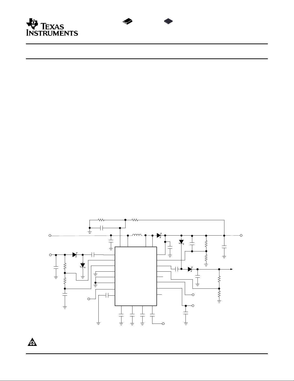
Low Input Voltage, Compact LCD Bias IC With VCOM Buffer
FEATURES APPLICATIONS
• 1.8-V to 6-V Input Voltage Range
• Integrated VCOM Buffer
• High Voltage Switch to Isolate VGH
• Gate Voltage Shaping of VGH
• 2-A Internal MOSFET Switch
• Main Output Vs up to 15 V With <1% Output
Voltage Accuracy
• Virtual Synchronous Converter Technology
• Negative Regulated Charge Pump Driver VGL
• Positive Regulated Charge Pump Driver VGH
• Adjustable Power On Sequencing
• Adjustable Fault Detection Timing
• Gate Drive Signal for external isolation
MOSFET
• Thermal Shutdown
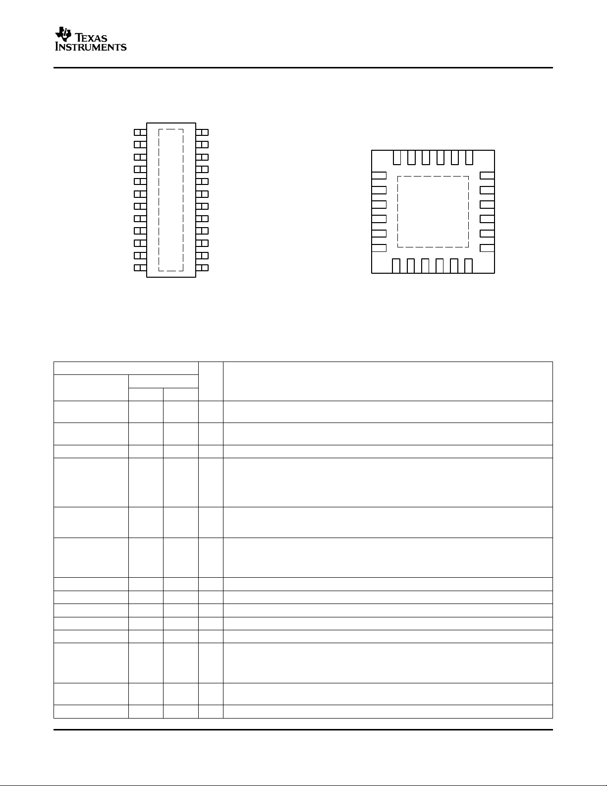
• Available in TSSOP-24 Package
• Available in QFN-24 Package
TPS65150
SLVS576 – SEPTEMBER 2005
• TFT LCD Displays for Notebooks
• TFT LCD Display for Monitor
• Car Navigation Display
DESCRIPTION
The TPS65150 offers a very compact and small
power supply solution that provides all three voltages
required by thin film transistor (TFT) LCD displays.
With an input voltage range of 1.8 V to 6.0 V the
device is ideal for notebooks powered by a 2.5-V or
3.3-V input rail or monitor applications with a 5-V input voltage rail. Additionally the TPS65150 provides an integrated high current buffer to provide the VCOM voltage for the TFT backplane.
Two regulated adjustable charge pump driver provide
the positive VGH and negative VGL bias voltages for
the TFT. The device incorporates adjustable power
on sequencing for VGL as well as for VGH. This
avoids any additional external components to
implement application specific sequencing. The
device has an integrated high voltage switch to
isolate VGH.
TYPICAL APPLICATION
Please be aware that an important notice concerning availability, standard warranty, and use in critical applications of Texas
Instruments semiconductor products and disclaimers thereto appears at the end of this data sheet.
PowerPad is a trademark of Texas Instruments.
PRODUCTION DATA information is current as of publication date.
Products conform to specifications per the terms of the Texas
Instruments standard warranty. Production processing does not
necessarily include testing of all parameters.
Copyright © 2005, Texas Instruments Incorporated
www.ti.com
TPS65150
SLVS576 – SEPTEMBER 2005
These devices have limited built-in ESD protection. The leads should be shorted together or the device
placed in conductive foam during storage or handling to prevent electrostatic damage to the MOS gates.
DESCRIPTION (CONTINUED)
The same internal circuit can also be used to provide a gate shaping signal of VGH for the LCD panel controlled
by the signal applied to the CTRL input. For highest safety the TPS65150 has an integrated adjustable shutdown
latch feature to allow application specific flexibility. The device monitors the outputs (Vs, VGL, VGH); and, as
soon as one of the outputs falls below its power good threshold, the device enters shutdown latch, after its
adjustable delay time has passed by.
ORDERING INFORMATION
T
A
–40 ° C to 85 ° C
(1) For the most current package and ordering information, see the Package Option Addendum at the end of this document, or see the TI
Web site at www.ti.com .
(2) The PWP package is available taped and reeled. Add R suffix to the device type (TPS65150PWPR) to order quantities of 2000 and
(TPS65150RGER) to order quantities of 3000 devices per reel. Without suffix the device is shipped in tubes.
ORDERING NUMBER PACKAGE
TPS65150PWP TSSOP24 (PWP) TPS65150
TPS65150RGE QFN-24 (RGE) TPS65150
(1)
(2)
PACKAGE MARKING
ABSOLUTE MAXIMUM RATINGS
over operating free-air temperature range (unless otherwise noted)
Voltages on pin VIN
Voltages on pin SUP –0.3 V to 15.5 V
Voltage on pin SW 20 V
Voltage on CTRL –0.3 V to 7 V
Voltage on GD 15.5 V
Voltage on CPI 32V
Continuous power dissipation See Dissipation Rating Table
Operating junction temperature range –40 ° C to 150 ° C
Storage temperature range –65 ° C to 150 ° C
Lead temperature (soldering, 10 sec) 260 ° C
(1) Stresses beyond those listed under absolute maximum ratings may cause permanent damage to the device. These are stress ratings
only, and functional operation of the device at these or any other conditions beyond those indicated under recommended operating
conditions is not implied. Exposure to absolute-maximum-rated conditions for extended periods may affect device reliability.
(2) All voltage values are with respect to network ground terminal.
(2)
(1)
UNIT
–0.3 V to 7 V
DISSIPATION RATINGS
PACKAGE θ
24 pin TSSOP 30.13 C ° /W ( PowerPad™ 3.3 W 1.83 W 1.32 W
24 pin QFN 30 C ° /W (PowerPad
JA
soldered)
TM
soldered) 3.3 W 1.8 W 1.3 W
TA≤ 25 ° C TA= 70 ° C TA= 85 ° C
POWER RATING POWER RATING POWER RATING
RECOMMENDED OPERATING CONDITIONS
MIN TYP MAX UNIT
VIN Input voltage range 1.8 6.0 V
V
L Inductor
T
(1) Refer to application section for further information.
2
Output voltage range of the main boost converter V
S
A
(1)
Operating ambient temperature –40 85 ° C
S
15 V
4.7 µH
www.ti.com
TPS65150
SLVS576 – SEPTEMBER 2005
RECOMMENDED OPERATING CONDITIONS (continued)
MIN TYP MAX UNIT
T
ELECTRICAL CHARACTERISTICS
VIN = 3.3 V, Vs = 10 V, TA= –40 ° C to 85 ° C, typical values are at TA= 25 ° C (unless otherwise noted)
SUPPLY CURRENT
V
I
QVIN
I
QSUP
I
QVCOM
V
V
LOGIC SIGNALS CTRL
V
V
I
I
MAIN BOOST CONVERTER
V
V
I
FB
R
I
MAX
I
LIM
Ileak Switch leakage current V
Vovp Output overvoltage protection V
f
OSC
NEGATIVE CHARGE PUMP VGL
VGL Output voltage range –2 V
V
V
I
FB
R
V
POSITIVE CHARGE PUMP OUTPUT
V
Operating junction temperature –40 125 ° C
J
PARAMETER TEST CONDITIONS MIN TYP MAX UNIT
IN
Input voltage range 1.8 6.0 V
No load quiescent current into Vin Device is not switching 14 25 µA
No load quiescent current into SUP Device is not switching 1.9 3 mA
VCOM quiescent current into SUP 750 1500 µA
UVLO
hys
Undervoltage lockout threshold VINfalling 1.6 1.8 V
Undervoltage lockout threshold VINrising 1.7 1.9 V
Thermal shutdown Temperature rising 155 ° C
Thermal shutdown hysteresis 10 ° C
IH
IL
High level input voltage 1.6 V
Low level input voltage 0.4 V
Input leakage current CTRL=GND or VIN 0.01 0.2 µA
S
FB
Output voltage range 15 V
Feedback regulation voltage 1.136 1.146 1.154 V
Feedback input bias current 10 100 nA
N-MOSFET on-resistance (Q1) m Ω
DS(on)
P-MOSFET on-resistance (Q2) Ω
Vs = 10 V; Isw = 500 mA 200 300
Vs = 5 V; Isw = 500 mA 305 450
Vs = 10 V; Isw = 500 mA 8 15
Vs = 5 V; Isw = 500 mA 12 22
Maximum P-MOSFET peak switch current 1 A
N-MOSFET switch current limit (Q1) 2.0 2.5 3.4 A
= 15 V 1 10 µA
sw
rising 16 20 V
OUT
Oscilator frequency 1.02 1.2 1.38 MHz
Line regulation Vin=1.8V to 5.0V, Iload=1mA 0.007 %/V
Load regulation Vin=5V, Iload=0A to 400mA 0.16 %/A
REF
FB
Reference Voltage on pin REF 1.205 1.213 1.219 V
Feedback regulation voltage –36 0 36 mV
Feedback input bias current 10 100 nA
DS(on)
DropN
Q4 P-Channel switch RDSon I
Current sink voltage drop
(1)
= 20 mA 4.4 Ω
OUT
I
= 50 mA, 130 300
DRN
V
= V
FBN
FBNNominal
I
= 100 mA, 280 450
DRN
V
= V
FBN
FBNNominal
– 5%
– 5%
Load regulation VGL=-5V, Iload=0mA to 20mA 0.016 %/mA
CPO
Output voltage range CTRL = GND, VGH = open 30 V
mV
(1) The maximum charge pump output current is half the drive current of the internal current source or sink.
3
www.ti.com
TPS65150
SLVS576 – SEPTEMBER 2005
ELECTRICAL CHARACTERISTICS (continued)
VIN = 3.3 V, Vs = 10 V, TA= –40 ° C to 85 ° C, typical values are at TA= 25 ° C (unless otherwise noted)
PARAMETER TEST CONDITIONS MIN TYP MAX UNIT
V
FB
I
FB
R
DS(on)
V
DropN
VGH ISOLATION SWITCH, GATE VOLTAGE FALL TIME CONTROL
R
DS(on)
Iadj Capacitor charge current Vadj = 20 V, CPI = 30 V 160 200 240 µA
I
VGH
TIMING CIRCUITS DLY1, DLY2, FDLY
I
DLY1
I
DLY2
R
FDLY
GATE DRIVE (GD)
V
(GD, Vs)
V
OL
I
LKG
Vcom Buffer
V
CM
V
os
I
B
I
peak
Feedback regulation voltage CTRL = GND, VGH = open 1.187 1.214 1.238 V
Feedback input bias current CTRL = GND, VGH = open 10 100 nA
Q3 P-Channel switch RDSon I
Current sink voltage drop
(1)
= 20 mA 1.1 Ω
OUT
I
= 50 mA, 420 650
DRP
V
= V
FBP
FBPNominal
I
= 100 mA, 900 1400
DRP
V
= V
FBP
FBPNominal
– 5%
– 5%
Load regulation VGH=24V, Iload=0mA to 20mA 0.07 %/mA
Q5 - Pass MOSFET R
DSon
Minimum output voltage Vadj = 0 V, I
I
= 20 mA 12 30 Ω
OUT
= 10 mA 2 V
VGH
Maximum output current 20 mA
Drive current into delay capacitor DLY1 V
Drive current into delay capacitor DLY1 V
Fault time delay resistror
Gate drive threshold
(2)
(3)
= 1.213 V 3 5 7 µA
DLY1
= 1.213 V 3 5 7 µA
DLY2
250 450 650 k Ω
Vs rising –12% of –4% of V
Vs Vs
Gate drive output low voltage I
Gate drive output leakage current V
= 500 µA 0.5 V
(sink)
= 15 V 0.001 1 µA
GD
Common mode input range 2.25 (Vs) –2V V
Input offset voltage I
= 0 mA –25 25 mV
OUT
Io = ± 25 mA –37 37
DC load regulation mV
Io = ± 50 mA –77 55
Io = ± 100 mA –85 85
Io = ± 150 mA –110 110
VCOMIN Input bias current –300 –30 300 nA
Peak output current Vs = 15 V 1.2
Vs = 10 V 0.65 A
Vs = 5 V 0.15
mV
(2) The fault time is calculated as: tF= C × R = C × 450 k Ω
(3) The GD signal is latched low when the main boost converter output Vs is within regulation. The GD signal is reset when the input
voltage or enable of the boost converter is cycled low.
4
www.ti.com
1
2
3
4
5
6
7
8
9
10
11
12
24
23
22
21
20
19
18
17
16
15
14
13
FB
DLY1
DLY2
VIN
SW
SW
PGND
PGND
SUP
VCOM
IN
FBP
FDLY
GD
COMP
FBN
REF
GND
DRVN
DRVP
CPI
VGH
ADJ
CTRL
Thermal PowerPAD*
1
2
3
4
5
6
18
17
16
15
14
13
7 8 9 10 11 12
19
20212223
24
Exposed
Thermal Die*
COMP
GD
FDLY
FB
DLY1
DLY2
VINSWSW
PGND
PGND
SUP
VGH
ADJ
CTRL
FBP
IN
VCOM
FBN
REF
GND
DRVN
DRVP
CPI
TPS65150
SLVS576 – SEPTEMBER 2005
PIN ASSIGNMENT
* The thermal die (PowerPAD
TSSOP-24 Package
Top View
TM
) is connected to GND.
QFN-24 Package
Top View
TERMINAL FUNCTIONS
TERMINAL
NAME
ADJ 17 14 I/O
COMP 1 22 O
CPI 19 16 I Input of the VGH isolation switch and gate voltage shaping circuit.
CTRL 16 13 I function is not required, this pin needs to be connected to VIN. By doing this, the internal
DLY1 5 2 I/O delay time between the boost converter output Vs and the negative charge pump VGL
DLY2 6 3 I/O
DRVN 21 18 I/O Charge pump driver to generate the negative voltage VGL.
DRVP 20 17 I/O Charge pump driver to generate the positive output voltage VGH.
FB 4 1 I Feedback of the main boost converter generating Vsource (Vs).
FBN 24 21 I Feedback pin of the negative charge pump VGL.
FBP 15 12 I Feedback pin of the positive charge pump.
FDLY 3 24 I/O
GD 2 23 I
GND 22 19 Analog ground
NO. I/O DESCRIPTION
QFN TSSOP
Gate voltage shaping circuit. Connecting a capacitor to this pin sets the fall time of the
positive gate voltage (VGH).
This is the compensation pin for the main boost converter. A small capacitor and if required
a series resistor is connected to this pin.
Control signal for the gate voltage shaping signal. Apply the control signal for the gate
voltage control. Usually the timing controller of the LCD panel generates this signal. If this
switch between CPI and VGH provides isolation for the positive charge pump output VGH.
DLY2 sets the delay time for VGH to come up.
Power-on sequencing adjust. Connecting a capacitor from this pin to GND allows to set the
during startup.
Power-on sequencing adjust. Connecting a capacitor from this pin to GND allows to set the
delay time between the negative charge pump VGL and the positive charge pump during
startup. Note that Q5 in the Gate Voltage Shaping block only turns on when the positive
charge pump (FBP) is within regulation. (This provides input to output isolation of VGH).
Fault delay. Connecting a capacitor from this pin to Vin allows to set the delay time from
the point when one of the outputs (VS, VGH, VGL) drops below its power good threshold
until the devices enters the shutdown latch. To re-start the device the input voltage has to
be cycled to GND. This feature can be disabled by connecting the FDLY pin to Vin.
Active low open drain output. This output is latched low when the boost converter Vs is in
regulation. This signal can be used to drive an external MOSFET to provide isolation for Vs.
5
www.ti.com
TPS65150
SLVS576 – SEPTEMBER 2005
TERMINAL FUNCTIONS (continued)
TERMINAL
NAME
IN 14 11 I Input of the Vcom buffer. If this pin is connected to GND, the Vcom buffer is disabled.
PGND 10, 11 7, 8 Power ground
REF 23 20 O Internal reference output typically 1.213 V
SUP 12 9 I/O This pin needs to be connected to the output of the main boost converter and can’t be
SW 8, 9 5, 6 I Switch pin of the boost converter
VGH 18 15 O
VIN 7 4 I This is the input voltage pin of the device.
VCOM 13 10 O VCOM buffer output. Typically a 1-µF output capacitor is required on this pin.
PowerPAD
exposed thermal NA NA The PowerPAD
die
TM
,
NO. I/O DESCRIPTION
QFN TSSOP
Supply pin of the positive, negative charge pump and Boost Converter Gate Drive Circuit.
connected to any other voltage rail.
Positive output voltage to drive the TFT gates with an adjustable falltime. This pin is
internally connected with a MOSFET switch to the positive charge pump input CPI.
TM
needs to be soldered to GND
6
www.ti.com
0 0.1 0.2 0.3 0.4 0.5 0.6
100
90
80
70
60
50
40
VS = 13.5 V ,
VGH = VGL = No Load, Switching
VIN = 2.5 V
VIN = 3.3 V
VIN = 5 V
Efficiency − %
IO − Load Current − A
0 0.1 0.2 0.3 0.4 0.5 0.6 0.7 0.8
100
90
80
70
60
50
40
VS = 10 V ,
VGH = VGL = No Load, Switching
VIN = 2.5 V
VIN = 3.3 V
VIN = 5 V
Efficiency − %
IO − Load Current − A
TPS65150
SLVS576 – SEPTEMBER 2005
TYPICAL CHARACTERISTICS
TABLE OF GRAPHS
FIGURES
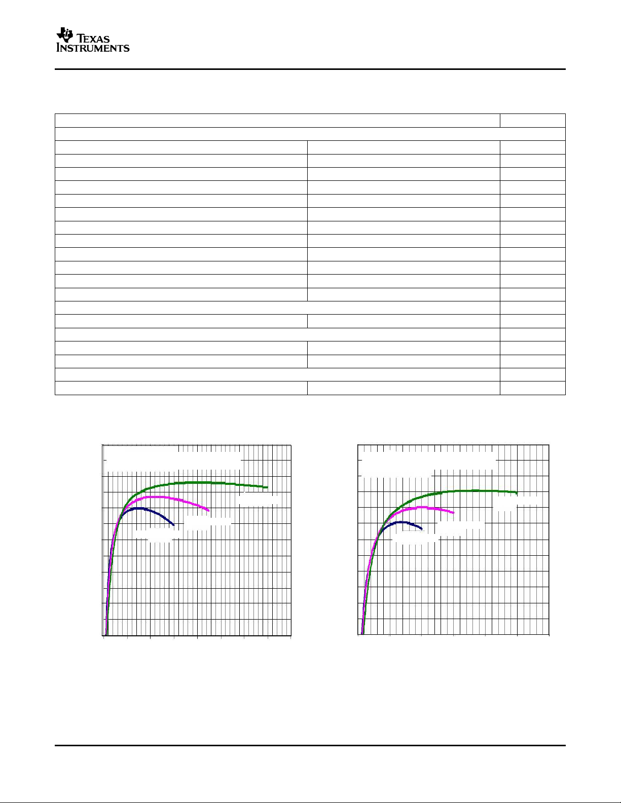
Main Boost Converter
η Efficiency vs Load current Vs=10 V 1
η Efficiency vs Load current Vs=13.5 V 2
η Efficiency vs Load current Vs=15 V 3
f
SW
Negative Charge Pump Driver
V
GL
Positive Charge Pump Driver
V
GH
V
GH
VCOM Buffer
Switching frequency vs Input voltage and temperature 4
PWM operation at nominal load current 5
PWM operation at light load current 6
Load transient response 7
Softstart boost converter 8
Power-on sequencing 9
Power-on sequencing External MOSFET in series to Vs 10
Gate voltage shaping of V
GH
Adjustable Fault detection 12
V
GL
V
GH
V
GH
vs load current 13
vs load current; Charge pump doubler stage 14
vs load current; Charge pump tripler stage 15
VCOM Buffer transconductance 16
11
EFFICIENCY EFFICIENCY
vs vs
LOAD CURRENT LOAD CURRENT
Figure 1. Figure 2.
7
www.ti.com
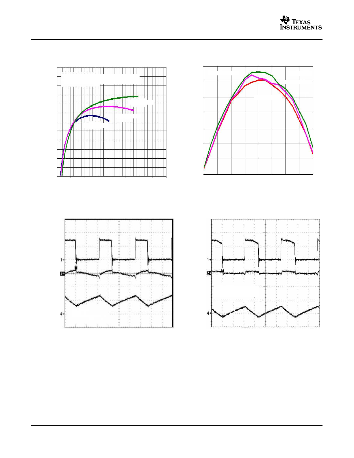
−40 −20 0 20 40 60 80 100 120
1.155
1.150
1.145
1.140
1.135
1.130
1.125
1.120
VS = 13.5 V
VIN = 7 V
VIN = 3.6 V
V
IN
= 1.8 V
f − Frequency − MHz
TA − Free-Air Temperature − C
0 0.05 0.1 0.15 0.2
100
90
80
70
60
50
40
Efficiency − %
IO − Load Current − A
0.25 0.3 0.35 0.4
VS = 15 V ,
VGH = VGL = No Load, Switching
VIN = 2.5 V
VIN = 3.3 V
VIN = 5 V
VIN = 5 V ,
VO = 13.5 V/300 mA
250 ns/div
V
SW
10 V/div
V
O
50 mV/div
I
L
1 A/div
V
SW
10 V/div
V
O
50 mV/div
I
L
1 A/div
VIN = 5 V
VO = 13.5 V/10 mA
250 ns/div
TPS65150
SLVS576 – SEPTEMBER 2005
EFFICIENCY SWITCHING FREQUENCY
vs vs
LOAD CURRENT TEMPERATURE
PWM OPERATION PWM OPERATION
NOMINAL LOAD CURRENT LIGHT LOAD CURRENT
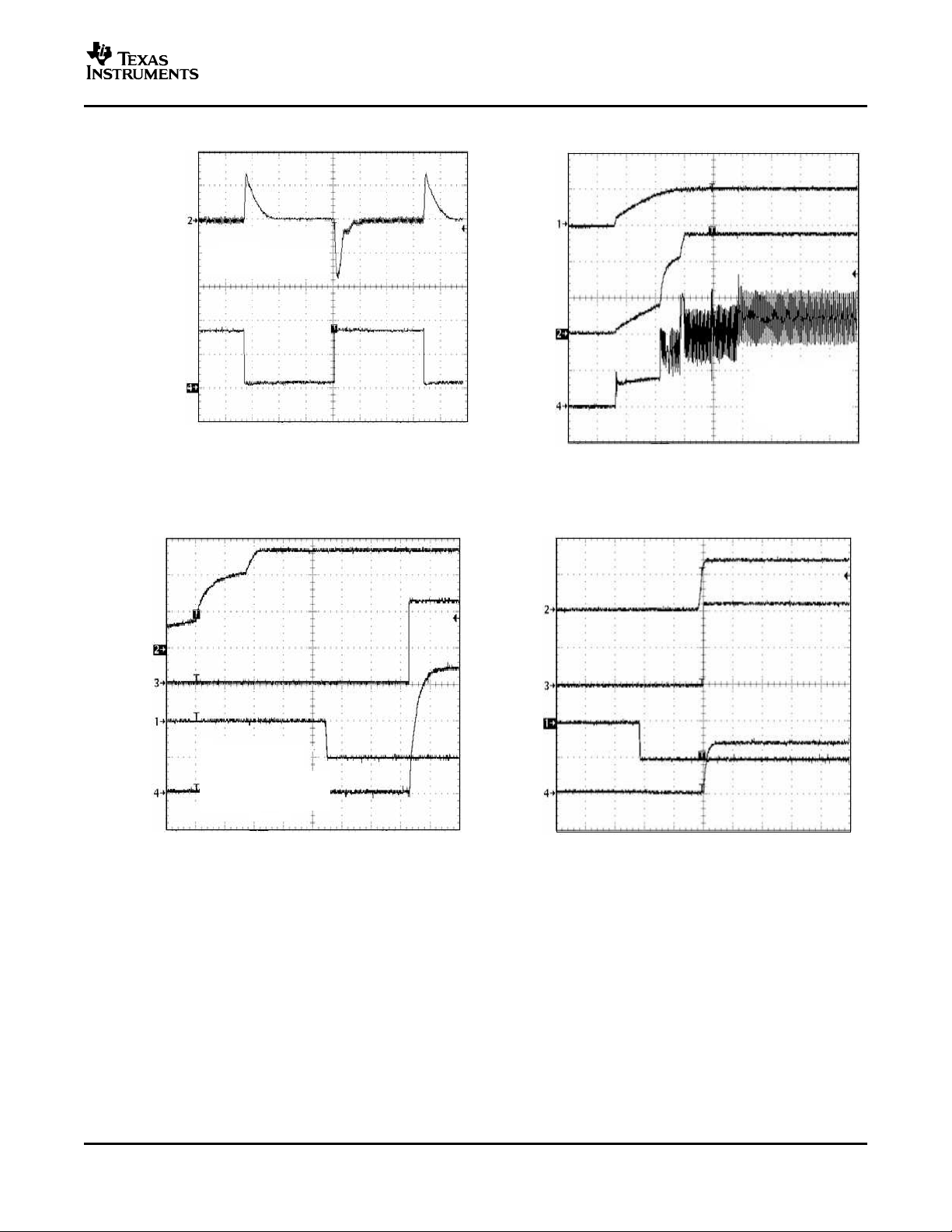
Figure 3. Figure 4.
Figure 5. Figure 6.
8
www.ti.com
VO1
100 mV/div
I
O
30 mA to 330 mA
VIN = 3.3 V
VS = 10 V, CO = 22 F
100 s/div
V
IN
5 V/div
V
S
5 V/div
I
IN
500 mA/div
VIN = 5 V
VO = 13.5 V
I
out
= 200 mA
2.5 ms/div
V
S
5 V/div
VGH
10 V/div
VGL
5 V/div
VCOM
2 V/div
1 ms/div
VIN = 5 V
VO = 13.6 V/ 300 mA
VCOM CIN = 1 nF
V
S
5 V/div
VGH
10 V/div
VGL
5 V/div
VCOM
5 V/div
2.5 ms/div
LOAD TRANSIENT RESPONSE SOFT START BOOST CONVERTER
Figure 7. Figure 8.
TPS65150
SLVS576 – SEPTEMBER 2005
POWER-ON SEQUENCING POWER-ON SEQUENCING WITH
EXTERNAL ISOLATION MOSFET AT V
Figure 9. Figure 10.
S
9
www.ti.com
V
S
5 V/div
VGH
10 V/div
VGL
5 V/div
Fault Delay Time
Fault
(Heavy Load at V
S
)
CFDLY = 100 nF
10 ms/div
CTRL
2 V/div
VGH
10 V/div
2.5 s/div
C
ADJ
= 68 pF
VGH = No Load
−4.86
−4.88
−4.90
−4.92
−4.94
−4.96
−4.98
−5.00
−5.02
0 0.02 0.04 0.06 0.08 0.1
VS = 10 V
VGL = –5 V
VGL − Gate Voltage Low − V
IO − Load Current − A
TA = 85C
TA = 25C
TA = −40C
25
24.50
24
23.50
23
22.50
22
21.50
21
20.50
20
0 0.02 0.04 0.06 0.08 0.1
VS = 15 V
VGH = 24 V
x2 Stage
TA = 85C
TA = 25C
TA = −40C
IO − Load Current − A
VGH − Gate Voltage High − V
TPS65150
SLVS576 – SEPTEMBER 2005
GATE VOLTAGE SHAPING V
GH
ADJUSTABLE FAULT DETECTION
Figure 11. Figure 12.
VGL– GATE VOLTAGE LOW V
vs vs
LOAD CURRENT LOAD CURRENT –X2 STAGE
– GATE VOLTAGE HIGH
GH
10
Figure 13. Figure 14.

www.ti.com
0 0.02 0.04 0.06 0.08 0.1
25
24.50
23.50
24
23
22.50
22
21.50
21
22.50
20
VS = 10 V
VGH = 24 V
x3 Stage
TA = 25C
TA = −40C
IO − Load Current − A
VGH − Gate Voltage High − V
TA = 85C
0.08
0.06
0.04
0.02
0
−0.02
−0.04
−0.06
−0.08
−150 −100 −50 0 50 100 150
VS = 10 V
V
VCOM
= 5 V
VCOM Buffer − V
IO − Load Current − A
TPS65150
SLVS576 – SEPTEMBER 2005
VGH– GATE VOLTAGE HIGH VCOM BUFFER dV
vs vs
LOAD CURRENT – X3 STAGE LOAD CURRENT
Figure 15. Figure 16.
OUT
11
www.ti.com
Current
Control
Soft Start
1.2 MHz
Oscillator
VFB
1.154V
Comparator
GM Amplifier
Sawtooth
Generator
VFB
1.154
SUP
SUP
DRVP
FBP
Vref
1.213V
Vref
1.213V
Bias Vref=1.213V
Logic Control Block
Shutdown Latch Timer
Thermal Shutdown
DLY1
CTRL
ADJ
REF
FBN
DRVN
COMP
FB
VIN
SW SW
FDLY
VCOM
GND
Q1
Q3
Q4
SUP
Reference
Output
Negative
Charge Pump
Positive
Charge Pump
Main boost
converter
Vref
1.213V
Current
Control
Softstart
SUP
(Vout)
GM Amplifier
Low Gain
Current Limit
and
Soft Start
Control
Logic
Gate Drive circuit
Q2
SUP
I
DLY1
Vin
Vref
DL1
Delay Between
Vs and VGL
Gate Voltage
Control Circuit
IN
Q5
I
ADJ
Q6
Vref
1.213V
UVLO
CPI
Q7
Control
CTRL,EN,FBP=high
Q11=Q13=on, Q12=off
CTRL=low
Q11=Q13off, Q12=on
I
DRVP
I
DRVN
I
DLY2
Vin
Vref
Delay Between
VGL and VGH
DLY2
PGND
PGND
DL2
DL1 DL2
SUP
Soft Start
Q11
Q12
VCOM
Buffer
Disable
Main Boost
Soft Start
Completed
Main Boost
Power Good
GD
VGH
ADJ
Gate Drive
SUP
ADJ
TPS65150
SLVS576 – SEPTEMBER 2005
FUNCTIONAL BLOCK DIAGRAM
12

www.ti.com
TPS65150
SLVS576 – SEPTEMBER 2005
DETAILED DESCRIPTION
Main Boost Converter
The main boost converter operates with pulse width modulation (PWM) and a fixed switching frequency of 1.2
MHz. The converter uses an unique fast response, voltage mode controller scheme with input voltage
feedforward. This achieves excellent line and load regulation (0.16%/A load regulation typical) and allows the use
of small external components. To add higher flexibility to the selection of external component values the device
uses external loop compensation. Although the boost converter looks like a non-synchronous boost converter
topology operating in discontinuous conduction mode at light load current the TPS65150 maintains continuous
conduction even at light load currents. This is achieved by using the Virtual Synchronous Converter Technology
having an external Schottky diode with an integrated MOSFET in parallel connected between SW pin and the
SUP pin. See Functional Block Diagram. The intention of this MOSFET is to allow the current to go below ground
which is the case at light load conditions. For this purpose a small integrated P-Channel MOSFET, with typically
10- Ω R
voltage conducts the current. This causes the converter to operate with a fixed frequency in continuous
conduction mode over the entire load current range. This avoids the ringing on the switch pin as seen with
standard non-synchronous boost converter and allows a simpler compensation for the boost converter.
Soft Start
The main boost converter as well as the charge pump driver have an internal soft-start circuit. This avoids heavy
voltage drops at the input voltage rail or at the output of the main boost converter Vs during startup caused by
high inrush currents. As the main boost converter starts up the internal current limit threshold is increased in
three steps. The device starts with the first step where the current limit is set to 2/5 of the typical current limit (2/5
of 2.3 A) for 2048 clock cycles then increased to 3/5 of the current limit for 2048 clock cycles and the 3
the full current limit. This gives a typical start-up time around 5 ms.
, is sufficient. When the inductor current is positive the external Schottky diode with the lower forward
DS(on)
rd
step is
Adjustable Fault Delay
The TPS65150 has an adjustable delay timer integrated shutting down the entire device in case of a fault at the
outputs. The fault timer is also active during startup. Connecting a capacitor from the FDLY pin to Vin sets the
delay time, from the point where one of the outputs (VS, VGH, VGL) drops below its power good threshold, until
the device enters the shutdown latch. Since the fault delay timer is also active during startup, the device enters
shutdown when the output voltage of the main boost converter, Vs, does not reach its power-good threshold after
the fault delay time has passed. When an external isolation switch is used, shown in Figure 24, then the device
provides short circuit protection even during start-up. To restart the device, the input voltage has to be cycled to
GND. The shutdown function can be disabled by connecting FDLY to VIN. The fault delay time is calculated as:
tF= C × R = C × 450 k Ω = 100 nF × 450 k Ω ≈ 40 ms
Positive Charge Pump
The positive charge pump provides a regulated output voltage, set by the external resistor divider. Figure 17
shows an extract of the positive charge pump driver circuit out of the block diagram. The operation of the charge
pump driver can be understood best by looking at Figure 17 . During the first cycle Q3 is turned on and the flying
capacitor, Cfly, is charged to the source voltage, Vs. During the next clock cycle Q3 is turned off, and the current
source charges the drive pin, DRVP, up to the supply voltage, VSUP. Since the flying capacitor voltage sits on
top of the drive pin voltage the maximum output voltage is VGH=Vsup + Vs - Vdrop. Vdrop is the voltage drop
across the external diodes and internal charge pump MOSFETs.
13

www.ti.com
Q3
I
DRVP
DRVP
Current
Control
Soft Start
FBP
Cfly
Vs
R5
R6
C13
0.47 F
VGH
23 V/50 mA
SUP = VIN for V
S
> = 15 V
SUP = VS for V
S
< = 15 V
V
out
1.2131
R5
R6
R5 R6
V
out
V
FB
1 R6
V
out
1.213
1
V
out
V
REF
R3
R4
1.213 V
R3
R4
R3 R4
V
out
V
REF
R4
V
out
1.213
TPS65150
SLVS576 – SEPTEMBER 2005
DETAILED DESCRIPTION (continued)
Figure 17. Extract of the Positive Charge Pump Driver
If higher output voltages are required another charge pump stage can be added to the output, as shown in Figure
21 at the end of the data sheet. To minimize quiescent current a high impedance feedback divider should be
used. The top feedback resistor should not be selected larger than 1M Ω .
Setting the output voltage:
Negative Charge Pump
The negative charge pump provides a regulated output voltage set by the external resistor divider. The negative
charge pump operates very similar to the positive charge pump with the difference that the voltage on the supply
pin SUP is inverted. The maximum output voltage for a single stage charge pump inverter is VGL = (–VSUP) +
Vdrop. Vdrop is the voltage drop across the external diodes and internal charge pump MOSFETs.
Setting the output voltage:
The lower feedback resistor value, R4, should range between 40 k Ω to 120 k Ω ; or, the overall feedback
resistance should be within 500 k Ω to 1 M Ω . Smaller values load the reference too heavily; and larger values
may cause stability problems. The negative charge pump requires two external Schottky diodes. The peak
current rating of the Schottky diode has to be twice the load current of the output. For a 20-mA output current,
the BAT54 dual Schottky diode is a good choice.
(1)
(2)
14

www.ti.com
VGL
DLY1
VGH, with CTRL=high
DLY2
VIN
GD
Vs
Fall Time of VS, VGL and
VGH Depends on Load
Current and Feedback
Resistor Impedance
C
dly
5 A td
V
REF
5 A td
1.213 V
with td Desired delay time
TPS65150
SLVS576 – SEPTEMBER 2005
DETAILED DESCRIPTION (continued)
Power-on Sequencing, DLY1, DLY2
As soon as the input voltage is applied, and rises above the undervoltage lockout (UVLO), the device starts with
the main boost converter, Vs, coming up first. Then the negative voltage, VGL, comes up, set by the delay time
DLY1; and then the positive charge pump, VGH, set by the delay time DLY2. Finally, the VCOM buffer starts up.
The delay times, DLY1 and DLY2, are set by the capacitor value connected to these pins. An internal current
source charges the capacitor with a constant current of typically 5 µA until the voltage reaches the internal
comparator trip point of Vref = 1.213 V.
Figure 18. Power on Sequencing With CTRL = High
Setting the Delay Times DLY1, DLY2
Connecting an external capacitor to the DLY1 and DLY2 pins sets the delay time. If no delay time is required,
these pins can be left open. To set the delay time, the external capacitor connected to DLY1 and DLY2 is
charged with a constant current source of typically 5 µA . The delay time is terminated when the capacitor
voltage has reached the internal reference voltage of Vref = 1.213 V. The external delay capacitor is calculated:
Gate Drive, GD
The gate drive pin can be used to drive an external MOSFET, providing isolation for the main boost converter Vs.
The gate drive is an open drain output capable of sinking typically 500 µA. The gate drive is latched low as soon
as the main boost converter, Vs, reaches its power-good threshold. The gate drive signal goes high impedance
when the input voltage falls below the undervoltage lockout (UVLO) or the device enters shutdown latch triggered
by the fault delay.
VGH Switch / Gate Voltage Shaping, CPI – VGH
The gate voltage shaping circuit is used to reduce crosstalk between the LCD pixels by adjusting the fall time of
the positive gate voltage, VGH. The CTRL pin needs to be connected to Vin if the gate voltage shaping function
is not used. This function is implemented by adjusting the fall time of the gate voltage signal, VGH, generated by
the positive charge pump. The fall time can be adjusted with the external capacitor, Cadj connected to the ADJ
pin. The corresponding timing diagram is shown in Figure 20 .
(3)
15

www.ti.com
VGH
Q5
I
ADJ
Q6
Vref
1.213 V
CTRL
UVLO
ADJ
CPI
FBP
Cadj
47 pF
Q7
Control
CTRL, UVOL, FPB = High
Q5 = Q7 = ON, Q6 = OFF
CTRL = Low
Q5 = Q7 = OFF, Q6 = T urns ON
toff
VGH
VCPI
VL
ton
toffIadj x
Cadj
V
Control
Signal
(Pin CTRL)
V
Cadj
Iadj toff
V
with ladj 200 A
TPS65150
SLVS576 – SEPTEMBER 2005
DETAILED DESCRIPTION (continued)
Figure 19. Implementation of the Gate voltage shaping
Figure 20. Timing Diagram of the Gate voltage shaping
The control signal applied to CTRL sets the timing of VGH. When CTRL is high, Q5 is turned on and the positive
charge pump voltage applied on CPI is present on VGH. At the same time, the capacitor connected to ADJ is
charged up by Q7 to VGH, while Q6 is turned off. When CTRL is taken low, Q5 and Q7 turn off, and Q6 is slowly
turned on as the capacitor on ADJ is discharged by the discharge current I
value on C
desired voltage drop, ∆ V.
When the input voltage falls below the undervoltage threshold (UVLO) or the device enters shutdown latch
determines the fall time of VGH. For a given off time (toff), external capacitor Cadj determines the
ADJ
, typically 200 µA. The capacitor
ADJ
triggered by the fault delay timer, then VGH is disconnected from CPI by Q5 and is high impedance.
16
(4)

www.ti.com
1. Duty Cycle : D 1
Vin
Vout
2. Maximum output current : I
out
Isw
Vin D
2 ƒs L
(1 D)
3. Peak switch current : I
swpeak
Vin D
2 ƒs L
I
out
1 D
TPS65150
SLVS576 – SEPTEMBER 2005
DETAILED DESCRIPTION (continued)
Thermal Shutdown
A thermal shutdown is implemented to prevent damage because of excessive heat and power dissipation.
Typically, the thermal shutdown threshold is 155 ° C . When this threshold is reached, the device enters shutdown.
The device can be enabled again by cycling the input voltage to GND.
Vcom Buffer
The VCOM Buffer is a transconductance amplifier designed to drive capacitive loads. The IN pin is the input of
the VCOM buffer. If the VCOM buffer is not required for certain applications, it is possible to shut down the
VCOM buffer by connecting IN to ground, reducing the overall quiescent current. The VCOM buffer features a
soft start, avoiding a large voltage drop at Vs during startup. The VCOM buffer input, IN, cannot be pulled
dynamically to ground during operation.
Boost Converter Design Procedure
The first step in the design procedure is to verify whether the maximum possible output current of the boost
converter supports the specific application requirements. A simple approach is to estimate the converter
efficiency, by taking the efficiency numbers from the provided efficiency curves, or use a worst case assumption
for the expected efficiency, e.g. 75%.
(5)
With
Isw = Converter switch current (minimum switch current limit = 2.0 A)
fs = Converter switching frequency (typical 1.2 MHz)
L = Selected inductor value
η = Estimated converter efficiency (use the number from the efficiency plots, or 0.75 as an estimation)
The peak switch current is the steady-state peak switch current that the integrated switch, inductor, and external
Schottky diode has to be able to handle. The calculation must be done for the minimum input voltage where the
peak switch current is highest. For the calculation of the maximum current delivered by the boost converter it
needs to be considered that the positive and negative charge pumps as well as the VCOM buffer run from the
output of the boost converter as well.
Inductor Selection
Several inductors work with the TPS65150. Especially with external compensation, the performance can be
adjusted to the specific application requirements. The main parameter for the inductor selection is the inductor
saturation current, which should be higher than the peak switch current as calculated previously with additional
margin to cover for heavy load transients. The alternative, more conservative approach, is to choose the inductor
with a saturation current at least as high as the typical switch current limit of 2.5 A. The second important
parameter is the inductor DC resistance. Usually the lower the DC resistance the higher the efficiency. It is
important to note that the inductor DC resistance is not the only parameter determining the efficiency. For a
boost converter, where the inductor is the energy storage element, the type and material of the inductor
influences the efficiency as well. Especially at high switching frequencies of 1.2 MHz, inductor core losses,
proximity effects, and skin effects become more important. Usually an inductor with a larger form factor gives
higher efficiency. The efficiency difference between different inductors can vary between 2% to 10%. For the
TPS65150, inductor values between 3.3 µH and 6.8 µH are a good choice, but other values can be used as well.
Possible inductors are shown in Table 1 .
(6)
(7)
17

www.ti.com
D 1
Vin
Vout
I
avg
(1 D) Isw
Vin
Vout
2.0 A with lsw minimum switch current
of the TPS65150 (2.0 A)
TPS65150
SLVS576 – SEPTEMBER 2005
DETAILED DESCRIPTION (continued)
Table 1. Inductor Selection
INDUCTOR VALUE COMPONENT SUPPLIER DIMENSIONS IN mm Isat – DC Resistance
4.7 µH Coilcraft DO1813P-472HC 8,89 × 6,1 × 5,0 2.6 A – 54 m Ω
4.2 µH Sumida CDRH5D28 4R2 5,7 × 5,7 × 3 2.2 A – 23 m Ω
4.7 µH Sumida CDC5D23 4R7 6 × 6 × 2,5 1.6 A – 48 m Ω
4.2 µH Sumida CDRH6D12 4R2 6,5 × 6,5 × 1,5 1.8 A – 60 m Ω
3.9 µH Sumida CDRH6D28 3R9 7,0 × 7,0 × 3,0 2.6A – 20 m Ω
3.3 µH Sumida CDRH6D12 4R2 6,5 × 6,5 × 1,5 1.9 A – 50 m Ω
Output Capacitor Selection
For best output voltage filtering, a low ESR output capacitor is recommended. Ceramic capacitors have a low
ESR value, but tantalum capacitors can be used as well, depending on the application. A 22-µF ceramic output
capacitor works for most applications. Higher capacitor values can be used to improve the load transient
regulation. See Table 2 for the selection of the output capacitor.
Input Capacitor Selection
For good input voltage filtering, low ESR ceramic capacitors are recommended. A 22-µF ceramic input capacitor
is sufficient for most applications. For better input voltage filtering, this value can be increased. See Table 2 , and
Typical Applications for input capacitor recommendations.
Table 2. Input and Output Capacitor Selection
CAPACITOR VOLTAGE RATING COMPONENT SUPPLIER COMMENTS
22 µF/1206 16 V Taiyo Yuden EMK325BY226MM Cout
22 µF/1206 6.3 V Taiyo Yuden JMK316BJ226 Cin
Rectifier Diode Selection
To achieve high efficiency, a Schottky diode should be used. The reverse voltage rating should be higher than
the maximum output voltage of the converter. The required average rectified forward current rating of the
Schottky diode is calculated as the off time of the converter times the maximum switch current of the TPS65150:
Usually, a Schottky diode with 1-A maximum average rectified forward current rating is sufficient for most of the
applications. Secondly, the Schottky rectifier has to be able to dissipate the power. The dissipated power is the
average rectified forward current times the diode forward voltage.
PD = Iavg × VF = Isw × (1 – D) × VF with lsw = minimum switch current of the TPS65150 (2.0 A).
Typically, the diode should be able to dissipate 270 mW maximum depending on the load current and forward
voltage. In terms of efficiency, the main parameters of the diode are the forward voltage and the reverse leakage
current of the diode; both should be as low as possible.
Table 3. Rectifier Diode Selection
CURRENT RATING Vr V
Iavg
2 A 20 V 0.44 V at 2 A SL22, Vishay Semiconductor
2 A 20 V 0.5 V at 2 A SS22, Fairchild Semiconductor
1 A 30 V 0.44 V at 2 A MBRS130L, Fairchild Semiconductor
1 A 20 V 0.45 V at 1 A UPS120, Microsemi
1 A 20 V 0.45 V at 1 A MBRM120, ON Semiconductor
forward
COMPONENT SUPPLIER
(8)
(9)
18

www.ti.com
V
out
1.146 V1
R1
R2
C
FF
1
2 ƒz R1
1
2 8.8 kHz R1
TPS65150
SLVS576 – SEPTEMBER 2005
Setting the Output Voltage
The output voltage is set by the external resistor divider and is calculated as:
To minimize quiescent current high impedance feedback resistors should be used. The upper feedback resistor
R1 should not be larger than 1M Ω . Across the upper resistor, a bypass capacitor is required to speed up the
circuit during load transients. The capacitor value is selected according to Table 4 and the formula (12) as shown
in the next section.
Compensation (COMP) and feedforward capacitor
The regulator loop can be compensated by adjusting the external components connected to the COMP pin. The
COMP pin is the output of the internal transconductance error amplifier. The compensation capacitor adjusts the
low-frequency gain. Adding a resistor in series to it will increase the high frequency gain. Since the converter
gain changes with the input voltage different compensation capacitors are required. Lower input voltages require
a higher gain, and therefore a smaller compensation capacitor value.
(10)
Table 4. Compensation Components for different V
V
IN
2.5 V 470 pF 68 k Ω 8.8 kHz
3.3 V 470 pF 33 k Ω 7.8 kHz
5.0 V 2.2 nF 0 k Ω 11.2 kHz
C
COMP
R
COMP
Voltages
IN
f
Z
The feedforward capacitor across the feedback resistor devider of the boost converter sets an additional zero at
the frequency fz to compensate the loop. Typical values for fz are shown in Table 4 giving a feedforward
capacitor value as calculated below.
Please refer to the typical application circuits at the end of the datasheet for detailed circuit configurations and
values.
Layout Consideration
The PCB layout is an important step in the power supply design. An incorrect layout could cause converter
instability, load regulation problems, noise, and EMI issues. Especially with a switching dc-dc converter at
high load currents, too-thin PCB traces can cause significant voltage spikes. Good grounding becomes
important as well. If possible, a common ground plane to minimize ground shifts between analog (GND) and
power ground (PGND) is recommended. Additionally, the following PCB design layout guidelines are
recommended for the TPS65150:
1. Boost converter output capacitor, input capacitor and Power ground (PGND) should form a star ground or
should be directly connected together on a common power ground plane.
2. Place the input capacitor directly from the input pin (VIN) to ground.
3. Use a bold PCB trace to connect SUP to the output Vs.
4. Place a small baypass capacitor from the SUP pin to ground.
5. Use short traces for the charge-pump drive pins (DRVN, DRVP) of VGH and VGL because these traces
carry switching currents.
6. Place the charge pump flying capacitors as close as possible to the DRVP and DRVN pin, avoiding a high
voltage spikes at these pins.
7. Place the Schottky diodes as close as possible to the IC, respectively to the flying capacitors connected to
DRVP and DRVN.
8. Carfully route the chare pump traces to avoid interference with other circuits since they carry high voltage
switching currents .
9. Place the output capacitor of the VCOM buffer as close as possible to the output pin (VCOM).
(11)
19

www.ti.com
TPS65150
SLVS576 – SEPTEMBER 2005
10. The power pad of the TSSOP package needs to be soldered to the PCB for imroved thermal performance.
11. The thermal pad of the QFN package needs to be soldered to the PCB for reliability and thermal
performance reasons.
20

www.ti.com
VIN
DRVN
FBN
REF
COMP
DLY1
DLY2
FDLY
SW SW
SUP
DRVP
GD
CPI
FBP
GND
PGND
PGND
VCOM
TPS65150
D1
D2
D3
ADJ
CTRL
VGH
23 V/20 mA
VGH
VGH
Contol Signal
D4
D5
D6 D7
FB
SW
IN
CPI
CPI
VCOM
Output
R8
500 k
R7
500 k
C6 1 nF
L1
3.9 H
C1
22 F
C7
0.33 F
R3
620 k
R4
150 k
C3
0.33 F
C8
220 nF
R9
33 k
C9
470 pF
C10 C11 C12
22 pF
10 nF
10 nF
C5
1 F
0.33 F
C16
C17
0.33 F
C4
0.33 F
C18
0.33 F
R5
1 M
R6
56 k
C2
22 F
Vs
10 V/400 mA
R2
56 k
R2
430 k
C15
33 pF
C14
1 F
VGL
−5 V/20 mA
Vin
3.3 V
C13
100 nF
V
IN
VIN
DRVN
FBN
REF
COMP
DLY1
DLY2
FDLY
SW SW
SUP
DRVP
GD
CPI
FBP
GND
PGND
PGND
VCOM
TPS65150
D1
D2
D3
ADJ
CTRL
VGH
23 V/20 mA
VGH
VGH
Contol Signal
D4
D5
D6 D7
FB
SW
IN
CPI
CPI
VCOM
Output
R8
500 k
R7
500 k
C6 1 nF
L1
3.9 H
C1
22 F
C7
0.33 F
R3
620 k
R4
150 k
C3
0.33 F
C8
220 nF
R9
68 k
C9
470 pF
C10 C11 C12
22 pF
10 nF
10 nF
C5
1 F
0.33 F
C16
C17
0.33 F
C4
0.33 F
C18
0.33 F
R5
1 M
R6
56 k
C2
22 F
Vs
10 V/280 mA
R2
56 k
R2
430 k
C15
47 pF
C14
1 F
VGL
−5 V/20 mA
Vin
2.5 V
C13
100 nF
V
IN
TPS65150
SLVS576 – SEPTEMBER 2005
APPLICATION INFORMATION
Figure 21. Notebook LCD Supply powered from a 3.3V rail
Figure 22. Notebook LCD Supply powered from a 2.5V rail
21

www.ti.com
VIN
DRVN
FBN
REF
COMP
DLY1
DLY2
FDLY
SW SW
SUP
DRVP
GD
CPI
FBP
GND
PGND
PGND
VCOM
TPS65150
D3
ADJ
CTRL
VGH
VGH
Contol Signal
D5
FB
IN
CPI
CPI
D1
D2
D4
R8
500 k
R7
500 k
C6 1 nF
L1
3.9 H
C1
22 F
0.33 F
C2
22 F
Vs
13.5 V/450 mA
R2
75 k
C15
22 pF
C14
1 F
Vin
5 V
R1
820 k
C7
R3
620 k
R4
150 k
C3
0.33 F
C8
220 nF
C9
2.2 nF
0.33 F
C16
C4
0.33 F
R5
1 M
VGL
−5 V/20 mA
R6
56 k
C5
1 F
VGH
23 V/20 mA
C10 C11 C12
22 pF 10 nF 10 nF
VCOM
Output
C13
100 nF
V
IN
GD
C13
1 Fm
Q1
Vs
13.5 V/450 mA
VIN
DRVN
FBN
REF
COMP
DLY1 DLY2 F D LY
SW SW
SUP
DRVP
GD
CPI
FBP
GND
PGND
PGND
VCOM
TPS65150
D1
Vin
5 V
D2
D3
R5
1M
R6
56k
C2
22 Fm
C 15
22 pF
ADJ
CTRL
VGH
23 V/20 mA
VGH
VGH
Contol Signal
D4
D5
VGL
-5 V/20 mA
FB
C14
1 Fm
IN
C6
1 nF
R8
500 kW
R3
620 kW
R2
75 kW
R1
820 kW
R8
100 kW
R7
510 kW
R4
150 kW
R7
500 kW
L1
3.9 Hm
C1
22 Fm
C7
0.33 Fm
C16
0.33 Fm
C4
0.33 Fm
C3
0.33 Fm
C8
220 nF
C9
2.2 nF
C10
22 pF
C11
11 nF
C12
10 nF
C13
100 nF
CPI
CPI
V COM
Output
C5
1 Fm
VIN
C17
220 nF
SI2343
TPS65150
SLVS576 – SEPTEMBER 2005
APPLICATION INFORMATION (continued)
Figure 23. Monitor LCD Supply powered from a 5V rail
Figure 24. Typical Isolation and Short-Circuit Protection Switch for Vs using Q1 and Gate Drive Signal
22
(GD)
PACKAGE OPTION ADDENDUM
www.ti.com
18-Jul-2006
PACKAGING INFORMATION
Orderable Device Status
(1)
Package
Type
Package
Drawing
Pins Package
Qty
Eco Plan
TPS65150PWP ACTIVE HTSSOP PWP 24 60 Green (RoHS &
no Sb/Br)
TPS65150PWPG4 ACTIVE HTSSOP PWP 24 60 Green (RoHS &
no Sb/Br)
TPS65150PWPR ACTIVE HTSSOP PWP 24 2000 Green (RoHS &
no Sb/Br)
TPS65150PWPRG4 ACTIVE HTSSOP PWP 24 2000 Green (RoHS &
no Sb/Br)
TPS65150RGER ACTIVE QFN RGE 24 3000 Green (RoHS &
no Sb/Br)
TPS65150RGERG4 ACTIVE QFN RGE 24 3000 Green (RoHS &
no Sb/Br)
(1)
The marketing status values are defined as follows:
ACTIVE: Product device recommended for new designs.
LIFEBUY: TI has announced that the device will be discontinued, and a lifetime-buy period is in effect.
NRND: Not recommended for new designs. Device is in production to support existing customers, but TI does not recommend using this part in
a new design.
PREVIEW: Device has been announced but is not in production. Samples may or may not be available.
OBSOLETE: TI has discontinued the production of the device.
(2)
Lead/Ball Finish MSL Peak Temp
CU NIPDAU Level-2-260C-1 YEAR
CU NIPDAU Level-2-260C-1 YEAR
CU NIPDAU Level-2-260C-1 YEAR
CU NIPDAU Level-2-260C-1 YEAR
CU NIPDAU Level-2-260C-1 YEAR
CU NIPDAU Level-2-260C-1 YEAR
(3)
(2)
Eco Plan - The planned eco-friendly classification: Pb-Free (RoHS), Pb-Free (RoHS Exempt), or Green (RoHS & no Sb/Br) - please check
http://www.ti.com/productcontent for the latest availability information and additional product content details.
TBD: The Pb-Free/Green conversion plan has not been defined.
Pb-Free (RoHS): TI's terms "Lead-Free" or "Pb-Free" mean semiconductor products that are compatible with the current RoHS requirements
for all 6 substances, including the requirement that lead not exceed 0.1% by weight in homogeneous materials. Where designed to be soldered
at high temperatures, TI Pb-Free products are suitable for use in specified lead-free processes.
Pb-Free (RoHS Exempt): This component has a RoHS exemption for either 1) lead-based flip-chip solder bumps used between the die and
package, or 2) lead-based die adhesive used between the die and leadframe. The component is otherwise considered Pb-Free (RoHS
compatible) as defined above.
Green (RoHS & no Sb/Br): TI defines "Green" to mean Pb-Free (RoHS compatible), and free of Bromine (Br) and Antimony (Sb) based flame
retardants (Br or Sb do not exceed 0.1% by weight in homogeneous material)
(3)
MSL, Peak Temp. -- The Moisture Sensitivity Level rating according to the JEDEC industry standard classifications, and peak solder
temperature.
Important Information and Disclaimer:The information provided on this page represents TI's knowledge and belief as of the date that it is
provided. TI bases its knowledge and belief on information provided by third parties, and makes no representation or warranty as to the
accuracy of such information. Efforts are underway to better integrate information from third parties. TI has taken and continues to take
reasonable steps to provide representative and accurate information but may not have conducted destructive testing or chemical analysis on
incoming materials and chemicals. TI and TI suppliers consider certain information to be proprietary, and thus CAS numbers and other limited
information may not be available for release.
In no event shall TI's liability arising out of such information exceed the total purchase price of the TI part(s) at issue in this document sold by TI
to Customer on an annual basis.
Addendum-Page 1


IMPORTANT NOTICE
Texas Instruments Incorporated and its subsidiaries (TI) reserve the right to make corrections, modifications,
enhancements, improvements, and other changes to its products and services at any time and to discontinue
any product or service without notice. Customers should obtain the latest relevant information before placing
orders and should verify that such information is current and complete. All products are sold subject to TI’s terms
and conditions of sale supplied at the time of order acknowledgment.
TI warrants performance of its hardware products to the specifications applicable at the time of sale in
accordance with TI’s standard warranty. Testing and other quality control techniques are used to the extent TI
deems necessary to support this warranty . Except where mandated by government requirements, testing of all
parameters of each product is not necessarily performed.
TI assumes no liability for applications assistance or customer product design. Customers are responsible for
their products and applications using TI components. To minimize the risks associated with customer products
and applications, customers should provide adequate design and operating safeguards.
TI does not warrant or represent that any license, either express or implied, is granted under any TI patent right,
copyright, mask work right, or other TI intellectual property right relating to any combination, machine, or process
in which TI products or services are used. Information published by TI regarding third-party products or services
does not constitute a license from TI to use such products or services or a warranty or endorsement thereof.
Use of such information may require a license from a third party under the patents or other intellectual property
of the third party, or a license from TI under the patents or other intellectual property of TI.
Reproduction of information in TI data books or data sheets is permissible only if reproduction is without
alteration and is accompanied by all associated warranties, conditions, limitations, and notices. Reproduction
of this information with alteration is an unfair and deceptive business practice. TI is not responsible or liable for
such altered documentation.
Resale of TI products or services with statements different from or beyond the parameters stated by TI for that
product or service voids all express and any implied warranties for the associated TI product or service and
is an unfair and deceptive business practice. TI is not responsible or liable for any such statements.
Following are URLs where you can obtain information on other Texas Instruments products and application
solutions:
Products Applications
Amplifiers amplifier.ti.com Audio www.ti.com/audio
Data Converters dataconverter.ti.com Automotive www.ti.com/automotive
DSP dsp.ti.com Broadband www.ti.com/broadband
Interface interface.ti.com Digital Control www.ti.com/digitalcontrol
Logic logic.ti.com Military www.ti.com/military
Power Mgmt power.ti.com Optical Networking www.ti.com/opticalnetwork
Microcontrollers microcontroller.ti.com Security www.ti.com/security
Low Power Wireless www.ti.com/lpw Telephony www.ti.com/telephony
Video & Imaging www.ti.com/video
Wireless www.ti.com/wireless
Mailing Address: Texas Instruments
Post Office Box 655303 Dallas, Texas 75265
Copyright 2006, Texas Instruments Incorporated
 Loading...