

www.ti.com
Vin
V 1
Uop to 15 V / 400 mA
V 3
Uop to 30 V / 20 mA
V 2
Uop to 12 V / 20 mA
V 4
3.3oV
Vcom
Boost
Converter
Positive Charge
Pump
Negative
Charge Pump
Vcom Buffer
Linear Regulator
Controller
TPS6514x
2.7 V to 5.8 V
SLVS497C – SEPTEMBER 2003 – REVISED APRIL 2006
TRIPLE OUTPUT LCD SUPPLY WITH LINEAR REGULATOR AND POWER GOOD
FEATURES DESCRIPTION
• 2.7-V to 5.8-V Input Voltage Range
• 1.6-MHz Fixed Switching Frequency
• 3 Independent Adjustable Outputs
• Main Output up to 15 V With <1% Typical
Output Voltage Accuracy
• Virtual Synchronous Converter Technology
• Negative Regulated Charge Pump Driver VO2
• Positive Charge Pump Converter VO3
• Auxiliary 3.3-V Linear Regulator Controller
• Internal Soft Start
• Internal Power-On Sequencing
• Fault Detection of all Outputs (TPS65140/45)
• No Fault Detection (TPS65141)
• Thermal Shutdown
• System Power Good
• Available in TSSOP-24 and QFN-24
PowerPAD™ Packages
APPLICATIONS
• TFT LCD Displays for Notebooks
• TFT LCD Displays for Monitors
• Portable DVD Players
• Tablet PCs
• Car Navigation Systems
• Industrial Displays
The TPS6514x series offers a compact and small
power supply solution to provide all three voltages
required by thin film transistor (TFT) LCD displays.
The auxiliary linear regulator controller can be used
to generate a 3.3-V logic power rail for systems
powered by a 5-V supply rail only.
The main output VO1 is a 1.6-MHz fixed frequency
PWM boost converter providing the source drive
voltage for the LCD display. The device is available
in two versions with different internal switch current
limits to allow the use of a smaller external inductor
when lower output power is required. The
TPS65140/41 has a typical switch current limit of 2.3
A and the TPS65145 has a typical switch current
limit of 1.37 A. A fully integrated adjustable charge
pump doubler/tripler provides the positive LCD gate
drive voltage. An externally adjustable negative
charge pump provides the negative gate drive
voltage. Due to the high 1.6-MHz switching
frequency of the charge pumps, inexpensive and
small 220-nF capacitors can be used.
Additionally, the TPS6514x series has a system
power good output to indicate when all supply rails
are acceptable. For LCD panels powered by 5 V the
device has a linear regulator controller using an
external transistor to provide a regulated 3.3 V
output for the digital circuits. For maximum safety,
the TPS65140/45 goes into shutdown as soon as
one of the outputs is out of regulation. The device
can be enabled again by toggling the input or the
enable (EN) pin to GND. The TPS65141 does not
enter shutdown when one of its outputs is below its
power good threshold.
TPS65140 , TPS65141
TPS65145
Please be aware that an important notice concerning availability, standard warranty, and use in critical applications of Texas
Instruments semiconductor products and disclaimers thereto appears at the end of this data sheet.
PowerPAD is a trademark of Texas Instruments.
PRODUCTION DATA information is current as of publication date.
Products conform to specifications per the terms of the Texas
Instruments standard warranty. Production processing does not
necessarily include testing of all parameters.
Copyright © 2003–2006, Texas Instruments Incorporated
www.ti.com
VIN
COMP
GND
EN
ENR
C1+
C1−
DRV
FB2
REF
FB4
BASE
SW
SW
FB1
SUP
C2+
C2−/MODE
OUT3
FB3
PG
PGND
PGND
GND
TPS65140
D1
System Power
Good
Q1
BCP68
D2
D3
R3
R4
R5
R6
C5
R2
R1
V
I
2.7 V to 5.8 V
C3
22 µF
C13
10 nF
L1
4.2 µH
C1 0.22 µF
C12
0.22 µF
C6
0.22 µF
C11
100 nF
V
I
C9
1 µF
VO4
3.3 V
C9
4.7 µF
C1
0.22 µF
V
I
C4
22 µF
C7
0.22 µF
R7
33 kΩ
VO3
Up to 30 V/20 mA
VO1
Up to 15 V/350 mA
VO2
Up to 12 V/20 mA
TPS65140 , TPS65141
TPS65145
SLVS497C – SEPTEMBER 2003 – REVISED APRIL 2006
These devices have limited built-in ESD protection. The leads should be shorted together or the device placed in conductive foam
during storage or handling to prevent electrostatic damage to the MOS gates.
TYPICAL APPLICATION CIRCUIT
ORDERING INFORMATION
(1) (2)
PACKAGE
MARKING
Submit Documentation Feedback
T
A
-40 °C to
85 °C
(1) The PWP and RGE packages are available taped and reeled. Add an R suffix to the device type (TPS65100PWPR) to order the device
taped and reeled. The PWPR package has quantities of 2000 devices per reel, and the the RGER package has 3000 devices per reel.
Without the suffix, the PWP package only, is shipped in tubes with 60 devices per tube.
(2) For the most current package and ordering information, see the Package Option Addendum at the end of this document, or see the TI
Web site at www.ti.com .
LINEAR REGULATOR MINIMUM SWITCH
OUTPUT VOLTAGE CURRENT LIMIT
3.3 V 1.6 A TPS65140PWP TPS65140RGE TPS65140
3.3 V 1.6 A TPS65141PWP TPS65141RGE TPS65141
3.3 V 0.96 A TPS65145PWP TPS65145RGE TPS65145
2
PACKAGE
TSSOP QFN
www.ti.com
TPS65140 , TPS65141
SLVS497C – SEPTEMBER 2003 – REVISED APRIL 2006
ABSOLUTE MAXIMUM RATINGS
over operating free-air temperature range (unless otherwise noted)
Voltages on pin VIN
Voltages on pin VO1, SUP, PG
Voltages on pin EN, MODE, ENR
Voltage on pin SW
Power good maximum sink current (PG) 1 mA
Continuous power dissipation See Dissipation Rating Table
Operating junction temperature range -40 ° C to 150 ° C
Storage temperature range -65 ° C to 150 ° C
Lead temperature (soldering, 10 sec) 260 ° C
(1) Stresses beyond those listed under “absolute maximum ratings” may cause permanent damage to the device. These are stress ratings
only, and functional operation of the device at these or any other conditions beyond those indicated under “recommended operating
conditions” is not implied. Exposure to absolute-maximum-rated conditions for extended periods may affect device reliability.
(2) All voltage values are with respect to network ground terminal.
(2)
(2)
(2)
(2)
DISSIPATION RATINGS
PACKAGE R Θ
24-Pin TSSOP 30.13 C °/W (PWP soldered) 3.3 W 1.83 W 1.32 W
24-Pin QFN 30 C ° /W 3.3 W 1.8 W 1.3 W
JA
(1)
UNIT
-0.3 V to 6 V
-0.3 V to 15.5 V
-0.3 V to VI+ 0.3 V
20 V
TA≤ 25 ° C TA= 70 °C TA= 85 °C
POWER RATING POWER RATING POWER RATING
TPS65145
RECOMMENDED OPERATING CONDITIONS
MIN TYP MAX UNIT
VIN Input voltage range 2.7 5.8 V
L Inductor
T
A
T
J
(1)
4.7 µH
Operating ambient temperature -40 85 °C
Operating junction temperature -40 125 °C
(1) See the application information section for further information.
ELECTRICAL CHARACTERISTICS
Vin= 3.3 V, EN = VIN, VO1 = 10 V, TA= -40 °C to 85 °C, typical values are at TA= 25 ° C (unless otherwise noted)
PARAMETER TEST CONDITIONS MIN TYP MAX UNIT
SUPPLY CURRENT
V
i
I
Q
I
QCharge
I
QEN
I
SD
V
UVLO
LOGIC SIGNALS EN, ENR
V
IH
V
IL
I
I
Input voltage range 2.7 5.5 V
Quiescent current into VIN
Charge pump quiescent
current into SUP
LDO controller quiescent
current into Vin
ENR = GND, VO3 = 2 x VO1, 0.7 0.9 mA
Boost converter not switching
VO1 = SUP = 10 V, VO3 = 2 x VO1 1.7 2.7
VO1 = SUP = 10 V, VO3 = 3 x VO1 3.9 6
ENR = VIN, EN = GND 300 800 µA
Shutdown current into VIN EN = ENR = GND 1 10 µA
Undervoltage lockout VIfalling 2.2 2.4 V
threshold
Thermal shutdown Temperature rising 160 ° C
High level input voltage 1.5 V
Low level input voltage 0.4 V
Input leakage current EN = GND or VIN 0.01 0.1 µA
mA
Submit Documentation Feedback
3
www.ti.com
TPS65140 , TPS65141
TPS65145
SLVS497C – SEPTEMBER 2003 – REVISED APRIL 2006
ELECTRICAL CHARACTERISTICS (continued)
Vin= 3.3 V, EN = VIN, VO1 = 10 V, TA= -40 °C to 85 °C, typical values are at TA= 25 ° C (unless otherwise noted)
PARAMETER TEST CONDITIONS MIN TYP MAX UNIT
MAIN BOOST CONVERTER
VO1 Output voltage range 5 15 V
VO1-Vin 1 V
V
REF
V
FB
I
FB
r
DS(on)
I
LIM
r
DS(on)
I
MAX
I
leak
f
SW
NEGATIVE CHARGE PUMP VO2
VO2 Output voltage range -2 V
V
ref
V
FB
I
FB
r
DS(on)
I
O
POSITIVE CHARGE PUMP VO3
VO3 Output voltage range 30 V
V
ref
V
FB
I
FB
Minimum input to output
voltage difference
Reference voltage 1.205 1.13 1.219 V
Feedback regulation
voltage
Feedback input bias
current
N-MOSFET on-resistance
(Q1)
N-MOSFET switch current
limit (Q1)
P-MOSFET on-resistance
(Q2)
VO1 = 10 V, Isw= 500 mA 195 290
VO1 = 5 V, Isw= 500 mA 285 420
TPS65140, TPS65141 1.6 2.3 2.6 A
TPS65145 0.96 1.37 1.56 A
VO1 = 10 V, Isw= 100 mA 9 15
VO1 = 5 V, Isw= 100 mA 14 22
Maximum P-MOSFET peak
switch current
Switch leakage current V
Oscillator frequency MHz
Line regulation 2.7 V ≤ VI≤ 5.7 V; I
= 15 V 1 10 µA
sw
0 °C ≤ TA≤ 85 °C 1.295 1.6 2.1
-40 °C ≤ TA≤ 85 °C 1.191 1.6 2.1
= 100 mA 0.012 %/V
load
1.136 1.146 1.154 V
10 100 nA
1 A
Load regulation 0 mA ≤ IO≤ 300 mA 0.2 %/A
Reference voltage 1.205 1.213 1.219 V
Feedback regulation
voltage
Feedback input bias
current
Q8 P-Channel switch
r
DS(on)
Q9 N-Channel switch
r
DS(on)
IO= 20 mA Ω
-36 0 36 mV
10 100 nA
4.3 8
2.9 4.4
Maximum output current 20 mA
Line regulation 0.09 %/V
7 V ≤ VO1 ≤ 15 V, I
VO2 = -5 V
=10 mA,
load
Load regulation 1 mA ≤ IO≤ 20 mA, VO2 = -5 V 0.126 %/mA
Reference voltage 1.205 1.213 1.219 V
Feedback regulation
voltage
Feedback input bias
current
1.187 1.214 1.238 V
10 100 nA
m Ω
Ω
4
Submit Documentation Feedback
www.ti.com
1
2
3
4
5
6
7
8
9
10
11
12
24
23
22
21
20
19
18
17
16
15
14
13
FB1
FB4
BASE
VIN
SW
SW
PGND
PGND
SUP
PG
GND
FB3
EN
ENR
COMP
FB2
REF
GND
DRV
C1−
C1+
C2−/MODE
C2+
OUT3
Thermal PAD*
FB2
REF
GND
DRV
C1−
C1+
1
2
3
4
5
6
18
17
16
15
14
13
7 8
9
10
11 12
19
20212223
24
Exposed
Thermal Die*
COMP
ENR
EN
FB1
FB4
BASE
VINSWSW
PGND
PGND
SUP
C2−/MODE
C2+
OUT3
FB3
GND
PG
PWP PACKAGE
TOP VIEW
RGE PACKAGE
TOP VIEW
TPS65140 , TPS65141
TPS65145
SLVS497C – SEPTEMBER 2003 – REVISED APRIL 2006
ELECTRICAL CHARACTERISTICS (continued)
Vin= 3.3 V, EN = VIN, VO1 = 10 V, TA= -40 °C to 85 °C, typical values are at TA= 25 ° C (unless otherwise noted)
PARAMETER TEST CONDITIONS MIN TYP MAX UNIT
Q3 P-Channel switch
r
DS(on)
Q4 N-Channel switch
r
r
DS(on)
DS(on)
Q5 P-Channel switch
r
DS(on)
IO= 20 mA Ω
Q6 N-Channel switch
r
DS(on)
V
d
I
O
D1 – D4 Shottky diode
forward voltage
I
= 40 mA 610 720 mV
D1-D4
Maximum output current 20 mA
Line regulation 0.56 %/V
10 V ≤ VO1 ≤ 15 V, I
VO3 = 27 V
= 10 mA,
load
Load regulation 1 mA ≤ IO≤ 20 mA, VO3 = 27 V 0.05 %/mA
LINEAR REGULATOR CONTROLLER VO4
VO4 Output voltage 4.5 V ≤VI≤ 5.5 V; 10 mA ≤ IO≤ 500 mA 3.2 3.3 3.4 V
Vin-V
4-V
O
I
BASE
Maximum base drive
current
Vin-V
BE
4-V
O
BE
Line regulation 4.75 V ≤ VI≤ 5.5 V, I
≥ 0.5 V
≥ 0.75 V
(1)
(1)
= 500 mA 0.186 %/V
load
13.5 19
20 27
Load regulation 1 mA ≤ IO≤ 500 mA, VI= 5 V 0.064 %/A
Start up current VO4 ≤ 0.8 V 11 20 25 mA
SYSTEM POWER GOOD (PG)
V
(PG, Vo1)
V
(PG, Vo2)
V
(PG, Vo3)
Power good threshold
(2)
VOL PG output low voltage I
= 500 µ A 0.3 V
(sink)
-12 -8.75% VO1 -6 V
-13 -9.5% VO2 -5 V
-11 -8% VO3 -5 V
IL PG output leakage current VPG = 5 V 0.001 1 uA
9.9 15.5
1.1 1.8
4.6 8.5
1.2 2.2
mA
(1) With VI= supply voltage of the TPS6514x, VO4 = output voltage of the regulator, V
(2) The power good goes high when all 3 outputs (V
the outputs is below their threshold.
1, VO2, VO3) are above their threshold. The power good goes low as soon as one of
O
DEVICE INFORMATION
Submit Documentation Feedback
= basis emitter voltage of external transistor.
BE
5
www.ti.com
TPS65140 , TPS65141
TPS65145
SLVS497C – SEPTEMBER 2003 – REVISED APRIL 2006
DEVICE INFORMATION (continued)
Terminal Functions
TERMINAL
NAME
VIN 4 7 I Input voltage pin of the device.
EN 24 3 I
COMP 22 1 Compensation pin for the main boost converter. A small capacitor is connected to this
PG 10 13 O nominal output voltage. The output goes low when one of the outputs falls below 10%
ENR 23 2 I left floating. Logic high enables the regulator and a logic low puts the regulator in
C1+ 16 19 Positive terminal of the charge pump flying capacitor
C1- 17 20 Negative terminal of the charge pump flying capacitor
DRV 18 21 O External charge pump driver
FB2 21 24 I Feedback pin of negative charge pump
REF 20 23 O Internal reference output typically 1.23 V
FB4 2 5 I
BASE 3 6 O Base drive output for the external transistor
GND 11, 19 14, 22 Ground
PGND 7, 8 10, 11 Power ground
FB3 12 15 I Feedback pin of positive charge pump
OUT3 13 16 O Positive charge pump output
C2-/MODE 15 18
C2+ 14 17
SUP 9 12 I
FB1 1 4 I Feedback pin of the boost converter
SW 5, 6 8, 9 I Switch pin of the boost converter
PowerPAD The PowerPAD or exposed thermal die needs to be connected to power ground pins
™ /Thermal (PGND)
Die
NO. NO.
(PWP) (RGE)
I/O DESCRIPTION
Enable pin of the device. This pin should be terminated and not be left floating. A logic
high enables the device and a logic low shuts down the device.
pin.
Open drain output indicating when all outputs VO1, VO2, VO3 are within 10% of their
of their nominal output voltage.
Enable pin of the linear regulator controller. This pin should be terminated and not be
shutdown.
Feedback pin of the linear regulator controller. The linear regulator controller is set to a
fixed output voltage of 3.3 V or 3 V depending on the version.
Negative terminal of the charge pump flying capacitor and charge pump MODE pin. If
the flying capacitor is connected to this pin, the converter operates in a voltage tripler
mode. If the charge pump needs to operate in a voltage doubler mode, the flying
capacitor is removed and the C2-/MODE pin needs to be connected to GND.
Positive terminal for the charge pump flying capacitor. If the device runs in voltage
doubler mode, this pin needs to be left open.
Supply pin of the positive, negative charge pump, boost converter, and gate drive
circuit. This pin needs to be connected to the output of the main boost converter and
cannot be connected to any other voltage source. For performance reasons, it is not
recommended for a bypass capacitor to be connected directly to this pin.
6
Submit Documentation Feedback
www.ti.com
1.6-MHz
Oscillator
D
S
VFB
1.146 V
Comparator
VFB
1.146 V
D
S
D
S
Vref
1.213 V
Vin
~1 V
D
S
SUP
SUP
D
S
D
S
SUP
C1−
C1+
Vo3
C2+
C2−
D
S
Vref
1.214 V
Soft Start
Vref
1.213 V
SUP
ENR BASE
FB4
REF
FB2
DRV
COMP
FB1
VIN
SW SW
FB3
PG
GND GND PGND PGND
Q1
Q3
Q4
Q5
Q6
Q7
D
S
D
S
Q8
Q9
Q10
SUP
EN
Linear
Regulator
Controller
Reference
Output
Negative
Charge Pump
Positive
Charge Pump
Main boost
converter
Vref
0 V
Current
Control
D1
D4
D2
D3
FB1
FB2
FB3
D
S
Q2
SUP
Vref
1.213 V
FB1
FB2
FB3
System Power
Good
Bias V
ref
= 1.213 V
Thermal Shutdown
Start−Up Sequencing
Undervoltage Detection
Overvoltage Detection
Short Circuit Protection
Current Limit
and
Soft Start
Control Logic
Gate Drive Circuit
Gain Select
(Doubler or
Tripler Mode)
Current
Control
Soft Start
Logic and
1-µs Glitch
Filter
D
S
Short Circuit
Detect
Soft Start
Iref = 20 mA
GM Amplifier
Low Gain
SUP
(VO)
Sawtooth
Generator
FUNCTIONAL BLOCK DIAGRAM
TPS65140 , TPS65141
TPS65145
SLVS497C – SEPTEMBER 2003 – REVISED APRIL 2006
Submit Documentation Feedback
7
www.ti.com
10
20
30
40
50
60
70
80
90
100
1 10 100 1 k
Vo1 = 6 V
IL − Load Current − mA
Efficiency − %
Vo1 = 15 V
Vo1 = 10 V
VI = 3.3 V
Vo2, Vo3 = No Load, Switching
10
20
30
40
50
60
70
80
90
100
1 10 100 1 k
I
L
− Load Current − mA
Efficiency − %
Vo1 = 15 V
Vo1 = 10 V
VI = 5 V
Vo2, Vo3 = No Load, Switching
70
75
80
85
90
95
100
2.5 3 3.5 4 4.5 5 5.5 6
Vo1 = 6 V
Vo1 = 15 V
Vo1 = 10 V
ILoad at Vo1 = 100 mA
Vo2, Vo3 = No Load, Switching
V
I
- Input Voltage - V
Efficiency - %
TPS65140 , TPS65141
TPS65145
SLVS497C – SEPTEMBER 2003 – REVISED APRIL 2006
TYPICAL CHARACTERISTICS
Table of Graphs
Main Boost Converter
Efficiency, main boost converter VO1 vs Load current 1
η Efficiency, main boost converter VO1 vs Load current 2
Efficiency vs Input voltage 3
f
sw
r
DS(on)
Negative Charge Pump
I
max
Positive Charge Pump
I
max
I
max
Switching frequency vs Free-air temperature 4
r
N-Channel main switch Q1 vs Free-air temperature 5
DS(on)
PWM operation continuous mode 6
PWM operation, discontinuous (light load) 7
Load transient response, CO= 22 µ F 8
Load transient response, CO= 2 x 22 µ F 9
Power-up sequencing 10
Soft start VO1 11
VO2 maximum load current vs Output voltage VO1 12
VO3 maximum load current vs Output voltage VO1 (doubler mode) 13
VO3 Maximum load current vs Output voltage VO1 (tripler mode) 14
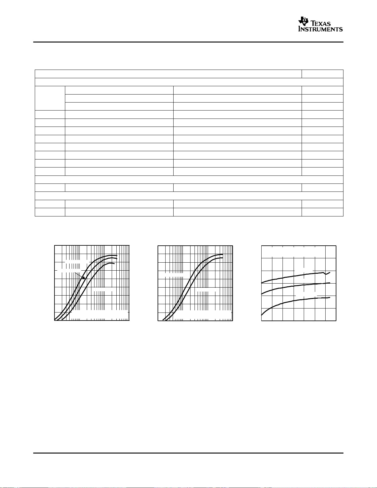
FIGURE
8
EFFICIENCY EFFICIENCY EFFICIENCY
vs vs vs
LOAD CURRENT LOAD CURRENT INPUT VOLTAGE
Figure 1. Figure 2. Figure 3.
Submit Documentation Feedback
www.ti.com
V
SW
10 V/div
V
O
50 mV/div
VI = 3.3 V
VO = 10 V/300 mA
I
L
1 A/div
250 ns/div
100
150
200
250
300
350
−40 −20 0 20 40 60 80 100
− N−Channel Main Switch − mΩ
TA − Free-Air Temperature − °C
Vo1 = 5 V
Vo1 = 15 V
Vo1 = 10 V
r
DS(on)
1.3
1.4
1.5
1.6
1.7
1.8
1.9
−40 −20 0 20 40 60 80 100
T
A
− Free-Air Temperature − °C
Switching Frequency − MHz
VI = 2.7 V
VI = 3.3 V
VI = 5.8 V
Vo1
200 mV/div
VI = 3.3 V
Vo1 = 10 V, CO= 22 µF
I
O
50 mA to 250 mA
100 µs/div
Vo1
100 mV/div
VI = 3.3 V
Vo1 = 10 V, CO= 2*22 µF
I
O
50 mA to 250 mA
100 µs/div
V
SW
10 V/div
V
O
50 mV/div
VI = 3.3 V
VO = 10 V/10 mA
I
L
500 mA/div
250 ns/div
Vo1
5 V/div
VI = 3.3 V
VO = 10 V,
IO = 300 mA
500 µs/div
I
I
500
mA/div
Vo1
5 V/div
VI = 3.3 V
VO = 10 V,
500 µs/div
Vo2
5 V/div
Vo3
10 V/div
0
0.02
0.04
0.06
0.08
0.10
0.12
0.14
0.16
0.18
0.20
8.8 9.8
10.8 11.8 12.8 13.8 14.8
Vo1 − Output Voltage − V
− Output Current − AI
O
Vo2 = −8 V
TA = −40°C
TA = 25°C
TA = 85°C
TPS65140 , TPS65141
TPS65145
SLVS497C – SEPTEMBER 2003 – REVISED APRIL 2006
SWITCHING FREQUENCY r
vs vs MODE
N-CHANNEL MAIN SWITCH PWM OPERATION CONTINUOUS
DS(on)
FREE-AIR TEMPERATURE FREE-AIR TEMPERATURE
Figure 4. Figure 5. Figure 6.
PWM OPERATION AT LIGHT LOAD LOAD TRANSIENT RESPONSE LOAD TRANSIENT RESPONSE
POWER-UP SEQUENCING SOFT START VO1 VO2 MAXIMUM LOAD CURRENT
Figure 7. Figure 8. Figure 9.
Figure 10. Figure 11. Figure 12.
Submit Documentation Feedback
9

www.ti.com
0
0.02
0.04
0.06
0.08
0.10
0.12
0.14
9
10 11 12 13 14 15
Vo1 − Output Voltage − V
− Output Current − AI
O
Vo3 = 18 V (Doubler Mode)
TA = 25°C
TA = 85°C
TA = −40°C
0
0.02
0.04
0.06
0.08
0.10
0.12
9
10 11 12 13 14 15
Vo1 − Output Voltage − V
− Output Current − AI
O
Vo3 = 28 V (Tripler Mode)
TA = 25°C
TA = 85°C
TA = −40°C
TPS65140 , TPS65141
TPS65145
SLVS497C – SEPTEMBER 2003 – REVISED APRIL 2006
VO3 MAXIMUM LOAD CURRENT VO3 MAXIMUM LOAD CURRENT
Figure 13. Figure 14.
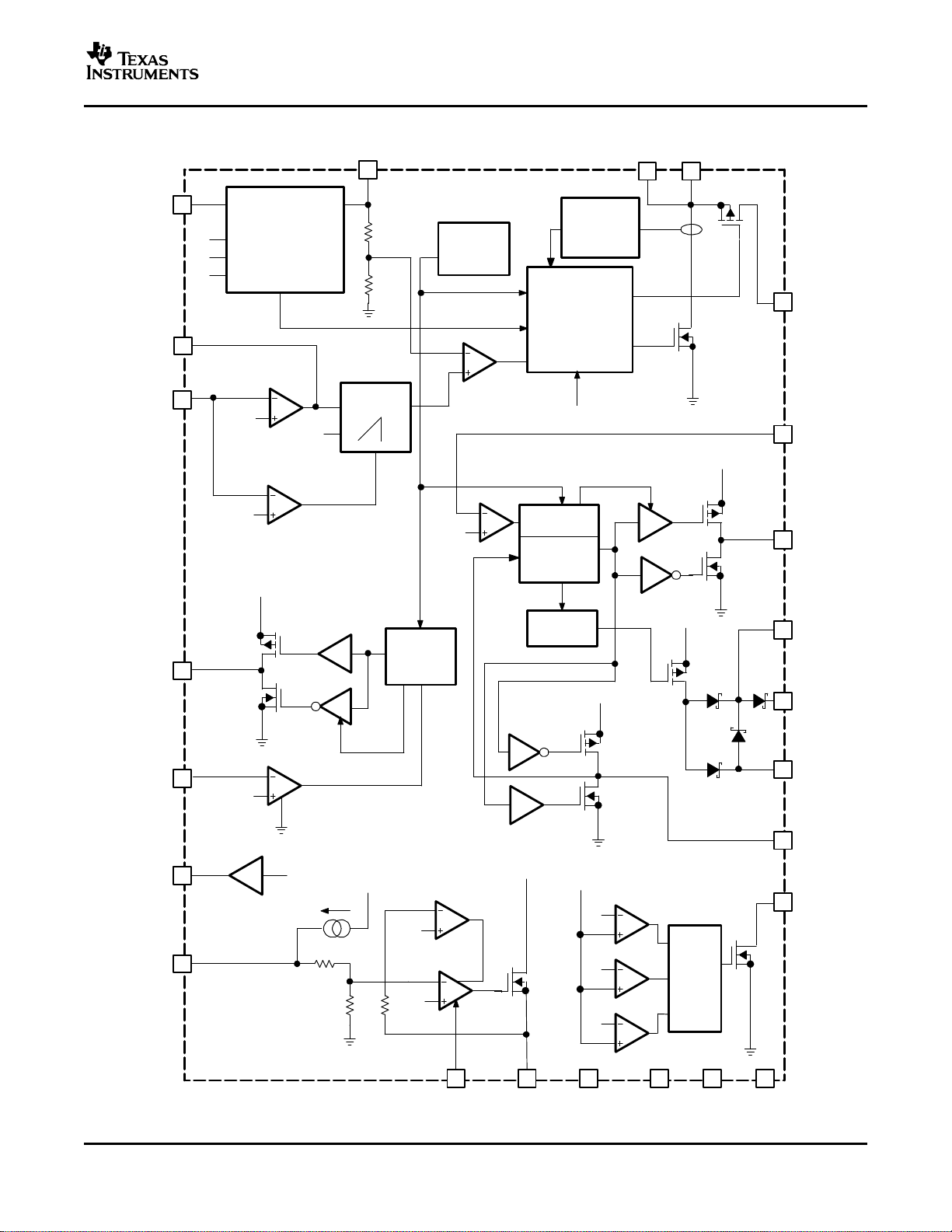
DETAILED DESCRIPTION
The TPS6514x series consists of a main boost converter operating with a fixed switching frequency of 1.6 MHz
to allow for small external components. The boost converter output voltage VO1 is also the input voltage,
connected via the pin SUP, for the positive and negative charge pump. The linear regulator controller is
independent from this system with its own enable pin. This allows the linear regulator controller to continue to
operate while the other supply rails are disabled or in shutdown due to a fault condition on one of their outputs.
Refer to the functional block diagram for more information.
Main Boost Converter
The main boost converter operates with PWM and a fixed switching frequency of 1.6 MHz. The converter uses a
unique fast response, voltage mode controller scheme with input voltage feedforward. This achieves excellent
line and load regulation (0.2% A load regulation typical) and allows the use of small external components. To
add higher flexibility to the selection of external component values, the device uses external loop compensation.
Although the boost converter looks like a nonsynchronous boost converter topology operating in discontinuous
mode at light load, the TPS6514x series maintains continuous conduction even at light load currents. This is
accoplished using the Virtual Synchronous Converter Technology for improved load transient response. This
architecture uses an external Schottky diode and an integrated MOSFET in parallel connected between SW and
SUP (see the functional block diagram). The integrated MOSFET Q2 allows the inductor current to become
negative at light load conditions. For this purpose, a small integrated P-channel MOSFET with typically 10 Ω
r
is sufficient. When the inductor current is positive, the external Schottky diode with the lower forward
DS(on)
voltage conducts the current. This causes the converter to operate with a fixed frequency in continuous
conduction mode over the entire load current range. This avoids the ringing on the switch pin as seen with a
standard nonsynchronous boost converter and allows a simpler compensation for the boost converter.
Power-Good Output
The TPS6514x sereis has an open-drain power-good output with a maximum sink capability of 1 mA. The
power-good output goes high as soon as the main boost converter VO1 and the negative and the positive charge
pumps are within regulation. The power-good output goes low as soon as one of the outputs is out of regulation.
In this case, the device goes into shutdown at the same time. See the electrical characteristics table for the
power-good thresholds.
Enable and Power-On Sequencing (EN, ENR)
The device has two enable pins. These pins should be terminated and not left floating to prevent faulty
operation. Pulling the enable pin (EN) high enables the device and starts the power-on sequencing with the main
boost converter VO1 coming up first, then the negative and positive charge pump. The linear regulator has an
independent enable pin (ENR). Pulling this pin low disables the regulator, and pulling this pin high enables this
regulator.
If the enable pin (EN) is pulled high, the device starts its power-on sequencing. The main boost converter starts
10
Submit Documentation Feedback

www.ti.com
TPS65140 , TPS65141
TPS65145
SLVS497C – SEPTEMBER 2003 – REVISED APRIL 2006
up first with its soft start. If the output voltage has reached 91.25% of its output voltage, the negative charge
pump comes up next. The negative charge pump starts with a soft start and when the output voltage has
reached 91% of the nominal value, the positive charge pump comes up with the soft start. Pulling the enable pin
low shuts down the device. Dependent on load current and output capacitance, each of the outputs comes
down.
Positive Charge Pump
The TPS6514x series has a fully regulated integrated positive charge pump generating VO3. The input voltage
for the charge pump is applied to the SUP pin that is equal to the output of the main boost converter VO1. The
charge pump is capable of supplying a minimum load current of 20 mA. Higher load currents are possible
depending on the voltage difference between VO1 and VO3. See Figure 13 and Figure 14 .
Negative Charge Pump
The TPS6514x sereis has a regulated negative charge pump using two external Schottky diodes. The input
voltage for the charge pump is applied to the SUP pin that is connected to the output of the main boost
converter VO1. The charge pump inverts the main boost converter output voltage and is capable of supplying a
minimum load current of 20 mA. Higher load currents are possible depending on the voltage difference between
VO1 and VO2. See Figure 12 .
Linear Regulator Controller
The TPS6514x series includes a linear regulator controller to generate a 3.3-V rail which is useful when the
system is powered from a 5-V supply. The regulator is independent from the other voltage rails of the device and
has its own enable (ENR). Since most of the systems require this voltage rail to come up first it is recommended
to use a R-C delay on EN. This delays the start-up of the main boost converter which reduces the inrush current
as well.
Soft Start
The main boost converter as well as the charge pumps and linear regulator have an internal soft start. This
avoids heavy voltage drops at the input voltage rail or at the output of the main boost converter VO1 during
start-up. See Figure 10 and Figure 11. During softstart of the main boost converter VO1 the internal current limit
threshold is increased in three steps. The device starts with the first step where the current limit is set to 2/5 of
the typical current limit (2/5 of 2.3A) for 1024 clock cycles then increased to 3/5 of the current limit for 1024 clock
cycles and the 3rd step is the full current limit. The TPS65141 has an extended softstart time where each step is
2048 clock cycles.
Fault Protection
All of the outputs of the TPS65140/45 have short-circuit detection and cause the device to go into shutdown.
The TPS65141, as an exception, does not enter shutdown in case one of the outputs falls below its power good
threshold. The main boost converter has overvoltage and undervoltage protection. If the output voltage VO1 rises
above the overvoltage protection threshold of typically 5% of VO1, then the device stops switching, but remains
operational. When the output voltage falls below this threshold, the converter continues operation. When the
output voltage falls below the undervoltage protection threshold of typically 8.75% of VO1, because of a
short-circuit condition, the TPS65140/45 goes into shutdown. Because there is a direct pass from the input to
the output through the diode, the short-circuit condition remains. If this condition needs to be avoided, a fuse at
the input or an output disconnect using a single transistor and resistor is required. The negative and positive
charge pumps have an undervoltage lockout (UVLO) to protect the LCD panel of possible latch-up conditions
due to a short-circuit condition or faulty operation. When the negative output voltage is typically above 9.5% of
its output voltage (closer to ground), then the device enters shutdown. When the positive charge pump output
voltage, VO3, is below 8% typical of its output voltage, the device goes into shutdown. See the fault protection
thresholds in the electrical characteristics table. The device is enabled by toggling the enable pin (EN) below 0.4
V or by cycling the input voltage below the UVLO of 1.7 V. The linear regulator reduces the output current to 20
mA typical under a short-circuit condition when the output voltage is typically < 1 V. See the functional block
diagram. The linear regulator does not go into shutdown under a short-circuit condition.
Submit Documentation Feedback
11

www.ti.com
TPS65140 , TPS65141
TPS65145
SLVS497C – SEPTEMBER 2003 – REVISED APRIL 2006
Thermal Shutdown
A thermal shutdown is implemented to prevent damage due to excessive heat and power dissipation. Typically,
the thermal shutdown threshold is 160 °C. If this temperature is reached, the device goes into shutdown. The
device can be enabled by toggling the enable pin to low and back to high or by cycling the input voltage to GND
and back to VIagain.
12
Submit Documentation Feedback

www.ti.com
D
V
out
VD V
in
V
out
VD V
sw
10 V 0.8 V 3.3 V
10 V 0.8 V 0.5 V
0.73
I
L
I
out
1 D
300 mA
1 0.73
1.11 A
i
L
Vin V
sw
D
fs L
(3.3 V 0.5 V) 0.73
1.6 MHz 4.2 H
304 mA
I
swpeak
I
L
i
L
2
1.11 A
304 mA
2
1.26 A
TPS65140 , TPS65141
SLVS497C – SEPTEMBER 2003 – REVISED APRIL 2006
APPLICATION INFORMATION
BOOST CONVERTER DESIGN PROCEDURE
The first step in the design procedure is to calculate the maximum possible output current of the main boost
converter under certain input and output voltage conditions. Below is an example for a 3.3-V to 10-V conversion:
V
= 3.3 V, V
in
1. Duty cycle:
2. Average inductor current:
3. Inductor peak-to-peak ripple current:
4. Peak switch current:
= 10 V, Switch voltage drop V
out
= 0.5 V, Schottky diode forward voltage V
sw
D
= 0.8 V
TPS65145
The integrated switch, the inductor, and the external Schottky diode must be able to handle the peak switch
current. The calculated peak switch current has to be equal or lower than the minimum N-MOSFET switch
current limit as specified in the electrical characteristics table (1.6 A for the TPS65140/41 and 0.96 A for the
TPS65145). If the peak switch current is higher, then the converter cannot support the required load current.
This calculation must be done for the minimum input voltage where the peak switch current is highest. The
calculation includes conduction losses like switch r
(0.5 V) and diode forward drop voltage losses (0.8 V).
DS(on)
Additional switching losses, inductor core and winding losses, etc., require a slightly higher peak switch current
in the actual application. The above calculation still allows for a good design and component selection.
Inductor Selection
Several inductors work with the TPS6514x. Especially with the external compensation, the performance can be
adjusted to the specific application requirements. The main parameter for the inductor selection is the saturation
current of the inductor which should be higher than the peak switch current as calculated above with additional
margin to cover for heavy load transients and extreme start-up conditions. Another method is to choose the
inductor with a saturation current at least as high as the minimum switch current limit of 1.6 A for the
TPS65140/41 and 0.96 A for the TPS65145. The different switch current limits allow selection of a physically
smaller inductor when less output current is required. The second important parameter is the inductor DC
resistance. Usually, the lower the DC resistance, the higher the efficiency. However, the inductor DC resistance
is not the only parameter determining the efficiency. Especially for a boost converter where the inductor is the
energy storage element, the type and material of the inductor influences the efficiency as well. Especially at high
switching frequencies of 1.6 MHz, inductor core losses, proximity effects, and skin effects become more
important. Usually, an inductor with a larger form factor yields higher efficiency. The efficiency difference
between different inductors can vary between 2% to 10%. For the TPS6514x, inductor values between 3.3 µ H
and 6.8 µ H are a good choice but other values can be used as well. Possible inductors are shown in Table 1 .
Submit Documentation Feedback
13

www.ti.com
V
out
I
out
C
out
1
f
s
Ip L
V
out
Vd V
in
Ip ESR
TPS65140 , TPS65141
TPS65145
SLVS497C – SEPTEMBER 2003 – REVISED APRIL 2006
APPLICATION INFORMATION (continued)
Table 1. Inductor Selection
DEVICE INDUCTOR VALUE COMPONENT SUPPLIER DIMENSIONS / mm ISAT/DCR
4.7 µ H Coilcraft DO1813P-472HC 8,89 x 6,1 x 5 2.6 A/54 m Ω
4.2 µ H Sumida CDRH5D28 4R2 5,7 x 5,7 x 3 2.2 A/23 m Ω
TPS65140
TPS65145 3.3 µ H Sumida CDRH2D18/HP 3R3 3,2 x 3,2 x 2 1.45 A/69 m Ω
Output Capacitor Selection
For best output voltage filtering, a low ESR output capacitor is recommended. Ceramic capacitors have a low
ESR value but depending on the application, tantalum capacitors can be used as well. A 22- µ F ceramic output
capacitor works for most of the applications. Higher capacitor values can be used to improve load transient
regulation. See Table 2 for the selection of the output capacitor. The output voltage ripple can be calculated as:
4.7 µ H Sumida CDC5D23 4R7 6 x 6 x 2,5 1.6 A/48 m Ω
3.3 µ H Wuerth Elektronik 744042003 4,8 x 4,8 x 2 1.8 A/65 m Ω
4.2 µ H Sumida CDRH6D12 4R2 6,5 x 6, 5 x 1,5 1.8 A/60 m Ω
3.3 µ H Sumida CDRH6D12 3R3 6,5 x 6,5 x 1,5 1.9 A/50 m Ω
3.3 µ H Sumida CDPH4D19 3R3 5,1 x 5,1 x 2 1.5 A/26 m Ω
3.3 µ H Coilcraft DO1606T-332 6,5 x 5,2 x 2 1.4 A/120 m Ω
4.7 µ H Wuerth Elektronik 744010004 5,5 x 3,5 x 1 1 A/260 m Ω
3.3 µ H Coilcraft LPO6610-332M 6,6 x 5,5 x 1 1.3 A/160 m Ω
with:
IP = Peak switch current as calculated in the previous section with I
SW(peak)
.
L = Selected inductor value
I
= Normal load current
OUT
fs= Switching frequency
Vd= Rectifier diode forward voltage (typical 0.3 V)
C
= Selected output capacitor
OUT
ESR = Output capacitor ESR value
Input Capacitor Selection
For good input voltage filtering, low ESR ceramic capacitors are recommended. A 22- µ F ceramic input capacitor
is sufficient for most of applications. For better input voltage filtering, this value can be increased. See Table 2
and the typical applications for input capacitor recommendations.
Table 2. Input and Output Capacitors Selection
CAPACITOR VOLTAGE RATING COMPONENT SUPPLIER COMMENTS
22 µ F/1210 16 V Taiyo Yuden EMK325BY226MM C
22 µ F/1206 6.3 V Taiyo Yuden JMK316BJ226 C
O
I
Rectifier Diode Selection
To achieve high efficiency, a Schottky diode should be used. The voltage rating should be higher than the
maximum output voltage of the converter. The average forward current should be equal to the average inductor
current of the converter. The main parameter influencing the efficiency of the converter is the forward voltage
and the reverse leakage current of the diode; both should be as low as possible. Possible diodes are: On
Semiconductor MBRM120L, Microsemi UPS120E, and Fairchild Semiconductor MBRS130L.
14
Submit Documentation Feedback

www.ti.com
V
out
1.146 V 1
R1
R2
SW
SW
FB1
SUP
C2+
C2−/MODE
D1
C8
6.8 pF
R1
430 kΩ
R2
56 kΩ
C4
22 µF
VO1
Up to 10 V/150 mA
C2 0.22 µF
C8
1
2 fz R1
1
2 50 kHz R1
TPS65140 , TPS65141
TPS65145
SLVS497C – SEPTEMBER 2003 – REVISED APRIL 2006
Converter Loop Design and Stability
The TPS6514x converter loop can be externally compensated and allows access to the internal
transconductance error amplifier output at the COMP pin. A small feedforward capacitor across the upper
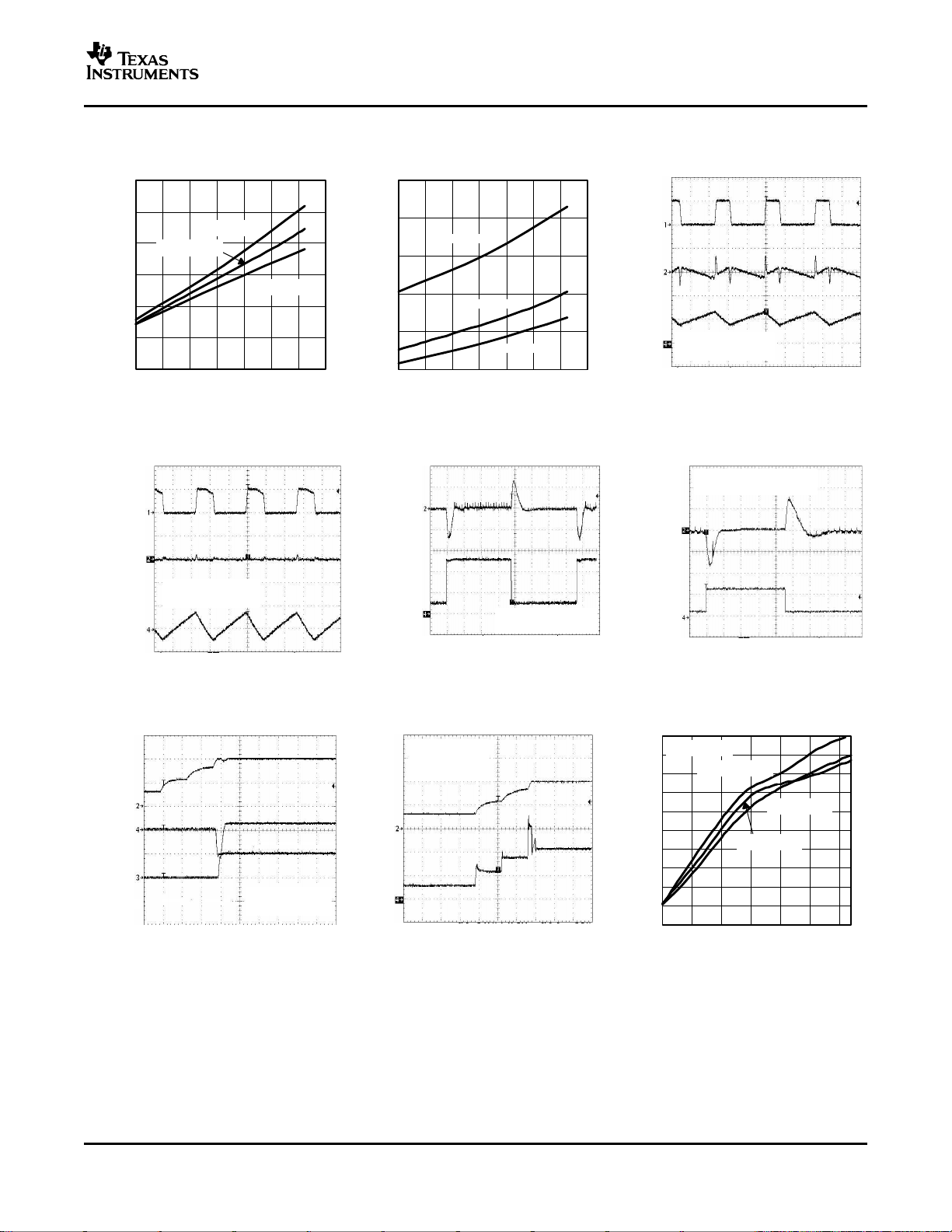
feedback resistor divider speeds up the circuit as well. To test the converter stability and load transient
performance of the converter, a load step from 50 mA to 250 mA is applied and the output voltage of the
converter is monitored. Applying load steps to the converter output is a good tool to judge the stability of such a
boost converter.
Design Procedure Quick Steps
1. Select the feedback resistor divider to set the output voltage.
2. Select the feedforward capacitor to place a zero at 50 kHz.
3. Select the compensation capacitor on pin COMP. The smaller the value, the higher the low frequency gain.
4. Use a 50-k Ω potentiometer in series to C
transient by adjusting the potentiometer. Select a resistor value that comes closest to the potentiometer
resistor value. This needs to be done at the highest V
critical at these conditions.
Setting the Output Voltage and Selecting the Feedforward Capacitor
The output voltage is set by the external resistor divider and is calculated as:
and monitor V
c
during load transients. Fine tune the load
out
and highest load current because stability is most
in
Across the upper resistor, a bypass capacitor is required to speed up the circuit during load transients as shown
in Figure 15 .
Figure 15. Feedforward Capacitor
Together with R1 the bypass capacitor C8 sets a zero in the control loop at approximately 50 kHz:
A value closest to the calculated value should be used. Larger feedforward capacitor values reduce the load
regulation of the converter and cause load steps as shown in Figure 16 .
Submit Documentation Feedback
15

www.ti.com
Load Step
VIN
COMP
R
C
15 kΩ
C
C
1 nF
f
z
1
2 Cc Rc
CC = 4.7 nF
TPS65140 , TPS65141
TPS65145
SLVS497C – SEPTEMBER 2003 – REVISED APRIL 2006
Figure 16. Load Step Caused By A Too Large Feedforward Capacitor Value
Compensation
The regulator loop can be compensated by adjusting the external components connected to the COMP pin. The
COMP pin is connected to the output of the internal transconductance error amplifier. A typical compensation
scheme is shown in Figure 17 .
Figure 17. Compensation Network
The compensation capacitor C
adjusts the low frequency gain, and the resistor value adjusts the high frequency
c
gain. The following formula calculates at what frequency the resistor increases the high frequency gain.
Lower input voltages require a higher gain and a lower compensation capacitor value. A good start is C
for a 3.3-V input and C
= 2.2 nF for a 5-V input. If the device operates over the entire input voltage range from
c
2.7 V to 5.8 V, a larger compensation capacitor up to 10 nF is recommended. Figure 18 shows the load transient
with a larger compensation capacitor, and Figure 19 shows a smaller compensation capacitor.
Figure 18. C
C
= 4. 7 nF
= 1 nF
c
16
Submit Documentation Feedback

www.ti.com
CC = 1 nF
TPS65140 , TPS65141
TPS65145
SLVS497C – SEPTEMBER 2003 – REVISED APRIL 2006
Figure 19. C
Lastly, R
needs to be selected. A good practice is to use a 50-k Ω potentiometer and adjust the potentiometer
c
for the best load transient where no oscillations should occur. These tests have to be done at the highest V
= 1 nF
C
and
in
highest load current because the converter stability is most critical under these conditions. Figure 20 , Figure 21 ,
and Figure 22 show the fine tuning of the loop with Rc.
Figure 20. Overcompensated (Damped Oscillation), R
Is Too Large
C
Figure 21. Undercompensated (Loop Is Too Slow), R
Submit Documentation Feedback
Is Too Small
C
17

www.ti.com
V = -V x
OUT REF
= -1.213 V x
RR3
3
RR4
4
R3 = R4 x
= R4 x
|V
OUT
|
|V
OUT
|
V
REF
1.213
TPS65140 , TPS65141
TPS65145
SLVS497C – SEPTEMBER 2003 – REVISED APRIL 2006
Figure 22. Optimum, R
Is Ideal
C
Negative Charge Pump
The negative charge pump provides a regulated output voltage by inverting the main output voltage, VO1. The
negative charge pump output voltage is set with external feedback resistors.
The maximum load current of the negative charge pump depends on the voltage drop across the external
Schottky diodes, the internal on resistance of the charge pump MOSFETS Q8 and Q9, and the impedance of
the flying capacitor, C12. When the voltage drop across these components is larger than the voltage difference
from VO1 to VO2, the charge pump is in drop out, providing the maximum possible output current. Therefore, the
higher the voltage difference between VO1 and VO2, the higher the possible load current. See Figure 12 for the
possible output current versus boost converter voltage VO1 and the calculations below.
Vout
= -(V
min
O
1 - 2 V
- IO(2 x r
D
DS(on)Q8
+ 2 x r
DS(on)Q9
+ X
))
cfly
Setting the output voltage:
The lower feedback resistor value, R4, should be in a range between 40 k Ω to 120 k Ω or the overall feedback
resistance should be within 500 k Ω to 1 M Ω . Smaller values load the reference too heavy and larger values may
cause stability problems. The negative charge pump requires two external Schottky diodes. The peak current
rating of the Schottky diode has to be twice the load current of the output. For a 20 mA output current, the dual
Schottky diode BAT54 or similar is a good choice.
Positive Charge Pump
The positive charge pump can be operated in a voltage doubler mode or a voltage tripler mode depending on
the configuration of the C2+ and C2-/MODE pins. Leaving the C2+ pin open and connecting C2-/MODE to GND
forces the positive charge pump to operate in a voltage doubler mode. If higher output voltages are required the
positive charge pump can be operated as a voltage tripler. To operate the charge pump in the voltage tripler
mode, a flying capacitor needs to be connected to C2+ and C2-/MODE.
The maximum load current of the positive charge pump depends on the voltage drop across the internal
Schottky diodes, the internal on-resistance of the charge pump MOSFETS, and the impedance of the flying
capacitor. When the voltage drop across these components is larger than the voltage difference VO1 x 2 to VO3
(doubler mode) or VO1 x 3 to VO3 (tripler mode), then the charge pump is in dropout, providing the maximum
possible output current. Therefore, the higher the voltage difference between VO1 x 2 (doubler) or VO1 x 3
(tripler) to VO3, the higher the possible load current. See Figure 13 and Figure 14 for output current versus boost
converter voltage, VO1, and the following calculations.
Voltage doubler:
Voltage tripler:
18
VO3
VO3
= 2 x VO1 - (2 V
max
= 3 x V
max
- (3 x V
O
+ 2 x IOx (2 x r
D
D
+ 2 x IOx (3 x r
DS(on)Q5
DS(on)Q5
Submit Documentation Feedback
+ r
DS(on)Q3
+ r
DS(on)Q3
+ r
DS(on)Q4
+ r
DS(on)Q4
+ X
))
C1
+ X
+ X
C1
))
C2

www.ti.com
V
out
1.214 1
R5
R6
R5 R6
V
out
V
FB
1
R6
V
out
1.214
1
TPS65140 , TPS65141
TPS65145
SLVS497C – SEPTEMBER 2003 – REVISED APRIL 2006
The output voltage is set by the external resistor divider and is calculated as:
Linear Regulator Controller
The TPS6514x includes a linear regulator controller to generate a 3.3-V rail when the system is powered from a
5-V supply. Because an external npn transistor is required, the input voltage of the TPS6514x applied to VIN
needs to be higher than the output voltage of the regulator. To provide a minimum base drive current of 13.5
mA, a minimum internal voltage drop of 500 mV from V
minimum input voltage on VIN for a certain output voltage as the following calculation shows:
V
= VO4 + V
I(min)
The base drive current together with the h
Using a standard npn transistor like the BCP68 allows an output current of 1 A and using the BCP54 allows a
load current of 337 mA for an input voltage of 5 V. Other transistors can be used as well, depending on the
required output current, power dissipation, and PCB space. The device is stable with a 4.7- µ F ceramic output
capacitor. Larger output capacitor values can be used to improve the load transient response when higher load
currents are required.
+ 0.5 V
BE
of the external transistor determines the possible output current.
FE
to V
in
is required. This can be translated into a
base
Thermal Information
An influential component of the thermal performance of a package is board design. To take full advantage of the
heat dissipation abilities of the PowerPAD or QFN package with exposed thermal die, a board that acts similar to
a heatsink and allows for the use of an exposed (and solderable) deep downset pad should be used. For further
information. see Texas Instrumens application notes (SLMA002) PowerPAD Thermally Enhanced Package, and
(SLMA004) Power Pad Made Easy. For the QFN package, see the application report (SLUA271) QFN/SON
PCB Attachement. Especially for the QFN package it is required to solder down the Thermal Pad to achieve the
required thermal resistance.
Layout Considerations
For all switching power supplies, the layout is an important step in the design, especially at high-peak currents
and switching frequencies. If the layout is not carefully designed, the regulator might show stability and EMI
problems. Therefore, the traces carrying high-switching currents should be routed first using wide and short
traces. The input filter capacitor should be placed as close as possible to the input pin VIN of the IC. See the
evaluation module (EVM) for a layout example.
Submit Documentation Feedback
19

www.ti.com
VIN
COMP
GND
EN
ENR
C1+
C1−
DRV
FB2
REF
FB4
BASE
SW
SW
FB1
SUP
C2+
C2−/MODE
OUT3
FB3
PG
PGND
PGND
GND
TPS65140
D1
L1
3.3uH
C3
22uF
Vin
3.3V
Vo1
10V / 150 mA
Vo3
up to 23V/20mA
System Power
Good
C7
0.22u
R7
33k
D2
D3
C1
0.22u
R3
620k
R4
150k
C11
220nF
C6
0.22u
R5
1M
R6
56k
C4
22uF
C2
0.22u
C5
6.8pF
R2
56k
R1
430
C12 0.22u
C13
1n
Vin
R7
15k
Vo2
−5 V / 20 mA
VIN
COMP
GND
EN
ENR
C1+
C1−
DRV
FB2
REF
FB4
BASE
SW
SW
FB1
SUP
C2+
C2−/MODE
OUT3
FB3
PG
PGND
PGND
GND
TPS65140
D1
L1
4.7uH
C3
22uF
Vin
5.0 V
Vo1
13.5V / 400 mA
Vo3
up to 23V/20mA
System Power
Good
C7
0.22u
R7
33k
C10
4.7uF
Q1
BCP68
Vo4
3.3V/500mA
Vin
D2
D3
C1
0.22u
R3
750k
R4
130k
C11
220nF
C6
0.22u
C9
1uF
R5
1M
R6
56k
C4
22uF
C5
3.3pF
R2
75k
R1
820
C12 0.22u
C13
2.2n
Vin
R7
4.3k
Vo2
−7 V / 20 mA
TPS65140 , TPS65141
TPS65145
SLVS497C – SEPTEMBER 2003 – REVISED APRIL 2006
20
Figure 23. Typical Application, Notebook Supply
Figure 24. Typical Application, Monitor Supply
Submit Documentation Feedback
PACKAGE OPTION ADDENDUM
www.ti.com
14-Aug-2006
PACKAGING INFORMATION
Orderable Device Status
(1)
Package
Type
Package
Drawing
Pins Package
Qty
Eco Plan
TPS65140PWP ACTIVE HTSSOP PWP 24 60 Green (RoHS &
no Sb/Br)
TPS65140PWPG4 ACTIVE HTSSOP PWP 24 60 Green (RoHS &
no Sb/Br)
TPS65140PWPR ACTIVE HTSSOP PWP 24 2000 Green (RoHS &
no Sb/Br)
TPS65140PWPRG4 ACTIVE HTSSOP PWP 24 2000 Green (RoHS &
no Sb/Br)
TPS65140RGER ACTIVE QFN RGE 24 3000 Green (RoHS &
no Sb/Br)
TPS65140RGERG4 ACTIVE QFN RGE 24 3000 Green (RoHS &
no Sb/Br)
TPS65141PWP ACTIVE HTSSOP PWP 24 60 Green (RoHS &
no Sb/Br)
TPS65141PWPG4 ACTIVE HTSSOP PWP 24 60 Green (RoHS &
no Sb/Br)
TPS65141PWPR ACTIVE HTSSOP PWP 24 2000 Green (RoHS &
no Sb/Br)
TPS65141PWPRG4 ACTIVE HTSSOP PWP 24 2000 Green (RoHS &
no Sb/Br)
TPS65141RGER ACTIVE QFN RGE 24 3000 Green (RoHS &
no Sb/Br)
TPS65141RGERG4 ACTIVE QFN RGE 24 3000 Green (RoHS &
no Sb/Br)
TPS65145PWP ACTIVE HTSSOP PWP 24 60 Green (RoHS &
no Sb/Br)
TPS65145PWPG4 ACTIVE HTSSOP PWP 24 60 Green (RoHS &
no Sb/Br)
TPS65145PWPR ACTIVE HTSSOP PWP 24 2000 Green (RoHS &
no Sb/Br)
TPS65145PWPRG4 ACTIVE HTSSOP PWP 24 2000 Green (RoHS &
no Sb/Br)
TPS65145RGER ACTIVE QFN RGE 24 3000 Green (RoHS &
no Sb/Br)
TPS65145RGERG4 ACTIVE QFN RGE 24 3000 Green (RoHS &
no Sb/Br)
(1)
The marketing status values are defined as follows:
ACTIVE: Product device recommended for new designs.
LIFEBUY: TI has announced that the device will be discontinued, and a lifetime-buy period is in effect.
NRND: Not recommended for new designs. Device is in production to support existing customers, but TI does not recommend using this part in
a new design.
PREVIEW: Device has been announced but is not in production. Samples may or may not be available.
OBSOLETE: TI has discontinued the production of the device.
(2)
Lead/Ball Finish MSL Peak Temp
CU NIPDAU Level-2-260C-1 YEAR
CU NIPDAU Level-2-260C-1 YEAR
CU NIPDAU Level-2-260C-1 YEAR
CU NIPDAU Level-2-260C-1 YEAR
Call TI Level-2-260C-1 YEAR
Call TI Level-2-260C-1 YEAR
CU NIPDAU Level-2-260C-1 YEAR
CU NIPDAU Level-2-260C-1 YEAR
CU NIPDAU Level-2-260C-1 YEAR
CU NIPDAU Level-2-260C-1 YEAR
CU NIPDAU Level-2-260C-1 YEAR
CU NIPDAU Level-2-260C-1 YEAR
CU NIPDAU Level-2-260C-1 YEAR
CU NIPDAU Level-2-260C-1 YEAR
CU NIPDAU Level-2-260C-1 YEAR
CU NIPDAU Level-2-260C-1 YEAR
Call TI Level-2-260C-1 YEAR
Call TI Level-2-260C-1 YEAR
(3)
(2)
Eco Plan - The planned eco-friendly classification: Pb-Free (RoHS), Pb-Free (RoHS Exempt), or Green (RoHS & no Sb/Br) - please check
http://www.ti.com/productcontent for the latest availability information and additional product content details.
TBD: The Pb-Free/Green conversion plan has not been defined.
Pb-Free (RoHS): TI's terms "Lead-Free" or "Pb-Free" mean semiconductor products that are compatible with the current RoHS requirements
for all 6 substances, including the requirement that lead not exceed 0.1% by weight in homogeneous materials. Where designed to be soldered
at high temperatures, TI Pb-Free products are suitable for use in specified lead-free processes.
Pb-Free (RoHS Exempt): This component has a RoHS exemption for either 1) lead-based flip-chip solder bumps used between the die and
Addendum-Page 1

PACKAGE OPTION ADDENDUM
www.ti.com
package, or 2) lead-based die adhesive used between the die and leadframe. The component is otherwise considered Pb-Free (RoHS
compatible) as defined above.
Green (RoHS & no Sb/Br): TI defines "Green" to mean Pb-Free (RoHS compatible), and free of Bromine (Br) and Antimony (Sb) based flame
retardants (Br or Sb do not exceed 0.1% by weight in homogeneous material)
(3)
MSL, Peak Temp. -- The Moisture Sensitivity Level rating according to the JEDEC industry standard classifications, and peak solder
temperature.
Important Information and Disclaimer:The information provided on this page represents TI's knowledge and belief as of the date that it is
provided. TI bases its knowledge and belief on information provided by third parties, and makes no representation or warranty as to the
accuracy of such information. Efforts are underway to better integrate information from third parties. TI has taken and continues to take
reasonable steps to provide representative and accurate information but may not have conducted destructive testing or chemical analysis on
incoming materials and chemicals. TI and TI suppliers consider certain information to be proprietary, and thus CAS numbers and other limited
information may not be available for release.
In no event shall TI's liability arising out of such information exceed the total purchase price of the TI part(s) at issue in this document sold by TI
to Customer on an annual basis.
14-Aug-2006
Addendum-Page 2


IMPORTANT NOTICE
Texas Instruments Incorporated and its subsidiaries (TI) reserve the right to make corrections, modifications,
enhancements, improvements, and other changes to its products and services at any time and to discontinue
any product or service without notice. Customers should obtain the latest relevant information before placing
orders and should verify that such information is current and complete. All products are sold subject to TI’s terms
and conditions of sale supplied at the time of order acknowledgment.
TI warrants performance of its hardware products to the specifications applicable at the time of sale in
accordance with TI’s standard warranty. Testing and other quality control techniques are used to the extent TI
deems necessary to support this warranty . Except where mandated by government requirements, testing of all
parameters of each product is not necessarily performed.
TI assumes no liability for applications assistance or customer product design. Customers are responsible for
their products and applications using TI components. To minimize the risks associated with customer products
and applications, customers should provide adequate design and operating safeguards.
TI does not warrant or represent that any license, either express or implied, is granted under any TI patent right,
copyright, mask work right, or other TI intellectual property right relating to any combination, machine, or process
in which TI products or services are used. Information published by TI regarding third-party products or services
does not constitute a license from TI to use such products or services or a warranty or endorsement thereof.
Use of such information may require a license from a third party under the patents or other intellectual property
of the third party, or a license from TI under the patents or other intellectual property of TI.
Reproduction of information in TI data books or data sheets is permissible only if reproduction is without
alteration and is accompanied by all associated warranties, conditions, limitations, and notices. Reproduction
of this information with alteration is an unfair and deceptive business practice. TI is not responsible or liable for
such altered documentation.
Resale of TI products or services with statements different from or beyond the parameters stated by TI for that
product or service voids all express and any implied warranties for the associated TI product or service and
is an unfair and deceptive business practice. TI is not responsible or liable for any such statements.
Following are URLs where you can obtain information on other Texas Instruments products and application
solutions:
Products Applications
Amplifiers amplifier.ti.com Audio www.ti.com/audio
Data Converters dataconverter.ti.com Automotive www.ti.com/automotive
DSP dsp.ti.com Broadband www.ti.com/broadband
Interface interface.ti.com Digital Control www.ti.com/digitalcontrol
Logic logic.ti.com Military www.ti.com/military
Power Mgmt power.ti.com Optical Networking www.ti.com/opticalnetwork
Microcontrollers microcontroller.ti.com Security www.ti.com/security
Low Power Wireless www.ti.com/lpw Telephony www.ti.com/telephony
Video & Imaging www.ti.com/video
Wireless www.ti.com/wireless
Mailing Address: Texas Instruments
Post Office Box 655303 Dallas, Texas 75265
Copyright 2006, Texas Instruments Incorporated
 Loading...