

Page 1
CONDITION
TPS5100
TRIPLE-CHANNEL PWM CONTROL CIRCUITS
SLVS169 – JANUARY 2000
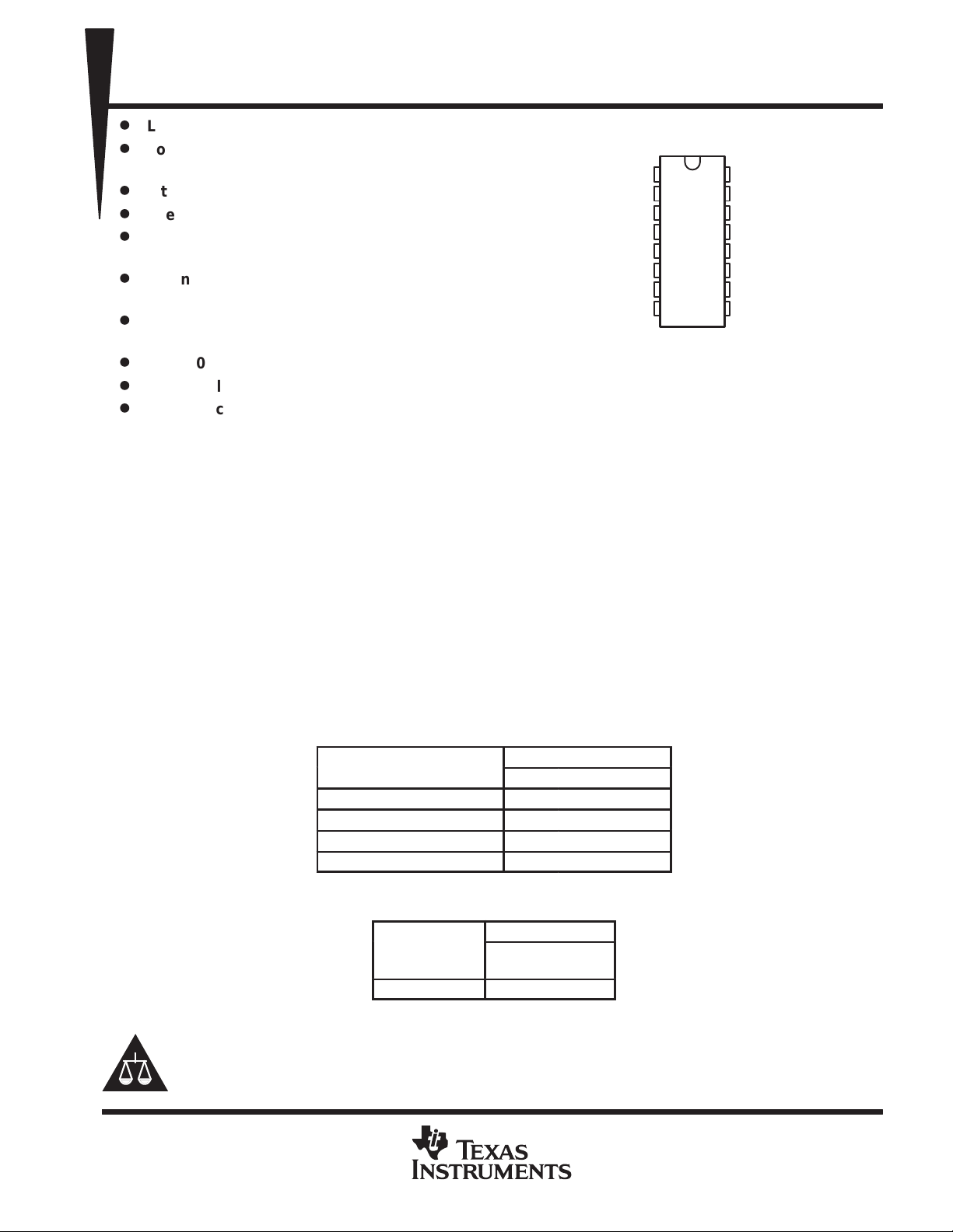
IN-2
E/O2
V
CC
OUT2
OUT3
OUT1
GND
SCP
PW PACKAGE
(TOP VIEW)
1
16
2
15
3
14
4
13
5
12
6
11
7
10
8
9
E/O3
IN-3
IN-1
E/O1
C
T/RT
DTC2
DTC1/3
V
REF
D
Low Voltage Operation . . . 2.5 V to 7 V
D
Low Power . . . 3. 5 mA
(f = 500 kHz, Duty = 50%)
D
Internal Undervoltage Lockout Protection
D
Internal Short Circuit Protection
D
Wide Operating Frequency . . . 50 kHz to
1 MHz
D
Internal Precision Reference . . . 1.25 V ±1%
(25°C)
D
On/Off Switch for CH1/3 Pair and Ch2 (see
Function Table)
D
0 to 100% Dead Time Control
D
Totem Pole Output Stage
D
Smal l Package . . . 16 Pin TSSOP
description
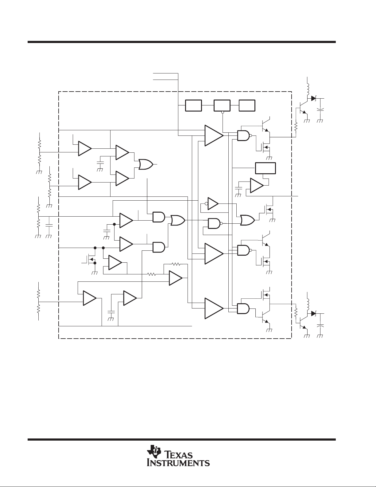
The TPS5100 is a triple PWM control circuit, primarily designed to compose the power supply for LCD display .
Each PWM channel has own error amplifier, PWM comparator, dead-time control and output driver. The
trimmed voltage reference, oscillator, undervoltage lockout and short circuit protection are common for all
channels.
This device includes two boost exclusive circuits (ch1,3) and a buck-boost exclusive circuit (ch2). The operating
frequency is set with external resister and capacitor, and dead time is continuously adjustable form 0% to 100%
duty cycle with resistive divider network. Soft start function can be implemented by adding a capacitor to dead
time divider network. Two dead time control inputs are assigned for ch1,3 pair and ch2 individually and each
dead time control input can be used to control on/off operation. TPS5100 can operate from 2.5 V supply voltage
and ch1,3 pair and ch2 operate with reverse phase switching each other to achieve efficient operation in low
power and battery powered system.
The TPS5100 is characterized for operation from –20°C to 85°C.
FUNCTION TABLE
DTC1/3 >. 0.3 V, DTC2 > 0.3 V ON H ON L ON H
DTC1/3 > 0.3 V, DTC2 <. 0.2 V ON H OFF H ON H
DTC1/3 < 0.2 V, DTC2 > 0.3 V OFF L ON L OFF L
DTC1/3 < 0.2 V, DTC2 < 0.2 V OFF L OFF H OFF L
AVAILABLE OPTIONS
T
A
–20°C to 85°C TPS5100PW
Please be aware that an important notice concerning availability, standard warranty, and use in critical applications of
Texas Instruments semiconductor products and disclaimers thereto appears at the end of this data sheet.
PRODUCTION DATA information is current as of publication date.
Products conform to specifications per the terms of Texas Instruments
standard warranty. Production processing does not necessarily include
testing of all parameters.
OUTPUT
CH-1 CH-2 CH-3
PACKAGE
TSSOP
(PW)
Copyright 2000, Texas Instruments Incorporated
POST OFFICE BOX 655303 • DALLAS, TEXAS 75265
1
Page 2
TPS5100
TRIPLE-CHANNEL PWM CONTROL CIRCUITS
SLVS169 – JANUARY 2000
functional block diagram
+
_
+
_
+
–
+
+
_
+
_
–
+
+
_
–
+
+
_
–
+
+
_
+
–
+
–
+
–
–
+
2
POST OFFICE BOX 655303 • DALLAS, TEXAS 75265
Page 3
Input threshold voltage
V
Input bias current
nA
Input threshold voltage (DTC1/3) (see Note 3)
f
500 kH
V
Input threshold voltage (DTC2) (see NOte 3)
f
500 kH
V
TPS5100
TRIPLE-CHANNEL PWM CONTROL CIRCUITS
SLVS169 – JANUARY 2000
electrical characteristics over recommended operating free-air temperature range, VCC = 3.3 V
(unless otherwise noted) (see Note 1)
PARAMETER TEST CONDITIONS MIN TYP MAX UNIT
V
REF
V
REF(dev)
R
EGIN
R
EGL
I
OS
NOTES: 1. Typical values of all parameters except for V
undervoltage lockout section
V
TH
V
TL
V
hys
NOTE 1: Typical values of all parameters except for V
protection control section
I
SCP
V
T2
V
T3
V
R
V
T5
NOTE 1: Typical values of all parameters except for V
oscillator section
f
OSC
f
dV
f
dT
I
CT/RT
V
OSCH
V
OSCL
NOTE 1: Typical values of all parameters except for V
dead time control section
I
BDT1/3
I
BDT2
V
T1
V
T0(DTC1/3)
V
T100(DTC1/3)
V
T0(DTC2)
V
T100(DTC2)
NOTES: 1: Typical values of all parameters except for V
Reference voltage I
Reference voltage change with T
Input regulation I
Output regulation I
Short-circuit output current V
2. The deviation parameter V
recommended free-air temperature range (–20°C to 85°C).
PARAMETER TEST CONDITIONS MIN TYP MAX UNIT
Upper threshold voltage TA = 25°C 2.2 2.3 2.4 V
Lower threshold voltage TA = 25°C 2 2.1 2.2 V
Hysteresis (VTH – VTL) TA = 25°C 0.1 0.2 0.3 V
PARAMETER TEST CONDITIONS MIN TYP MAX UNIT
Input terminal source current –1.4 –2 –2.6 µA
p
Latch reset threshold voltage TA = 25°C 0.8 1.5 V
Threshold voltage 1.20 1.25 1.30 V
PARAMETER TEST CONDITIONS MIN TYP MAX UNIT
Frequency CT = 130 pF, RT = 7 kΩ 400 500 600 kHz
Frequency change with V
Frequency change with T
Output source current –180 –200 –220 µA
H level output voltage 0.95 1 1.05 V
L level output voltage 0.35 0.40 0.45 V
PARAMETER TEST CONDITIONS MIN TYP MAX UNIT
p
Comparator threshold voltage 0.2 0.25 0.3 V
p
p
3. These specifications are not production tested. They are specified as ensured values on circuit design.
CC
A
A
REF(dev)
REF(dev)
is defined as the difference between the maximum and minimum values obtained over the
REF(dev)
REF(dev)
REF(dev)
REF(dev)
= –1 mA, TA = 25°C 1.237 1.250 1.263 V
REF
I
= –1 mA, See Note 2 15 25 mV
REF
= –1 mA, VCC = 2.5 V to 7 V 2 5 mV
REF
= –0.1 mA to –1 mA 1 5 mV
REF
= 0 –2 –10 –30 mA
REF
and fdT are specified at TA = 25°C.
and fdT are specified at TA = 25°C.
CH-1, 3 1.10 1.15 1.20
CH-2 0.20 0.25 0.30
and fdT are specified at TA = 25°C.
VCC = 2.5 V,
CT = 130 pF,
CT = 130 pF, RT = 7 kΩ 5% 10%
and fdT are specified at TA = 25°C.
V
V
Duty = 0%
Duty = 100%
Duty = 0%
Duty = 100%
and fdT are specified at TA = 25°C.
= 0.35 V to 1.05 V 200
DTC1/3
= 0.35 V to 1.05 V ±2 ±20
DTC2
OSC
OSC
TA = 25°C,
RT = 7 kΩ
=
=
0.3 0.4 0.5
z
0.9 1 1.1
0.3 0.4 0.5
z
0.9 1 1.1
1% 2%
POST OFFICE BOX 655303 • DALLAS, TEXAS 75265
3
Page 4
TPS5100
IIBInput bias current
nA
VIRInput voltage range
V
Output voltage swing
V
V
V
VT4Input bias voltage
mV
VOHHigh-level output voltage
V
VOLLow-level output voltage
V
TRIPLE-CHANNEL PWM CONTROL CIRCUITS
SLVS169 – JANUARY 2000
electrical characteristics over recommended operating free-air temperature range, VCC = 3.3 V
(unless otherwise noted) (see Note 1) (continued)
error amplifier section
PARAMETER TEST CONDITIONS MIN TYP MAX UNIT
V
IO
A
VD
B
1
V
OM+
V
OM–
I
OM+
I
OM–
NOTE 1: Typical values of all parameters except for V
output section
t
r
t
f
NOTE 1: Typical values of all parameters except for V
total device
I
CC
I
CCA
NOTE 1: Typical values of all parameters except for V
Input offset voltage CH1, 3, Av = 1 15 mV
p
p
Open-loop voltage amplification RFB = 200 kΩ 60 dB
Unity-gain bandwidth 1 MHz
p
Output sink current VID = 0.1 V, VO = 0.2 V 0.2 1 mA
Output source current VID = 0.1 V, VO = 1.2 V –60 –100 µA
p
REF(dev)
PARAMETER TEST CONDITIONS MIN TYP MAX UNIT
p
p
Rise time CL = 1000 pF 130 ns
Fall time IO = 1000 pF 50 ns
REF(dev)
PARAMETER TEST CONDITIONS MIN TYP MAX UNIT
Supply current Output OFF state 2.5 4 mA
Average supply current F
REF(dev)
CH1, 3, VI = –.95 V to 1.55 V ±10 ±20
CH2, VI = 0.4 V to 1 V ±10 ±20
CH1, 3, 0.95 1.55
CH2 0.4 1
= 0.1
ID
CH2, AV = 1, TA = 25°C 678 700 722
CH2, AV = 1 665 700 735
and fdT are specified at TA = 25°C.
and fdT are specified at TA = 25°C.
= 500 kHz, Duty = 50%, No load 3.5 5 mA
OSC
and fdT are specified at TA = 25°C.
IO = 60 µA 1.2
IO = 0.2 mA 0.2
IO = 20 mA (CH2) 2.9 3.05
IO = –40 mA (CH1, 3) 1.9 2.2 2.6
IO = 20 mA (CH1, 3) 0.2 0.4
IO = 40 mA (CH2) 0.2 0.3 0.6
4
POST OFFICE BOX 655303 • DALLAS, TEXAS 75265
Page 5
TPS5100
TRIPLE-CHANNEL PWM CONTROL CIRCUITS
SLVS169 – JANUARY 2000
TYPICAL CHARACTERISTICS
REFERENCE VOLTAGE
vs
FREE-AIR TEMPERATURE
1.27
VCC = 3.3 V
IO = –1 mA
1.26
1.25
1.24
– Reference Voltage – V
ref
V
1.23
1.22
–50 0 100 150
TA – Free-Air Temperature – °C
50
Figure 1
SUPPLY CURRENT
vs
FREE-AIR TEMPERATURE
5
VCC = 3.3 V
INPUT THRESHOLD VOLTAGE (UVLO)
vs
FREE-AIR TEMPERATURE
2.5
VCC = 3.3 V
2.4
2.3
2.2
2.1
– Input Threshold Voltage (UVLO) – V
IT
V
2
–50 0 100 150
TA – Free-Air Temperature – °C
50
Figure 2
SOURCE CURRENT
vs
FREE-AIR TEMPERATURE
–1.8
VCC = 3.3 V
4
I
CC
3
I
CCA
2
– Supply Current – mA
CC
I
1
0
–50 0 100 150
TA – Free-Air Temperature – °C
50
Figure 3
–2
Aµ
–2.2
S
I – Source Current –
–2.4
–2.6
–50 0 100 150
TA – Free-Air Temperature – °C
50
Figure 4
POST OFFICE BOX 655303 • DALLAS, TEXAS 75265
5
Page 6

TPS5100
TRIPLE-CHANNEL PWM CONTROL CIRCUITS
SLVS169 – JANUARY 2000
TYPICAL CHARACTERISTICS
OSCILLATOR FREQUENCY
vs
TIMING CAPACITOR
10k
VCC = 3.3 V
RT = 6.8 kΩ
TA = 25°C
1k
100
– Oscillator Frequency – kHz
OSC
f
10
10 100 10000
CT – Timing Capacitor – pF
1000
Figure 5
–190
VCC = 3.3 V
505
500
495
490
– Oscillator Frequency – kHz
485
OSC
f
480
–50 0 100 150
SOURCE CURRENT
vs
FREE-AIR TEMPERATURE
OSCILLATOR FREQUENCY
vs
FREE-AIR TEMPERATURE
VCC = 3.3 V
RT = 6.8 kΩ
CT = 130 pF
50
TA – Free-Air Temperature – °C
Figure 6
–195
Aµ
ICT/I
RT
–200
S
I – Source Current –
–205
–210
–50 0 100 150
TA – Free-Air Temperature – °C
50
Figure 7
6
POST OFFICE BOX 655303 • DALLAS, TEXAS 75265
Page 7

TPS5100
TRIPLE-CHANNEL PWM CONTROL CIRCUITS
SLVS169 – JANUARY 2000
7
Page 8

TPS5100
TRIPLE-CHANNEL PWM CONTROL CIRCUITS
SLVS169 – JANUARY 2000
TYPICAL CHARACTERISTICS
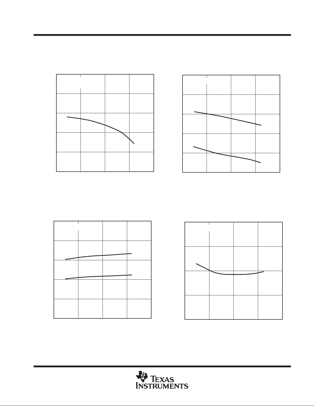
MAXIMUM PEAK OUTPUT VOLTAGE
vs
OUTPUT SOURCE CURRENT
3
VCC = 3.3 V
TA = 25°C
2
1
– Maximum Peak Output Voltage – V
OM
V
0
–50 0 100 150
IOM – Output Source Current – µA
50
Figure 12
OUTPUT VOLTAGE
vs
OUTPUT CURRENT
200
VCC = 3.3 V
TA = 25°C
OUTPUT VOLTAGE
vs
SUPPLY VOLTAGE
8
IO = 60 µA
TA = 25°C
6
4
– Output Voltage – V
O
V
2
0
02 68
VCC – Supply Voltage – V
4
Figure 13
REFERENCE VOLTAGE
vs
SUPPLY VOLTAGE
1.4
TA = 25°C
1.2
150
100
– Output Voltage – mV
O
V
50
0
0 0.5 1.5 2
IO – Output Current – mA
1
Figure 14
8
POST OFFICE BOX 655303 • DALLAS, TEXAS 75265
1
0.8
0.6
0.4
– PWM Reference Voltage – V
ref
V
0.2
0
Fall
Rise
0.5 1.5
12 30
VCC – Supply Voltage – V
Figure 15
2.5
Page 9

TPS5100
TRIPLE-CHANNEL PWM CONTROL CIRCUITS
SLVS169 – JANUARY 2000
TYPICAL CHARACTERISTICS
80
60
40
20
0
Open-Loop Gain – dB
–20
–40
0.01
0.1 10
OPEN-LOOP GAIN
vs
FREQUENCY
VCC = 3.3 V
TA = 25°C
Rf = 390 kΩ
1 100 1000
f – Frequency – kHz
Figure 16
10k
0
–45
–90
–135
Phase Shift – degrees
–180
–225
0.01
0.1 10
PHASE SHIFT
vs
FREQUENCY
VCC = 3.3 V
Inv-Amp
Rf = 390 kΩ
TA = 25°C
1 100 1000
f – Frequency – kHz
Figure 17
10k
POST OFFICE BOX 655303 • DALLAS, TEXAS 75265
9
Page 10

TPS5100
TRIPLE-CHANNEL PWM CONTROL CIRCUITS
SLVS169 – JANUARY 2000
MECHANICAL DATA
PW (R-PDSO-G**) PLASTIC SMALL-OUTLINE PACKAGE
14 PIN SHOWN
0,65
14
1
1,20 MAX
0,30
0,19
8
6,60
4,50
4,30
6,20
7
A
0,15
0,05
M
0,10
Seating Plane
0,10
0,15 NOM
Gage Plane
0,25
0°–8°
0,75
0,50
PINS **
DIM
A MAX
A MIN
NOTES: A. All linear dimensions are in millimeters.
B. This drawing is subject to change without notice.
C. Body dimensions do not include mold flash or protrusion not to exceed 0,15.
D. Falls within JEDEC MO-153
8
3,10
2,90
14
5,10
4,90
16
5,10
20
6,60
6,404,90
24
7,90
7,70
28
9,80
9,60
4040064/E 08/96
10
POST OFFICE BOX 655303 • DALLAS, TEXAS 75265
Page 11

PACKAGE OPTION ADDENDUM
www.ti.com
31-Mar-2008
PACKAGING INFORMATION
Orderable Device Status
(1)
Package
Type
Package
Drawing
Pins Package
Qty
Eco Plan
TPS5100IPW ACTIVE TSSOP PW 16 90 Green (RoHS &
no Sb/Br)
TPS5100IPWR ACTIVE TSSOP PW 16 2000 Green (RoHS &
no Sb/Br)
TPS5100IPWRG4 ACTIVE TSSOP PW 16 2000 Green (RoHS &
no Sb/Br)
(1)
The marketing status values are defined as follows:
ACTIVE: Product device recommended for new designs.
LIFEBUY: TI has announced that the device will be discontinued, and a lifetime-buy period is in effect.
NRND: Not recommended for new designs. Device is in production to support existing customers, but TI does not recommend using this part in
a new design.
PREVIEW: Device has been announced but is not in production. Samples may or may not be available.
OBSOLETE: TI has discontinued the production of the device.
(2)
Eco Plan - The planned eco-friendly classification: Pb-Free (RoHS), Pb-Free (RoHS Exempt), or Green (RoHS & no Sb/Br) - please check
http://www.ti.com/productcontent for the latest availability information and additional product content details.
TBD: The Pb-Free/Green conversion plan has not been defined.
Pb-Free (RoHS): TI's terms "Lead-Free" or "Pb-Free" mean semiconductor products that are compatible with the current RoHS requirements
for all 6 substances, including the requirement that lead not exceed 0.1% by weight in homogeneous materials. Where designed to be soldered
at high temperatures, TI Pb-Free products are suitable for use in specified lead-free processes.
Pb-Free (RoHS Exempt): This component has a RoHS exemption for either 1) lead-based flip-chip solder bumps used between the die and
package, or 2) lead-based die adhesive used between the die and leadframe. The component is otherwise considered Pb-Free (RoHS
compatible) as defined above.
Green (RoHS & no Sb/Br): TI defines "Green" to mean Pb-Free (RoHS compatible), and free of Bromine (Br) and Antimony (Sb) based flame
retardants (Br or Sb do not exceed 0.1% by weight in homogeneous material)
(2)
Lead/Ball Finish MSL Peak Temp
CU NIPDAU Level-1-260C-UNLIM
CU NIPDAU Level-1-260C-UNLIM
CU NIPDAU Level-1-260C-UNLIM
(3)
(3)
MSL, Peak Temp. -- The Moisture Sensitivity Level rating according to the JEDEC industry standard classifications, and peak solder
temperature.
Important Information and Disclaimer:The information provided on this page represents TI's knowledge and belief as of the date that it is
provided. TI bases its knowledge and belief on information provided by third parties, and makes no representation or warranty as to the
accuracy of such information. Efforts are underway to better integrate information from third parties. TI has taken and continues to take
reasonable steps to provide representative and accurate information but may not have conducted destructive testing or chemical analysis on
incoming materials and chemicals. TI and TI suppliers consider certain information to be proprietary, and thus CAS numbers and other limited
information may not be available for release.
In no event shall TI's liability arising out of such information exceed the total purchase price of the TI part(s) at issue in this document sold by TI
to Customer on an annual basis.
Addendum-Page 1
Page 12

PACKAGE MATERIALS INFORMATION
www.ti.com
TAPE AND REEL INFORMATION
11-Mar-2008
*All dimensions are nominal
Device Package
TPS5100IPWR TSSOP PW 16 2000 330.0 12.4 7.0 5.6 1.6 8.0 12.0 Q1
TPS5100IPWRG4 TSSOP PW 16 2000 330.0 12.4 7.0 5.6 1.6 8.0 12.0 Q1
Type
Package
Drawing
Pins SPQ Reel
Diameter
(mm)
Reel
Width
W1 (mm)
A0 (mm) B0 (mm) K0 (mm) P1
(mm)W(mm)
Pin1
Quadrant
Pack Materials-Page 1
Page 13

PACKAGE MATERIALS INFORMATION
www.ti.com
11-Mar-2008
*All dimensions are nominal
Device Package Type Package Drawing Pins SPQ Length (mm) Width (mm) Height (mm)
TPS5100IPWR TSSOP PW 16 2000 346.0 346.0 29.0
TPS5100IPWRG4 TSSOP PW 16 2000 346.0 346.0 29.0
Pack Materials-Page 2
Page 14

IMPORTANT NOTICE
Texas Instruments Incorporated and its subsidiaries (TI) reserve the right to make corrections, modifications, enhancements, improvements,
and other changes to its products and services at any time and to discontinue any product or service without notice. Customers should
obtain the latest relevant information before placing orders and should verify that such information is current and complete. All products are
sold subject to TI’s terms and conditions of sale supplied at the time of order acknowledgment.
TI warrants performance of its hardware products to the specifications applicable at the time of sale in accordance with TI’s standard
warranty. Testing and other quality control techniques are used to the extent TI deems necessary to support this warranty. Except where
mandated by government requirements, testing of all parameters of each product is not necessarily performed.
TI assumes no liability for applications assistance or customer product design. Customers are responsible for their products and
applications using TI components. To minimize the risks associated with customer products and applications, customers should provide
adequate design and operating safeguards.
TI does not warrant or represent that any license, either express or implied, is granted under any TI patent right, copyright, mask work right,
or other TI intellectual property right relating to any combination, machine, or process in which TI products or services are used. Information
published by TI regarding third-party products or services does not constitute a license from TI to use such products or services or a
warranty or endorsement thereof. Use of such information may require a license from a third party under the patents or other intellectual
property of the third party, or a license from TI under the patents or other intellectual property of TI.
Reproduction of TI information in TI data books or data sheets is permissible only if reproduction is without alteration and is accompanied
by all associated warranties, conditions, limitations, and notices. Reproduction of this information with alteration is an unfair and deceptive
business practice. TI is not responsible or liable for such altered documentation. Information of third parties may be subject to additional
restrictions.
Resale of TI products or services with statements different from or beyond the parameters stated by TI for that product or service voids all
express and any implied warranties for the associated TI product or service and is an unfair and deceptive business practice. TI is not
responsible or liable for any such statements.
TI products are not authorized for use in safety-critical applications (such as life support) where a failure of the TI product would reasonably
be expected to cause severe personal injury or death, unless officers of the parties have executed an agreement specifically governing
such use. Buyers represent that they have all necessary expertise in the safety and regulatory ramifications of their applications, and
acknowledge and agree that they are solely responsible for all legal, regulatory and safety-related requirements concerning their products
and any use of TI products in such safety-critical applications, notwithstanding any applications-related information or support that may be
provided by TI. Further, Buyers must fully indemnify TI and its representatives against any damages arising out of the use of TI products in
such safety-critical applications.
TI products are neither designed nor intended for use in military/aerospace applications or environments unless the TI products are
specifically designated by TI as military-grade or "enhanced plastic." Only products designated by TI as military-grade meet military
specifications. Buyers acknowledge and agree that any such use of TI products which TI has not designated as military-grade is solely at
the Buyer's risk, and that they are solely responsible for compliance with all legal and regulatory requirements in connection with such use.
TI products are neither designed nor intended for use in automotive applications or environments unless the specific TI products are
designated by TI as compliant with ISO/TS 16949 requirements. Buyers acknowledge and agree that, if they use any non-designated
products in automotive applications, TI will not be responsible for any failure to meet such requirements.
Following are URLs where you can obtain information on other Texas Instruments products and application solutions:
Products Applications
Amplifiers amplifier.ti.com Audio www.ti.com/audio
Data Converters dataconverter.ti.com Automotive www.ti.com/automotive
DSP dsp.ti.com Broadband www.ti.com/broadband
Clocks and Timers www.ti.com/clocks Digital Control www.ti.com/digitalcontrol
Interface interface.ti.com Medical www.ti.com/medical
Logic logic.ti.com Military www.ti.com/military
Power Mgmt power.ti.com Optical Networking www.ti.com/opticalnetwork
Microcontrollers microcontroller.ti.com Security www.ti.com/security
RFID www.ti-rfid.com Telephony www.ti.com/telephony
RF/IF and ZigBee® Solutions www.ti.com/lprf Video & Imaging www.ti.com/video
Mailing Address: Texas Instruments, Post Office Box 655303, Dallas, Texas 75265
Copyright © 2008, Texas Instruments Incorporated
Wireless www.ti.com/wireless
 Loading...