

Page 1
Please be aware that an important notice concerning availability, standard warranty, and use in critical applications of Texas Instruments
SLUS489 − OCTOBER 2001
FEATURES
D High-Frequency (2-MHz) Voltage Mode PWM
Controller
D 1.8-V to 9.0-V Input Voltage Range
D 0.8-V to 8.0-V Output Voltage Range (Higher in
Non-Synchronous Boost Topology)
D High-Efficiency Buck, Boost, SEPIC or
Flyback (Buck-Boost) Topology
D Synchronous Rectification for High-Efficiency
D Drives External MOSFETs for High-Current
Applications
D Synchronizable Fixed-Frequency PWM or
Automatic Pulsed Frequency Modulation
(PFM) Mode
D Built-In Soft-Start
D User Programmable Discontinuous or
Continuous Conduction Mode
D Selectable Pulse-by-Pulse Current Limiting or
Hiccup Mode Protection
TYPICAL BUCK APPLICATION
VIN
TPS43000
RTN
5
BUCK
3
RT
SYNC/SD
1
CCM
4
2
CCS
PFM*
6
12
GND
7
COMP FB
VIN
VP
PDRV
SWP
SWN
NDRV
VOUT
9
14
13
15
16
11
10
8
VOUT
UDG−01036
APPLICATIONS
D Networking Equipment
D Servers
D Base Stations
D Cellular Telephones
D Satellite Telephones
D GPS Devices
D Digital Still and Handheld Cameras
D Personal Digital Assistants (PDAs)
DESCRIPTION
The TPS43000 is a high-frequency, voltage-mode,
synchronous PWM controller that can be used in buck,
boost, SEPIC, or flyback topologies. This highly flexible,
full-featured controller is designed to drive a pair of
external MOSFETs (one N-channel and one
P-channel), enabling it for use with a wide range of
output voltages and power levels. With an automatic
PFM mode, a shutdown current of less than 1 µA, a
sleep-mode current of less than 100 µA and a full
operating current of less than 2 mA at 1 MHz, it is ideal
for building highly efficient, dc-to-dc converters.
The TPS43000 operates over a wide input voltage
range of 1.8 V to 9.0 V. Typical power sources are
distributed power systems, two to four nickel or alkaline
batteries, or one to two lithium-ion cells. It can be used
to generate regulated output voltages from as low as
0.8 V to 8 V or higher. It operates either in a
fixed-frequency mode, where the user programs the
frequency (up to 2 MHz), or in an automatic PFM mode.
In the automatic mode, the controller goes to sleep
when the inductor current goes discontinuous, and
wakes up when the output voltage has fallen by 2%. In
this hysteretic mode of operation, very high efficiency
can be maintained over a very wide range of load
current. The device can also be synchronized to an
external clock source using the dual function SYNC/SD
input pin.
semiconductor products and disclaimers thereto appears at the end of this data sheet.
! " #$%! " &$'(#! )!%*
)$#!" # ! "&%##!" &% !+% !%" %," "!$%!"
"!)) -!.* )$#! &#%""/ )%" ! %#%""(. #($)%
!%"!/ (( &%!%"*
www.ti.com
Copyright 2001, Texas Instruments Incorporated
1
Page 2
SLUS489 − OCTOBER 2001
description (continued)
The TPS43000 features a selectable two-level current-limit circuit which senses the voltage drop across the
energizing MOSFET. The user can select either pulse-by-pulse current limiting or hiccup mode overcurrent
protection. The TPS43000 also features a low-power (LP) mode (which reduces gate charge losses in the
N-channel MOSFET at high input/output voltages), undervoltage lockout, and soft-start. The TPS43000 is
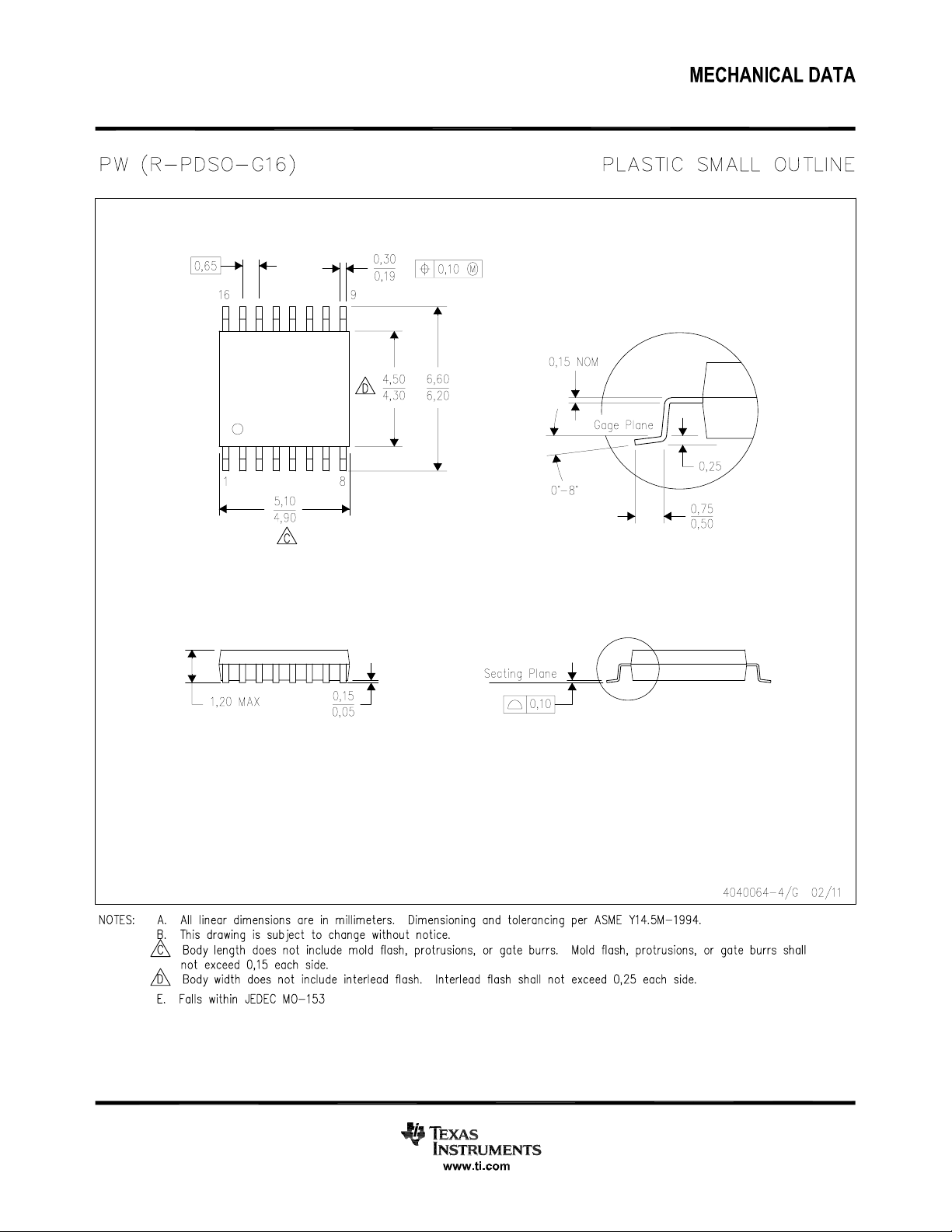
available in a 16-pin TSSOP (PW) package.
absolute maximum ratings over operating free-air temperature (unless otherwise noted)
†w
Input voltage (VIN, VP, VOUT) −0.3 V to 10 V. . . . . . . . . . . . . . . . . . . . . . . . . . . . . . . . . . . . . . . . . . . . . . . .
(BUCK, CCM, CCS, PFM
, SYNC/SD) −0.3 V to VIN + 0.3 V. . . . . . . . . . . . . . . . . . . . . . .
(SWN) −0.3 V to 17 V. . . . . . . . . . . . . . . . . . . . . . . . . . . . . . . . . . . . . . . . . . . . . . . . . . . . . . . .
(SWP) −0.3 V to VIN + 0.3 V. . . . . . . . . . . . . . . . . . . . . . . . . . . . . . . . . . . . . . . . . . . . . . . . . .
Storage temperature range, T
Junction temperature range, T
stg
J
−65°C to 150°C. . . . . . . . . . . . . . . . . . . . . . . . . . . . . . . . . . . . . . . . . . . . . . . . . . . .
−55°C to 150°C. . . . . . . . . . . . . . . . . . . . . . . . . . . . . . . . . . . . . . . . . . . . . . . . . . . .
Lead temperature 1,6 mm (1/16 inch) from case for 10 seconds 300°C. . . . . . . . . . . . . . . . . . . . . . . . . . . . . . . .
†
Stresses beyond those listed under “absolute maximum ratings” may cause permanent damage to the device. These are stress ratings only , a nd
functional operation of the device at these or any other conditions beyond those indicated under “recommended operating conditions” is not
implied. Exposure to absolute- maximum-rated conditions for extended periods may affect device reliability. All voltages are with respect to
ground. Currents are positive into, negative out of the specified terminals.
PW PACKAGE
(TOP VIEW)
SYNC/SD
CCS
RT
CCM
BUCK
PFM
COMP
FB
1
2
3
4
5
6
7
8
16
15
14
13
12
11
10
SWN
SWP
VP
PDRV
GND
NDRV
VOUT
9
VIN
recommended operating conditions
MIN MAX UNIT
Input voltage, VIN, VP 9
Input voltage, VOUT 8
Input voltage, BUCK, CCM, CCS, PFM, SYNC/SD, SWP 9
Input voltage, SWN 17
Operating junction temperature range, TJ
§
t is not recommended that the device operate for extended periods of time under conditions beyond those specified in this table.
2
§
www.ti.com
−40 85 °C
V
Page 3
VP = VOUT = 3.5 V, No load
VP = VOUT = 3.5 V, No load
µA
µA
SLUS489 − OCTOBER 2001
electrical characteristics over recommended operating junction temperature range,
= −40_C to 85_C for the TPS43000, RT = 75 kΩ (500 kHz), VIN = VP = 3.5 V, VOUT = 3.1 V, COMP/FB
T
A
pins shorted, BUCK-configured, T
VIN
PARAMETER TEST CONDITIONS MIN TYP MAX UNIT
Start-up voltage
Undervoltage lockout (UVLO) hysteresis
Shutdown current
Operating current Not in PFM mode, no MOSFETs connected 1.0 1.4 mA
Sleep mode current PFM mode, COMP/FB=900 mV 75 140 µA
BOOST-configured VIN operating current
BOOST-configured VIN sleep mode current
VOUT
PARAMETER TEST CONDITIONS MIN TYP MAX UNIT
Shutdown current SYNC/SD = VIN 0 2
Operating current Not in PFM mode, no MOSFETs connected 1 5
Sleep mode current PFM mode, COMP/FB=900 mV 0 2
BOOST-configured VOUT operating current
BOOST-configured VOUT sleep mode current
= T
(unless otherwise noted)
A
J
1.45 1.65 1.85 V
No MOSFETs connected
SYNC/SD = 1.6 V 1 10
SYNC/SD = VIN 0.5 2
Not in PFM mode, no MOSFETs connected,
BUCK pin grounded, VIN = 3.1 V,
VP = VOUT = 3.5 V
PFM mode, BUCK pin grounded,
VP = VOUT = 3.5 V, VIN = 3.1 V,
COMP/FB=900 mV
Not in PFM mode, no MOSFETs connected,
BUCK pin grounded, VIN = 3.1 V,
VP = VOUT = 3.5 V
PFM mode, BUCK pin grounded,
VP = VOUT = 3.5 V, VIN = 3.1 V,
COMP/FB=900 mV
60 150 300 mV
30 75 µA
25 60 µA
1.0 1.4 mA
50 120 µA
µA
µA
VP
PARAMETER TEST CONDITIONS MIN TYP MAX UNIT
Shutdown current SYNC/SD = VIN 0.5 2
Operating current Not in PFM mode, no MOSFETs connected 500 800
Sleep mode current PFM mode, COMP/FB=900 mV 0 2
error amplifier
PARAMETER TEST CONDITIONS MIN TYP MAX UNIT
VREG, regulation voltage (COMP/FB pin)
FB input current VFB = 800 mV −150 −10 150 nA
Sourcing current (out of COMP) VFB = (VREG − 100 mV), V
Sinking current (into COMP) VFB = (VREG + 100 mV), V
Maximum ouput voltage (COMP pin) VFB = 0 V, I
Minimum output voltage (COMP pin) VFB = 2 V, I
Unity gain bandwidth See Note 1 5 MHz
NOTE 1: Ensured by design. Not production tested.
1.8 V < VIN < 6 V 784 800 816
VIN = 3.5 V 788 800 812
= 0 V, −2.0 −0.5 mA
COMP
= 2 V 0.5 1.2 mA
COMP
= −100 µA 1.6 2.0 V
COMP
= +100 µA 70 120 mV
COMP
µA
mV
www.ti.com
3
Page 4
Soft-start time
Oscillator frequency
Constant current source configured if
Constant current source configured if
SLUS489 − OCTOBER 2001
electrical characteristics over recommended operating junction temperature range,
= −40_C to 85_C for the TPS43000, RT = 75 kΩ (500 kHz), VIN = VP = 3.5 V, VOUT = 3.1 V, COMP/FB
T
A
pins shorted, BUCK-configured, T
soft-start
PARAMETER TEST CONDITIONS MIN TYP MAX UNIT
Soft-start time
oscillator
PARAMETER TEST CONDITIONS MIN TYP MAX UNIT
Oscillator frequency
SYNC/SD
PARAMETER TEST CONDITIONS MIN TYP MAX UNIT
Synchronization threshold voltage 0.8 1.25 1.6 V
SYNC pulse width SYNC/SD = 2 V, COMP/FB=600 mV 100 50 ns
SYNC input current SYNC/SD = 1.6 V 0.5 1 µA
SYNC high to shutdown delay time Float COMP, VFB = 0 V 10 22 35 µs
Synchronous range Force COMP/FB to 600 mV 1.1 f
= T
(unless otherwise noted)
A
J
RT = 37.5 kΩ (1 MHz) 1.0 3.0 6.0
RT = 75 kΩ (500 kHz) 2.0 5.5 12.0
RT = 150 kΩ (250 kHz) 4.0 10.5 24.0
RT = 37.5 kΩ (1 MHz), V
RT = 75 kΩ (500 kHz), V
RT = 150 kΩ (250 kHz), V
= 600 mV 0.90 1.00 1.10 MHz
COMP
= 600 mV 450 500 550 kHz
COMP
= 600 mV 225 250 280 kHz
COMP
o
1.5 f
o
ms
current limit
PARAMETER TEST CONDITIONS MIN TYP MAX UNIT
Hiccup overcurrent threshold voltage Voltage measured from VIN to SWN 175 250 325 mV
Delay to termination of P-channel gate drive time Measured at PDRV 125 300 ns
BOOST configured hiccup overcurrent threshold
voltage
Delay to termination of N-channel gate drive time Measured at NDRV, BUCK grounded 150 300 ns
Consecutive overcurrent clock cycles before
shutdown
Clock cycles before restart 800 900 1000
CCS threshold voltage
CCS pull-down current
CCS current threshold voltage Measured from VIN to SWN 85 150 225
BOOST-configured CCS current threshold voltage
Voltage measured from SWN to GND,
BUCK grounded
V
> 1 V
CCS
Measured from SWN to GND,
BUCK grounded
175 250 325 mV
50 63 75
0.40 0.70 1.00 V
0.5 1.0 µA
85 150 225
mV
4
www.ti.com
Page 5
Continuous conduction allowed if
Continuous conduction allowed if
SLUS489 − OCTOBER 2001
electrical characteristics over recommended operating junction temperature range,
= −40_C to 85_C for the TPS43000, RT = 75 kΩ (500 kHz), VIN = VP = 3.5 V, VOUT = 3.1 V, COMP/FB
T
A
pins shorted, BUCK-configured, T
PWM
PARAMETER TEST CONDITIONS MIN TYP MAX UNIT
BUCK threshold voltage
BUCK pull-down current
BUCK maximum duty cycle VFB = 0 V 100%
BOOST maximum duty cycle BUCK grounded, VFB = 0 V 70% 90%
Minimum duty cycle VFB = 2 V 0%
CCM threshold voltage
CCM pull-down current
BUCK rectifier zero current threshold voltage Measured from SWP to GND −28 −12 0 mV
BOOST rectifier zero current threshold voltage
Delay to termination of P-channel gate drive time Measured at PDRV, BUCK grounded 200 300 ns
= T
(unless otherwise noted)
A
J
BUCK configured if V
V
> 1 V
CCM
Measured from SWP to VOUT,
BUCK grounded
BUCK
> 1 V
0.4 0.7 1.0 V
0.5 1.0 µA
0.4 0.7 1.0 V
0.5 1.0 µA
0 14 32 mV
pulsed frequency modulation
PARAMETER TEST CONDITIONS MIN TYP MAX UNIT
PFM threshold voltage
PFM pull-down current
FB voltage to awaken (exit sleep mode) 768 784 800 mV
Izero pulses required to enter sleep 5 7 9
Start-up delay time after sleep 2 5 µs
PFM mode not allowed if PFM > 1 V
0.4 0.7 1.0 V
0.5 1.0 µA
low power mode
PARAMETER TEST CONDITIONS MIN TYP MAX UNIT
VOUT threshold voltage to enter low power mode VP = VIN = 5 V 3.45 3.60 3.80
VIN threshold voltage to enter low power mode
Hysteresis voltage to exit low power mode
VP = VOUT = 5 V,
BUCK grounded (boost configured)
VOUT < (V
VP = VIN = 5 V
VIN < (V
BUCK grounded, VP = VOUT = 5 V
THRESHOLD−VHYST
THRESHOLD−VHYST
),
),
3.45 3.60 3.80
225 312 415
225 312 415
V
mV
www.ti.com
5
Page 6
C
= 1 nF, VP = VIN = 5 V,
CO = 1 nF, VP = VIN = 5 V,
C
= 1 nF, VIN = 3.1 V,
CO = 1 nF, VIN = 3.1 V,
VP = VIN = 5 V, VOUT = 3.1 V
VP = VIN = 5 V, VOUT = 3.1 V
SLUS489 − OCTOBER 2001
electrical characteristics over recommended operating junction temperature range,
= −40_C to 85_C for the TPS43000, RT = 75 kΩ (500 kHz), VIN = VP = 3.5 V, VOUT = 3.1 V, COMP/FB
T
A
pins shorted, BUCK-configured, T
NDRV
PARAMETER TEST CONDITIONS MIN TYP MAX UNIT
VIN driven rise time
VIN driven fall time
VIN driven pull-up resistance
VIN driven pull-down resistance
BUCK P-channel MOSFET off to N-channel
MOSFET on anti-x delay time
VOUT driven rise time
VOUT driven fall time
VOUT driven pull-up resistance
VOUT driven pull-down resistance
BOOST P-channel MOSFET off to N-channel MOS-
FET on anti-x delay time
= T
(unless otherwise noted)
A
J
VOUT = 3.1 V
VP = VIN = 5 V, VOUT = 3.1 V
VP = VIN = 5 V, VOUT = 3.1 V,
PDRV and NDRV transitioning HI delta
VP = VOUT = 5 V, BUCK grounded
VP = VOUT = VIN = 5 V, LP mode activated
VP = VOUT = 5 V, VIN = 3.1 V,
BUCK grounded
25 45
20 40
6.5 10.0
2.25 4.00
10 35 75
25 45
20 40
6.5 10.0
2.25 4.00
10 35 75 ns
ns
Ω
ns
Ω
PDRV
PARAMETER TEST CONDITIONS MIN TYP MAX UNIT
VP driven rise time
VP driven fall time
VP driven pull-up resistance
VP driven pull-down resistance
BUCK N-channel MOSFET off to P-channel MOS-
FET on anti-x delay time
BOOST N-channel MOSFET off to P-channel MOS-
FET on anti-x delay time
CO = 1 nF
VP = VIN = 5 V, VOUT = 3.1 V
VP = VIN = 5 V, VOUT = 3.1 V,
NDRV and PDRV transitioning LO delta
VP = VOUT = 5 V, VIN = 3.1 V,
BUCK grounded
15 40
15 40
2.5 4.0
3.5 6.0
10 30 75
10 30 75
ns
Ω
ns
6
www.ti.com
Page 7

I/O
DESCRIPTION
SLUS489 − OCTOBER 2001
Terminal Functions
TERMINAL
NAME NO.
Input pin to select topology. Connect this pin to VIN for a buck converter, ground it for a boost or SEPIC.
BUCK 5 I
CCM 4 I
CCS 2 I
COMP 7 O
FB 8 I
GND 12 − Ground pin for the device.
NDRV 11 O
PDRV 13 O
PFM 6 I
RT 3 O A resistor from this pin to ground sets the PWM frequency.
SWP 15 I
SWN 16 I
SYNC/SD 1 I
VP 14 I
VIN 9 I
VOUT 10 O
This configures the logic to the two gate drive outputs, and controls D
pulldown.
Input pin determines whether or not the l
tion. Pulling this pin high ignores the Izero comparator’s output, forcing continuous conduction mode.
Connecting it to ground enables Izero, allowing discontinuous conduction mode (DCM) operation. Note
that even when pulled high, seven detected I
internal pull-down.
Current limit feature allowing selection of either pulse-by-pulse current limiting or hiccup mode overcurrent protection. Connect this pin to VIN to select pulse-by-pulse current limiting, the constant current
source mode. Connect this pin to ground to enable hiccup mode overcurrent protection. This pin has a
weak internal pulldown.
Output of the error amplifier. The compensation components are connected from this pin to the FB pin.
During sleep mode, this pin goes to high impedance, and is severed from the internal error amplifier’s
output so that it may hold its dc potential.
Inverting input to the error amplifier. It is connected to a resistor divider off of VOUT, and to the compensation network.
Gate drive output for the N-channel MOSFET (energizing MOSFET for the boost and SEPIC, rectifier
MOSFET for the buck).
Gate drive output for the P-channel MOSFET (energizing MOSFET for the buck, rectifier MOSFET for the
boost and SEPIC).
Input pin that disables/enables PFM operation. Connecting it to VIN disables PFM mode. Grounding this
pin enables PFM to occur automatically, based on lzero. This pin has a weak internal pulldown.
Connect this pin through a 1-kΩ resistor to the drain of the P-channel MOSFET for all topologies. It detects Izero pulses using the synchronous rectifier MOSFET. For the SEPIC topology, a Schottky clamp
tied to ground must be connected to this pin.
Connect this pin through a 1-kΩ resistor to the drain of the N-channel MOSFET for all topologies. It
senses overcurrent conditions using the inductor energizing MOSFET.
This dual-function pin is used to synchronize the oscillator or shutdown the controller, turning both
MOSFETs off. A pulse from 0 V to 2 V provides synchronization. Duty cycle is not critical, but it must be
at least 100 ns wide. Holding this pin to 2 V or greater for over 35 µs shuts down the device. This pin
has a weak internal pulldown.
Power rail input pin for the P-channel MOSFET gate driver. Connect this pin to VIN for a buck, and to
VOUT for a boost or SEPIC. Provide good local decoupling.
Input supply for the device. It provides power to the device, and may be used for the N−channel gate
drive. Provide good local decoupling
Connect this pin to the power supply output. It may be used for the gate drive to the N−channel MOSFET. Provide good local decoupling.
DESCRIPTION
comparator allows discontinuous conduction mode opera-
ZERO
pulses still initiate PFM mode. This pin has a weak
ZERO
. This pin has a weak internal
MAX
www.ti.com
7
Page 8
3
S
V
V
SLUS489 − OCTOBER 2001
functional block diagram
300 mV
+
10 mV
LEB
+
800 mV
SOFT
START
++
800 mV
784 mV
200 mV
10
VOUT
9
VIN
R
1.6 R
CCM
4
GND
12
SWP
15
6
PFM
784 mV
8
FB
REFGOOD
HICCUP
7COMP
RT
3
YNC/SD
1
5
BUCK
2
CCS
150 mV
++
250 mV
SWN LEB
16
VREF
1.246 V
SHUTDOWN
TIMER AND
OSCILLATOR
SHUTDOWN
(SD)
+
UVLO
95% MAXIMUM DUTY
CYCLE NON−BUCK
+
+
DELAY
TO ZERO
IZERO
ERROR
AMPLIFIER
+
+
SLEEP
RESET
VINEST 2.75 V
VBEST
REFGOOD
REFBAD
RECTOFF
(STOP SWITCH
RECTIFICATION)
3−BIT UP
COUNTER
PWM
COMPARATOR
+
RESET
6−BIT
UP/DOWN
COUNTER
IMAX
(STOP ENERGIZING INDICATOR)
SQ
SQ
QR
VIN
VOUT
SLEEP
QR
RECTOFF IMAX
RECTIFY
RESET
SHUTDOWN
FOR 900
CYCLES THEN
SOFT−START
+
VINEST
LPM
VINEST
CONDUCTION
TOPOLOGY
PWM ENABLE
HICCUP
(STOP SWITCHING FOR 900
CYCLES THEN SOFT−START)
VDD
3.6 V
3.3 V
ANTI
CROSS
&
STEERING
LOGIC
+
+
SQ
QR
VIN
NDRV_RAIL
SD
REFBAD
SLEEP
HICCUP
LPM
VOUT
VP
14
PDR
13
NDR
11
TPS43000
8
www.ti.com
UDG−0104
Page 9

SLUS489 − OCTOBER 2001
APPLICATION INFORMATION
general information
The TPS43000 is a high-frequency, synchronous PWM controller optimized for distributed power, or
battery-powered applications where size and efficiency are of critical importance. It includes high-speed,
high-current MOSFET drivers for those applications requiring low R
block diagram).
optimizing efficiency
The TPS43000 optimizes efficiency and extends battery life with its low quiescent current and its synchronous
rectifier topology . The additional features of low-power (LP) mode and PFM mode maintain high efficiency over
a wide range of load current.
modes of operation
The TPS43000 has four distinct modes of operation:
D fixed PWM with discontinuous conduction mode (DCM) possible
external MOSFETs. (See functional
DS(on)
D fixed PWM with forced continuous conduction mode (CCM)
D automatic pulse frequency modulation (PFM) with DCM possible
D PFM with forced CCM
The device mode is controlled by the CCM and PFM
DCM by connecting the pin to ground or to force CCM by connecting the pin to VIN. The PFM
decide whether to allow automatic PFM by connecting the pin to ground or to force fixed PWM by connecting
the pin to VIN.
fixed PWM with DCM possible (PFM tied to VIN; CCM tied to ground)
In this mode, the device behaves like a standard switching regulator with the addition of a synchronous rectifier.
Shortly after the energizing MOSFET turns off, the synchronous rectifier turns on. The synchronous rectifier
turns off either when the inductor current goes discontinuous (DCM) or just prior to the start of the next clock
cycle (CCM) when the energizing MOSFET turns on. During the small time interval when neither the energizing
MOSFET nor the synchronous rectifier are turned on, the synchronous rectifier MOSFET body diode (or an
optional small external Schottky diode in parallel) carries the current to the output until it goes discontinuous.
The efficiency drops off at light loads as the losses become a larger percentage of the delivered load.
pins. The CCM pin lets the user decide whether to allow
pin lets the user
www.ti.com
9
Page 10

(1)
SLUS489 − OCTOBER 2001
APPLICATION INFORMATION
fixed PWM with forced CCM (PFM and CCM tied to VIN)
CCM is forced under all operating conditions in this mode. The synchronous rectifier turns on shortly after the
energizing MOSFET turns off and remains on until just prior to the start of the next clock cycle when the
energizing MOSFET turns on. The user should design the converter to operate in CCM over its entire operating
range in order to prevent the inductor current from going negative. If the converter is allowed to run
discontinuous, the inductor current goes negative (i.e. the output discharges as the current reverses and goes
back through the rectifier to the input or ground.) With fixed PWM, the efficiency drops off at light loads as the
losses become a larger percentage of the delivered load.
PFM with DCM possible (PFM
In this mode, the device can operate in either fixed PWM or in PFM mode. When the device is initially powered,
it operates in fixed PWM mode until soft-start completion. It remains in this mode until it senses that the converter
is on the verge of breaking into discontinuous operation. When this condition is sensed, the converter enters
PFM mode, invoking a sleep state until the output voltage falls 2% below nominal (a 16-mV drop measured at
the FB pin). At this time, the controller starts up again and operates at its fixed PWM frequency for a short
duration (load dependent, typically 10 to 200 PWM cycles), increasing the output voltage. If the controller again
senses the converter is on the verge of going discontinuous, the cycle repeats. If discontinuous operation is not
sensed, the converter remains in fixed PWM mode. PFM mode results in a very low duty cycle of operation,
reducing all losses and greatly improving light load efficiency. During the sleep state, most of the circuitry internal
to the TPS43000 is powered down. This reduces quiescent current, which lowers the average dc operating
current, enhancing its efficiency.
PFM with forced CCM (PFM
This mode is similar to the PFM with DCM possible mode except that the controller forces the converter to
operate in CCM. The converter can be designed to run discontinuous at light loads. The controller senses
discontinuous operation and enters the PFM mode. With PFM, the converter can maintain a very high efficiency
over a very wide range of load current.
and CCM tied to ground)
tied to ground; CCM tied to VIN)
anticross−conduction and adaptive synchronous rectifier commutation logic
When operating in the continuous conduction mode (CCM), the energizing MOSFET and the synchronous
rectifier MOSFET are simply driven out of phase, so that when one is on the other is off. There is a built-in time
delay of about 40 ns to prevent any cross-conduction.
In the event that the converter is operating in the discontinuous conduction mode (DCM), the synchronous
rectifier needs to be turned off quickly, when the rectifier current drops to zero. Otherwise, the output begins to
discharge as the current reverses and goes back through the rectifier to the input or ground (this obviously
cannot happen when using a conventional diode rectifier). To prevent this, the TPS43000 incorporates a
high-speed comparator that senses the voltage on the synchronous rectifier using the SWP input, which is
connected to the synchronous rectifier MOSFET’s drain through a 1-kΩ resistor. This comparator is used to
determine when the inductor current is on the verge of going discontinuous and is referred to as the I
comparator. I n the boost and SEPIC (single-ended primary inductance converter) topologies, the synchronous
rectifier is turned off when the voltage on the SWP pin decreases to within 12 mV of VOUT. For this reason, it
is important to have the VOUT pin well decoupled. In the buck topology, the synchronous rectifier is turned off
when the voltage on the SWP pin increases to −12 mV with respect to ground. The I
as follows:
+
12 mV
R
DS(on)
www.ti.com
10
l
ZERO
threshold is defined
ZERO
ZERO
Page 11

(2)
SLUS489 − OCTOBER 2001
APPLICATION INFORMATION
When the R
comparator is enabled, the MOSFET must be fully enhanced, and the drain-to-source voltage must be allowed
to settle. The TPS43000 has an internal circuit that enables the I
the rectifier MOSFET is enhanced.
NOTE: For the SEPIC topology, the voltage on the drain of the rectifier MOSFET swings to −VIN
when the energizing MOSFET is on. Therefore, in order to prevent the SWP input pin from being
damaged, it must connect to a Schottky diode clamp to ground.
PFM mode
For improved efficiency at light loads, the TPS43000 can be programmed to automatically enter PFM (Pulse
Frequency Modulation) mode by connecting the PFM
used for synchronous rectifier commutation. An internal digital counter is used to count the number of I
pulses at the output of the I
until the voltage at the FB pin falls to approximately 784 mV (output voltage drops 2% below nominal). At this
time, the controller turns back on and operates at its fixed-frequency for a short duration (load dependent,
typically 10 to 200 PWM cycles) increasing the output voltage. The cycle repeats when another seven I
pulses occur. This results in a very low duty cycle of operation, reducing all losses and improving light load
efficiency. During the sleep state, most of the circuitry internal to the TPS43000 is powered down. This reduces
quiescent current, which lowers the average dc operating current, enhancing its efficiency. The error amplifier
output is disconnected from the COMP pin during the sleep state. The COMP pin goes to high impedance and
maintains approximately the same voltage level it was at when it entered the sleep state. This minimizes error
amplifier overshoot/undershoot when coming out of the sleep state. The user can disable PFM by connecting
the PFM
low power mode
pin to VIN.
of the MOSFET is used as the sense element, several issues arise. Before the I
DS(on)
comparator approximately 40 ns after
ZERO
pin to ground. PFM is initiated by the I
comparator. When seven I
ZERO
pulses occur, the controller enters sleep state
ZERO
ZERO
ZERO
comparator
ZERO
ZERO
At relatively high gate drive voltages, gate drive losses can become excessive and begin to dominate under light
load conditions. The expression for gate drive power loss is given by equation (2). The power varies as a function
of the applied gate voltage squared.
2
ǒ
Ǔ
f
Q
P
GATELOSS
where Q
V
is the applied gate drive voltage, and f is the switching frequency.
G
When both VIN and VOUT are above 3.6 V, the TPS43000 automatically enters LP mode and selects the lower
voltage of VIN or VOUT to provide the gate drive voltage on the NDRV pin. This minimizes gate drive losses
at relatively high input and output voltages and helps maintain high efficiency at light loads. The PDRV pin
remains powered by either VIN (buck topology) or VOUT (boost, flyback, and SEPIC topologies) via the VP
power input pin.
To help provide a smooth transition in and out of LP mode, its circuitry has 300 mV of hysteresis. When either
VIN or VOUT drops below 3.3 V, the TPS43000 transitions back to normal mode and the NDR V pin is powered
by the higher potential of VIN or VOUT.
is the total gate charge, VS is the gate voltage specified in the MOSFET manufacturer’s data sheet,
G
+
V
G
G
V
S
,
www.ti.com
11
Page 12

(3)
(4)
SLUS489 − OCTOBER 2001
APPLICATION INFORMATION
synchronization and shutdown
The TPS43000 incorporates a dual function synchronization and shutdown pin. It may be used to synchronize
the TPS43000’s switching frequency to an external clock, or to shutdown the device entirely.
To synchronize the internal clock to an external source, the SYNC/SD pin must be driven high, greater than
1.6 V. The circuitry synchronizes to the rising edge of the input. Duty cycle is not critical, but the pulse width must
be at least 100 ns wide but less than 10 µs to avoid shutdown. The external SYNC clock should be between
10% and 25% above the free-running switching frequency.
To ensure a shutdown of the converter, the SYNC/SD pin must be held high (above 1.6 V) for a minimum of
35 µs. In shutdown, both the energizing and rectifier MOSFETs are turned off. The quiescent current is reduced
to less than 10 µA with 1.6 V applied to SYNC/SD and less than 2 µA with VIN potential applied to SYNC/SD.
Bringing this pin low again allows the device to resume operation, starting with a full soft-start cycle.
overcurrent protection
The TPS43000 allows the user to select either pulse-by-pulse current limiting or hiccup mode overcurrent
protection using the CCS pin. To minimize external part count and minimize losses, the energizing MOSFET’s
R
to as the I
is connected to the energizing MOSFET’s drain through a 1-kΩ resistor. The I
SWN input to either ground (boost, flyback, and SEPIC topologies) or VIN (buck topology). Before the I
comparator is enabled, the energizing MOSFET must be fully enhanced, and the drain-to-source voltage must
be allowed to settle. The TPS43000 has an internal circuit that enables the I
60 ns after the energizing MOSFET is enhanced.
is used as the current sense element. The TPS43000 incorporates a high-speed comparator, referred
DS(on)
comparator, that senses the voltage across the energizing MOSFET using the SWN input ,which
MAX
comparator compares its
MAX
comparator approximately
MAX
MAX
pulse-by-pulse current limiting − constant current source mode (CCS tied to VIN)
In the pulse-by-pulse current limiting mode, the energizing MOSFET gate drive is terminated once the
overcurrent threshold is reached. An overcurrent, I
, is sensed when the voltage drop across the energizing
MAX
MOSFET reaches 150 mV. The pulse-by-pulse current limiting threshold is defined by the equation:
I
MAX(pp)
+
R
150 mV
DS(on)
In the boost, flyback, and SEPIC topologies, IMAX(pp) is reached when the voltage on the SWN pin is 150 mV
above ground. In the buck topology, IMAX(pp) is reached when the voltage on the SWN pin is 150 mV below
VIN. For this reason, it is important to have the VIN pin well decoupled. Pulse-by-pulse current limiting is enabled
by connecting the CCS input pin to VIN.
hiccup mode over current protection (CCS tied to ground)
In the hiccup mode overcurrent protection scheme, an internal digital counter is used to count the number of
I
pulses at the output of the I
MAX
comparator. An I
MAX
condition is sensed when the voltage drop across
MAX
the energizing MOSFET reaches 250 mV. The hiccup mode overcurrent threshold is defined by the equation:
I
MAX(hu)
In the boost, flyback, and SEPIC topologies, I
250 mV above ground. In the buck topology, I
is 250 mV below VIN. When 63 I
+
R
250 mV
DS(on)
MAX(hu)
MAX(hu)
MAX(hu)
condition is reached when the voltage on the SWN pin is
condition is reached when the voltage on the SWN pin
pulses are reached, both the energizing MOSFET and rectifier MOSFET
are turned off. The MOSFET switches are held off for 882 clock cycles before a soft-start is initiated. Hiccup
mode overcurrent protection is enabled by connecting the CCS input pin to ground.
12
www.ti.com
Page 13
(5)
SLUS489 − OCTOBER 2001
APPLICATION INFORMATION
start-up and soft-start
The TPS43000 incorporates an UVLO circuit that disables the output drivers when the voltage at the VIN pin
is below 1.65 V. In order to prevent the converter from oscillating during low input voltage startup, the UVLO
circuit is designed with 200 mV of hysteresis and the converter remains on until VIN drops below 1.45 V.
The TPS43000 has a built-in soft-start that varies as a function of the switching frequency. The soft-start is a
closed-loop soft-start, meaning that the reference input to the error amplifier is ramped up over the soft-start
interval and the converter control loop is allowed to track the ramping reference signal. The soft-start interval
is set to approximately 2000 oscillator clock cycles. This method generally allows for faster soft-start times with
minimal output voltage overshoot at startup. During start-up, the synchronous rectifier is held off until the COMP
pin reaches 700 mV.
programming the PWM frequency
The oscillator frequency is programmed by a resistor from the RT pin to ground. The approximate operating
frequency is determined by the equation:
fSW(MHz) +
38
(kW)
R
T
The maximum operating frequency is 2 MHz. Some applications may want to remain in a fixed-frequency mode
of operation, even at light load, rather than going into PFM mode. This lowers efficiency at light load. One way
to improve the efficiency while maintaining fixed frequency operation is to lower the PWM frequency under
light-load conditions. This can be easily done, as shown in Figure 1. By adding a second timing resistor and a
small MOSFET switch, the host can switch between two discrete frequencies at any time.
TPS43000
SWN
SWP
VP
PDRV
GND
NDRV
VOUT
VIN
16
15
14
13
12
11
10
9
FREQUENCY
CONTROL
2N7002
V
OUT
RT2
R1
RT1
SYNC/SD
1
2
CCS
3
RT
4
CCM
5
BUCK
6
PFM
7
COMP
8
FB
R2
Figure 1. Changing the PWM Frequency
www.ti.com
UDG−01035
13
Page 14

C2
SLUS489 − OCTOBER 2001
APPLICATION INFORMATION
error amplifier
The TPS43000 uses voltage mode control for each of the topologies. The output voltage is sensed and fed back
to the FB pin (inverting input) and compared to an internal 800 mV reference connected to the non-inverting
input. The difference (i.e. error voltage), is amplified by the internal error amplifier. The output of the error
amplifier (COMP), is then compared to the oscillator sawtooth ramp to control the pulse width used to drive the
power switch (energizing MOSFET). The duty cycle is varied to regulate the output voltage. The higher the error
voltage, the longer the energizing MOSFET switch is on.
The transient response of a converter is a function of both small signal and large signal responses. The small
signal response is determined by the error amplifier’s loop compensation (feedback network), whereas the large
signal response is a function of the error amplifier’s gain bandwidth and slew rate (dv/dt) as well as the slew
rate of the inductor current (di/dt). The TPS43000 internal error amplifier has a 5-MHz unity gain bandwidth. This
almost assures that the loop bandwidth is limited by external circuit characteristics rather than error amplifier
limitations. The internal error amplifier is capable of sourcing and sinking an ensured 500 µA, which assures
that even during large signal transients, external components determine circuit behavior. Using low feedback
capacitance allows the error amplifier to rapidly slew from one level to another, insuring excellent transient
response.
loop compensation
The voltage loop needs to be compensated to provide control loop stability margin, and to minimize the output
voltage overshoot/undershoot response to line and load transients. A Type III error amplifier compensation
network can be used to optimize the loop response for any of the topologies and operating modes implemented
with the TPS43000. The T ype III amplifier circuit is shown in Figure 2. This configuration has a pole at the origin
and two zero-pole pairs. It can provide up to 180° of phase boost.
Av1
R3
VOUT
C3
R1
Figure 2. Type III Error Amplifier Compensation
Network
R
BIAS
R2
V
REF
C1
+
0 dB
Gain − dB
Av2
fz1 fz2 fp1 fp2
t − Time − ns
Figure 3. Type III Error Amplifier Compensation
Gain Response
14
www.ti.com
Page 15

(6)
(7)
(8)
(9)
(10)
(11)
(12)
(13)
(14)
APPLICATION INFORMATION
The frequency of the poles and zeros are defined by the following equations:
zeros
f
+
z1
(
2p R2 C1
1
)
SLUS489 − OCTOBER 2001
f
[
z2
(
2p R1 C3
poles
f
+
p1
(
f
[
p2
(
In voltage mode control, the buck, boost, flyback, and SEPIC toplogies all have a 2
characteristic when operated in CCM. In the buck topology, the frequency of the LC double pole is straight
forward.
f
+
LC
ǒ
In the boost, flyback, and SEPIC toplogies, the frequency of the LC double pole varies as a function of the duty
cycle.
f
+
LC
ǒ
In addition, each of the topologies have an ESR zero, which occurs when the output capacitor impedance
transitions from capacitive to resistive. The frequency at which this occurs is the ESR zero frequency, f
is defined by the equation:
1
1
2p R3 C3
1
2p R2 C2
1
1ń2
Ǔ
)
2p(LC
(
2p(LC
1 * D
)
)
1ń2
Ǔ
, assuming R1 ơ R3
)
)
, assuming C1 ơ C2
)
buck topology
boost, flyback, & SEPIC topologies
nd
order double-pole LC filter
ESR
, and
f
+
ESR
In the boost, flyback, and SEPIC topologies operated in CCM, there is also a right half-plane (RHP) zero. The
RHP zero has the same positive gain slope as the conventional zero, but has a 90° phase lag. This combination,
in conjunction with its dependence on line and load, make it nearly impossible to compensate within the control
loop. The frequency at which this RHP zero occurs, f
f
RHP
f
RHP
where RO is the equivalent output load resistance.
2p
R
+
R
+
ǒ
O
O
1
R
ESR
(
1 * D
(
2 p L
(
1 * D
(
2 p LD
Ǔ
)
)
C
2
)
boost topology
2
)
flyback topology
RHP
www.ti.com
, is defined by the equations:
15
Page 16

(15)
(16)
SLUS489 − OCTOBER 2001
APPLICATION INFORMATION
With voltage-mode control, the closed-loop design goal for each of the topologies with the T ype III error amplifier
compensation is to set the crossover frequency above the resonant frequency of the LC filter (prevents filter
oscillations during a transient response), but below the lowest possible RHP zero frequency. This is
accomplished by setting the two zeros in the compensation network before the LC double pole frequency. This
provides a phase boost. The two poles should be placed a decade above the crossover frequency.
The following is a typical procedure for selecting the loop compensation values for a buck converter operated
in CCM:
Step 1. Select the desired crossover frequency a decade above the LC pole frequency.
Step 2. Set the resistor divider formed by R1 and R
R
sets the dc operating point of the loop, but has no effect on ac operation and does not factor into
BIAS
the loop compensation calculations.
Step 3. Set the zero formed by R1 and C3 to approximately one-half decade above the LC double pole to
compensate for the phase loss.
Step 4. Set the zero formed by R2 and C1 to approximately one-half decade below the LC double pole to avoid
a conditional instability.
Step 5. Set the pole formed by R3 and C3 to cancel the ESR zero of the output capacitor.
Step 6. Set the pole formed by R2 and C2 to approximately one-half decade above the crossover frequency.
to develop the desired regulation voltage. Note that
BIAS
If the converter is operated in DCM, the lead network (R3 and C3 in Figure 2) can be eliminated for all topologies.
This configuration is referred to as a Type II error amplifier compensation network and has a pole at the origin
and a single zero-pole pair. It can provide up to 90° of phase boost. The frequency of the pole and zero are
defined by the following equations:
zero
f
+
z1
(
2p R2 C1
pole
f
[
p1
(
2p R2 C2
The zero-pole pair is used to compensate for the power circuit’s ESR zero and the pole formed by the output
capacitor and the effective output resistance.
1
)
1
, Assuming C1 ơ C2
)
16
www.ti.com
Page 17

(17)
SLUS489 − OCTOBER 2001
APPLICATION INFORMATION
design examples: buck, boost, non-synchronous boost, flyback, and SEPIC
buck converter
The buck topology is simple and efficient, and should be used whenever the desired output voltage is less than
the minimum input voltage. Figure 4 shows the TPS43000 in a typical (750 kHz) buck converter with an input
voltage range of 3.0 V to 9.0 V, an output voltage of 2.7 V, and a load current from 0 A to 2 A.
Q2
16
15
14
13
12
11
10
9
Si9803DY
R5
1 kΩ
C5
0.47µF
C6
0.47µF
V
IN
0.47µF
V
IN
C2
10 pF
100µF
R4
49.9 kΩ
C1
560 pF
R2
75 kΩ
C7
1
SYNC/SD
2
CCS
RT
3
CCM
4
5
BUCK
6
PFM
7
COMP
8
FB
TPS43000
C3
100 pF
SWN
SWP
VP
PDRV
GND
NDRV
VOUT
VIN
R3
49.9 kΩ
3.3µH
Q1
Si9804DY
C4
L1
D1
ZHCS1000
(OPTIONAL)
C8
120 µF
V
OUT
V
IN
R1
127 kΩ
R
BIAS
53.6 kΩ
Figure 4. 2.7-V Output Buck Topology
For a buck converter, the average output current is related to the peak inductor current by:
Ipk+ I
OUT
ǒ
)
VIN* V
ǒ
2 fSW L
OUT
Ǔ
D
Ǔ
www.ti.com
UDG−01035
17
Page 18

(18)
SLUS489 − OCTOBER 2001
APPLICATION INFORMATION
where fSW is the switching frequency , L is the inductor value, and D is the duty cycle. The duty cycle for a buck
converter is defined as:
V
OUT
D +
V
IN
Note that in these equations the voltage drop across the rectifier has been neglected.
boost converter
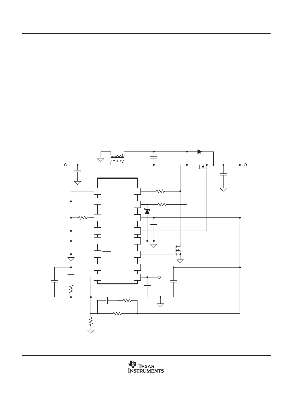
The boost topology is simple and efficient, and should be used whenever the desired output voltage is greater
than the maximum input voltage. Figure 5 shows the TPS43000 in a typical (750 kHz) boost converter with an
input voltage range of 2.5 V to 4.5 V, an output voltage of 5.0 V, and a load current from 0 A to 1 A.
D1
L1
3.3 µH
V
IN
C7
100 µF
R5
1 kΩ
1
SYNC/SD
TPS43000
SWN
16
ZHCS1000
(OPTIONAL)
Q2
Si9803DY
C8
120 µF
V
OUT
C2
330 pF
R4
49.9 kΩ
C1
3300 pF
R2
30.1 kΩ
2
CCS
3
RT
4
CCM
5
BUCK
6
PFM
7
COMP
8
FB
R
BIAS
53.6 kΩ
C3
680 pF
280 kΩ
R1
SWP
VP
PDRV
GND
NDRV
VOUT
VIN
24.9 kΩ
R3
15
14
13
12
11
10
C6
0.47 µF
Q2
Si9804DY
9
C5
0.47 µF
V
IN
C4
0.47 µF
UDG−01037
18
Figure 5. 5-V Output Boost Topology
www.ti.com
Page 19

(19)
(20)
SLUS489 − OCTOBER 2001
APPLICATION INFORMATION
For a boost converter, the average output current is related to the peak inductor current by the following
equation:
ǒ
V
I
+
ǒ
V
OUT
ǒ
OUT
V
h V
* V
OUT
I
pk
where fSW is the switching frequency , L is the inductor value, and D is the duty cycle. The duty cycle for a boost
converter is defined as:
D +
Note that in these equations the voltage drop across the rectifier has been neglected.
non−synchronous boost converter
The TPS43000 can also be used in non-synchronous applications to provide output voltages greater than 8 V
from low voltage inputs. Figure 6 shows the TPS43000 in a non-synchronous boost converter (750 kHz)
application with an input voltage range of 2.5 V to 9.0 V, an output voltage of 12 V, and a load current from 0
A to 1 A. Since none of the device pins are exposed to the boosted voltage, the output voltage is limited only
by the ratings of the external MOSFET, rectifier, and filter capacitor. At these higher output voltages, good
efficiency is maintained since the rectifier drop is small compared to the output voltage. Note that the PFM mode
can still be used to maintain high efficiency at light load.
Since all the power supply pins (VIN, VOUT, VP) operate off the input voltage, it must be greater than 2.5 V and
high enough to assure proper gate drive to the charge MOSFET.
OUT
IN
IN
Ǔ
ǒ
VIN D
)
Ǔ
ǒ
2 fSW L
Ǔ
Ǔ
Ǔ
www.ti.com
19
Page 20

SLUS489 − OCTOBER 2001
APPLICATION INFORMATION
V
IN
C2
330 pF
100 µF
R4
49.9 kΩ
C1
3300 pF
R2
30.1 kΩ
C7
1
SYNC/SD
2
CCS
3
RT
4
CCM
5
BUCK
6
PFM
7
COMP
8
FB
3.3 µH
TPS43000
C3
680 pF
L1
SWN
SWP
VP
PDRV
GND
NDRV
VOUT
VIN
R3
24.9 kΩ
16
15
14
13
12
11
10
D1
ZHCS1000
V
OUT
C8
120 µF
R5
1 kΩ
V
IN
C6
0.47 µF
Q2
Si9804DY
V
IN
9
C5
0.47 µF
V
IN
C4
0.47 µF
R1
750 kΩ
R
BIAS
53.6 kΩ
Figure 6. 12-V Output Non-Synchronous Boost Topology
UDG−01038
20
www.ti.com
Page 21

SLUS489 − OCTOBER 2001
APPLICATION INFORMATION
flyback converter
A flyback converter (750 kHz) using the TPS43000 is shown in Figure 7. It uses a standard two-winding coupled
inductor with a 1:1 turns ratio. The advantage of this topology is that the output voltage can be greater or less
than the input voltage. For example, this is ideal for generating 3.3 V from a lithium-ion cell.
L1B
V
IN
C7
100 µF
1
2
R4
49.9 kΩ
3
4
L1A
3.3 µH
TPS43000
SYNC/SD
CCS
RT
CCM
SWN
SWP
VP
PDRV
R5 1 kΩ
16
R6 1 kΩ
15
14
C6
0.47 µF
13
D1
ZHCS1000
(OPTIONAL)
Q2
Si9803DY
C8
120 µF
V
OUT
R1
169 kΩ
GND
NDRV
VOUT
VIN
R3
6.81 kΩ
12
11
10
Q1
Si9804DY
C5
0.47 µF
V
IN
C4
0.47 µF
9
C2
82 pF
C1
3900 pF
R2
24.9 kΩ
5
BUCK
6
PFM
7
COMP
8
FB
1200 pF
R
BIAS
53.6 kΩ
C3
Figure 7. 3.3-V Output Flyback Topology
NOTE: Resistor-capacitor snubbers can be placed across the primary and secondary windings to
reduce ringing due to leakage inductance. These are optional, and may not be required in the
application.
UDG−01039
For a flyback converter, the average output current is related to the peak inductor current by:
www.ti.com
21
Page 22
(21)
(22)
SLUS489 − OCTOBER 2001
ǒ
V
I
+
pk
OUT
ǒ
h V
I
OUT
IN
Ǔ
ǒ
VIN D
Ǔ
)
Ǔ
ǒ
2 fSW L
Ǔ
where fSW is the switching frequency , L is the inductor value, and D is the duty cycle. The duty cycle for a flyback
converter is defined as:
V
ǒ
VIN) V
OUT
OUT
Ǔ
D +
Note that in these equations the voltage drop across the rectifier has been neglected.
SEPIC converter
The TPS43000 may also be used in the SEPIC topology. This topology, which is similar to the flyback, uses a
capacitor to aid in energy transfer from input to output. Figure 8 shows the TPS43000 in a SEPIC converter
(750 kHz) application with an input voltage range of 2.5 V to 6.0 V, an output voltage of 3.3 V, and a load current
from 0 A to 1 A.
L1B
C9
V
IN
C7
100 µF
1
2
R4
49.9 kΩ
3
4
L1A
4.9 µH
TPS43000
SYNC/SD
CCS
RT
CCM
SWN
SWP
VP
PDRV
16
15
14
13
10 µF
R5 1 kΩ
R6 1 kΩ
D1 BAT54
C6
0.47 µF
D1
ZHCS1000
(OPTIONAL)
Q2
Si9803DY
C8
120 µF
V
OUT
22
C2
82 pF
C1
3900 pF
R2
24.9 kΩ
R1
169 kΩ
GND
NDRV
VOUT
VIN
R3
6.81 kΩ
12
11
10
9
C5
0.47 µF
0.47 µF
5
BUCK
PFM
6
COMP
7
8
FB
C3
1200 pF
R
BIAS
53.6 kΩ
Figure 8. 3.3-V Output SEPIC Topology
www.ti.com
Q1
Si9804DY
C4
UDG−01040
Page 23

(23)
(24)
SLUS489 − OCTOBER 2001
APPLICATION INFORMATION
The SEPIC topology offers the same advantage of the flyback in that it can generate an output voltage that is
greater or less than the input voltage. However, it also offers improved efficiency. Although it requires an
additional capacitor in the power stage, it greatly reduces ripple current in the input capacitor and improves
efficiency by transferring the energy in the leakage inductance of the coupled inductor to the output. This also
provides snubbing for the primary and secondary windings, eliminating the need for RC snubbers. Note that
the capacitor must have low ESR, with sufficient ripple current rating for the application. Another advantage of
the SEPIC is that the inductors do not have to be on the same core.
theory of operation
When the energizing MOSFET (Q1) is on, V
At the same time, the voltage across the SEPIC capacitor C9 (equal to V
end also negative. Since L1A = L1B and the voltages across the two inductors are equal (V
currents ramp up at the same rate (di/dt=V
currents. When the energizing MOSFET turns off, the inductor current wants to continue to flow causing the
inductor voltages to reverse until the output rectifer begins to conduct. The voltage across L1B is clamped to
V
(plus the rectifier drop) and with its dotted end positive. The voltage across the SEPIC capacitor (VIN)
OUT
cancels with V
and the voltage across the two inductors are equal (V
(di/dt=V
by L1B when the energizing MOSFET is on. Since the voltages across the inductors are identical at all times
throughout the switcing cycle, the inductors can be coupled on a single magnetic core with an equal number
of turns. This improves the SEPIC application’s dynamic performance and also allows reduction of the input
filtering requirements through ripple steering.
OUT
and the voltage across L1A is also V
IN
/L). The SEPIC capacitor is charged by L1A when the energizing MOSFET is off and is discharged
is applied across L1A with the dotted end negative (see Figure 8).
IN
/L). The energizing MOSFET current is the sum of the two inductor
IN
with its dotted end positive. Again, since L1A=L1B
OUT
), the inductor current ramps down at the same rate
OUT
) is applied across L1B with its dotted
IN
), the inductor
IN
selecting the inductor
The inductor must be chosen based on the desired operating frequency and the maximum load current. Higher
frequencies allow the use of lower inductor values, reducing component size. Higher load currents require larger
inductors with higher current ratings and less winding resistance to minimize losses. The inductor must be rated
for operation at the highest anticipated peak current. Refer to equations 17, 19, and 21 to calculate the peak
inductor current for a buck, boost, flyback, or SEPIC design, based on VIN, VOUT, duty cycle, maximum load,
frequency, and inductor value. Some manufacturers rate their parts for maximum energy storage in microjoules
(µJ). This is expressed by:
2
ǒ
E + 0.5 L
where E is the required energy rating in microjoules, L is the inductor value in microhenries (µH) (with current
applied), and Ipk is the peak current in amps that the inductor sees in the application. Another way in which
inductor ratings are sometimes specified is the maximum volt-seconds applied. This is given simply by:
ǒ
VIN D
ET +
where ET is the required rating in V-µs, D is the duty cycle for a given VIN and V
frequency in MHz. Refer to equations 18, 20, and 22 to calculate the duty cycle for a buck, boost, flyback, or
SEPIC converter.
In any case, the inductor must use a low loss core designed for high-frequency operation. High-frequency ferrite
cores are recommended. Some manufacturers of off-the-shelf surface-mount designs are listed in Table 1. For
flyback and SEPIC topologies, use a two-winding coupled inductor. SEPIC designs can also use two discrete
inductors.
f
SW
Ǔ
I
pk
Ǔ
, and fSW is the switching
OUT
www.ti.com
23
Page 24

SLUS489 − OCTOBER 2001
APPLICATION INFORMATION
Table 1. SMT Commercial Inductor Manufacturers
Coilcraft Inc. (800) 322−2645 1102 Silver Lake RD, Cary, IL 60013
Coiltronics Inc. (407) 241−7876 6000 Park of Commerce Blvd, Boca Raton, FL 33487
Dale Electronics, Inc. (605) 665−9301 East Highway 50, Yankton, SD 57078
Pulse Engineering Ltd. (204) 633−432 1300 Keewatin Street, Winnipeg, MB R2X 2R9
Sumida
BH Electronics (612) 894−9590 12219 Wood Lake Drive, Burnsville, MN 55337
Tokin America Inc. (408) 432−8020 155 Nicholson Lane, San Jose CA 95134
1−847−545−6700
Fax 1−847−545−6720
selecting the filter capacitor
The input and output filter capacitors must have low ESR and low ESL. Surface-mount tantalum, OSCONs or
multilayer ceramics (MLCs) are recommended. The capacitor selected must have the proper ripple current
rating for the application. Some recommended capacitor types are listed in Table 2.
1701 Golf Road, Tower 3, Suite 400,
Rolling Meadows, IL 60008
Table 2. Recommended SMT Filter Capacitors
Manufacturer Part Number Features
AVX TPS series Low ESR tantalum
Kemet T410 series Low ESR tantalum
Murata GRM series Low ESR ceramic
Sanyo OSCON series Low ESR organic
Sprague
Tokin Y5U, Y5V Type Low ESR ceramic
Taiyo Yuden X5R Type Low ESR ceramic
591D series Low ESR, low profile tantalum
594D series Low ESR tantalum
circuit layout and grounding
As with any high-frequency switching power supply, circuit layout, hookup, and grounding are critical for proper
operation. Although this may be a relatively low-power , low-voltage design, these issues are still very important.
The MOSFET turn-on and turn-off times necessary to maintain high efficiency at high switching frequencies of
1 MHz or more result in high dv/dt and di/dts. This makes stray circuit inductance especially critical. In addition,
the high impedances associated with low-power designs, such as in the feedback divider, make them especially
susceptible to noise pickup.
layout
The component layout should be as tight as possible to minimize stray inductance. This is especially true of the
high-current paths, such as in series with the MOSFETs and the input and output filter capacitors.
The components associated with the feedback, compensation and timing should be kept away from the power
components (MOSFETs, inductor). Keep all components as close to the device pins as possible. Nodes that
are especially noise sensitive are the FB, RT and COMP pins.
24
www.ti.com
Page 25

(25)
SLUS489 − OCTOBER 2001
APPLICATION INFORMATION
grounding
A ground plane is highly recommended. The GND pin of the TPS43000 should be close to the source of the
N-channel MOSFET, the input filter capacitor, and the output filter capacitor. The grounded end of the RT
resistor, the feedback divider resistor, and the SYNC/SD, CCS, CCM, PFM
based on the application) form the signal ground and should be connected to the quietest location of the ground
plane (away from switching elements).
MOSFET gate resistors
The TPS43000 includes low-impedance CMOS output drivers for the two external MOSFET switches. The
NDRV output has a nominal pull-up resistance of 6.5 Ω and a nominal pull-down resistance of 2.25 Ω. The PDRV
output has a nominal pull-down resistance of 3.5 Ω and a nominal pull-up resistance of 2.5 Ω. For
high-frequency operation using low gate charge MOSFETs, no gate resistors are required. To reduce
high-frequency ringing at the MOSFET gates, low-value series gate resistors may be added. These should be
non-inductive resistors, with a value of 2 Ω to 10 Ω , depending on the frequency of operation. Lower values
result in better switching times, improving efficiency.
minimizing output ripple and noise spikes
The amount of output ripple is determined primarily by the type of output filter capacitor and how it is connected
in the circuit. In most cases, the ripple is dominated by the ESR (equivalent series resistance) and ESL
(equivalent series inductance) of the capacitor, rather than the actual capacitance value. Low ESR and ESL
capacitors are mandatory in achieving low output ripple. Surface-mount packages greatly reduce the ESL of
the capacitor, minimizing noise spikes. To further minimize high frequency spikes, a surface-mount ceramic
capacitor should be placed in parallel with the main filter capacitor. For best results, a capacitor should be
chosen whose self-resonant frequency is near the frequency of the noise spike. For high switching frequencies,
ceramic capacitors alone may be used, reducing size and cost.
, and BUCK pins (when tied to ground
For applications where the output ripple must be extremely low, a small LC filter may be added to the output.
The resonant frequency should be below the selected switching frequency, but above that of any dynamic loads.
The filter’s resonant frequency is given by:
f
+
RES
where f is the frequency in Hz, L is the filter inductor value in Henries, and C is the filter capacitor value in Farads.
It is important to select an inductor rated for the maximum load current and with minimal resistance to reduce
losses. The capacitor should be a low-impedance type, such as a tantalum.
If an LC ripple filter is used, the feedback point can be taken before or after the filter, as long as the filter’s
resonant frequency is well above the loop crossover frequency . Otherwise, the additional phase lag makes the
loop unstable. The only advantage to connecting the feedback after the filter is that any small voltage drop
across the filter inductor is corrected for in the loop, providing the best possible voltage regulation. However,
the resistance of the inductor is usually low enough that the voltage drop is negligible.
ǒ
2 p (L C
1
1ń2
Ǔ
)
www.ti.com
25
Page 26
PACKAGE OPTION ADDENDUM
www.ti.com
11-Apr-2013
PACKAGING INFORMATION
Orderable Device Status
TPS43000PW ACTIVE TSSOP PW 16 90 Green (RoHS
TPS43000PWG4 ACTIVE TSSOP PW 16 90 Green (RoHS
TPS43000PWR ACTIVE TSSOP PW 16 2000 Green (RoHS
TPS43000PWRG4 ACTIVE TSSOP PW 16 2000 Green (RoHS
(1)
The marketing status values are defined as follows:
ACTIVE: Product device recommended for new designs.
LIFEBUY: TI has announced that the device will be discontinued, and a lifetime-buy period is in effect.
NRND: Not recommended for new designs. Device is in production to support existing customers, but TI does not recommend using this part in a new design.
PREVIEW: Device has been announced but is not in production. Samples may or may not be available.
OBSOLETE: TI has discontinued the production of the device.
Package Type Package
(1)
Drawing
Pins Package
Qty
Eco Plan
(2)
& no Sb/Br)
& no Sb/Br)
& no Sb/Br)
& no Sb/Br)
Lead/Ball Finish MSL Peak Temp
(3)
CU NIPDAU Level-1-260C-UNLIM -40 to 85 43000
CU NIPDAU Level-1-260C-UNLIM -40 to 85 43000
CU NIPDAU Level-1-260C-UNLIM -40 to 85 43000
CU NIPDAU Level-1-260C-UNLIM -40 to 85 43000
Op Temp (°C) Top-Side Markings
(4)
(2)
Eco Plan - The planned eco-friendly classification: Pb-Free (RoHS), Pb-Free (RoHS Exempt), or Green (RoHS & no Sb/Br) - please check http://www.ti.com/productcontent for the latest availability
information and additional product content details.
TBD: The Pb-Free/Green conversion plan has not been defined.
Pb-Free (RoHS): TI's terms "Lead-Free" or "Pb-Free" mean semiconductor products that are compatible with the current RoHS requirements for all 6 substances, including the requirement that
lead not exceed 0.1% by weight in homogeneous materials. Where designed to be soldered at high temperatures, TI Pb-Free products are suitable for use in specified lead-free processes.
Pb-Free (RoHS Exempt): This component has a RoHS exemption for either 1) lead-based flip-chip solder bumps used between the die and package, or 2) lead-based die adhesive used between
the die and leadframe. The component is otherwise considered Pb-Free (RoHS compatible) as defined above.
Green (RoHS & no Sb/Br): TI defines "Green" to mean Pb-Free (RoHS compatible), and free of Bromine (Br) and Antimony (Sb) based flame retardants (Br or Sb do not exceed 0.1% by weight
in homogeneous material)
(3)
MSL, Peak Temp. -- The Moisture Sensitivity Level rating according to the JEDEC industry standard classifications, and peak solder temperature.
(4)
Multiple Top-Side Markings will be inside parentheses. Only one Top-Side Marking contained in parentheses and separated by a "~" will appear on a device. If a line is indented then it is a
continuation of the previous line and the two combined represent the entire Top-Side Marking for that device.
Important Information and Disclaimer:The information provided on this page represents TI's knowledge and belief as of the date that it is provided. TI bases its knowledge and belief on information
provided by third parties, and makes no representation or warranty as to the accuracy of such information. Efforts are underway to better integrate information from third parties. TI has taken and
continues to take reasonable steps to provide representative and accurate information but may not have conducted destructive testing or chemical analysis on incoming materials and chemicals.
TI and TI suppliers consider certain information to be proprietary, and thus CAS numbers and other limited information may not be available for release.
In no event shall TI's liability arising out of such information exceed the total purchase price of the TI part(s) at issue in this document sold by TI to Customer on an annual basis.
Samples
Addendum-Page 1
Page 27

PACKAGE OPTION ADDENDUM
www.ti.com
11-Apr-2013
Addendum-Page 2
Page 28
PACKAGE MATERIALS INFORMATION
www.ti.com 14-Jul-2012
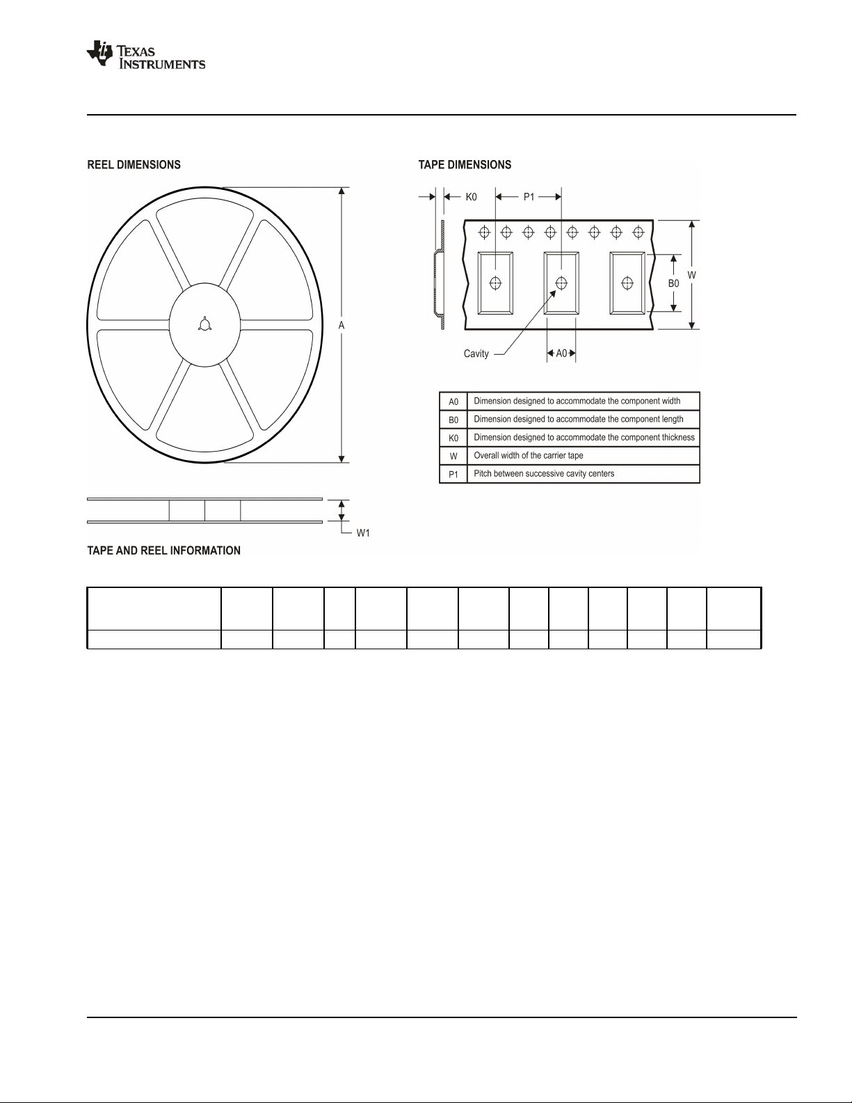
TAPE AND REEL INFORMATION
*All dimensions are nominal
Device Package
Type
TPS43000PWR TSSOP PW 16 2000 330.0 12.4 6.9 5.6 1.6 8.0 12.0 Q1
Package
Drawing
Pins SPQ Reel
Diameter
(mm)
Reel
Width
W1 (mm)
A0
(mm)B0(mm)K0(mm)P1(mm)W(mm)
Pin1
Quadrant
Pack Materials-Page 1
Page 29
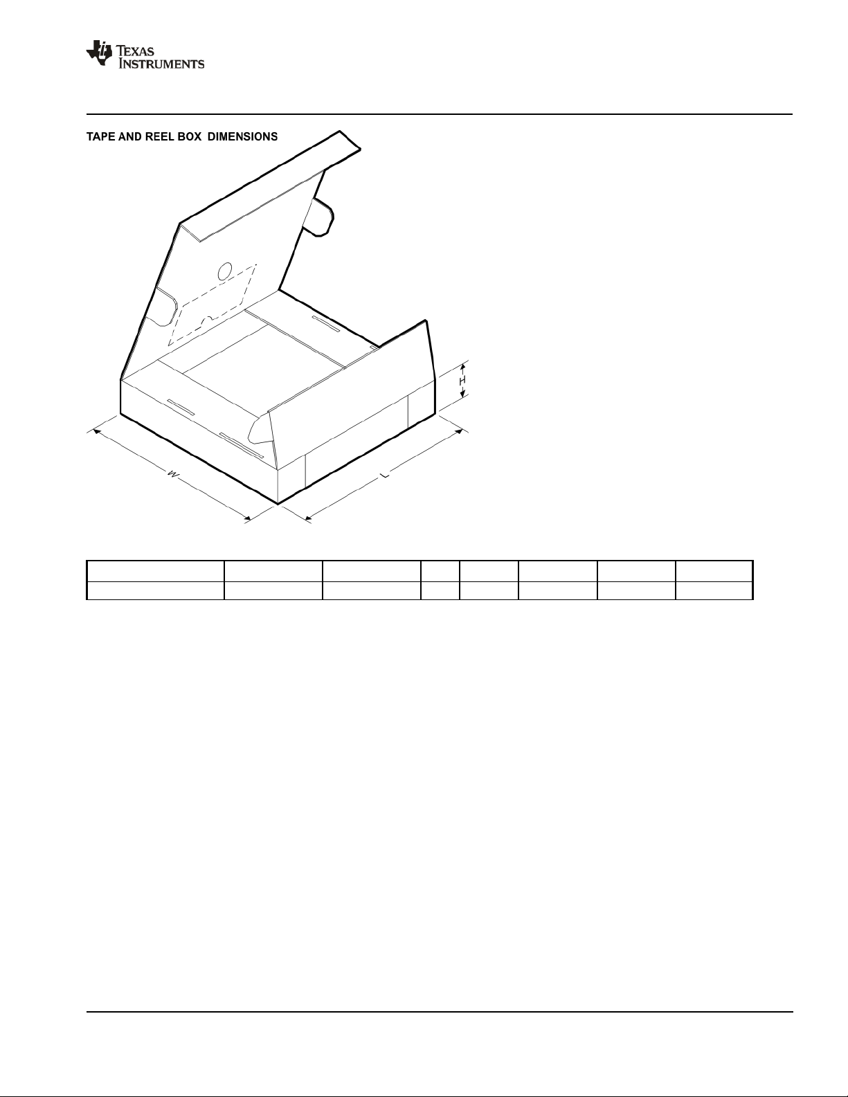
PACKAGE MATERIALS INFORMATION
www.ti.com 14-Jul-2012
*All dimensions are nominal
Device Package Type Package Drawing Pins SPQ Length (mm) Width (mm) Height (mm)
TPS43000PWR TSSOP PW 16 2000 367.0 367.0 35.0
Pack Materials-Page 2
Page 30
Page 31

Page 32

IMPORTANT NOTICE
Texas Instruments Incorporated and its subsidiaries (TI) reserve the right to make corrections, enhancements, improvements and other
changes to its semiconductor products and services per JESD46, latest issue, and to discontinue any product or service per JESD48, latest
issue. Buyers should obtain the latest relevant information before placing orders and should verify that such information is current and
complete. All semiconductor products (also referred to herein as “components”) are sold subject to TI’s terms and conditions of sale
supplied at the time of order acknowledgment.
TI warrants performance of its components to the specifications applicable at the time of sale, in accordance with the warranty in TI’s terms
and conditions of sale of semiconductor products. Testing and other quality control techniques are used to the extent TI deems necessary
to support this warranty. Except where mandated by applicable law, testing of all parameters of each component is not necessarily
performed.
TI assumes no liability for applications assistance or the design of Buyers’ products. Buyers are responsible for their products and
applications using TI components. To minimize the risks associated with Buyers’ products and applications, Buyers should provide
adequate design and operating safeguards.
TI does not warrant or represent that any license, either express or implied, is granted under any patent right, copyright, mask work right, or
other intellectual property right relating to any combination, machine, or process in which TI components or services are used. Information
published by TI regarding third-party products or services does not constitute a license to use such products or services or a warranty or
endorsement thereof. Use of such information may require a license from a third party under the patents or other intellectual property of the
third party, or a license from TI under the patents or other intellectual property of TI.
Reproduction of significant portions of TI information in TI data books or data sheets is permissible only if reproduction is without alteration
and is accompanied by all associated warranties, conditions, limitations, and notices. TI is not responsible or liable for such altered
documentation. Information of third parties may be subject to additional restrictions.
Resale of TI components or services with statements different from or beyond the parameters stated by TI for that component or service
voids all express and any implied warranties for the associated TI component or service and is an unfair and deceptive business practice.
TI is not responsible or liable for any such statements.
Buyer acknowledges and agrees that it is solely responsible for compliance with all legal, regulatory and safety-related requirements
concerning its products, and any use of TI components in its applications, notwithstanding any applications-related information or support
that may be provided by TI. Buyer represents and agrees that it has all the necessary expertise to create and implement safeguards which
anticipate dangerous consequences of failures, monitor failures and their consequences, lessen the likelihood of failures that might cause
harm and take appropriate remedial actions. Buyer will fully indemnify TI and its representatives against any damages arising out of the use
of any TI components in safety-critical applications.
In some cases, TI components may be promoted specifically to facilitate safety-related applications. With such components, TI’s goal is to
help enable customers to design and create their own end-product solutions that meet applicable functional safety standards and
requirements. Nonetheless, such components are subject to these terms.
No TI components are authorized for use in FDA Class III (or similar life-critical medical equipment) unless authorized officers of the parties
have executed a special agreement specifically governing such use.
Only those TI components which TI has specifically designated as military grade or “enhanced plastic” are designed and intended for use in
military/aerospace applications or environments. Buyer acknowledges and agrees that any military or aerospace use of TI components
which have not been so designated is solely at the Buyer's risk, and that Buyer is solely responsible for compliance with all legal and
regulatory requirements in connection with such use.
TI has specifically designated certain components as meeting ISO/TS16949 requirements, mainly for automotive use. In any case of use of
non-designated products, TI will not be responsible for any failure to meet ISO/TS16949.
Products Applications
Audio www.ti.com/audio Automotive and Transportation www.ti.com/automotive
Amplifiers amplifier.ti.com Communications and Telecom www.ti.com/communications
Data Converters dataconverter.ti.com Computers and Peripherals www.ti.com/computers
DLP® Products www.dlp.com Consumer Electronics www.ti.com/consumer-apps
DSP dsp.ti.com Energy and Lighting www.ti.com/energy
Clocks and Timers www.ti.com/clocks Industrial www.ti.com/industrial
Interface interface.ti.com Medical www.ti.com/medical
Logic logic.ti.com Security www.ti.com/security
Power Mgmt power.ti.com Space, Avionics and Defense www.ti.com/space-avionics-defense
Microcontrollers microcontroller.ti.com Video and Imaging www.ti.com/video
RFID www.ti-rfid.com
OMAP Applications Processors www.ti.com/omap TI E2E Community e2e.ti.com
Wireless Connectivity www.ti.com/wirelessconnectivity
Mailing Address: Texas Instruments, Post Office Box 655303, Dallas, Texas 75265
Copyright © 2015, Texas Instruments Incorporated
Page 33

 Loading...