

Page 1

TPS40345EVM-353 Evaluation Module
The TPS40345EVM-353 evaluation module (EVM) is a synchronous buck converter providing a fixed
1.2-V output at up to 20 A from a 12-V input bus. The EVM is designed to start-up from a single supply,
which means no additional bias voltage is required for start-up. The module uses the TPS40345 highperformance, mid-input voltage synchronous buck controller and TI’s NexFET™ high performance
MOSFETs.
Contents
1 Description.................................................................................................................... 3
1.1 Applications.......................................................................................................... 3
1.2 Features.............................................................................................................. 3
2 TPS40345EVM-353 Electrical Performance Specifications............................................................ 3
3 TPS40345EVM-353 Schematic............................................................................................ 4
4 Connector and Test Point Descriptions................................................................................... 5
4.1 Enable Jumper (JP2)............................................................................................... 5
4.2 Frequency Spread Spectrum – FSS Jumper (JP1) ............................................................ 5
4.3 Test Point Descriptions ............................................................................................ 5
5 Test Setup .................................................................................................................... 7
5.1 Equipment ........................................................................................................... 7
5.2 Equipment Setup.................................................................................................... 7
5.3 Start-Up/Shutdown Procedure .................................................................................... 9
5.4 Output Ripple Voltage Measurement Procedure ............................................................... 9
5.5 Control Loop Gain and Phase Measurement Procedure...................................................... 9
5.6 Equipment Shutdown ............................................................................................. 10
6 TPS40345EVM-353 Test Data ........................................................................................... 10
6.1 Efficiency ........................................................................................................... 10
6.2 Line and Load Regulation........................................................................................ 11
6.3 Output Voltage Ripple ............................................................................................ 11
6.4 Switch Node........................................................................................................ 12
6.5 Control Loop Bode Diagram ..................................................................................... 12
6.6 Additional Waveforms ............................................................................................ 13
7 TPS40345EVM-353 Assembly Drawings and Layout................................................................. 13
8 TPS40345EVM-353 Bill of Materials..................................................................................... 17
User's Guide
SNVU588–November 2017
1 TPS40345EVM-353 Schematic............................................................................................ 4
2 TPS40345EVM-353 Recommended Test Set-Up....................................................................... 8
3 Output Ripple Measurement – Tip and Barrel using TP3 and TP4................................................... 8
4 Control Loop Measurement Setup......................................................................................... 9
5 TPS40345EVM-353 Efficiency vs Load Current ....................................................................... 10
6 TPS40345EVM-353 Output Voltage vs Load Current................................................................. 11
7 TPS40345EVM-353 Output Voltage Ripple ............................................................................ 11
8 TPS40345EVM-353 Switching Waveforms............................................................................. 12
9 TPS40345EVM-353 Gain and Phase vs Frequency .................................................................. 12
10 TPS40345EVM-353 Output Ripple With FSS Enabled ............................................................... 13
11 TPS40345EVM-353 Component Placement (Top View) ............................................................. 14
SNVU588–November 2017
Submit Documentation Feedback
List of Figures
Copyright © 2017, Texas Instruments Incorporated
TPS40345EVM-353 Evaluation Module
1
Page 2

12 TPS40345EVM-353 Silk Screen (Top View) ........................................................................... 14
13 TPS40345EVM-353 Top Copper (Top View)........................................................................... 15
14 TPS40345EVM-353 Bottom Copper (Top View)....................................................................... 15
15 TPS40345EVM-353 Internal 1 (X-Ray Top View) ..................................................................... 16
16 TPS40345EVM-353 Internal 2 (X-Ray Top View) ..................................................................... 16
1 TPS40345EVM-353 Electrical and Performance Specifications ...................................................... 3
2 Test Point Descriptions ..................................................................................................... 5
3 TPS40345EVM-353 Bill of Materials..................................................................................... 17
Trademarks
NexFET is a trademark of Texas Instruments.
All other trademarks are the property of their respective owners.
www.ti.com
List of Tables
2
TPS40345EVM-353 Evaluation Module
Copyright © 2017, Texas Instruments Incorporated
SNVU588–November 2017
Submit Documentation Feedback
Page 3
www.ti.com
1 Description
The TPS40345EVM-353 is designed to use a regulated 12 V (8 V – 14 V) bus voltage to provide a
regulated 1.2-V output at up to 20 A of load current. The TPS40345EVM-353 is designed to demonstrate
the TPS40345 controller and TI NexFETs in a typical 12-V bus to low-voltage application while providing a
number of non-invasive test points to evaluate the performance of the TPS40345 and TI NexFETs in a
given application.
1.1 Applications
• High-current, low-voltage FPGA or microcontroller core supplies
• High-current point of load modules
• Telecommunications equipment
• Computer peripherals
1.2 Features
• 8-V to 14-V input voltage rating
• 1.2-V ± 2% output voltage rating
• 20-A steady state load current
• 600-kHz switching frequency
• Simple access to IC features including power good, enable, soft start, and error amplifier
• Convenient test points for simple, non-invasive measurements of converter performance
Description
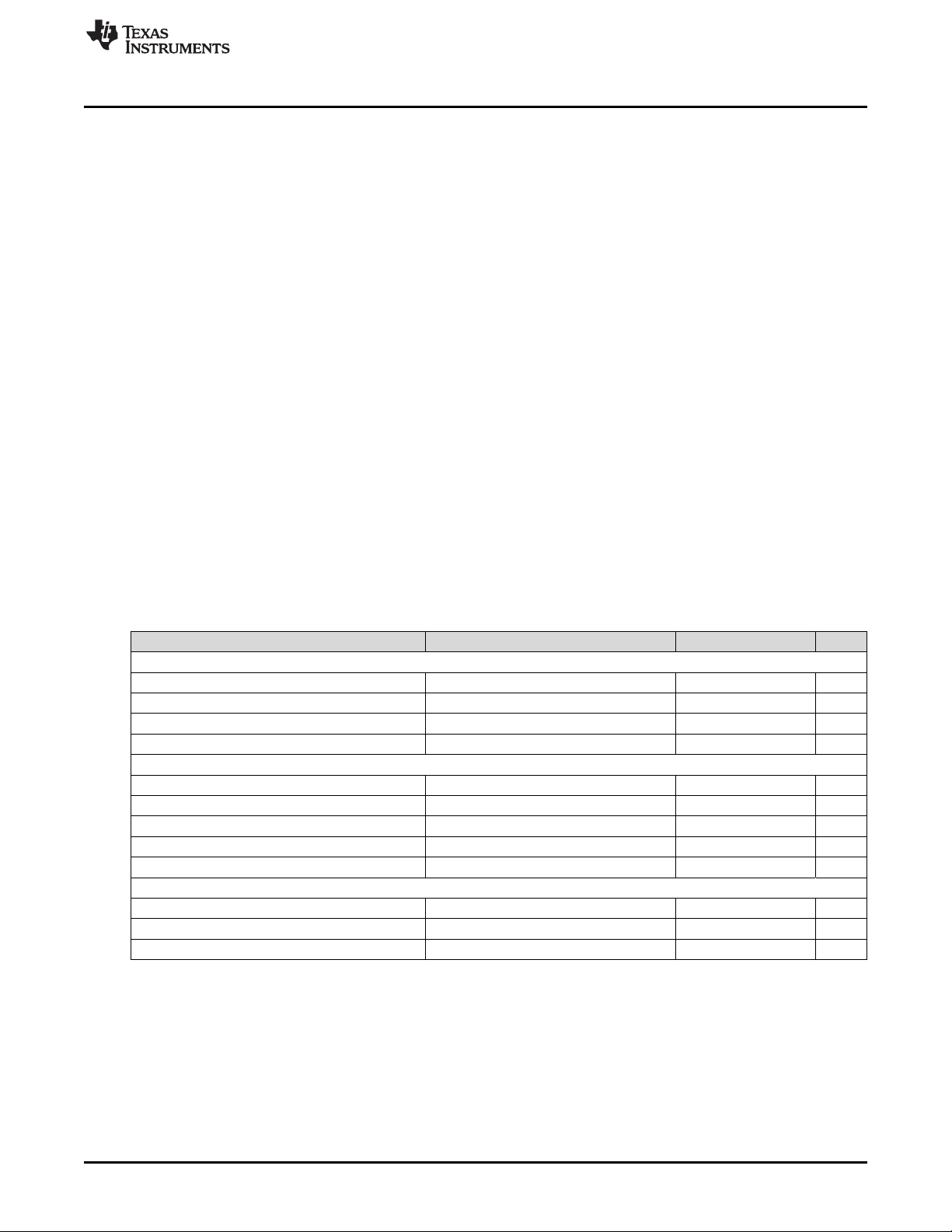
2 TPS40345EVM-353 Electrical Performance Specifications
Table 1. TPS40345EVM-353 Electrical and Performance Specifications
PARAMETER NOTES AND CONDITIONS MIN TYP MAX UNIT
INPUTS CHARACTERISTICS
V
IN
I
IN
V
IN_UVLO
OUTPUTS CHARACTERISTICS
V
OUT1
V
OUT_ripple
I
OUT1
SYSTEMS CHARACTERISTICS
f
SW
ηpk Peak efficiency VIN= 12 V 88%
η Full load efficiency VIN= 12 V, I
Input voltage 8 12 14 V
Input current VIN= Nom, I
No load input current VIN= Nom, I
Input UVLO I
Output voltage 1 VIN= 12 V, I
Line regulation VIN= 8 V to 14 V 0.5%
Load regulation I
Output voltage ripple VIN= 12 V, I
Output current 1 VIN= 8 V to 14 V 0 20 A
Switching frequency 540 600 660 kHz
= 10 A 3.0 V
OUT
= 0 A to 20 A 0.5%
OUT
= Max 2.3 2.5 A
OUT
= 0A 40 50 mA
OUT
= 20 A 1.17 1.2 1.23 V
OUT
= 20 A 24 mVpp
OUT
= 20 A 86%
OUT
SNVU588–November 2017
Submit Documentation Feedback
Copyright © 2017, Texas Instruments Incorporated
TPS40345EVM-353 Evaluation Module
3
Page 4
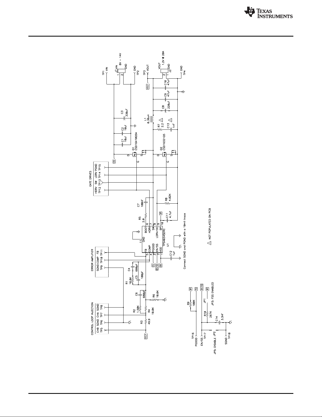
+
+
TPS40345EVM-353 Schematic
3 TPS40345EVM-353 Schematic
www.ti.com
For reference only, See Table 3 for specific values
Figure 1. TPS40345EVM-353 Schematic
4
TPS40345EVM-353 Evaluation Module
Copyright © 2017, Texas Instruments Incorporated
SNVU588–November 2017
Submit Documentation Feedback
Page 5

www.ti.com
4 Connector and Test Point Descriptions
4.1 Enable Jumper (JP2)
The TPS40345EVM-353 is designed with a Disable Jumper (JP2) using a 0.1-inch spacing header and
shunt. Installing a shunt in the JP2 position connects the EN/SS pin to GND, discharges the soft-start
capacitor, and disables the TPS40304 controller. This forces the output into a high-impedance state
(approximately 20kΩ to GND).
4.2 Frequency Spread Spectrum – FSS Jumper (JP1)
The TPS40345EVM-353 is designed with a frequency spread spectrum (FSS) enable jumper (JP1) using
a 0.1" spacing header and shunt. Installing a shunt in the JP1 position connects the EN/SS pin to BP via a
267-kΩ resistor (R10) to enable frequency spread spectrum.
FSS modulates the switching frequency to ±10% of the nominal value at 30 kHz to reduce EMI at the
switching frequency and its harmonics, however there may be a 30-kHz component to the output ripple
(see Figure 10).
The TPS40345EVM-353 does not dynamically monitor the JP1 status for programming FSS. The
TPS40345EVM-353 must be disabled via JP2 or powered down by reducing VIN to less than 3 V to
remove or install JP1.
4.3 Test Point Descriptions
Connector and Test Point Descriptions
Table 2. Test Point Descriptions
TEST
POINT
TP1 VIN Measurement test point for input voltage 4.3.1
TP2 GND Ground test point for input voltage 4.3.1
TP3 VOUT Measurement test point for output voltage 4.3.1
TP4 GND Ground test point for output voltage 4.3.2
TP5 CHB Measurement test point for channel B of loop response 4.3.3
TP6 SGND Ground test point for channel B of loop response 4.3.3
TP7 CHA Measurement test point for channel A of loop response 4.3.3
TP8 SGND Ground test point for channel A of loop response 4.3.3
TP9 SGND Ground test point for error amplifier measurements 4.3.4
TP10 COMP Measurement test point for error amplifier output voltage 4.3.4
TP11 FB Measurement test point for error amplifier input voltage 4.3.4
TP12 HDRV Measurement test point for high-side gate driver voltage 4.3.5
TP13 SW Measurement test point for switching node voltage 4.3.5
TP14 LDRV Measurement test point for low-side gate driver voltage 4.3.5
TP15 PGND Ground test point for switch node and gate drive voltages 4.3.5
TP16 PGOOD Measurement test point for power good 4.3.6
TP17 EN/SS Measurement test point for enable / soft start 4.3.7
TP18 SGND Ground test point for power good and enable / soft start 4.3.6 and 4.3.7
LABEL USE SECTION
SNVU588–November 2017
Submit Documentation Feedback
Copyright © 2017, Texas Instruments Incorporated
TPS40345EVM-353 Evaluation Module
5
Page 6

Connector and Test Point Descriptions
4.3.1 Input Voltage Monitoring (TP1 and TP2)
The TPS40345EVM-353 provides two test points for measuring the input voltage applied to the module.
This allows the user to measure the actual input module voltage without losses from input cables and
connectors. All input voltage measurements should be made between TP1 and TP2. To use TP1 and
TP2, connect a voltmeter positive input to TP1 and input terminal to TP2.
4.3.2 Output Voltage Monitoring (TP3 and TP4)
The TPS40345EVM-353 provides two test points for measuring the output voltage generated by the
module. This allows the user to measure the actual module output voltage without losses from input
cables and connectors. All input voltage measurements should be made between TP3 and TP4. To use
TP3 and TP4, connect a voltmeter positive input to TP3 and negative input to TP4.
4.3.3 Loop Response Testing (TP5, TP6, TP7, TP8, and R3)
The TPS40345EVM-353 provides four test points (2 signal and 2 ground) for measuring the control loop
frequency response. This allows the user to measure the actual module loop response without modifying
the evaluation board. A transformer isolated signal up to 30 mV can be injected between TP5 and TP7.
The injected signal amplitude can be measured by the ac coupled amplitude at CHA (TP7) and the
resulting output voltage deviation can be measured at CHB (TP5). See Figure 4 for additional detail.
4.3.4 Error Amplifier Voltage Monitoring (TP9, TP10, and TP11)
The TPS40345EVM-353 provides three test points for measuring the error amplifier input and output
voltages. This allows the user to directly measure the feedback and control voltages of the TPS40304
controller. The control voltage (TP10) can also be used to measure the control to output or power-stage
frequency response or output to control or error amplifier frequency response. See Section 5.5 for
additional details.
www.ti.com
4.3.5 Switching Waveform Monitoring (TP12, TP13, TP14, and TP15)
The TPS40345EVM-353 provides three test points and a local power ground for measuring the switching
waveforms of the module power stage. This allows the user to monitor actual switching waveforms during
operation. TP13 is a 0.040-inch square pad of exposed PCB copper to minimize EMI radiation from the
high transient voltages on the switch node. Switching waveform measurements should be made using
power ground (TP15) as the ground reference for more accurate measurements.
4.3.6 Power-Good Voltage Monitoring (TP16 and TP18)
The TPS40345EVM-353 provides a test point and local ground for measuring the power good output
voltage. A 100-kΩ resistor pullup to BP (R9) is included to allow the power-good signal to be monitored
without requiring an external pull-up. For true open-drain operation with no pullup, remove R9. With R9
removed, TP16 can be connected to TP17 of another TPS40345EVM-353 to provide sequential start-up of
the two TPS40345EVM-353 converters.
4.3.7 Enable and Soft-Start Voltage Monitoring (TP17 and TP18)
The TPS40345EVM-353 provides a test point and local ground for measuring the enable and soft-start
voltage. TP17 and TP18 or JP2 can be used to provide an external enable signal. Due to the nature of the
soft-start function, the external signal must be open-collector or open-drain without pullup.
6
TPS40345EVM-353 Evaluation Module
Copyright © 2017, Texas Instruments Incorporated
SNVU588–November 2017
Submit Documentation Feedback
Page 7

www.ti.com
5 Test Setup
5.1 Equipment
5.1.1 Voltage Source
VIN— The input voltage source (VIN) must be a 0-V to 15-V variable DC source capable of supplying 5
Adc.
5.1.2 Meters
A1: — Input current meter. 0 Adc – 5 Adc ammeter
V1: — Input voltage meter. 0 V – 15 V voltmeter
V2: — Output voltage meter. 0 V – 2 V voltmeter
5.1.3 Load
LOAD1: — Output load. Electronic load set for constant current or constant resistance capable of 0 Adc –
20 Adc at 1.2-Vdc.
5.1.4 Oscilloscope
For output voltage ripple: — Oscilloscope must be an analog or digital oscilloscope set for ac-coupled
measurement with 20-MHz bandwidth limiting. Use 20 mV/division vertical resolution, 1-µs/division
horizontal resolution.
For switching waveforms: — Oscilloscope shall be an analog or digital oscilloscope set for dc coupled
measurement with 20-MHz bandwidth limiting. Use 2 V/division or 5V/division vertical resolution and 1µs/division horizontal resolution.
Test Setup
5.1.5 Recommended Wire Gauge
VIN to J1: — The connection between the source voltage (VIN) and J1 of TPS40345EVM-353 can carry as
much as 3.5 Adc of current. The minimum recommended wire size is AWG #16 with the total length of
wire less than 2 feet (1 foot input, 1 foot return).
J2 to LOAD1: — The connection between the source voltage (VIN) and J1 of TPS40345EVM-353 can
carry as much as 20 Adc of current. The minimum recommended wire size is AWG #12 with the total
length of wire less than 2 feet (1 foot input, 1 foot return).
5.1.6 Other
FAN: — The TPS40345EVM-353 evaluation module includes components that can get hot to the touch
when operating. Because this evaluation module is not enclosed to allow probing of circuit nodes, TI
recommends a small fan capable of 200 lfm – 400 lfm to reduce component temperatures when operating.
5.2 Equipment Setup
Shown in Figure 2 is the basic test set up recommended to evaluate the TPS40345EVM-353. Note that
although the return for J1 and JP2 are the same system ground, the connections should remain separate
as shown in Figure 2.
5.2.1 Procedure
1. Working at an ESD workstation, make sure that any wrist straps, bootstraps, or mats are connected
referencing the user to earth ground before power is applied to the EVM. Electrostatic smock and
safety glasses should also be worn.
2. Prior to connecting the dc input source, VIN, it is advisable to limit the source current from VINto 4 A,
maximum. Make sure VINis initially set to 0 V and connected as shown in Figure 2.
3. Connect VIN to J1 as shown in Figure 2.
SNVU588–November 2017
Submit Documentation Feedback
Copyright © 2017, Texas Instruments Incorporated
TPS40345EVM-353 Evaluation Module
7
Page 8

TP4TP3
MetalGroundBarrel
Probe Tip
TipandBarrelVoutripple
measurement
LOAD1
1.2V @
20A
+
-
FAN
V2
-
+
See Tip and Barrel
Measurement for
Vout ripple
V1
+
-
A1
-
+
V
IN
Oscilloscope
1MW, AC
20mV / div
20MHz
Test Setup
4. Connect ammeter A1 between VIN and J1 as shown in Figure 2.
5. Connect voltmeter V1 to TP1 and TP2 as shown in Figure 2.
6. Connect voltmeter V2 to TP3 and TP4 as shown in Figure 2.
7. Connect oscilloscope probes to desired test points per Table 2.
8. Place fan as shown in Figure 2 and turn on making sure to blow air directly across the evaluation
module.
5.2.2 Diagram
www.ti.com
8
TPS40345EVM-353 Evaluation Module
Figure 2. TPS40345EVM-353 Recommended Test Set-Up
Figure 3. Output Ripple Measurement – Tip and Barrel using TP3 and TP4
Copyright © 2017, Texas Instruments Incorporated
SNVU588–November 2017
Submit Documentation Feedback
Page 9

Network
Analyzer
Isolation
Transformer
LOAD1
1.2V @
20A
+
-
V2
-
+
See Tip and Barrel
Measurement for
Vout ripple
V1
+
-
A1
-
+
V
IN
Oscilloscope
1MW, AC
20mV / div
20MHz
www.ti.com
Test Setup
Figure 4. Control Loop Measurement Setup
5.3 Start-Up/Shutdown Procedure
1. Verify shunt position for JP1 for desired FSS status per _________(need correct reference).
2. Remove shunt from JP2 location if present.
3. Increase VINfrom 0 Vdc to 12 Vdc.
4. Vary LOAD1 from 0 Adc to 20 Adc.
5. Vary VINfrom 8 V to 14 V.
6. Decrease VINto 0 V.
7. Decrease LOAD1 to 0 A.
5.4 Output Ripple Voltage Measurement Procedure
1. Follow Section 5.3 steps 1 – 5 to set VINand LOAD1 to the desired operating condition.
2. Connect oscilloscope probe with exposed metal barrel to TP3 and TP4 per Figure 3.
3. Set oscilloscope per oscilloscope for output voltage ripple measurement in Section 5.1.4.
4. Follow Section 5.3 steps 6 and 7 to power down.
5.5 Control Loop Gain and Phase Measurement Procedure
1. Follow Section 5.3 steps 1 – 5 to set VINand LOAD1 to the desired operating condition:
SNVU588–November 2017
Submit Documentation Feedback
a. If JP1 is installed (FSS enabled), loop response data about the modulation frequency (30 kHz)
may be affected.
2. Connect a 1-kHz – 1-MHz isolation transformer to TP5 and TP7 as shown in Figure 4.
Copyright © 2017, Texas Instruments Incorporated
TPS40345EVM-353 Evaluation Module
9
Page 10

0 5 10 15 20
I -LoadCurrent- A
L
8V
12V
14V
60
65
70
75
80
85
90
95
h -Efficiency-%
Channel B
20 LOG
Channel A
æ ö
´
ç ÷
è ø
Test Setup
3. Connect input signal amplitude measurement probe (channel A) to TP7 as shown in Figure 4.
4. Connect output signal amplitude measurement probe (channel B) to TP5 as shown in Figure 4.
5. Connect ground lead of channel A and channel B to TP6 and TP8 as shown in Figure 4.
6. Inject 30 mV or less signal across R3 through isolation transformer.
7. Sweep frequency from 1 kHz to 1 MHz with 10-Hz or lower post filter.
8. Control loop gain can be measured by
9. Control loop phase can be measured by the phase difference between channel A and channel B.
10. Control to output response (power stage transfer function) can be measured by connecting channel A
probe to TP10 (COMP) and channel B probe to TP5 (CHB).
11. Output to control response (compensated error amplifier transfer function) can be measured by
connecting channel A probe to TP7 (CHA) and channel B probe to TP10 (COMP).
12. Follow Section 5.3 steps 6 and 7 to power down.
5.6 Equipment Shutdown
1. Shut down oscilloscope
2. Shut down LOAD1
3. Shut down V
4. Shut down fan
IN
www.ti.com
6 TPS40345EVM-353 Test Data
Figure 5 through Figure 10 present typical performance curves for the TPS40345EVM-353. Since actual
performance data can be affected by measurement techniques and environmental variables, these curves
are presented for reference and may differ from actual field measurements.
6.1 Efficiency
10
VIN= 8.0V – 14V, V
OUT
= 1.2V, I
OUT
Figure 5. TPS40345EVM-353 Efficiency vs Load Current
TPS40345EVM-353 Evaluation Module
= 0A – 20A
Copyright © 2017, Texas Instruments Incorporated
SNVU588–November 2017
Submit Documentation Feedback
Page 11

Vin = 14V, Vout = 1.2 V, Iout = 20 A
Output Ripple
1.188
1.191
1.194
1.197
1.2
1.203
1.206
1.209
1.212
0 5 10 15 20 25
V -OutputVoltage-V
O
I -LoadCurrent- A
L
8V
12V
14V
www.ti.com
6.2 Line and Load Regulation
TPS40345EVM-353 Test Data
VIN= 8.0V – 14V, V
6.3 Output Voltage Ripple
OUT
= 1.2V, I
= 0A – 20A
OUT
Figure 6. TPS40345EVM-353 Output Voltage vs Load Current
OUT
= 1.2V, I
= 20A
OUT
Figure 7. TPS40345EVM-353 Output Voltage Ripple
VIN= 14V, V
SNVU588–November 2017
Submit Documentation Feedback
Copyright © 2017, Texas Instruments Incorporated
TPS40345EVM-353 Evaluation Module
11
Page 12

-60
-40
-20
0
20
40
60
80
100
0.1 1 10 100 1000
f-Frequency-kHz
-135
-90
-45
0
45
90
135
180
225
Gain
Phase
Gain-dB
Vin = 14V, Vout = 1.2 V, Iout = 20 A
Switching
TPS40345EVM-353 Test Data
6.4 Switch Node
www.ti.com
6.5 Control Loop Bode Diagram
VIN= 12V, V
OUT
= 1.2V, I
OUT
= 20 A
Ch1: TP12 (HDRV), Ch2:13 TP (SW), Ch3: TP14 (LDRV)
Figure 8. TPS40345EVM-353 Switching Waveforms
VIN= 14V, V
OUT
= 1.2V, I
= 20A, Bandwidth: 73kHz, Phase Margin: 47°
OUT
Figure 9. TPS40345EVM-353 Gain and Phase vs Frequency
12
TPS40345EVM-353 Evaluation Module
Copyright © 2017, Texas Instruments Incorporated
SNVU588–November 2017
Submit Documentation Feedback
Page 13

Vin = 14V, Vout = 1.2 V, Iout = 20 A
Output Ripple
www.ti.com
6.6 Additional Waveforms
6.6.1 Output Ripple With Frequency Spread Spectrum (FSS) Enabled
FSS varies the output switching frequency. This change in switching frequency can produce a small
change in the output voltage at the modulation frequency. Figure 10 shows the approximately 10-mV
modulation of the output voltage generated when FSS is enabled.
TPS40345EVM-353 Test Data
7 TPS40345EVM-353 Assembly Drawings and Layout
The following figures (Figure 11 through Figure 16) show the design of the TPS40345EVM-353 printed
circuit board. The EVM has been designed using a 4-layer, 2-oz. copper-clad circuit board 3-inch × 3-inch
with all components on the top to allow the user to easily view, probe, and evaluate the TPSxxxxx control
IC in a practical double-sided application. Moving components to both sides of the PCB or using additional
internal layers can offer additional size reduction for space constrained systems.
Figure 10. TPS40345EVM-353 Output Ripple With FSS Enabled
SNVU588–November 2017
Submit Documentation Feedback
Copyright © 2017, Texas Instruments Incorporated
TPS40345EVM-353 Evaluation Module
13
Page 14

TPS40345EVM-353 Assembly Drawings and Layout
Figure 11. TPS40345EVM-353 Component Placement (Top View)
www.ti.com
14
Figure 12. TPS40345EVM-353 Silk Screen (Top View)
TPS40345EVM-353 Evaluation Module
Copyright © 2017, Texas Instruments Incorporated
SNVU588–November 2017
Submit Documentation Feedback
Page 15

www.ti.com
TPS40345EVM-353 Assembly Drawings and Layout
Figure 13. TPS40345EVM-353 Top Copper (Top View)
SNVU588–November 2017
Submit Documentation Feedback
Figure 14. TPS40345EVM-353 Bottom Copper (Top View)
TPS40345EVM-353 Evaluation Module
Copyright © 2017, Texas Instruments Incorporated
15
Page 16

TPS40345EVM-353 Assembly Drawings and Layout
Figure 15. TPS40345EVM-353 Internal 1 (X-Ray Top View)
www.ti.com
16
Figure 16. TPS40345EVM-353 Internal 2 (X-Ray Top View)
TPS40345EVM-353 Evaluation Module
Copyright © 2017, Texas Instruments Incorporated
SNVU588–November 2017
Submit Documentation Feedback
Page 17

www.ti.com
TPS40345EVM-353 Bill of Materials
8 TPS40345EVM-353 Bill of Materials
Table 3. TPS40345EVM-353 Bill of Materials
QTY RefDes Value Description Size Part Number MFR
2 C1, C2 10µF Capacitor, Ceramic, 25V, X7R, 10% 1210 Std Std
1 C11 4.7µF Capacitor, Ceramic, 10V, X7R, 20% 0805 Std Std
1 C12 1µF Capacitor, Ceramic, 25V, X7R, 20% 0805 Std Std
0 C13 1nF Capacitor, Ceramic, 25V, X5R, 20% 0603 Std Std
1 C14 3.3nF Capacitor, Ceramic, 16V, X7R, 20% 0603 Std Std
1 C3 330µF Capacitor,Aluminum, 25V, ±20%, 160mΩ 0.328 x 0.390 inch EEEFK1E331P Panasonic
2 C4, C6 680pF Capacitor, Ceramic, 25V, COG, 10% 0603 Std Std
1 C5 100pF Capacitor, Ceramic, 25V, COG, 10% 0603 Std Std
1 C7 100nF Capacitor, Ceramic, 16V, X7R, 20% 0603 Std Std
1 C8 220µF Capacitor, POSCAP, 6.3V, 25mΩ, 105C, 20% 7343(D) 6TPE220M Sanyo
2 C9, C10 47µF Capacitor, Ceramic, 6.3V, X5R, 20% 1210 Std Std
2 J1, J2 ED120/2DS Terminal Block, 2-pin, 15A, 5.1mm 0.40 x 0.35 inch ED120/2DS OST
2 JP1, JP2 PEC02SAAN Header, 2-pin, 100mil spacing 0.100 inch x 2 PEC02SAAN Sullins
1 L1 0.38µH Inductor, SMT, 35A 0.512 x 0.571 inch PG0077.401NLT Pulse
1 Q1* CSD16410Q5A MOSFET, N-Chan, 25V, 59A, 9.6mΩ QFN-8 POWER CSD16410Q5A TI
1 Q2* CSD16321Q5 MOSFET, N-Chan, 25V, 31A QFN-8 POWER CSD16321Q5 TI
3 R1, R4, R6 10.0kΩ Resistor, Chip, 1/16W, 1% 0603 Std Std
1 R10 267kΩ Resistor, Chip, 1/16W, 1% 0603 Std Std
1 R2 1.50kΩ Resistor, Chip, 1/16W, 1% 0603 Std Std
1 R3 49.9Ω Resistor, Chip, 1/16W, 1% 0603 Std Std
1 R5 2Ω Resistor, Chip, 1/16W, 1% 0603 Std Std
0 R7 2.2Ω Resistor, Chip, 1/8W, 5% 1206 Std Std
1 R8 4.02kΩ Resistor, Chip, 1/16W, 1% 0603 Std Std
1 R9 100kΩ Resistor, Chip, 1/16W, 1% 0603 Std Std
2 TP1, TP3 5000 Test Point, Red, Thru Hole Color Keyed 0.100 x 0.100 inch 5000 Keystone
0 TP13 N/A Test Point, SM, 2x3mm 0.118 x 0.079 inch
6 TP2, TP4, TP6,
TP8, TP15, TP18
9 TP5, TP7,
TP9–TP12, TP14,
TP16, TP17
1 U1* TPS40345DRC IC, 3V – 20V sync. Buck controller/Enable Light Load/Fq
2 – Shunt, 100-mil, Black 0.1 929950-00 3M
1 – PCB, 2.5 In x 2.5 In x 0.062 In HPA353 Any
5001 Test Point, Black, Thru Hole Color Keyed 0.100 x 0.100 inch 5001 Keystone
5002 Test Point, White, Thru Hole Color Keyed 0.100 x 0.100 inch 5002 Keystone
Spread Spectrum
DRC10 TPS40345DRC TI
SNVU588–November 2017
Submit Documentation Feedback
Copyright © 2017, Texas Instruments Incorporated
TPS40345EVM-353 Evaluation Module
17
Page 18

Evaluation Board/Kit Important Notice
Texas Instruments (TI) provides the enclosed product(s) under the following conditions:
This evaluation board/kit is intended for use for ENGINEERING DEVELOPMENT, DEMONSTRATION, OR EVALUATION PURPOSES
ONLY and is not considered by TI to be a finished end-product fit for general consumer use. Persons handling the product(s) must have
electronics training and observe good engineering practice standards. As such, the goods being provided are not intended to be complete
in terms of required design-, marketing-, and/or manufacturing-related protective considerations, including product safety and environmental
measures typically found in end products that incorporate such semiconductor components or circuit boards. This evaluation board/kit does
not fall within the scope of the European Union directives regarding electromagnetic compatibility, restricted substances (RoHS), recycling
(WEEE), FCC, CE or UL, and therefore may not meet the technical requirements of these directives or other related directives.
Should this evaluation board/kit not meet the specifications indicated in the User’s Guide, the board/kit may be returned within 30 days from
the date of delivery for a full refund. THE FOREGOING WARRANTY IS THE EXCLUSIVE WARRANTY MADE BY SELLER TO BUYER
AND IS IN LIEU OF ALL OTHER WARRANTIES, EXPRESSED, IMPLIED, OR STATUTORY, INCLUDING ANY WARRANTY OF
MERCHANTABILITY OR FITNESS FOR ANY PARTICULAR PURPOSE.
The user assumes all responsibility and liability for proper and safe handling of the goods. Further, the user indemnifies TI from all claims
arising from the handling or use of the goods. Due to the open construction of the product, it is the user’s responsibility to take any and all
appropriate precautions with regard to electrostatic discharge.
EXCEPT TO THE EXTENT OF THE INDEMNITY SET FORTH ABOVE, NEITHER PARTY SHALL BE LIABLE TO THE OTHER FOR ANY
INDIRECT, SPECIAL, INCIDENTAL, OR CONSEQUENTIAL DAMAGES.
TI currently deals with a variety of customers for products, and therefore our arrangement with the user is not exclusive.
TI assumes no liability for applications assistance, customer product design, software performance, or infringement of patents or
services described herein.
Please read the User’s Guide and, specifically, the Warnings and Restrictions notice in the User’s Guide prior to handling the product. This
notice contains important safety information about temperatures and voltages. For additional information on TI’s environmental and/or
safety programs, please contact the TI application engineer or visit www.ti.com/esh.
No license is granted under any patent right or other intellectual property right of TI covering or relating to any machine, process, or
combination in which such TI products or services might be or are used.
FCC Warning
This evaluation board/kit is intended for use for ENGINEERING DEVELOPMENT, DEMONSTRATION, OR EVALUATION PURPOSES
ONLY and is not considered by TI to be a finished end-product fit for general consumer use. It generates, uses, and can radiate radio
frequency energy and has not been tested for compliance with the limits of computing devices pursuant to part 15 of FCC rules, which are
designed to provide reasonable protection against radio frequency interference. Operation of this equipment in other environments may
cause interference with radio communications, in which case the user at his own expense will be required to take whatever measures may
be required to correct this interference.
EVM Warnings and Restrictions
It is important to operate this EVM within the input voltage range of and the output voltage range of .
Exceeding the specified input range may cause unexpected operation and/or irreversible damage to the EVM. If there are questions
concerning the input range, please contact a TI field representative prior to connecting the input power.
Applying loads outside of the specified output range may result in unintended operation and/or possible permanent damage to the EVM.
Please consult the EVM User's Guide prior to connecting any load to the EVM output. If there is uncertainty as to the load specification,
please contact a TI field representative.
During normal operation, some circuit components may have case temperatures greater than . The EVM is designed to operate properly
with certain components above as long as the input and output ranges are maintained. These components include but are not limited to
linear regulators, switching transistors, pass transistors, and current sense resistors. These types of devices can be identified using the
EVM schematic located in the EVM User's Guide. When placing measurement probes near these devices during operation, please be
aware that these devices may be very warm to the touch.
Mailing Address: Texas Instruments, Post Office Box 655303, Dallas, Texas 75265
Copyright © 2017, Texas Instruments Incorporated
Page 19

STANDARD TERMS FOR EVALUATION MODULES
1. Delivery: TI delivers TI evaluation boards, kits, or modules, including any accompanying demonstration software, components, and/or
documentation which may be provided together or separately (collectively, an “EVM” or “EVMs”) to the User (“User”) in accordance
with the terms set forth herein. User's acceptance of the EVM is expressly subject to the following terms.
1.1 EVMs are intended solely for product or software developers for use in a research and development setting to facilitate feasibility
evaluation, experimentation, or scientific analysis of TI semiconductors products. EVMs have no direct function and are not
finished products. EVMs shall not be directly or indirectly assembled as a part or subassembly in any finished product. For
clarification, any software or software tools provided with the EVM (“Software”) shall not be subject to the terms and conditions
set forth herein but rather shall be subject to the applicable terms that accompany such Software
1.2 EVMs are not intended for consumer or household use. EVMs may not be sold, sublicensed, leased, rented, loaned, assigned,
or otherwise distributed for commercial purposes by Users, in whole or in part, or used in any finished product or production
system.
2 Limited Warranty and Related Remedies/Disclaimers:
2.1 These terms do not apply to Software. The warranty, if any, for Software is covered in the applicable Software License
Agreement.
2.2 TI warrants that the TI EVM will conform to TI's published specifications for ninety (90) days after the date TI delivers such EVM
to User. Notwithstanding the foregoing, TI shall not be liable for a nonconforming EVM if (a) the nonconformity was caused by
neglect, misuse or mistreatment by an entity other than TI, including improper installation or testing, or for any EVMs that have
been altered or modified in any way by an entity other than TI, (b) the nonconformity resulted from User's design, specifications
or instructions for such EVMs or improper system design, or (c) User has not paid on time. Testing and other quality control
techniques are used to the extent TI deems necessary. TI does not test all parameters of each EVM.
User's claims against TI under this Section 2 are void if User fails to notify TI of any apparent defects in the EVMs within ten (10)
business days after delivery, or of any hidden defects with ten (10) business days after the defect has been detected.
2.3 TI's sole liability shall be at its option to repair or replace EVMs that fail to conform to the warranty set forth above, or credit
User's account for such EVM. TI's liability under this warranty shall be limited to EVMs that are returned during the warranty
period to the address designated by TI and that are determined by TI not to conform to such warranty. If TI elects to repair or
replace such EVM, TI shall have a reasonable time to repair such EVM or provide replacements. Repaired EVMs shall be
warranted for the remainder of the original warranty period. Replaced EVMs shall be warranted for a new full ninety (90) day
warranty period.
3 Regulatory Notices:
3.1 United States
3.1.1 Notice applicable to EVMs not FCC-Approved:
FCC NOTICE: This kit is designed to allow product developers to evaluate electronic components, circuitry, or software
associated with the kit to determine whether to incorporate such items in a finished product and software developers to write
software applications for use with the end product. This kit is not a finished product and when assembled may not be resold or
otherwise marketed unless all required FCC equipment authorizations are first obtained. Operation is subject to the condition
that this product not cause harmful interference to licensed radio stations and that this product accept harmful interference.
Unless the assembled kit is designed to operate under part 15, part 18 or part 95 of this chapter, the operator of the kit must
operate under the authority of an FCC license holder or must secure an experimental authorization under part 5 of this chapter.
3.1.2 For EVMs annotated as FCC – FEDERAL COMMUNICATIONS COMMISSION Part 15 Compliant:
CAUTION
This device complies with part 15 of the FCC Rules. Operation is subject to the following two conditions: (1) This device may not
cause harmful interference, and (2) this device must accept any interference received, including interference that may cause
undesired operation.
Changes or modifications not expressly approved by the party responsible for compliance could void the user's authority to
operate the equipment.
FCC Interference Statement for Class A EVM devices
NOTE: This equipment has been tested and found to comply with the limits for a Class A digital device, pursuant to part 15 of
the FCC Rules. These limits are designed to provide reasonable protection against harmful interference when the equipment is
operated in a commercial environment. This equipment generates, uses, and can radiate radio frequency energy and, if not
installed and used in accordance with the instruction manual, may cause harmful interference to radio communications.
Operation of this equipment in a residential area is likely to cause harmful interference in which case the user will be required to
correct the interference at his own expense.
Page 20

FCC Interference Statement for Class B EVM devices
NOTE: This equipment has been tested and found to comply with the limits for a Class B digital device, pursuant to part 15 of
the FCC Rules. These limits are designed to provide reasonable protection against harmful interference in a residential
installation. This equipment generates, uses and can radiate radio frequency energy and, if not installed and used in accordance
with the instructions, may cause harmful interference to radio communications. However, there is no guarantee that interference
will not occur in a particular installation. If this equipment does cause harmful interference to radio or television reception, which
can be determined by turning the equipment off and on, the user is encouraged to try to correct the interference by one or more
of the following measures:
• Reorient or relocate the receiving antenna.
• Increase the separation between the equipment and receiver.
• Connect the equipment into an outlet on a circuit different from that to which the receiver is connected.
• Consult the dealer or an experienced radio/TV technician for help.
3.2 Canada
3.2.1 For EVMs issued with an Industry Canada Certificate of Conformance to RSS-210 or RSS-247
Concerning EVMs Including Radio Transmitters:
This device complies with Industry Canada license-exempt RSSs. Operation is subject to the following two conditions:
(1) this device may not cause interference, and (2) this device must accept any interference, including interference that may
cause undesired operation of the device.
Concernant les EVMs avec appareils radio:
Le présent appareil est conforme aux CNR d'Industrie Canada applicables aux appareils radio exempts de licence. L'exploitation
est autorisée aux deux conditions suivantes: (1) l'appareil ne doit pas produire de brouillage, et (2) l'utilisateur de l'appareil doit
accepter tout brouillage radioélectrique subi, même si le brouillage est susceptible d'en compromettre le fonctionnement.
Concerning EVMs Including Detachable Antennas:
Under Industry Canada regulations, this radio transmitter may only operate using an antenna of a type and maximum (or lesser)
gain approved for the transmitter by Industry Canada. To reduce potential radio interference to other users, the antenna type
and its gain should be so chosen that the equivalent isotropically radiated power (e.i.r.p.) is not more than that necessary for
successful communication. This radio transmitter has been approved by Industry Canada to operate with the antenna types
listed in the user guide with the maximum permissible gain and required antenna impedance for each antenna type indicated.
Antenna types not included in this list, having a gain greater than the maximum gain indicated for that type, are strictly prohibited
for use with this device.
Concernant les EVMs avec antennes détachables
Conformément à la réglementation d'Industrie Canada, le présent émetteur radio peut fonctionner avec une antenne d'un type et
d'un gain maximal (ou inférieur) approuvé pour l'émetteur par Industrie Canada. Dans le but de réduire les risques de brouillage
radioélectrique à l'intention des autres utilisateurs, il faut choisir le type d'antenne et son gain de sorte que la puissance isotrope
rayonnée équivalente (p.i.r.e.) ne dépasse pas l'intensité nécessaire à l'établissement d'une communication satisfaisante. Le
présent émetteur radio a été approuvé par Industrie Canada pour fonctionner avec les types d'antenne énumérés dans le
manuel d’usage et ayant un gain admissible maximal et l'impédance requise pour chaque type d'antenne. Les types d'antenne
non inclus dans cette liste, ou dont le gain est supérieur au gain maximal indiqué, sont strictement interdits pour l'exploitation de
l'émetteur
3.3 Japan
3.3.1 Notice for EVMs delivered in Japan: Please see http://www.tij.co.jp/lsds/ti_ja/general/eStore/notice_01.page 日本国内に
輸入される評価用キット、ボードについては、次のところをご覧ください。
http://www.tij.co.jp/lsds/ti_ja/general/eStore/notice_01.page
3.3.2 Notice for Users of EVMs Considered “Radio Frequency Products” in Japan: EVMs entering Japan may not be certified
by TI as conforming to Technical Regulations of Radio Law of Japan.
If User uses EVMs in Japan, not certified to Technical Regulations of Radio Law of Japan, User is required to follow the
instructions set forth by Radio Law of Japan, which includes, but is not limited to, the instructions below with respect to EVMs
(which for the avoidance of doubt are stated strictly for convenience and should be verified by User):
1. Use EVMs in a shielded room or any other test facility as defined in the notification #173 issued by Ministry of Internal
Affairs and Communications on March 28, 2006, based on Sub-section 1.1 of Article 6 of the Ministry’s Rule for
Enforcement of Radio Law of Japan,
2. Use EVMs only after User obtains the license of Test Radio Station as provided in Radio Law of Japan with respect to
EVMs, or
3. Use of EVMs only after User obtains the Technical Regulations Conformity Certification as provided in Radio Law of Japan
with respect to EVMs. Also, do not transfer EVMs, unless User gives the same notice above to the transferee. Please note
that if User does not follow the instructions above, User will be subject to penalties of Radio Law of Japan.
Page 21

【無線電波を送信する製品の開発キットをお使いになる際の注意事項】 開発キットの中には技術基準適合証明を受けて
いないものがあります。 技術適合証明を受けていないもののご使用に際しては、電波法遵守のため、以下のいずれかの
措置を取っていただく必要がありますのでご注意ください。
1. 電波法施行規則第6条第1項第1号に基づく平成18年3月28日総務省告示第173号で定められた電波暗室等の試験設備でご使用
いただく。
2. 実験局の免許を取得後ご使用いただく。
3. 技術基準適合証明を取得後ご使用いただく。
なお、本製品は、上記の「ご使用にあたっての注意」を譲渡先、移転先に通知しない限り、譲渡、移転できないものとします。
上記を遵守頂けない場合は、電波法の罰則が適用される可能性があることをご留意ください。 日本テキサス・イ
ンスツルメンツ株式会社
東京都新宿区西新宿6丁目24番1号
西新宿三井ビル
3.3.3 Notice for EVMs for Power Line Communication: Please see http://www.tij.co.jp/lsds/ti_ja/general/eStore/notice_02.page
電力線搬送波通信についての開発キットをお使いになる際の注意事項については、次のところをご覧ください。http:/
/www.tij.co.jp/lsds/ti_ja/general/eStore/notice_02.page
3.4 European Union
3.4.1 For EVMs subject to EU Directive 2014/30/EU (Electromagnetic Compatibility Directive):
This is a class A product intended for use in environments other than domestic environments that are connected to a
low-voltage power-supply network that supplies buildings used for domestic purposes. In a domestic environment this
product may cause radio interference in which case the user may be required to take adequate measures.
4 EVM Use Restrictions and Warnings:
4.1 EVMS ARE NOT FOR USE IN FUNCTIONAL SAFETY AND/OR SAFETY CRITICAL EVALUATIONS, INCLUDING BUT NOT
LIMITED TO EVALUATIONS OF LIFE SUPPORT APPLICATIONS.
4.2 User must read and apply the user guide and other available documentation provided by TI regarding the EVM prior to handling
or using the EVM, including without limitation any warning or restriction notices. The notices contain important safety information
related to, for example, temperatures and voltages.
4.3 Safety-Related Warnings and Restrictions:
4.3.1 User shall operate the EVM within TI’s recommended specifications and environmental considerations stated in the user
guide, other available documentation provided by TI, and any other applicable requirements and employ reasonable and
customary safeguards. Exceeding the specified performance ratings and specifications (including but not limited to input
and output voltage, current, power, and environmental ranges) for the EVM may cause personal injury or death, or
property damage. If there are questions concerning performance ratings and specifications, User should contact a TI
field representative prior to connecting interface electronics including input power and intended loads. Any loads applied
outside of the specified output range may also result in unintended and/or inaccurate operation and/or possible
permanent damage to the EVM and/or interface electronics. Please consult the EVM user guide prior to connecting any
load to the EVM output. If there is uncertainty as to the load specification, please contact a TI field representative.
During normal operation, even with the inputs and outputs kept within the specified allowable ranges, some circuit
components may have elevated case temperatures. These components include but are not limited to linear regulators,
switching transistors, pass transistors, current sense resistors, and heat sinks, which can be identified using the
information in the associated documentation. When working with the EVM, please be aware that the EVM may become
very warm.
4.3.2 EVMs are intended solely for use by technically qualified, professional electronics experts who are familiar with the
dangers and application risks associated with handling electrical mechanical components, systems, and subsystems.
User assumes all responsibility and liability for proper and safe handling and use of the EVM by User or its employees,
affiliates, contractors or designees. User assumes all responsibility and liability to ensure that any interfaces (electronic
and/or mechanical) between the EVM and any human body are designed with suitable isolation and means to safely
limit accessible leakage currents to minimize the risk of electrical shock hazard. User assumes all responsibility and
liability for any improper or unsafe handling or use of the EVM by User or its employees, affiliates, contractors or
designees.
4.4 User assumes all responsibility and liability to determine whether the EVM is subject to any applicable international, federal,
state, or local laws and regulations related to User’s handling and use of the EVM and, if applicable, User assumes all
responsibility and liability for compliance in all respects with such laws and regulations. User assumes all responsibility and
liability for proper disposal and recycling of the EVM consistent with all applicable international, federal, state, and local
requirements.
5. Accuracy of Information: To the extent TI provides information on the availability and function of EVMs, TI attempts to be as accurate
as possible. However, TI does not warrant the accuracy of EVM descriptions, EVM availability or other information on its websites as
accurate, complete, reliable, current, or error-free.
Page 22

6. Disclaimers:
6.1 EXCEPT AS SET FORTH ABOVE, EVMS AND ANY MATERIALS PROVIDED WITH THE EVM (INCLUDING, BUT NOT
LIMITED TO, REFERENCE DESIGNS AND THE DESIGN OF THE EVM ITSELF) ARE PROVIDED "AS IS" AND "WITH ALL
FAULTS." TI DISCLAIMS ALL OTHER WARRANTIES, EXPRESS OR IMPLIED, REGARDING SUCH ITEMS, INCLUDING BUT
NOT LIMITED TO ANY EPIDEMIC FAILURE WARRANTY OR IMPLIED WARRANTIES OF MERCHANTABILITY OR FITNESS
FOR A PARTICULAR PURPOSE OR NON-INFRINGEMENT OF ANY THIRD PARTY PATENTS, COPYRIGHTS, TRADE
SECRETS OR OTHER INTELLECTUAL PROPERTY RIGHTS.
6.2 EXCEPT FOR THE LIMITED RIGHT TO USE THE EVM SET FORTH HEREIN, NOTHING IN THESE TERMS SHALL BE
CONSTRUED AS GRANTING OR CONFERRING ANY RIGHTS BY LICENSE, PATENT, OR ANY OTHER INDUSTRIAL OR
INTELLECTUAL PROPERTY RIGHT OF TI, ITS SUPPLIERS/LICENSORS OR ANY OTHER THIRD PARTY, TO USE THE
EVM IN ANY FINISHED END-USER OR READY-TO-USE FINAL PRODUCT, OR FOR ANY INVENTION, DISCOVERY OR
IMPROVEMENT, REGARDLESS OF WHEN MADE, CONCEIVED OR ACQUIRED.
7. USER'S INDEMNITY OBLIGATIONS AND REPRESENTATIONS. USER WILL DEFEND, INDEMNIFY AND HOLD TI, ITS
LICENSORS AND THEIR REPRESENTATIVES HARMLESS FROM AND AGAINST ANY AND ALL CLAIMS, DAMAGES, LOSSES,
EXPENSES, COSTS AND LIABILITIES (COLLECTIVELY, "CLAIMS") ARISING OUT OF OR IN CONNECTION WITH ANY
HANDLING OR USE OF THE EVM THAT IS NOT IN ACCORDANCE WITH THESE TERMS. THIS OBLIGATION SHALL APPLY
WHETHER CLAIMS ARISE UNDER STATUTE, REGULATION, OR THE LAW OF TORT, CONTRACT OR ANY OTHER LEGAL
THEORY, AND EVEN IF THE EVM FAILS TO PERFORM AS DESCRIBED OR EXPECTED.
8. Limitations on Damages and Liability:
8.1 General Limitations. IN NO EVENT SHALL TI BE LIABLE FOR ANY SPECIAL, COLLATERAL, INDIRECT, PUNITIVE,
INCIDENTAL, CONSEQUENTIAL, OR EXEMPLARY DAMAGES IN CONNECTION WITH OR ARISING OUT OF THESE
TERMS OR THE USE OF THE EVMS , REGARDLESS OF WHETHER TI HAS BEEN ADVISED OF THE POSSIBILITY OF
SUCH DAMAGES. EXCLUDED DAMAGES INCLUDE, BUT ARE NOT LIMITED TO, COST OF REMOVAL OR
REINSTALLATION, ANCILLARY COSTS TO THE PROCUREMENT OF SUBSTITUTE GOODS OR SERVICES, RETESTING,
OUTSIDE COMPUTER TIME, LABOR COSTS, LOSS OF GOODWILL, LOSS OF PROFITS, LOSS OF SAVINGS, LOSS OF
USE, LOSS OF DATA, OR BUSINESS INTERRUPTION. NO CLAIM, SUIT OR ACTION SHALL BE BROUGHT AGAINST TI
MORE THAN TWELVE (12) MONTHS AFTER THE EVENT THAT GAVE RISE TO THE CAUSE OF ACTION HAS
OCCURRED.
8.2 Specific Limitations. IN NO EVENT SHALL TI'S AGGREGATE LIABILITY FROM ANY USE OF AN EVM PROVIDED
HEREUNDER, INCLUDING FROM ANY WARRANTY, INDEMITY OR OTHER OBLIGATION ARISING OUT OF OR IN
CONNECTION WITH THESE TERMS, , EXCEED THE TOTAL AMOUNT PAID TO TI BY USER FOR THE PARTICULAR
EVM(S) AT ISSUE DURING THE PRIOR TWELVE (12) MONTHS WITH RESPECT TO WHICH LOSSES OR DAMAGES ARE
CLAIMED. THE EXISTENCE OF MORE THAN ONE CLAIM SHALL NOT ENLARGE OR EXTEND THIS LIMIT.
9. Return Policy. Except as otherwise provided, TI does not offer any refunds, returns, or exchanges. Furthermore, no return of EVM(s)
will be accepted if the package has been opened and no return of the EVM(s) will be accepted if they are damaged or otherwise not in
a resalable condition. If User feels it has been incorrectly charged for the EVM(s) it ordered or that delivery violates the applicable
order, User should contact TI. All refunds will be made in full within thirty (30) working days from the return of the components(s),
excluding any postage or packaging costs.
10. Governing Law: These terms and conditions shall be governed by and interpreted in accordance with the laws of the State of Texas,
without reference to conflict-of-laws principles. User agrees that non-exclusive jurisdiction for any dispute arising out of or relating to
these terms and conditions lies within courts located in the State of Texas and consents to venue in Dallas County, Texas.
Notwithstanding the foregoing, any judgment may be enforced in any United States or foreign court, and TI may seek injunctive relief
in any United States or foreign court.
Mailing Address: Texas Instruments, Post Office Box 655303, Dallas, Texas 75265
Copyright © 2017, Texas Instruments Incorporated
Page 23

IMPORTANT NOTICE FOR TI DESIGN INFORMATION AND RESOURCES
Texas Instruments Incorporated (‘TI”) technical, application or other design advice, services or information, including, but not limited to,
reference designs and materials relating to evaluation modules, (collectively, “TI Resources”) are intended to assist designers who are
developing applications that incorporate TI products; by downloading, accessing or using any particular TI Resource in any way, you
(individually or, if you are acting on behalf of a company, your company) agree to use it solely for this purpose and subject to the terms of
this Notice.
TI’s provision of TI Resources does not expand or otherwise alter TI’s applicable published warranties or warranty disclaimers for TI
products, and no additional obligations or liabilities arise from TI providing such TI Resources. TI reserves the right to make corrections,
enhancements, improvements and other changes to its TI Resources.
You understand and agree that you remain responsible for using your independent analysis, evaluation and judgment in designing your
applications and that you have full and exclusive responsibility to assure the safety of your applications and compliance of your applications
(and of all TI products used in or for your applications) with all applicable regulations, laws and other applicable requirements. You
represent that, with respect to your applications, you have all the necessary expertise to create and implement safeguards that (1)
anticipate dangerous consequences of failures, (2) monitor failures and their consequences, and (3) lessen the likelihood of failures that
might cause harm and take appropriate actions. You agree that prior to using or distributing any applications that include TI products, you
will thoroughly test such applications and the functionality of such TI products as used in such applications. TI has not conducted any
testing other than that specifically described in the published documentation for a particular TI Resource.
You are authorized to use, copy and modify any individual TI Resource only in connection with the development of applications that include
the TI product(s) identified in such TI Resource. NO OTHER LICENSE, EXPRESS OR IMPLIED, BY ESTOPPEL OR OTHERWISE TO
ANY OTHER TI INTELLECTUAL PROPERTY RIGHT, AND NO LICENSE TO ANY TECHNOLOGY OR INTELLECTUAL PROPERTY
RIGHT OF TI OR ANY THIRD PARTY IS GRANTED HEREIN, including but not limited to any patent right, copyright, mask work right, or
other intellectual property right relating to any combination, machine, or process in which TI products or services are used. Information
regarding or referencing third-party products or services does not constitute a license to use such products or services, or a warranty or
endorsement thereof. Use of TI Resources may require a license from a third party under the patents or other intellectual property of the
third party, or a license from TI under the patents or other intellectual property of TI.
TI RESOURCES ARE PROVIDED “AS IS” AND WITH ALL FAULTS. TI DISCLAIMS ALL OTHER WARRANTIES OR
REPRESENTATIONS, EXPRESS OR IMPLIED, REGARDING TI RESOURCES OR USE THEREOF, INCLUDING BUT NOT LIMITED TO
ACCURACY OR COMPLETENESS, TITLE, ANY EPIDEMIC FAILURE WARRANTY AND ANY IMPLIED WARRANTIES OF
MERCHANTABILITY, FITNESS FOR A PARTICULAR PURPOSE, AND NON-INFRINGEMENT OF ANY THIRD PARTY INTELLECTUAL
PROPERTY RIGHTS.
TI SHALL NOT BE LIABLE FOR AND SHALL NOT DEFEND OR INDEMNIFY YOU AGAINST ANY CLAIM, INCLUDING BUT NOT
LIMITED TO ANY INFRINGEMENT CLAIM THAT RELATES TO OR IS BASED ON ANY COMBINATION OF PRODUCTS EVEN IF
DESCRIBED IN TI RESOURCES OR OTHERWISE. IN NO EVENT SHALL TI BE LIABLE FOR ANY ACTUAL, DIRECT, SPECIAL,
COLLATERAL, INDIRECT, PUNITIVE, INCIDENTAL, CONSEQUENTIAL OR EXEMPLARY DAMAGES IN CONNECTION WITH OR
ARISING OUT OF TI RESOURCES OR USE THEREOF, AND REGARDLESS OF WHETHER TI HAS BEEN ADVISED OF THE
POSSIBILITY OF SUCH DAMAGES.
You agree to fully indemnify TI and its representatives against any damages, costs, losses, and/or liabilities arising out of your noncompliance with the terms and provisions of this Notice.
This Notice applies to TI Resources. Additional terms apply to the use and purchase of certain types of materials, TI products and services.
These include; without limitation, TI’s standard terms for semiconductor products http://www.ti.com/sc/docs/stdterms.htm), evaluation
modules, and samples (http://www.ti.com/sc/docs/sampterms.htm).
Mailing Address: Texas Instruments, Post Office Box 655303, Dallas, Texas 75265
Copyright © 2017, Texas Instruments Incorporated
 Loading...