

5
4
3
2
6
7
8
9
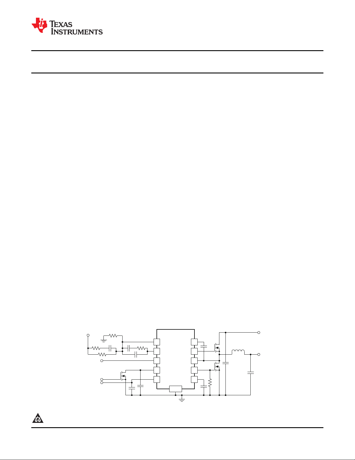
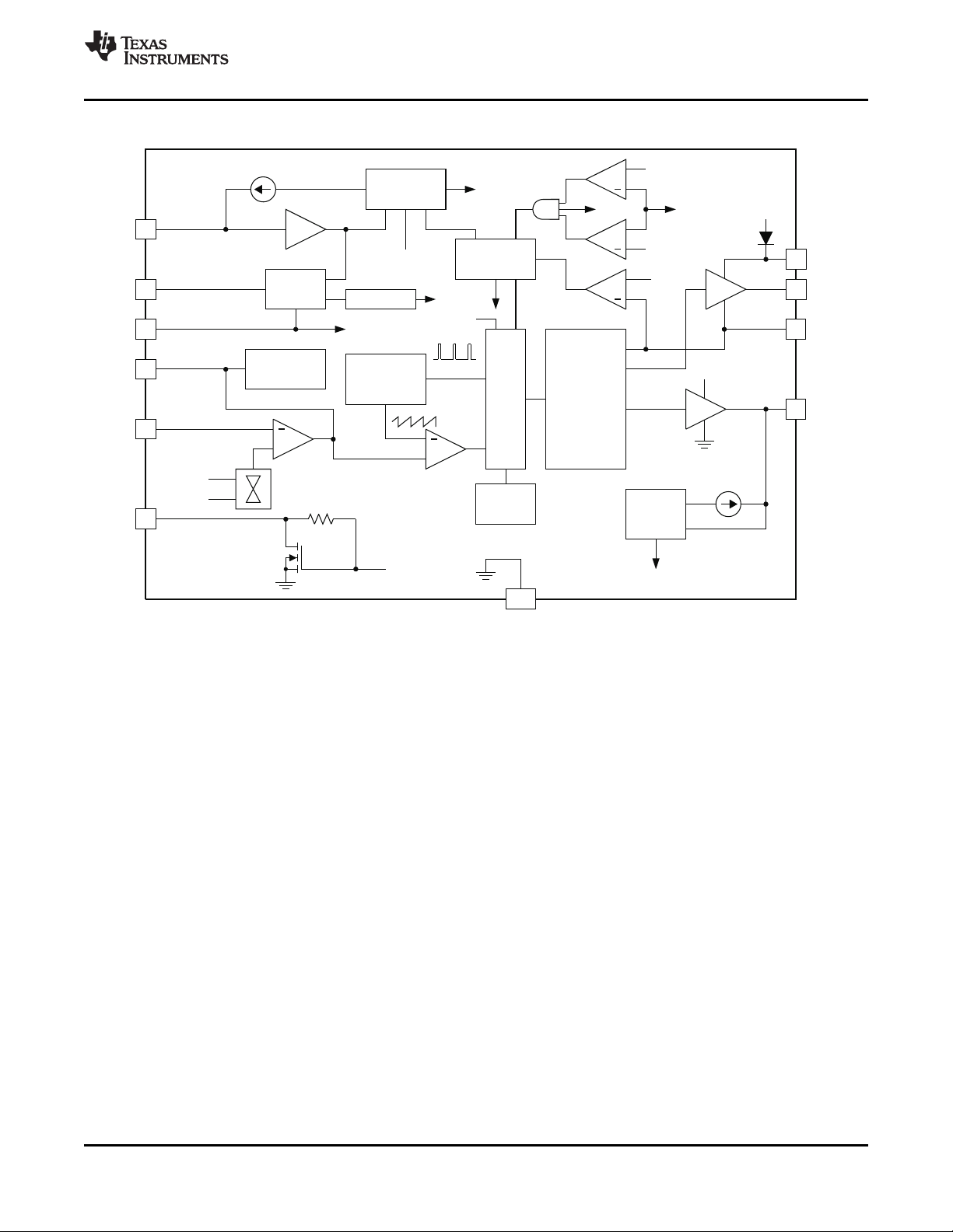
BOOT
HDRV
SW
LDRV/OC
FB
COMP
PGOOD
EN/SS
TPS4030x
1 10BPVDD
PAD
V
IN
SD
V
OUT
V
IN
UDG-09158
V
OUT
GND
www.ti.com
TPS40303, TPS40304, TPS40305
SLUS964 –NOVEMBER 2009
3-V TO 20-V INPUT SYNCHRONOUS BUCK CONTROLLER
Check for Samples :TPS40303 TPS40304 TPS40305
1
FEATURES
• Input Voltage Range from 3 V to 20 V
• 300 KHz (TPS40303), 600 KHz (TPS40304) and
1.2 MHz (TPS40305) Switching Frequencies
• High- and Low-Side FET R
DS(on)
Current
Sensing
• Programmable Thermally Compensated OCP
Levels
• Programmable Soft-Start
• 600 mV, 1% Reference Voltage
• Voltage Feed-Forward Compensation
• Supports Pre-Biased Output
• Frequency Spread Spectrum
• Thermal Shutdown Protection at 145°C
CONTENTS
Device Ratings 2
Electrical Characteristics 3
Device Information 8
Application Information 10
Design Examples 14
Additional References 24
X
APPLICATIONS
• POL Modules
• Printer
• Digital TV
• Telecom
• 10-Pin 3 mm × 3 mm SON Package with
Ground Connection to Thermal Pad
DESCRIPTION
The TPS4030x is a family of cost-optimized synchronous buck controllers that operate from 3-V to 20-V input.
The controller implements a voltage-mode control architecture with input-voltage feed-forward compensation that
responds instantly to input voltage change. The switching frequency is fixed at 300 KHz, 600 KHz or 1.2 MHz.
Frequency Spread Spectrum feature adds dither to the switching frequency, significantly reducing the peak EMI
noise and making it much easier to comply with EMI standards.
The TPS4030x offers design with a variety of user programmable functions, including soft-start, Over- Current
Protection (OCP) levels, and loop compensation.
OCP level may be programmed by a single external resistor connected from LDRV pin to circuit ground. During
initial power on, the TPS4030x enters a calibration cycle, measures the voltage at the LDRV pin, and sets an
internal OCP voltage level. During operation, the programmed OCP voltage level is compared to the voltage drop
across the low side FET when it is on to determine whether there is an overcurrent condition. The TPS4030x
then enters a shutdown and restart cycle until the fault is removed.
SIMPLIFIED APPLICATION DIAGRAM
1
Please be aware that an important notice concerning availability, standard warranty, and use in critical applications of Texas
Instruments semiconductor products and disclaimers thereto appears at the end of this data sheet.
PRODUCTION DATA information is current as of publication date.
Products conform to specifications per the terms of the Texas
Instruments standard warranty. Production processing does not
necessarily include testing of all parameters.
Copyright © 2009, Texas Instruments Incorporated
TPS40303, TPS40304, TPS40305
SLUS964 –NOVEMBER 2009
This integrated circuit can be damaged by ESD. Texas Instruments recommends that all integrated circuits be handled with
appropriate precautions. Failure to observe proper handling and installation procedures can cause damage.
ESD damage can range from subtle performance degradation to complete device failure. Precision integrated circuits may be more
susceptible to damage because very small parametric changes could cause the device not to meet its published specifications.
ORDERING INFORMATION
OPERATING FREQUENCY PACKAGE TAPE AND REEL QUANTITY PART NUMBER
1.2 MHz
600 kHz Plastic 10-Pin SON (DRC)
300 kHz
250 TPS40305DRCT
3000 TPS40305DRCR
250 TPS40304DRCT
3000 TPS40304DRCR
250 TPS40303DRCT
3000 TPS40303DRCR
www.ti.com
ABSOLUTE MAXIMUM RATINGS
over operating free-air temperature range (unless otherwise noted)
VDD –0.3 to 22 V
SW –3 to 27 V
SW (< 100 ns pulse width, 10 µJ) –5 V
BOOT –0.3 to 30 V
HDRV –5 to 30 V
BOOT-SW, HDRV-SW (differential from BOOT or HDRV to SW) –0.3 to 7 V
COMP, PGOOD, FB, BP, LDRV, EN/SS –0.3 to 7 V
T
Operating junction temperature range –40 to 145 °C
J
T
Storage temperature –55 to 150 °C
stg
(1) Stresses beyond those listed under absolute maximum ratings may cause permanent damage to the device. These are stress ratings
only and functional operation of the device at these or any other condition beyond those included under recommended operating
conditions is not implied. Exposure to absolute-maximum-rated conditions for extended periods of time may affect device reliability.
(1)
VALUE UNIT
DISSIPATION RATINGS
R
HIGH-K BOARD
PACKAGE AIRFLOW (LFM)
0 (Natural Convection) 47.9 2.08 0.835
10-Pin SON (DRC) 200 40.5 2.46 0.987
400 38.2 2.61 1.04
(1) Ratings based on JEDEC High Thermal Conductivity (High K) Board. For more information on the test method, see TI technical brief
(SZZA017).
θJA
(°C/W) TA= 25°C TA= 85°C
(1)
POWER RATING (W) POWER RATING (W)
RECOMMENDED OPERATING CONDITIONS
MIN NOM MAX UNIT
VDD Input voltage 3 20 V
T
Operating junction temperature –40 125 °C
J
ELECTROSTATIC DISCHARGE (ESD) PROTECTION
MIN TYP MAX UNIT
Human body model (HBM) 2000 V
Charge device model (CDM) 1500 V
2 Submit Documentation Feedback Copyright © 2009, Texas Instruments Incorporated
Product Folder Link(s) :TPS40303 TPS40304 TPS40305
www.ti.com
ELECTRICAL CHARACTERISTICS
TJ= –40°C to 125°C, V
PARAMETER TEST CONDITIONS MIN TYP MAX UNIT
VOLTAGE REFERENCE
V
FB
INPUT SUPPLY
V
VDD
IDD
SD
IDD
Q
ENABLE/SOFT-START
V
IH
V
IL
I
SS
V
SS
BP REGULATOR
V
BP
V
DO
OSCILLATOR
f
SW
V
RAMP
f
SWFSS
f
MOD
PWM
(1)
D
MAX
t
ON(min)
t
DEAD
ERROR AMPLIFIER
(1)
G
BWP
(1)
A
OL
I
IB
I
EAOP
I
EAOM
(1) Ensured by design. Not production tested.
FB input voltage mV
Input supply voltage range 3 20 V
Shutdown supply current V
Quiescent, non-switching Let EN/SS float, VFB= 1 V 2.5 3.5 mA
High-level input voltage, EN/SS 0.55 0.70 1.00 V
Low-level input voltage, EN/SS 0.27 0.30 0.33 V
Soft-start source current 8 10 12 µA
Soft-start voltage level 0.4 0.8 1.3 V
Output voltage IBP= 10 mA 6.2 6.5 6.8 V
Regulator dropout voltage, V
PWM frequency TPS40304 3 V < V
(1)
Ramp amplitude V
Frequency spread spectrum frequency
deviation
Modulation frequency 25 KHz
Maximum duty cycle TPS40304 VFB= 0 V, 3 V < V
(1)
Minimum controllable pulse width 100 ns
Output driver dead time ns
Gain bandwidth product 10 24 MHz
Open loop gain 60 dB
Input bias current (current out of FB pin) VFB= 0.6 V 75 nA
Output source current VFB= 0 V 2
Output sink current VFB= 1 V 2
= 12 V, all parameters at zero power dissipation (unless otherwise noted)
VDD
VDD
TPS40303 270 300 330 kHz
TPS40305 1.02 1.20 1.38 MHz
TPS40303 90%
TPS40305 85%
– V
TPS40303, TPS40304, TPS40305
SLUS964 –NOVEMBER 2009
TJ= 25°C, 3 V < V
–40°C < TJ< 125°C, 3 V < V
V
< 0.2 V 70 100 µA
EN/SS
BPIBP
= 25 mA, V
< 20 V 540 600 660 kHz
VDD
HDRV off to LDRV on 5 25 35
LDRV off to HDRV on 5 25 30
< 20 V 597 600 603
VDD
< 20 594 600 606
VDD
= 3 V 70 110 mV
VDD
/6.6 V
VDD
VDD
12% f
< 20 V 90%
VDD
/6 V
/5.4 V
VDD
SW
mA
Copyright © 2009, Texas Instruments Incorporated Submit Documentation Feedback 3
Product Folder Link(s) :TPS40303 TPS40304 TPS40305
TPS40303, TPS40304, TPS40305
SLUS964 –NOVEMBER 2009
ELECTRICAL CHARACTERISTICS (continued)
TJ= –40°C to 125°C, V
PARAMETER TEST CONDITIONS MIN TYP MAX UNIT
PGOOD
V
OV
V
UV
V
PGD-HYST
R
PGD
I
PGDLK
OUTPUT DRIVERS
R
HDHI
R
HDLO
R
LDHI
R
LDLO
(2)
t
HRISE
(2)
t
HFALL
(2)
t
LRISE
(2)
t
LFALL
OVERCURRENT PROTECTION
t
PSSC(min)
t
BLNKH
V
OCH
I
OCSET
V
LD-CLAMP
V
OCLOS
V
OCLPRO
(2)
V
THTC
t
OFF
BOOT DIODE
V
DFWD
THERMAL SHUTDOWN
(2)
T
JSD
(2)
T
JSDH
(2) Ensured by design. Not production tested.
Feedback upper voltage limit for
PGOOD
Feedback lower voltage limit for mV
PGOOD
PGOOD hysteresis voltage at FB 25 40
PGOOD pull down resistance VFB= 0 V, IFB= 5 mA 30 70 Ω
PGOOD leakage current 10 20 µA
High-side driver pull-up resistance V
High-side driver pull-down resistance V
Low-side driver pull-up resistance I
Low-side driver pull-down resistance I
High-side driver rise time C
High-side driver fall time 12 ns
Low-side driver rise time 15 ns
Low-side driver fall time 10 ns
(2)
Minimum pulse time during short circuit 250 ns
(2)
Switch leading-edge blanking pulse time 150 ns
OC threshold for high side FET TJ= 25°C 360 450 580 mV
OCSET current source TJ= 25°C 9.5 10.0 10.5 µA
Maximum clamp voltage at LDRV 260 340 400 mV
OC comparator offset voltage for low
side FET
Programmable OC range for low side
(2)
FET
OC threshold temperature coefficient
(both high side and low side)
OC retry cycles on EN/SS pin 4 Cycle
Bootstrap diode forward voltage I
Junction shutdown temperature 145 °C
Hysteresis 20 °C
= 12 V, all parameters at zero power dissipation (unless otherwise noted)
VDD
550 mV < VFB< 655 mV,
V
PGOOD
BOOT
BOOT
= -100 mA 0.8 1.5 2.5 Ω
LDRV
= 100 mA 0.35 0.60 1.20 Ω
LDRV
LOAD
TJ= 25°C –8 8 mV
TJ= 25°C 12 300 mV
= 5 mA 0.8 V
BOOT
www.ti.com
655 675 700
500 525 550
= 5 V
– VSW= 5 V, I
– VSW= 5 V, I
= –100 mA 0.8 1.5 2.5 Ω
HDRV
= 100 mA 0.5 1.0 2.2 Ω
HDRV
= 5 nF 15 ns
3000 ppm
4 Submit Documentation Feedback Copyright © 2009, Texas Instruments Incorporated
Product Folder Link(s) :TPS40303 TPS40304 TPS40305
305
306
307
308
309
310
311
312
313
314
–40 20–25 –10 5 65 12580 95 11035 50
TJ– Junction Temperature – °C
f
SW
– Switching Frequency – kHz
TPS40303
V
VDD
= 3V
V
VDD
= 12 V
V
VDD
= 20 V
580
585
590
595
600
605
610
615
620
625
V
VDD
= 3V
V
VDD
= 20 V
–40 20–25 –10 5 65 12580 95 11035 50
TJ– Junction Temperature – °C
TPS40304
f
SW
– Switching Frequency – kHz
V
VDD
= 12 V
–40 20–25 –10 5 65 12580 95 11035 50
TJ– Junction Temperature – °C
I
DDQ
– Quiescent Current – mA
2.12
2.14
2.16
2.18
2.20
2.22
2.24
V
VDD
= 12 V
1
1.05
1.1
1.15
1.2
1.25
1.3
1.35
1.4
V
VDD
= 3V
V
VDD
= 20 V
V
VDD
= 12 V
TJ– Junction Temperature – °C
f
SW
– Switching Frequency – MHz
–40 20–25 –10 5 65 12580 95 11035 50
TPS40305
www.ti.com
TPS40303, TPS40304, TPS40305
SLUS964 –NOVEMBER 2009
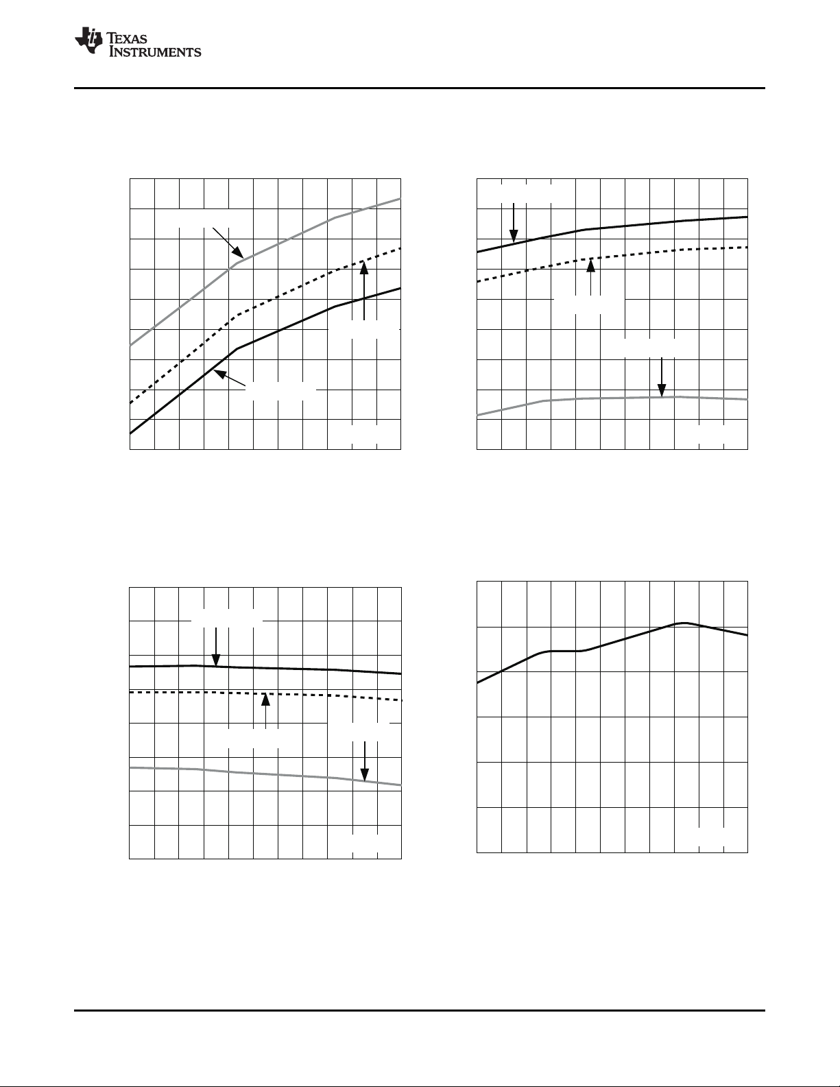
TYPICAL CHARACTERISTICS
SWITCHING FREQUENCY SWITCHING FREQUENCY
vs vs
JUNCTION TEMPERATURE JUNCTION TEMPERATURE
Copyright © 2009, Texas Instruments Incorporated Submit Documentation Feedback 5
Figure 1. Figure 2.
SWITCHING FREQUENCY QUIESCENT CURRENT
vs vs
JUNCTION TEMPERATURE JUNCTION TEMPERATURE
Figure 3. Figure 4.
Product Folder Link(s) :TPS40303 TPS40304 TPS40305
TJ– Junction Temperature – °C
I
DD(SD)
– Shutdown Current – mA
–40 20–25 –10 5 65 12580 95 11035 50
58
60
62
64
66
68
70
72
V
VDD
= 12 V
–40 20–25 –10 5 65 12580 95 11035 50
TJ– Junction Temperature – °C
I
OCSET
– OCSET Current Source– mA
6
7
8
9
10
11
12
13
14
–40 20
599.4
599.6
599.8
600
600.2
600.4
600.6
600.8
–25 –10 5 65 12580 95 11035 50
V
FB
– Feedback Reference Voltage – mV
TJ– Junction Temperature – °C
–40 20–25 –10 5 65 12580 95 11035 50
TJ– Junction Temperature – °C
V
IH
– Enable High-Level Threshold Voltage – mV
620
640
660
680
700
720
740
TPS40303, TPS40304, TPS40305
SLUS964 –NOVEMBER 2009
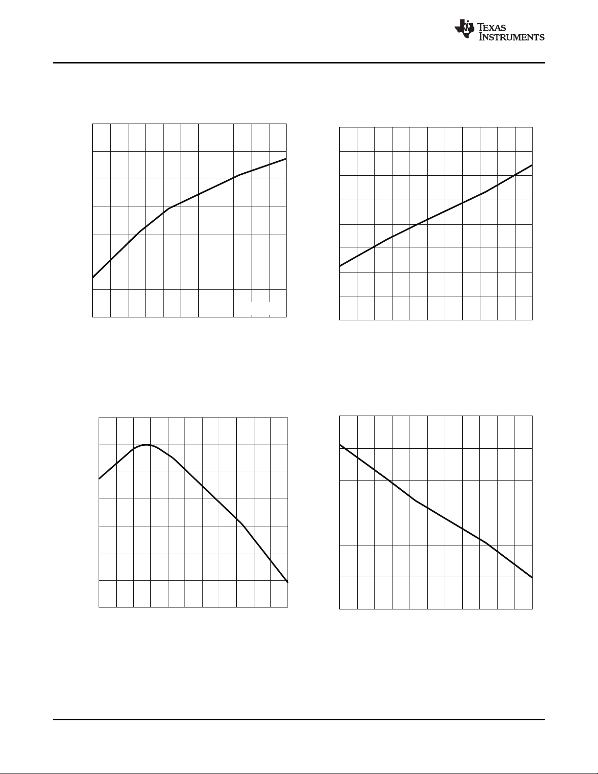
TYPICAL CHARACTERISTICS (continued)
SHUTDOWN CURRENT OCSET CURRENT SOURCE
vs vs
JUNCTION TEMPERATURE JUNCTION TEMPERATURE
www.ti.com
6 Submit Documentation Feedback Copyright © 2009, Texas Instruments Incorporated
Figure 5. Figure 6.
FEEDBACK REFERENCE VOLTAGE ENABLE HIGH-LEVEL THRESHOLD VOLTAGE
vs vs
JUNCTION TEMPERATURE JUNCTION TEMPERATURE
Figure 7. Figure 8.
Product Folder Link(s) :TPS40303 TPS40304 TPS40305
TJ– Junction Temperature – °C
V
OCH
– High-Side Overcurrent Threshold – mV
–40 20–25 –10 5 65 12580 95 11035 50
350
400
450
500
550
600
–40 20–25 –10 5 65 12580 95 11035 50
TJ– Junction Temperature – °C
300.0
300.5
301.0
301.5
302.0
302.5
303.0
V
IL
– Enable Low-Level Threshold Voltage – mV
–40 20–25 –10 5 65 12580 95 11035 50
TJ– Junction Temperature – °C
V
OV
/V
UV
– Power Good Threshold Voltage – mV
400
450
500
550
600
650
700
750
800
Undervoltage
Overvoltage
750
775
800
825
850
875
900
925
950
975
1000
–40 20–25 –10 5 65 12580 95 11035 50
TJ– Junction Temperature – °C
V
SS
– Soft-Start Voltage – mV
www.ti.com
TPS40303, TPS40304, TPS40305
SLUS964 –NOVEMBER 2009
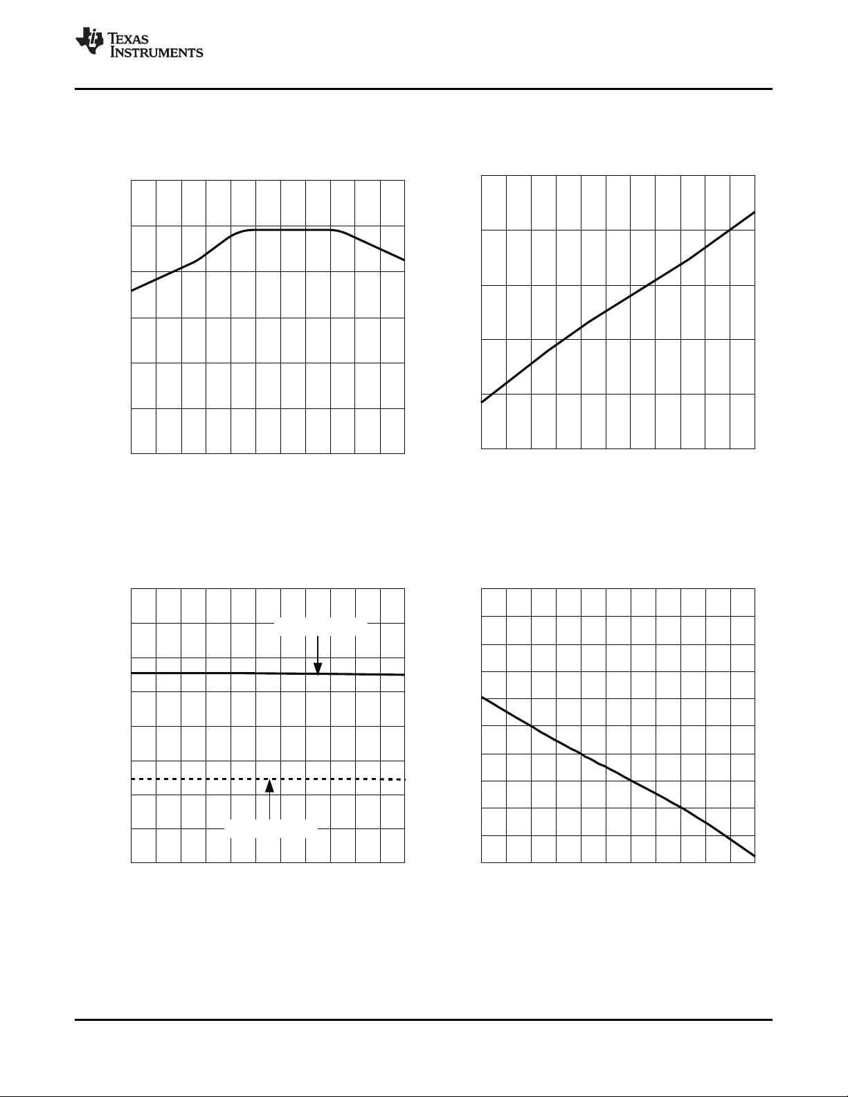
TYPICAL CHARACTERISTICS (continued)
ENABLE LOW-LEVEL THRESHOLD VOLTAGE HIGH-SIDE OVERCURRENT THRESHOLD
vs vs
JUNCTION TEMPERATURE JUNCTION TEMPERATURE
Copyright © 2009, Texas Instruments Incorporated Submit Documentation Feedback 7
Figure 9. Figure 10.
POWER GOOD THRESHOLD VOLTAGE SOFT-START VOLTAGE
vs vs
JUNCTION TEMPERATURE JUNCTION TEMPERATURE
Figure 11. Figure 12.
Product Folder Link(s) :TPS40303 TPS40304 TPS40305
5 4 3 2 1
6 7 8 9 10
FB COMP PGOOD EN/SS VDD
BOOT HDRV SW
LDRV/
OC
BP
Thermal Pad
TPS40303, TPS40304, TPS40305
SLUS964 –NOVEMBER 2009
DEVICE INFORMATION
TERMINAL CONFIGURATION
The package is an 10-Pin SON (DRC) package. Note: The thermal pad is an electrical ground connection.
www.ti.com
TERMINAL
NAME NO.
BOOT 6 I between this pin and SW. For low input voltage operation, an external schottky diode from BP to BOOT is
BP 10 O
COMP 4 O Output of the error amplifier and connection node for loop feedback components.
EN/SS 2 I
FB 5 I
PGOOD 3 O Open drain power good output.
HDRV 7 O Bootstrapped gate drive output for the high side N-channel MOSFET.
LDRV/OC 9 O is also used to determine the voltage level for OCP. An internal current source of 10 µA flows through the
VDD 1 I
SW 8 O
GND
Thermal connection serves a twofold purpose. The first is to provide an electrical ground connection for the device.
Pad The second is to provide a low thermal impedance path from the device die to the PCB. This pad should be
PIN FUNCTIONS
I/O DESCRIPTION
Gate drive voltage for the high side N-channel MOSFET. A 100 nF capacitor (typical) must be connected
recommended to maximize the gate drive voltage for the high-side.
Output bypass for the internal regulator. Connect a low ESR bypass ceramic capacitor of 1 µF or greater from
this pin to GND.
Logic level input which starts or stops the controller via an external user command. Letting this pin float turns
the controller on. Pulling this pin low disables the controller. This is also the soft-start programming pin. A
capacitor connected from this pin to GND programs the soft-start time. The capacitor is charged with an
internal current source of 10 µA. The resulting voltage ramp of this pin is also used as a second non-inverting
input to the error amplifier after a 0.8 V (typical) level shift downwards. Output regulation is controlled by the
internal level shifted voltage ramp until that voltage reaches the internal reference voltage of 600 mV – the
voltage ramp of this pin reaches 1.4 V (typical). Optionally, a 267 kΩ resistor from this pin to BP enables
frequency spread spectrum feature.
Inverting input to the error amplifier. In normal operation, the voltage on this pin is equal to the internal
reference voltage.
Gate drive output for the low side synchronous rectifier N-channel MOSFET. A resistor from this pin to GND
resistor during initial calibration and that sets up the voltage trip point used for OCP.
Power input to the controller. Bypass VDD to GND with a low ESR ceramic capacitor of at least 1.0-µF close
to the device.
Sense line for the adaptive anti-cross conduction circuitry. Serves as common connection for the flying high
side FET driver.
Ground connection to the controller. This is also the thermal pad used to conduct heat from the device. This
tied externally to a ground plane.
8 Submit Documentation Feedback Copyright © 2009, Texas Instruments Incorporated
Product Folder Link(s) :TPS40303 TPS40304 TPS40305
BOOT
SW
LDRV/OC
EN/SS
COMP
FB
GND
VDD
BP
PGOOD
2
1
10
4
5
3
6
7
8
9
PAD
HDRV
+
+
FB
0.6 V
REF
+ 12.5%
0.6 V
REF
–12.5%
+
Fault
Controller
SS
Soft Start
BP
Anti-Cross
Conduction
and
Pre-Bias
Circuit
PWM
Logic
BP
Clock
6-V
Regulator
References
0.6 V
REF
SD
BP
Spread
Spectrum
Oscillator
+
Calibration
Circuit
+
UDG-09160
0.6 V
REF
SS
10 mA
750 kW
Fault Controller
Thermal
Shutdown
OC
Threshold
Setting
10 mA
OC
SS
SD
PWM
Clock
OC
www.ti.com
TPS4030x BLOCK DIAGRAM
TPS40303, TPS40304, TPS40305
SLUS964 –NOVEMBER 2009
Copyright © 2009, Texas Instruments Incorporated Submit Documentation Feedback 9
Product Folder Link(s) :TPS40303 TPS40304 TPS40305
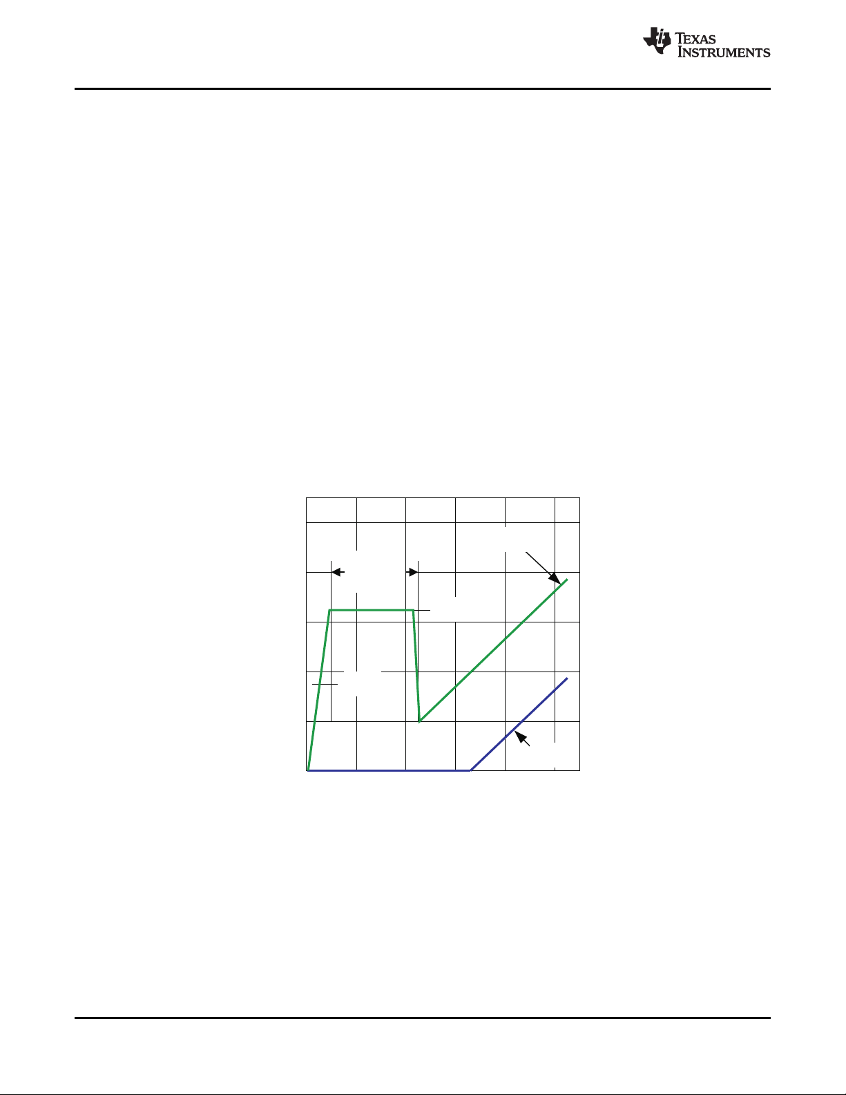
0
0.4
0.7 V
0.8
1.3 V
1.2
1.6
2.0
V
EN/SS
t – Time – ms
Calibration
Time
1.9 ms
V
IN
– Input Voltage – V
V
SS_INT
UDG-09159
TPS40303, TPS40304, TPS40305
SLUS964 –NOVEMBER 2009
APPLICATION INFORMATION
Introduction
The TPS4030x is a family of cost-optimized synchronous buck controllers providing high-end features to
construct high-performance DC/DC converters. Pre-bias capability eliminates concerns about damaging sensitive
loads during startup. Programmable over-current protection levels and hiccup over-current fault recovery
maximize design flexibility and minimize power dissipation in the event of a prolonged output short. Frequency
Spread Spectrum (FSS) feature reduces peak EMI noise by spreading the initial energy of each harmonic along
a frequency band, thus giving a wider spectrum with lower amplitudes.
Voltage Reference
The 600 mV band gap cell is internally connected to the non-inverting input of the error amplifier. The reference
voltage is trimmed with the error amplifier in a unity gain configuration to remove amplifier offset from the final
regulation voltage. The 1% tolerance on the reference voltage allows the user to design a very accurate power
supply.
Enable Functionality, Startup Sequence and Timing
After input power is applied, an internal current source of 40 µA starts to charge up the soft-start capacitor
connected from EN/SS to GND. When the voltage across that capacitor increases to 0.7 V, it enables the internal
BP regulator followed by a calibration. The total calibration time is about 1.9 ms. See Figure 13. During the
calibration, the device performs in the following way. It disables the LDRV drive and injects an internal 10 µA
current source to the resistor connected from LDRV to GND. The voltage developed across that resistor is then
sampled and latched internally as the OCP trip level until one cycles the input or toggles the EN/SS.
www.ti.com
The voltage at EN/SS is internally clamped to 1.3 V before and/or during calibration to minimize the discharging
time once calibration is complete. The discharging current is from an internal current source of 140 µA and it
pulls the voltage down to 0.4 V. It then initiates the soft-start by charging up the capacitor using an internal
current source of 10 µA. The resulting voltage ramp on this pin is used as a second non-inverting input to the
error amplifier after an 800 mV (typical) downward level-shift; therefore, actual soft-start will not take place until
the voltage at this pin reaches 800 mV.
Figure 13. Startup Sequence and Timing
If EN/SS is left floating, the controller starts automatically. EN/SS must be pulled down to less than 270 mV to
guarantee that the chip is in shutdown mode.
10 Submit Documentation Feedback Copyright © 2009, Texas Instruments Incorporated
Product Folder Link(s) :TPS40303 TPS40304 TPS40305

SS
SS SS
FB
I
C t
V
æ ö
= ´
ç ÷
è ø
TPS40303, TPS40304, TPS40305
www.ti.com
Soft-Start Time
The soft-start time of the TPS4030x is user programmable by selecting a single capacitor. The EN/SS pin
sources 10 µA to charge this capacitor. The actual output ramp-up time is the amount of time that it takes for the
10 µA to charge the capacitor through a 600mV range. There is some initial lag due to calibration and an offset
(800 mV) from the actual EN/SS pin voltage to the voltage applied to the error amplifier.
The soft-start is done in a closed loop fashion, meaning that the error amplifier controls the output voltage at all
times during the soft start period and the feedback loop is never open as occurs in duty cycle limit soft-start
schemes. The error amplifier has two non-inverting inputs, one connected to the 600 mV reference voltage, and
the other connected to the offset EN/SS pin voltage. The lower of these two voltages is what the error amplifier
controls the FB pin to. As the voltage on the EN/SS pin ramps up past approximately 1.4 V (800 mV offset
voltage plus the 600 mV reference voltage), the 600 mV reference voltage becomes the dominant input and the
converter has reached its final regulation voltage.
The capacitor required for a given soft-start ramp time for the output voltage is given by Equation 1.
where
• CSSis the required capacitance on the EN/SS pin (F)
• ISSis the soft-start source current (10 µA)
• VFBis the feedback reference voltage (0.6 V)
• tSSis the desired soft-start ramp time (s)
SLUS964 –NOVEMBER 2009
(1)
Oscillator and Frequency Spread Spectrum (FSS)
The oscillator frequency is internally fixed. The TPS40303 operating frequency is 300 KHz, the TPS40304
operating frequency is 600 KHz and the TPS40305 operating frequency is 1.2 MHz.
Connecting a resistor with a value of 267 kΩ ± 10% from BP to EN/SS enables the FSS feature. When enabled,
it spreads the internal oscillator frequency over a minimum 12% window using a 25-kHz modulation frequency
with triangular profile. By modulating the switching frequency, side-bands are created. The emission power of the
fundamental switching frequency and its harmonics is distributed into smaller pieces scattered around many
side-band frequencies. The effect significantly reduces the peak EMI noise and makes it much easier for the
resultant emission spectrum to pass EMI regulations.
Overcurrent Protection
Programmable OCP level at LDRV is from 6 mV to 150 mV at room temperature with 3000 ppm temperature
coefficient to help compensate for changes in the low side FET channel resistance as temperature increases.
With a scale factor of 2, the actual trip point across the low side FET is in the range of 12 mV to 300 mV. The
accuracy of the internal current source is ±5%. Overall offset voltage, including the offset voltage of the internal
comparator and the amplifier for scale factor of 2, is limited to ±8 mV.
Maximum clamp voltage at LDRV is 340 mV to avoid turning on the low side FET during calibration and in a
pre-biased condition. The maximum clamp voltage is fixed and it does not change with temperature. If the
voltage drop across R
included), it disables OC protection. Once disabled, there is no low side or high side current sensing.
OCP level at HDRV is fixed at 450 mV with 3000 ppm temperature coefficient to help compensate for changes in
the high side FET channel resistance as temperature increases. OCP at HDRV provides pulse-by-pulse current
limiting.
reaches the 340 mV maximum clamp voltage during calibration (No R
OCSET
OCSET
resistor
Copyright © 2009, Texas Instruments Incorporated Submit Documentation Feedback 11
Product Folder Link(s) :TPS40303 TPS40304 TPS40305

( ) ( )
P P
OCLOS
OUT m ax DS on
OCSET
OCSET
I
I R V
2
R
2 I
-
æ ö
æ ö
æ ö
- ´ -
ç ÷
ç ÷
ç ÷
è ø
ç ÷
è ø
=
ç ÷
´
ç ÷
ç ÷
è ø
TPS40303, TPS40304, TPS40305
SLUS964 –NOVEMBER 2009
OCP sensing at LDRV is a true inductor valley current detection, using sample and hold. Equation 2 can be used
to calculate R
OCSET
:
where
• I
• V
• I
• R
• I
• R
To avoid over-current tripping in normal operating load range, calculate R
• The maximum R
• The lower limit of V
is the internal current source
OCSET
is the overall offset voltage
OCLOS
is the peak-to-peak inductor current
P-P
is the drain to source on-resistance of the low-side FET
DS(on)
OUT(max)
is the trip point for OCP
is the resistor used for setting the OCP level
OCSET
at room temperature
DS(ON)
(–8 mV) and the lower limit of I
OCLOS
using the equation above with:
OCSET
(9.5 µA) from the Electrical Characteristics
OCSET
table.
• The peak-to-peak inductor current I
at minimum input voltage
P-P
Overcurrent is sensed across both the low-side FET and the high-side FET. If the voltage drop across either FET
exceeds the OC threshold, a count increments one count. If no OC is detected on either FET, the fault counter
decrements by one count. If three OC pulses are summed, a fault condition is declared which cycles the
soft-start function in a hiccup mode. Hiccup mode consists of four dummy soft-start timeouts followed by a real
one if overcurrent condition is encountered during normal operation, or five dummy soft-start timeouts followed
by a real one if overcurrent condition occurs from the beginning during start. This cycle continues indefinitely until
the fault condition is removed.
www.ti.com
(2)
Drivers
The drivers for the external high-side and low-side MOSFETs are capable of driving a gate-to-source voltage of
VBP. The LDRV driver for the low-side MOSFET switches between BP and GND, while HDRV driver for the
high-side MOSFET is referenced to SW and switches between BOOT and SW. The drivers have
non-overlapping timing that is governed by an adaptive delay circuit to minimize body diode conduction in the
synchronous rectifier.
Pre-Bias Startup
The TPS4030x contains a circuit to prevent current from being pulled from the output during startup in the
condition the output is pre-biased. There are no PWM pulses until the internal soft-start voltage rises above the
error amplifier input (FB pin), if the output is pre-biased. Once the soft-start voltage exceeds the error amplifier
input, the controller slowly initiates synchronous rectification by starting the synchronous rectifier with a narrow
on time. It then increments that on time on a cycle-by-cycle basis until it coincides with the time dictated by (1-D),
where D is the duty cycle of the converter. This approach prevents the sinking of current from a pre-biased
output, and ensures the output voltage startup and ramp to regulation is smooth and controlled.
12 Submit Documentation Feedback Copyright © 2009, Texas Instruments Incorporated
Product Folder Link(s) :TPS40303 TPS40304 TPS40305

TPS40303, TPS40304, TPS40305
www.ti.com
Power Good
The TPS4030x provides an indication that output is good for the converter. This is an open drain signal and pulls
low when any condition exists that would indicate that the output of the supply might be out of regulation. These
conditions include the following:
• VFBis more than ±12.5% from nominal
• Soft-start is active
• A short circuit condition has been detected
NOTE
When there is no power to the device, PGOOD is not able to pull close to GND if an
auxiliary supply is used for the power good indication. In this case, a built in resistor
connected from drain to gate on the PGOOD pull down device makes the PGOOD pin
look approximately like a diode to GND.
Thermal Shutdown
If the junction temperature of the device reaches the thermal shutdown limit of 145°C, the PWM and the oscillator
are turned off and HDRV and LDRV are driven low. When the junction cools to the required level (125°C typical),
the PWM initiates soft start as during a normal power-up cycle.
SLUS964 –NOVEMBER 2009
Copyright © 2009, Texas Instruments Incorporated Submit Documentation Feedback 13
Product Folder Link(s) :TPS40303 TPS40304 TPS40305

+
TPS40303, TPS40304, TPS40305
SLUS964 –NOVEMBER 2009
DESIGN EXAMPLES
Design Example 1: Using the TPS40305 for a 12 V to 1.8 V Point-of-Load Synchronous Buck Regulator
12 V to 1.8 V Point-of-Load Synchronous Buck Regulator
The following example illustrates the design process and component selection for a 12 V to 1.8 V point-of-load
synchronous buck regulator using the TPS40305.
Table 1. Design Example Electrical Characteristics
PARAMETER TEST CONDITIONS MIN TYP MAX UNIT
V
IN
V
IN(ripple)
V
OUT
V
RIPPLE
V
OVER
V
UNDER
I
OUT
t
SS
I
SCP
f
SW
η Efficiency VIN= 12 V, I
η Full load efficiency VIN= Nom, I
Input voltage 8 14 V
Input ripple voltage I
Output voltage 0 A ≤ I
= 10 A 0.6 V
OUT
≤ 10 A 1.764 1.800 1.836 V
OUT
Line regulation 8 V ≤ VIN≤ 14 V 0.5%
Load regulation 0 A ≤ I
Output voltage ripple I
Output overshoot I
Output undershoot I
OUT
OUT
OUT
≤ 10 A 0.5%
OUT
= 10 A 36 mV
falling from 7 A to 3 A 100 mV
rising from 3 A to 7 A 100 mV
Output current 4.5 V ≤ VIN≤ 5.5 V 0 10 A
Soft start time VIN= 12 V 1.5 ms
Short circuit current trip point 13 15 A
Switching frequency 1200 kHz
= 5 A 90%
OUT
= Max 80%
OUT
www.ti.com
Figure 14. TPS40305 Design Example Schematic
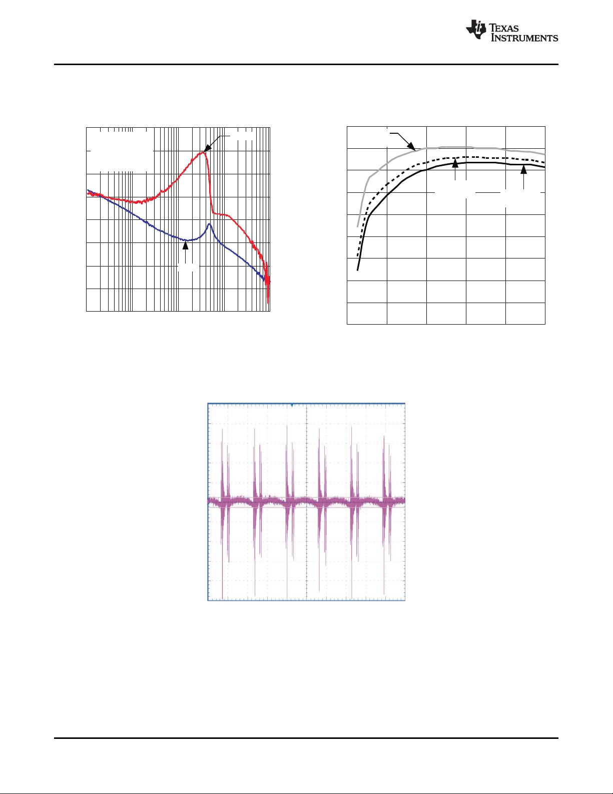
The list of materials for this application is shown in Table 3. The loop response and efficiency from boards built
using this design are shown in Figure 15 and Figure 16. Gerber Files and additional application information are
available from the factory.
Design Procedure
Selecting the Switching Frequency
To achieve the small size for this design the TPS40305, with fSW= 1200 kHz, is selected for minimal external
component size.
14 Submit Documentation Feedback Copyright © 2009, Texas Instruments Incorporated
Product Folder Link(s) :TPS40303 TPS40304 TPS40305

( )
( )
OU T
IN m a x
OU T
OU T SW
IN m a x
V V
V
1 14 V 1.8 V 1.8 V 1
L 47 1nH
0.3 I V f 0.3 1 0 A 14 V 1200 kH z
-
-
» ´ ´ = ´ ´ =
´ ´
( ) ( )
2 2 2 2 2 2
1 1 1
RIPPLE OUT RIPPLE
L rms L avg
12 12 12
I I I I I 10 3.5 10.05 A= + = + = + =
2
TRAN TRAN TRAN TRAN
OVER
OUT OUT OUT OUT OUT
I I I L I L
V T
C C V V C
´ ´
< ´ D = ´ =
´
( )
2
TRAN TRAN TRAN TRAN
UNDER
OUT OUT IN OUT
IN OUT OUT
I I I L I L
V T
C C V V
V V C
´ ´
< ´ D = ´ =
-
- ´
( )
2
2
TRAN(max)
OUT(min)
OUT OVER
I L
4 400nH
C 35 F
1.8 100mV
V V
´
´
= = = m
´
´
RIPPLE
RIPPLE(total)
RIPPLE(total) RIPPLE(cap )
OUT SW
MAX
RIPPLE RIPPLE
I
V
V V
8 C f
ESR
I I
3.5 A
36mV
8 35 F 1200kHz
7m
3.5 A
æ ö
-
ç ÷
-
´ ´
è ø
= =
æ ö
-
ç ÷
´ m ´
è ø
= = W
TPS40303, TPS40304, TPS40305
www.ti.com
Inductor Selection (L1)
Synchronous buck power inductors are typically sized for approximately 30% peak-to-peak ripple current (I
Given this target ripple current, the required inductor size can be calculated in Equation 3.
Selecting a standard 400-nH inductor value, solve for I
RIPPLE
=3.5 A
The RMS current through the inductor is approximated by Equation 4.
Output Capacitor Selection (C12)
The selection of the output capacitor is typically driven by the output transient response. Equation 5 and
Equation 6 overestimate the voltage deviation to account for delays in the loop bandwidth and can be used to
determine the required output capacitance.
SLUS964 –NOVEMBER 2009
RIPPLE
(3)
(4)
(5)
)
(6)
If V
IN(min)
> 2 x V
, use overshoot (Equation 5) to calculate minimum output capacitance. If V
OUT
IN(min)
< 2 x V
OUT
use undershoot(Equation 6) to calculate minimum output capacitance.
(7)
With a minimum capacitance, the maximum allowable ESR is determined by the maximum ripple voltage and is
approximated by Equation 8.
(8)
Two 0805, 22-µF, 6.3 V, X5R ceramic capacitors are selected to provide more than 35-µF of minimum
capacitance and less than 7 mΩ of ESR (2.5 mΩ each).
,
Copyright © 2009, Texas Instruments Incorporated Submit Documentation Feedback 15
Product Folder Link(s) :TPS40303 TPS40304 TPS40305
OUT OUT
CHARGE
SS
V C
1.8 V 2 22 F
I 0.053 A
t 1.5ms
´
´ ´ m
= = =
( )
1 1
OUT(max) RIPPLE CHARGE
L peak
2 2
I I I I 10 A 3.5 A 0.053 A 11.8 A= + + = + ´ + =
LOAD OUT
IN(min)
RIPPLE(cap) IN SW
I V
10 1.8 V
C 12.5 F
V V f 150mV 8 V 1200kHz
´
´
= = = m
´ ´ ´ ´
RIP PLE (esr )
MA X
1
LO AD RIPP LE
2
V
150 mV
ES R 12.7 m
I I 1 1.75 A
= = = W
+
( )
( )
LO AD RMS
RMS c in
I I D 1 D 1 0 A 0.2 2 5 (1 0.2 2 5 ) 4 .17 A = ´ ´ - = ´ ´ - =
= ´ = ´ =
BOOST G2
C 20 Q 20 5nC 100 nF
TPS40303, TPS40304, TPS40305
SLUS964 –NOVEMBER 2009
Peak Current Rating of Inductor
With output capacitance, it is possible to calculate the charge current during start-up and determine the minimum
saturation current rating for the inductor. The start-up charging current is approximated by Equation 9.
Table 2. Inductor Requirements
SYMBOL PARAMETER VALUE UNITS
L Inductance 400 nH
I
L(rms)
I
L(peak)
RMS current (thermal rating) 10.05 A
Peak current (saturation rating) 11.8 A
A PG0083.401, 400 nH inductor is selected for its small size, low DCR (3.0mΩ) and high-current handling
capability (17-A thermal, 27-A saturation).
Input Capacitor Selection (C8)
The input voltage ripple is divided between capacitance and ESR. For this design V
V
RIPPLE(esr)
= 150 mV. The minimum capacitance and maximum ESR are estimated by Equation 11.
RIPPLE(cap)
www.ti.com
(9)
(10)
= 150 mV and
(11)
(12)
The RMS current in the input capacitors is estimated by Equation 13.
(13)
Two 1210, 10-µF, 25-V, X5R ceramic capacitors with approximately 2-mΩ of ESR and a 2.5-A RMS current
rating each are selected. Higher voltage capacitors are selected to minimize capacitance loss at the DC bias
voltage to ensure the capacitors allow sufficient capacitance at the working voltage.
MOSFET Switch Selection (Q1 and Q2)
Reviewing available TI NexFET MOSFETs using TI’s NexFET MOSFET selection tool, the CSD16410Q5A and
CSD16322Q5 5 mm × 6 mm MOSFETs are selected.
These two FETs have maximum total gate charges of 5 nC and 10 nC respectively, which draws 18 mA at 1.2
MHz from the BP regulator, less than its 50 mA minimum rating.
Bootstrap Capacitor (C6)
To ensure proper charging of the high-side FET gate, limit the ripple voltage on the boost capacitor to less than
50 mV.
(14)
VDD Bypass Capacitor (C7)
Per the TPS40305 Electrical Characteristics specifications, select a 1.0-µF X5R or better ceramic bypass
capacitor for VDD.
BP Bypass Capacitor (C5)
As listed in the Electrical Characteristics table, a minimum of 1.0-µF ceramic capacitance is required to stabilize
the BP regulator. To limit regulator noise to less than 10 mV, the value of the bypass capacitor is calculated in
Equation 15.
16 Submit Documentation Feedback Copyright © 2009, Texas Instruments Incorporated
Product Folder Link(s) :TPS40303 TPS40304 TPS40305

BP G1 G2
C 100 MAX(Q ,Q )= ´
( )
1 1
OC LOAD RIPPLE
DS on Q1
2 2
V (1.3 I I ) 1.2 R (1.3 10 A 3.5 A) 1.2 4.6m 62.1mV= ´ - ´ ´ = ´ - ´ ´ W =
OC OCLOS(min)
CS
OCSET(min)
V V
62.1mV ( 8mV)
R 3.69 k 3.74k
2 I 2 9.5 A
-
- -
= = = W » W
´ ´ m
FB
OUT FB
V R4
0.600 V 10.0 k
R5 5.0k 4.99k
V V 1.8 V 0.600 V
´
´ W
= = = W » W
- -
TPS40303, TPS40304, TPS40305
www.ti.com
Since Q1 is larger than Q2, and the total gate charge of Q1 is 10 nC, a BP capacitor of 1.0 µF is calculated. A
standard value of 1.0 µF is selected to limit noise on the BP regulator.
Short Circuit Protection (R11)
The TPS40305 uses the negative drop across the low-side FET at the end of the OFF time to measure the
inductor current. Allowing for 30% over maximum load and 20% rise in R
DS(on)Q1
for self-heating, the voltage drop
across the low-side FET at current limit is given by Equation 16.
The TPS40305 internal temperature coefficient helps compensate for the MOSFET’s R
coefficient, so the current limit programming resistor is selected by Equation 17.
Feedback Divider (R4, R5)
The TPS40305 controller uses a full operational amplifier with an internally fixed 0.600-V reference. R4 is
selected between 10 kΩand 50 kΩ for a balance of feedback current and noise immunity. With R4 set to 10 kΩ,
The output voltage is programmed with a resistor divider given by Equation 18.
SLUS964 –NOVEMBER 2009
(15)
(16)
temperature
DS(on)
(17)
(18)
Compensation: (C2, C3, C4, R3, R6)
Using the TPS40k Loop Stability Tool for 100 kHz bandwidth and 60° phase margin with a R4 value of 10.0 kΩ,
the following values are returned.
• C2 = C_1 = 820 pF
• C3 = C_3 = 150 pF
• C4 = C_2 = 3300 pF
• R3 = R_2 = 422 Ω
• R6 = R_3 = 2.20 kΩ
Copyright © 2009, Texas Instruments Incorporated Submit Documentation Feedback 17
Product Folder Link(s) :TPS40303 TPS40304 TPS40305
0.1
-20
-60
1
100 1 k10
0
-40
80
40
100
60
20
f – Frequency – kHz
Gain
Phase
Gain – dB
Phase – °
-45
-135
0
-90
180
90
225
135
45
VIN= 14 V
I
OUT
= 10 A
BW = 82 kHz
Phase Margin 55°
0
55
50
2
65
60
85
80
95
90
75
70
104 6 8
VIN= 8 V
I
LOAD
– Load Current – A
h – Efficiency – %
VIN= 12 V
VIN= 14 V
TPS40303, TPS40304, TPS40305
SLUS964 –NOVEMBER 2009
Design Example Typical Performance Characteristics
GAIN AND PHASE EFFICIENCY
vs vs
FREQUENCY LOAD CURRENT
www.ti.com
Figure 15. Figure 16.
..
vs
..
Figure 17. Output Ripple (500 MHz Bandwidth)
18 Submit Documentation Feedback Copyright © 2009, Texas Instruments Incorporated
Product Folder Link(s) :TPS40303 TPS40304 TPS40305

TPS40303, TPS40304, TPS40305
www.ti.com
TPS40305 Design Example List of Materials
Table 3. Design Example List of Materials
REFERENCE
DESIGNATOR
C1 1 3.3 nF Capacitor, Ceramic, 10 V, X7R, 20% 0603 Std Std
C2 1 820 pF Capacitor, Ceramic, 25 V, X7R, 10% 0603 Std Std
C3 1 150 pF Capacitor, Ceramic, 25 V, X7R, 10% 0603 Std Std
C4 1 3300 pF Capacitor, Ceramic, 25 V, X7R, 10% 0603 Std Std
C5 1 1.0 µF Capacitor, Ceramic, 10 V, X7R, 20% 0805 Std Std
C6 1 100 nF Capacitor, Ceramic, 16 V, X7R, 20% 0603 Std Std
C7 1 1 µF Capacitor, Ceramic, 25 V, X7R, 20% 0805 Std Std
C8 2 10 µf Capacitor, Ceramic, 25 V, X7R, 10% 1210 Std Std
C11 1 330 µF Capacitor, Aluminum, 25 V, ±20%, 160mohms EEVFK1E331P Panasonic
C12 2 22 µF Capacitor, Ceramic, 6.3 V, X5R, 20% 0805 Std Std
L1 1 0.32 µH Inductor, SMT, 17 A PG0083.401 Pulse
Q1 1 MOSFET, N-Channel, 25 V, 97 A, 4.6 mΩ CSD16322Q5 TI
Q2 1 MOSFET, N-Channel, 25V, 59 A, 9.6 mΩ CSD16410Q5A TI
R3 1 422 Ω Resistor, Chip, 1/16W, 1% 0603 Std Std
R4 1 10.0 kΩ Resistor, Chip, 1/16W, 1% 0603 Std Std
R5 1 4.99 kΩ Resistor, Chip, 1/16W, 1% 0603 Std Std
R6 1 2.20 kΩ Resistor, Chip, 1/16W, 1% 0603 Std Std
R8 1 100 kΩ Resistor, Chip, 1/16W, 1% 0603 Std Std
R10 1 2 Ω Resistor, Chip, 1/16W, 1% 0603 Std Std
R11 1 3.74 kΩ Resistor, Chip, 1/16W, 1% 0603 Std Std
U1 1 IC, 3V-20V sync. 1.2MHz Buck controller DRC10 TPS40305DRC TI
QTY VALUE DESCRIPTION SIZE PART NUMBER MFR
0.328 x
0.390 inch
0.268 x
0.268 inch
QFN-8
POWER
QFN-8
POWER
SLUS964 –NOVEMBER 2009
Copyright © 2009, Texas Instruments Incorporated Submit Documentation Feedback 19
Product Folder Link(s) :TPS40303 TPS40304 TPS40305
TPS40303, TPS40304, TPS40305
SLUS964 –NOVEMBER 2009
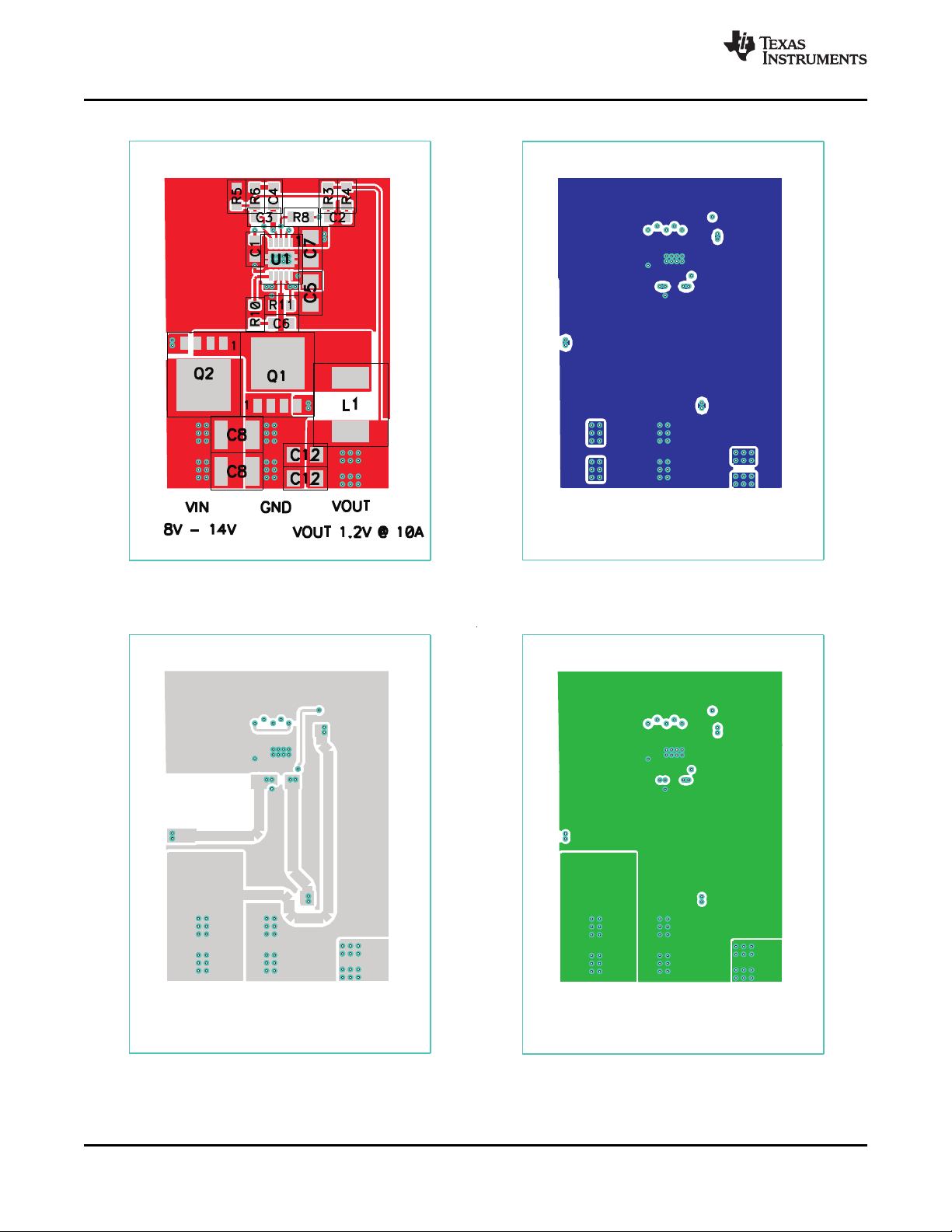
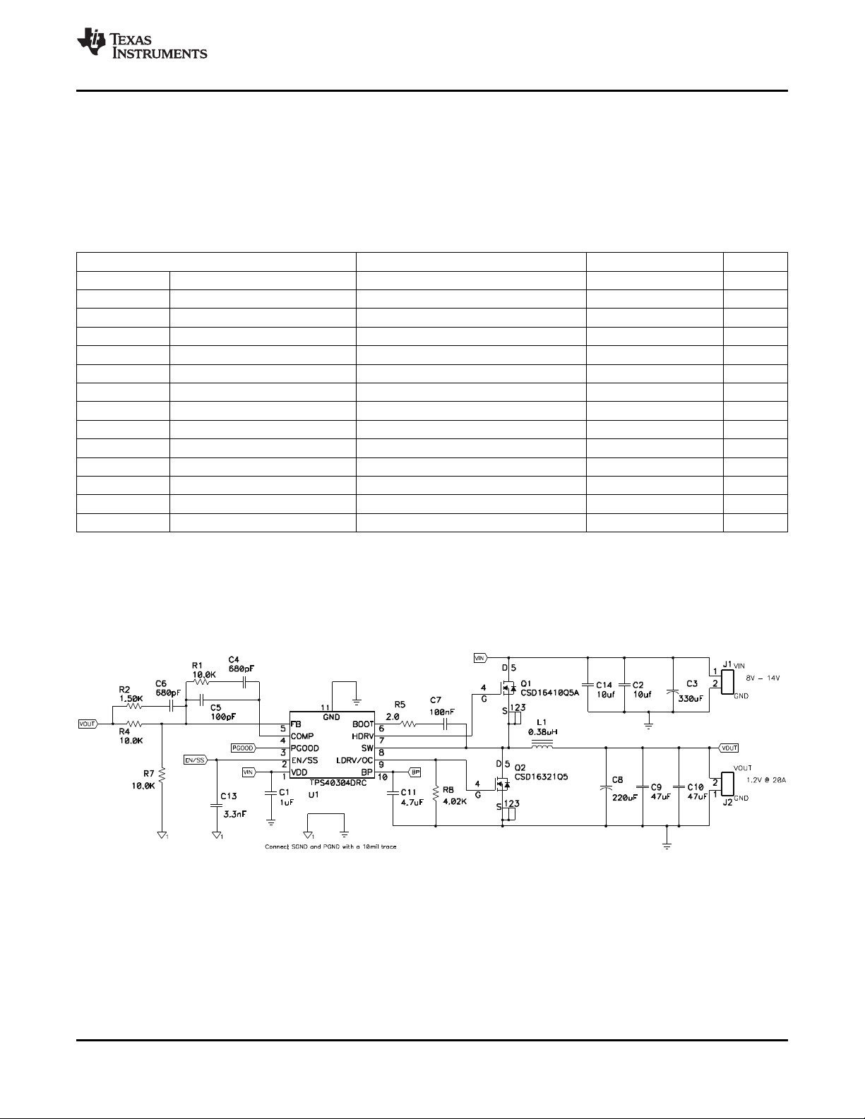
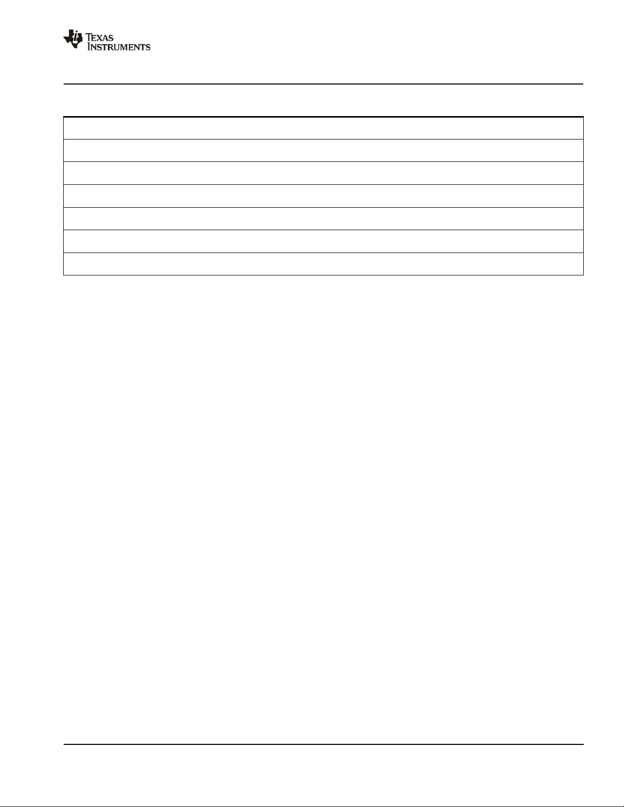
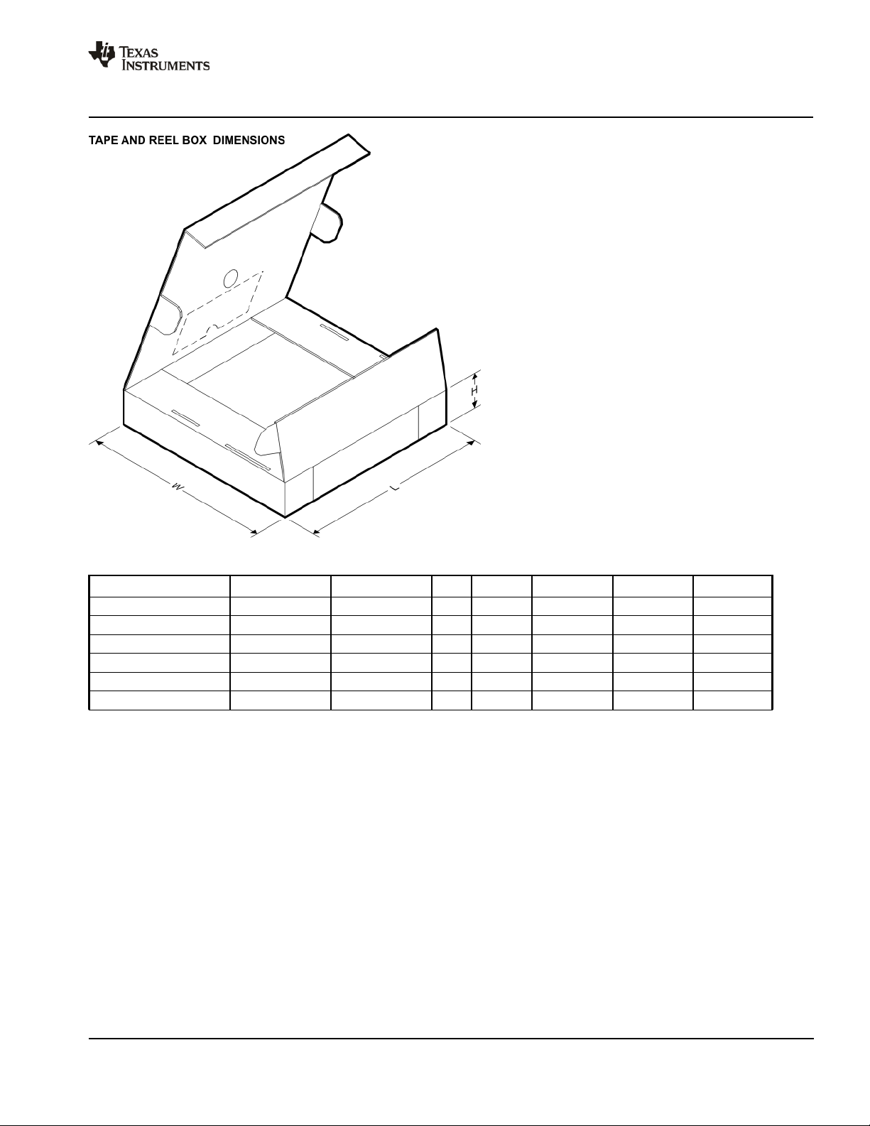
Layout Information
www.ti.com
Figure 18. Top Copper with Components Figure 19. Top Internal Copper Layout
.. ..
.. ..
Figure 20. Bottom Internal Copper Layout Figure 21. Bottom Copper Layer
20 Submit Documentation Feedback Copyright © 2009, Texas Instruments Incorporated
Product Folder Link(s) :TPS40303 TPS40304 TPS40305
+
+
TPS40303, TPS40304, TPS40305
www.ti.com
Design Example 2: A High Current, Low Voltage Design Using the TPS40304
For this 20-A, 12-V to 1.2-V design, the 600kHz, TPS40304 was selected for the balance between small size and
high efficiency.
System Design Specifications
The system design specifications are shown in Table 4.
Table 4. Design Example Electrical Characteristics
PARAMETER TEST CONDITIONS MIN TYP MAX UNIT
V
IN
V
INripple
V
OUT
V
RIPPLE
V
OVER
V
UNDER
I
OUT
t
SS
I
SCP
f
SW
Input voltage 8.0 14 V
Input ripple I
Output voltage 0 A ≤I
= 20 A 0.5 V
OUT
≤ 20 A 1.164 1.200 1.236 V
OUT
Line regulation 8 V ≤ VIN≤14 V 0.5%
Load regulation 0 A ≤I
Output ripple I
OUT
Output overshoot 5 A ≤I
Output undershoot 5 A ≤I
≤ 20 A 0.5%
OUT
= 20 A 36 mV
≤ 15 A 100 mV
OUT
≤ 15 A 100 mV
OUT
Output current 8 V ≤ VIN≤14 V 0 20 A
Soft-start time VIN= 12 V 1.5 ms
Short-circuit current trip point 26 A
Efficiency VIN= 12 V, I
= 12 A %
OUT
Switching frequency 600 kHz
Size 1.5 in
SLUS964 –NOVEMBER 2009
2
Schematic
Figure 22. TPS40304 Design Example Schematic
Copyright © 2009, Texas Instruments Incorporated Submit Documentation Feedback 21
Product Folder Link(s) :TPS40303 TPS40304 TPS40305

1 k
–20
–60
10 k
100 k 1 M
Gain
Phase
0
–40
80
40
100
60
20
Gain – dB
Phase – °
–45
–135
0
–90
180
90
225
135
45
f – Frequency – Hz
60
50
65
55
90
80
95
85
75
h – Efficiency – %
70
0 5 15 20
I
LOAD
– Load Current – A
10
VIN= 14 V
VIN= 8 V
VIN= 12 V
TPS40303, TPS40304, TPS40305
SLUS964 –NOVEMBER 2009
Typical Performance Characteristics
EFFICIENCY GAIN AND PHASE
vs vs
LOAD CURRENT FREQUENCY
www.ti.com
Figure 23. Figure 24.
Figure 25. Output Ripple 10 mV/div, 2-µs/div, 20-MHz Bandwidth
22 Submit Documentation Feedback Copyright © 2009, Texas Instruments Incorporated
Product Folder Link(s) :TPS40303 TPS40304 TPS40305

+ +
TPS40303, TPS40304, TPS40305
www.ti.com
Design Example 3: A Synchronous Buck Application Using the TPS40303
This example illustrates a 3.3-V/5-V/12-V to 0.6-V at 10-A synchronous buck application using the TPS40303
switching at 300 kHz.
Schematic
SLUS964 –NOVEMBER 2009
Figure 26. TPS40303 Design Example Schematic
Typical Performance Characteristics
A typical efficiency graph for this design example using the TPS40303 is shown in Figure 27.The typical line and
load regulation this design example using the TPS40303 is shown in Figure 28
Copyright © 2009, Texas Instruments Incorporated Submit Documentation Feedback 23
Product Folder Link(s) :TPS40303 TPS40304 TPS40305

0
2 4 6 8 10
I
LOAD
– Load Current – A
V
OUT
– Output Voltage – V
593
594
595
596
597
598
599
600
601
VIN= 12 V
VIN= 5 V
VIN= 3.3 V
20
0
30
10
80
60
100
70
50
40
0
2 6
10
I
LOAD
– Load Current – A
4
8
90
h – Efficiency – %
VIN= 3.3 V
VIN= 5 V
VIN= 12 V
TPS40303, TPS40304, TPS40305
SLUS964 –NOVEMBER 2009
EFFICIENCY LINE
vs AND LOAD
LOAD CURRENT REGULATION
www.ti.com
Figure 27. Figure 28.
ADDITIONAL REFERENCES
Related Devices
The devices listed in have characteristics similar to the TPS4030x and may be of interest.
Table 5. Related Devices
DEVICE DESCRIPTION
TPS40192/3 4.5 V to 18 V Input 10-pin Synchronous Buck Controller with Power Good
TPS40195 4.5 V to 20 V Synchronous Buck Controller with Synchronization and Power Good
TPS40190 Low Pin Count Synchronous Buck Controller
References
These references, design tools and links to additional references, including design software, may be found at
http://power.ti.com
1. Additional PowerPAD™ information may be found in Applications Briefs (SLMA002A) and (SLMA004).
2. Under The Hood Of Low Voltage DC/DC Converters – SEM1500 Topic 5 – 2002 Seminar Series
3. Understanding Buck Power Stages in Switchmode Power Supplies, (SLVA057), March 1999
4. Designing Stable Control Loops – SEM 1400 – 2001 Seminar Series
Package Outline and Recommended PCB Footprint
The following pages outline the mechanical dimensions of the 10-pin DRC package and provide
recommendations for PCB layout.
24 Submit Documentation Feedback Copyright © 2009, Texas Instruments Incorporated
Product Folder Link(s) :TPS40303 TPS40304 TPS40305
PACKAGE OPTION ADDENDUM
www.ti.com 11-Dec-2009
PACKAGING INFORMATION
Orderable Device Status
(1)
Package
Type
Package
Drawing
Pins Package
Qty
Eco Plan
TPS40303DRCR ACTIVE SON DRC 10 3000 Green (RoHS &
(2)
Lead/Ball Finish MSL Peak Temp
CU NIPDAU Level-2-260C-1 YEAR
(3)
no Sb/Br)
TPS40303DRCT ACTIVE SON DRC 10 250 Green (RoHS &
CU NIPDAU Level-2-260C-1 YEAR
no Sb/Br)
TPS40304DRCR ACTIVE SON DRC 10 3000 Green (RoHS &
CU NIPDAU Level-2-260C-1 YEAR
no Sb/Br)
TPS40304DRCT ACTIVE SON DRC 10 250 Green (RoHS &
CU NIPDAU Level-2-260C-1 YEAR
no Sb/Br)
TPS40305DRCR ACTIVE SON DRC 10 3000 Green (RoHS &
CU NIPDAU Level-2-260C-1 YEAR
no Sb/Br)
TPS40305DRCT ACTIVE SON DRC 10 250 Green (RoHS &
CU NIPDAU Level-2-260C-1 YEAR
no Sb/Br)
(1)
The marketing status values are defined as follows:
ACTIVE: Product device recommended for new designs.
LIFEBUY: TI has announced that the device will be discontinued, and a lifetime-buy period is in effect.
NRND: Not recommended for new designs. Device is in production to support existing customers, but TI does not recommend using this part in
a new design.
PREVIEW: Device has been announced but is not in production. Samples may or may not be available.
OBSOLETE: TI has discontinued the production of the device.
(2)
Eco Plan - The planned eco-friendly classification: Pb-Free (RoHS), Pb-Free (RoHS Exempt), or Green (RoHS & no Sb/Br) - please check
http://www.ti.com/productcontent for the latest availability information and additional product content details.
TBD: The Pb-Free/Green conversion plan has not been defined.
Pb-Free (RoHS): TI's terms "Lead-Free" or "Pb-Free" mean semiconductor products that are compatible with the current RoHS requirements
for all 6 substances, including the requirement that lead not exceed 0.1% by weight in homogeneous materials. Where designed to be soldered
at high temperatures, TI Pb-Free products are suitable for use in specified lead-free processes.
Pb-Free (RoHS Exempt): This component has a RoHS exemption for either 1) lead-based flip-chip solder bumps used between the die and
package, or 2) lead-based die adhesive used between the die and leadframe. The component is otherwise considered Pb-Free (RoHS
compatible) as defined above.
Green (RoHS & no Sb/Br): TI defines "Green" to mean Pb-Free (RoHS compatible), and free of Bromine (Br) and Antimony (Sb) based flame
retardants (Br or Sb do not exceed 0.1% by weight in homogeneous material)
(3)
MSL, Peak Temp. -- The Moisture Sensitivity Level rating according to the JEDEC industry standard classifications, and peak solder
temperature.
Important Information and Disclaimer:The information provided on this page represents TI's knowledge and belief as of the date that it is
provided. TI bases its knowledge and belief on information provided by third parties, and makes no representation or warranty as to the
accuracy of such information. Efforts are underway to better integrate information from third parties. TI has taken and continues to take
reasonable steps to provide representative and accurate information but may not have conducted destructive testing or chemical analysis on
incoming materials and chemicals. TI and TI suppliers consider certain information to be proprietary, and thus CAS numbers and other limited
information may not be available for release.
In no event shall TI's liability arising out of such information exceed the total purchase price of the TI part(s) at issue in this document sold by TI
to Customer on an annual basis.
Addendum-Page 1

PACKAGE MATERIALS INFORMATION
www.ti.com 20-Jul-2010
TAPE AND REEL INFORMATION
*All dimensions are nominal
Device Package
Type
TPS40303DRCR SON DRC 10 3000 330.0 12.4 3.3 3.3 1.1 8.0 12.0 Q2
TPS40303DRCT SON DRC 10 250 180.0 12.4 3.3 3.3 1.1 8.0 12.0 Q2
TPS40304DRCR SON DRC 10 3000 330.0 12.4 3.3 3.3 1.1 8.0 12.0 Q2
TPS40304DRCT SON DRC 10 250 180.0 12.4 3.3 3.3 1.1 8.0 12.0 Q2
TPS40305DRCR SON DRC 10 3000 330.0 12.4 3.3 3.3 1.1 8.0 12.0 Q2
TPS40305DRCT SON DRC 10 250 180.0 12.4 3.3 3.3 1.1 8.0 12.0 Q2
Package
Drawing
Pins SPQ Reel
Diameter
(mm)
Reel
Width
W1 (mm)
A0
(mm)B0(mm)K0(mm)P1(mm)W(mm)
Pin1
Quadrant
Pack Materials-Page 1
PACKAGE MATERIALS INFORMATION
www.ti.com 20-Jul-2010
*All dimensions are nominal
Device Package Type Package Drawing Pins SPQ Length (mm) Width (mm) Height (mm)
TPS40303DRCR SON DRC 10 3000 346.0 346.0 29.0
TPS40303DRCT SON DRC 10 250 190.5 212.7 31.8
TPS40304DRCR SON DRC 10 3000 346.0 346.0 29.0
TPS40304DRCT SON DRC 10 250 190.5 212.7 31.8
TPS40305DRCR SON DRC 10 3000 346.0 346.0 29.0
TPS40305DRCT SON DRC 10 250 190.5 212.7 31.8
Pack Materials-Page 2


IMPORTANT NOTICE
Texas Instruments Incorporated and its subsidiaries (TI) reserve the right to make corrections, modifications, enhancements, improvements,
and other changes to its products and services at any time and to discontinue any product or service without notice. Customers should
obtain the latest relevant information before placing orders and should verify that such information is current and complete. All products are
sold subject to TI’s terms and conditions of sale supplied at the time of order acknowledgment.
TI warrants performance of its hardware products to the specifications applicable at the time of sale in accordance with TI’s standard
warranty. Testing and other quality control techniques are used to the extent TI deems necessary to support this warranty. Except where
mandated by government requirements, testing of all parameters of each product is not necessarily performed.
TI assumes no liability for applications assistance or customer product design. Customers are responsible for their products and
applications using TI components. To minimize the risks associated with customer products and applications, customers should provide
adequate design and operating safeguards.
TI does not warrant or represent that any license, either express or implied, is granted under any TI patent right, copyright, mask work right,
or other TI intellectual property right relating to any combination, machine, or process in which TI products or services are used. Information
published by TI regarding third-party products or services does not constitute a license from TI to use such products or services or a
warranty or endorsement thereof. Use of such information may require a license from a third party under the patents or other intellectual
property of the third party, or a license from TI under the patents or other intellectual property of TI.
Reproduction of TI information in TI data books or data sheets is permissible only if reproduction is without alteration and is accompanied
by all associated warranties, conditions, limitations, and notices. Reproduction of this information with alteration is an unfair and deceptive
business practice. TI is not responsible or liable for such altered documentation. Information of third parties may be subject to additional
restrictions.
Resale of TI products or services with statements different from or beyond the parameters stated by TI for that product or service voids all
express and any implied warranties for the associated TI product or service and is an unfair and deceptive business practice. TI is not
responsible or liable for any such statements.
TI products are not authorized for use in safety-critical applications (such as life support) where a failure of the TI product would reasonably
be expected to cause severe personal injury or death, unless officers of the parties have executed an agreement specifically governing
such use. Buyers represent that they have all necessary expertise in the safety and regulatory ramifications of their applications, and
acknowledge and agree that they are solely responsible for all legal, regulatory and safety-related requirements concerning their products
and any use of TI products in such safety-critical applications, notwithstanding any applications-related information or support that may be
provided by TI. Further, Buyers must fully indemnify TI and its representatives against any damages arising out of the use of TI products in
such safety-critical applications.
TI products are neither designed nor intended for use in military/aerospace applications or environments unless the TI products are
specifically designated by TI as military-grade or "enhanced plastic." Only products designated by TI as military-grade meet military
specifications. Buyers acknowledge and agree that any such use of TI products which TI has not designated as military-grade is solely at
the Buyer's risk, and that they are solely responsible for compliance with all legal and regulatory requirements in connection with such use.
TI products are neither designed nor intended for use in automotive applications or environments unless the specific TI products are
designated by TI as compliant with ISO/TS 16949 requirements. Buyers acknowledge and agree that, if they use any non-designated
products in automotive applications, TI will not be responsible for any failure to meet such requirements.
Following are URLs where you can obtain information on other Texas Instruments products and application solutions:
Products Applications
Amplifiers amplifier.ti.com Audio www.ti.com/audio
Data Converters dataconverter.ti.com Automotive www.ti.com/automotive
DLP® Products www.dlp.com Communications and www.ti.com/communications
DSP dsp.ti.com Computers and www.ti.com/computers
Clocks and Timers www.ti.com/clocks Consumer Electronics www.ti.com/consumer-apps
Interface interface.ti.com Energy www.ti.com/energy
Logic logic.ti.com Industrial www.ti.com/industrial
Power Mgmt power.ti.com Medical www.ti.com/medical
Microcontrollers microcontroller.ti.com Security www.ti.com/security
RFID www.ti-rfid.com Space, Avionics & www.ti.com/space-avionics-defense
RF/IF and ZigBee® Solutions www.ti.com/lprf Video and Imaging www.ti.com/video
Mailing Address: Texas Instruments, Post Office Box 655303, Dallas, Texas 75265
Copyright © 2010, Texas Instruments Incorporated
Telecom
Peripherals
Defense
Wireless www.ti.com/wireless-apps
 Loading...