

8
SLVS612 − APRIL 2006
FEATURES
Operating Input Voltage 10 V to 40 V
D
D Output Voltage Tracks External Reference
D Programmable Fixed-Frequency Up to
100 kHz to 1 MHz Voltage Mode Controller
D Internal Gate Drive Outputs for High-Side
and Synchronous N-Channel MOSFETs
D Externally Synchronizable
D Programmable Short-Circuit Protection
D Thermal Shutdown
D 16-Pin PowerPADt Package (θ
= 2°C/W)
JC
D Programmable Closed-Loop Soft-Start
APPLICATIONS
DDR Tracking Regulators
D
D Power Modules
D Networking Equipment
D Industrial Servers
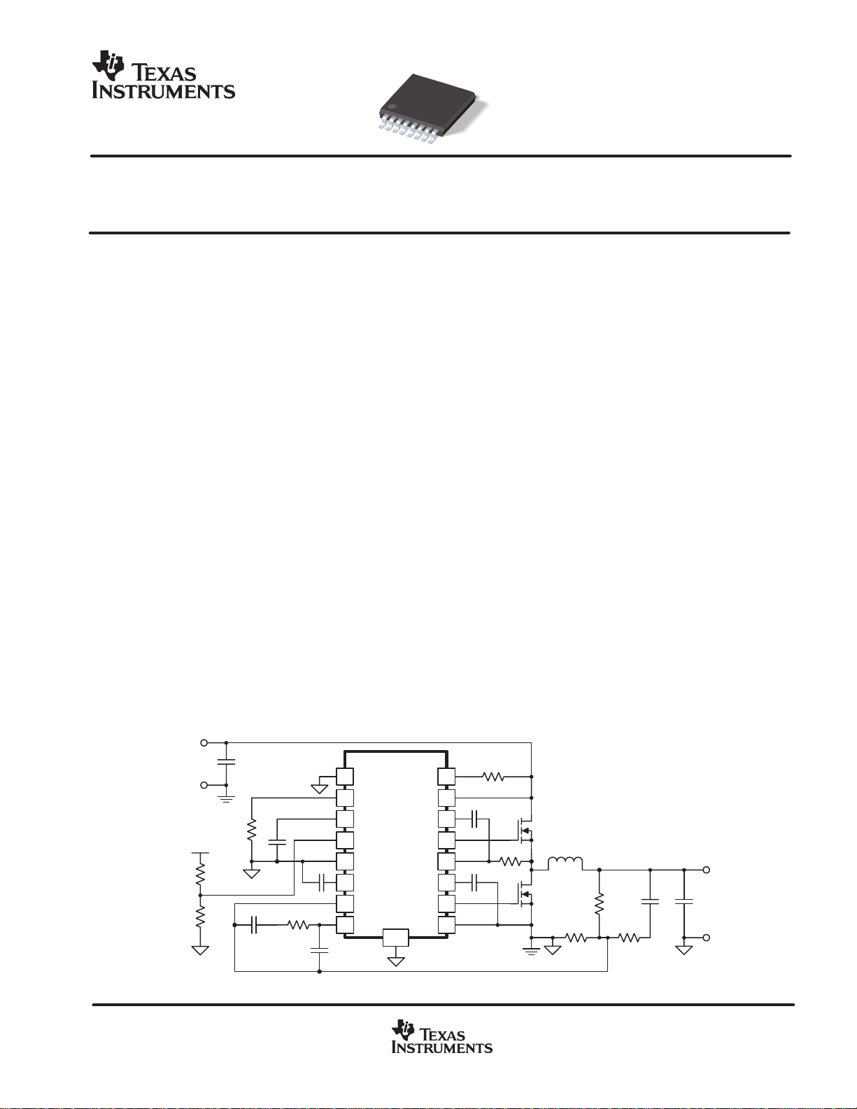
SIMPLIFIED APPLICATION DIAGRAM
CONTENTS
Device Ratings 2
Electrical Characteristics 3
Terminal Information 5
Application Information 7
Design Example 22
Additional References 29
DESCRIPTION
The TPS40056 is part of a family of high-voltage,
wide input, synchronous, step-down converters.
The TPS40056 offers design flexibility with a
variety of user programmable functions, including
soft-start, operating frequency, high-side current
limit, and loop compensation. The TPS40056 is
also synchronizable to an external supply. It
incorporates MOSFET gate drivers for external
N-channel high-side and synchronous rectifier
(SR) MOSFETs. Gate drive logic incorporates
anti-cross conduction circuitry to prevent
simultaneous high-side and synchronous rectifier
conduction. The externally programmable short
circuit protection provides pulse-by-pulse current
limit, as well as hiccup mode operation utilizing an
internal fault counter for longer duration
overloads.
+
V
IN
−
V
TRKIN
!" # $%&" !# '%()$!" *!"&+
*%$"# $ " #'&$$!"# '& ",& "&# &-!# #"%&"#
#"!*!* .!!"/+ *%$" '$&##0 *&# " &$&##!)/ $)%*&
"&#"0 !)) '!!&"&#+
TPS40056PWP
SYNC
1
2
RT
BP5
3
4 EA_REF
5
SGND
6SS
7 VFB
8 COMP
PAD
16
ILIM
15
VIN
14BOOST
HDRV
13
12
SW
BP10
11
LDRV
10
PGND
9
www.ti.com
+
V
TT
−
UDG−03080
Copyright 2006, Texas Instruments Incorporated
1
V
C
SLVS612 − APRIL 2006
These devices have limited built-in ESD protection. The leads should be shorted together or the device placed in conductive foam
during storage or handling to prevent electrostatic damage to the MOS gates.
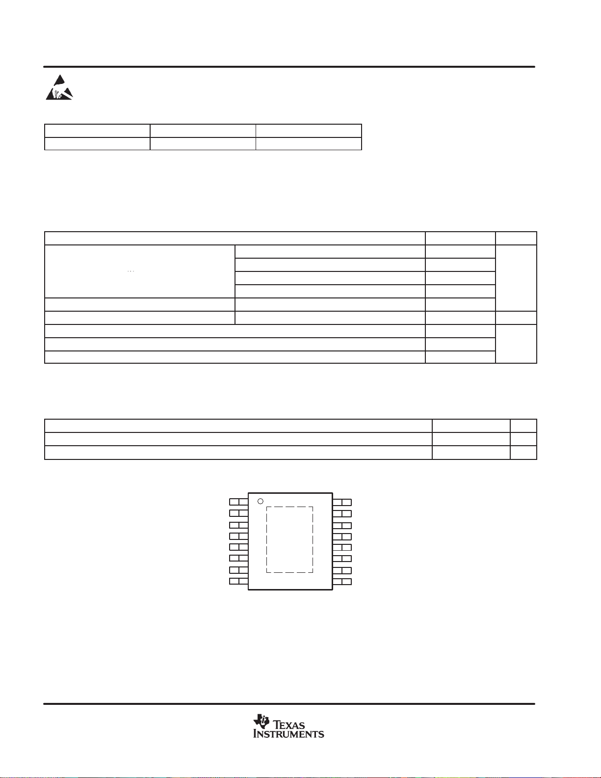
ORDERING INFORMATION
T
A
−40°C to 85°C Plastic HTSSOP(PWP)
(1)
The PWP package is also available taped and reeled. Add an R suffix to the device type
(i.e., TPS40056PWPR). See the application section of the data sheet for PowerPAD
drawing and layout information.
PACKAGE PART NUMBER
(1)
TPS40056PWP
ABSOLUTE MAXIMUM RATINGS
over operating free-air temperature range unless otherwise noted
VIN 45
Input voltage range, V
Output voltage range, V
Output current, I
Operating junction temperature range, T
Storage temperature, T
Lead temperature 1,6 mm (1/16 inch) from case for 10 seconds 260
(2)
Stresses beyond those listed under “absolute maximum ratings” may cause permanent damage to the device. These are stress ratings only ,
and functional operation of the device at these or any other conditions beyond those indicated under “recommended operating conditions” is
not implied. Exposure to absolute-maximum-rated conditions for extended periods may affect device reliability.
IN
O
OUT
J
stg
VFB, SS, SYNC, EA_REF −0.3 to 6
SW −0.3 to 45
SW, transient < 50 ns −2.5
COMP, RT, SS −0.3 to 6
RT 200 µA
(2)
TPS40056 UNIT
−40 to 125
−55 to 150
RECOMMENDED OPERATING CONDITIONS
MIN NOM MAX UNIT
Input voltage, V
Operating free-air temperature, T
I
A
PWP PACKAGE
(TOP VIEW)
(3)(4)
10 40 V
−40 85 °C
V
°C
SYNC
RT
BP5
EA_REF
SGND
SS/SD
VFB
COMP
(3)
For more information on the PWP package, refer to TI Technical Brief, Literature No. SLMA002.
(4)
PowerPADt heat slug must be connected to SGND (pin 5) or electrically isolated from all other pins.
2
1
2
3
THERMAL
4
5
6
7
8
www.ti.com
PAD
16
15
14
13
12
11
10
ILIM
VIN
BOOST
HDRV
SW
BP10
LDRV
9
PGND

ELECTRICAL CHARACTERISTICS
TA = −40°C to 85°C, VIN = 12 Vdc, RT = 90.9 kΩ, fSW = 500 kHz, V
otherwise noted)
PARAMETER
INPUT SUPPLY
V
IN
OPERATING CURRENT
I
DD
BP5
V
BP5
OSCILLATOR/RAMP GENERATOR
f
OSC
V
RAMP
V
IH
V
IL
I
SYNC
V
RT
SOFT START
I
SS
V
SS
t
DSCH
t
SS
BP10
V
BP10
ERROR AMPLIFIER
V
EA_REF
G
BW
G
BW
A
VOL
I
OH
I
OL
V
OH
V
OL
I
BIAS
(1)
(2)
Input voltage range, VIN 10 40 V
Quiescent current
Ouput voltage I
Accuracy 9 V ≤ VIN≤ 40 V 520 580 640 kHz
PWM ramp voltage
High-level input voltage, SYNC 2 5
Low-level input voltage, SYNC 0.8 V
Input current, SYNC 5 10 µA
Pulse width, SYNC 50 ns
RT voltage 2.38 2.50 2.58 V
Maximum duty cycle
Minumum duty cycle VFB ≥ EA_REF + 0.05 V 0%
Soft-start source current 1.65 2.35 3.05 µA
Soft-start clamp voltage 3.7 V
Discharge time CSS = 220 pF 1.6 2.2 2.8
Soft-start time CSS = 220 pF, 0 V ≤ VSS≤ 1.6 V 100 155 205
Ouput voltage 9.0 9.6 10.3 V
Error amplifier reference input voltage
Input offset voltage 0.5 V ≤ VFB≤ 2.25 V −6 6 mV
Input offset voltage 0.2 V ≤ VFB≤ 0.5 V −10 0 10 MV
Gain bandwidth 0.2 V ≤ VFB≤ 0.5 V 1.5 3.5 MHz
Gain bandwidth 0.5 V ≤ VFB≤ 2.25 V 2.5 5.0 MHz
Open loop gain 60 80 dB
High-level output source current 1.5 4.0
Low-level output sink current 2.0 4.0
High-level output voltage I
Low-level output voltage I
Input bias current VFB = 1.2 V 100 200 nA
Ensured by design. Not production tested.
Common mode range extends to ground, but not tested below 200 mV.
(1)
(1)(2)
Output drivers not switching,
VFB = 1.3 V
= 1 mA 4.5 5.0 5.5 V
LOAD
V
PEAK−VVAL
VFB = 0 V, fSW≤ 600 kHz 90%
VFB = 0 V, 600 kHz ≤ fSW≤ 1 MHz
10 V ≤ VIN≤ 40 V 0.2 2.5 V
SOURCE
= 500 µA 0.20 0.35
SINK
SLVS612 − APRIL 2006
EA_REF
= 1.25 V, all parameters at zero power dissipation (unless
TEST CONDITIONS MIN TYP MAX UNIT
1.5 3.0 mA
2.0
85%
mA
= 500 µA 3.2 3.5
V
µs
V
www.ti.com
3
ns
OS
VOSOffset voltage SW vs. ILIM
mV
SLVS612 − APRIL 2006
ELECTRICAL CHARACTERISTICS
TA = −40°C to 85°C, VIN = 12 Vdc, RT = 90.9 kΩ, fSW = 500 kHz, V
otherwise noted)
PARAMETER
CURRENT LIMIT
I
SINK
t
ON
t
OFF
V
OUTPUT DRIVER
t
LRISE
t
LFALL
t
HRISE
t
HFALL
V
V
V
V
SS/SD SHUTDOWN
V
V
BOOST REGULATOR
V
BOOST
SW NODE
I
LEAK
THERMAL SHUTDOWN
T
SD
UVLO
(1)
Current limit sink current 8 10 12 µA
V
= 11.7 V, VSW = (V
Propagation delay to output
Switch leading-edge blanking pulse time
Off time during a fault 7 cycles
Offset voltage SW vs. ILIM
Low-side driver rise time
Low-side driver fall time
High-side driver rise time
High-side driver fall time
High-level ouput voltage, HDRV I
OH
Low-level ouput voltage, HDRV I
OL
High-level ouput voltage, LDRV I
OH
Low-level ouput voltage, LDRV I
OL
Minimum controllable pulse width
Shutdown threshold voltage Outputs off 90 125 165
SD
Device active threshold voltage 165 210 260
EN
Output voltage VIN = 12.0 V 19 20 21 V
Leakage current
Shutdown temperature
Hysteresis
Input voltage UVLO threshold 8.20 8.75 9.25
Input voltage UVLO hysteresis 1.0
Ensured by design. Not production tested.
(1)
(1)
(1)
(1)
(1)
ILIM
V
= 11.7 V, VSW = (V
ILIM
V
= 11.6 V, TA = 25°C −100 −70 −40
ILIM
V
= 11.6 V, 0°C ≤ TA ≤ 85°C
ILIM
V
= 11.6 V, −40°C ≤ TA ≤ 85°C −125 −15
ILIM
C
LOAD
C
LOAD
HDRV =
HDRV =
LDRV =
LDRV =
EA_REF
= 2200 pF
= 2200 pF, (HDRV − SW)
−0.1 A (HDRV − SW)
0.1 A (HDRV − SW) 0.75
−0.1 A
0.1 A 0.5
= 1.25 V all parameters at zero power dissipation (unless
TEST CONDITIONS MIN TYP MAX UNIT
− 0.5 V) 300
ILIM
ILIM
− 2 V)
100
−125 −30
BOOST
−1.5 V
BP10
−1.4 V
250
48 96
24 48
48 96
36 72
BOOST
−1.0 V
BP10
− 1.0 V
100 150 ns
25 µA
165
20
ns
mV
ns
V
mV
°C
V
4
www.ti.com

I/O
DESCRIPTION
SLVS612 − APRIL 2006
TERMINAL FUNCTIONS
TERMINAL
NAME NO.
BOOST 14 O
BP5 3
BP10 11 O
COMP 8 O
HDRV 13 O
ILIM 16 I
EA_REF 4 I Non-inverting input to the error amplifier and used as the reference for the feedback loop.
LDRV 10 O
PGND 9 −
RT 2 I A resistor is connected from this pin to ground to set the internal oscillator and switching frequency.
SGND 5 − Signal ground reference for the device.
SS/SD 6 I
SW 12 I This pin is connected to the switched node of the converter and used for overcurrent sensing.
SYNC 1 I
VFB 7 I
VIN 15 I Supply voltage for the device.
Gate drive voltage for the high side N-channel MOSFET. The BOOST voltage is 9 V greater than the input
voltage. A 0.1-µF ceramic capacitor should be connected from this pin to the SW pin.
5-V reference. This pin should be bypassed to ground with a 0.1-µF ceramic capacitor. This pin may be used
with an external dc load of 1 mA or less.
O
10-V reference used for gate drive of the N-channel synchronous rectifier. This pin should be bypassed by a 1-µF
ceramic capacitor. This pin may be used with an external dc load of 1 mA or less.
Output of the error amplifier , input to the PWM comparator. A feedback network is connected from this pin to the
VFB pin to compensate the overall loop. The comp pin is internally clamped above the peak of the ramp to
improve large signal transient response.
Floating gate drive for the high-side N-channel MOSFET. This pin switches from BOOST (MOSFET on) to SW
(MOSFET off).
Current limit pin, used to set the overcurrent threshold. An internal current sink from this pin to ground sets a
voltage drop across an external resistor connected from this pin to VCC. The voltage on this pin is compared
to the voltage drop (VIN −SW) across the high side MOSFET during conduction.
Gate drive for the N-channel synchronous rectifier. This pin switches from BP10 (MOSFET on) to ground
(MOSFET off).
Power ground reference for the device. There should be a low-impedance path from this pin to the source(s)
of the lower MOSFET(s).
Soft-start programming pin. A capacitor connected from this pin to ground programs the soft-start time. The
capacitor is charged with an internal current source of 2.3 µA. The resulting voltage ramp on the SS pin is used
as a second non-inverting input to the error amplifier. Output voltage regulation is controlled by the SS voltage
ramp until the voltage on the SS pin reaches the internal reference voltage , EA_REF V. Pulling this pin low
disables the controller.
Syncronization input for the device. This pin can be used to synchronize the oscillator to an external master
frequency. If synchronization is not used, connect this pin to SGND.
Inverting input to the error amplifier . In normal operation the voltage on this pin is equal to the EA_REF reference
voltage.
www.ti.com
5
SLVS612 − APRIL 2006
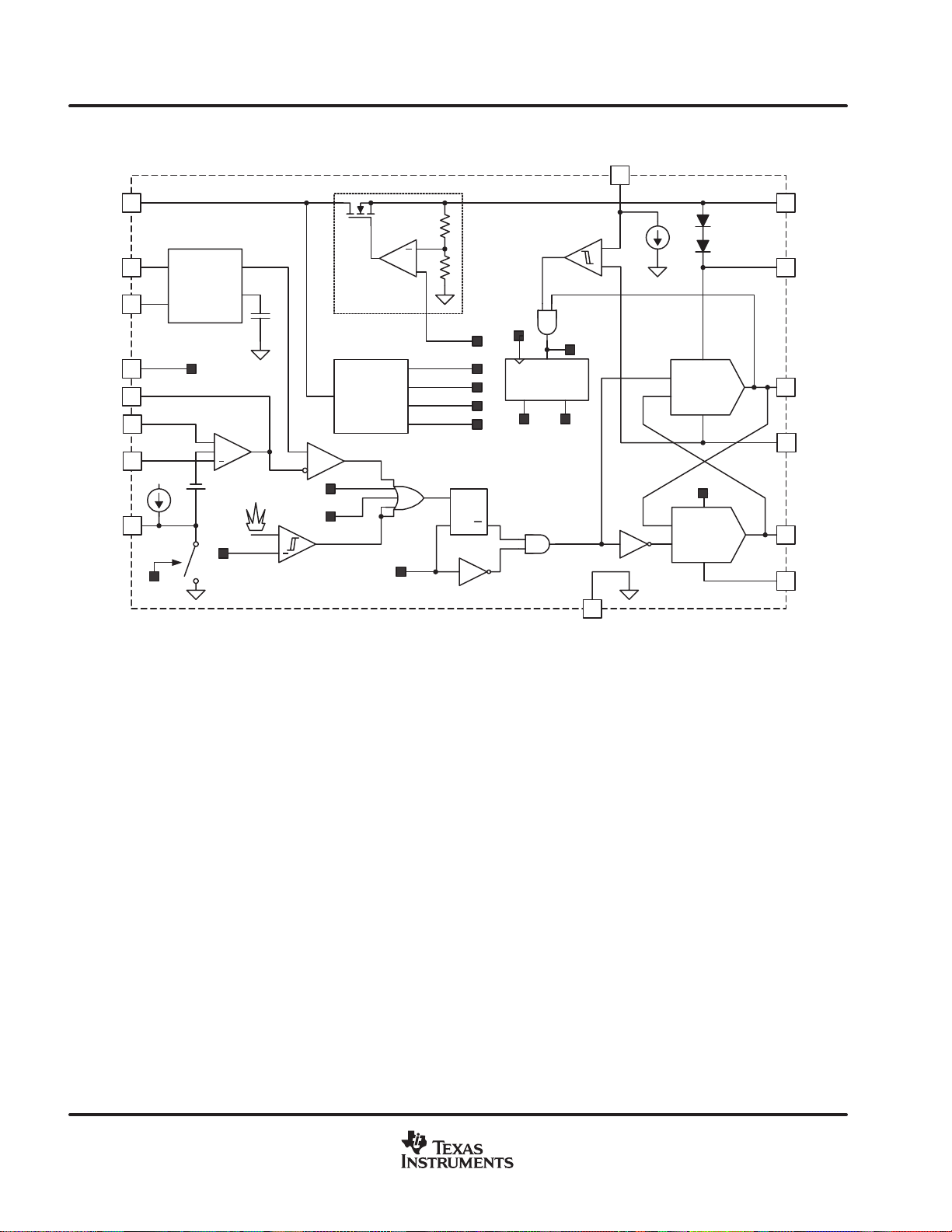
FUNCTIONAL BLOCK DIAGRAM
VIN
ILIM
16
BP10
1115
BP10
RT
SYNC
BP5
COMP
EA_REF
VFB
SS/SD
2
1
BP5
3 7
8
4
7
6
7
Restart
Clock
Oscillator
+
+
0.7 V
+
7
RAMP
0.7 VREF
+
10 V Regulator
7
7
7
7
7
QR
CLK
7
3−Bit Up/Down
Fault Counter
Restart
7
7
7
Fault
CL
5
SGND
N−channel
Driver
BP10
7
N−channel
Driver
1.5 VREF
0.7 VREF
Reference
Voltages
Fault
7
CL
7
+
CLK
1.5 VREF
3.5 VREF
BP5
SQ
7
14
BOOST
13
HDRV
12
SW
10
LDRV
9
PGND
UDG−03081
6
www.ti.com

(1)
(2)
SLVS612 − APRIL 2006
APPLICATION INFORMATION
The TPS40056 allows the user to optimize the PWM controller to the specific application.
The TPS40056 is the controller of choice for synchronous buck designs, the output of which is required to track
another voltage. It has two quadrant operation and can source or sink output current, providing the best transient
response.
SW NODE RESISTOR AND DIODE
The SW node of the converter will be negative during the dead time when both the upper and lower MOSFETs
are off. The magnitude of this negative voltage is dependent on the lower MOSFET body diode and the output
current which flows during this dead time. This negative voltage could affect the operation of the controller,
especially at low input voltages.
Therefore, a resistor ( 3.3 Ω to 4.7 Ω) and Schottky diode must be placed between the lower MOSFET drain
and pin 12, SW, of the controller as shown in Figure 10. The Schottky diode must have a voltage rating to
accommodate the input voltage and ringing on the SW node of the converter . A 30-V Schottky such as a BAT54
or a 40-V Schottky such as a Zetex ZHCS400 or Vishay SD103AWS are adequate. These components are
shown in Figure 10 as R
and D2.
SW
SETTING THE SWITCHING FREQUENCY (PROGRAMMING THE CLOCK OSCILLATOR)
The TPS40056 has independent clock oscillator and ramp generator circuits. The clock oscillator serves as the
master clock to the ramp generator circuit. The switching frequency , f
a single resistor (R
R
+ ǒ
T
) to ground. The clock frequency is related to RT, in kΩ by Equation (1).
T
f
17.82 10
SW
1
* 23ǓkW
*6
in kHz, of the clock oscillator is set by
SW
UVLO OPERATION
The TPS40056 uses fixed UVLO protection. The fixed UVLO monitors the input voltage. The UVLO circuit holds
the soft-start low until the input voltage has exceeded the undervoltage threshold.
TRACKING CONFIGURATION (V
Setting the output, V
divider(s) R4,R5,R1 and R6 as shown in Figure 1. The voltage on the EA_REF input should be in the range of
0.2 V to 2.5 V. If the output voltage is less than 2.5 V, resistor R6 can be omitted. For example in the DDR case,
if the voltage V
and omit R6. In general, the output voltage, V
in Equation (2).
V
OUT
TRKIN
+ V
TRKIN
to track another voltage, V
OUT
ramps up to 2.5 V and it is desired to have V
R5
ǒ
R4 ) R5
TRACKING VIN)
OUT
R6 ) R1
Ǔ ǒ
R6
, is simply a matter of selecting the proper voltage
TRKIN
to track it and come up to 1.25 V, set R4=R5
, in terms of VTRKIN and the two voltage dividers is shown
OUT
Ǔ
V
OUT
www.ti.com
7
0
4
BP10 AND BP5
SLVS612 − APRIL 2006
600
500
R4
V
TRKIN
Figure 1. Tracking Configuration, V
SWITCHING FREQUENCY
TIMING RESISTANCE
R5
vs
TPS40056PWP
EA_REF
4
5
SGND
6
SS
7
VFB
8 9PGNDCOMP
HDRV
SW
BP10
LDRV
13
12
11
10
10
+
V
OUT
R3
R1
−
UDG−06020
OUT
Tracks V
R6
TRKIN
vs
INPUT VOLTAGE
9
8
BP10
400
300
200
− Timing Resistance − kΩ
T
R
100
0
0
200 400 600 800 100
fSW − Switching Frequency − kHz
Figure 2
7
6
5
4
− Output Voltage − V
3
OUT
V
2
1
0
2
6481210 1
VIN − Input Voltage − V
Figure 3
BP5
8
www.ti.com

(3)
(4)
SLVS612 − APRIL 2006
APPLICATION INFORMATION
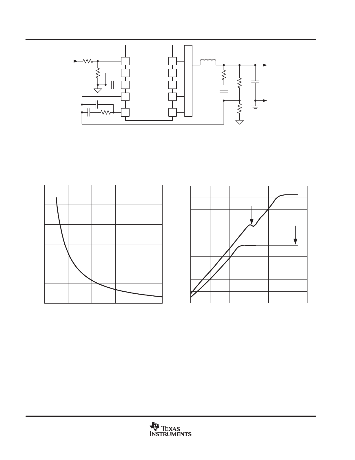
BP5 AND BP10 INTERNAL VOLTAGE REGULATORS
Start-up characteristics of the BP5 and BP10 regulators are shown in Figure 2. Slight variations in the BP5
occurs dependent upon the switching frequency. Variation in the BP10 regulation characteristics is also based
on the load presented by switching the external MOSFETs.
SELECTING THE INDUCTOR VALUE
The inductor value determines the magnitude of ripple current in the output capacitors as well as the load current
at which the converter enters discontinuous mode. Too large an inductance results in lower ripple current but
is physically larger for the same load current. Too small an inductance results in larger ripple currents and a
greater number of (or more expensive output capacitors for) the same output ripple voltage requirement. A good
compromise is to select the inductance value such that the converter doesn’t enter discontinuous mode until
the load approximated somewhere between 10% and 30% of the rated output. The inductance value is
described in equation (3).
where:.
D V
O
ǒ
VIN* V
L +
VIN DI f
is the output voltage
Ǔ
V
O
SW
O
(Henries)
D ∆I is the peak-to-peak inductor current
CALCULATING THE OUTPUT CAPACITANCE
The output capacitance depends on the output ripple voltage requirement, output ripple current, as well as any
output voltage deviation requirement during a load transient.
The output ripple voltage is a function of both the output capacitance and capacitor ESR. The worst case output
ripple is described in equation (4).
8 C
1
O
f
SW
Ǔ
V
ƫ
P*P
DV + DI
The output ripple voltage is typically between 90% and 95% due to the ESR component.
The output capacitance requirement typically increases in the presence of a load transient requirement. During
a step load, the output capacitance must provide energy to the load (light to heavy load step) or absorb excess
inductor energy (heavy to light load step) while maintaining the output voltage within acceptable limits. The
amount of capacitance depends on the magnitude of the load step, the speed of the loop and the size of the
inductor.
ESR )
ƪ
ǒ
www.ti.com
9

(5)
(6)
(7)
(8)
(9)
SLVS612 − APRIL 2006
APPLICATION INFORMATION
Stepping the load from a heavy load to a light load results in an output overshoot. Excess energy stored in the
inductor must be absorbed by the output capacitance. The energy stored in the inductor is described in
equation (5).
1
E
+
L I2(Joules)
L
2
where:
2
I
+
where:
D I
D I
Energy in the capacitor is described in equation (7).
where:
where:
D V
D V
Substituting equation (6) into equation (5), then substituting equation (8) into equation (7), then setting equation
(7) equal to equation (5), and then solving for C
is the output current under heavy load conditions
OH
is the output current under light load conditions
OL
E
+
C
2
V
+
is the final peak capacitor voltage
f
is the initial capacitor voltage
i
+
C
O
2
ǒ
Ǔ
ƪ
I
*
OH
1
C V2(Joules)
2
2
ǒ
Ǔ
ƪ
V
*
f
ǒ
ƪ
I
L
ǒ
ƪ
V
OH
Ǔ
f
2
ǒ
Ǔ
ǒ
(
ƫ
ƫ
V
ǒ
I
Ǔ
i
ǒ
Volts
OL
2
ƫ
Amperes
2
2
Ǔ
ƫ
I
OL
2
ǒ
Ǔ
V
i
2
Ǔ
*
2
ǒ
*
)
Ǔ
(Farads)
2
Ǔ
yields the capacitance described in equation (9).
O
10
www.ti.com

(10)
(11)
(12)
SLVS612 − APRIL 2006
APPLICATION INFORMATION
PROGRAMMING SOFT START
TPS40056 uses a closed-loop approach to ensure a controlled ramp on the output during start-up. Soft-start
is programmed by charging an external capacitor (C
on C
is closed on the lower of the C
rises above the external reference voltage, regulation is based on the external reference. To ensure a controlled
ramp-up of the output voltage the soft-start time should be greater than the L-C
in equation (10).
is fed into a separate non-inverting input to the error amplifier (in addition to FB and EA_REF). The loop
SS
voltage or the the external reference voltage EA_REF. Once the CSS voltage
SS
) via an internally generated current source. The voltage
SS
time constant as described
O
t
There is a direct correlation between t
the higher the input current required during start-up. This relationship is describe in more detail in the section
titled, Programming the Current Limit which follows. The soft-start capacitance, C
equation (11).
For applications in which the V
necessary to increase the soft-start time to between approximately 2 ms and 5 ms to prevent nuisance UVLO
tripping. The soft-start time should be longer than the time that the V
C
w 2p L C
START
2.3 mA
+
SS
0.7 V
Ǹ
t
START
(seconds)
O
and the input current required during start-up. The faster t
START
, is described in
SS
supply ramps up slowly, (typically between 50 ms and 100 ms) it may be
IN
supply transitions between 8 V and 9 V.
IN
(Farads)
PROGRAMMING CURRENT LIMIT
The TPS40056 uses a two-tier approach for overcurrent protection. The first tier is a pulse-by-pulse protection
scheme. Current limit is implemented on the high-side MOSFET by sensing the voltage drop across the
MOSFET when the gate is driven high. The MOSFET voltage is compared to the voltage dropped across a
resistor connected from VIN pin to the ILIM pin when driven by a constant current sink. If the voltage drop across
the MOSFET exceeds the voltage drop across the ILIM resistor, the switching pulse is immediately terminated.
The MOSFET remains off until the next switching cycle is initiated.
The second tier consists of a fault counter. The fault counter is incremented on an overcurrent pulse and
decremented on a clock cycle without an overcurrent pulse. When the counter reaches seven (7) a restart is
issued and seven soft-start cycles are initiated. Both the upper and lower MOSFETs are turned off during this
period. The counter is decremented on each soft-start cycle. When the counter is decremented to zero, the
PWM is re-enabled. If the fault has been removed the output starts up normally. If the output is still present the
counter counts seven overcurrent pulses and re-enters the second-tier fault mode. See Figure 3 for typical
overcurrent protection waveforms.
START
,
The minimum current limit setpoint (I
I
LIM
+
ǒ
CO V
ƪ
t
START
Ǔ
O
) IL(Amperes)
ƫ
) depends on t
LIM
www.ti.com
, CO, VO, and the load current at turn-on (IL).
START
11

(13)
SLVS612 − APRIL 2006
APPLICATION INFORMATION
The current limit programming resistor (R
the values used for V
the minimum value of I
I
+
OC
R
ILIM
OS
R
I
SINK
and I
SINK
DS(on)[max]
in the equation. In order to ensure the output current at the overcurrent level,
SINK
and the maximum value of VOS must be used.
V
)
I
SINK
where:
D I
D I
D V
is the current into the ILIM pin and is 8.6 µA, minimum
SINK
is the overcurrent setpoint which is the DC output current plus one-half of the peak inductor current
OC
is the overcurrent comparator offset and is 30 mV, maximum
OS
t
BLANKING
) is calculated using equation (13). Care must be taken in choosing
ILIM
OS
(W)
HDRV
CLOCK
V
ILIM
V
VIN−VSW
SS
(HDRV CYCLE TERMINATED BY CURRENT LIMIT
7 CURRENT LIMIT TRIPS
TRIP)
7 SOFT-START CYCLES
Figure 4. Typical Current Limit Protection Waveforms
SYNCHRONIZING TO AN EXTERNAL SUPPLY
The TPS40056 can be synchronized to an external clock through the SYNC pin. Synchronization occurs on the
falling edge of the SYNC signal. The synchronization frequency should be in the range of 20% to 30% higher
than its programmed free-run frequency. The clock frequency at the SYNC pin replaces the master clock
generated by the oscillator circuit. Pulling the SYNC pin low programs the TPS40056 to freely run at the
frequency programmed by R
.
T
UDG−02136
12
www.ti.com

(14)
(15)
(16)
(17)
(18)
(19)
SLVS612 − APRIL 2006
APPLICATION INFORMATION
LOOP COMPENSATION
Voltage-mode buck-type converters are typically compensated using Type III networks. Since the TPS40056
includes no voltage feedforward control, the gain of the PWM modulator must be included. The modulator gain
is described in Figure 5.
A
MOD
+
V
IN
or A
V
S
MOD(dB)
+ 20 log
V
IN
ǒ
Ǔ
V
S
Duty dycle, D, varies from 0 to 1 as the control voltage, VC, varies from the minimum ramp voltage to the
maximum ramp voltage, V
. Also, for a synchronous buck converter, D = VO / VIN. To get the control voltage
S
to output voltage modulator gain in terms of the input voltage and ramp voltage,
V
D +
V
O
V
IN
+
C
V
S
or
V
V
O
IN
+
V
V
C
S
Calculate the Poles and Zeros
For a buck converter using voltage mode control there is a double pole due to the output L-C
. The double pole
O
is located at the frequency calculated in equation (16).
+
f
LC
2p L C
There is also a zero created by the output capacitance, C
1
Ǹ
O
(Hertz)
, and its associated ESR. The ESR zero is located
O
at the frequency calculated in equation (17).
+
V
V
OUT
1
EA_REF
* V
(Hertz)
O
to set the output voltage, V
BIAS
R1
W
EA_REF
OUT
.
f
+
Z
2p ESR C
Calculate the value of R
R
BIAS
The maximum crossover frequency (0 dB loop gain) is calculated in equation (19).
f
SW
+
f
C
Typically, f
(Hertz)
4
is selected to be close to the midpoint between the L-CO double pole and the ESR zero. At this
C
frequency, the control to output gain has a –2 slope (−40 dB/decade), while the Type III topology has a +1 slope
(20 dB/decade), resulting in an overall closed loop –1 slope (−20 dB/decade).
Figure 5 shows the modulator gain, L-C filter, output capacitor ESR zero, and the resulting response to be
compensated.
www.ti.com
13

PWM MODULATOR RELATIONSHIPS
SLVS612 − APRIL 2006
APPLICATION INFORMATION
V
S
V
D = VC / V
MODULATOR GAIN
vs
SWITCHING FREQUENCY
ESR Zero, + 1
A
= VIN / V
MOD
C
Modulator Gain − dB
S
100 1 k 10 k 100 k
Figure 5
S
Resultant, − 1
LC Filter, − 2
fSW − Switching Frequency − Hz
Figure 6
A Type III topology, shown in Figure 7, has two zero-pole pairs in addition to a pole at the origin. The gain and
phase boost of a T ype III topology is shown in Figure 8. The two zeros are used to compensate the L-C
pole and provide phase boost. The double pole is used to compensate for the ESR zero and provide controlled
gain roll-off. In many cases the second pole can be eliminated and the amplifier’s gain roll-off used to roll-off
the overall gain at higher frequencies.
C2
(optional)
C3
VOUT
R1
R3
R
C1
VFB
7
BIAS
EA_REF
R2
8
+
Figure 7. Type III Compensation Configuration
COMP
UDG−03099
0 dB
−90°
−270°
Figure 8. Type III Compensation Gain and Phase
− 1
+ 1
GAIN
180°
PHASE
double
O
− 1
14
www.ti.com

(20)
(21)
(22)
(23)
(24)
(25)
APPLICATION INFORMATION
The poles and zeros for a type III network are described in equations (20).
SLVS612 − APRIL 2006
f
+
Z1
2p R2 C1
+
f
P1
The value of R1 is somewhat arbitraty, but influences other component values. A value between 50 kΩ and
100 kΩ usually yields reasonable values.
The unity gain frequency is described in equation (21)
f
+
C
2p R1 C2 G
where G is the reciprocal of the modulator gain at f
The modulator gain as a function of frequency at f
AMOD(f) + AMOD
Minimum Load Resistance
Care must be taken not to load down the output of the error amplifier with the feedback resistor, R2, that is too
small. The error amplifier has a finite output source and sink current which must be considered when sizing R2.
Too small a value does not allow the output to swing over its full range.
R2
(MIN)
1
1
2p R2 C2
1
V
+
C(max)
I
SOURCE (min)
(Hertz) f
(Hertz) f
(Hertz)
2
f
LC
ǒ
Ǔ
C
+
and G +
3.45 V
2mA
f
+
Z2
+
P2
AMOD(f)
+ 1725 W
1
2p R1 C3
1
2p R3 C3
.
C
, is described in equation (22).
C
1
(Hertz)
(Hertz)
CALCULATING THE BOOST AN BP10 BYPASS CAPACITOR
The BOOST capacitance provides a local, low impedance source for the high-side driver. The BOOST capacitor
should be a good quality, high-frequency capacitor. The size of the bypass capacitor depends on the total gate
charge of the MOSFET and the amount of droop allowed on the bypass capacitor. The BOOST capacitance
is described in equation (24).
Q
+
+
g
(Farads)
DV
ǒ
Q
) Q
gHS
DV
gSR
Ǔ
(Farads)
C
BOOST
The 10-V reference pin, BP10V needs to provide energy for both the synchronous MOSFET and the high-side
MOSFET via the BOOST capacitor. Neglecting any efficiency penalty, the BP10V capacitance is described in
equation (25).
C
BP10
www.ti.com
15

(26)
(27)
(28)
SLVS612 − APRIL 2006
APPLICATION INFORMATION
dv/dt Induced Turn−On
MOSFETs are susceptible to dv/dt turn-on particularly in high-voltage (VDS) applications. The turn-on is caused
by the capacitor divider that is formed by C
the MOSFET causes current flow through C
gate-to-source voltage rises above the MOSFET threshold voltage, the MOSFET turns on, resulting in large
shoot-through currents. Therefore, the SR MOSFET should be chosen so that the C
than the C
capacitance.
GS
High Side MOSFET Power Dissipation
The power dissipated in the external high-side MOSFET is comprised of conduction and switching losses. The
conduction losses are a function of the I
high-side MOSFET conduction losses are defined by equation (26).
2
ǒ
I
RMS
Ǔ
R
DS(on)
where:
P
COND
+
RMS
ǒ
and CGS. High dv/dt conditions and drain-to-source voltage, on
GD
current through the MOSFET and the R
1 ) TC
and causes the gate-to-source voltage to rise. If the
GD
capacitance is smaller
GD
of the MOSFET. The
DS(on)
R
ƪ
TJ* 25
ƫ
Ǔ
(Watts)
D TC
The TCR varies depending on MOSFET technology and manufacturer but is typically ranges between
.0035 ppm/_C and .010 ppm/_C.
The I
The switching losses for the high-side MOSFET are descibed in equation (28).
where:
D I
D t
D f
Typical switching waveforms are shown in Figure 8.
is the temperature coefficient of the MOSFET R
R
current for the high side MOSFET is described in equation (27).
RMS
Ǹ
ǒ
VIN I
ǒ
Amperes
t
OUT
+ IO d
I
RMS
P
SW(fsw)
is the DC output current
O
is the switching rise time, typically < 20 ns
SW
is the switching frequency
SW
+
Ǔ
RMS
Ǔ
fSW(Watts)
SW
DS(on)
16
www.ti.com

9
I
I
(29)
(30)
(31)
(32)
SLVS612 − APRIL 2006
APPLICATION INFORMATION
D2
I
O
d 1−d
I
D1
}
∆
BODY DIODE
CONDUCTION
SW
0
ANTI−CROSS
CONDUCTION
SYNCHRONOUS
RECTIFIER ON
BODY DIODE
CONDUCTION
HIGH SIDE ON
Figure 9. Inductor Current and SW Node Waveforms
The maximum allowable power dissipation in the MOSFET is determined by equation (29).
ǒ
TJ* T
+
P
T
Ǔ
A
q
JA
(Watts)
where:
P
and θ
+ P
T
is the package thermal impedance.
JA
COND
) P
SW(fsw)
(Watts)
UDG−0213
Synchronous Rectifier MOSFET Power Dissipation
The power dissipated in the synchronous rectifier MOSFET is comprised of three components: R
conduction losses, body diode conduction losses, and reverse recovery losses. R
be found using equation (32) and the RMS current through the synchronous rectifier MOSFET is described in
equation (31).
I
+ IO 1 * d
RMS
Ǹ
ǒ
Amperes
RMS
Ǔ
The body-diode conduction losses are due to forward conduction of the body diode during the anti−cross
conduction delay time. The body diode conduction losses are described by equation (32).
P
+ 2 IO VF t
DC
DELAY
f
SW
(Watts)
where:
D V
is the body diode forward voltage
F
D t
is the total delay time just before the SW node rises.
DELAY
www.ti.com
) conduction losses can
DS(on
DS(on)
17

(33)
(34)
(35)
(36)
(37)
(38)
SLVS612 − APRIL 2006
APPLICATION INFORMATION
The 2-multiplier is used because the body-diode conducts twice each cycle (once on the rising edge and once
on the falling edge). The reverse recovery losses are due to the time it takes for the body diode to recovery from
a forward bias to a reverse blocking state. The reverse recovery losses are described in equation (33).
P
where:
+ 0.5 QRR VIN f
RR
SW
(Watts)
D Q
The total synchronous rectifier MOSFET power dissipation is described in equation (34).
TPS40056 POWER DISSIPATION
The power dissipation in the TPS40056 is largely dependent on the MOSFET driver currents and the input
voltage. The driver current is proportional to the total gate charge, Qg, of the external MOSFETs. Driver power
(neglecting external gate resistance, refer to [2] can be calculated from equation (35).
And the total power dissipation in the TPS40056, assuming the same MOSFET is selected for both the high-side
and synchronous rectifier is described in equation (36).
or
where:
D I
The maximum power capability of the device’s PowerPad package is dependent on the layout as well as air flow.
The thermal impedance from junction to air, assuming 2 oz. copper trace and thermal pad with solder and no
air flow.
is the reverse recovery charge of the body diode
RR
+ PDC) PRR) P
P
SR
P
+ Qg VDR f
D
2 P
ǒ
+
P
T
ǒ
P
+
T
is the quiescent operating current (neglecting drivers)
Q
D
) I
V
DR
2 Qg fSW) I
COND
SW
Ǔ
VIN(Watts)
Q
(Watts)
(Watts)
Ǔ
VIN(Watts)
Q
θ
= 36.51°C/W
JA
The maximum allowable package power dissipation is related to ambient temperature by equation (29).
Substituting equation (29) into equation (37) and solving for f
the TPS4005x. The result is described in equation (38).
18
f
SW
+
ǒ
ǒ
TJ*T
ƪ
ǒ
q
JA VDD
ǒ
2 Q
Ǔ
A
ƫ
* I
Ǔ
Q
Ǔ
Ǔ
g
(Hz)
www.ti.com
yields the maximum operating frequency for
SW

SLVS612 − APRIL 2006
LAYOUT CONSIDERATIONS
The PowerPADt package
The PowerPAD package provides low thermal impedance for heat removal from the device. The PowerPAD
derives its name and low thermal impedance from the large bonding pad on the bottom of the device. For
maximum thermal performance, the circuit board must have an area of solder-tinned-copper underneath the
package. The dimensions of this area depends on the size of the PowerPAD package. For a 16-pin TSSOP
(PWP) package the area is 5 mm x 3.4 mm [3].
Thermal vias connect this area to internal or external copper planes and should have a drill diameter sufficiently
small so that the via hole is effectively plugged when the barrel of the via is plated with copper. This plug is
needed to prevent wicking the solder away from the interface between the package body and the solder-tinned
area under the device during solder reflow. Drill diameters of 0.33 mm (13 mils) works well when 1-oz copper
is plated at the surface of the board while simultaneously plating the barrel of the via. If the thermal vias are not
plugged when the copper plating is performed, then a solder mask material should be used to cap the vias with
a diameter equal to the via diameter of 0.1 mm minimum. This capping prevents the solder from being wicked
through the thermal vias and potentially creating a solder void under the package. Refer to PowerPAD Thermally
Enhanced Package
PowerPAD package.
[3]
and the mechanical illustration at the end of this document for more information on the
X: Minimum PowerPAD = 1.8 mm
Y: Minimum PowerPAD = 1.4 mm
X
4,50 mm
4,30 mm
Y
101
6,60 mm
6,20 mm
Thermal Pad
Figure 10. PowerPAD Dimensions
MOSFET Packaging
MOSFET package selection depends on MOSFET power dissipation and the projected operating conditions.
In general, for a surface-mount applications, the DPAK style package provides the lowest thermal impedance
(θ
) and, therefore, the highest power dissipation capability. However, the effectiveness of the DPAK depends
JA
on proper layout and thermal management. The θ
copper area and thickness. In most cases, a lowest thermal impedance of 40°C/W requires one square inch
of 2-ounce copper on a G−10/FR−4 board. Lower thermal impedances can be achieved at the expense of board
area. Please refer to the selected MOSFET’s data sheet for more information regarding proper mounting.
specified in the MOSFET data sheet refers to a given
JA
www.ti.com
19

SLVS612 − APRIL 2006
LAYOUT CONSIDERATIONS
Grounding and Circuit Layout Considerations
The TPS4005x provides separate signal ground (SGND) and power ground (PGND) pins. It is important that
circuit grounds are properly separated. Each ground should consist of a plane to minimize its impedance if
possible. The high power noisy circuits such as the output, synchronous rectifier, MOSFET driver decoupling
capacitor (BP10), and the input capacitor should be connected to PGND plane at the input capacitor.
Sensitive nodes such as the FB resistor divider, R
SGND plane should only make a single point connection to the PGND plane.
Component placement should ensure that bypass capacitors (BP10 and BP5) are located as close as possible
to their respective power and ground pins. Also, sensitive circuits such as FB, R T and ILIM should not be located
near high dv/dt nodes such as HDRV, LDRV, BOOST, and the switch node (SW).
The SW pin Schottky diode, D2 in Figure 10, should be placed close to the TPS40056 with short, wide traces
to pins 9 and 12.
, and ILIM should be connected to the SGND plane. The
T
20
www.ti.com

(39)
(40)
(41)
(42)
(43)
D Input Voltage: 10 Vdc to 14.4 Vdc
SLVS612 − APRIL 2006
DESIGN EXAMPLE
D Output voltage: 1.25 V ±1% (1.2375 ≤ V
≤1.2625)
O
D Output current: 8 A (maximum, steady state), 10 A (surge, 10ms duration, 10% duty cycle maximum)
D Output ripple: 33 mV
P-P
at 8 A
D Output load response: 0.1 V => 10% to 90% step load change, from 1 A to 7 A
D Operating temperature: −40°C to 85°C
D f
1. Calculate maximum and minimum duty cycles
d
2. Select switching frequency
The switching frequency is based on the minimum duty cycle ratio and the propagation delay of the current limit
comparator. I n order to maintain current limit capability, the on time of the upper MOSFET , t
than 400 ns (see Electrical Characteristics table). Therefore
MIN
=170 kHz
SW
V
+
V
V
O(min)
V
IN(max)
1
T
SW
O(min)
IN(max)
+
+ f
SW
+
T
t
ON
SW
+
1.2375
14.4
V
ȡ
ǒ
V
ȧ
ȧ
ȧ
ȧ
Ȣ
+ 0.086 d
or
ON
ȣ
Ǔ
ȧ
ȧ
ȧ
ȧ
O(min)
IN(max)
T
Ȥ
MAX
+
V
O(max)
V
IN(min)
+
1.2625
10
+ 0.126
, must be greater
ON
Using 450 ns to provide margin,
0.086
+
f
SW
450 ns
Since the oscillator can vary by 10%, decrease f
fSW+ 0.9 191 kHz + 172 kHz
and therefore choose a frequency of 170 kHz.
3. Select ∆I
In this case ∆I is chosen so that the converter enters discontinuous mode at 20% of nominal load.
DI + I
O
+ 191 kHz
2 0.2 + 8 2 0.2 + 3.2 A
www.ti.com
, by 10%
SW
21

P
DC
I
O
V
FD
t
DELAY
f
SW
8.0 A 0.8 V 100 ns 170 kHz+0.218 W
(44)
(45)
(46)
(47)
(48)
(49)
(50)
(51)
(52)
(53)
SLVS612 − APRIL 2006
4. Calculate the power losses
DESIGN EXAMPLE
Power losses in the high-side MOSFET (Si7860DP) at 14.4-V
where switching losses dominate can be
IN
calculated from equation (27).
I
+ IO dǸ+ 8 0.086Ǹ+ 2.35 A
RMS
substituting (27) into (26) yields
P
+ 2.352 0.008 (1 ) 0.007 (150 * 25))+ 0.083 W
COND
and from equation (28), the switching losses can be determined.
P
SW(fsw)
ǒ
+
VIN IO t
Ǔ
fSW+ 14.4 V 8A 20 ns 170 kHz + 0.39 W
SW
The MOSFET junction temperature can be found by substituting equation (30) into equation (29)
ǒ
T
+
P
J
COND
) P
SW
Ǔ
q
JA
) T
(
+
0.083 ) 0.39) 40 ) 85 + 90OC
A
5. Calculate synchronous rectifier losses
The synchronous rectifier MOSFET has two loss components, conduction, and diode reverse recovery losses.
The conduction losses are due to I
losses as well as body diode conduction losses during the dead time
RMS
associated with the anti-cross conduction delay.
The I
current through the synchronous rectifier from (31)
RMS
I
+ IO 1 * dǸ+ 8 1 * 0.126Ǹ+ 7.48 A
RMS
RMS
The synchronous MOSFET conduction loss from (26) is:
P
+ 7.482 0.008 (1 ) 0.007(150 * 25))+ 0.83 W
COND
The body diode conduction loss from (32) is:
+2
+2
The body diode reverse recovery loss from (33) is:
P
+ 0.5 QRR VIN fSW+ 0.5 30 nC 14.4 V 170 kHz + 0.037 W
RR
The total power dissipated in the synchronous rectifier MOSFET from (34) is:
+ PRR) P
P
SR
) PDC+ 0.037 ) 0.83 ) 0.218 + 1.085 W
COND
The junction temperature of the synchronous rectifier at 85°C is:
+ P
T
J
SR
q
JA
) T
(
+
1.085) 40 ) 85 + 128oC
A
In typical applications, paralleling the synchronous rectifier MOSFET with a Schottky rectifier increases the
overall converter efficiency by approximately 2% due to the lower power dissipation during the body diode
conduction and reverse recovery periods.
22
www.ti.com

(54)
(55)
(56)
(57)
(58)
(59)
DESIGN EXAMPLE
6. Calculate the inductor value
The inductor value is calculated from equation (3).
(
14.4 * 1.25 V) 1.25 V
L +
14.4 V 3.2 A 170 kHz
A 2.9-µH Coev DXM1306−2R9 or 2.6-µH Panasonic ETQ−P6F2R9LFA can be used.
7. Setting the switching frequency
+ 2.1 mH
SLVS612 − APRIL 2006
The clock frequency is set with a resistor (R
equation (1), with f
R
+ ǒ
T
f
SW
8. Calculating the output capacitance (C
In this example the output capacitance is determined by the load response requirement of ∆V = 0.1 V for a 1 A
to 7 A step load. C
2.9 m
+
C
O
Using (4) we can calculate the ESR required to meet the output ripple requirements.
33 mV + 3.2 A
ESR + 10.3 mW * 1.0 mW + 9.3 mW
For this design example two (2) Panasonic SP EEFUEOD471R capacitors, (2.0 V, 470 µF, 12 mΩ) are used.
9. Calculate the soft-start capacitor (C
This design requires a soft−start time (t
SS
+
2.3 mA
0.7 V
C
in kHz.
SW
1
17.82 10
can be calculated using (9)
O
2
ǒ
(8A)
*
ǒ
2
(
)
1.25
(
*
1.15
ǒ
ESR )
1ms+ 3.29 nF + 3300 pF
* 23ǓkW + 307 kW N use 309 kW
*6
O
2
Ǔ
(1A)
2
Ǔ
)
8 761 mF 170 kHz
SS
) from the RT pin to ground. The value of RT can be found from
T
)
+ 761 mF
1
)
START
) of 1 ms. CSS can be calculated on (11)
Ǔ
www.ti.com
23

(60)
(61)
(62)
(63)
(64)
(65)
(66)
SLVS612 − APRIL 2006
DESIGN EXAMPLE
10. Calculate the current limit resistor (R
The current limit set point depends on t
design,
I
For this design, set I
plus one-half the ripple current of 3.2 A and R
R
11. Calculate loop compensation values
Calculate the DC modulator gain (A
A
Calculate the output filter L-C
f
and
f
940 mF 1.25 V
u
LIM
12.6 A 0.0104W
+
ILIM
12
+
MOD
+
LC
Z
+
Ǹ
2p L C
2p ESR C
1ms
for 1 1.0 ADC minimum. From equation (13), with IOC equal to the DC output surge current
LIM
8.6 mA
+ 6.0 A
2
1
O
1
) 8.0 A + 9.2 A
)
MOD
MOD(dB)
poles and C
O
+
Ǹ
2p 2.9 mH 940 mF
+
2p 0.006 940 mF
O
)
ILIM
, VO,CO and I
START
is increased 30% (1.3 * 0.008) to allow for MOSFET heating.
DS(on)
(0.03)
8.6 mA
+ 15.24 kW * 3.5 kW + 11.74 kW ^ 11.8 W
) from equation (14)
+ 20 log(6)+ 15.6 dB
ESR zeros from (16) and (17)
O
1
1
+ 3.05 kHz
+ 28.2 kHz
at start-up as shown in equation (12). For this
LOAD
Select the close-loop 0 dB crossover frequency, fC. For this example fC = 20 kHz.
Select the double zero location for the T ype III compensation network at the output filter double pole at 3.05 kHz.
Select the double pole location for the Type III compensation network at the output capacitor ESR zero at
28.2 kHz.
The amplifier gain at the crossover frequency of 20 kHz is determined by the reciprocal of the modulator gain
AMOD at the crossover frequency from equation (22).
A
And also from equation (22).
G +
Choose R1 = 100 kΩ
MOD(f)
A
+ A
1
MOD(f)
MOD
+
1
0.14
ǒ
2
f
LC
Ǔ
f
C
+ 7.14
+ 6
3.05 kHz
ǒ
20 kHz
2
Ǔ
+ 0.14
24
www.ti.com

(67)
(68)
(69)
(70)
(71)
(72)
(73)
DESIGN EXAMPLE
The poles and zeros for a type III network are described in equations (20) and (21).
SLVS612 − APRIL 2006
f
+
Z2
2p R1 C3
+
f
P2
2p R3 C3
f
+
C
2p R1 C2 G
+
f
P1
2p R2 C2
f
+
Z1
2p R2 C1
Calculate the value of R
1
1
1
1
1
N C3 +
N R3 +
N R2 +
N C1 +
from equation (17) with R1 = 100 kΩ. Since the output of 1.25-V is within the
BIAS
2p 100 kW 3.05 kHz
2p 560 pF 28.2 kHz
N C2 +
2p 100 kW 7.14 20 kHz
2p 10 pF 28.2 kHz
2p 562 kW 3.05 kHz
EA_REF input specification of 0.5 V to 1.5 V, an R
1
1
+ 522 pF, choose 560 pF
+ 10.08 kW, choose 10 kW
1
1
1
BIAS
+ 564 kW, choose 562 kW
+ 92.9 pF, choose 100 pF
resistor is not required.
+ 11.1 pF, choose 10 pF
CALCULATING THE BOOST AND BP10V BYPASS CAPACITANCE
The size of the bypass capacitor depends on the total gate charge of the MOSFET being used and the amount
of droop allowed on the bypass cap. The BOOST capacitance for the Si7860DP, allowing for a 0.5 voltage droop
on the BOOST pin from equation (24) is:
Q
g
C
BOOST
+
DV
+
18 nC
0.5 V
+ 36 nF
and the BP10V capacitance from (25) is
C
BP(10 V)
+
Q
gHS
gSR
DV
+
2 Q
DV
g
36 nC
+
0.5 V
+ 72 nF
) Q
For this application, a 0.1-µF capacitor is used for the BOOST bypass capacitor and a 1.0-µF capacitor is used
for the BP10V bypass.
Figure 10 show s c omponent selection for the 10-V to 14.4-V to 1.25-V at 8 A dc-to-dc converter specified in the
design example.
REFERENCES
1. Balogh, Laszlo, Design and Application Guide for High Speed MOSFET Gate Drive Circuits, Texas
Instruments/Unitrode Corporation, Power Supply Design Seminar, SEM−1400 Topic 2.
2. PowerPAD Thermally Enhanced Package Texas Instruments, Semiconductor Group, Technical Brief: TI
Literature No. SLMA002
www.ti.com
25

SLVS612 − APRIL 2006
100 pF
11.8 kΩ
+
TT
V
470 µF
470 µF
R1
100 kΩ
50 V
22 µF
50 V
22 µF
50 V
1.0 µF
0.1 µF
2.9 µH
Si7860DP
R3
10 kΩ
3.3 Ω
D2
SW
R
C3
D1
−
560 pF
Si7860DP
1.0 µF
R2
10
LDRV
VFB
7
562 kΩ
100 pF
9
PGND
PWP
COMP
8
C2
10 pF
C1
16
15
14
13
12
11
VIN
ILIM
BOOST
TPS40056PWP
SYNC
RT
BP5
1
2
3
330 µF
R4
1.0 µF
10 kΩ
T
R
165 kΩ
330 µF
TRKIN
IN
+
V
−
V
SW
HDRV
EA_REF
SGND
4
5
SS
C
R5
BP10
SS
6
3300 pF
10 kΩ
Figure 11. 12-V to 1.25-V at 8-A DC-to-DC Converter (DDR) Design Example
UDG−03100
26
www.ti.com

SLVS612 − APRIL 2006
Center Power Pad Solder Stencil Opening
Stencil Thickness X Y
0.1mm
0.127mm
0.152mm
0.178mm
2.5 2.65
2.31 2.46
2.15 2.3
2.05 2.15
www.ti.com
27


IMPORTANT NOTICE
Texas Instruments Incorporated and its subsidiaries (TI) reserve the right to make corrections, modifications,
enhancements, improvements, and other changes to its products and services at any time and to discontinue
any product or service without notice. Customers should obtain the latest relevant information before placing
orders and should verify that such information is current and complete. All products are sold subject to TI’s terms
and conditions of sale supplied at the time of order acknowledgment.
TI warrants performance of its hardware products to the specifications applicable at the time of sale in
accordance with TI’s standard warranty. Testing and other quality control techniques are used to the extent TI
deems necessary to support this warranty . Except where mandated by government requirements, testing of all
parameters of each product is not necessarily performed.
TI assumes no liability for applications assistance or customer product design. Customers are responsible for
their products and applications using TI components. To minimize the risks associated with customer products
and applications, customers should provide adequate design and operating safeguards.
TI does not warrant or represent that any license, either express or implied, is granted under any TI patent right,
copyright, mask work right, or other TI intellectual property right relating to any combination, machine, or process
in which TI products or services are used. Information published by TI regarding third-party products or services
does not constitute a license from TI to use such products or services or a warranty or endorsement thereof.
Use of such information may require a license from a third party under the patents or other intellectual property
of the third party, or a license from TI under the patents or other intellectual property of TI.
Reproduction of information in TI data books or data sheets is permissible only if reproduction is without
alteration and is accompanied by all associated warranties, conditions, limitations, and notices. Reproduction
of this information with alteration is an unfair and deceptive business practice. TI is not responsible or liable for
such altered documentation.
Resale of TI products or services with statements different from or beyond the parameters stated by TI for that
product or service voids all express and any implied warranties for the associated TI product or service and
is an unfair and deceptive business practice. TI is not responsible or liable for any such statements.
Following are URLs where you can obtain information on other Texas Instruments products and application
solutions:
Products Applications
Amplifiers amplifier.ti.com Audio www.ti.com/audio
Data Converters dataconverter.ti.com Automotive www.ti.com/automotive
DSP dsp.ti.com Broadband www.ti.com/broadband
Interface interface.ti.com Digital Control www.ti.com/digitalcontrol
Logic logic.ti.com Military www.ti.com/military
Power Mgmt power.ti.com Optical Networking www.ti.com/opticalnetwork
Microcontrollers microcontroller.ti.com Security www.ti.com/security
Low Power Wireless www.ti.com/lpw Telephony www.ti.com/telephony
Video & Imaging www.ti.com/video
Wireless www.ti.com/wireless
Mailing Address: Texas Instruments
Post Office Box 655303 Dallas, Texas 75265
Copyright 2006, Texas Instruments Incorporated
 Loading...