

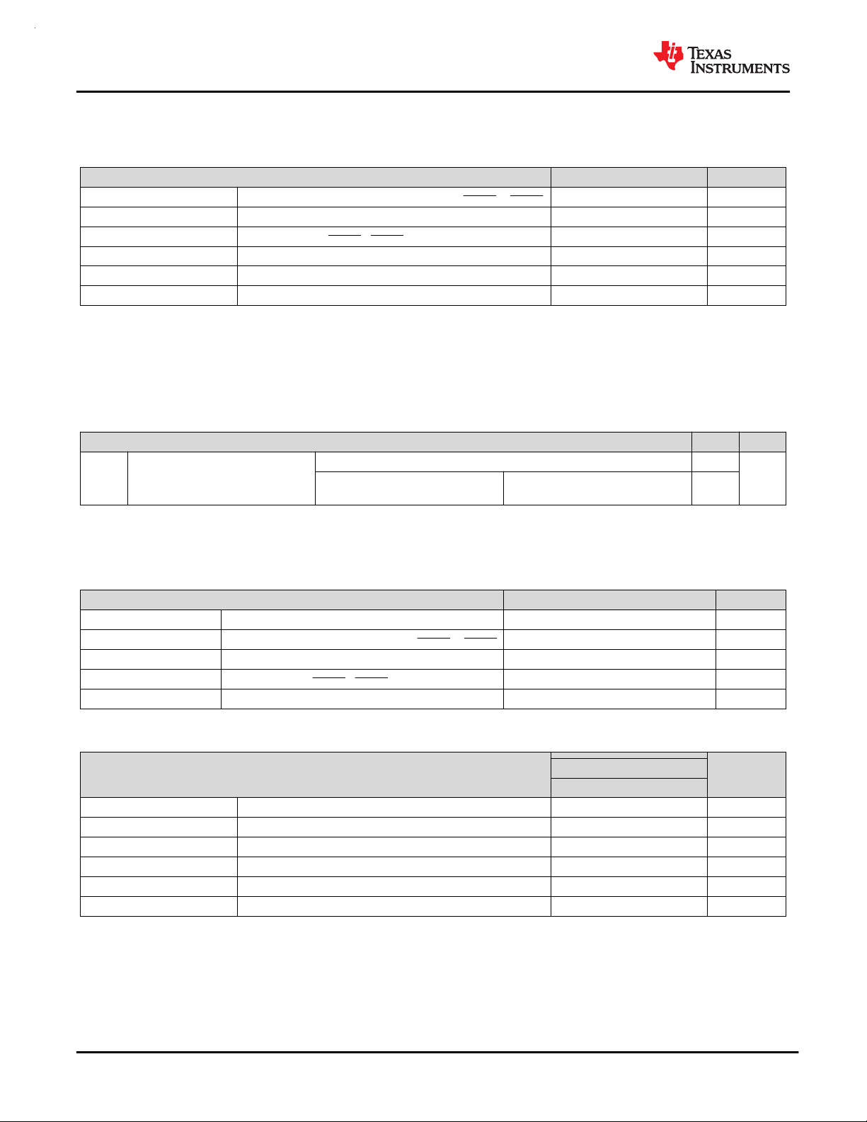
DC/DC
MCU
Low Iq, No external
resistors needed
GND
Boost
Converter
MCU Flag
Enable
Boost
SENSE1
SENSE2
RESET1
RESET2
Backup
Vbatt
VDD
GND
VDD
GPIO
TPS38A
Supply Voltage (V)
Quiescent Current (µA)
0 5 10 15 20 25 30 35 40 45 50 55 60 65
0.5
0.55
0.6
0.65
0.7
0.75
0.8
0.85
0.9
0.95
1
IqNO
125 C
25 C
85 C
-40 C
www.ti.com
ADVANCE INFORMATION
SNVSBI8A – AUGUST 2020 – REVISED JANUARY 2021
SNVSBI8A – AUGUST 2020 – REVISED JANUARY 2021
TPS38x -Q1 (65 V & 2uA) Wide VIN Dual Channel Voltage Detector
TPS38X-Q1
TPS38X-Q1
1 Features
• AEC-Q100 qualified with the following results:
– Device temperature grade 1: –40°C to +125°C
ambient operating temperature
– Device HBM ESD classification level 2
– Device CDM ESD classification level C7B
• VDD: 2.7 V to 65 V (V
POR
=1.4 V)
• SENSE and RESET pins are 65 V graded
• Low supply current: 1 μA (Typ.)
• Flexible voltage option Table 14-2
– 2.7 V to 36 V (1.5% max accuracy)
– 800 mV option (1% max accuracy)
• Built-in hysteresis (V
HYS
)
– Percentage options: 2% to 13% (1% steps)
– Fixed options: VTH < 8 V = 0.5 V, 1 V, 1.5 V,
2 V, 2.5 V
• Programmable reset time delay
– 10 nF = 12.8 ms, 10 μF = 12.8 s
• Programmable sense time delay
– 10 nF = 1.28 ms, 10 μF = 1.28 s
• Manual reset feature
• Output reset latching feature
• Output topology:
– Channel 1: Open-Drain or Push-Pull topologies
– Channel 2: Open-Drain
2 Applications
• Telematics control unit
• Emergency call system
• Audio amplifier
• Head unit and cluster
• Sensor fusion and cameras
• Body control module
3 Description
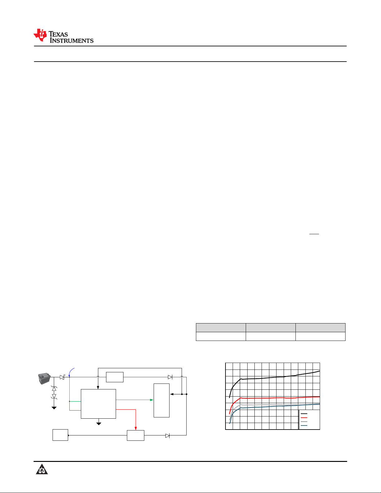
The TPS38x-Q1 is a 65 V-input voltage detector with
1 μA IDD, 1% accuracy, and 10 μs detection time in a
6.25 mm2 package. This device can be connected
directly to 12 V / 24 V automotive battery system for
continous monitoring of over (OV) and under (UV)
voltage conditions; with its internal resistor divider, it
offers the smallest total solution size. Wide hysteresis
voltage options are available to ignore cold crank,
start-stop and various car battery voltage transients.
Built-in hysteresis on the SENSE pins prevents false
reset signals when monitoring a supply voltage rail.
The separate VDD and SENSE pins allow for the
redundancy sought by high-reliability automotive
systems and SENSE can monitor higher and lower
voltages than VDD. Optional use of external resistors
are supported by the high impedance input of the
SENSE pins. Both CTSx and CTRx provide delay
adjustability on the rising and falling edges of the
RESET signals. Also, CTSx functions as a debouncer
by ignoring voltage glitches on the monitored voltage
rails; CTRx operates as a manual reset (MR) that can
be used to force a system reset.
The TPS38x-Q1 is available in a small 2.5-mm×2.5mm×0.1-mm WSON 10-pin wettable flanks package
allowing the facillitation for Automatic Optical
Inspection (AOI) and low resolution X-ray inspection.
The central pad is non-conductive to increase the
creepage between VDD and GND per guidelines in
IEC60664. TPS38x-Q1 operates over –40°C to
+125°C (TA).
Device Information
PART NUMBER PACKAGE
TPS38x-Q1 WSON-10 (DSK) 2.5 mm × 2.5 mm
(1) For package details, see the mechanical drawing addendum
at the end of the data sheet.
(1)
BODY SIZE (NOM)
An IMPORTANT NOTICE at the end of this data sheet addresses availability, warranty, changes, use in safety-critical applications,
Copyright © 2021 Texas Instruments Incorporated
intellectual property matters and other important disclaimers. ADVANCE INFORMATION for preproduction products; subject to change
without notice.
Typical Application Circuit
Typical Supply Current vs VDD
Product Folder Links: TPS38X-Q1
Submit Document Feedback
1

TPS38X-Q1
ADVANCE INFORMATION
SNVSBI8A – AUGUST 2020 – REVISED JANUARY 2021
www.ti.com
Table of Contents
1 Features............................................................................1
2 Applications..................................................................... 1
3 Description.......................................................................1
4 Revision History.............................................................. 2
5 Device Comparison......................................................... 3
6 Pin Configuration and Functions...................................4
7 Specifications.................................................................. 8
7.1 Absolute Maximum Ratings ....................................... 8
7.2 ESD Ratings .............................................................. 8
7.3 Recommended Operating Conditions ........................8
7.4 Thermal Information ...................................................8
7.5 Electrical Characteristics ............................................9
7.6 Timing Requirements ............................................... 11
8 Typical Characteristics................................................. 12
9 Detailed Description......................................................13
9.1 Overview................................................................... 13
9.2 Functional Block Diagram......................................... 13
9.3 Feature Description...................................................14
10 Device Functional Modes........................................... 21
11 Application and Implementation................................ 22
11.1 Adjustable Voltage Thresholds................................22
11.2 Application Information............................................22
11.3 Typical Application.................................................. 23
12 Power Supply Recommendations..............................25
12.1 Power Dissipation and Device Operation............... 25
13 Layout...........................................................................26
13.1 Layout Guidelines................................................... 26
13.2 Layout Example...................................................... 26
13.3 Creepage Distance................................................. 26
14 Device and Documentation Support..........................27
14.1 Device Nomenclature..............................................27
14.2 Support Resources................................................. 29
14.3 Trademarks.............................................................29
14.4 Electrostatic Discharge Caution..............................29
14.5 Glossary..................................................................29
15 Mechanical, Packaging, and Orderable
Information.................................................................... 29
4 Revision History
NOTE: Page numbers for previous revisions may differ from page numbers in the current version.
Changes from Revision * (August 2020) to Revision A (January 2021) Page
• APL Update........................................................................................................................................................ 1
• Added Typical Supply Current vs VDD Curve and modified Description section............................................... 1
• Edited both Power Cycle figures (SENSE Outside and Within Nominal Voltage)............................................ 14
• Corrected the Hysteresis titles for both Undervoltage figures.......................................................................... 16
• Added reset time delay discharge guideline..................................................................................................... 18
• Added sense time delay discharge guideline................................................................................................... 19
• Added Device Functional Modes tables........................................................................................................... 21
2 Submit Document Feedback
Copyright © 2021 Texas Instruments Incorporated
Product Folder Links: TPS38X-Q1
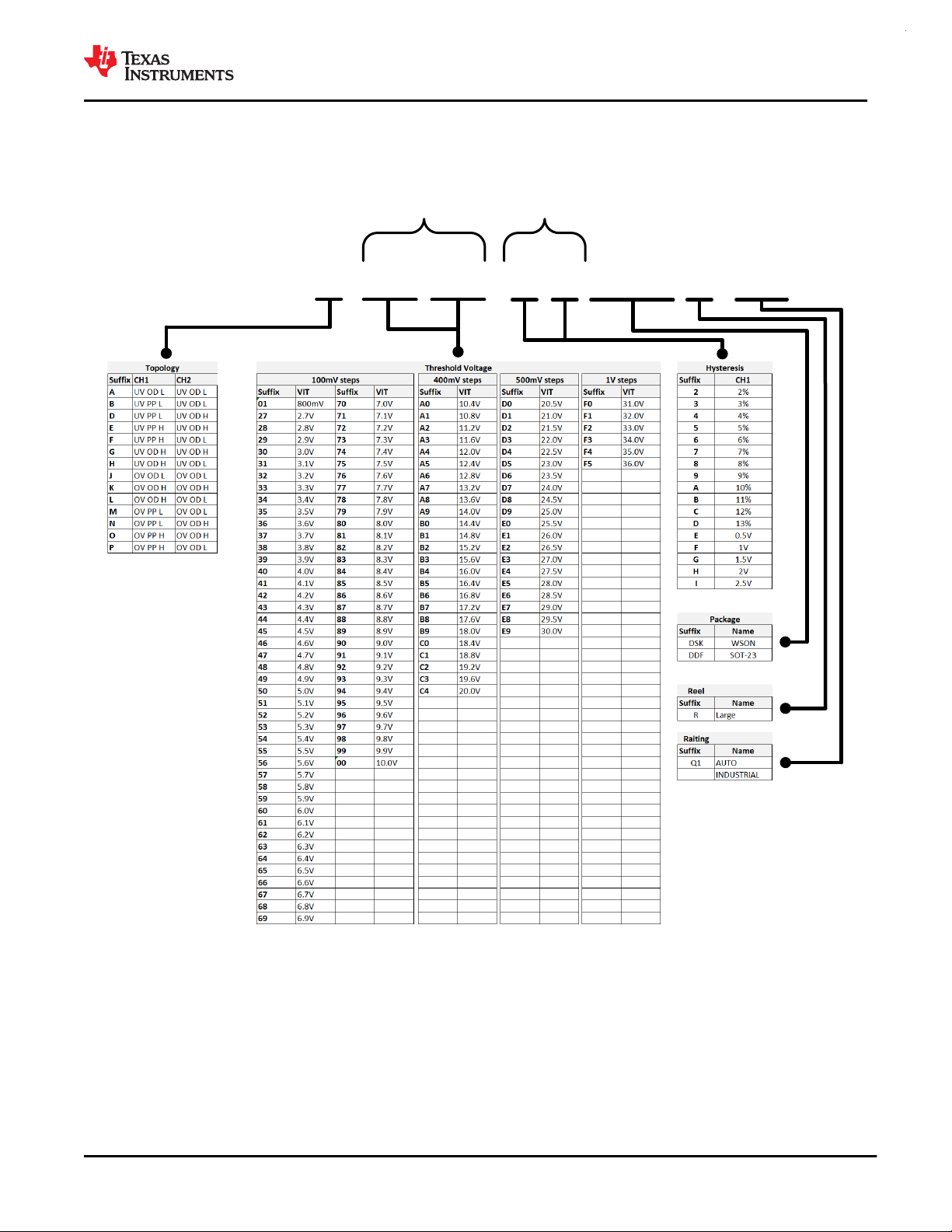
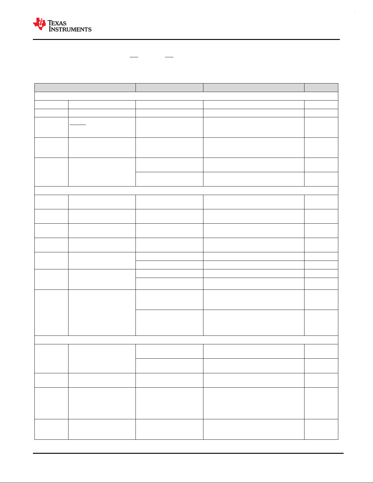
TPS38 X
XX XX
X
X
XXX R -Q1
CH 1
Voltage Threshold
CH 2 CH 1
CH 2
Hysteresis
www.ti.com
ADVANCE INFORMATION
5 Device Comparison
Contact TI sales representatives or consult TI's E2E forum for details and availability; minimum order quantities
may apply.
SNVSBI8A – AUGUST 2020 – REVISED JANUARY 2021
TPS38X-Q1
Figure 5-1. Device Nomenclature
1. Sense logic: OV = overvoltage; UV = undervoltage
2. Reset topology: PP = Push-Pull; OD = Open-Drain
3. Reset logic: L = Active-Low; H = Active-High
4. A to I hysteresis options are only available for 2.9 V to 9 V threshold options
Copyright © 2021 Texas Instruments Incorporated
Product Folder Links: TPS38X-Q1
Submit Document Feedback
3

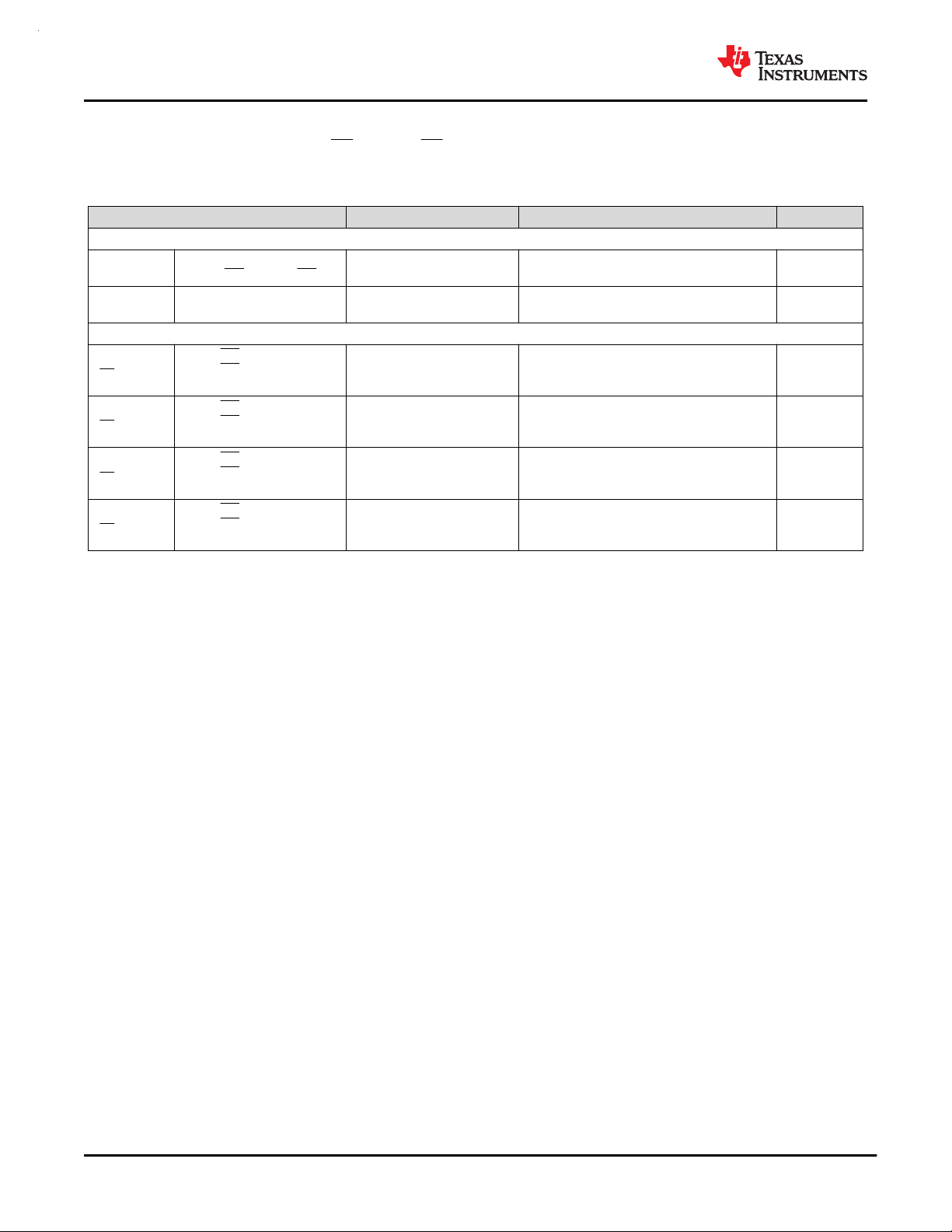
1
2
3
4
5
10
9
8
7
6
VDD
SENSE1
SENSE2
GND
CTR2/MR
RESET1_UVOD
RESET2_UVOD CTR1/MR
CTS1
CTS2
NC
(No Internal Connection)
1
2
3
4
5
10
9
8
7
6
VDD
SENSE1
SENSE2
GND
CTR2/MR
RESET1_UVPP
RESET2_UVOD CTR1/MR
CTS1
CTS2
NC
(No Internal Connection)
1
2
3
4
5
10
9
8
7
6
VDD
SENSE1
SENSE2
GND
CTR2/MR
RESET1_UVPP
CTS1
CTS2
NC
(No Internal Connection)
1
2
3
4
5
10
9
8
7
6
VDD
SENSE1
SENSE2
GND
CTR2/MR
RESET1_UVPP
CTS1
CTS2
NC
(No Internal Connection)
1
2
3
4
5
10
9
8
7
6
VDD
SENSE1
SENSE2
GND
CTR2/MR
RESET1_UVPP
CTS1
CTS2
NC
(No Internal Connection)
1
2
3
4
5
10
9
8
7
6
VDD
SENSE1
SENSE2
GND
CTR2/MR
CTS1
CTS2
NC
(No Internal Connection)
1
2
3
4
5
10
9
8
7
6
VDD
SENSE1
SENSE2
GND
CTR2/MR
CTS1
CTS2
NC
(No Internal Connection)
1
2
3
4
5
10
9
8
7
6
VDD
SENSE1
SENSE2
GND
CTR2/MR
RESET1_OVOD
RESET2_OVOD CTR1/MR
CTS1
CTS2
NC
(No Internal Connection)
TPS38X-Q1
ADVANCE INFORMATION
SNVSBI8A – AUGUST 2020 – REVISED JANUARY 2021
6 Pin Configuration and Functions
www.ti.com
Figure 6-1. DSK Package 10-Pin WSON TPS38A
(Top View)
Figure 6-3. DSK Package 10-Pin WSON TPS38D
(Top View)
Figure 6-5. DSK Package 10-Pin WSON TPS38F
(Top View)
Figure 6-2. DSK Package 10-Pin WSON
TPS38B(Top View)
Figure 6-4. DSK Package 10-Pin WSON TPS38E
(Top View)
Figure 6-6. DSK Package 10-Pin WSON TPS38G
(Top View)
Figure 6-7. DSK Package 10-Pin WSON TPS38H
(Top View)
4 Submit Document Feedback
Figure 6-8. DSK Package 10-Pin WSON TPS38J
(Top View)
Copyright © 2021 Texas Instruments Incorporated
Product Folder Links: TPS38X-Q1

1
2
3
4
5
10
9
8
7
6
VDD
SENSE1
SENSE2
GND
CTR2/MR
CTS1
CTS2
NC
(No Internal Connection)
1
2
3
4
5
10
9
8
7
6
VDD
SENSE1
SENSE2
GND
CTR2/MR
CTS1
CTS2
NC
(No Internal Connection)
1
2
3
4
5
10
9
8
7
6
VDD
SENSE1
SENSE2
GND
CTR2/MR
RESET1_OVPP
CTS1
CTS2
NC
(No Internal Connection)
1
2
3
4
5
10
9
8
7
6
VDD
SENSE1
SENSE2
GND
CTR2/MR
RESET1_OVPP
CTS1
CTS2
NC
(No Internal Connection)
1
2
3
4
5
10
9
8
7
6
VDD
SENSE1
SENSE2
GND
CTR2/MR
RESET1_OVPP
CTS1
CTS2
NC
(No Internal Connection)
1
2
3
4
5
10
9
8
7
6
VDD
SENSE1
SENSE2
GND
CTR2/MR
RESET1_OVPP
RESET2_OVOD CTR1/MR
CTS1
CTS2
NC
(No Internal Connection)
www.ti.com
ADVANCE INFORMATION
SNVSBI8A – AUGUST 2020 – REVISED JANUARY 2021
TPS38X-Q1
Figure 6-9. DSK Package 10-Pin WSON TPS38K
(Top View)
Figure 6-11. DSK Package 10-Pin WSON TPS38M
(Top View)
Figure 6-13. DSK Package 10-Pin WSON TPS38O
(Top View)
Figure 6-10. DSK Package 10-Pin WSON TPS38L
(Top View)
Figure 6-12. DSK Package 10-Pin WSON TPS38N
(Top View)
Figure 6-14. DSK Package 10-Pin WSON TPS38P
(Top View)
PIN
NAME NO.
VDD 1 I Input Supply Voltage.
SENSE1 2 I Input for the monitored supply voltage rail channel 1
SENSE2 3 I Input for the monitored supply voltage rail channel 2
RESET1
RESET1,
RESET2
RESET2,
CTR1/ MR 6
Copyright © 2021 Texas Instruments Incorporated
4 O Output Reset Signal For Channel 1: See Figure 5-1
5 O Output Reset Signal For Channel 2: See Figure 5-1
I/O DESCRIPTION
_ Capacitor Time Delay Reset 1. The CTR1 pin offers a user-programmable reset release delay for
Table 6-1. Pin Functions Generic
Reset1. Connect an external capacitor on this pin to adjust time delay. When not in use leave pin
floating for the fastest time delay.
Manual Reset (CTR1/ MR):If this pin is driven low the RESET1 output will reset, leave pin floating or
connected to a cap to release reset. This pin should not be driven high.
Submit Document Feedback
Product Folder Links: TPS38X-Q1
5
ADVANCE INFORMATION
TPS38X-Q1
SNVSBI8A – AUGUST 2020 – REVISED JANUARY 2021
Table 6-1. Pin Functions Generic (continued)
PIN
NAME NO.
CTR2/ MR 9
GND 10 _ Ground
NC PAD -
CTS1 7
CTS2 8
TPS38A
RESET1_UVOD 4 O Reset output signal for Sense 1. Topology: Undervoltage, Open Drain, Active Low topology.
RESET2_UVOD 5 O Reset output signal for Sense 2. Topology: Undervoltage, Open Drain, Active Low topology.
TPS38B
RESET1_UVPP 4 O Reset output signal for Sense 1. Topology: Undervoltage, Push Pull, Active Low topology.
RESET2_UVOD 5 O Reset output signal for Sense 2. Topology: Undervoltage, Open Drain, Active Low topology.
TPS38D
RESET1_UVPP 4 O Reset output signal for Sense 1. Topology: Undervoltage, Push Pull, Active Low topology.
RESET2_UVOD 5 O Reset output signal for Sense 2. Topology: Undervoltage, Open Drain, Active High topology.
TPS38E
RESET1_UVPP 4 O Reset output signal for Sense 1. Topology: Undervoltage, Push Pull, Active High topology.
RESET2_UVOD 5 O Reset output signal for Sense 2. Topology: Undervoltage, Open Drain, Active High topology.
TPS38F
RESET1_UVPP 4 O Reset output signal for Sense 1. Topology: Undervoltage, Push Pull, Active High topology.
RESET2_UVOD 5 O Reset output signal for Sense 2. Topology: Undervoltage, Open Drain, Active Low topology.
TPS38G
RESET1_UVOD 4 O Reset output signal for Sense 1. Topology: Undervoltage, Open Drain, Active High topology.
RESET2_UVOD 5 O Reset output signal for Sense 2. Topology: Undervoltage, Open Drain, Active High topology.
TPS38H
RESET1_UVOD 4 O Reset output signal for Sense 1. Topology: Undervoltage, Open Drain, Active High topology.
RESET2_UVOD 5 O Reset output signal for Sense 2. Topology: Undervoltage, Open Drain, Active Low topology.
TPS38J
RESET1_OVOD 4 O Reset output signal for Sense 1. Topology: Overvoltage, Open Drain, Active Low topology.
RESET2_OVOD 5 O Reset output signal for Sense 2. Topology: Overvoltage, Open Drain, Active Low topology.
TPS38K
RESET1_OVOD 4 O Reset output signal for Sense 1. Topology: Overvoltage, Open Drain, Active High topology.
RESET2_OVOD 5 O Reset output signal for Sense 2. Topology: Overvoltage, Open Drain, Active High topology.
TPS38L
RESET1_OVOD 4 O Reset output signal for Sense 1. Topology: Overvoltage, Open Drain, Active High topology.
RESET2_OVOD 5 O Reset output signal for Sense 2. Topology: Overvoltage, Open Drain, Active Low topology.
TPS38M
RESET1_OVPP 4 O Reset output signal for Sense 1. Topology: Overvoltage, Push Pull, Active Low topology.
RESET2_OVOD 5 O Reset output signal for Sense 2. Topology: Overvoltage, Open Drain, Active Low topology.
I/O DESCRIPTION
_ Capacitor Time Delay Reset 2. The CTR2 pin offers a user-programmable reset release delay for
Reset2. Connect an external capacitor on this pin to adjust time delay. When not in use leave pin
floating for the fastest time delay.
Manual Reset (CTR2/ MR):If this pin is driven low the RESET2 output will reset, leave pin floating or
connected to a cap to release reset. This pin should not be driven high.
Not internally connected, is recommended to leave the central pad floating for wider creepage
between VDD and GND.
_ Capacitor Time Delay Sense 1. The CTS1 pin offers a user-programmable sense delay for Sense1.
Connect an external capacitor on this pin to adjust time delay. When not in use leave pin floating for
the fastest time delay.
_ Capacitor Time Delay Sense 2. The CTS2 pin offers a user-programmable sense delay for Sense2.
Connect an external capacitor on this pin to adjust time delay. When not in use leave pin floating for
the fastest time delay.
www.ti.com
6 Submit Document Feedback
Copyright © 2021 Texas Instruments Incorporated
Product Folder Links: TPS38X-Q1
www.ti.com
ADVANCE INFORMATION
SNVSBI8A – AUGUST 2020 – REVISED JANUARY 2021
Table 6-1. Pin Functions Generic (continued)
PIN
NAME NO.
TPS38N
RESET1_OVPP 4 O Reset output signal for Sense 1. Topology: Overvoltage, Push Pull, Active Low topology.
RESET2_OVOD 5 O Reset output signal for Sense 2. Topology: Overvoltage, Open Drain, Active High topology.
TPS38O
RESET1_OVPP 4 O Reset output signal for Sense 1. Topology: Overvoltage, Push Pull, Active High topology.
RESET2_OVOD 5 O Reset output signal for Sense 2. Topology: Overvoltage, Open Drain, Active High topology.
TPS38P
RESET1_OVPP 4 O Reset output signal for Sense 1. Topology: Overvoltage, Push Pull, Active High topology.
RESET2_OVOD 5 O Reset output signal for Sense 2. Topology: Overvoltage, Open Drain, Active Low topology.
I/O DESCRIPTION
TPS38X-Q1
Copyright © 2021 Texas Instruments Incorporated
Product Folder Links: TPS38X-Q1
Submit Document Feedback
7
ADVANCE INFORMATION
TPS38X-Q1
SNVSBI8A – AUGUST 2020 – REVISED JANUARY 2021
www.ti.com
7 Specifications
7.1 Absolute Maximum Ratings
over operating free-air temperature range, unless otherwise noted
Voltage VDD, V
Voltage V
Current I
Temperature
Temperature
Temperature
(2)
(2)
(2)
SENSE1,VSENSE2
, V
CTS2
, I
RESET2
, V
CTS1
RESET1
Operating junction temperature, T
Operating Ambient temperature, T
Storage, T
stg
(1) Stresses beyond those listed under Absolute Maximum Ratings may cause permanent damage to the device. These are stress ratings
only, which do not imply functional operation of the device at these or any other conditions beyond those indicated under
Recommended Operating Conditions. Exposure to absolute-maximum-rated conditions for extended periods may affect device
reliability.
(2) As a result of the low dissipated power in this device, it is assumed that TJ = TA.
CTR1
, I
RESET1
, V
, V
CTR2
, I
RESET1
RESET2
, V
7.2 ESD Ratings
Human body model (HBM), per AEC Q100-002
V
(1) AEC Q100-002 indicates that HBM stressing shall be in accordance with the ANSI/ESDA/JEDEC JS-001 specification.
Electrostatic discharge
(ESD)
Charged device model (CDM), per
AEC Q100-011
RESET2
J
A
(1)
, V
RESET1
, V
RESET2
MIN MAX UNIT
–0.3 70
–0.3 6
10 mA
–40 150 °C
–40 150 °C
–65 150 °C
VALUE UNIT
(1)
±2000
±750
V
7.3 Recommended Operating Conditions
over operating free-air temperature range (unless otherwise noted)
MIN NOM MAX UNIT
Voltage V
Voltage V
Voltage V
Current I
T
J
DD
SENSE1,VSENSE2
, V
CTS1
CTS2
, I
RESET1
RESET2
, V
, V
CTR1
, I
RESET1
RESET1
, V
CTR2
, V
, I
RESET2
RESET2
, V
RESET1
, V
RESET2
Junction temperature (free air temperature) –40 125 °C
2.7 65 V
0 65 V
0 5.5 V
0 ±5 mA
7.4 Thermal Information
(1)
R
θJA
R
θJC(top)
R
θJB
ψ
JT
ψ
JB
R
θJC(bot)
THERMAL METRIC
Junction-to-ambient thermal resistance 87.4 °C/W
Junction-to-case (top) thermal resistance 76.3 °C/W
Junction-to-board thermal resistance 54.2 °C/W
Junction-to-top characterization parameter 4.8 °C/W
Junction-to-board characterization parameter 54.2 °C/W
Junction-to-case (bottom) thermal resistance 34.8 °C/W
(1) For more information about traditional and new thermal metrics, see the Semiconductor and IC Package Thermal Metrics application
report.
DSK
10-PIN
UNIT
8 Submit Document Feedback
Copyright © 2021 Texas Instruments Incorporated
Product Folder Links: TPS38X-Q1
ADVANCE INFORMATION
www.ti.com
SNVSBI8A – AUGUST 2020 – REVISED JANUARY 2021
7.5 Electrical Characteristics
TPS38X-Q1
At V
(R
PULLUP
DD (MIN)
≤ VDD ≤ V
DD (MAX)
, CTR1 /
) = 10 kΩ, Output reset Pullup Voltage (V
free-air temperature range – 40°C to 125°C, unless otherwise noted. Typical values are at TJ = 25°C and VDD = 16 V and
VIT = 6.5 V (VIT refers to V
PARAMETER TEST CONDITIONS MIN TYP MAX UNIT
VDD
V
DD
(2)
UVLO
V
POR
V
POR
I
DD
SENSE (Input)
I
SENSE
I
SENSE
I
SENSE
I
SENSE
V
ITN
V
ITP
V
HYS
RESET (output)
I
lkg(OD)
(4)
V
OL
V
OH_DO
(4)
V
OH
Supply Voltage 2.7 65 V
Under Voltage Lockout V
Power on Reset Voltage
RESET, Active Low
(Open-Drain, Push-Pull )
Power on Reset Voltage
RESET, Active High
(Push-Pull )
Supply current into VDD pin
Input current
(SENSE1, SENSE2)
Input current
(SENSE1, SENSE2)
Input current
(SENSE1, SENSE2)
Input current
(SENSE1, SENSE2)
Input Threshold Negative
(Under-Voltage)
Input Threshold Positive
(Over-Voltage)
Hysteresis Accuracy
Open-Drain leakage
(RESET1, RESET2)
Low level output voltage
High level output voltage
dropout
(VDD - V
(Push-Pull only)
High level output voltage
(Push-Pull only)
OH
= V
ITN
OH_DO
or V
MR = CTR2 / MR = CTS1 = CTS2 = Open, Output reset Pullup Resistor
) = 5.5 V, output reset load (C
PULLUP
).
ITP
Falling below V
(5)
(5)
DD
V
OL(max)
I
OUT (Sink)
V
OH(min)
I
OUT (Source)
= 300 mV
= 15 µA
= 0.8 x V
= 15 µA
DD (MIN)
DD
VIT = 800 mV
V
DD (MIN)
≤ VDD ≤ V
DD (MAX)
VIT = 2.7 V to 36 V
V
DD (MIN)
≤ VDD ≤ V
DD (MAX)
VIT = 800 mV 100 nA
VIT < 10 V
10 V < VIT < 26 V
VIT > 26 V
VIT = 2.7 V to 36 V -1.5 1.5 %
VIT = 800 mV
(3)
0.792 0.800 0.808 V
VIT = 2.7 V to 36 V -1.5 1.5 %
VIT = 800 mV
(3)
0.792 0.800 0.808 V
VIT = 0.8 V and 2.7 V to 36 V
V
Range = 2% to 13%
HYS
-1.5 1.5 %
(1% step)
(1)
VIT = 2.7 V to 8 V
V
= 0.5 V, 1 V, 1.5 V, 2 V,
HYS
2.5 V
VIT-V
V
V
V
V
RESET
< V
ITN
RESET
< V
ITN
≥ 2.4 V
HYS
= 5.5 V
SENSE
= 65 V
SENSE
< V
< V
-1.5 1.5 %
ITP
ITP
2.7 V ≤ VDD ≤ 65 V
I
= 5 mA
RESET
)
2.7 V ≤ VDD ≤ 65 V
I
= 500 uA
RESET
2.7 V ≤ VDD ≤ 65 V
I
= 5 mA
RESET
0.8V
DD
) = 10 pF and over the operating
LOAD
1 2.6 µA
1 2 µA
2.7 V
1.4 V
1.4 V
0.8 uA
1.2 uA
2 uA
300 nA
300 nA
300 mV
43 mV
V
Copyright © 2021 Texas Instruments Incorporated
Product Folder Links: TPS38X-Q1
Submit Document Feedback
9
ADVANCE INFORMATION
TPS38X-Q1
SNVSBI8A – AUGUST 2020 – REVISED JANUARY 2021
www.ti.com
7.5 Electrical Characteristics (continued)
At V
(R
PULLUP
DD (MIN)
≤ VDD ≤ V
DD (MAX)
, CTR1 /
) = 10 kΩ, Output reset Pullup Voltage (V
free-air temperature range – 40°C to 125°C, unless otherwise noted. Typical values are at TJ = 25°C and VDD = 16 V and
VIT = 6.5 V (VIT refers to V
PARAMETER TEST CONDITIONS MIN TYP MAX UNIT
Capacitor Timing (CTS, CTR)
R
CTR
R
CTS
Manual Reset (MR)
V
MR_IH
V
MR_IH
V
MR_IL
V
MR_IL
(1) Hysteresis is with respect to V
(2) When VDD voltage falls below UVLO, reset is asserted for Output 1 and Output 2. VDD slew rate ≤ 100mV/µs
(3) For adjustable voltage guidelines and resistor selection refer to Adjustable Voltage Thresholds in Application and Implementation
section
(4) For VOH and VOL relation to output variants refer to Timing Figures after the Timing Requirement Table
(5) V
POR
Internal resistance
(CTR1 / MR , CTR2 / MR )
Internal resistance
(C
TS1, CTS2
CTR1 / MR and
CTR2 / MR pin
logic high input
CTR1 / MR and
CTR2 / MR pin
logic high input
CTR1 / MR and
CTR2 / MR pin
logic low input
CTR1 / MR and
CTR2 / MR pin
logic low input
is the minimum VDD voltage for a controlled output state. Below VPOR, the output cannot be determined. VDD dv/dt ≤ 100mV/µs
)
ITN
or V
MR = CTR2 / MR = CTS1 = CTS2 = Open, Output reset Pullup Resistor
ITP
).
ITP
and V
) = 5.5 V, output reset load (C
PULLUP
877 1000 1147 Kohms
88 100 122 Kohms
VDD = 2.7 V 2000 mV
VDD = 65 V 2500 mV
VDD = 2.7 V 1300 mV
VDD = 65 V 1300 mV
voltage threshold. V
ITN
has negative hysteresis and V
ITP
) = 10 pF and over the operating
LOAD
has positive hysteresis.
ITN
10 Submit Document Feedback
Copyright © 2021 Texas Instruments Incorporated
Product Folder Links: TPS38X-Q1
www.ti.com
ADVANCE INFORMATION
SNVSBI8A – AUGUST 2020 – REVISED JANUARY 2021
TPS38X-Q1
7.6 Timing Requirements
At V
DD_(MIN)
10 kΩ, Output reset Pullup Voltage (V
≤ VDD ≤ VDD_
, CTR1/MR = CTR2/MR = CTS1 = CTS2 = Open
(MAX)
) = 5.5V, output reset load (C
PULLUP
us, over the operating free-air temperature range – 40°C to 125°C, unless otherwise noted. Typical values are at TJ = 25°C
and VDD=16 V and VIT = 6.5 V (VIT refers to either V
PARAMETER TEST CONDITIONS MIN TYP MAX UNIT
Common timing parameters
VIT = 2.7 V to 36 V
C
= C
= C
= C
= C
TR1
TR2
TR2
TS2
TS2
= C
= C
= Open
= Open
= Open
= Open
TR2
TR1
t
CTR
Reset release time delay
(CTR1/MR, CTR2/MR)
20% Overdrive from Hysteresis
(3)
VIT = 800 mV
C
TR1
20% Overdrive from Hysteresis
VIT = 2.7 V to 36 V
C
TS1
t
CTS
Sense detect time delay
(CTS1, CTS2)
(4)
20% Overdrive from V
VIT = 800 mV
C
TS1
20% Overdrive from V
C
t
SD
(1) C
Startup Delay
= Reset delay channel 1, C
TR1
C
= Sense delay channel 1, C
TS1
(2)
TR1/MR
= Reset delay channel 2,
TR2
= Sense delay channel 2
TS2
(2) During the power-on sequence,VDD mustbe at or above VDD (MIN) for at least t
V
.
SENSE
t
time includes the propagation delay (C
SD
(3) CTR Reset detect time delay:
OVER-voltage active-LOW output is measure from V
UNDER-voltage active-LOW output is measure from V
OVER-voltage active-HIGH output is measure from V
UNDER-voltage active-HIGH output is measure from V
(4) CTS Sense detect time delay:
Active-low output is measure from VIT to VOL (or V
Active-high output is measured from VIT to VOH
VIT refers to either V
ITN
or V
ITP
or V
ITN
).
ITP
IT
IT
= Open
= Open). Capaicitor in C
TR2
to V
ITP - HYS
ITP - HYS
Pullup
ITN + HYS
ITN + HYS
)
to V
to V
to V
OH
OH
OL
OL
(1)
, Output reset Pullup Resistor (R
) = 10 pF, VDD and SENSE slew rate = 1V/
LOAD
100 us
40 us
34 90 us
8 11 us
before the output is in the correct state based on
SD
or C
TR1
will add time to t
TR2
SD.
PULLUP
2 ms
) =
Copyright © 2021 Texas Instruments Incorporated
Product Folder Links: TPS38X-Q1
Submit Document Feedback
11
 Loading...